an-1162 using the lmx3162 for 2.4-ghz ism band · an-1162 using the lmx3162 for 2.4-ghz ism band...
TRANSCRIPT

LMX3162
AN-1162 Using the LMX3162 for 2.4-GHz ISM Band
Literature Number: SNOA089
Using the LMX3162 for2.4-GHz ISM Band
TABLE OF CONTENTS
1.0 ABSTRACT
2.0 INTRODUCTION
3.0 STANDARDS
4.0 TRANSCEIVER DESIGN
4.1 SYNTHESIZER
4.1.1 Lock Time
4.2 TRANSMITTER
4.3 RECEIVER
4.3.1 Demodulation Parallel Tank
4.3.2 Performance
5.0 CONCLUSION
LIST OF FIGURES
FIGURE 1. Transceiver Blocks
FIGURE 2. Timing for Open Loop Operation
FIGURE 3. Ultra Low Drift PLL
FIGURE 4. PLL Lock Time
FIGURE 5. Open Loop Frequency Drift at 85˚C
FIGURE 6. Bluetooth Modulated Signals
FIGURE 7. (a) Tx Block. (b) Rx Block
FIGURE 8. Harmonics of Transmitter Output
FIGURE 9. Phase Noise of Local Oscillator
FIGURE 10. LNA/PA in Low-Power Mode
FIGURE 11. Receiver Chain Analysis
FIGURE 12. Quadrature Demodulation
FIGURE 13. Parallel Quadrature Tank
FIGURE 14. Eye Diagram, BER=1e−3, −83 dBm
FIGURE 15. Eye Diagram, BER=0, −40 dBm
FIGURE 16. Eye Diagram for Bluetooth CCI Test
FIGURE 17. Eye Diagram for Bluetooth ACI 1-MHz Test
FIGURE 18. Eye Diagram for Bluetooth ACI 2-MHz Test.(−81 dBm)
FIGURE 19. Eye Diagram for Bluetooth ACI 3-MHz Test.(−72 dBm)
FIGURE 20. Bluetooth Intermodulation Test
FIGURE 21. Optional LNA/PA for Bluetooth orHomeRF/Upbanded DECT
FIGURE 22. Optimized Schematics of LMX3162 Evalua-tion Board (include Tx buffer)
LIST OF TABLES
TABLE 1. Parameter Comparison for 2.4-GHz Applications
TABLE 2. Interference Test for Bluetooth
TABLE 3. Bill of Materials for LMX3162
1.0 ABSTRACT
A monolithic radio transceiver will be demonstrated for theemerging wireless data and voice applications in the unli-censed 2.4-GHz ISM band including Bluetooth, HomeRFand Upbanded DECT standards. The architecture and thefunctionality of the LMX3162 will be described thoroughly.The circuit blocks and the topology will be discussed toimplement the complete radio with the measuring perfor-mance. These results illustrate the single-chip LMX3162 is apossible solution to support the various standards in ISMband.
2.0 INTRODUCTION
Higher and higher levels of integration in RF circuits havebecome the trend over the past decade. For example, thecomplete receiver on a chip has been available in the indus-tries for many years ago. The LMX3162 integrated circuit(IC) takes radio integration one step further by including re-ceiver, transmitter, and the phase locked loop (PLL) on thesame piece of silicon. In accordance with a 1.3-GHz PLL, afrequency doubler is employed and both the receiver and thetransmitter can share the same PLL. This reduces the com-plexity of the system as well as avoiding the problem of injec-tion locking or LO pulling in the VCO. Figure 1 shows a typi-cal implementation of a 2.4-GHz radio front-end transceiver.In addition to the PLL and frequency doubler, a 2.5-GHzlow-noise mixer, intermediate-frequency (IF) amplifier, limit-ing amplifier, frequency discriminator, and received-signal-strength indicator (RSSI) for the receiver, as well as abuffer amplifier for the transmitter are integrated inLMX3162[1][2]. Only a few of channel selection filters, VCOand loop filters are required external components1. The dis-crete low noise amplifier (LNA) and power amplifier (PA) areoptional depending on system requirements for the variousstandards and applications.
New standards have been developed for the explodingHome PC, handheld service access and information appli-ance market. For this reason, the unlicensed 2.4-GHz Indus-trial, Scientific and Medical (ISM) band has been received agreat amount of interest in the wireless communications in-dustry worldwide. The common frequency range (2.4 GHz to2.483 GHz) in Europe, Japan and the USA has also madethis band attractive to many product manufacturers. Severalcompanies have their own solutions available in the markettoday. The open standards will guarantee inter-operabilitybetween products of different brands as well as gain cus-tomer acceptance and market penetration. Recently, therehas been much activity developing products based on Blue-tooth and HomeRF protocols.[3][4]1The VCO regulator and biasing capacitors are not includedhere.
MICROWIRE™ is a trademark of National Semiconductor Corporation.
National SemiconductorAN-1162Wireless CommunicationJanuary 2000
Using
theLM
X3162
for2.4-G
Hz
ISM
Band
AN
-1162
© 2000 National Semiconductor Corporation AN101312 www.national.com

3.0 STANDARDS
Bluetooth2 is a standard for radio-based wireless ports with10–100 m range as a wireless pico-LAN. In comparison, theShared Wireless Access Protocol-Cordless Access orSWAP-CA is focused on the home networking with 300 mrange. Another option is moving the Digital Enhanced Cord-less Telephone (DECT) to the 2.4-GHz band since bothBluetooth and HomeRF are loosely based on the DECT. Allthese standards are specifically designed with frequencyhopping algorithms to work well in the presence of micro-wave ovens and also include page mode to maximize bat-tery life. An overview of the different standards is shown inTable 1.2Bluetooth frequency range is for US only.
The Bluetooth and HomeRF performance requirements areless stringent as the DECT standards. For examples, thesensitivity and the in-band blocking levels are much relaxed.In particular, HomeRF does not need an adjacent channelspecification and only requires co-channel interference atthe third channel −10 dB below the signal. Moreover, the in-
termodulation product (IIP3) requires only −39.5 dBm. Giventhese relaxed standards, the LNA is an optional device forBluetooth and HomeRF. Without the LNA, LMX3162 canachieve the sensitivity of −83 dBm. This further reduces thenumber of external components and power consumption.The power amplifier is also optional because two classes oftransmitting power defined in both Bluetooth and HomeRF.
Deploying Bluetooth and HomeRF in accordance with DECTstandard, the difference between the masks of transmitspectrum, as FCC part 15[5], should be noticed. In DECT, itis not 20 dB down at 1-MHz offset from the desired channel,where the data rate is 1.152 Mbits/s in GFSK and the BTproduct equals to 0.5.
There are two ways to resolve this issue. For minimal im-pact, simply lowering the bit rate to 1 Mbits/s while keepingthe same BT product will decrease the bandwidth of thetransmit spectrum to meet the requirements. For full DECTdata rate, the alternative method is to reduce the BT productto 0.35 so that the spectrum can be met. However, the in-tersymbol interference (ISI) will be degraded by several dB.
TABLE 1. Parameter Comparison for 2.4-GHz Applications
Parameters Bluetooth HomeRF Upbanded DECT
FREQUENCY
Band 2.402 GHz–2.480 GHz 2.404 GHz–2.478 GHz 2.40 GHz–2.483 GHz
Channel Spacing 1.000 MHz 1.000 MHz ≥1.000 MHz
Accuracy ±75 kHz ±120 kHz ±50 kHz
Lock Time (est) 220 µs 134 µs 30 µs(416.67 µs w/1 Blind Slot)
Drift ±40 kHz/5 Slots NA ±40 kHz/ms
MODULATION
Type GFSK 2-FSK (4-FSK) GFSK
Deviation Min ±140 kHz ±85 kHz ±135 kHz ±200 kHz nom
Max ±175 kHz ±177.5 kHz ±190 kHz (±250 kHz nom)
Burst Bit Rate 1 Mbits/s 0.8 Mbit/s 1.6 Mbit/s 1.152 Mbits/s (1.0 Mbits/s)
AN101312-1
FIGURE 1. Transceiver Blocks
AN
-116
2
www.national.com 2
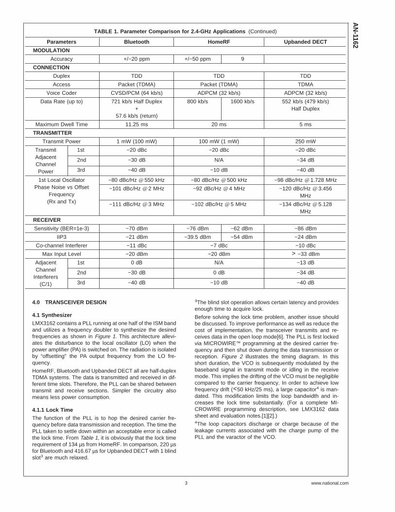
TABLE 1. Parameter Comparison for 2.4-GHz Applications (Continued)
Parameters Bluetooth HomeRF Upbanded DECT
MODULATION
Accuracy +/−20 ppm +/−50 ppm 9
CONNECTION
Duplex TDD TDD TDD
Access Packet (TDMA) Packet (TDMA) TDMA
Voice Coder CVSD/PCM (64 kb/s) ADPCM (32 kb/s) ADPCM (32 kb/s)
Data Rate (up to) 721 kb/s Half Duplex+
57.6 kb/s (return)
800 kb/s 1600 kb/s 552 kb/s (479 kb/s)Half Duplex
Maximum Dwell Time 11.25 ms 20 ms 5 ms
TRANSMITTER
Transmit Power 1 mW (100 mW) 100 mW (1 mW) 250 mW
TransmitAdjacentChannelPower
1st −20 dBc −20 dBc −20 dBc
2nd −30 dB N/A −34 dB
3rd −40 dB −10 dB −40 dB
1st Local OscillatorPhase Noise vs Offset
Frequency(Rx and Tx)
−80 dBc/Hz @ 550 kHz −80 dBc/Hz @ 500 kHz −98 dBc/Hz @ 1.728 MHz
−101 dBc/Hz @ 2 MHz −92 dBc/Hz @ 4 MHz −120 dBc/Hz @ 3.456MHz
−111 dBc/Hz @ 3 MHz −102 dBc/Hz @ 5 MHz −134 dBc/Hz @ 5.128MHz
RECEIVER
Sensitivity (BER=1e-3) −70 dBm −76 dBm −62 dBm −86 dBm
IIP3 −21 dBm −39.5 dBm −54 dBm −24 dBm
Co-channel Interferer −11 dBc −7 dBc −10 dBc
Max Input Level −20 dBm −20 dBm > −33 dBm
AdjacentChannel
Interferers(C/1)
1st 0 dB N/A −13 dB
2nd −30 dB 0 dB −34 dB
3rd −40 dB −10 dB −40 dB
4.0 TRANSCEIVER DESIGN
4.1 Synthesizer
LMX3162 contains a PLL running at one half of the ISM bandand utilizes a frequency doubler to synthesize the desiredfrequencies as shown in Figure 1. This architecture allevi-ates the disturbance to the local oscillator (LO) when thepower amplifier (PA) is switched on. The radiation is isolatedby “offsetting″ the PA output frequency from the LO fre-quency.
HomeRF, Bluetooth and Upbanded DECT all are half-duplexTDMA systems. The data is transmitted and received in dif-ferent time slots. Therefore, the PLL can be shared betweentransmit and receive sections. Simpler the circuitry alsomeans less power consumption.
4.1.1 Lock Time
The function of the PLL is to hop the desired carrier fre-quency before data transmission and reception. The time thePLL taken to settle down within an acceptable error is calledthe lock time. From Table 1, it is obviously that the lock timerequirement of 134 µs from HomeRF. In comparison, 220 µsfor Bluetooth and 416.67 µs for Upbanded DECT with 1 blindslot3 are much relaxed.
3The blind slot operation allows certain latency and providesenough time to acquire lock.
Before solving the lock time problem, another issue shouldbe discussed. To improve performance as well as reduce thecost of implementation, the transceiver transmits and re-ceives data in the open loop mode[6]. The PLL is first lockedvia MICROWIRE™ programming at the desired carrier fre-quency and then shut down during the data transmission orreception. Figure 2 illustrates the timing diagram. In thisshort duration, the VCO is subsequently modulated by thebaseband signal in transmit mode or idling in the receivemode. This implies the drifting of the VCO must be negligiblecompared to the carrier frequency. In order to achieve lowfrequency drift (<50 kHz/25 ms), a large capacitor4 is man-dated. This modification limits the loop bandwidth and in-creases the lock time substantially. (For a complete MI-CROWIRE programming description, see LMX3162 datasheet and evaluation notes.[1][2].)4The loop capacitors discharge or charge because of theleakage currents associated with the charge pump of thePLL and the varactor of the VCO.
AN
-1162
www.national.com3

To resolve this issue (in particular for HomerRF), a unity gainop-amp, a CMOS sampling switch and a low-leakage ca-pacitor are employed between the loop filter and the controlline of the VCO, as illustrated in Figure 3. This configurationhandles the lock time and current leakage requirements byusing different values of capacitors. With this implementa-tion, a small capacitor in the loop filter is used to provide loopbandwidth and phase margin to achieve the required locktime while a large capacitor (CS) at the control line of theVCO reduces the frequency drift. The unity gain op-amp du-plicates the information (voltage) stored to the low-leakagecapacitor (large capacitor) while the PLL is in lock. In theopen loop mode, the CMOS sampling switch is used to sus-pend the operation of the op-amp with sufficient isolation ofthese capacitors. Once the PLL is closed, the switch re-sumes the sampling operation. The choice of this capacitordepends on dielectric radiation properties of the material.Polypropylene or even better capacitor is advisable.
The VCO gain (KVCO) is 110 MHz/V referred to 2.4 GHz. Thephase detector comparison frequency is 250 kHz5. A secondorder loop filter is designed with the loop bandwidth 40 kHzand the phase margin 50˚. Figure 3 shows the componentvalues of the filter. The lock time is measured from the fallingedge of signal that shuts down the PLL (PLL_PD) to 1225MHz (2450 MHz at Tx Output) within 5 kHz (10 kHz at Txoutput). The lock time is 111 µs as shown in Figure 4. This isless than HomeRF required.5Given 1-MHz channel spacing and the IF is at 110.5 MHz,the largest comparison frequency is 0.25 MHz because offrequency doubler.
The frequency drift due to the current leakage is measuredstarting from the rising edge of PLL_PD. Figure 5 demon-strates the frequency drift of the VCO at 85˚C. The very lowdrift of 778 Hz/ms is much less than required for HomeRF.There are two frequency jumps. The first is due to the phase
AN101312-2
FIGURE 2. Timing for Open Loop Operation
AN101312-3
FIGURE 3. Ultra Low Drift PLL
AN
-116
2
www.national.com 4

noise of the PLL and appears as a jump due to the finite re-sponse time of the domain modulation analyzer. The secondjump is due to the common mode operating range of theop-amp. Since the large VCO gain, the frequency jumps tensof kilohertz even though only a few hundred µVs fluctuates.Placing a 10-MΩ resistor in parallel with loop filter will sinkaway the bias current of the op-amp and prevent saturation.The occurrence of the second jump depends on the selec-tion of the op-amp and the CMOS switch. In the current de-sign, the second jump occurs only after the loop is open fora long time. (>100 ms). In case of HomeRF, the loop will notbe idle or open for such long period.
For Bluetooth, the maximum continuous transmit time is 5slots, or 3.125 ms. The total loop filter capacitance of about7 nF is needed for 180 µs lock time, which including 40 µsbudget for margins and programming time. Then, the drift in3.125 ms is about 34 kHz by
6The typical value of the leakage current is 700 pA at 85˚C.
which meets the Bluetooth requirement of 40 kHz. This cal-culation tells that LMX3162 meets the requirement evenwithout the additional op-amp, switch and the large capaci-tor.
Table 1 shows that the maximum dwell time is 11.25 ms forBluetooth and 20 ms for HomeRF. However, the transceiveris operating in scan mode. (receiving only) Frequency driftcan be avoided without additional circuitry by closing the PLLand receiving data. This may result in degradation of bit errorrate (BER) by one or two decibel(s), which is acceptablesince LMX3162 gives enough design margins on sensitivity.
4.2 Transmitter
In LMX3162, direct VCO modulation scheme is employed asshown in Figure 7(a). It is simple and low cost solution incomparison to other options, such as direct RF I/Q modula-tion or close loop I/O modulation. In this section, LMX3162will be demonstrated to transmit the data with the open loopmodulation for the 2.4-GHz ISM band.
To transmit a signal, a shaped baseband signal is applied tothe tuning pin7 of the VCO to assure bandwidth efficient. Theamplitude of the signal from the baseband processor needsto be adjusted to obtain the frequency deviation. Given theVCO gain, a resistive divider can be calculated for the cor-rect amplitude to modulate the VCO. The peak frequencydeviation can be measured by a domain modulation ana-lyzer and a spectrum analyzer.7The loop filter or the modulation port of the VCO.
With the correct amplitude of the signal, the VCO output gen-erates the modulated signal and is connected to the input ofthe frequency doubler inside LMX3162. The 2.4-GHz signalat the transmit output pin (TX_OUT) should be filtered inprior feeding to the power amplifier. Otherwise, a phenom-enon called spectra regrowth may occurred.
For Bluetooth in the low power mode, the required transmitpower is 0 dBm. The TX_OUT pin provides an output powerlevel of −7.5 dBm. An amplifier of 10.5-dB gain should besufficient if 1-dB loss in the Transmit/Receive switch and2-dB loss in the post-amplifier ceramic band pass filter areincluded. A simple solution is the single stage amplifier witha bipolar transistor8 biasing at 10 mA with internal voltageregulator supply of LMX3162. For Bluetooth in the highpower node, the power range is as of 20 dBm. A high effi-ciency power amplifier should also be employed. Good can-didates are ITT2304 for Bluetooth and HomeRF, ITT2302 forUpbanded DECT.8The same configuration as the LNA, Siemens BFP420, willbe mentioned in the receive section.
AN101312-4
FIGURE 4. PLL Lock Time
AN101312-5
FIGURE 5. Open Loop Frequency Drift at 85˚C
AN101312-7
FIGURE 6. Bluetooth Modulated Signals
AN
-1162
www.national.com5

Removing all the harmonics and sub-harmonics of the car-rier by filtering is also necessitated after amplification be-cause the transmit spectrum is regulated by FCC. FCC alsorequires the radiated power at offsets of 500 kHz or more tobe 20 dB below the peak power. Figure 6 shows a PRBS15modulated Bluetooth signal at the transmitter output(BT=0.5, GFSK and 320 kHz peak-to-peak frequency devia-tion) and a mask of transmit spectrum generated by a HPESG4433 signal generator for comparison. (The top traceshown in Figure 6 with larger side-lobe is created from thesignal generator.) This indicates the requirement is met. Thewideband unmodulated transmit spectrum is shown in Figure8. The sub-harmonics is −36 dBm without any post-amplifierfiltering, which meets the Bluetooth specification. Thepost-amplifier ceramic filter shown in Figure 1 used for re-ceive filtering can be shared by the transmit also.
The phase noise of LO has to satisfy certain requirements asmentioned in Table 1 because the PLL is in the open loop op-eration either in transmit or receive mode. The unmodulatedsignal shows the phase noise for the transmit signal in Fig-ure 9.
Moreover, the power supply of the VCO should be regulated.In our experiment, an external low noise voltage regulator,National Semiconductor LP2980, is used to isolate the sup-ply of the VCO from any transient, especially for the power
AN101312-8
(a)
AN101312-9
(b)
FIGURE 7. (a) Tx Block. (b) Rx Block
AN101312-10
FIGURE 8. Harmonics of Transmitter Output
AN
-116
2
www.national.com 6

amplifier. Typically, a 20-dBm power amplifier draws morethan 150 mA. The IR voltage drop from the internal resis-tance of the battery and traces on the PCB may be in excessof the allowance without regulation. Given the VCO gain 10MHz/V, the internal resistance of a Ni-MH battery used inhandsets is about 0.25Ω and the series resistance is about22 mΩ for 12 mil wide 35 micron thick copper traces, the to-tal IR drop will be 40.8 mV. If the error budget allocates ±20kHz, this means only ±2 mV is allowed due to the IR voltagedrop.
4.3 Receiver
LMX3162 adopts the heterodyne receiver architecture asshown in Figure 7(b). The demodulated data can be ob-tained by two frequency conversions with some channel se-lection filtering along the receiver path.
The antenna will perceive many frequencies in the air. TheISM band signals will first be selected and the image, whichis 220 MHz9 below the signals, will be suppressed through aceramic band-selection filter. Based on the sensitivity re-
quirements, the signals can feed to the LNA to enhance theperformance of the receiver. LMX3162 meets the BER re-quirements of Bluetooth and HomeRF without the LNA.9The image frequency is 2 IF (110 MHz).
An example is using a single bipolar transistor amplifier asshown in Figure 10. A gain of 10 dB and a noise figure of 3dB can be achieved while consuming approximate 10 mA.The 2.7-V regulated supply can be run from the LMX3162internally.
Once the images are suppressed, the signals can connect tothe RF input of the 2.5-GHz mixer inside LMX3162. The LOport of the mixer is connected to the frequency doubler inter-nally. Since the IF is 110 MHz, the LO frequency should be110 MHz below the RF carrier frequency. The mixer has15-dB gain with 13-dB noise figure, and the OIP3 of thismixer is 7.5 dBm. The system noise figure from LNA to theRC filter is about 6 dB. The analysis of the receiver chain isshown in Figure 11.
AN101312-11
FIGURE 9. Phase Noise of Local Oscillator
AN101312-12
FIGURE 10. LNA/.PA in Low-Power Mode
AN101312-13
FIGURE 11. Receiver Chain Analysis
AN
-1162
www.national.com7

The mixer has OIP3 of 7.5 dBm. With the OIP3 of 20 dBm10
for the IF amplifier, the system OIP3 would be about 16 dBm.We assume SAW and RC filters are linear and negligible forthe nonlinearity. This indicates the linearity of the latter stage(IF amplifier here) is more critical.
After the signal translated to IF, it is possible to do partiallychannel selection. The IF signals is band-limited by the SAWfilter via the matching network. This SAW filter11 is centeredat 110 MHz, and has a 3-dB bandwidth of 1.5 MHz. The mini-mum insertion loss is about 3 dB. The SAW filter providesthe selectivity and prevents spurious components to distortthe signal in the following stages because of non-linearity.
Then, the IF signal is amplified and further suppressing theunwanted interference by an external RC filter before feed-ing to the limiter. This is because the limiter has a large DCgain and is inherently non-linear. Even small interferencemay possibly cause distortion. At the output of the limiter, theIF signal is strong enough for the discriminator to translate tothe baseband. An internal 1-pF capacitor directs the IF signalto input ports of the discriminator and the external tank cir-cuitry provides the correct phase shift between the two in-puts to generate the baseband signal at optimum level. Thepost-detection filtering further limits the noise bandwidth andthe configuration of quadrature demodulation as shown inFigure 12. An automatic the quadrature tank and the applica-tion of S_field on sampling the initial frequency offset be-tween transmitter and receiver are operated with the base-band controller. The description of the automatic tuning tankand the Sample-And-Hold for data slicing comparison canbe found in the evaluation notes.12
10The data sheet did not provide the OIP3 information.20 dBm is a typical number for IF amplifier and is used for il-lustration purpose here.11SAFU110.0MSA45T=>110.0 MHz center
SAFU110.6MSA40T=>110.592 MHz center12Reader can find the description on p. 10 of evaluationnotes.
4.3.1 Demodulation Parallel Tank
The quadrature tank circuit is shown in Figure 13. The resis-tor RT is not physically presented in the circuit. Instead, RT
models the finite value of the quality factor of the tank. Theprinciple of operation is that the internal coupling capacitor(Cl) and the resonant circuit provides instantaneous phaseshifts that correspond to changes in modulation. The multipli-cation of these quadrature signals in the discriminator(mixer) then generates the output demodulated signal.
The transfer function of the quadrature tank can be de-rived[7],
and its resultant phase characteristic of H(jω) is,
In the LMX3162 evaluation board, Cl is an internal 1-pF ca-pacitor. For tuning the quadrature tank at 110 MHz, CT is acombination of a constant (18 pF) and a variable capacitor(2–6 pF).
AN101312-14
FIGURE 12. Quadrature Demodulation
AN
-116
2
www.national.com 8

The choice of inductor entails a compromise among the tun-ing range, the quality factor (Q) and the bandwidth. Largerthe inductor implies higher the Q. The Q of the quadraturetank as well as the filters along the receiver path determinethe bandwidth. Therefore, higher the Q or larger the inductormeans narrower the bandwidth. For instance, extensive fil-terings and moderate Q can lower the noise bandwidth.Then, the sensitivity and the inter-symbol interference bothimprove because the signal-to-noise ratio (SNR) increases.However, if the bandwidth is further reducing and it eventu-ally chops out the signal bandwidth, the SNR, sensitivity andISI obviously degraded. For this reason, 68 nH is used forLT.
4.3.2 Performance
Without the LNA, the transceiver achieves the sensitivity of−83 dBm at the BER of 1e-3, with the received signal offset±115 kHz by Bluetooth standards. This easily meets theBluetooth minimum sensitivity requirement of −70 dBm. Withthe LNA and optimal SAW filter, sensitivity of −93 dBm canbe obtained. The eye diagram of the received signal for BERof 1e-3 at an input power of −83 dBm and BER of 0 at −40dBm are shown Figures 14, 15 respectively.
TABLE 2. Interference Test for Bluetooth
Test Name Conditions Result
BER PLL Locked, No LNA,BER=1E 3 dBm
−83 dBm
CCI C = −60 dBm, C/I = 11 dB Passed
ACI 1 MHz C = −60 dBm, C/I = 4 dB Passed
ACI 2 MHz C = −60 dBm, C/I = 30 dB Passed
ACI 3 MHz C = −67 dBm, C/I = 40 dB Passed
Image C = −67 dBm, C/I = 9 dB Passed
IMD C = −64 dBm,I1, I2 = −39 dBm
Passed
A transceiver must operate with unwanted signals are eitheron the same or adjacent channels. Strong out of band sig-nals can even desensitize the radio completely. Table 2 liststhe specifications to test the receiver in various conditions.
AN101312-17
FIGURE 13. Parallel Quadrature Tank
AN101312-18
FIGURE 14. Eye Diagram, BER =1e-3, −83 dBm
AN101312-19
FIGURE 15. Eye Diagram, BER =0, −40 dBm
AN
-1162
www.national.com9

The first one is Co-Channel Interference (CCI). The radiomeets a BER of 1e-3 with CCI 11 dB below a desired inputeven at the power level −80 dBm. At the specified desiredsignal level of −60 dBm, the radio even meets the BER withCCI that is only 6 dB difference. For this CCI level, LMX3162suffers no degradation in BER sensitivity. Figure 16 showsthe eye diagram for the Bluetooth CCI test.
The second category of interference test is Adjacent Chan-nel Interference (ACI). A radio must achieve an individualBER test of 1e-3 with undesired Bluetooth signals from otherusers at 1-MHz, 2-MHz and 3-MHz offset. The input level ofthe interference is −4 dB13, −30 dB and −40 dB respectively.LMX3162 meets the ACI tests. Figures 17, 18, 19 show theeye diagram for the ACI test at different frequency offset.
The radio meets the relaxed specification for ACI 1-MHz off-set. In these experiment, the low cost SAW filter has a 3 dBbandwidth of 1.5 MHz and is wider than the Bluetooth signalbandwidth. The center frequency of the SAW filter used inthese measurements is 110.6 MHz because a specific SAW
filter (see footnote 11) for these protocols was not availableat the time the measurement was made. However, the spe-cific SAW filter for bluetooth is available now and a narrowerbandwidth filter will improve the performance of theLMX3162.13The three year relaxed specification for the 1-MHz test isan ACI 4 dB below the desired signal.
The last test shown in Table 2 is measuring the intermodula-tion properties. The test measures the sensitivity of the re-ceiver. (BER=1e-3) with the desired signal at −64 dBm, a−39 dBm static sine wave at 3-MHz offset and another Blue-tooth signal at −39 dBm at 4-MHz offset. The intermodulationproduct creates an interference at 2-MHz offset. This fre-quency subsequently mixes with other input frequencies andgenerates an interference falling on the signal indirectly. Thisalso degrades the sensitivity of the receiver. The result
AN101312-20
FIGURE 16. Eye Diagram for Bluetooth CCI Test
AN101312-21
FIGURE 17. Eye Diagram for Bluetooth ACI 1-MHz Test
AN101312-22
FIGURE 18. Eye Diagram for Bluetooth ACI 2-MHZ Test(−81 dBm)
AN101312-23
FIGURE 19. Eye Diagram for Bluetooth ACI 3-MHz Test(−72 dBm)
AN
-116
2
www.national.com 10

shown in Figure 20 captures the spectrum at the RF inputwith 3 signals when the BER is 1e-3 measured at the dis-criminator output.
5.0 CONCLUSION
LMX3162 is capable to support 2.4-GHz ISM applications.The difference in the implementations depend on the variousstandards. Figure 21 summaries the optional devices forimplementing for Bluetooth or HomeRF/Upbanded DECT.List of Materials and an optimized schematic are shown inTable 3 and Figure 22 respectively. For a complete MI-CROWIRE programming description, see LMX3162 datasheet and evaluation notes.[1][2]
REFERENCE NOTES
[1] LMX3162 Datasheet.
[2] LMX3162 Evaluation Notes.
[3] Specification of the Bluetooth System, Version 0.9, May1999.
[4] HomeRF SWAP Specification.
[5] Document CFR47, Part 15, Sections 15.205, 15.209,15.247, Federal Communications Commission, USA.
[6] D.E. Fague, A. Dao and C. Karmel, “Techniques forOpen Loop Modulation of a Wideband VCO for DECT”,Proceedings of the RF Expo, March 1994.
[7] Wireless Communication, ″Demodulating withLMX2240 150 MHz IF Receiver″, National Semiconduc-tor Application Note AN-1020.
AN101312-24
FIGURE 20. Bluetooth Intermodulation Test
AN101312-25
(a) Bluetooth
AN101312-26
(b) HomeRF/Upbanded DECT
FIGURE 21. Optional LNA/PA for Bluetooth orHomeRF/Upbanded DECT
AN
-1162
www.national.com11

TABLE 3. Bill of Materials for LMX3162
SerialNumber
#Used
Part Type Designator Vendor Tolerance Size
1 1 560 pF C1* +/−5% 603
2 1 15 pF C10 +/−5% 603
3 3 0.01 µF C13 C35 C68 +/−5% 603
4 1 0.015 µF C2* +/−5% 603
5 8 100 pFC22 C41 C48 C5 C8 C11C12 C14
+/−5% 603
6 2 not used C23 C3 +/−5% 603
7 2 10 pF C26 C16 +/−5% 603
8 1 2700 pF C33 +/−5% 603
9 2 2.2 µF C38 C39 +/−5% 603
10 1 1000 pF C4 +/−5% 603
11 1 39 pF C40 +/−5% 603
12 3 27 pF C47 C9 C15 +/−5% 603
13 1 15 pF C50 +/−5% 603
14 1 2 pF–6 pF C51* Murata TZBX4Z060BA110 +/−5% 603
15 1 18 pF C52* +/−5% 603
16 1 0.1 µF C53 +/−5% 603
17 3 100 pF C54 C55 C69 +/−5% 603
18 1 47 pF C6 +/−5% 603
19 1 22 pF C7 +/−5% 603
20 1 10 pF C70 +/−5% 603
21 1 LMX3162 IC1
22 1 Fin J1 CDI 5763SF(SMA)
23 1 RSSI J10 CDI 5762SF(SMA)
24 1 Disc Out J11 CDI 5762SF(SMA)
25 1 Thresh J12 CDI 5762SF(SMA)
26 1 VCC J15 CDI 5762SF(SMA)
27 1 Tx OUT J2 CDI 5762SF(SMA)
28 1 Mod In J3 CDI 5762SF(SMA)
29 1 OSC In J33 CDI 5762SF(SMA)
30 1 DC Comp In J4 CDI 5762SF(SMA)
31 1 RF In J5 CDI 5762SF(SMA)
32 1 Vsw J6 CDI 5762SF(SMA)
33 1 10P_HEADER JP1Common Connectors CCU255G HTSM 3203-40G2
34 1 12P_Header JP2Common Connectors CCU255G HTSM 3203-40G3
35 2 2.5 nH L1 L10 CoilCraft +/−10% 603
36 2 3.9 nH L15 L6 CoilCraft +/−10% 603
37 1 68 nH L16 CoilCraft +/−10% 603
38 1 150 nH L2 CoilCraft +/−10% 603
39 1 220 nH L3 CoilCraft +/−10% 603
40 4 3.9 nH L4 L7 L8 L9 CoilCraft +/−10%
41 1 120 nH L5 CoilCraft +/−10% 603
42 2 BFP420E-6327 Q1, Q3 Siemens
43 1 mmBT3904 Q2 Fairchild
44 2 3.3k R1 R5 +/−10%
45 1 3.9k R10 +/−10%
46 6 not used R11 R13 R15 R16 R31 R6 +/−10%
AN
-116
2
www.national.com 12

TABLE 3. Bill of Materials for LMX3162 (Continued)
SerialNumber
#Used
Part Type Designator Vendor Tolerance Size
47 9 18R14 R19 R23 R24 R25 R26R27 R4 49
+/−10%
48 2 100 R17 R7 +/−10%
49 2 100 R18 R8 +/−10%
50 1 1.2k R2 +/−10%
51 2 0 R21 R40 +/−10%
52 1 51 R22 +/−10%
53 2 6.8k R28 R9 +/−10%
54 1 1k R29 +/−10%
55 1 82k R3 +/−10%
56 1 3.9k R36 +/−10%
57 1 Out 2 TP3
58 1 Out 1 TP4
59 1 Out 0 TP5
60 1 Trigger TP6
61 1DFC22R44P084LHA,Murata
U2
62 1UCVE8X805A orURAE8X630B, ALPS
U3
63 1 LP2980AIM5 U4 National Semiconductor
64 1SAFU110.0MSA45T,Murata
U5
*All capacitors are X7R type. The Capacitor (with asterisk *) C1, C2, C51, C52 are recommended to use lower ESR to avoid leakage.**URAE8X630B is soon replaced by modified version UCVE8X805A, ALPS.
AN
-1162
www.national.com13

AN
1013
12-2
7
FIG
UR
E22
.O
ptim
ized
Sch
emat
ics
ofLM
X31
62E
valu
atio
nB
oard
(incl
ude
Tx
buffe
r)
AN
-116
2
www.national.com 14

Notes
LIFE SUPPORT POLICY
NATIONAL’S PRODUCTS ARE NOT AUTHORIZED FOR USE AS CRITICAL COMPONENTS IN LIFE SUPPORTDEVICES OR SYSTEMS WITHOUT THE EXPRESS WRITTEN APPROVAL OF THE PRESIDENT AND GENERALCOUNSEL OF NATIONAL SEMICONDUCTOR CORPORATION. As used herein:
1. Life support devices or systems are devices orsystems which, (a) are intended for surgical implantinto the body, or (b) support or sustain life, andwhose failure to perform when properly used inaccordance with instructions for use provided in thelabeling, can be reasonably expected to result in asignificant injury to the user.
2. A critical component is any component of a lifesupport device or system whose failure to performcan be reasonably expected to cause the failure ofthe life support device or system, or to affect itssafety or effectiveness.
National SemiconductorCorporationAmericasTel: 1-800-272-9959Fax: 1-800-737-7018Email: [email protected]
National SemiconductorEurope
Fax: +49 (0) 180-530 85 86Email: [email protected]
Deutsch Tel: +49 (0) 69 9508 6208English Tel: +44 (0) 870 24 0 2171Français Tel: +33 (0) 1 41 91 8790
National SemiconductorAsia Pacific CustomerResponse GroupTel: 65-2544466Fax: 65-2504466Email: [email protected]
National SemiconductorJapan Ltd.Tel: 81-3-5639-7560Fax: 81-3-5639-7507
www.national.com
Using
theLM
X3162
for2.4-G
Hz
ISM
Band
AN
-1162
National does not assume any responsibility for use of any circuitry described, no circuit patent licenses are implied and National reserves the right at any time without notice to change said circuitry and specifications.

IMPORTANT NOTICE
Texas Instruments Incorporated and its subsidiaries (TI) reserve the right to make corrections, modifications, enhancements, improvements,and other changes to its products and services at any time and to discontinue any product or service without notice. Customers shouldobtain the latest relevant information before placing orders and should verify that such information is current and complete. All products aresold subject to TI’s terms and conditions of sale supplied at the time of order acknowledgment.
TI warrants performance of its hardware products to the specifications applicable at the time of sale in accordance with TI’s standardwarranty. Testing and other quality control techniques are used to the extent TI deems necessary to support this warranty. Except wheremandated by government requirements, testing of all parameters of each product is not necessarily performed.
TI assumes no liability for applications assistance or customer product design. Customers are responsible for their products andapplications using TI components. To minimize the risks associated with customer products and applications, customers should provideadequate design and operating safeguards.
TI does not warrant or represent that any license, either express or implied, is granted under any TI patent right, copyright, mask work right,or other TI intellectual property right relating to any combination, machine, or process in which TI products or services are used. Informationpublished by TI regarding third-party products or services does not constitute a license from TI to use such products or services or awarranty or endorsement thereof. Use of such information may require a license from a third party under the patents or other intellectualproperty of the third party, or a license from TI under the patents or other intellectual property of TI.
Reproduction of TI information in TI data books or data sheets is permissible only if reproduction is without alteration and is accompaniedby all associated warranties, conditions, limitations, and notices. Reproduction of this information with alteration is an unfair and deceptivebusiness practice. TI is not responsible or liable for such altered documentation. Information of third parties may be subject to additionalrestrictions.
Resale of TI products or services with statements different from or beyond the parameters stated by TI for that product or service voids allexpress and any implied warranties for the associated TI product or service and is an unfair and deceptive business practice. TI is notresponsible or liable for any such statements.
TI products are not authorized for use in safety-critical applications (such as life support) where a failure of the TI product would reasonablybe expected to cause severe personal injury or death, unless officers of the parties have executed an agreement specifically governingsuch use. Buyers represent that they have all necessary expertise in the safety and regulatory ramifications of their applications, andacknowledge and agree that they are solely responsible for all legal, regulatory and safety-related requirements concerning their productsand any use of TI products in such safety-critical applications, notwithstanding any applications-related information or support that may beprovided by TI. Further, Buyers must fully indemnify TI and its representatives against any damages arising out of the use of TI products insuch safety-critical applications.
TI products are neither designed nor intended for use in military/aerospace applications or environments unless the TI products arespecifically designated by TI as military-grade or "enhanced plastic." Only products designated by TI as military-grade meet militaryspecifications. Buyers acknowledge and agree that any such use of TI products which TI has not designated as military-grade is solely atthe Buyer's risk, and that they are solely responsible for compliance with all legal and regulatory requirements in connection with such use.
TI products are neither designed nor intended for use in automotive applications or environments unless the specific TI products aredesignated by TI as compliant with ISO/TS 16949 requirements. Buyers acknowledge and agree that, if they use any non-designatedproducts in automotive applications, TI will not be responsible for any failure to meet such requirements.
Following are URLs where you can obtain information on other Texas Instruments products and application solutions:
Products Applications
Audio www.ti.com/audio Communications and Telecom www.ti.com/communications
Amplifiers amplifier.ti.com Computers and Peripherals www.ti.com/computers
Data Converters dataconverter.ti.com Consumer Electronics www.ti.com/consumer-apps
DLP® Products www.dlp.com Energy and Lighting www.ti.com/energy
DSP dsp.ti.com Industrial www.ti.com/industrial
Clocks and Timers www.ti.com/clocks Medical www.ti.com/medical
Interface interface.ti.com Security www.ti.com/security
Logic logic.ti.com Space, Avionics and Defense www.ti.com/space-avionics-defense
Power Mgmt power.ti.com Transportation and Automotive www.ti.com/automotive
Microcontrollers microcontroller.ti.com Video and Imaging www.ti.com/video
RFID www.ti-rfid.com
OMAP Mobile Processors www.ti.com/omap
Wireless Connectivity www.ti.com/wirelessconnectivity
TI E2E Community Home Page e2e.ti.com
Mailing Address: Texas Instruments, Post Office Box 655303, Dallas, Texas 75265Copyright © 2011, Texas Instruments Incorporated