an analog wavelet transform cmos imager chip
DESCRIPTION
An Analog Wavelet Transform CMOS Imager Chip. Adeel Abbas, Saurav Panda, Vikram Shirgur Graduate Advisor: Shantanu Chakrabartty 520.490 Analog and Digital VLSI Systems. Motivations. Hardware Implementation of Image Compression Small size - PowerPoint PPT PresentationTRANSCRIPT

An Analog Wavelet Transform An Analog Wavelet Transform CMOS Imager ChipCMOS Imager Chip
Adeel Abbas, Saurav Panda, Vikram ShirgurAdeel Abbas, Saurav Panda, Vikram ShirgurGraduate Advisor: Shantanu ChakrabarttyGraduate Advisor: Shantanu Chakrabartty
520.490 Analog and Digital VLSI Systems 520.490 Analog and Digital VLSI Systems

MotivationsMotivations
Hardware Implementation of Image Hardware Implementation of Image CompressionCompression
Small sizeSmall size Reconfigurable to compute user-defined Reconfigurable to compute user-defined
functions (e.g. Walsh Transform, functions (e.g. Walsh Transform, Hadamard Transform)Hadamard Transform)
Edge detection, pattern matchingEdge detection, pattern matching
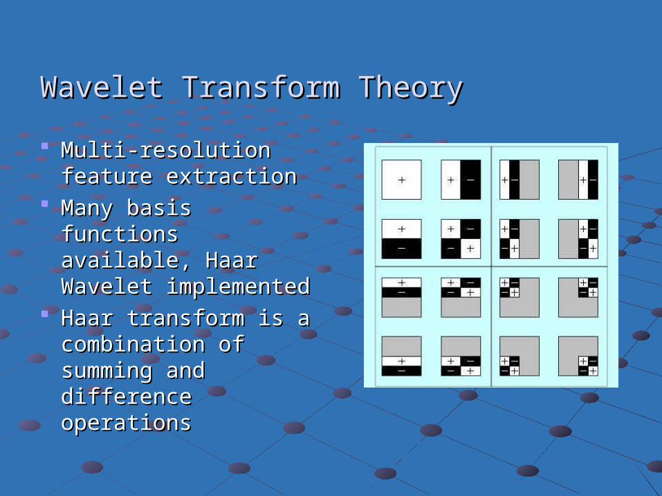
Wavelet Transform TheoryWavelet Transform Theory
Multi-resolution Multi-resolution feature extractionfeature extraction
Many basis functions Many basis functions available, Haar available, Haar Wavelet implementedWavelet implemented
Haar transform is a Haar transform is a combination of combination of summing and summing and difference operationsdifference operations

Hardware ImplementationHardware Implementation
Haar Transform can be realized as a Haar Transform can be realized as a Matrix Vector Multiplication problemMatrix Vector Multiplication problem
W (i,j) = ( ΣA(i)×P(i,j) ) × B(j) Multiply with either +1, 0 or -1Multiply with either +1, 0 or -1 Inputs are presented in bit-serial fashionInputs are presented in bit-serial fashion

System ArchitectureSystem Architecture
16 x 24 pixel array16 x 24 pixel array 2 CDS stages for 2 CDS stages for
inner and outer inner and outer productsproducts
Product coefficients Product coefficients input through shift input through shift registers registers
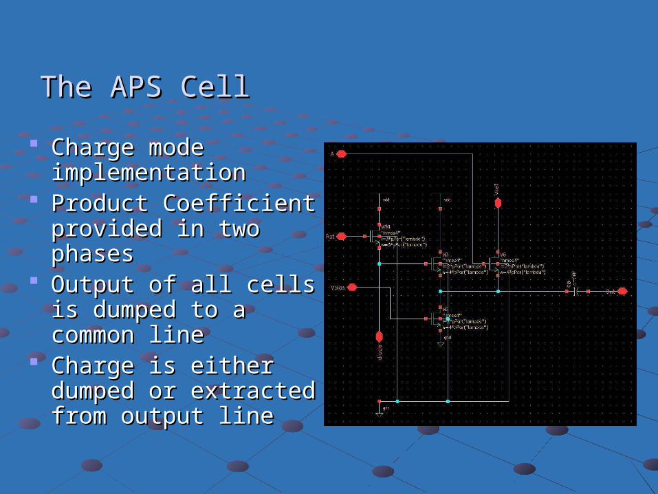
The APS CellThe APS Cell
Charge mode Charge mode implementationimplementation
Product Coefficient Product Coefficient provided in two phasesprovided in two phases
Output of all cells is Output of all cells is dumped to a common dumped to a common lineline
Charge is either Charge is either dumped or extracted dumped or extracted from output linefrom output line

The APS Cell (Layout)The APS Cell (Layout)
Uses photodiode type Uses photodiode type designdesign
Susceptible to Susceptible to mismatches in mismatches in transistor sizingtransistor sizing
Fill Factor: 60 %Fill Factor: 60 % Dimensions: 89Dimensions: 89λλ x x 8989λλ
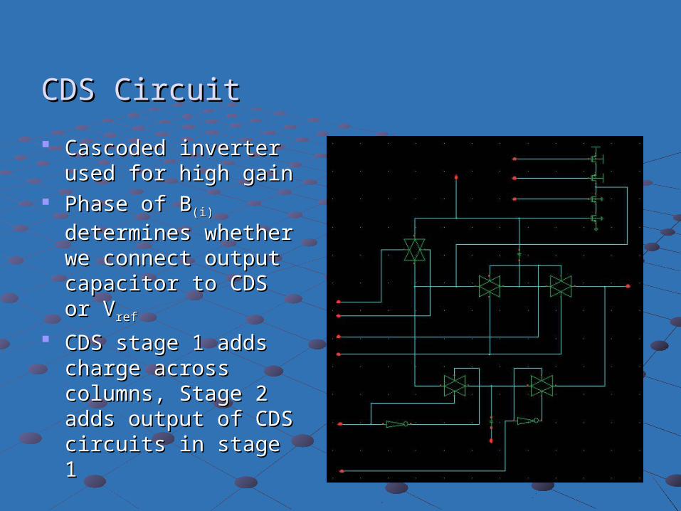
CDS CircuitCDS Circuit
Cascoded inverter Cascoded inverter used for high gainused for high gain
Phase of BPhase of B(i)(i)
determines whether determines whether we connect output we connect output capacitor to CDS or capacitor to CDS or VVrefref
CDS stage 1 adds CDS stage 1 adds charge across charge across columns, Stage 2 columns, Stage 2 adds output of CDS adds output of CDS circuits in stage 1circuits in stage 1

Complete Schematic Complete Schematic

Simulation of APS And Inner ProductSimulation of APS And Inner Product
Operating Operating Frequency of Frequency of 11KHz11KHz
Photocurrent of Photocurrent of 60pA60pA
Sequencing of 1Sequencing of 1stst and 2and 2ndnd stage stage clocks is very clocks is very importantimportant
Here we are Here we are multiplying by -1multiplying by -1

Simulation Results for Outer Product (4Simulation Results for Outer Product (4××4)4)
Here again we Here again we are multiplying are multiplying by -1by -1
Output valid Output valid during Hold during Hold phase of stage 2phase of stage 2
Voltage range of Voltage range of 1.76V to 4.23V, 1.76V to 4.23V, with reference at with reference at nearly 3 Vnearly 3 V

Complete Layout with Pad-frameComplete Layout with Pad-frame
Future workFuture work
Parallel readout (currently can be used as Parallel readout (currently can be used as a random-access imager)a random-access imager)
Extend for a 3 x 3 pad-frame. Would allow Extend for a 3 x 3 pad-frame. Would allow a resolution of around 72x72a resolution of around 72x72
More test pins. Currently the chip utilizes More test pins. Currently the chip utilizes 29 pins29 pins

QuestionsQuestions??