an electrical stimulus based built in self test (bist) circuit · 2013-10-08 · an electrical...
TRANSCRIPT

An Electrical Stimulus based Built In Self Test (BIST) circuit
for Capacitive MEMS accelerometer
by
Vinay Kundur
A Thesis Presented in Partial Fulfillment
of the Requirements for the Degree
Master of Science
Approved July 2013 by the
Graduate Supervisory Committee:
Bertan Bakkaloglu,Chair
Sule Ozev
Sayfe Kiaei
ARIZONA STATE UNIVERSITY
August 2013

i
ABSTRACT
Micro Electro Mechanical Systems (MEMS) is one of the fastest growing field in
silicon industry. Low cost production is key for any company to improve their market
share. MEMS testing is challenging since input to test a MEMS device require physical
stimulus like acceleration, pressure etc. Also, MEMS device vary with process and
requires calibration to make them reliable. This increases test cost and testing time. This
challenge can be overcome by combining electrical stimulus based testing along with
statistical analysis on MEMS response for electrical stimulus and also limited physical
stimulus response data. This thesis proposes electrical stimulus based built in self
test(BIST) which can be used to get MEMS data and later this data can be used for
statistical analysis. A capacitive MEMS accelerometer is considered to test this BIST
approach. This BIST circuit overhead is less and utilizes most of the standard readout
circuit. This thesis discusses accelerometer response for electrical stimulus and BIST
architecture. As a part of this BIST circuit, a second order sigma delta modulator has
been designed. This modulator has a sampling frequency of 1MHz and bandwidth of
6KHz. SNDR of 60dB is achieved with 1Vpp differential input signal and 3.3V supply.

ii
ACKNOWLEDGMENTS
First of all, I would like to express my appreciation and thanks to my supervisors
Dr. Bertan Bakkaloglu and Dr. Sule Ozev, for their support, guidance, and friendly
attitude during my graduate study and the development of this thesis. I would like to
thank my project mates Muhlis Kenan Ozel and Naveen Sai Jangala for their support,
great friendship and their helps.
I would like to present my special thanks to Freescale team Marie Burnam,
Tehmoor Dar, Ray Sessego, Ray Roop, Andrew McNeil, Mark Schlarmann, Jin Jo sung,
Peggy Kniffin, Bruno Debeurre, Mike Cheperak and many others for their invaluable
support during the course of this project.
Thanks to James Laux for his support in software and system issues. Thanks to all
my Professors whose courses helped me in enhancing my knowledge.
I would like to thank to my parents and my sister, for their patience, support, and
encouragement.
Lastly, I would like to thank all my classmates and friends for their support,
friendship and fun time.

iii
TABLE OF CONTENTS
Page
LIST OF TABLES ................................................................................................................... vi
LIST OF FIGURES ............................................................................................................... vii
CHAPTER
1 I NTRODUCTION ......................................................................................................... 1
1.1 BACKGROUND .......................................................................................................... 1
1.2 RESEARCH GOALS ................................................................................................... 1
1.3 CAPACITIVE MEMS ACCELEROMETER .................................................................... 3
1.3.1 Capacitive MEMS accelerometer structure .................................................... 4
1.4 PREVIOUS WORK ..................................................................................................... 6
1.5 SCOPE OF THIS THESIS ............................................................................................. 8
1.6 SUMMARY OF THIS CHAPTER ................................................................................... 8
2 SYSTEM LEVEL ANALYSIS, ARCHITECTURE AND MODELING ..................... 9
2.1 BIST REQUIREMENTS ............................................................................................... 9
2.2 MEASUREMENT TECHNIQUES ................................................................................ 10
2.2.1 Amplitude Response ..................................................................................... 10
2.2.2 Phase Response: ............................................................................................ 11
2.2.3 Offset Capacitance ........................................................................................ 12
2.3 ELECTRICAL STIMULUS .......................................................................................... 13
2.3.1 Electrical Stimulus to Self Test pin .............................................................. 14
2.3.2 Electrical Stimulus to Fixed sense plate ....................................................... 15
2.4 RESPONSE OF ACCELEROMETER TO ELECTRICAL STIMULUS ................................... 16

iv
CHAPTER Page
2.5 NOISE SOURCE IN CAPACITIVE ACCELEROMETER ................................................... 17
2.6 MODELING OF CAPACITIVE ACCELEROMETER ........................................................ 19
2.7 SYSTEM ARCHITECTURE ........................................................................................ 21
2.7.1 Typical Readout Circuit of MEMS accelerometer ....................................... 21
2.7.2 Readout Circuit with Built in Self Test(BIST) ............................................. 22
2.7.3 SNR Calculation ........................................................................................... 23
2.7.4 System Modeling in Simulink ...................................................................... 25
2.8 SUMMARY OF THIS CHAPTER .................................................................................. 27
3 SIGMA DELTA MODULATORS .............................................................................. 28
3.1 ADC REQUIREMENT .............................................................................................. 28
3.2 SIGMA DELTA MODULATORS ................................................................................. 29
3.3 OVERSAMPLING AND QUANTIZATION .................................................................... 31
3.4 NOISE SHAPING ...................................................................................................... 32
3.5 FILTERING AND DECIMATION ................................................................................. 35
3.6 OFFSET AND 1/F NOISE AND REDUCTION TECHNIQUES ........................................... 36
3.6.1 Correlated Double Sampling (CDS) ............................................................. 37
3.6.2 Chopper Stabilization.................................................................................... 38
3.7 SUMMARY OF THIS CHAPTER ................................................................................. 41
4 IMPLEMENTATION OF SIGMA DELTA MODULATOR ..................................... 42
4.1 SPECIFICATIONS FOR SIGMA DELTA MODULATOR: ................................................ 42
4.2 SIMULINK MODELING OF SIGMA DELTA MODULATOR .......................................... 45
4.2.1 Modeling Sampling clock Jitter .................................................................... 46

v
CHAPTER Page
4.2.2 Modeling Thermal Noise or KT/C ................................................................ 47
4.2.3 Modeling finite gain of amplifier in Integrators ........................................... 48
4.3 CIRCUIT IMPLEMENTATION .................................................................................... 49
4.3.1 Sampling Capacitors and switches ................................................................ 50
4.3.2 Integrator Amplifier: Requirements .............................................................. 51
4.3.2.1 Gain Requirement ..................................................................................... 51
4.3.2.2 Unity Gain Bandwidth and gm of Amplifier ............................................ 52
4.3.2.3 Slew Rate .................................................................................................. 54
4.3.2.4 Offset and 1/f noise reduction ................................................................... 54
4.3.3 Integrator Amplifier: Circuit and simulation Results ................................... 54
4.3.4 Common mode feedback circuit(CMFB) ..................................................... 57
4.3.5 Quantizer ....................................................................................................... 58
4.3.6 Non Overlapping clock generator ................................................................. 58
4.4 MODULATOR SIMULATION RESULTS ...................................................................... 60
4.5 MODULATOR LAYOUT ........................................................................................... 62
4.6 PERFORMANCE OF SIGMA DELTA MODULATOR IN OVERALL SYSTEM ..................... 63
4.7 SUMMARY OF THIS CHAPTER .................................................................................. 66
5 CONCLUSION AND FUTURE WORK .................................................................... 67
REFERENCES ................................................................................................................. 69

vi
LIST OF TABLES
Table Page
1 Categories of MEMS devices ......................................................................................... 1
2 Typical parameters of the accelerometer that was used ................................................ 20
3 Summary of Specifications for Sigma Delta Modulator ............................................... 44
4 Integrator Amplifier requirement .................................................................................. 54
5 Modulator summary ...................................................................................................... 66

vii
LIST OF FIGURES
Figure Page
1.1 Conceptual structure of Capacitive MEMS accelerometer (no acceleration) .............. 4
1.2 Conceptual structure of Capacitive MEMS accelerometer (with acceleration) ........... 5
1.3 Typical structure of on chip capacitive accelerometer [9] ........................................... 6
2.1 Algorithm to get amplitude response ......................................................................... 10
2.2 Algorithm to get 900 phase shift frequency ............................................................... 12
2.3 Accelerometer structure with offset ........................................................................... 13
2.4 Simplified accelerometer structure with self test finger (xyz_st) .............................. 15
2.5 Simplified block diagram showing stimulus and readout from fixed plates ............ 16
2.6 Electrical Stimulus and Response voltage of accelerometer ..................................... 17
2.7 Spring mass Damper system ...................................................................................... 19
2.8 Magnitude and Phase response of the accelerometer from the transfer function using
typical values .................................................................................................................... 21
2.9 Block Diagram of typical MEMS accelerometer readout circuit .............................. 21
2.10 Accelerometer readout circuit with DAC for electrical stimulus ............................ 23
2.11 Detailed block diagram of our BIST and Readout .................................................. 23
2.12 BIST system modeling in simulink ......................................................................... 25
2.13 Implementation of electrical stimulus voltage to acceleration ................................ 25
2.14 Switched Capacitor C2V architecture assumed for System Level analysis [14] ..... 26
2.15 PSD at C2V output................................................................................................... 27
2.16 PSD at Modulator output ......................................................................................... 27
3.1 Typical performance of different ADC [15] .............................................................. 29

viii
Figure Page
3.2 Block diagram of the delta modulator structure. ....................................................... 30
3.3 Block diagram of Sigma – Delta modulator (a) with two integrators (b) with the
integrator blocks combined into one. ................................................................................ 31
3.4 Block diagram of the sigma – delta modulator in s-domain, with the quantization
error ................................................................................................................................... 33
3.5 Noise response of various order sigma – delta modulators ....................................... 34
3.6 In band quantization noise of sigma – delta modulators, depending on the
oversampling ratio and modulator order [19] ................................................................... 34
3.7 (a) Input signal, (b) output of the modulator with the quantization noise, (c) low pass
filtration, (d) low pass filtered & decimated output. ......................................................... 35
3.8 PSD of 1/f noise of CMOS ........................................................................................ 36
3.9 Correlated double sampling techniques [20] ............................................................. 37
3.10 Chopper Stabilization technique [20] ...................................................................... 39
3.11 Baseband Spectrum .................................................................................................. 40
4.1 Comparison of Noise from different components at ADC input ............................... 43
4.2 Generic Second order modulator (CIFB) [22] ........................................................... 45
4.3 Modulator block diagram with Coefficients .............................................................. 45
4.4 Simulink Model of Second order Sigma Delta modulator with non-idealities .......... 46
4.5 PSD at simulink modulator output (SNDR=59.4dB over 12KHz) ............................ 46
4.6 Simulink Model: Effect of Sampling clock jitter on signal ....................................... 47
4.7 KT/C noise modeling ................................................................................................. 48
4.8 Effect of finite gain of integrator amplifier on NTF ( noise shaping) ....................... 49

ix
Figure Page
4.9 Modeling of Non ideal integrator .............................................................................. 49
4.10 Second Order Sigma Delta Modulator ..................................................................... 50
4.11 NTF for different amplifier gain compared with input signal noise ........................ 52
4.12 Loading condition of integrator amplifier in 2 clock phases ................................... 53
4.13 Folded cascode amplifier ......................................................................................... 55
4.14 Gain and phase plot of folded cascode for two load conditions ( solid line: 200fF.
dotted line:800fF).............................................................................................................. 55
4.15 Folded cascode Amplifier with chopper switches ................................................... 56
4.16 Chopper modulator and demodulator ...................................................................... 57
4.17 Switched capacitor CMFB ....................................................................................... 57
4.18 One Bit Quantizer .................................................................................................... 58
4.19 Non overlapping clock generator ............................................................................. 59
4.20 Non overlapping clock phases ................................................................................. 59
4.21 Modulator input referred noise with and without chopping .................................... 60
4.22 Comparison of ADC thermal noise, quantization noise, input signal noise and total
noise .................................................................................................................................. 61
4.23 PSD at modulator output for 1Vpp differential input ( Post layout R+C+CC netlist)
........................................................................................................................................... 61
4.24 Modulator SNDR with input signal power .............................................................. 62
4.25 Sigma Delta modulator layout snapshot .................................................................. 63
4.26 Signal readout chain ................................................................................................. 63
4.27 PSD at Modulator input(frond end output) with entire signal chain ....................... 64

x
Figure Page
4.28 PSD at modulator output with entire signal chain ................................................... 65

1
Chapter 1 Introduction
1.1 Background
Micro Electro Mechanical Systems (MEMS) convert mechanical signal into an
electrical signal. MEMS components available in market can be broadly divided into six
categories[1].
Table 1 Categories of MEMS devices
Product Category Examples
Pressure Sensors Manifold pressure(MAP),tire pressure, blood pressure
Inertia sensor Accelerometers, gyroscope, crash sensor..
Microfluidics/bioMEMS
inkjet printer nozzle, micro bio analysis systems, DNA
chips
optical MEMS micro grating array for projection (DLP), adaptive optics
RF MEMS High Q inductors, switches, antenna, filter
others relays, microphones, data storage, toys
Freescale, Analog Devices, ST Microelectronics, Robert Bosch, Texas Instruments etc
are some of the key players in MEMS manufacturing.
Since, these MEMS devices are widely used in lot of application, Reliability and
production cost have become a key parameter for companies to gain market share in this
competitive market.
1.2 Research Goals
There are various tough challenges in achieving low-cost MEMS production.
MEMS manufactured devices exhibit increasingly high process variations,
making calibration and compensation necessary at every manufacturing step.

2
MEMS devices are generally associated with low yield. However, there are few
known techniques to screen the devices for defects at the wafer level [2].
ATE testing and calibration of packaged units require special handlers and
application of a multi-axis physical stimuli including shaking, flipping, which
increases the testing cost.
Existing approaches for MEMS testing are based on conducting limited electrical
testing at wafer level and using precision physical stimulus based testing after packaging.
The physical stimuli include light, audio, pressure, magnetic, velocity and acceleration,
which increases the device level measurement noise floor, and test cost. As an example,
in the case of pressure sensing, the challenge is to relate the motional EMF on surfaces
from electrical forces to the electromotive forces of pressure, while including the effects
such as packaging to obtain a carefully calibrated device. It has been shown for various
types of sensors that electrical stimulation can be used to facilitate lower cost
calibration[3].
The ultimate goal of this research is to develop a unified framework for
characterization, calibration, and testing of MEMS devices using on-die electrical
structures, enhanced electrical readings from the device under test using ATE level and
built-in-self-test circuitry, with minimum or no physical stimuli.
In order to facilitate this low-cost testing and characterization process, this
research is focused on the following three subjects:
A. using a statistical framework that relates process parameters to electrical stimuli
response at the wafer level for process feedback and wafer-level test compaction.

3
B. Designing information-rich, spectral and time domain test signals so that the
MEMS devices can be excited electrically.
C. Designing on-chip and off-chip circuitry to facilitate the data collection and
processing during wafer-level and final production testing, enabling low-cost
testers for complex spectral characterization .
Reference [3] gives detailed background about this approach.
A capacitive MEMS accelerometer has been chosen to test our BIST idea in this
project. Later this idea will be extended to other MEMS devices. From now on,
capacitive MEMS accelerometer is referred to as just MEMS for simplicity unless
otherwise mentioned.
1.3 Capacitive MEMS accelerometer
The first micro machined accelerometer was designed in 1979 at Stanford
University, but it took over 15 years before such devices became accepted mainstream
products for large volume applications [4].
Accelerometer converters acceleration to proportional electrical signal. Capacitive
MEMS accelerometers are widely used in portable electronics for tilt detection, GPS
augmented navigation, Earthquake detection, micro gravity measurement in space, bio
medical application and oil exploration [5] [6]. With the development of Micro electro
mechanical systems (MEMS) and the improvement of commercial value of
accelerometer, capacitive MEMS accelerometers have become an increasingly
emphasized point in the region of MEMS and micro sensors for their high sensitivity, low
temperature sensitivity, low power consumption, wide dynamic range of operation and
simple structure[7].

4
1.3.1 Capacitive MEMS accelerometer structure
Conceptual structure of capacitive MEMS accelerometer is given in Figure 1.1
Figure 1.1 Conceptual structure of Capacitive MEMS accelerometer (no acceleration)
Typical MEMS accelerometer consists of a movable mass attached to a fixed
structure through spring. Capacitance is formed between movable mass and fixed fingers
as shown in Figure 1.1. Whenever there is acceleration, movable mass moves from its
rest position and changes the capacitances C.
C capacitance is given by
Equation 1.1
where
ε0 = permittivity of free space = 8.854x10⁻¹²
m-3
kg-1
s4A
2
εr = relative permittivity = 1 (for free space)
A = overlap area
d = distance between plates

5
In presence of acceleration, accelerometer structure is shown below
Figure 1.2 Conceptual structure of Capacitive MEMS accelerometer (with acceleration)
Assume that, movable mass moves by distance x because of force. Then, top and
bottom capacitances will change. This can be given by[8]
Equation 1.2
Equation 1.3
We can define
Equation 1.4
When x is small compared to d, then Equation 1.4 can simplified and re-arranged as
Equation 1.5
For a spring mass system, acceleration (a) can be written as
Equation 1.6

6
using Equation 1.5 in Equation 1.6
Equation 1.7
Equation 1.7 shows that acceleration is directly proportional to cap variation C. If we
can measure this cap variation, then acceleration can be measured. To improve the
readability of this cap variation, multiple caps in the form of comb are used. This is
shown in Figure 1.3.
Figure 1.3 Typical structure of on chip capacitive accelerometer [9]
1.4 Previous Work
A built-in self test technique for MEMS that is applicable to symmetrical
microstructures is described in [9]. A combination of existing layout features and
additional circuitry is used to make measurements from symmetrically-located points. In

7
addition to the normal sense output, self-test outputs are used to detect the presence of
layout asymmetry that are caused by local, hard-to-detect defects. Simulation results for
an accelerometer reveal that this self test approach is able to distinguish misbehavior
resulting from local defects and manufacturing process variations.
In [10], A built-in self-test (BIST) scheme which partitions the fixed (instead of
movable) capacitance plates of a capacitive MEMS device is proposed. The BIST
technique divides the fixed capacitance plate(s) at each side of the movable
microstructure into three portions: one for electrostatic activation and the other two equal
portions for capacitance sensing. Due to such partitioning, the BIST technique can be
applied to surface-, bulk-micro machined MEMS devices and other technologies.
[11] discusses an approach which allows testing of the device by electrostatic
deflection of the mass. Even though the spring constants of the device may vary from unit
to unit or over temperature and even though the piezo resistive coefficients vary over
temperature, as long as the electrostatic voltage and initial separation gap are held
constant, the output will be proportional to a given acceleration. Applications of this
technology are in temperature compensation, testability, and uni-directional force-balance
applications. On chip test Signal generation Technique proposed in [12] requires only
slight modifications and allows a production test of the imager with a standard test
equipment, without the need of special infrared sources and the associated optical
equipment. The test function can also be activated off-line in the field for validation and
maintenance purposes.

8
1.5 Scope of this Thesis
To achieve the goal of low cost MEMS testing, we need the BIST circuit which
can read the MEMS data, needed for statistical analysis and get the calibration
coefficients. This thesis focuses on following things
a. Development of BIST architecture which gives little or no overhead in terms of
circuit area.
b. Behavior of MEMS accelerometer for electrical stimulus
c. Circuit modes to get different parameters of MEMS accelerometer device.
d. Performance requirement of circuit blocks
e. System level analysis and planning.
f. Development of sigma delta modulator for readout circuit.
1.6 Summary of this Chapter
1. Reducing the test cost of MEMS is one of the key factors for achieving higher
share in this competitive market.
2. Electrical stimulus based BIST is one approach to reduce the test cost.
3. MEMS capacitive accelerometer is used to test our idea.
4. Typical structure of capacitive MEMS accelerometer is discussed
5. This thesis focuses on development of BIST circuit.

9
Chapter 2 System Level Analysis, Architecture and Modeling
This chapter focuses on following things
BIST requirements
Electrical stimulus for accelerometer and its response
Noise sources in accelerometer
Accelerometer modeling
Readout circuit along with BIST and its modeling
SNR calculations and simulation results from simulink model
2.1 BIST requirements
To do the statistical correlation analysis mentioned in section 1.2, in BIST, we
need accelerometer response which depends on its parameters like Spring constant(k),
offset capacitance( Coffset),mass(m), damping factor(ζ) etc. With this BIST approach, we
are not trying to measure the exact values of accelerometer parameters. Accelerometer
response is needed for statistical analysis only.
Reference [3] shows that for good statistical correlation data, among different
MEMS samples , we need amplitude response, phase response (i.e Bode plot) and offset
capacitance of MEMS. Main aim of our BIST is to capture these parameters (frequency
response, phase response and offset capacitance of MEMS).
MEMS readout circuit will have circuit to measure the response for physical
stimulus also. To reduce BIST circuit overhead, we need to reuse as many blocks as
possible from this standard readout. In summary, Readout circuit should handle MEMS
response for both physical stimulus and electrical stimulus.

10
2.2 Measurement Techniques
As mentioned in previous section, we need the following accelerometer data for
accurate statistical correlation analysis
Amplitude response
Phase response
Offset capacitance
All of this are done as a part of BIST in other words MEMS response to electrical
stimulus.
2.2.1 Amplitude Response
Amplitude response of a system is a plot of output amplitude of a system for
different input frequencies. Input signal must be sinusoidal. To measure this response, we
need to stimulate accelerometer with sinusoidal electrical signal. Accelerometer is
stimulated with on-chip/off chip sinusoid with a given frequency, and amplitude is
measured and stored. Next, frequency will be changed and process is repeated..
Algorithm for getting amplitude response is given below.
Figure 2.1 Algorithm to get amplitude response
START
Stimulate MEMS with sinusoidal
signal with frequencies from 1KHz
to 6KHz in steps of 500Hz
Measure the output amplitude
Store the output amplitude
corresponding to each frequency

11
2.2.2 Phase Response:
Phase response of a system is a plot of phase shift from input to output for
different input frequencies. Input signal must be sinusoidal. To measure this response, we
need to stimulate MEMS with sinusoidal electrical signal.
In Phase response, we are particularly interested in 900 phase shift point. This
frequency is the natural frequency of MEMS. To extract this information, we can
multiply input and output.
At 900 phase shift point, multiplier(mixer) output DC value will be zero.
To illustrate this, let
Equation 2.1
If MEMS produces phase shift of θ, output can written as
Equation 2.2
Output amplitude and input amplitude can be different because of MEMS
Product = input X output = Asin(ωt) X Bsin(ωt + θ)
= 0.5 AB [ cos(ωt - ωt - θ) - cos(2ωt + θ) ]
Equation 2.3
The above product has a DC component with magnitude 0.5 AB.cos(θ).When phase shift
is 90 deg, i.e θ = 900, then DC component 0.5ABcos(θ) = 0. For all other phase shifts,
there will be DC component associated with product.
For the above method to work, we have to make sure that signals that we are
multiplying, have same frequency. Usually, accelerometer output frequency will be twice

12
the electrical input stimulus frequency. So, double the input frequency must be multiplied
with output.
Algorithm for getting phase response is given in Figure 2.2.
Figure 2.2 Algorithm to get 900 phase shift frequency
2.2.3 Offset Capacitance
In an accelerometer, capacitance is formed between fixed plates and movable
mass as shown in Figure 2.3.
START
Stimulate MEMS with sinusoidal
signal with frequencies from 1KHz
to 6KHz in steps of 500Hz
Multiply 2X frequency of input
and output
Store the multiplier output
corresponding to each frequency
multiplier output with zero DC is the
90 deg phase shift point

13
Figure 2.3 Accelerometer structure with offset
The capacitors C1 and C2 will be different due to mismatch in gaps or width of
plates and this causes voltage offset in the electrical signal. This creates errors when
detecting constant acceleration. To measure this offset, we have to read the electrical
signal out of this MEMS without any physical or electrical stimulus. Then the output
electrical signal will be proportional to rest capacitance difference C1-C2 which is the
offset.
2.3 Electrical Stimulus
Voltage difference between fixed plate and movable mass creates force that
moves the movable mass.
The Force(F) between 2 plates is given by [11]
Equation 2.4
Where,
A = overlap area between fixed plate and movable mass
V = voltage difference between fixed plate and movable mass
d = distance between fixed plate and movable mass

14
This force is independent of polarity of voltage and is always attractive force ( No
repulsion force). For our accelerometer in Figure 2.3,
Let V1 = voltage on top plate X1
V2 = voltage on bottom plate X2
Let voltage on movable mass be 0.
Then, Net force on movable mass will be difference of forces from each fixed plates
Equation 2.5
In other words, if we apply same voltage to plates X1 and X2, then movable mass
will not move at all ( assuming equal gap).
There are 2 options to give Electrical Stimulus signal to accelerometer.
1. To Self test pin
2. To one of the fixed plate.
Both of these option are discussed next.
2.3.1 Electrical Stimulus to Self Test pin
In the accelerometer comb structure, few fixed fingers are used for self test ( also
called actuation fingers) to electrically stimulate the accelerometer and move the movable
mass as shown in Figure 1.3. Simplified structure is shown in Figure 2.4.

15
Figure 2.4 Simplified accelerometer structure with self test finger (xyz_st)
Advantage of using a separate pin for electrical stimulus is that signal can be read
differentially. This is good from circuit design point of view. But, overlap area between
self test pin (xyz_st) and movable mass is small. This produces small force and
capacitance variation will be too small to detect over stimulus signal frequency range for
amplitude response.
In our accelerometer, Overlap area between self test pin and movable mass is
nearly 1/10th of the overlap area between fixed sense plates and movable mass. So, force
, in case of self test, will be 1/10th of force when stimulus is applied to fixed sense plate.
2.3.2 Electrical Stimulus to Fixed sense plate
Since overlap area between fixed sense plate and movable mass is large, we use
this fixed sense plate for stimulation. This approach gives more cap variation than
previous approach. Simplified structure is shown in Figure 2.5.
16
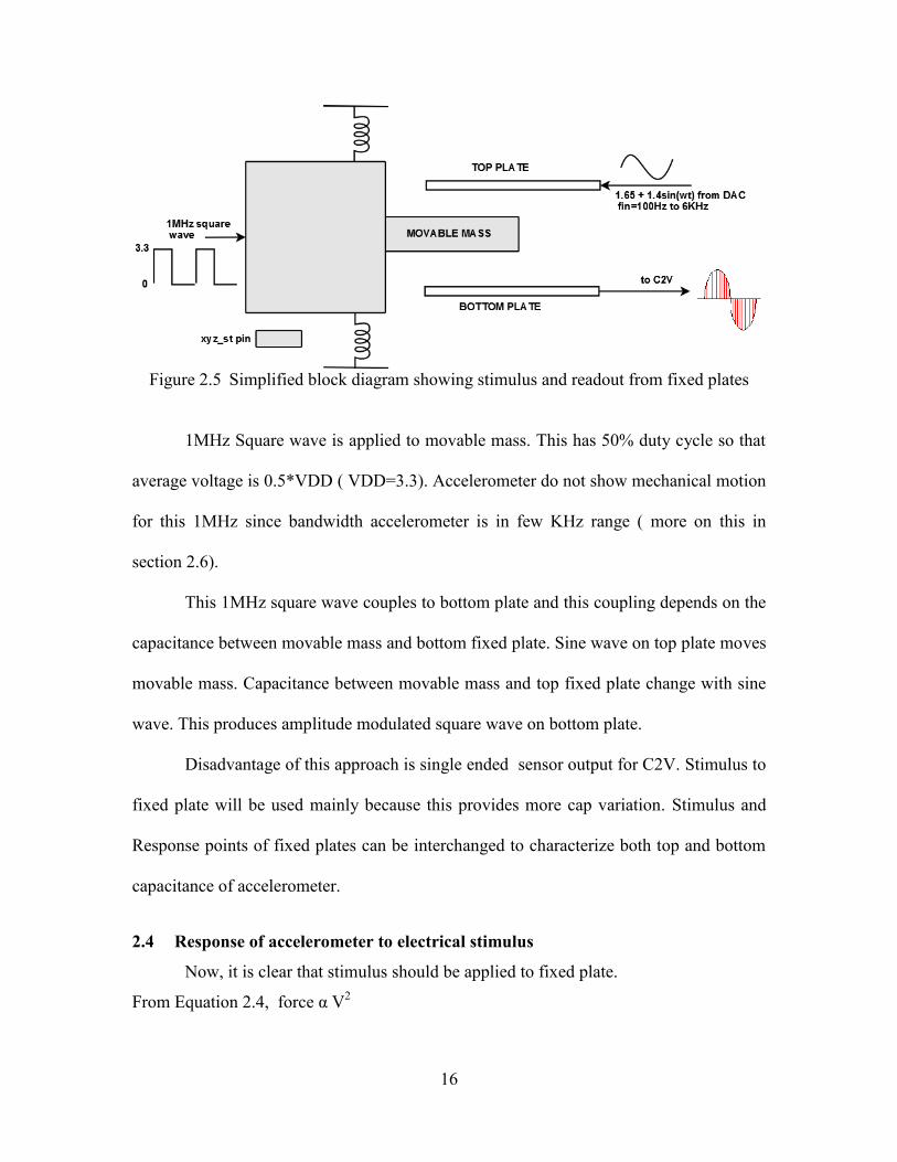
Figure 2.5 Simplified block diagram showing stimulus and readout from fixed plates
1MHz Square wave is applied to movable mass. This has 50% duty cycle so that
average voltage is 0.5*VDD ( VDD=3.3). Accelerometer do not show mechanical motion
for this 1MHz since bandwidth accelerometer is in few KHz range ( more on this in
section 2.6).
This 1MHz square wave couples to bottom plate and this coupling depends on the
capacitance between movable mass and bottom fixed plate. Sine wave on top plate moves
movable mass. Capacitance between movable mass and top fixed plate change with sine
wave. This produces amplitude modulated square wave on bottom plate.
Disadvantage of this approach is single ended sensor output for C2V. Stimulus to
fixed plate will be used mainly because this provides more cap variation. Stimulus and
Response points of fixed plates can be interchanged to characterize both top and bottom
capacitance of accelerometer.
2.4 Response of accelerometer to electrical stimulus
Now, it is clear that stimulus should be applied to fixed plate.
From Equation 2.4, force α V2

17
So, if stimulus voltage V = Asin(ωt) then
Equation 2.6
Frequency of the response will be twice the Electrical stimulus frequency. For
example, if we want a mechanical movement at 1KHz then electrical stimulus signal
should be at 500Hz. We can imagine accelerometer output like a rectifier output as
shown below.
Figure 2.6 Electrical Stimulus and Response voltage of accelerometer
2.5 Noise Source in capacitive accelerometer
Brownian noise is thermal-mechanical noise. It creates a random force with Brownian
motion of air molecules caused by damping and is directly applied to seismic mass. The
power spectral density (PSD) of the Brownian noise force is shown in Equation 2.7
Equation 2.7
Where,
FB = Brownian noise force in N2/Hz
KB= Boltzmann's constant

18
T=Temperature
b= Damping co-efficient =
ζ = Damping factor of the movable mass
k = spring constant of the movable mass
m=mass of the movable mass
From Equation 2.7, we can note that higher damping factor lead to more
Brownian noise. For low noise, low damping factor is needed. But, low damping factor
makes MEMS accelerometer under-damped and movable mass takes more time to settle.
This Brownian noise has zero mean and FB2
variance.
It is more meaningful to represent noise in terms of acceleration. So, Brownian
noise in terms of acceleration can be represented as
Equation 2.8
In our case, T= 300K
ζ = 0.7
k= 3.5 N/m
m=3.3n Kg
So, Damping co-efficient b= 150.45u
Equating these values in Equation 2.8 gives
Equation 2.9
OR
Equation 2.10

19
Equation 2.8 is interesting to observe as the smaller device size (i.e smaller mass)
reduces the signal to noise ratio [13]. Intuitively this may be understood by noting that
ratio of mechanical to thermal energy E/kT goes down as the device mass is reduced.
This limits the shrinking of mechanical devices on silicon wafer[13].
2.6 Modeling of Capacitive accelerometer
The accelerometer can be modeled as a basic mass spring damper system as
shown in Figure 2.7
Figure 2.7 Spring mass Damper system
For an external acceleration of a applied to the sensor, the equations of motion can be
shown as in Equation 2.11.
Equation 2.11
In this equation x is the displacement of the proof mass according to a reference frame
placed on the body of the accelerometer, where the electrodes and the anchor points are
fixed. The Laplace transform of the equation gives Equation 2.12
Equation 2.12

20
Transfer function can be written as
Equation 2.13
comparingTransfer function can be written as
Equation 2.13
Equation 2.13 to generic second order transfer function we can get resonance
frequency(ω0) and the quality factor(Q) of the accelerometer as follows
Equation 2.14
Equation 2.15
. Table 2 Typical parameters of the accelerometer that was used
Parameter Value Unit
Mass(m) 3.3n Kg
Spring
Constant(k)
3.5 N/m
Area(A) 60n m2
Gap(d) 1.7u m
Damping factor(ζ) 0.7
Typical parameter values of accelerometer that we used are shown in Table 2.
Using these values , bode diagram is plotted for Equation 2.13 in Figure 2.8.
The magnitude of the accelerometer response is almost constant in the frequency
band below the resonance frequency.. Hence, the accelerometer is operated in this linear

21
region for acceleration detection. As the quality factor is increased, the peak at the
resonance frequency increases, which is the case generally obtained if the mechanical
sensor is operated in vacuum environment.
Figure 2.8 Magnitude and Phase response of the accelerometer from the transfer function
using typical values
2.7 System Architecture
2.7.1 Typical Readout Circuit of MEMS accelerometer
Typical readout circuit of MEMS accelerometer consists of Charge to voltage(C2V)
converter, Gain stage and ADC as shown Figure 2.9.
Figure 2.9 Block Diagram of typical MEMS accelerometer readout circuit
MEMS accelerometer is excited physically or electrically. This changes the
capacitance of MEMS accelerometer. Capacitance variation changes the charge stored in

22
those caps. This charge variation is detected by Charge to voltage (C2V) converter and
converted to voltage. This C2V can be switched cap or continuous time circuit depending
on application. Some of the popular C2V architectures are[14]
1. AC bridge with voltage amplifier
2. Trans-impedance amplifier
3. Switched capacitor circuit
4. Switched capacitor circuit with KT/C noise reduction
Accelerometer capacitance variation will be small compared to rest capacitance.
Typically, peak variation of 5-10 fF on top of 0.5 to 1 pF. This makes design of C2V a
challenge.
Once C2V gives voltage this can be converted to digital form using ADC. But,
this voltage will be small. To improve the dynamic range of ADC, a gain stage placed
between C2V and ADC. This gain can be programmable depending upon need.
Finally, an ADC is placed this converts the voltage to digital form. This can be used by
DSP.
2.7.2 Readout Circuit with Built in Self Test(BIST)
In BIST, we stimulate the accelerometer with electrical stimulus. This electrical
stimulus is sine wave. A circuit is needed to generate this sine wave. After accelerometer
is stimulated with sine wave, readout method will be same as with a physical stimulus.
For Readout circuit, physical stimulus or electrical stimulus do not matter.
One of the way to implement sine wave generator is using DDFS+DAC. This
generates stepped sine wave. This can be used for stimulus. With this approach only
additional circuit will be DDFS+DAC. Circuit overhead will be less.

23
Readout circuit with DAC is shown in Figure 2.10
Figure 2.10 Accelerometer readout circuit with DAC for electrical stimulus
Since, aim of this research is to test the concept of statistical correlation with
these BIST circuit, most of the digital blocks will be implemented off chip. Main digital
blocks are DDFS and Decimation filter of ADC.
Our accelerometer is a 3 axis accelerometer. So, we need mux to select the axis. A more
detailed block diagram is given in Figure 2.11
Figure 2.11 Detailed block diagram of our BIST and Readout
2.7.3 SNR Calculation
Referring to Figure 2.5 If we apply voltage V to fixed plate w.r.t movable mass, then
movable mass experiences force
where d is the gap between movable mass and fixed plate in rest position.

24
Due to force, if movable mass moves by x towards fixed plate then force changes to
Equation 2.16
If we express this force in acceleration, then
Equation 2.17
So, acceleration due to electrical stimulus experienced by movable mass changes with the
displacement dynamically. This makes analysis really complex if want to consider this
acceleration variation because of displacement change.
To simplify things, we can take x << d. This is the practical case to make the
operation of accelerometer linear. In our case x~5nm while d~1.7um. This can be
approximately calculated from Equation 2.13 and table 2. This gives acceleration to be
Equation 2.18
From values in Table 2 and we using 1.3sin(ωt) as stimulus. So, this gives V=1.3V.
Equating these things in Equation 2.18. We get a = 4.8 g of acceleration. This is peak
acceleration. RMS will be 0.707*a
Equation 2.19
From Equation 2.10, we found that noise is ~49ug/sqrt(Hz).
If we use 12KHz integration bandwidth, then noise acceleration (G n) will be
Equation 2.20
Now we can calculate SNR.
Equation 2.21

25
This is the SNR calculated from Brownian noise of acceleration only. This does
not include substrate noise or circuit noise. So, 56dB is the best SNR that we can get.
This is the input referred SNR.
2.7.4 System Modeling in Simulink
Simulink model was done to emulate the functioning of BIST circuit. Simulink
model is shown below.
Figure 2.12 BIST system modeling in simulink
This simulink model is the implementation of Figure 2.10. Stimulus for BIST will
be stepped sine wave. This voltage is converted to acceleration in the 'voltage to
Acceleration' block. This block implements Equation 2.18. Implementation of this block
is shown in Figure 2.13.
Figure 2.13 Implementation of electrical stimulus voltage to acceleration

26
This block gives acceleration output. This acceleration displaces the movable mass as
transfer function given in Equation 2.13 . 'Acceleration to Displacement' block
implements this transfer function. Displacement in movable mass lead to capacitance
variation as shown in Equation 1.4. This capacitance is detected by C2V and gives output
voltage. Transfer function of capacitance variation to voltage is given by [14] for
switched cap architecture of C2V
Figure 2.14 Switched Capacitor C2V architecture assumed for System Level analysis[14]
Equation 2.22
If we use 3.3V supply, then Vpeak=3.3. Cfb = 300fF is assumed. This is close to the rest
cap of accelerometer. Also, gain can be placed after C2V to improve the dynamic range
of ADC. A Sigma delta architecture is used for ADC.
Spectral density at the output of C2V is shown in Figure 2.15. SNR of 42dB is
observed at the output of C2V. Ideally, ADC should not degrade this SNR. Spectral
density at the output of modulator is shown in Figure 2.16. SNR of 42dB is observed at
modulator output. This indicates that modulator is not affecting the input SNR. Noise
floor at modulator is same as input signal noise floor. System level analysis includes
thermal noise of C2V and ADC.

27
Figure 2.15 PSD at C2V output
Figure 2.16 PSD at Modulator output
2.8 Summary of this chapter
In this chapter modeling of accelerometer ( transfer function, noise) is explained.
The BIST architecture and its requirements are also covered. A simulink model of BIST
based on transfer functions is created and an SNR of 42dB is observed.
SNR = 42dB
SNR = 42dB

28
Chapter 3 Sigma Delta Modulators
This chapter discusses following things
ADC architecture choice
General theory of sigma delta modulator
Offset and 1/f noise reduction techniques
3.1 ADC Requirement
An ADC is needed to convert the voltage signal generated by C2V to digital
signal. Noise in signal chain is dominated by first few stages. In our case, overall noise is
dominated by C2V and Gain stage, as these stages come before ADC as shown in Figure
2.10. Our Signal readout circuits are switched capacitor circuits operating at 1MHz. To
synchronize the signal transfer between C2V and ADC, same sampling frequency(1MHz)
must be used. If we do not use same sampling frequency for C2V and ADC, then AAF
and voltage buffers must be used between C2V and ADC. This takes more area and extra
effort to make those circuits. So, better choice is to use same sampling frequency for C2V
and ADC. And, this fixes ADC sampling rate(Fs) to 1MHz. Section 2.3 to 2.6 shows that
accelerometer is physically stimulated up to 6KHz. So, maximum input signal
frequency(BW) will be 6KHz. Over Sampling ratio (OSR) can be gives as
Equation 3.1
As already mentioned, C2V noise dominated the read chain noise and it is enough
if we keep ADC noise below the input signal noise floor so that ADC does not degrade
the signal SNR. Input signal SNR is close to 42dB as predicted in section 2.7.4. This is

29
equivalent of 7 bit accuracy. Now we know the ADC requirement to some extent and we
have to decide the architecture.
Figure 3.1 Typical performance of different ADC[15]
Figure 3.1 shows typical performance of some of the widely used ADC
architectures. In our case sampling rate is 1MHz and ENOB is 7 bit. This puts us in
region indicated as white star in Figure 3.1.
This gives following architectural choices
1. Folding ADC
2. Sigma Delta Modulator
To maximize SNR for high OSR as in our case, sigma delta ADC are good
choice. Also, component matching requirement in Sigma delta is not stringent compared
to Folding ADC. Sigma delta ADC typically do not require any external components [16]
3.2 Sigma Delta modulators
Sigma-delta modulation was developed from delta modulation [17]. Delta
modulation is an A/D conversion technique, where the output is quantized according to

30
how fast the input signal amplitude varies. Hence, if the output is 1-bit, the bit stream at
the output indicates only the sign of the variations of the input signal. Figure 3.2 shows
the basic block diagram of a delta modulator. Integrator in the feedback loop is trying to
predict the input signal and an error signal is generated after taking the difference
between the prediction and the input signal. This error signal is then quantized using a
comparator. Depending on the sign of the error signal, another prediction is made by
increasing or decreasing the value at the output of the integrator. On the demodulation
side, the 1-bit output stream should be integrated to obtain the quantized signal. Then,
with the use of a low-pass filter, the analog input signal can be regenerated.
Figure 3.2 Block diagram of the delta modulator structure.
The operations performed in this system are linear, so the integrator stage at the
demodulator can be carried to the input stage, as shown in Figure 3.3(a). Moreover, in the
block diagram in Figure 3.3(b), the two integrators are combined into one integrator. This
structure forms the first order sigma-delta modulator. In this structure, the output is
directly dependent on the input signal; hence, the demodulator side only needs a low-pass
filter. The operation is also performed using a single integrator on the modulator side;
hence, it is much simpler than the delta modulator structure. The output of a sigma-delta

31
modulator is commonly single bit; the resolution in amplitude is carried to the resolution
in time, which is achieved by oversampling.
Figure 3.3 Block diagram of Sigma – Delta modulator (a) with two integrators (b) with
the integrator blocks combined into one.
The sigma-delta A/D converters are widely used for high resolution and low bandwidth
applications due to the noise shaping and oversampling techniques. Oversampling sigma-
delta modulators are extensively used for low frequency analog-to-digital converters
especially in audio applications where the over-sampling ratio can be considerably high
and the noise rejection is very efficient [18].
3.3 Oversampling and Quantization
Oversampling is a crucial concept in sigma–delta modulators in order to increase the
resolution of the system by increasing the sampling frequency of the system.
Oversampling increases the resolution in the time domain, and decreases the in-band
noise. The Nyquist rate A/D converters have a sampling rate twice the bandwidth of the
signal frequency; but the oversampling converters use higher sampling rates. The
oversampling ratio is defined as in Equation 3.1.

32
Quantization and the error caused by quantization is a significant point, which should be
considered primarily in an A/D system. In Nyquist sampling quantizers, the rms value of
the error is given as in Equation 3.2 [19]
Equation 3.2
where, is the quantization level spacing. Hence the quantization error is bounded
between /2 and - /2, and have equal probability of taking any value in between. If there
is a dither signal, with sufficiently large in amplitude, the quantization error can be
assumed to be a white noise [19]. Using this assumption, for an oversampling quantizer,
the noise power inside the signal bandwidth is given as in Equation 3.3.
Equation 3.3
Conceptually, oversampling provides resolution in time, instead of resolution in
amplitude. By decimation process, the high-resolution result can be obtained. However,
as can be observed from the quantization noise expression given in Equation 3.3.
doubling the sampling frequency results only a 3 dB enhancement in the quantization
noise. Therefore, oversampling by itself does not improve the resolution of the system as
desired. The sigma-delta modulation, not only does oversampling but also the noise
shaping, which decreases the in-band quantization error considerably.
3.4 Noise Shaping
Noise shaping concept is the major purpose of usage of sigma-delta modulation. For a
first order sigma-delta modulator, the quantization error is added in the last stage, where
analog data is converted to digital, as shown in Figure 3.4

33
Figure 3.4 Block diagram of the sigma – delta modulator in s-domain, with the
quantization error
The transfer function of the system can be calculated as given in Equation 3.4.
which results in a low pass filter characteristic. For calculating the transfer function from
input to output, the quantization noise is taken to be zero.
Equation 3.4
For calculating the noise transfer function, input signal X(s) is assumed zero. So, the
noise of the system becomes as given in Equation 3.5
Equation 3.5
This result has a high pass filter characteristic. In this way, the quantization noise is
shaped and carried to high frequencies. Hence, in-band noise power of the system is
decreased by using a sigma-delta structure, compared to an oversampling quantizer. The
in-band quantization noise of a sigma-delta modulator is expressed as given in Equation
3.6 Error! Reference source not found. [19].
Equation 3.6
where, L is the order of the modulator, OSR is the oversampling ratio and en,rms is the
rms value of the quantization noise calculated by Equation 3.2. The above equation
shows that, as the order of the sigma-delta modulator increases, the more of the

34
quantization noise is carried to high frequencies and the less in-band quantization noise is
observed. The above equation shows that, as the order of the sigma-delta modulator
increases, the more of the quantization noise is carried to high frequencies and the less in-
band quantization noise is observed.
Figure 3.5 Noise response of various order sigma – delta modulators
Figure 3.5 gives the noise transfer function of multi order sigma-delta modulators and
makes a comparison between noise shaping of the different order of sigma-delta
modulators. As can be observed from this figure, increasing the order of the modulator
decreases the in-band noise contribution. Figure 3.6 illustrates the dependence of the in-
band quantization of the modulator to the oversampling ratio and the modulator order.
Figure 3.6 In band quantization noise of sigma – delta modulators, depending on the
oversampling ratio and modulator order[19]

35
3.5 Filtering and Decimation
The instantaneous output of a sigma-delta modulator is generally not meaningful by
itself, because of the high quantization noise included at high frequencies, especially in
the case of using high sampling rate and low resolution in amplitude quantization. The
signals at different stages of a sigma-delta modulator are illustrated in Figure 3.7. The
output stream includes the input signal at the low frequency band with the quantization
noise. As explained in the previous section, the quantization noise is shaped and mostly
carried to the high frequency band. Hence, to extract the signal, from the output data
stream, a low pass filtration is needed. The low pass filtration is preferred to be a digital
stage, where high quality and low cost filters can be implemented using digital signal
processing.
Figure 3.7 (a) Input signal, (b) output of the modulator with the quantization noise, (c)
low pass filtration, (d) low pass filtered & decimated output.

36
The low pass filtered data has a low bandwidth; however, the sampling rate does not
change with the filtration process. A sampling rate at the Nyquist frequency is sufficient
at the output of the low pass filter. Hence, following the digital filtration stage, a
decimation process is generally needed, for removing the unnecessary data, and ease of
data processing. In sigma-delta modulator systems, generally the decimation and filtering
are carried out in the same stage, which decreases the computation time during digital
filtering.
3.6 Offset and 1/f noise and reduction Techniques
Accelerometer sensors produce low frequency signals. In this low frequency
band, offset and 1/f noise of circuit may degrade the signal.
PSD of 1/f noise or flicker noise is inversely proportional to frequency. Flicker
noise originates in the amplifier and is a significant noise source for low-frequency
applications. The most significant contributors of this type of noise are the input
transistors because the noise generated by them is directly added to the signal and
amplified by the following stages. Main reason for 1/f noise is random trapping and
release of carrier in oxide and semiconductor junctions.
Figure 3.8 PSD of 1/f noise of CMOS
Simple approach to reduce this 1/f noise is to increase area of input transistors.

37
Other DC imperfection is DC offset. This mainly comes from device mismatch
and layout mismatches etc. This will reduce the dynamic range of the circuit.
Some of the popular techniques which reduces 1/f noise and offset are [20]
1. Correlated Double sampling ( sampling method)
2. Chopper Stabilization ( modulation method)
3.6.1 Correlated Double Sampling (CDS)
In CDS methods, there are two sampling times, a sampling time for noise only
and a second sampling time for noise and signal with opposite signs. In CDS the output is
a sampled and hold signal whereas for auto-zero, the output is a continuous time output.
Figure below shows the CDS technique realization.
Figure 3.9 Correlated double sampling techniques[20]
The CDS operation is performed in two phases: 1) clamp, sampling of a reference value
and noise at T1, and 2) sampling of disturbed signal with the clamped value subtracted at
T2. If the noise of the clamp and sampling time is correlated, this signal-processing
scheme results in an effective noise reduction.
Advantages of CDS:
1. Suited for switched capacitor circuits.
2. No need for low pass filter after CDS unlike chopper stabilization.

38
3. CDS not only reduces offset and 1/f noise but also reduces effect of op-amp finite
gain on circuit performance. CDS makes amplifier with open loop DC gain A
V/V look like A2 V/V. Open loop gain is squared.
4. CDS sampling frequency will be same as SC circuit. No need to generate different
frequency clock.
Disadvantage of CDS:
1. Separate capacitance is needed to sample and store the offset and 1/f noise. Many
a times, this capacitance will be bigger than the signal sampling capacitor to
minimize residual offset.
2. CDS is inherently sampled system. So, under sampled thermal noise folds to
baseband.
3. Not suitable for continuous time circuits.
3.6.2 Chopper Stabilization
The chopper technique is used to reduce the effects of flicker noise and DC offset
in amplification systems. This method does not decrease either types of noise, it simply
isolates the noise from the signal in the frequency domain so that the noise can be easily
removed without affecting the signal.

39
Figure 3.10 Chopper Stabilization technique[20]
In this technique, as seen in Figure 3.10, the input signal is pushed to higher frequencies,
specifically the odd harmonics of the chopper frequency where the flicker noise has an
insignificant value. The converted signal is amplified and afterwards a second chopper
modulator brings the signal back to its original band. The result is that the amplified
signal does not contain a significant flicker noise component.
If the amplifier has an infinite bandwidth, the amplified signal can be recovered in
its full strength since demodulation, which in this case is exactly the same as modulation,
will collect the signal from all of the harmonics which modulated in previous stage.
However, all amplifiers have a limited bandwidth so complete recovery is not
possible[21]. As an example, if a Vin signal is used with an amplifier which has
bandwidth of 2 × fchop, where fchop is the chopper frequency, and a gain of A, the
recovered signal’s amplitude would be 0.8 × A ×Vin [20]. The chopper frequency,
amplifier bandwidth or signal bandwidth can be chosen as seen in Equation 3.7, provided
that they can be changed by the designer. This equation assumes that the signal
bandwidth is fsignal, amplifier bandwidth is famp and the chopper modulator is a square
wave signal with a frequency fchop.

40
Equation 3.7
This equation implies that the smallest value of fchop should at least be able to separate the
flicker noise from the signal, and the highest value should not push the signals main
harmonic out of the amplifier’s passband.
The amplitude of the modulation signal decreases with 1/n where n is the
harmonic number. Offset and 1/f noise are modulated at odd harmonics leaving the
baseband free of 1/f noise. In the ideal chopping case the bandwidth of the amplifier
should be infinity. If this is true, multiplying the signal twice with m(t) will reconstruct
the input signal. If the bandwidth of the amplifier is limited the result is a high frequency
residue centered around the even harmonics, and the signal in the baseband is attenuated.
To recover the signal the output should be low-pass filtered, as shown below.
Figure 3.11 Baseband Spectrum
Given the corner frequency of the 1/f noise fcorner and the cutoff frequency of the low-
pass filter at the output and BWsignal, the necessary condition to have complete reduction
of the flicker noise in the baseband is found from using the following equation
Equation 3.8

41
Advantages of Chopper Stabilization:
1. Suitable for both continuous and discrete time application.
2. Residual offset and 1/f noise is lower than CDS technique. There is no out of band
thermal noise folding.
3. No need for extra sampling capacitors.
Disadvantages of Chopper Stabilization:
1. Need separate clocks for chopping.
2. Reduces the effective open loop gain of amplifier by factor 0.8. Worsen the effect
of finite gain of opamp on circuit performance. So, chopper cannot be used where
compensation for finite gain of opamp is needed.
3.7 Summary of this Chapter
Sigma Delta ADC is better choice in our case as OSR is high (83.3).
General theory of Sigma Delta modulator , offset and 1/f noise reduction is
discussed.

42
Chapter 4 Implementation of Sigma Delta Modulator
This chapter covers following things
Specification and choice of sigma delta modulator
Simulink modeling of sigma delta modulator with its non idealities
Circuit level specification and implementation
Simulation Results
Performance of Sigma delta modulator in overall system
4.1 Specifications for Sigma Delta Modulator:
Section 3.1 explains the choice for sigma delta modulator. Sigma Delta modulator
must meet the following requirement
1. Modulator Noise floor should be less than the input signal noise floor over
~6KHz.
2. Modulator should not degrade the input signal SNR. In other words, Noise figure
should be as low as possible ( < 1 dB).
3. Sampling Frequency is 1MHz and signal Bandwidth=6KHz. OSR=83.3
First we need to chose the order of modulator. For this, Cascade of Integrators
Feedback (CIFB)[19] architecture with 1 bit Quantizer is chosen for ease of
implementation. First and second order modulators are considered for feasibility.
Magnitude of Noise transfer function(NTF) of First order modulator is given by Equation
4.1.
Equation 4.1

43
For Second order, magnitude of NTF can be given by Equation 4.2
Equation 4.2
Where
p= Z domain pole frequency of integrator due finite DC gain of integrator amplifier =
A/(1+A)
A = DC gain of integrator amplifier ( say A=50dB = 316 V/V)
f= input frequency
fs = sampling frequency=1MHz
These noises have to be less than input signal noise. These must be compared with input
signal noise.
Figure 4.1 shows the noise floor of various components at the ADC input.
Figure 4.1 Comparison of Noise from different components at ADC input
Figure 4.1 shows comparison of Quantization noise of First and second
order modulator along with input signal noise. Sampling frequency of 1MHz is used for
both modulators.
Second order modulator
First order modulator
Input signal noise

44
Quantization noise of first order modulator is less than the input signal noise only
till 450Hz. First order modulator has high quantization noise. Not suited our application.
Second order quantization noise floor is lower than signal noise floor till required
bandwidth (6KHz). Second order modulator is good enough for our application.
Also, if the input signal is DC then first order modulator produces idle tones and
requires dithering to suppress these tones. Idle tones will be lesser in second order
modulator and do not need dithering in most applications.
Full scale range of modulator is chosen at 1Vpp differential. This was chosen to
reduce the voltage swing requirement and maintain the linearity of amplifier.
Power and area specifications are not stringent for this project.
Table 3 gives summary of Sigma delta Requirements
Table 3 Summary of Specifications for Sigma Delta Modulator
Parameter Specification
Sampling Frequency(Fs) 1 MHz
Signal Bandwidth(BW) 6KHz
Power supply 3.3V
Noise floor < 5.4 uV/sqrt(Hz)
Noise figure < 1 dB
Modulator architecture CIFB
Order of Modulator 2
Number of Bits in Quantizer 1
Input Full Scale range (FSR) 1 V peak-peak differential
Integrator swings +/- 1 V from VCM
Power and Area Not stringent

45
4.2 Simulink Modeling of Sigma Delta Modulator
A generic block diagram of Second order sigma delta modulator with CIFB
architecture is given below. This taken from Richard Shrier Sigma Delta MATLAB
toolbox.[22]
Figure 4.2 Generic Second order modulator (CIFB) [22]
Using Matlab Sigma delta toolbox and specifications mentioned in table 3, we can get the
following co-efficient values
a = [0.2112, 0.1334] , g=0, b=[0.2112,0,0], c=[0.1763,5.81]
These coefficients makes it tough to implement capacitance ratio. So, these are adjusted
as follows,
a=[1,1], g=0 , b[ 1,0,0] , c=[0.4, 0.5]
Modulator after fixing the coefficients is given below.
Figure 4.3 Modulator block diagram with Coefficients

46
Model mentioned in Figure 4.3, is ideal. We need to add following non-idealities like
thermal noise, finite opamp gain, finite integrator swing, jitter etc [23]. With all these
non-idealities, modulator in simulink is given below
Figure 4.4 Simulink Model of Second order Sigma Delta modulator with non-idealities
Power Spectral Density at the output of modulator is given in Figure 4.5.
Figure 4.5 PSD at simulink modulator output (SNDR=59.4dB over 12KHz)
An SNDR=59.4dB was observed over 12KHz noise integration bandwidth.
4.2.1 Modeling Sampling clock Jitter
Jitter in sampling clock changes instance at which samples are taken. This is, as
if, sampling rate is changing by an amount equal to jitter. This increases noise in the

47
digital output. Effect of sampling jitter also depends on how fast signal is changing (slew
rate). If signal is DC, then jitter has no impact at all in sampled systems. If input signal is
sinusoid ( x(t) = Asin(2πfint)) and sampling jitter is Tjitter, then error in sampled voltage
can be expressed as
Equation 4.3
We can model this equation in simulink as in Figure 4.6
Figure 4.6 Simulink Model: Effect of Sampling clock jitter on signal
Effect of jitter on continuous time sigma delta modulators will more than discrete time
modulators.
4.2.2 Modeling Thermal Noise or KT/C
Noise generated by switches will be sampled on to capacitances. This random
white noise has variance KT/C. This noise is sampled every time clock period. This can
be modeled as in Figure 4.7.

48
Figure 4.7 KT/C noise modeling
4.2.3 Modeling finite gain of amplifier in Integrators
If the integrator amplifier has infinite gain then, NTF of modulator will have zero
at origin. In case of finite gain, zero of NTF will be shifted to higher frequency. This
increases inband quantization noise.
If Adc is the DC gain of integrator amplifier, then integrator transfer function(TF)
can be written as
Equation 4.4
where p = 1- (1/Adc) discrete Pole frequency of integrator
Noise transfer function (NTF) can be written as
Equation 4.5
Effect of finite gain on NTF is shown in Figure 4.8

49
Figure 4.8 Effect of finite gain of integrator amplifier on NTF ( noise shaping)
Non ideal integrator can be modeled as shown in Figure 4.9.
Figure 4.9 Modeling of Non ideal integrator
This model also includes finite voltage swing range of amplifier.
4.3 Circuit Implementation
Figure 4.10 shows the implementation of second order sigma delta modulator.

50
Figure 4.10 Second Order Sigma Delta Modulator
4.3.1 Sampling Capacitors and switches
Capacitor sizes are mainly decided by KT/C noise. Noise is sampled on to
capacitor twice in each clock cycle and there are 2 sampling capacitors. In this case,
thermal noise contributions from circuitry after the first integrator (when referred back to
the modulator input) can be ignored due to the very high in-band gain of the first
integrator.
Both switch resistance and amplifier contribute to input referred noise. But for a
case where gm >> (1/Ron) , where gm is transconductance of opamp and Ron is switch
resistance, noise contribution of opamp can be neglected [24].
Equation 4.6
Ci/Cfb =0.4 , vn < 5.4uV/sqrt(Hz), T=340K, K= Boltzman's constant, fs=1MHz
Equating these values in Equation 4.6 gives,
Equation 4.7
To have good margin over this and also for good matching, Ci = 400fF is chosen.
This gives Cfb = 1pF. Equating these Ci and Cfb values in Equation 4.6 gives

51
Equation 4.8
4.3.2 Integrator Amplifier: Requirements
4.3.2.1 Gain Requirement
Equation 4.2 gives noise transfer function of second order modulator and table 3
gives input noise requirement of our modulator. Low gain of the integrator, increases
inband quantization noise. So, we have to make sure that at 6KHz, quantization noise is
lower than input signal noise(5.4 uV/sqrt(Hz))
Equation 4.9
Mathematical solution to get value of gain which satisfies this equation is complex. So,
NTF for different values of gain is plotted along with input signal noise in Figure 4.11.
From the Figure 4.11, it is clear that a gain of 100V/V ( or 40dB) is good enough to keep
quantization noise below input signal.

52
Figure 4.11 NTF for different amplifier gain compared with input signal noise
4.3.2.2 Unity Gain Bandwidth and gm of Amplifier
Bandwidth of the amplifier decides how fast amplifier settles. Gain bandwidth(GBW)
requirement is given by
Equation 4.10
where x= settling accuracy in % LSB. For 10 bit accuracy, x=0.1% say with margin
0.05%
β = feedback factor = Cfb/(Ci+Cfb) = 0.72
t = settling time = T/2 = 500ns with margin t = 250ns
This gives GBW > 6.8MHz.
From this we can calculate gm requirement of amplifier.
GBW = gm/(2πCL)

53
Since integrator is a switched capacitor circuit, loading condition changes with clock
phase. This loading condition is shown below
Figure 4.12 Loading condition of integrator amplifier in 2 clock phases
During phase 1,effective loading of amplifier is
Equation 4.11
During phase 2, effective loading of amplifier is
Equation 4.12
Let us assume that we want GBW = 10MHz when loading is 685fF then we need
Equation 4.13
But in order to reduce noise contribution of opamp at input compared to switch
noise[24],
gm >> 1/ Ron = 1/2.5K. Therefore,
Equation 4.14
So in this case, gm value is mainly decided by noise not by bandwidth.

54
4.3.2.3 Slew Rate
Our amplifier should be able to charge the load capacitance within T/2 ( with
margin T/4). Maximum swing the integrator handles is +/-1 V.
Equation 4.15
4.3.2.4 Offset and 1/f noise reduction
Since bandwidth of interest is 6KHz, this frequency band is dominated by 1/f
noise. Chopper Stabilized integrator is used to reduce offset and 1/f noise reduction.
Decimation(CIC filters) filters provide low pass filter necessary for chopper circuits. So,
there is no need for separate low pass filter. Only Offset and 1/f noise of first integrator
amplifier is important. Offset and 1/f noise of second integrator will be negligible when
referred back to input. So, chopper is provided for first integrator only.
Summary of amplifier requirement
Table 4 Integrator Amplifier requirement
Parameter Requirement
Gain > 40dB
Unity Gain Bandwidth >10MHz
gm > 400uS
Slew rate > 4 V/us
4.3.3 Integrator Amplifier: Circuit and simulation Results
An OTA can used as the amplifier always drives capacitive load and this
capacitive load itself can be used for compensation. A folded cascode shown in Figure
4.13 is used in this project. This amplifier achieves gain >45dB, Bandwidth > 15MHz
and phase margin > 650.

55
Figure 4.13 Folded cascode amplifier
Same architecture is used for second integrator and also reference voltage buffers.
Figure 4.14 Gain and phase plot of folded cascode for two load conditions ( solid line:
200fF. dotted line:800fF)
Since first integrator needs chopper stabilization, chopper modulator and
demodulators are added to same amplifier as shown Figure 4.15. Addition of chopper
switches do not impact significantly the ac performances like DC gain, bandwidth or
stability since these switches are completely turned ON or OFF and they just offer small
resistance. Our sampling frequency is 1MHz .so, chopping frequency of 500KHz is
chosen. Chopping clock also needs to be non-overlapping.

56
Figure 4.15 Folded cascode Amplifier with chopper switches
'Chop 1' shown in Figure 4.15 modulates the input to 500KHz. At this point,
offset and 1/f noise are added at low frequency but signal sits around 500KHz. So, offset
and 1/f do not mix with signal. 'Chop 2' demodulates this signal containing offset and 1/f
noise at low frequency and signal at higher frequency. After 'chop 2', signal at 500KHz is
demodulated back to low frequency and Offset and 1/f noise is pushed to 500KHz. After
low pass filtering signal can be recovered. 'Chop 3' is added just to reduce current mirror
M10 and M9 mismatch. This 'chop 3' does not come in signal path. Chopper switches are
placed at low impedance nodes ( source of M6 and M5 ) to reduce voltage glitches
during non-overlapping time of chopping clock. Voltage glitches increases residual
offset after chopping. Figure 4.16 shows structure of chopper modulator and
demodulator. T-gates are used. Small transistor sizes must be used to reduce clock feed
through and charge injection.

57
Figure 4.16 Chopper modulator and demodulator
4.3.4 Common mode feedback circuit(CMFB)
A switched capacitor CMFB is used. Main advantage of switched cap CMFB are
low power consumption and high common mode correction range. Continuous time
CMFB sometimes fail to correct the common mode when common mode rails out.
Switched cap CMFB is shown in Figure 4.17. T-gates are used for switches. During
correction phase, charge in Cb is shared with Ca. So, if Cb ≥ Ca, then CMFB over
corrects for changes in common mode causing common mode ripple. To avoid this, Ca
must be greater than Cb.
Figure 4.17 Switched capacitor CMFB

58
4.3.5 Quantizer
1 Bit quantizer is used for this sigma delta modulator as this simpler quantizer
serves our purpose and 1 bit quantizer is always linear. Higher order quantizers are more
complex and resulting DACs suffer from mismatches and non-linearity. A comparator is
can used as 1 bit quantizer. Since sampling period(T) is 1us, Comparator has < 500ns(
T/2) to make a decision.
Figure 4.18 One Bit Quantizer
Figure 4.18 shows the quantizer used. Most of the comparators have cross
coupled structure in one way or the other. In this case, M5-M6-M8-M9 form cross
coupling. M1 and M2 should be strong enough to overwrite the previous bit. Increasing
M1 and M2, increases voltage kick back to input voltage. So, care should be taken to not
to oversize or undersize the input transistors M1 and M2. Sizes of M5-M6-M8-M9
determines speed of regeneration.
4.3.6 Non Overlapping clock generator
The clock generator for producing non-overlapping clock signals can be realized
with a simple circuit constructed of logic gates. Such a circuit is shown in Figure 4.19.

59
Figure 4.19 Non overlapping clock generator
This clock generator produces 8 clock phases. Non overlapping time and delay
between delayed clock phases can controlled by adjusting number of inverters. 10X
inverters are used to generate complementary signals. This ensures that crossing of signal
and its complement happens near VDD/2. Capacitors can be placed on intermediate nets
to control the delay further. Figure 4.20 shows non overlapping clock phases generated.
A non overlapping time of ~23ns is used.
Figure 4.20 Non overlapping clock phases

60
4.4 Modulator simulation Results
Main performance metric for our sigma delta modulator are input referred noise
and SNDR.
Figure 4.21 Modulator input referred noise with and without chopping
Figure 4.21 shows comparison of input referred noise of modulator with and
without chopping. 'No chopping' curve clearly shows dominance of 1/f noise in our
frequency band of interest. After using chopping noise reduces significantly. Integrated
noise over 13KHz bandwidth is 198uV for chopped case and 2.44mV for no chop case.
Figure 4.22 shows comparison of different noise components. Modulator thermal
noise is nearly 10dB below input signal noise. Modulator thermal noise is not an issue.
Total noise is difficult to see in the plot since it almost overlaps with input signal noise at
low frequency. After 6Khz, total noise is dominated by Quantization noise. But this is out
of band and does not cause problem. In summary, thermal noise and quantization noise of
modulator is well below the input signal noise within 6KHz as per requirement.
Now we have to measure the SNDR of our modulator with 1Vpp differential
input. Figure 4.23 shows plot of PSD of modulator output generated using post layout

61
R+C+CC netlist. SNDR of 60dB and offset of ~1mV is achieved. An input signal
frequency of 6KHz is used for this simulation.
Figure 4.22 Comparison of ADC thermal noise, quantization noise, input signal noise and
total noise
Figure 4.23 PSD at modulator output for 1Vpp differential input ( Post layout R+C+CC
netlist)
Simulations were done by varying the input signal power. This is shown in Figure 4.24.

62
Figure 4.24 Modulator SNDR with input signal power
0dB means 1Vpp differential input and -6dB means 0.5Vpp differential input.
SNDR peaks to ~63dB at +2dB and drops by -3dB from peak SNDR at +3.1dB. This
gives Over load capacity of modulator at +3.1dB. In other words, this modulator can
handle +3.1dB over FSR before SNDR reduces badly. This sets the maximum signal that
the modulator can handle. Minimum signal that modulator can detect will be its thermal
noise. From Figure 4.21, input referred thermal noise is 198uVrms ( or -65dB w.r.t FSR).
From this dynamic range(DR) can calculated as shown in Equation 4.16.
DR in dB = Maximum Signal(in dB) - Minimum signal
(in dB)
= +3.1-(-65) ≈ 68dB Equation 4.16
4.5 Modulator Layout
Modulator contains analog and digital blocks. Digital blocks like non overlapping
clock generator produces lot of supply, ground and substrate noise. This may impact the
performance of analog blocks. So, better to isolate digital power domain from analog
47
54
57
6061
40
35
40
45
50
55
60
65
-12 -9 -6 -3 0 3 6
SN
DR
(in
dB
)
Input signal w.r.t FSR of 1Vpp (in dB)

63
power domain. Layout snapshot is given in Figure 4.25. Modulator occupies an area 685u
X 305u.
Figure 4.25 Sigma Delta modulator layout snapshot
4.6 Performance of Sigma Delta modulator in overall system
Now performance of sigma delta modulator when it connected to front end circuit
must be tested. Input signal SNR should not be degraded. Figure 4.26 shows the signal
chain.
Figure 4.26 Signal readout chain
To test the performance in BIST mode, stimulus is given to X1(top sense plate of
X axis) and signal is read from X2 ( bottom sense plate of x axis). Stimulus frequency of
sinusoidal 1KHz is given. So, accelerometer movable mass moves at 2KHz ( because of

64
square relation between stimulus and response).PSD at ADC input (Front end output) is
shown in Figure 4.27.
Figure 4.27 PSD at Modulator input(frond end output) with entire signal chain
SNDR=17.92dB and SNR=40.84dB is observed. Figure 4.27 PSD plot is
interesting to observe. Ideally, only 2KHz component is expected but we are getting
1KHz and all the odd and even harmonics. 1KHz tone mainly comes from direct coupling
of stimulus signal to readout path. This happens because of capacitance between X1 and
X2 which is inherent in capacitive accelerometer. But there is also 2KHz tone ( required
one) on readout path because of mechanical movement. These 1KHz and 2KHz tones are
mixed and this produces all other tones including DC shift. These tones cannot be
avoided. These tones do not cause problem. In BIST mode, we know the exact required
tone ( in this case 2KHz). So, we can look at exactly required tone. In physical stimulus
detection, unwanted tones will not be present since there is no electrical stimulus.
Now, this input SNR must be preserved at modulator output also.

65
Figure 4.28 PSD at modulator output with entire signal chain
PSD at modulator output is shown in Figure 4.28. PSD pattern is similar to input
PSD of Figure 4.27. SNDR=17.91dB and SNR=40.1dB is observed at modulator output
which is almost same as input SNR and SNDR. From these values we can calculate noise
figure(NF) of this modulator
Equation 4.17

66
4.7 Summary of this chapter
This chapter explained the implementation of sigma delta modulator starting from
specification. Then simulink and circuit implementations are explained in detail along
with simulation results. Sigma delta modulator can be summarized as shown in Table 5.
Table 5 Modulator summary
Parameter Value
Modulator Architecture Switched cap 2nd order, 1 bit,
CIFB
Sampling Frequency (Fs) 1MHz
Signal bandwidth (BW) 6KHz
Full scale range 1Vpp differential
Input referred noise 198uV rms over 13KHz
SNDR 60dB
Noise figure 0.74dB
Dynamic range 68dB
Supply voltage 3.3V
Current consumption (analog +
digital)
1.3mA rms
Area 685u X 305u

67
Chapter 5 Conclusion and future work
Electrical stimulus based testing reduces test time and cost. Capacitive MEMS
accelerometer is used to test this idea. MEMS response data obtained from electrical
stimulus and physical stimulus can be used to generate statistical framework. This uses
only few hundred MEMS samples. After this, only electrical stimulus data can be used
along with statistical framework to get calibration coefficient. For electrical stimulus and
response, an on chip BIST circuit is used. This BIST is designed to extract MEMS data
like magnitude response, 900 phase shift point and offset capacitance. This BIST do not
cause much circuit overhead which is necessary condition for any BIST circuit. Same
BIST readout circuit can be used with physical stimulus also. Giving electrical stimulus
to sense plates instead of self test plate has advantages. The proposed BIST architecture
is modeled in simulink and also circuits were built in Cadence. An SNR of ~40dB is
achieved for 1KHz electrical stimulus. As a part of this readout circuit, a switched
capacitor second order sigma delta modulator was designed. This modulator has a
sampling frequency of 1MHz and bandwidth of 6KHz. SNDR of 60dB is achieved with
1Vpp differential input signal and 3.3V supply.
Future work may involve utilizing this developed BIST circuit to get MEMS data
like frequency response, 90 degree phase point and offset capacitance. Circuits must be
tested for their efficacy both in BIST and regular readout. This data along with physical
stimulus response data can be used to generate statistical framework. Using this statistical
framework and only electrical stimulus data, calibration coefficients must be obtained.
Ultimate aim is to test whether these generated calibration coefficients are accurate

68
enough and can compensate for process variation of MEMS accelerometer. If these ideas
produce intended results, then this idea can be extended to other MEMS devices like
gyroscope and pressure sensors.

69
REFERENCES
[1] M. Andrejasic, "MEMS Accelerometers," University of Ljubljana, 2008.
[2] M. Nakamura, "On-Wafer Evaluation of MEMS Devices," Mechtronic Tips, 2008.
[3] L. Deng, S. Ozev and e. al, "Electrical Calibration of Spring Mass MEMS Capacitve
Accelerometer," in DATE, 2013.
[4] I. Lee, G. H. Yoon and e. al, "Developement and Analysis of the Vertical Capacitive
Accelerometer," in Science Direct,Sensors and Actuators, 2005.
[5] W. Lee and P. Chan, "A capacitve-based accelerometer IC using injection-nulling
switch technique," IEEE Transaction on Circuits and Systems, vol. 55, no. 4, pp.
980-989, 2008.
[6] C. H. Liu and T. Kenny, "A high-precision wide-bandwidth micromachined
tunneling accelerometer," Microelectromechanical Systems, vol. 10, pp. 425-433,
2001.
[7] L. Aaltonen and K. Halonen, "Continous-time interface for a micromachined
capacitive accelerometer with NEA of 4ug and bandwidth of 300Hz," Sensors and
Actuators, vol. 154, pp. 46-56, 2009.
[8] S. E. Lyshevski, MEMS and NEMS: System,Devices and Structures, CRC Press
LLC,USA, 2002.
[9] N. Deb and R. D. Blanton, "Built In Self Test of CMOS MEMS accelerometers,"
Journal of Microelectromechanical Systems, pp. 52-68, 2006.
[10] X. Xiong, Y.-L. Wu and W.-B. Jone, "A Dual-Mode Built-In Self-Test Technique
for Capacitive MEMS Devices," IEEE Transaction on Instrumentation and
Measurement , vol. 54, no. 5, pp. 1739 - 1750 , 2005.

70
[11] Allen, Henry V; Terry, Stephen; al, et, "Self Testable Accelerometer Systems," in
Micro Electro Mechanical Systems, 1989, Proceedings, An Investigation of Micro
Structures, Sensors, Actuators, Machines and Robots. IEEE, 1989.
[12] B. Charlot, S. Mir, F. Parrain and B. Courtois, "Electrically Induced Stimuli For
MEMS Self-Test," in IEEE Proceedings on VLSI Test Symposium, Marina Del Rey,
CA , 2001.
[13] Gabrielson, "Mechanical thermal noise in micromachined acoustic and vibration
sensors," IEEE Transactions on Electronic Devices, vol. 40, no. 5, pp. 903-909,
1993.
[14] N. Yazdi, H. Kulah and K. Najafi, "Precision Readout Circuits for Capacitive
Microaccelerometers," in Proceedings of IEEE Sensors, 2004.
[15] R. H. Walden, "Performance trends for analog to digital converters," IEEE
Communications Magazine, pp. 96-101, 1999.
[16] Maxim Integrated, "Understanding integrating ADC," 2002.
[17] Park, "Principles of Sigma Delta Modulation for Analog to Digital Converters,"
Motorola Inc, USA, 1990.
[18] B. P. Brandt, D. E. Wingard and B. A. Wooley, "Second-Order Sigma-Delta
Modulation for Digital-Audio Signal Acquisition," IEEE Journal of Solid State
Circuits, pp. 618-627, 1991.
[19] Norsworty, schreier and Temes, Delta-Sigma Data Converters:Theory, Design and
Simulation, IEEE Press, 1996.
[20] C. Enz and G. Temes, "Circuit techniques for reducing the effects of op-amp
imperfections: autozeroing, correlated double sampling, and chopper stabilization,"
Proceedings of the IEEE, vol. 84, no. 11, pp. 1584 - 1614, 1996.

71
[21] C. Enz, E. Vittoz and F. Krummenacher, "A CMOS chopper amplifier," IEEE
Journal of Solid State Circuits, vol. 22, no. 3, pp. 335 - 342 , 1987.
[22] R. Schreier, "Delta Sigma ToolBox," Matlab File Exchnage, 2011.
[23] S. Jaykar, P. Palsodkar and P. Dakhole, "Modeling of Sigma-Delta Modulator Non-
Idealities in MATLAB/SIMULINK," in International Conference on
Communication Systems and Network Technologies (CSNT), Katra, Jammu, 2011.
[24] R. Schreier, J. Silva, J. Steensgaard and G. Temes, "Design-oriented estimation of
thermal noise in switched-capacitor circuits," IEEE transactions on circuits and
systems I, vol. 52, no. 11, pp. 2358 - 2368 , 2005.