an industrial view on history and future of...
TRANSCRIPT

NanoManufacturing2003 P.Gargini
An Industrial View on History and Future of Nanotechnology
Paolo GarginiDirector of Technology Strategy
Intel Fellow

NanoManufacturing2003 P.Gargini
Agenda• Historical overview of Nanotechnology and silicon• Exceeding technical and economical forecast• Simple classification of Nanotechnology
– Limits of transistors– Limits of interconnections– MEMS, NEMS and new memories– The new effects and their relation to silicon
• Commercialization: An alliance made in heaven!• Conclusions

NanoManufacturing2003 P.Gargini
• 1959– First Germanium Hybrid
Integrated Circuit and First Silicon Planar Integrated Circuit Demonstrated.
• Jack Kilby, Robert Noyce
• 1959– “Plenty of Room at the
Bottom”• Richard Feynman• http://www.zyvex.com/nanotech/feyn
man.html
Microelectronics and Nanotechnology

NanoManufacturing2003 P.Gargini
Micro and Nano History 1• 1974
– Norio Taniguchi invents the word “Nanotechnology” to signify the construction of machines with tolerances less than one micron
• 1979– The Semiconductor Industry reaches the $10
Billion mark– 3-year cycle established
• 1981– Scanning tunneling microscope (STM)
• Heinrich Rohler and Gerd Karl Binning.

NanoManufacturing2003 P.Gargini
Micro and Nano History 2• 1981
– IBM, Intel, Microsoft enter the personal PC• 1985
– Buckyballs discovered• Richard Smalley, Robert Curl, Jr., Harold Kroto
• 1985– Yoshida Nano-Mechanics is launched in Japan
• 1986– 1 Micron CMOS Technology goes into high volume
manufacturing

NanoManufacturing2003 P.Gargini
Micro and Nano History 3
• 1986– Atomic Force Microscope (AFM)
• 1986– Publication of “Engines of Creation”.
A vision of molecular nanotechnology• K.Eric Drexel.• http://www.foresight.org/EOC/Engines.pdf
• 1987– First Single-Electron Transistor demonstrated
• Theodore A. Fulton and Gerald J. Dolan

NanoManufacturing2003 P.Gargini
Micro and Nano History 4• 1990
– The Semiconductor Industry reaches $50B• 1991
– Carbon Nanotube discovered as part of ERATO program in Japan (1981-2001)
• Sumio Ijima
• 1994– The Semiconductor Industry reaches $100B

NanoManufacturing2003 P.Gargini
Micro and Nano History 5
• 1995– The Semiconductor Industry accelerates to 2-year
cycle• 1997
– DNA-based nanomechanical devices created• Nadrian Seeman
• 1999– Electronic Molecular Switch created
• Mark Reed and James M. Tour

NanoManufacturing2003 P.Gargini
Micro and Nano History 6
• 2000– The Semiconductor Industry passes the $200 Billion
mark– 30nm CMOS demonstrated
• 2000– Sub-100nm transistors in volume production
• 2001– Nanotube logic demonstrated with carbon nanotubes

NanoManufacturing2003 P.Gargini
90’s 21st Century
SemiconductorIndustry
TechnologyEconomics
SemiconductorIndustry
Facing the Double Challenge

NanoManufacturing2003 P.Gargini
Scaling down the MOSFET design has worked well up to current commercial size devices sizes, but when MOSFETs are fabricated below 100 nanometers in size, certain factors may inhibit their usefulness. One hundred nanometers, or 0.1 micron, is often called the “0.1 micron barrier”. Beyond this barrier, many scientists believe that new devices will need to take the place of the MOSFET.
The MITRE Corporation, July 1996
How Did The Nano Frenzy Get Started?

NanoManufacturing2003 P.GarginiITRS ITRS P.Gargini 10
1994 NTRS Roadmap
Year: 95 96 97 98 99 00 01 02 03 04 05 06 07
1/2 pitch* 350 250 180 130 100
* Dimensions for minimum half pitch and isolated line in nm
Source: National Technology Roadmap for Semiconductors
NTRS’94

NanoManufacturing2003 P.GarginiITRS ITRS P.Gargini
1992-2000 N/ITRS RoadmapsYear: 95 96 97 98 99 00 01 02 03 04 05 06 07
Feature* 350 250 180 130 100
* Dimensions for minimum half pitch and isolated line in nm
NTRS’92
ITRS’00
MPU Gate 100

NanoManufacturing2003 P.Gargini
1000010000
10001000
100100
1010
1010
11
0.10.1
0.010.01
MicronMicron NanoNano--metermeter
1970 1980 1990 2000 2010 2020
Microelectronics
Sub-micron
Silicon Nanotechnology is Here!
NanotechnologyNanotechnology
Gate WidthGate Width
NanoManufacturing2003 P.Gargini
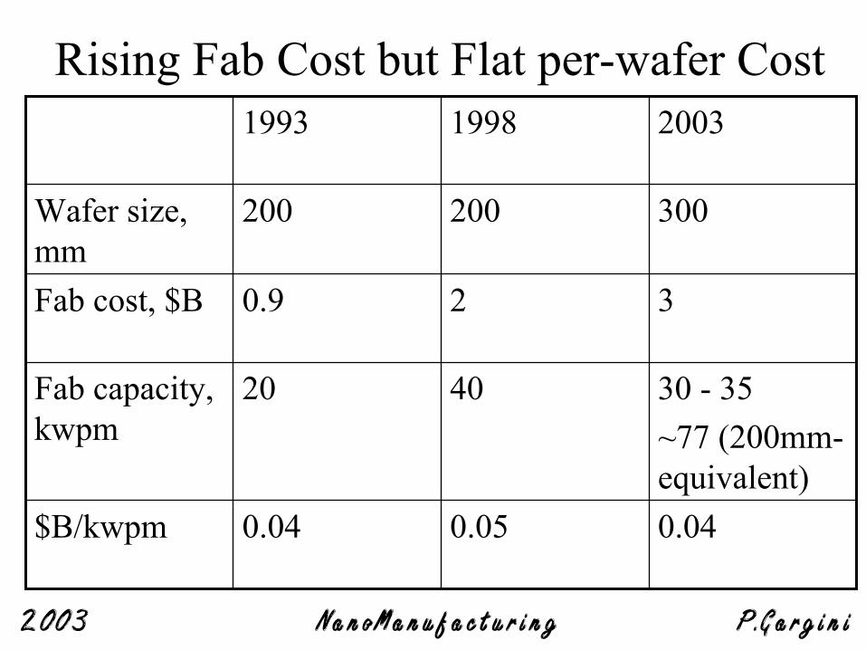
Rising Fab Cost but Flat per-wafer Cost
0.040.050.04$B/kwpm
30 - 35~77 (200mm-equivalent)
4020Fab capacity, kwpm
320.9Fab cost, $B
300200200Wafer size, mm
200319981993

NanoManufacturing2003 P.Gargini
Today’s Silicon Nanotechnology
• Technical wall at 100nm overtaken
• Economical wall at 300mm overtaken
• How far can silicon nanotechnology still go?

NanoManufacturing2003 P.Gargini
Simple Classification of Nanotechnology
1. The traditional evolution of the semiconductor industry (i.e., Quantum band gap and electron current)
• Germanium->Silicon->Carbon?
2. New devices enabled by semiconductor equipment plus new materials
• MEMS, NEMS, MRAM, FeRAM, OUM, Plastic Transistors etc.
3. Exploitation of additional Quantum properties• Spintronics, Quantum Computing, Teleportation etc.

NanoManufacturing2003 P.Gargini
Simple Classification of Nanotechnology
1. The traditional evolution of the semiconductor industry (i.e., Quantum band gap, tunneling and electron current)
• Germanium->Silicon->Carbon?
2. New devices enabled by semiconductor equipment plus new materials
• MEMS, NEMS, MRAM, FeRAM, OUM, Plastic Transistors etc.
3. Exploitation of additional Quantum properties• Spintronics, Quantum Computing, Teleportation etc.

NanoManufacturing2003 P.Gargini
The Ideal MOS Transistor
Fully SurroundingMetal Electrode
High-KGate Insulator
Fully Enclosed,DepletedSemiconductor
Band EngineeredSemiconductor
Low ResistanceSource/Drain
DrainSource
Metal Gate Insulator

NanoManufacturing2003 P.Gargini
90 nm Generation Transistor
50nm
Silicide Layer
Silicon Gate Electrode
1.2 nm SiO2Gate Oxide
Strained Silicon
2002IEDM, Source: Intel2002IEDM, Source: Intel

NanoManufacturing2003 P.Gargini
Gate Oxide Scaling
1
10
1990 1995 2000 2005
Gate Oxide Thickness
(nm)
1
10
1.2 nm
Thinner gate oxide increases transistor performanceThinner gate oxide increases transistor performance
90nm.13um
.18um
.25um
.35um
Generation

NanoManufacturing2003 P.Gargini
90 nm Generation Gate Oxide
1.2 nm SiO2
Gate oxide is less than 5 atomic layers thickGate oxide is less than 5 atomic layers thick
Polysilicon Gate Electrode
Silicon Substrate
SiliconSilicon
Nanotechnology Nanotechnology is here!is here!

NanoManufacturing2003 P.Gargini
Transistor Performance
Highest drive current in the industryHighest drive current in the industryReduced supply voltage for lower powerReduced supply voltage for lower power
0.0
0.2
0.4
0.6
0.8
1.0
1.2
1.4
1990 1995 2000 2005
Drive Current (mA/um)
1
10
Supply Voltage
(V)NMOS
PMOS
1.2V
90nm
.13um
.18um
.25um.35um
Generation

NanoManufacturing2003 P.Gargini
TunnelingBTB
E VB
E CB
EmissionThermionic
QMTunneling
DrainSourceLgate
Substrate
Gate
Source Drain
Gate Leakage
Channel Leakage
Electrostatic Scaling - Channel Leakage (Ioff)
Sum = Ioff
Channel Leakage

NanoManufacturing2003 P.Gargini
aw w
∆V
∆V
Eb
Eb
The field effect transistor (FET) can be thought of as consisting of two wells (source and drain) separated by a barrier (channel).
Figure 1. Energy Model for Limiting Devicew = width of Left-Hand Well (LHW) and Right-Hand Well (RHW)
a = barrier widthEb = barrier energy,

NanoManufacturing2003 P.Gargini
Minimum energy per switch operation as a function of minimum switch size
0
0.2
0.4
0.6
0.8
1
1.2
1.4
1.6
0 5 10 15 20
a, nm
E b/k
T numericalanalyticalkTln2