an instruction buffer for a low-power dsp 1 an instruction buffer for a low power dsp mike lewis...
Post on 20-Dec-2015
225 views
TRANSCRIPT
An instruction buffer for a low-power DSP 1
An Instruction Buffer for a Low Power DSP
Mike Lewis
AMULET group

An instruction buffer for a low-power DSP 2
A low-power DSP architecture
Targeted for digital mobile phones• Microprocessor + DSP combination
Multi-level power reduction strategy…• Asynchronous• Large register file• Parallel structure• Parallel instructions cached

An instruction buffer for a low-power DSP 3
A low-power DSP architecture
Fetch unit- autonomous instruction fetch
Register Bank (2x128x16 bit)
Load-store unit
ALU ALU ALU ALU
Index register values
Opcode
X/Y mem
P mem
int0, int1, nmi
Operand
Buffer
Decode
Index reg.
Fetch
VLIW mem
VLIW mem
VLIW mem
VLIW mem

An instruction buffer for a low-power DSP 4
A low-power DSP architecture
Instruction buffer: 32 entry FIFO
Register Bank (2x128x16 bit)
Load-store unit
ALU ALU ALU ALU
Index register values
Opcode
X/Y mem
P mem
int0, int1, nmi
Operand
Buffer
Decode
Index reg.
Fetch
VLIW mem
VLIW mem
VLIW mem
VLIW mem

An instruction buffer for a low-power DSP 5
A low-power DSP architecture
Decode instruction, read VLIW operand
Register Bank (2x128x16 bit)
Load-store unit
ALU ALU ALU ALU
Index register values
Opcode
X/Y mem
P mem
int0, int1, nmi
Operand
Buffer
Decode
Index reg.
Fetch
VLIW mem
VLIW mem
VLIW mem
VLIW mem

An instruction buffer for a low-power DSP 6
A low-power DSP architecture
Substitute and update index registers
Register Bank (2x128x16 bit)
Load-store unit
ALU ALU ALU ALU
Index register values
Opcode
X/Y mem
P mem
int0, int1, nmi
Operand
Buffer
Decode
Index reg.
Fetch
VLIW mem
VLIW mem
VLIW mem
VLIW mem
An instruction buffer for a low-power DSP 7
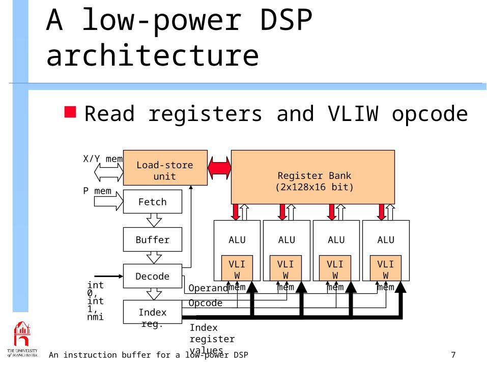
A low-power DSP architecture
Read registers and VLIW opcode
Register Bank (2x128x16 bit)
Load-store unit
ALU ALU ALU ALU
Index register values
Opcode
X/Y mem
P mem
int0, int1, nmi
Operand
Buffer
Decode
Index reg.
Fetch
VLIW mem
VLIW mem
VLIW mem
VLIW mem
An instruction buffer for a low-power DSP 8
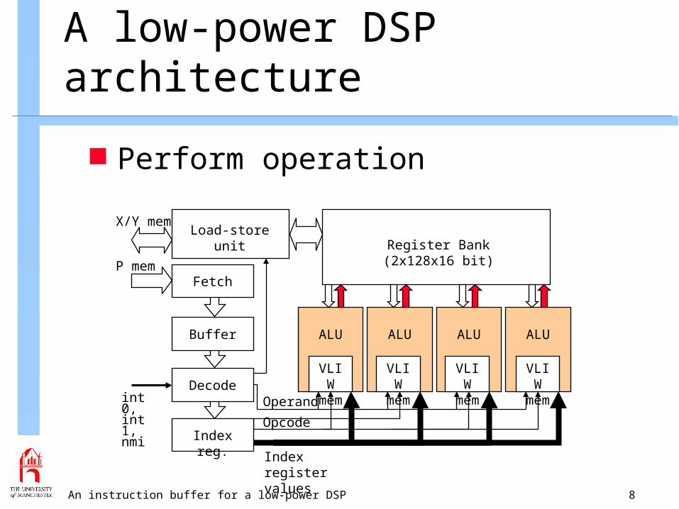
A low-power DSP architecture
Perform operation
Register Bank (2x128x16 bit)
Load-store unit
ALU ALU ALU ALU
Index register values
Opcode
X/Y mem
P mem
int0, int1, nmi
Operand
Buffer
Decode
Index reg.
Fetch
VLIW mem
VLIW mem
VLIW mem
VLIW mem
An instruction buffer for a low-power DSP 9
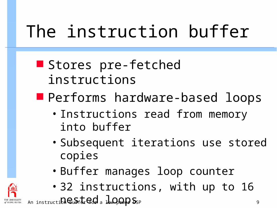
The instruction buffer
Stores pre-fetched instructions Performs hardware-based loops
• Instructions read from memory into buffer• Subsequent iterations use stored copies• Buffer manages loop counter• 32 instructions, with up to 16 nested loops
An instruction buffer for a low-power DSP 10
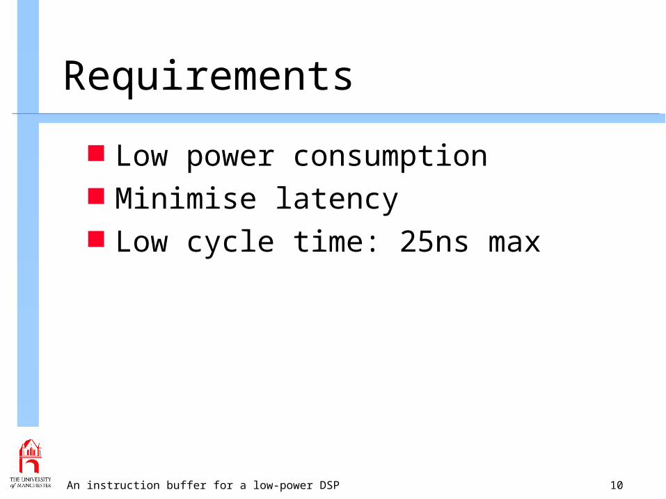
Requirements
Low power consumption Minimise latency Low cycle time: 25ns max
An instruction buffer for a low-power DSP 11
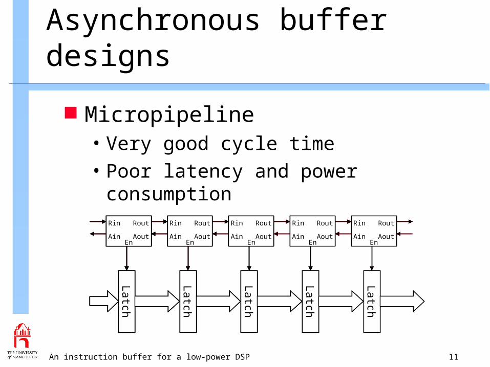
Asynchronous buffer designs
Micropipeline• Very good cycle time• Poor latency and power consumption
Latch
Ain
Rin
Aout
Rout
En
Latch
Ain
Rin
Aout
Rout
EnLatch
Ain
Rin
Aout
Rout
En
Latch
Ain
Rin
Aout
Rout
En
Latch
Ain
Rin
Aout
Rout
En
Latch
Ain
Rin
Aout
Rout
En
Latch
Ain
Rin
Aout
Rout
En
Latch
Ain
Rin
Aout
Rout
En
Latch
Ain
Rin
Aout
Rout
En
Latch
Ain
Rin
Aout
Rout
EnLatch
Ain
Rin
Aout
Rout
En
Latch
Ain
Rin
Aout
Rout
En
Latch
LatchAin
Rin
Aout
Rout
En
Latch
Ain
Rin
Aout
Rout
EnAin
Rin
Aout
Rout
En
Latch
Ain
Rin
Aout
Rout
En
Latch
Ain
Rin
Aout
Rout
En
Latch
Latch
Latch
Ain
Rin
Aout
Rout
EnAin
Rin
Aout
Rout
EnAin
Rin
Aout
Rout
En
Latch
Ain
Rin
Aout
Rout
En
Latch
Ain
Rin
Aout
Rout
En
Latch
Latch
Latch
Ain
Rin
Aout
Rout
EnAin
Rin
Aout
Rout
EnAin
Rin
Aout
Rout
EnAin
Rin
Aout
Rout
En
An instruction buffer for a low-power DSP 12
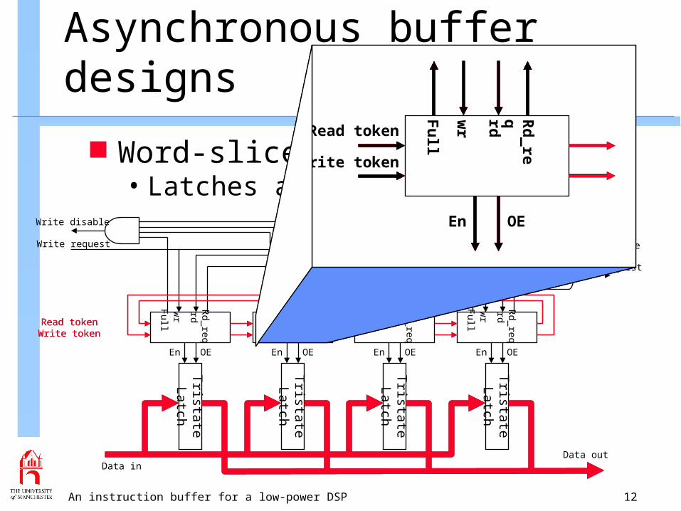
Asynchronous buffer designs
Word-slice FIFO• Latches arranged in parallel
Write tokenRead token
Tristate Latch
En OE
Fullwr rd Rd_req
Tristate Latch
En OE
Fullwr rd Rd_req
Tristate Latch
En OE
Fullwr rd Rd_req
Tristate Latch
En OE
Fullwr rd Rd_req
Write disable
Write request Read acknowledge
Read request
Data inData out
Write tokenRead token
En OE
Full
wr
rd Rd_req
Read token
Write token
En OE
Full
wr
rd Rd_req
Read token
Write token

An instruction buffer for a low-power DSP 13
Asynchronous buffer designs
• Writes disabled by ANDing full indications• Read requested by ORing all read requests
Write tokenRead token
Tristate Latch
En OE
Fullwr rd Rd_req
Tristate Latch
En OE
Fullwr rd Rd_req
Tristate Latch
En OE
Fullwr rd Rd_req
Tristate Latch
En OE
Fullwr rd Rd_req
Write disable
Write request Read acknowledge
Read request
Data inData out
An instruction buffer for a low-power DSP 15
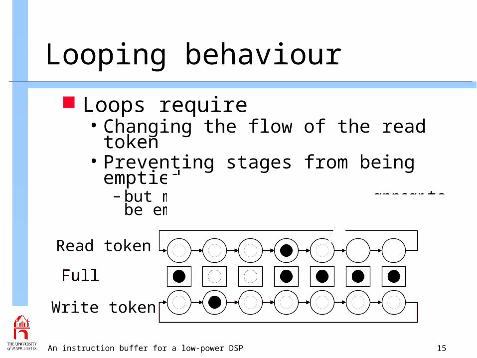
Looping behaviour
Loops require• Changing the flow of the read token• Preventing stages from being emptied
– but making sure that they appear to be empty
Read token
Write token
Loop start Loop end
FullFull
End of loopEnd of loop
Full

An instruction buffer for a low-power DSP 16
Evaluation
Power efficiency, latency, cycle-time• What defines ‘good’ performance?
Compare with a known design• 32-entry micropipeline FIFO chosen• Compare operation in non-looping mode

An instruction buffer for a low-power DSP 17
Evaluation
Powermill used to gather results• Test harness feeds identical random
instructions in both tests, at various speeds– and also ensures correct outputs
• Energy per transfer measured– at maximum throughput for each design– at a rate much less than the maximum

An instruction buffer for a low-power DSP 18
Results
Cycle time• 6.0ns (167MHz) for instruction buffer.• 2.0ns (488MHz) for micropipeline FIFO.
– The expected result: micropipeline FIFO is know to have good cycle time
• Instruction buffer well within 25ns target

An instruction buffer for a low-power DSP 19
Results
Latency• 2.7ns for instruction buffer• 26ns for micropipeline FIFO
– Big benefit from parallel structure
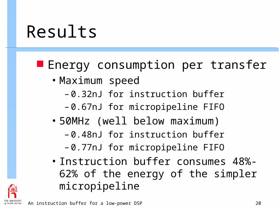
An instruction buffer for a low-power DSP 20
Results
Energy consumption per transfer• Maximum speed
– 0.32nJ for instruction buffer– 0.67nJ for micropipeline FIFO
• 50MHz (well below maximum)– 0.48nJ for instruction buffer– 0.77nJ for micropipeline FIFO
• Instruction buffer consumes 48%-62% of the energy of the simpler micropipeline

An instruction buffer for a low-power DSP 21
Conclusions
Cycle time well within specification Good latency achieved Low power consumption
• Outperforms much simpler FIFO design– Study on full extracted layout suggests word-
slice FIFO still better with wiring added [13]