an stm representation of the surface of silicon at the atomic level
TRANSCRIPT

An STM representation of the surface of silicon at the atomic level

What is Scanning Tunneling Microscopy?
Allows for the imaging of the surfaces of metals and semiconductors at the atomic level.
Developed by Gerd Binnig and Heinrich Rohrer at the IBM Zurich Research Laboratory in 1982.
The two shared half of the 1986 Nobel Prize in physics for developing STM.
Binnig Rohrer
STM has fathered a host of new atomic probe techniques: Atomic Force Microscopy, Scanning Tunneling Spectroscopy, Magnetic Force Microscopy, Scanning Acoustic Microscopy, etc.
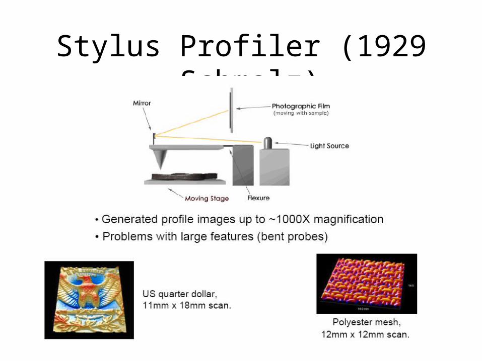
Stylus Profiler (1929 –Schmalz)
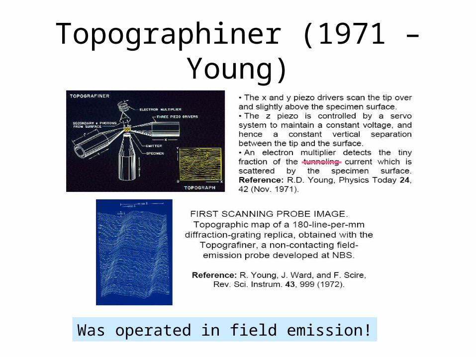
Topographiner (1971 –Young)
Was operated in field emission!

STM
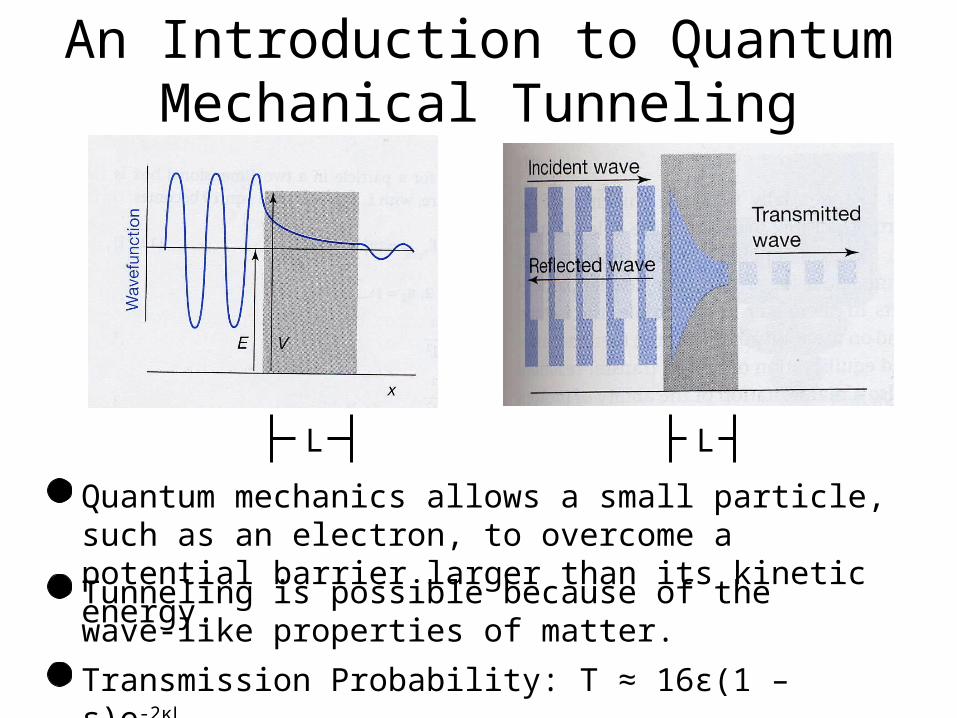
An Introduction to Quantum Mechanical Tunneling
Quantum mechanics allows a small particle, such as an electron, to overcome a potential barrier larger than its kinetic energy.
Tunneling is possible because of the wave-like properties of matter.
Transmission Probability: T ≈ 16ε(1 – ε)e-2κL
L L
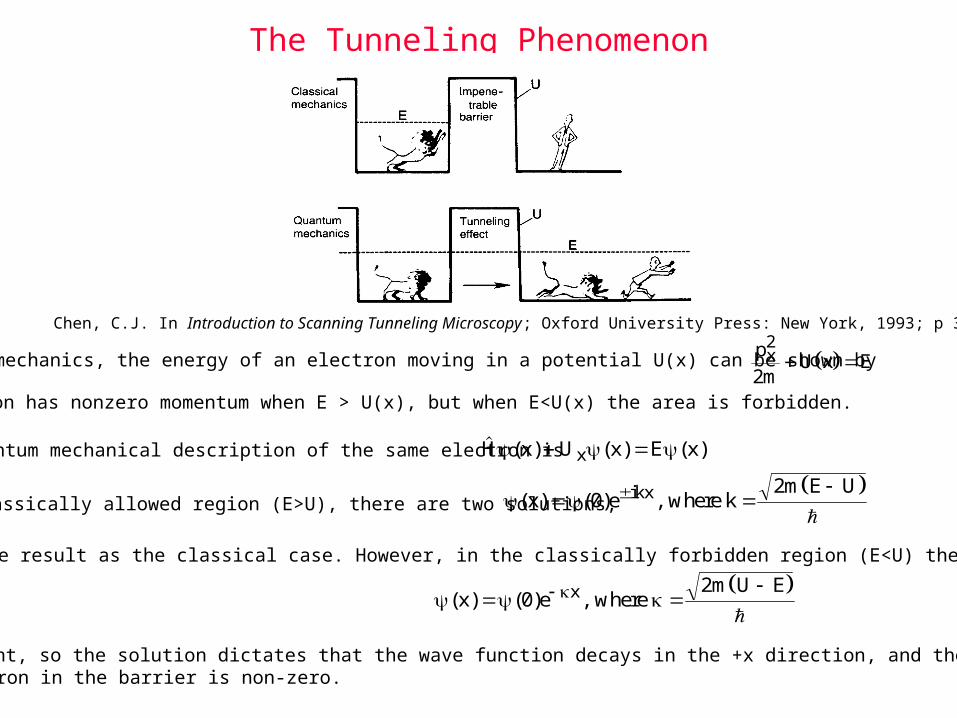
The Tunneling Phenomenon
In classical mechanics, the energy of an electron moving in a potential U(x) can be shown by p
mU x Ex
2
2
The electron has nonzero momentum when E > U(x), but when E<U(x) the area is forbidden.
The quantum mechanical description of the same electron is ( ) ( ) ( )H x U x E xx
In the classically allowed region (E>U), there are two solutions,
( ) ( ) ,x em E Uikx
02
where k
These give the same result as the classical case. However, in the classically forbidden region (E<U) the solution is
( ) ( ) ,x e
m U Ex 0
2 where
is a decay constant, so the solution dictates that the wave function decays in the +x direction, and the probability of finding an electron in the barrier is non-zero.
Chen, C.J. In Introduction to Scanning Tunneling Microscopy; Oxford University Press: New York, 1993; p 3.

Tunneling Energy Diagram
This diagram shows the bias dependence on tunneling. Ev is the vacuum level, or the referenceenergy level. EF is the Fermi level, which is the highest occupied level in a metal. s is the workfunction of the sample. The work function is defined as the amount of energy needed to remove an electron from the bulk to the vacuum level. The work function of the tip is labeled as t. If the sample bias is positive, the Fermi level of the sample is less than that of the tip, so electrons flow towards the sample. When the sample bias is negative, the Fermi level of the sample is at a higherlevel than that of the tip, so the electrons travel from the tip to the sample.
Behm, R.J.; Hosler, W. In Chemistry and Physics of Surfaces VI; Vanselow, R., Howe, R., Eds.; Springer: Berlin, 1986; p 361.

STM tips may (or may not) be complex
TipsCut platinum – iridium wires
Tungsten wire electrochemically etched
Tungsten sharpened with ion milling
Best tips have a point a few hundred nm wide
Vibration Control
Coiled spring suspension with magnetic damping
Stacked metal plates with dampers between them

Basic Principles of STM
Electrons tunnel between the tip and sample, a small current I is generated (10 pA to 1 nA).
I proportional to e-2κd, I decreases by a factor of 10 when d is increased by 1 Å.
d ~ 6 Å Bias voltage:mV – V range

Two Modes of Scanning
Constant Height Mode
Constant Current Mode
Usually, constant current mode is superior.

Instrumental Design: Controlling the Tip
Raster scanning
Precise tip control is achieved with Piezoelectrics
Displacement accurate to ± .05 Å

Interpreting STM Images
Hydrogen on Gadolinium
Scanning Tunneling Spectroscopy
“Topography” model good for large scale images, but not for the atomic level.
Electron charge density model more accurate for atomic level images.
Best model requires complex quantum mechanical considerations

Since you are measuring the electronic states, images of the same surface can vary!
First images were of the Si (111) reconstruction
The images vary depending on the electronic state of the material/tip.
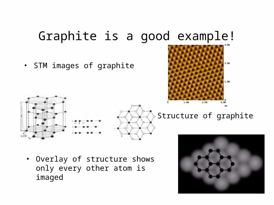
Graphite is a good example!
• STM images of graphite
Structure of graphite
• Overlay of structure shows only every other atom is imaged

Advantages
No damage to the sample
Vertical resolution superior to SEM
Spectroscopy of individual atoms
Relatively Low Cost
Disadvantages
Samples limited to conductors and semiconductors
Limited Biological Applications: AFM
Generally a difficult technique to perform
Figures of Merit
Maximum Field of View: 100 μm
Maximum Lateral Resolution: 1 Å
Maximum Vertical Resolution: .1 Å

Applications of STM
Stuff Physicists Do: Semiconductor surface structure, Nanotechnology, Superconductors, etc.
Surface Structure: Compare to bulk structure
Metal-catalyzed reactions
Spectroscopy of single atoms
Limited biological applications: Atomic Force Microscopy
Future Developments: Improve understanding of how electronic structure affects tunneling current, continue to develop STM offshoots

Interesting Images with STM
Copper Surface
Xenon on Nickel
Single atom lithography
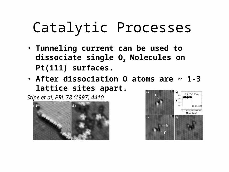
Catalytic Processes • Tunneling current can be used to dissociate single O2
Molecules on Pt(111) surfaces.
• After dissociation O atoms are ~ 1-3 lattice sites apart.Stipe et al, PRL 78 (1997) 4410.

Iron on Copper
Quantum Corrals
Imaging the standing wave created by interaction of species
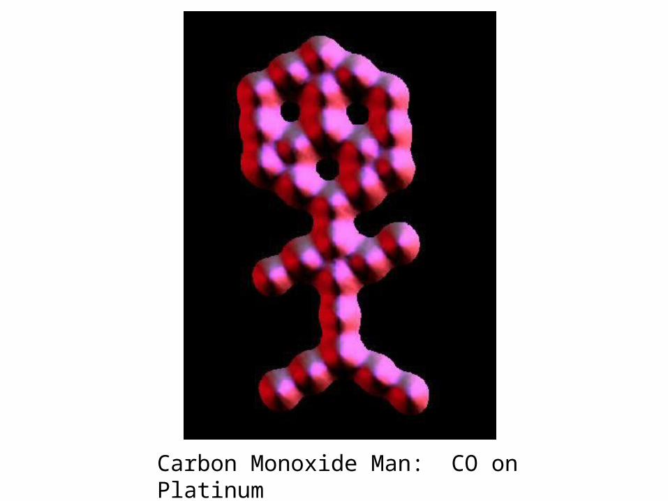
Carbon Monoxide Man: CO on Platinum

Question:
• At low voltages and temperature the tunneling current is given by:
• where d is the distance between the tip and sample, K is the decay constant, m is the mass of an electron, is the barrier height and ħ is planks constant. Assume the local barrier height is about 4eV. Show the current sensitivity to distance between the tip and sample if the current is kept within 2%.
mK
KdI
2
)2exp(

Answer
For
where
if current is kept to 2%, = 4eV, then
Very sensitive technique!
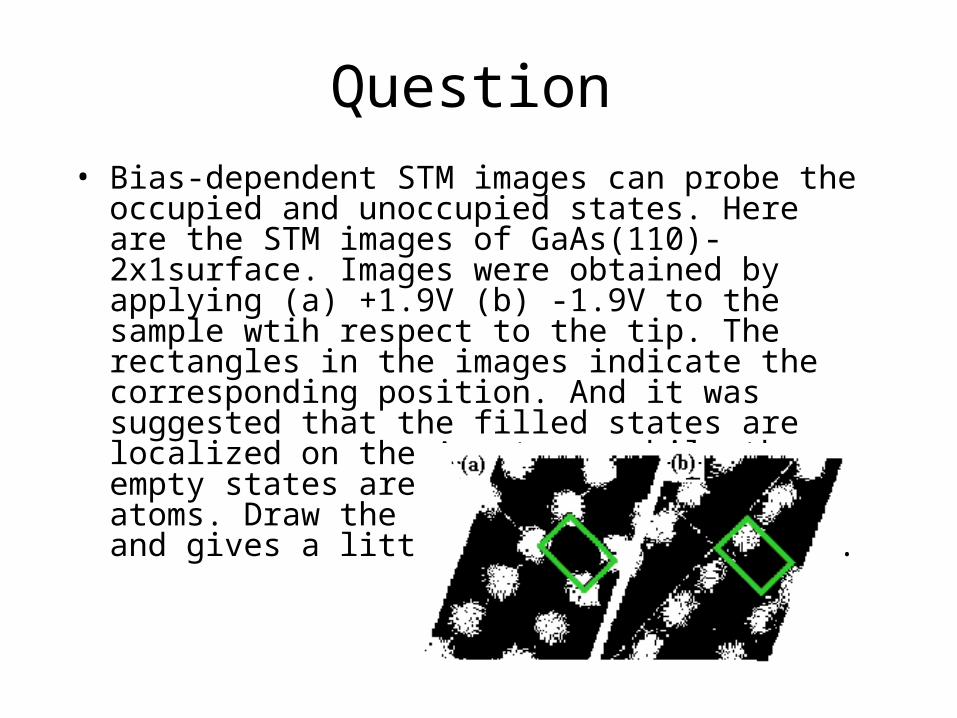
Question• Bias-dependent STM images can probe the occupied and
unoccupied states. Here are the STM images of GaAs(110)-2x1surface. Images were obtained by applying (a) +1.9V (b) -1.9V to the sample wtih respect to the tip. The rectangles in the images indicate the corresponding position. And it was suggested that the filled states are localized on the As atoms, while the empty states are localized on the Ga atoms. Draw the GaAs(110)-2x1 surface. and gives a little explanation as well.
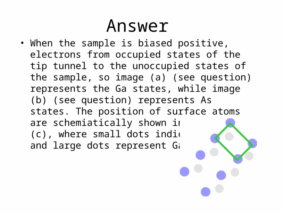
Answer• When the sample is biased positive, electrons from
occupied states of the tip tunnel to the unoccupied states of the sample, so image (a) (see question) represents the Ga states, while image (b) (see question) represents As states. The position of surface atoms are schemiatically shown in picture (c), where small dots indicate As atoms and large dots represent Ga atoms.
SourcesStroscio, Joseph A.; Kaiser, William J. Scanning Tunneling Microscopy. 1993. Academic Press, Inc. San Diego.
Golovchenko, JA. Science. 232, p. 48 – 53. Pool, Robert. Science. 247, p. 634 – 636.
Hansma, PK; Elings, VB; Marti, O; Bracker, CE. Science. 14 October 1988, p. 209 – 215.
STM Image Gallery. IBM Corporation 1995. http://www. almaden.ibm.com/vis/stm/gallery.html
“A Practical Guide to Scanning Probe Microscopy.” Veeco Metrology Group. http://www. topometrix.com/spmguide/contents.htm
Preuss, Paul. “A Close Look: Exploring the Mystery of the Surface.” Science Beat. April 12, 1999. http://www. lbl.gov/Science-Articles/Archive/STM-under-pressure.html
“Scanning Tunneling Microscopy.” National Center for Photovoltaics at the National Renewable Energy Laboratory. http://nrel.gov/measurements/tunnel.html
“Scanning Tunneling Microscopy.” http://www. physnet.uni-hamburg. de/home/vms/ pascal/stm.htm
“The Nobel Prize in Physics 1986.” Nobel e Museum. http://www. nobel.se/ physics/laureates/1986/index.html