an11037 ldo voltage regulators: fundamentals, topologies and parameters · 2016-04-26 · document...
TRANSCRIPT
AN11037LDO voltage regulators: fundamentals, topologies and parametersRev. 1 — 5 July 2013 Application note
Document information
Info Content
Keywords Low DropOut voltage regulator (LDO), efficiency, quiescent current, ground current, transient response, Equivalent Series Resistance (ESR), accuracy, load regulation, dropout voltage, delay circuit, standby current, line regulation, output noise, noise RMS, Power Supply Ripple Rejection (PSSR), start-up, soft start, inrush current, current limiter, foldback circuit, thermal shutdown, temperature watchdog
Abstract This application note illustrates the fundamentals of NXP LDO voltage regulators and explains their main parameters
NXP Semiconductors AN11037LDO voltage regulators: fundamentals, topologies and parameters
Revision history
Rev Date Description
1 20130705 Initial version
AN11037 All information provided in this document is subject to legal disclaimers. © NXP B.V. 2013. All rights reserved.
Application note Rev. 1 — 5 July 2013 2 of 25
Contact informationFor more information, please visit: http://www.nxp.com
For sales office addresses, please send an email to: [email protected]

NXP Semiconductors AN11037LDO voltage regulators: fundamentals, topologies and parameters
1. Introduction
A Low DropOut voltage regulator (LDO) reduces a DC input voltage to a specific DC output voltage. This application note illustrates the fundamentals and topologies of voltage regulators and explains their main parameters.
2. Fundamentals of low dropout voltage regulators
A typical LDO, as illustrated in Figure 1, includes pass element, resistors, overcurrent protection, voltage reference generator, thermal protection, feedback divider and error amplifier.
To simplify: An LDO (RLDO) and a load (RL) describe a setup of a resistor divider (see Figure 2, left side). The LDO behaves like an adjustable resistor (RLDO) which compensates the load change as well as source variations. The load (RL) is also described as adjustable because it can be a system with a dynamic power consumption. The target of an LDO is to keep the output voltage (VOUT) constant.
Fig 1. Schematic LDO
Fig 2. Simplified low dropout voltage regulator
THERMALPROTECTION
OVERCURRENTPROTECTION
VreferenceGENERATOR
VINVOUT
GND
R2
R1
VEN
RESR
CL(ext.) CL
VOUT
VIN
RL
RLDOVIN
VOUT
VIN
RL
VIN
Vref
AN11037 All information provided in this document is subject to legal disclaimers. © NXP B.V. 2013. All rights reserved.
Application note Rev. 1 — 5 July 2013 3 of 25

NXP Semiconductors AN11037LDO voltage regulators: fundamentals, topologies and parameters
The left schematic of Figure 2 describes the voltage divider which allows to calculate the output voltage of an LDO.
(1)
In order to keep the output voltage stable, RLDO has to change in function of RL. For an accurate output voltage, the output node must be control by itself. Therefore a pass element plus an error amplifier replace the RLDO.
A feedback path tracks the output voltage via a resistor divider. The signal is compared with a reference voltage, which is part of an LDO. The error amplifier adjusts the pass element (see Figure 2 right).
2.1 Difference between bipolar and MOS pass element
There are two kinds of pass elements for an LDO (Figure 3): a bipolar and a MOS transistor. Each architecture has an impact on dropout voltage, quiescent current, and the overall performance.
The bipolar transistor is current-driven by the base current which is proportional to the collector current. The MOS element is gate voltage driven. It means that most bipolar regulators have a higher ground current. Modern bipolar systems are often used for applications greater 5 V and for higher current ratings if ground current is negligible.
Voltage regulators with MOS pass elements allow a low voltage drop and can be optimized for ground current. For example, for mobile phones with a battery. Here the input voltage decreases after discharging the battery, nevertheless the output voltage has to be stable. MOS devices realize an on-resistance less than 0.1 and a dropout voltage less than 80 mV.
VOUT VIN RL RL RLDO+ =
Fig 3. Simplified low dropout voltage regulator
VIN
VOUT
CONTROLUNIT
GND VEN VIN
VOUT
CONTROLUNIT
GND VEN
AN11037 All information provided in this document is subject to legal disclaimers. © NXP B.V. 2013. All rights reserved.
Application note Rev. 1 — 5 July 2013 4 of 25

NXP Semiconductors AN11037LDO voltage regulators: fundamentals, topologies and parameters
3. Dropout Voltage
3.1 Description
The dropout voltage is the smallest input to output voltage difference at a specific current when the pass transistor works as a simple resistor.
For instance, an LDO has a PMOS pass element. The dropout voltage is equivalent to the drain-source voltage of the PMOS. The minimum dropout voltage of the LDO at a certain current is always limited by the PMOS / pass element output characteristic (see Figure 4).
If the input voltage of an LDO is higher than the output voltage, the error amplifier and gate driver force the gate of a pass transistor. As shown in Figure 4, the device operates in the saturation region. If the input voltage is near the nominal output voltage, the pass element works in the linear region. The pass element is limited by its on-resistance.
A small dropout voltage value guaranties possible lower power consumption and maximizes the efficiency.
Fig 4. Typical output characteristic of a PMOS
AN11037 All information provided in this document is subject to legal disclaimers. © NXP B.V. 2013. All rights reserved.
Application note Rev. 1 — 5 July 2013 5 of 25

NXP Semiconductors AN11037LDO voltage regulators: fundamentals, topologies and parameters
3.2 Data sheet values
In a data sheet, the dropout voltage is often described in two ways. The first one is only a value at a certain current (Table 1 operation point). The second one (Figure 5) is a characteristic of the dropout voltage in dependency of the output current for different temperatures.
Figure 6 can be used for both test setups. The dropout voltage over temperature describes the NXP LD6806 under the test conditions from Table 2.
Table 1. Dropout voltage LD6806CX4/25H
Symbol Parameter Conditions Min Typ Max Unit
Vdo dropout voltage IOUT = 200 mA; VIN > VO(nom)
- 60 100 mV
(1) Tamb = +85 C
(2) Tamb = +25 C
(3) Tamb = 40 C
Fig 5. Dropout voltage over temperature LD6806CX4/25H
Fig 6. Dropout voltage measurement circuit
IOUT (mA)0 20016080 12040
001aan787
40
60
20
80
100
Vdo(mV)
0
(1) (2) (3)
VIN VEN
Vdo
IOUT
COUT ROUTCIN
OUT
IN
001aan580
GND
ENDUT A
V
AN11037 All information provided in this document is subject to legal disclaimers. © NXP B.V. 2013. All rights reserved.
Application note Rev. 1 — 5 July 2013 6 of 25

NXP Semiconductors AN11037LDO voltage regulators: fundamentals, topologies and parameters
To use an LDO in a non-constant current mode, estimate the voltage dropout from Figure 5 or estimate the voltage drop as rude estimation:
(2)
4. Efficiency, quiescent current and standby current
4.1 Description
Quiescent or ground current, is the difference between input and output current. It describes the current which the LDO consumes by itself. A low quiescent current Iq improves the current efficiency of an LDO.
(3)
The quiescent current depends on the topology of an LDO. It is the sum of internal current sinks like, for example, band gap, error amplifier, resistor divider, pass element and drivers.
The LDO topologies from Figure 7 can theoretical have the same ground current when the load is 0 mA. When the load current increases, the MOS topology has a nearly linear increasing current consumption but the bipolar setup is not linear. The LDO with MOS device has only to drive the gate of MOS pass element. The main current depends on the resistor divider and the internal control logic.
As shown on the left side of Figure 7, an LDO with a bipolar pass element raises the quiescent current when the collector (load) current increases. This behavior is given by the base-current-driven pass element. Replacing the driver transistor against a
Table 2. LD6806: Dropout voltage test conditions
Symbol Parameter Conditions Min Typ Max Unit
VIN voltage on pin IN 0 - 5.5 V
VEN voltage on pin EN - 1.4 - V
CIN input capacitance case 0603 X5R - 1 - F
COUT output capacitance case 0603 X5R - 1 - F
IOUT current on pin OUT - 200 - mA
Dropout voltage Vdo typ IOUT load current=
Fig 7. Difference ground current caused by bipolar or MOS pass elements
Iq IIN IOUT–=
VOUT
VIN
RL
VIN
Vref
VOUT
VIN
RL
VIN
Vref
AN11037 All information provided in this document is subject to legal disclaimers. © NXP B.V. 2013. All rights reserved.
Application note Rev. 1 — 5 July 2013 7 of 25

NXP Semiconductors AN11037LDO voltage regulators: fundamentals, topologies and parameters
complementary driver transistor and implementing a current source would reduce the quiescent current. But in this case, the current consumption would be higher than for an equivalent MOS construction. The current consumption of both topologies is always a compromise of effort, cost and price.
The LDO efficiency is given by the equation:
(4)
Both topologies have a standby current which is the current consumption of the device under no-load, when the LDO is disabled.
4.1.1 Data sheet values
A comparison of LDOs quiescent current from different manufacturers is difficult. In order to compare LDOs with different topologies, NXP data sheets offer static values of quiescent current (see Table 3) and a chart of quiescent current versus load.
[1] Quiescent current is also called standby current or shut-down current.
Note: For devices with a battery, the quiescent current in Standby mode and under load is important. A lower quiescent current can increase charging cycles.
LDO efficiencyVOUT IOUT
VIN IOUT Iq+ ------------------------------------------ 100 %=
Table 3. Example for regulator quiescent current from LD6806CX4/25H data sheet
Symbol Parameter Conditions Min Typ Max Unit
Load regulation error
Iq quiescent current [1]
VEN = 1.4 V; IOUT = 0 mA - 70 100 A
VEN = 1.4 V; 0 mA < IOUT < 200 mA
- 155 250 A
VEN < 0.4 V - - 1 A
AN11037 All information provided in this document is subject to legal disclaimers. © NXP B.V. 2013. All rights reserved.
Application note Rev. 1 — 5 July 2013 8 of 25
NXP Semiconductors AN11037LDO voltage regulators: fundamentals, topologies and parameters
5. Output noise RMS (V)
5.1 Description
The output noise voltage of an LDO circuit is the intrinsic noise of an LDO. The internal noise sources are amplifiers, transistors, resistors, and so on. Supplied circuits like analog to digital converters, voltage references or digital circuits can influence the noise.
Nowadays there are only few LDO concepts using some special features to reduce the noise. The simplest concept is to filter the reference voltage (band gap) with an additional external capacitor. This construction creates a low pass and smooths the reference voltage of the LDO. Another concept is to reduce the bandwidth of the error amplifier, but it also reduces the transient response. It is a trade-off between noise performance and the step response of an LDO.
Linear regulator data sheets typically give two noise values:
• noise spectral density curve: V/√Hz as a function of frequency
• absolute result: V-RMS over a defined frequency range (typically 10 Hz to 100 kHz)
The absolute value is the integration of the noise spectral density curve over the bandwidth.
5.2 Data sheet values
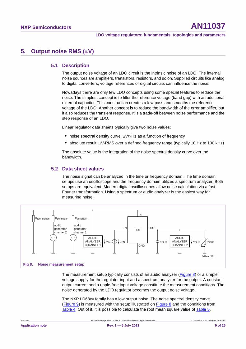
The noise signal can be analyzed in the time or frequency domain. The time domain setups use an oscilloscope and the frequency domain utilizes a spectrum analyzer. Both setups are equivalent. Modern digital oscilloscopes allow noise calculation via a fast Fourier transformation. Using a spectrum or audio analyzer is the easiest way for measuring noise.
The measurement setup typically consists of an audio analyzer (Figure 8) or a simple voltage supply for the regulator input and a spectrum analyzer for the output. A constant output current and a ripple-free input voltage constitute the measurement conditions. The noise generated by the LDO regulator becomes the output noise voltage.
The NXP LD68xy family has a low output noise. The noise spectral density curve (Figure 9) is measured with the setup illustrated on Figure 8 and the conditions from Table 4. Out of it, it is possible to calculate the root mean square value of Table 5.
Fig 8. Noise measurement setup
VIN VEN COUT ROUT
Rgenerator
OUT
IN
001aan581
GND
ENaudiogeneratorchannel 1
AUDIOANALYZERCHANNEL 1
DUT
Rgenerator
audiogeneratorchannel 2
Rtermination
VOUT
AUDIOANALYZERCHANNEL 2
AN11037 All information provided in this document is subject to legal disclaimers. © NXP B.V. 2013. All rights reserved.
Application note Rev. 1 — 5 July 2013 9 of 25

NXP Semiconductors AN11037LDO voltage regulators: fundamentals, topologies and parameters
Table 4. Test conditions for output noise test
Symbol Parameter Conditions Min Typ Max Unit
VIN voltage on pin IN 0 - 5.5 V
VEN voltage on pin EN - 1.4 - V
CIN input capacitance case 0603 X5R - 1 - F
COUT output capacitance case 0603 X5R - 1 - F
IOUT current on pin OUT - 200 - mA
Table 5. Example of output noise test conditions for output noise test
Symbol Parameter Conditions Min Typ Max Unit
Vn(o)RMS RMS output noise voltage
bandwidth 10 Hz to 100 kHz; COUT = 1 F
- 30 - V
(1) IOUT = 0 mA
(2) IOUT = 1 mA
(3) IOUT = 50 mA
(4) IOUT = 100 mA
(5) IOUT = 150 mA
(6) IOUT = 200 mA
Fig 9. Noise density test result for LD6806CX4/25H
001aan653
10−6
10−8
10−7
10−4
10−5
10−3
noise(VHz)
10−9
frequency (Hz)102 105104103
(4)(5)(6)
(1)(2)(3)
AN11037 All information provided in this document is subject to legal disclaimers. © NXP B.V. 2013. All rights reserved.
Application note Rev. 1 — 5 July 2013 10 of 25

NXP Semiconductors AN11037LDO voltage regulators: fundamentals, topologies and parameters
6. Power Supply Rejection Ratio (PSRR)
6.1 Description for PSRR
Power supply rejection ratio (PSRR) stands for the ratio of output noise to input noise at various frequencies. In other words, it is the capability of the regulator to suppress unwanted signals from the input to the output.
(5)
The PSRR is important for radio-frequency-sensitive applications. Noise or ripples of a supply, an improper PCB layout or a DC-to-DC converter which produces unwanted input voltage variations have to be filtered by an LDO.
There are two ways to measure PSRR. The first one is to use a digital oscilloscope and the second one is to use a network analyzer with two high impedance probes. The PSRR test setup (Figure 10) consists of a network analyzer which includes a pattern generator and high-ohmic probes, a preamplifier, a DC source and load. The pattern generator forces a sinus signal into a preamplifier and the output signal is mixed with a DC signal and forced into the LDO. The input and output voltage are measured with high impedance probes. The analyzer allows the deviation of the input and output voltage and describes the PSRR Figure 11.
As an advantage the network analyzer allow accurate measurements and can measure PSRR values greater than 100 dB. A state-of-the-art digital oscilloscope has a regulation down to millivolts allowing only a maximum PSRR measurement of about 65 dB. This measurement is not enough for high-performance LDOs in mobile application.
Fig 10. PSRR measurement circuit
PSRR (dB) 20V o ripple
V in ripple------------------------log=
VEN
Rprobe =1 MΩ
COUT ROUT VOUTCIN
OUT
IN
001aan582
GND
ENDUT
patterngeneratorRi = 50 Ω
NI-amplifiertest board
GVIN
Rprobe =1 MΩ
AN11037 All information provided in this document is subject to legal disclaimers. © NXP B.V. 2013. All rights reserved.
Application note Rev. 1 — 5 July 2013 11 of 25

NXP Semiconductors AN11037LDO voltage regulators: fundamentals, topologies and parameters
6.2 Data sheet values
Considering the PSRR values in data sheets of different manufacturers, it is difficult to establish an exact comparison. The output capacitor has a huge influence on the PSRR performance. For low voltage applications, an output capacitor of 1 F is often recommended. A bigger capacitance suppresses the output ripple and increases the PSRR value. Also an input voltage ripple has impact on the PSRR value. If the amplitude is reduced at the input, the PSRR value increases.
Today most LDOs have a proper PSRR performance in the lower frequency range but at high frequencies of about 1 MHz the PSRR decreases rapidly. PSRR is given by the topology of the LDO. More and more DC-to-DC converters increase the switching frequency from kHz to MHz. Digital circuits like microcontrollers create noise due to fast switching in the MHz range. For these reasons, there is more demand of LDOs with a better PSRR performance in the range above 1 MHz to protect sensitive Radio Frequency (RF) applications.
See Table 6 for typical test conditions for low voltage LDOs:
Table 6. LD68xy family: Test conditions for PSRR
Symbol Parameter Conditions Min Typ Max Unit
VIN voltage on pin IN 0 - 5.5 V
VEN voltage on pin EN - 1.4 - V
CIN input capacitance case 0603 X5R - 1 - F
COUT output capacitance case 0603 X5R - 1 - F
ROUT load on pin OUT - 13 -
IOUT current on pin OUT - 200 - mA
Fig 11. LD6835K/33H: Power supply rejection ratio
10 102 103 104 105 106 1070
22
44
66
88
110
frequency (Hz)
PSRRPSRRPSRR(dB)(dB)(dB)
IOUTOUT = 30 mA = 30 mAIOUT = 30 mAIOUTOUT = 300 mA = 300 mAIOUT = 300 mAIOUTOUT = 200 mA = 200 mAIOUT = 200 mAIOUTOUT = 100 mA = 100 mAIOUT = 100 mA
IOUTOUT = 50 mA = 50 mAIOUT = 50 mAIOUTOUT = 0 mA = 0 mAIOUT = 0 mA
IOUTOUT = 10 mA = 10 mAIOUT = 10 mAIOUTOUT = 1 mA = 1 mAIOUT = 1 mA
AN11037 All information provided in this document is subject to legal disclaimers. © NXP B.V. 2013. All rights reserved.
Application note Rev. 1 — 5 July 2013 12 of 25

NXP Semiconductors AN11037LDO voltage regulators: fundamentals, topologies and parameters
7. Start-up time, soft start, inrush current limiter and shut-down time
7.1 Description
Start-up time defines the time which the LDO needs for achieving 95 % of its typical output voltage level after activation via the enable pin.
For example, an LDO with a fast turn-on time and a heavy load can cause a voltage dip on the input. During the start-up time, the inrush current can exceed the maximum peak current of the LDO. This behavior depends on the capacitive and resistive load. In order to prevent peak current and massive voltage dips at the input for sensitive sources (for example, base bands in mobile phone), an inrush current limiter or soft-start circuit can be implemented into an LDO.
The soft start describes the dedicated start-up of integrated LDO elements (pass element, error amplifier and bang gap) step-by-step. This mode limits the inrush current to a certain level until the output voltage is raised. However the peak current depends on the load. An inherent inrush current limiter is used to limit inrush current and not to start softly. This limiter avoids excessive current when a power supply or the LDO is turned on independently from the load. It prevents damaging the connected circuits and eliminates voltage dips at the LDO input.
The shut-down time is the time which the LDO needs for reducing the output voltage to 10 % of the nominal output voltage after deactivating the enable pin. This parameter is massively influenced by the load capacitance as well as the load series resistance which is part of the discharge path. The test setup (Figure 12) can be used for all three parameters.
7.2 Data sheet values
In most data sheets, the values are measured under maximum load condition. When comparing data sheets, take notice that some manufacturers do not use only a capacitor at the output (Figure 12) but also a resistive load. Only a resistive load leads to less inrush current peaks, influences the comparability and does not represent the reality of a circuit.
Fig 12. Enable response measurement circuit (start-up, soft start and shut-down)
VIN VEN
Rint =1 MΩ
Rint =1 MΩ
COUT ROUT VOUTCINpatterngeneratorR = 50 Ω
OUT
IN
001aan300
GND
ENDUT
G
AN11037 All information provided in this document is subject to legal disclaimers. © NXP B.V. 2013. All rights reserved.
Application note Rev. 1 — 5 July 2013 13 of 25

NXP Semiconductors AN11037LDO voltage regulators: fundamentals, topologies and parameters
Table 7 shows the typical test conditions of start-up and shut-down time. Figure 13 and Figure 14 describe the test results measured with an oscilloscope.
Table 7. Test conditions for enable response test
Symbol Parameter Conditions Min Typ Max Unit
VIN voltage on pin IN 0 - 5.5 V
VEN voltage on pin EN - 1.4 - V
CIN input capacitance case 0603 X5R - 1 - F
COUT output capacitance case 0603 X5R - 1 - F
IOUT current on pin OUT - 200 - mA
Fig 13. Comparison start-up behavior of an LDO with and without soft start
time (ms)0 0.20.150.05 0.1
0.4
0.2
0.6
0.8
IOUT(A)
0
V(V)
1.0
3.0
2.0
4.0
0
Venable
VOUT (NO soft start)
VOUT soft start
IOUT (NO soft start)
IOUT (soft start)
AN11037 All information provided in this document is subject to legal disclaimers. © NXP B.V. 2013. All rights reserved.
Application note Rev. 1 — 5 July 2013 14 of 25

NXP Semiconductors AN11037LDO voltage regulators: fundamentals, topologies and parameters
8. Delay circuit only for dual LDO
8.1 Description
The delay circuit prevents an unwanted input voltage dip of a dual LDO when both outputs are enabled at the same time. The circuit delays the second LDO when enabling both LDOs simultaneously until the first LDO is ready.
8.2 Data sheet values
VIN = 5 V; CIN = 1 F; COUT = 1 F
(1) VEN
(2) VOUT
Fig 14. LD6806CX4/25H: Shut-down time
time (ms)0 0.40.30.20.1
001aan796
0.8
0.4
1.2
1.6
VEN(V)
0
1
2
3 VOUT(V)
0
(1) (2)
Fig 15. Delay circuit measurement setup
VIN VEN
COUT ROUT VOUT
CINpatterngeneratorR = 50 Ω OUT2
IN
GND
EN2DUT
G
EN1
COUT ROUT VOUT
OUT1
AN11037 All information provided in this document is subject to legal disclaimers. © NXP B.V. 2013. All rights reserved.
Application note Rev. 1 — 5 July 2013 15 of 25

NXP Semiconductors AN11037LDO voltage regulators: fundamentals, topologies and parameters
9. Line transient and line regulation response
9.1 Description
The line transient response is the maximum output voltage variation for an input voltage step change.
(6)
The line transient response can be caused by a disturbance, transient or a simple voltage change at the LDO input. The line response is often described in two ways. The first one is the static change, the second one the transient behavior. The static change is the delta between the output voltage at low input voltage and the output voltage at high input voltage. The transient behavior is the spike of the output voltage when the input voltage rises and falls from low to high and vice versa.
9.2 Data sheet values
Fig 16. Delay timing of a dual LDO with delay circuit
...
EN1, EN2
OUT1
tstartup(reg) tdelay
OUT2
Regulation % V VOUTVIN
----------------- 100VOUT-------------=
Fig 17. Line transient measurements setup
VEN
Rprobe =1 MΩ
COUT ROUT VOUTCIN
OUT
IN
001aan582
GND
ENDUT
patterngeneratorRi = 50 Ω
NI-amplifiertest board
GVIN
Rprobe =1 MΩ
AN11037 All information provided in this document is subject to legal disclaimers. © NXP B.V. 2013. All rights reserved.
Application note Rev. 1 — 5 July 2013 16 of 25

NXP Semiconductors AN11037LDO voltage regulators: fundamentals, topologies and parameters
For example, the test setup (Figure 17) and the test conditions of Table 8 allow switching the input voltage for an LD6806CX4/12H LDO from 2.1 V to 5.5 V. The graphic Figure 18 shows the input voltage and the resulting output voltage. The output voltage curve illustrates two peaks and a delta. The transient response is the maximum positive or negative peak of 7 mV and the delta is the line regulation and increasing from 1.2 V to 1.23 V.
Table 8. Test conditions for line transient test
Symbol Parameter Conditions Min Typ Max Unit
VIN voltage on pin IN 0 - 5.5 V
VEN voltage on pin EN - 1.4 - V
CIN input capacitance case 0603 X5R - 1 - F
COUT output capacitance case 0603 X5R - 1 - F
IOUT current on pin OUT - 200 - mA
Fig 18. Line transient (rising and falling edge) test result for LD6806CX4/12H
time (ms)0 0.80.60.2 0.4
001aan925
2
4
6
VIN(V)
0
1.4
1.8
1.2
1.6
2.0
VOUT(V)
1.0
(1)
(2)
AN11037 All information provided in this document is subject to legal disclaimers. © NXP B.V. 2013. All rights reserved.
Application note Rev. 1 — 5 July 2013 17 of 25
NXP Semiconductors AN11037LDO voltage regulators: fundamentals, topologies and parameters
10. Load transient response or load step response
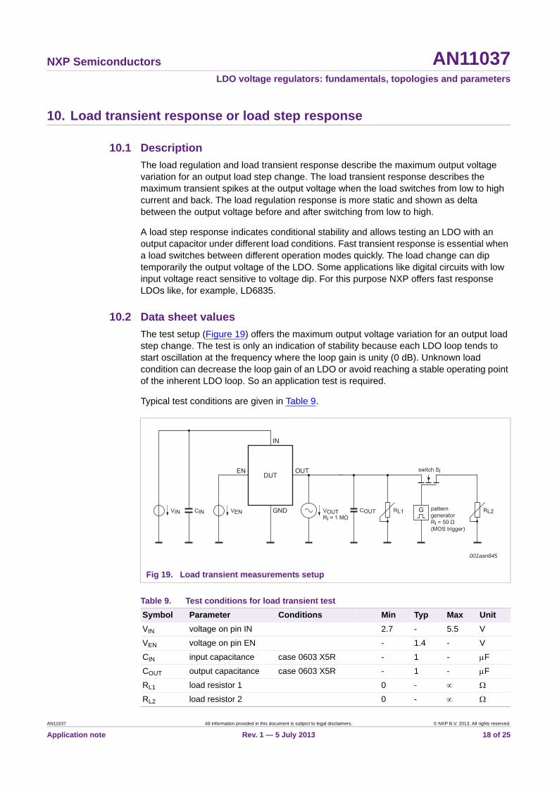
10.1 Description
The load regulation and load transient response describe the maximum output voltage variation for an output load step change. The load transient response describes the maximum transient spikes at the output voltage when the load switches from low to high current and back. The load regulation response is more static and shown as delta between the output voltage before and after switching from low to high.
A load step response indicates conditional stability and allows testing an LDO with an output capacitor under different load conditions. Fast transient response is essential when a load switches between different operation modes quickly. The load change can dip temporarily the output voltage of the LDO. Some applications like digital circuits with low input voltage react sensitive to voltage dip. For this purpose NXP offers fast response LDOs like, for example, LD6835.
10.2 Data sheet values
The test setup (Figure 19) offers the maximum output voltage variation for an output load step change. The test is only an indication of stability because each LDO loop tends to start oscillation at the frequency where the loop gain is unity (0 dB). Unknown load condition can decrease the loop gain of an LDO or avoid reaching a stable operating point of the inherent LDO loop. So an application test is required.
Typical test conditions are given in Table 9.
Fig 19. Load transient measurements setup
Table 9. Test conditions for load transient test
Symbol Parameter Conditions Min Typ Max Unit
VIN voltage on pin IN 2.7 - 5.5 V
VEN voltage on pin EN - 1.4 - V
CIN input capacitance case 0603 X5R - 1 - F
COUT output capacitance case 0603 X5R - 1 - F
RL1 load resistor 1 0 -
RL2 load resistor 2 0 -
VIN VOUTRi = 1 MΩ
VEN COUT RL2CIN
OUT
IN
GND
001aan845
ENDUT
RL1 patterngeneratorRi = 50 Ω(MOS trigger)
switch Si
G
AN11037 All information provided in this document is subject to legal disclaimers. © NXP B.V. 2013. All rights reserved.
Application note Rev. 1 — 5 July 2013 18 of 25

NXP Semiconductors AN11037LDO voltage regulators: fundamentals, topologies and parameters
Figure 20 shows the load transient response when the load of the LD6806Cx4/25H changes from 200 mA to 1 mA. The test analyses the dynamic behavior of the LDO and aim to detect unwanted conditions in combination with downstream circuits. One of the key benefits of the response test is its capability to detect the impact of output capacitor value to the output voltage variation. This capability is important for sensitive circuits which do not allow an input voltage variation more than 2 % to 10 %.
For example Figure 21 shows the impact of an output voltage variation when changing the capacitor with different ESR and ESL values. Each capacitor has an equivalent circuit and it is described by an ESR and an ESL value. The ESR value can reach from few milliohms up to several hundred milliohms. The time until the output voltage reaches its original value increases when the ESR value increases. For higher ESL values or inductive PCB parts, the voltage drop rises. Both impacts can cause an oscillation of an LDO, too.
(1) VOUT
(2) IOUT
Fig 20. Load transient (off) test result for LD6806CX4/25H
001aan800
time (ms)0 0.160.120.080.04
0.1
0.3
0.5
IOUT(A)
-0.1
2.4
2.5
VOUT(A)
2.3
(1) (2)
AN11037 All information provided in this document is subject to legal disclaimers. © NXP B.V. 2013. All rights reserved.
Application note Rev. 1 — 5 July 2013 19 of 25

NXP Semiconductors AN11037LDO voltage regulators: fundamentals, topologies and parameters
The best practice is to check the device under real load conditions and to check if the step response tends to oscillate. For NXP low voltage LDOs like LD6806, LD6805 or LD6815 the use of capacitors with a low ESR is the best choice. The devices should be placed as close as possible to the LDO.
11. Accuracy or output voltage variation
11.1 Description
The accuracy is the output voltage divergence of an LDO and is described over temperature.
This parameter is influenced by each part of the LDO. A semiconductor circuit (error amplifier, reference voltage, resistor divider (internal or external) or pass element) has a certain behavior over a specific temperature range and is influenced by the manufacturing process. The accuracy is the sum of all variations.
11.2 Data sheet values
The accuracy test setup is illustrated in Figure 22. The LDO is driven under different load and different temperature levels. For tests, the temperature changes from ambient in steps from low to high values and is controlled with a thermal control apparatus (thermo stream).
Fig 21. LD6806F/25H impact of output capacitor ESR and ESL to output voltage variation
time (ms)0 0.160.120.080.04
0.1
0.3
0.5
IOUT(A)
-0.1
2.40
2.50
VOUT(A)
2.30
increasing ESL
increasing ESR
2.35
2.45
2.55
AN11037 All information provided in this document is subject to legal disclaimers. © NXP B.V. 2013. All rights reserved.
Application note Rev. 1 — 5 July 2013 20 of 25

NXP Semiconductors AN11037LDO voltage regulators: fundamentals, topologies and parameters
Typical test conditions are: VIN = 2.2 V; COUT = 1 F and CIN = 1 F. As described in Figure 23, the accuracy, for example, for a LD6815TD is of about 3 % over temperature. The device is produced for low voltage applications in mobile devices.
Note: It is not possible to compare an accuracy of an LDO with and without inherent resistors. The accuracy of an adjustable LDO (without resistors) is always calculated without the tolerance of the inherent resistors divider for the feedback circuit.
Fig 22. Accuracy test setup
Fig 23. Accuracy LD6815TD/12x
AN11037 All information provided in this document is subject to legal disclaimers. © NXP B.V. 2013. All rights reserved.
Application note Rev. 1 — 5 July 2013 21 of 25

NXP Semiconductors AN11037LDO voltage regulators: fundamentals, topologies and parameters
12. Current limit, foldback circuit and thermal overload protection
12.1 Description
Current limiter and foldback circuits limit the current flow via an LDO when the device is used outside its specification. The current protection prevents device fail. This feature is required, for example, when the LDO output is accessible from the outside.
Example: An SD-card is tucked in an SD-card reader slot. A user breaks out the card from the slot with a screwdriver. During this procedure, it is possible to create a short between supply and ground. If it is not possible to disconnect the short, the device fails.
In this situation, an LDO with current protection shuts down and the device is not permanently damaged.
Therefore NXP includes three current protections in its low voltage LDOs.
The first one, a self-protection, is a thermal protection shutting down the device when a certain temperature on the LDO die is reached. The temperature watchdog helps avoiding overheating and short circuit. In order to prevent permanent damage, NXP LDOs with temperature watchdog can withstand short circuit until the watchdog is active.
The second protection is the current limiter (Figure 24 left). The feature is implemented in some LDOs for certain applications. The current limiter limits the current at a certain level until the current-demand declines.
The third protection is the foldback: a combination of a foldback circuit and a current limiter. A control unit observes the current flow. If the current overruns a certain level, the foldback circuit is activated and reduces the current to a defined level. A limiter clamps the current on a specific level. If the current decreases, the LDO switches off the limiter and starts up again. If the limit is reached again, the foldback is activated anew (Figure 24).
Fig 24. Current limiter and foldback
current foldback, then current limitercurrent limiter
CURRENTLIMITER
VOUT
IOUT
CURRENTFOLDBACK
VOUT
IOUT
CURRENTLIMITER
AN11037 All information provided in this document is subject to legal disclaimers. © NXP B.V. 2013. All rights reserved.
Application note Rev. 1 — 5 July 2013 22 of 25

NXP Semiconductors AN11037LDO voltage regulators: fundamentals, topologies and parameters
12.2 Data sheet values
Table 10 shows the static parameters from a data sheet. The thermal shutdown is typically at 160 C. When the junction temperature exceeds this value, the LDO shuts down. It restarts at normal operation when the temperature sinks below 140 C.
The short-circuit current describes two parameter arrangements. Without foldback, the short-circuit current is the value when the limiter starts operation. When a foldback circuit is implemented, the foldback current is the value when the foldback circuit starts operation. Then the short-circuit value is the current limit after foldback is activated.
13. Conclusion
This application note summarizes the most common test conditions for an LDO data sheet. It shows that a comparison of parameters from different manufacturers is not so easy. Each parameter follows special rules. The application note underlines that NXP Semiconductors has a standardized process to evaluate its LDO products, ensuring high quality for its customers.
Table 10. Data sheet values
Symbol Parameter Conditions Min Typ Max Unit
Tsd shutdown temperature - 160 - C
Tsd(hys) shutdown temperature hysteresis
- 20 - K
Isc short-circuit current VOUT = 0.0 V - 30 - mA
Ifold foldback current - 500 - mA
AN11037 All information provided in this document is subject to legal disclaimers. © NXP B.V. 2013. All rights reserved.
Application note Rev. 1 — 5 July 2013 23 of 25
NXP Semiconductors AN11037LDO voltage regulators: fundamentals, topologies and parameters
14. Legal information
14.1 Definitions
Draft — The document is a draft version only. The content is still under internal review and subject to formal approval, which may result in modifications or additions. NXP Semiconductors does not give any representations or warranties as to the accuracy or completeness of information included herein and shall have no liability for the consequences of use of such information.
14.2 Disclaimers
Limited warranty and liability — Information in this document is believed to be accurate and reliable. However, NXP Semiconductors does not give any representations or warranties, expressed or implied, as to the accuracy or completeness of such information and shall have no liability for the consequences of use of such information. NXP Semiconductors takes no responsibility for the content in this document if provided by an information source outside of NXP Semiconductors.
In no event shall NXP Semiconductors be liable for any indirect, incidental, punitive, special or consequential damages (including - without limitation - lost profits, lost savings, business interruption, costs related to the removal or replacement of any products or rework charges) whether or not such damages are based on tort (including negligence), warranty, breach of contract or any other legal theory.
Notwithstanding any damages that customer might incur for any reason whatsoever, NXP Semiconductors’ aggregate and cumulative liability towards customer for the products described herein shall be limited in accordance with the Terms and conditions of commercial sale of NXP Semiconductors.
Right to make changes — NXP Semiconductors reserves the right to make changes to information published in this document, including without limitation specifications and product descriptions, at any time and without notice. This document supersedes and replaces all information supplied prior to the publication hereof.
Suitability for use — NXP Semiconductors products are not designed, authorized or warranted to be suitable for use in life support, life-critical or safety-critical systems or equipment, nor in applications where failure or malfunction of an NXP Semiconductors product can reasonably be expected to result in personal injury, death or severe property or environmental damage. NXP Semiconductors and its suppliers accept no liability for inclusion and/or use of NXP Semiconductors products in such equipment or applications and therefore such inclusion and/or use is at the customer’s own risk.
Applications — Applications that are described herein for any of these products are for illustrative purposes only. NXP Semiconductors makes no representation or warranty that such applications will be suitable for the specified use without further testing or modification.
Customers are responsible for the design and operation of their applications and products using NXP Semiconductors products, and NXP Semiconductors accepts no liability for any assistance with applications or customer product design. It is customer’s sole responsibility to determine whether the NXP Semiconductors product is suitable and fit for the customer’s applications and products planned, as well as for the planned application and use of customer’s third party customer(s). Customers should provide appropriate design and operating safeguards to minimize the risks associated with their applications and products.
NXP Semiconductors does not accept any liability related to any default, damage, costs or problem which is based on any weakness or default in the customer’s applications or products, or the application or use by customer’s third party customer(s). Customer is responsible for doing all necessary testing for the customer’s applications and products using NXP Semiconductors products in order to avoid a default of the applications and the products or of the application or use by customer’s third party customer(s). NXP does not accept any liability in this respect.
Export control — This document as well as the item(s) described herein may be subject to export control regulations. Export might require a prior authorization from competent authorities.
Evaluation products — This product is provided on an “as is” and “with all faults” basis for evaluation purposes only. NXP Semiconductors, its affiliates and their suppliers expressly disclaim all warranties, whether express, implied or statutory, including but not limited to the implied warranties of non-infringement, merchantability and fitness for a particular purpose. The entire risk as to the quality, or arising out of the use or performance, of this product remains with customer.
In no event shall NXP Semiconductors, its affiliates or their suppliers be liable to customer for any special, indirect, consequential, punitive or incidental damages (including without limitation damages for loss of business, business interruption, loss of use, loss of data or information, and the like) arising out the use of or inability to use the product, whether or not based on tort (including negligence), strict liability, breach of contract, breach of warranty or any other theory, even if advised of the possibility of such damages.
Notwithstanding any damages that customer might incur for any reason whatsoever (including without limitation, all damages referenced above and all direct or general damages), the entire liability of NXP Semiconductors, its affiliates and their suppliers and customer’s exclusive remedy for all of the foregoing shall be limited to actual damages incurred by customer based on reasonable reliance up to the greater of the amount actually paid by customer for the product or five dollars (US$5.00). The foregoing limitations, exclusions and disclaimers shall apply to the maximum extent permitted by applicable law, even if any remedy fails of its essential purpose.
14.3 TrademarksNotice: All referenced brands, product names, service names and trademarks are the property of their respective owners.
AN11037 All information provided in this document is subject to legal disclaimers. © NXP B.V. 2013. All rights reserved.
Application note Rev. 1 — 5 July 2013 24 of 25

NXP Semiconductors AN11037LDO voltage regulators: fundamentals, topologies and parameters
15. Contents
1 Introduction . . . . . . . . . . . . . . . . . . . . . . . . . . . . 3
2 Fundamentals of low dropout voltage regulators . . . . . . . . . . . . . . . . . . . . . . . . . . . . . . 3
2.1 Difference between bipolar and MOS pass element . . . . . . . . . . . . . . . . . . . . . . . . . . . . . . . 4
3 Dropout Voltage . . . . . . . . . . . . . . . . . . . . . . . . . 53.1 Description . . . . . . . . . . . . . . . . . . . . . . . . . . . . 53.2 Data sheet values . . . . . . . . . . . . . . . . . . . . . . . 6
4 Efficiency, quiescent current and standby current . . . . . . . . . . . . . . . . . . . . . . . . . . . . . . . . 7
4.1 Description . . . . . . . . . . . . . . . . . . . . . . . . . . . . 74.1.1 Data sheet values . . . . . . . . . . . . . . . . . . . . . . . 8
5 Output noise RMS (mV). . . . . . . . . . . . . . . . . . . 95.1 Description . . . . . . . . . . . . . . . . . . . . . . . . . . . . 95.2 Data sheet values . . . . . . . . . . . . . . . . . . . . . . . 9
6 Power Supply Rejection Ratio (PSRR). . . . . . 116.1 Description for PSRR . . . . . . . . . . . . . . . . . . . 116.2 Data sheet values . . . . . . . . . . . . . . . . . . . . . . 12
7 Start-up time, soft start, inrush current limiter and shut-down time. . . . . . . . . . . . . . . . . . . . . 13
7.1 Description . . . . . . . . . . . . . . . . . . . . . . . . . . . 137.2 Data sheet values . . . . . . . . . . . . . . . . . . . . . . 13
8 Delay circuit only for dual LDO . . . . . . . . . . . 158.1 Description . . . . . . . . . . . . . . . . . . . . . . . . . . . 158.2 Data sheet values . . . . . . . . . . . . . . . . . . . . . . 15
9 Line transient and line regulation response . 169.1 Description . . . . . . . . . . . . . . . . . . . . . . . . . . . 169.2 Data sheet values . . . . . . . . . . . . . . . . . . . . . . 16
10 Load transient response or load step response. . . . . . . . . . . . . . . . . . . . . . . . . . . . . . 18
10.1 Description . . . . . . . . . . . . . . . . . . . . . . . . . . . 1810.2 Data sheet values . . . . . . . . . . . . . . . . . . . . . . 18
11 Accuracy or output voltage variation . . . . . . 2011.1 Description . . . . . . . . . . . . . . . . . . . . . . . . . . . 2011.2 Data sheet values . . . . . . . . . . . . . . . . . . . . . . 20
12 Current limit, foldback circuit and thermal overload protection . . . . . . . . . . . . . . . . . . . . . 22
12.1 Description . . . . . . . . . . . . . . . . . . . . . . . . . . . 2212.2 Data sheet values . . . . . . . . . . . . . . . . . . . . . . 23
13 Conclusion . . . . . . . . . . . . . . . . . . . . . . . . . . . . 23
14 Legal information. . . . . . . . . . . . . . . . . . . . . . . 2414.1 Definitions. . . . . . . . . . . . . . . . . . . . . . . . . . . . 2414.2 Disclaimers . . . . . . . . . . . . . . . . . . . . . . . . . . . 2414.3 Trademarks. . . . . . . . . . . . . . . . . . . . . . . . . . . 24
15 Contents. . . . . . . . . . . . . . . . . . . . . . . . . . . . . . 25
© NXP B.V. 2013. All rights reserved.
For more information, please visit: http://www.nxp.comFor sales office addresses, please send an email to: [email protected]
Date of release: 5 July 2013
Document identifier: AN11037
Please be aware that important notices concerning this document and the product(s)described herein, have been included in section ‘Legal information’.