an849 basic picmicro oscillator design
TRANSCRIPT
AN849Basic PICmicro® Oscillator Design
INTRODUCTION
The oscillator circuit for almost any microcontroller is afairly simple design with very few components. Select-ing the values for capacitors and resistors from themanufacturers’ data books will get you a circuit thatoscillates. However, many conditions can adverselyaffect the performance of your oscillator design. Highertemperatures and lower supply voltages can lower theamplifier gain (and thus the loop gain in the oscillatorcircuit) causing poor, slow, or no start-up. Colder tem-peratures and higher supply voltages can increaseamplifier gain, causing the circuit to be forced to ahigher harmonic and throw off the timing. The crystalcan also be overdriven and become potentially dam-aged and cease functioning altogether. It is also possi-ble to waste power through the improper selection ofcomponents or Clock modes.
The purpose of this Application Note is to provide a fun-damental explanation for the functioning of the oscilla-tor circuit, and to demonstrate some methods forassuring your design is sound. It is not intended tosupersede the data sheet in any way and is offered asdesign assistance to help the designer understand andverify their oscillator circuit. We will start with a discus-sion on the oscillator circuit itself, proceed to a descrip-tion of the function and characteristics of eachcomponent, offer several methods of improving andverifying your design, and conclude with a series of labexperiments which demonstrate the issues discussedhere. The goal is to help you achieve a fail-proof finaldesign that oscillates over the range of temperatureand voltage you expect your circuit to experience, with-out damaging components and leaving as much mar-gin for error as possible to overcome variations inboard manufacturing and silicon processes.
Most of the time using the values given in the manufac-turers’ data book tables will work fine. Microchip micro-controllers are able to run with clocks from 0.0 MHz toover 40 MHz, supply voltages from 2.0 VDC to 6.25 VDC
and temperatures from -40 degrees C to 125 degreesC, depending on the part and version ordered. All thismust be done with crystals or resonators of varyingquality and manufacture. This creates many chancesfor exceptions to the values given in the data book.
The Oscillator Circuit
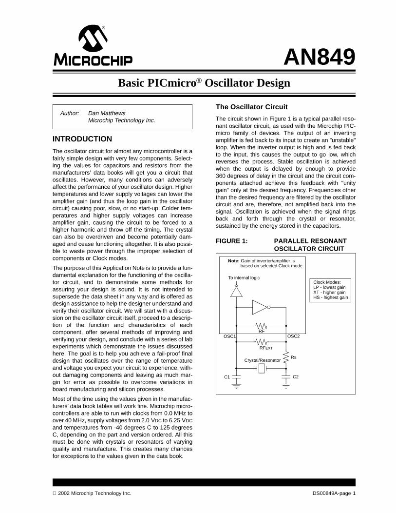
The circuit shown in Figure 1 is a typical parallel reso-nant oscillator circuit, as used with the Microchip PIC-micro family of devices. The output of an invertingamplifier is fed back to its input to create an "unstable"loop. When the inverter output is high and is fed backto the input, this causes the output to go low, whichreverses the process. Stable oscillation is achievedwhen the output is delayed by enough to provide360 degrees of delay in the circuit and the circuit com-ponents attached achieve this feedback with "unitygain" only at the desired frequency. Frequencies otherthan the desired frequency are filtered by the oscillatorcircuit and are, therefore, not amplified back into thesignal. Oscillation is achieved when the signal ringsback and forth through the crystal or resonator,sustained by the energy stored in the capacitors.
FIGURE 1: PARALLEL RESONANT OSCILLATOR CIRCUIT
Author: Dan MatthewsMicrochip Technology Inc.
Note: Gain of inverter/amplifier isbased on selected Clock mode
Crystal/ResonatorRS
C2C1
To internal logic
RFOSC1 OSC2
RFEXT
Clock Modes:LP - lowest gainXT - higher gainHS - highest gain
2002 Microchip Technology Inc. DS00849A-page 1

AN849
THE PURPOSE OF COMPONENTS AND CLOCK MODES
A good place to begin is with the purpose of each circuitcomponent. Because this is a loop circuit, a change inone component can change the effect of other compo-nents in the circuit. Therefore, a definition of purpose isa simplification for clarity only.
Inverting Amplifier
The Inverting Amplifier is the workhorse of the circuit. Itmust provide enough gain to amplify a very small signalat start-up where only noise is provided to the input.The desired signal is achieved only after the amplifiednoise has been filtered by the external oscillator circuitand fed back to the input, where it is further amplified.The amplifier amplifies all signals arbitrarily, so little fil-tering occurs there. Fortunately, crystals and resona-tors provide a band-pass function with very sharp cut-off. This helps assure that only the resonant crystal fre-quencies are permitted a path back to the amplifierinput, where they are added back into the signal tomake their way once more to the input, to be amplifiedyet again. If the desired signal is increased each timeuntil a stable oscillating signal is achieved, the circuit issaid to have Unity Gain at that frequency. In otherwords, there is enough gain for that signal to be sus-tained indefinitely. If the amplifier has much more gainthan necessary, then undesired noise still has a chanceof getting enough amplification to stay in the signal. Ifthere is not enough gain, then the desired signal is atrisk of being lost and the oscillator can die out or, morelikely, never start-up.
Because crystals and resonators have more than oneresonant frequency, part of the circuit designer’s job isto design the oscillator circuit such that undesired har-monics are not amplified enough to sustain oscillation.
Oscillation is achieved when a charge bounces backand forth through the crystal or resonator, between thecapacitors. The amplifier is then adding a push at theright time and of the right amount to sustain oscillation.This principal is very similar to the kind of push thatkeeps a pendulum swinging or a ball bouncing. If timedcorrectly (phase delay), and given the right amount ofenergy (gain), very little power is needed to sustain theoscillation. Therefore, the oscillator circuit can also bean important place to fine-tune performance to savepower. Crystals and resonators are so good at filteringfrequencies outside of the rated fundamental frequencythat the designer is mostly concerned with assuringthat:
• the desired frequency is sustained
• the circuit can start-up properly• energy is not wasted• noise is not unnecessarily amplified
Most of the discussion for this Application Note centerson understanding, achieving, and testing this idealdesign.
Clock Mode
The Clock mode is the programmable gain of theinverting amplifier (except RC or EC mode, which usesa RC network to determine oscillation frequency). Thelower Frequency modes have lower gain and the gainincreases for higher Frequency modes. For instance, inthe PIC16 family, the Clock mode gain from lowest tohighest is:
• LP (Low Power, or lowest gain)
• XT (standard Crystal mode, moderate gain)• HS (High Speed, or highest gain).
More energy is required to sustain higher frequencyoscillation and therefore, the higher Gain modes pro-vide the energy needed for higher speed operationwhile lower Gain modes reduce wasted power, over-drive and noise when running at lower frequencies.
The Microchip data book provides tables to guide in theselection of Clock modes. One such table is shown inTable 1.
TABLE 1: CAPACITOR SELECTION FOR CRYSTAL OSCILLATOR
Osc TypeCrystalFreq.
Cap. RangeC1
Cap. Range
C2
LP 32 kHz 33 pF 33 pF
200 kHz 15 pF 15 pF
XT 200 kHz 47-68 pF 47-68 pF
1 MHz 15 pF 15 pF
4 MHz 15 pF 15 pF
HS 4 MHz 15 pF 15 pF
8 MHz 15-33 pF 15-33 pF
20 MHz 15-33 pF 15-33 pF
Note: These values are for design guidance only.
Crystals Used
32 kHz Epson C-001R32.768K-A ±20 PPM
200 kHz STD XTL 200.000KHz ±20 PPM
1 MHz ECS ECS-10-13-1 ±50 PPM
4 MHz ECS ECS-40-20-1 ±50 PPM
8 MHz EPSON CA-301 8.000M-C ±30 PPM
20 MHz EPSON CA-301 20.000M-C ±30 PPM
DS00849A-page 2 2002 Microchip Technology Inc.
AN849
It is possible to select a higher or lower gain than spec-ified by the data book if desired, based on the specificneeds of the oscillator circuit. In circuits where lowpower consumption is critical, a lower gain Clock modecan help. Conversely, if the circuit is running at a lowvoltage or high temperatures, a higher gain may bedesirable. Unnecessarily overdriving crystals is to beavoided. There are potential trade-offs for selecting ahigher or lower Gain mode than needed. A higher Gainmode may improve start-up, but waste energy or over-drive a crystal. A lower Gain mode may save energyand reduce stress on the crystal, but fail to start-upunder certain conditions. (These topics are discussedin detail later).
The Crystal
The Crystal has its lowest AC impedance near the res-onant frequency. The crystal is placed in the pathbetween the output and input of the inverting amplifierto permit feedback and therefore oscillation at thedesired resonant frequency.
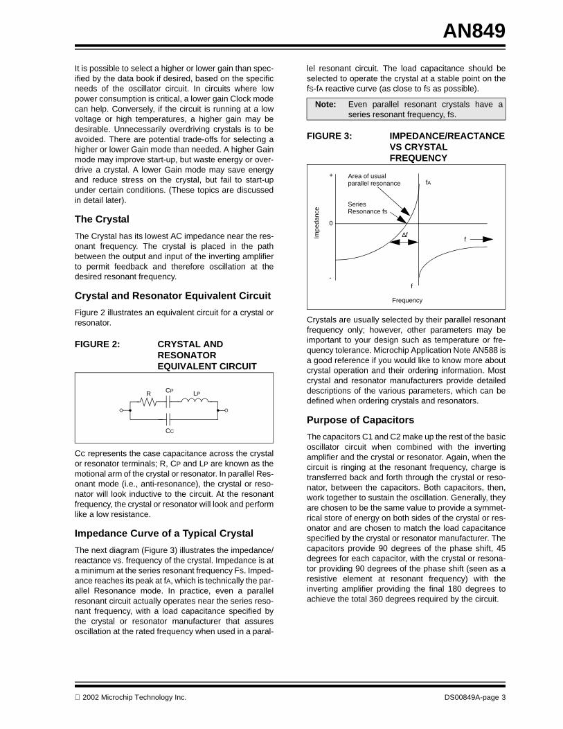
Crystal and Resonator Equivalent Circuit
Figure 2 illustrates an equivalent circuit for a crystal orresonator.
FIGURE 2: CRYSTAL AND RESONATOR EQUIVALENT CIRCUIT
CC represents the case capacitance across the crystalor resonator terminals; R, CP and LP are known as themotional arm of the crystal or resonator. In parallel Res-onant mode (i.e., anti-resonance), the crystal or reso-nator will look inductive to the circuit. At the resonantfrequency, the crystal or resonator will look and performlike a low resistance.
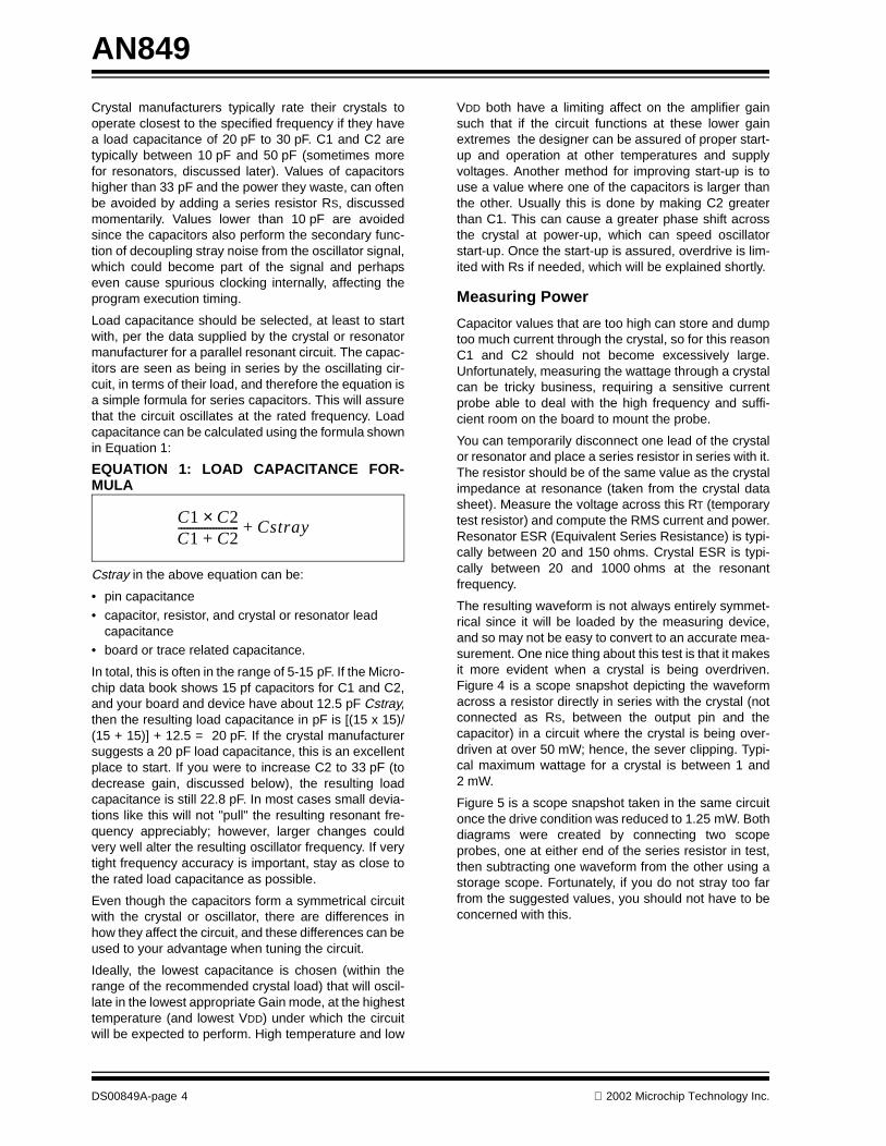
Impedance Curve of a Typical Crystal
The next diagram (Figure 3) illustrates the impedance/reactance vs. frequency of the crystal. Impedance is ata minimum at the series resonant frequency FS. Imped-ance reaches its peak at fA, which is technically the par-allel Resonance mode. In practice, even a parallelresonant circuit actually operates near the series reso-nant frequency, with a load capacitance specified bythe crystal or resonator manufacturer that assuresoscillation at the rated frequency when used in a paral-
lel resonant circuit. The load capacitance should beselected to operate the crystal at a stable point on thefS-fA reactive curve (as close to fS as possible).
FIGURE 3: IMPEDANCE/REACTANCE VS CRYSTAL FREQUENCY
Crystals are usually selected by their parallel resonantfrequency only; however, other parameters may beimportant to your design such as temperature or fre-quency tolerance. Microchip Application Note AN588 isa good reference if you would like to know more aboutcrystal operation and their ordering information. Mostcrystal and resonator manufacturers provide detaileddescriptions of the various parameters, which can bedefined when ordering crystals and resonators.
Purpose of Capacitors
The capacitors C1 and C2 make up the rest of the basicoscillator circuit when combined with the invertingamplifier and the crystal or resonator. Again, when thecircuit is ringing at the resonant frequency, charge istransferred back and forth through the crystal or reso-nator, between the capacitors. Both capacitors, then,work together to sustain the oscillation. Generally, theyare chosen to be the same value to provide a symmet-rical store of energy on both sides of the crystal or res-onator and are chosen to match the load capacitancespecified by the crystal or resonator manufacturer. Thecapacitors provide 90 degrees of the phase shift, 45degrees for each capacitor, with the crystal or resona-tor providing 90 degrees of the phase shift (seen as aresistive element at resonant frequency) with theinverting amplifier providing the final 180 degrees toachieve the total 360 degrees required by the circuit.
LPCP
CC
R
Note: Even parallel resonant crystals have aseries resonant frequency, fS.
Impe
danc
e
Area of usual
0
+
-f
fA
f∆f
parallel resonance
SeriesResonance fS
Frequency
2002 Microchip Technology Inc. DS00849A-page 3
AN849
Crystal manufacturers typically rate their crystals tooperate closest to the specified frequency if they havea load capacitance of 20 pF to 30 pF. C1 and C2 aretypically between 10 pF and 50 pF (sometimes morefor resonators, discussed later). Values of capacitorshigher than 33 pF and the power they waste, can oftenbe avoided by adding a series resistor RS, discussedmomentarily. Values lower than 10 pF are avoidedsince the capacitors also perform the secondary func-tion of decoupling stray noise from the oscillator signal,which could become part of the signal and perhapseven cause spurious clocking internally, affecting theprogram execution timing.
Load capacitance should be selected, at least to startwith, per the data supplied by the crystal or resonatormanufacturer for a parallel resonant circuit. The capac-itors are seen as being in series by the oscillating cir-cuit, in terms of their load, and therefore the equation isa simple formula for series capacitors. This will assurethat the circuit oscillates at the rated frequency. Loadcapacitance can be calculated using the formula shownin Equation 1:
EQUATION 1: LOAD CAPACITANCE FOR-MULA
Cstray in the above equation can be:
• pin capacitance
• capacitor, resistor, and crystal or resonator lead capacitance
• board or trace related capacitance.
In total, this is often in the range of 5-15 pF. If the Micro-chip data book shows 15 pf capacitors for C1 and C2,and your board and device have about 12.5 pF Cstray,then the resulting load capacitance in pF is [(15 x 15)/(15 + 15)] + 12.5 = 20 pF. If the crystal manufacturersuggests a 20 pF load capacitance, this is an excellentplace to start. If you were to increase C2 to 33 pF (todecrease gain, discussed below), the resulting loadcapacitance is still 22.8 pF. In most cases small devia-tions like this will not "pull" the resulting resonant fre-quency appreciably; however, larger changes couldvery well alter the resulting oscillator frequency. If verytight frequency accuracy is important, stay as close tothe rated load capacitance as possible.
Even though the capacitors form a symmetrical circuitwith the crystal or oscillator, there are differences inhow they affect the circuit, and these differences can beused to your advantage when tuning the circuit.
Ideally, the lowest capacitance is chosen (within therange of the recommended crystal load) that will oscil-late in the lowest appropriate Gain mode, at the highesttemperature (and lowest VDD) under which the circuitwill be expected to perform. High temperature and low
VDD both have a limiting affect on the amplifier gainsuch that if the circuit functions at these lower gainextremes the designer can be assured of proper start-up and operation at other temperatures and supplyvoltages. Another method for improving start-up is touse a value where one of the capacitors is larger thanthe other. Usually this is done by making C2 greaterthan C1. This can cause a greater phase shift acrossthe crystal at power-up, which can speed oscillatorstart-up. Once the start-up is assured, overdrive is lim-ited with Rs if needed, which will be explained shortly.
Measuring Power
Capacitor values that are too high can store and dumptoo much current through the crystal, so for this reasonC1 and C2 should not become excessively large.Unfortunately, measuring the wattage through a crystalcan be tricky business, requiring a sensitive currentprobe able to deal with the high frequency and suffi-cient room on the board to mount the probe.
You can temporarily disconnect one lead of the crystalor resonator and place a series resistor in series with it.The resistor should be of the same value as the crystalimpedance at resonance (taken from the crystal datasheet). Measure the voltage across this RT (temporarytest resistor) and compute the RMS current and power.Resonator ESR (Equivalent Series Resistance) is typi-cally between 20 and 150 ohms. Crystal ESR is typi-cally between 20 and 1000 ohms at the resonantfrequency.
The resulting waveform is not always entirely symmet-rical since it will be loaded by the measuring device,and so may not be easy to convert to an accurate mea-surement. One nice thing about this test is that it makesit more evident when a crystal is being overdriven.Figure 4 is a scope snapshot depicting the waveformacross a resistor directly in series with the crystal (notconnected as RS, between the output pin and thecapacitor) in a circuit where the crystal is being over-driven at over 50 mW; hence, the sever clipping. Typi-cal maximum wattage for a crystal is between 1 and2 mW.
Figure 5 is a scope snapshot taken in the same circuitonce the drive condition was reduced to 1.25 mW. Bothdiagrams were created by connecting two scopeprobes, one at either end of the series resistor in test,then subtracting one waveform from the other using astorage scope. Fortunately, if you do not stray too farfrom the suggested values, you should not have to beconcerned with this.
C1 C2×C1 C2+--------------------- Cstray+
DS00849A-page 4 2002 Microchip Technology Inc.
AN849
FIGURE 4: OVERDRIVEN CRYSTAL
FIGURE 5: NORMALLY DRIVEN CRYSTAL
Purpose of Resistors
RS is a series resistor that is selected to prevent over-driving the crystal. It is not often needed if gain (Clockmode), C1 and C2 are selected properly. If the circuit isbeing overdriven and a lower gain Clock mode cannotbe selected, then adding impedance with RS candecrease gain. This overdrive can be visually demon-strated by looking at the Osc-Out pin, which is thedriven pin, with an oscilloscope. Connecting the probeto the Osc-In pin will load the pin too much and nega-tively affect performance. The output signal should notbe clipped or squashed. Overdriving the crystal canalso lead to the circuit jumping to a higher harmonic.
RS is typically 40 K ohms or less, but is almost nevermore than 100 K ohms. If the value for RS is too high,then the high impedance input side of the amplifier maybe more susceptible to noise, very much the same waya pull-up resistor on an input pin is normally kept belowabout 50 K ohms to prevent noise from having enoughstrength to override the input.
Recall that the external circuit is supposed to provide180 degrees of loop delay. The amplifier provides180 degrees, or more. In some unusual cases, if theoutput from the amplifier is not delayed enough throughthe oscillator circuit to achieve its portion of the delaythen the oscillator may oscillate at a lower voltage. Thiscan be caused by high gain, which creates faster edgerates that reduce delay. Upon first inspection this canappear to be a paradox, because increased gain cansometimes result in reduced signal. In that case, it ispossible that increasing Rs will increase the phasedelay of the feedback circuit, bringing it in line withbeing 180 degrees out of phase between the amplifierinput and output, and oscillation voltage may actuallygo up, despite the expected decrease in gain. Think ofadding two sine waves together. If the waves are thesame frequency, the same amplitude and are in phase,then the result of adding the two signals together is asine wave of the same frequency with a gain of twicethe amplitude. If one of the input sine waves is shifted60 degrees from the other then the sum of the two willstill be the same frequency but the gain will now be con-siderably less than double the amplitude. (Try this in aspreadsheet if you would like to get a clearer picture).We will see this in one of the lab examples later on. Thefinal circuit must be evaluated throughly for these mar-ginal issues to ensure a robust design. Generally, thecrystal responds to its resonant frequency so well thatother components have minimal affect on the resultingfrequency.
RFEXT is selected to aid in start-up. RF (an internalFeedback FET) provides unfiltered feedback betweenthe output and input of the amplifier. Oscillators requiresome kind of "kick" to get them started ringing. Beforethe oscillation begins, noise must be amplified to causethe amplifier to begin generating a signal. Impedanceof RF is typically between 5 M ohms and 30 M ohmsfor IC-based oscillators tuned for crystals. Once oscil-lation at the resonant frequency is achieved, the imped-ance of the feedback circuit through the crystal is muchlower than the path provided through RF, and the noiseno longer affects oscillation. If more noise is needed toassist start-up (which is often the case for resonators)an external feedback resistor, RFEXT can be added.RFEXT is typically between 1 M ohms and 5 M ohms.
Again, RFEXT is most often needed for resonator cir-cuits. In almost every case where a problem with start-up occurred in a resonator-based oscillator circuit, add-ing RF of 1 M ohm solved the problem.
Note: Remember that a scope probe adds itsown capacitance to the circuit, so this mayhave to be accounted for in your design,(i.e., if circuit worked best with a C2 of20 pf and scope probe was 10 pf, a 30 pfcapacitor may actually be called for here).A J-fet input probe works nicely for mea-surements like this.
2002 Microchip Technology Inc. DS00849A-page 5
AN849
Overtones
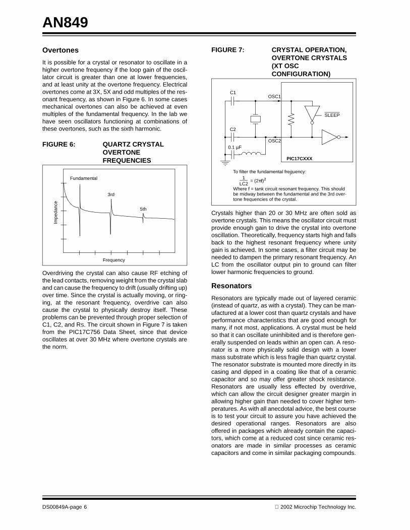
It is possible for a crystal or resonator to oscillate in ahigher overtone frequency if the loop gain of the oscil-lator circuit is greater than one at lower frequencies,and at least unity at the overtone frequency. Electricalovertones come at 3X, 5X and odd multiples of the res-onant frequency, as shown in Figure 6. In some casesmechanical overtones can also be achieved at evenmultiples of the fundamental frequency. In the lab wehave seen oscillators functioning at combinations ofthese overtones, such as the sixth harmonic.
FIGURE 6: QUARTZ CRYSTAL OVERTONE FREQUENCIES
Overdriving the crystal can also cause RF etching ofthe lead contacts, removing weight from the crystal slaband can cause the frequency to drift (usually drifting up)over time. Since the crystal is actually moving, or ring-ing, at the resonant frequency, overdrive can alsocause the crystal to physically destroy itself. Theseproblems can be prevented through proper selection ofC1, C2, and RS. The circuit shown in Figure 7 is takenfrom the PIC17C756 Data Sheet, since that deviceoscillates at over 30 MHz where overtone crystals arethe norm.
FIGURE 7: CRYSTAL OPERATION, OVERTONE CRYSTALS (XT OSC CONFIGURATION)
Crystals higher than 20 or 30 MHz are often sold asovertone crystals. This means the oscillator circuit mustprovide enough gain to drive the crystal into overtoneoscillation. Theoretically, frequency starts high and fallsback to the highest resonant frequency where unitygain is achieved. In some cases, a filter circuit may beneeded to dampen the primary resonant frequency. AnLC from the oscillator output pin to ground can filterlower harmonic frequencies to ground.
Resonators
Resonators are typically made out of layered ceramic(instead of quartz, as with a crystal). They can be man-ufactured at a lower cost than quartz crystals and haveperformance characteristics that are good enough formany, if not most, applications. A crystal must be heldso that it can oscillate uninhibited and is therefore gen-erally suspended on leads within an open can. A reso-nator is a more physically solid design with a lowermass substrate which is less fragile than quartz crystal.The resonator substrate is mounted more directly in itscasing and dipped in a coating like that of a ceramiccapacitor and so may offer greater shock resistance.Resonators are usually less effected by overdrive,which can allow the circuit designer greater margin inallowing higher gain than needed to cover higher tem-peratures. As with all anecdotal advice, the best courseis to test your circuit to assure you have achieved thedesired operational ranges. Resonators are alsooffered in packages which already contain the capaci-tors, which come at a reduced cost since ceramic res-onators are made in similar processes as ceramiccapacitors and come in similar packaging compounds.
Fundamental
3rd
5th
Frequency
Impe
danc
e
PIC17CXXX
C2
C1
0.1 µF
OSC1
SLEEP
OSC2
To filter the fundamental frequency:1
= (2πf)2LC2
Where f = tank circuit resonant frequency. This shouldbe midway between the fundamental and the 3rd over-tone frequencies of the crystal.
DS00849A-page 6 2002 Microchip Technology Inc.
AN849
Therefore, resonators can be manufactured withreduced overhead at a lower cost than a crystal andseparate capacitors. However, when it comes to meet-ing needs of outright accuracy, generally a crystal isselected.
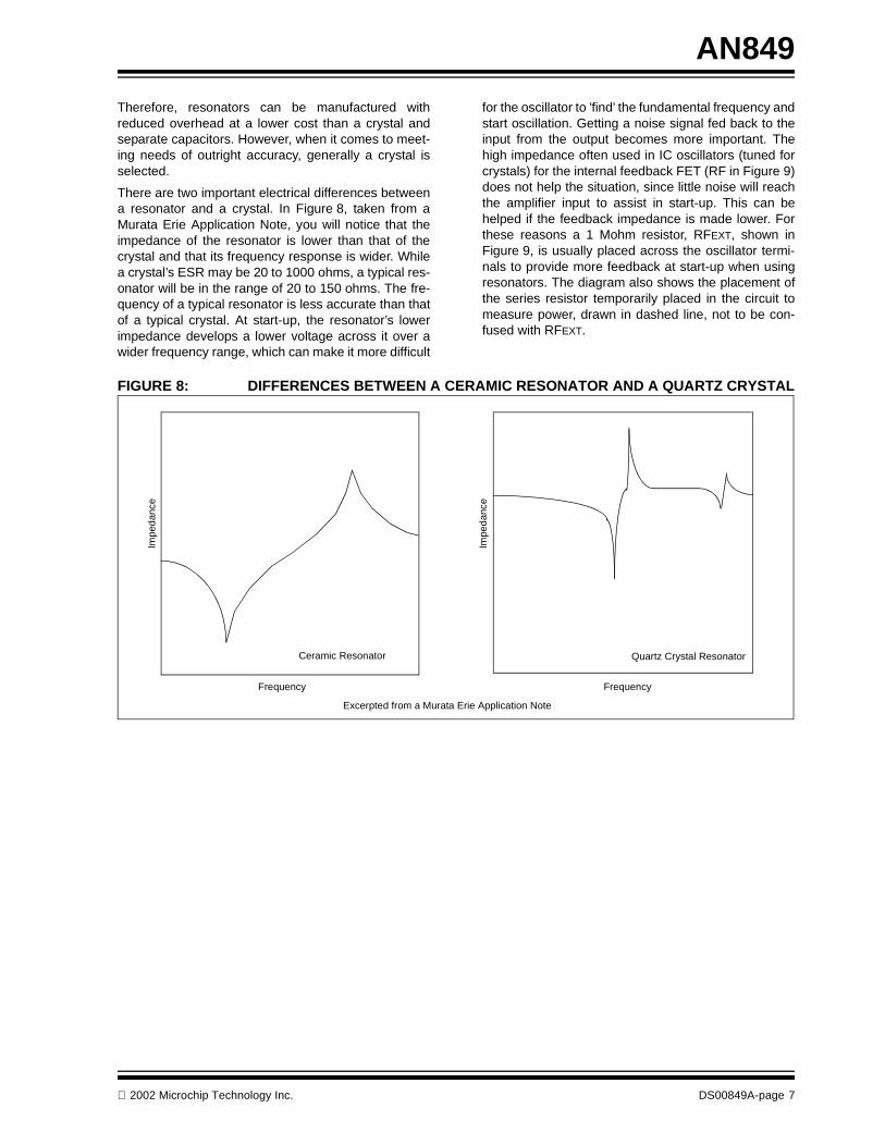
There are two important electrical differences betweena resonator and a crystal. In Figure 8, taken from aMurata Erie Application Note, you will notice that theimpedance of the resonator is lower than that of thecrystal and that its frequency response is wider. Whilea crystal’s ESR may be 20 to 1000 ohms, a typical res-onator will be in the range of 20 to 150 ohms. The fre-quency of a typical resonator is less accurate than thatof a typical crystal. At start-up, the resonator’s lowerimpedance develops a lower voltage across it over awider frequency range, which can make it more difficult
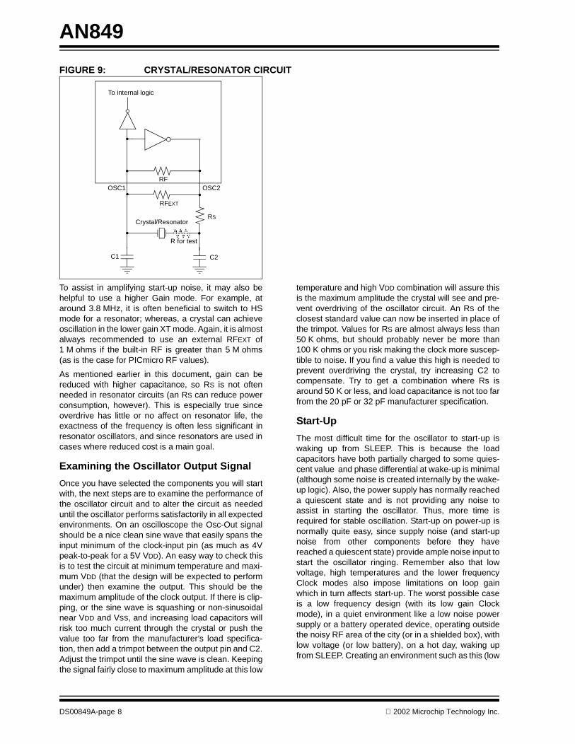
for the oscillator to ’find’ the fundamental frequency andstart oscillation. Getting a noise signal fed back to theinput from the output becomes more important. Thehigh impedance often used in IC oscillators (tuned forcrystals) for the internal feedback FET (RF in Figure 9)does not help the situation, since little noise will reachthe amplifier input to assist in start-up. This can behelped if the feedback impedance is made lower. Forthese reasons a 1 Mohm resistor, RFEXT, shown inFigure 9, is usually placed across the oscillator termi-nals to provide more feedback at start-up when usingresonators. The diagram also shows the placement ofthe series resistor temporarily placed in the circuit tomeasure power, drawn in dashed line, not to be con-fused with RFEXT.
FIGURE 8: DIFFERENCES BETWEEN A CERAMIC RESONATOR AND A QUARTZ CRYSTAL
Quartz Crystal ResonatorCeramic Resonator
Impe
danc
e
Impe
danc
e
Frequency Frequency
Excerpted from a Murata Erie Application Note
2002 Microchip Technology Inc. DS00849A-page 7
AN849
FIGURE 9: CRYSTAL/RESONATOR CIRCUIT
To assist in amplifying start-up noise, it may also behelpful to use a higher Gain mode. For example, ataround 3.8 MHz, it is often beneficial to switch to HSmode for a resonator; whereas, a crystal can achieveoscillation in the lower gain XT mode. Again, it is almostalways recommended to use an external RFEXT of1 M ohms if the built-in RF is greater than 5 M ohms(as is the case for PICmicro RF values).
As mentioned earlier in this document, gain can bereduced with higher capacitance, so RS is not oftenneeded in resonator circuits (an RS can reduce powerconsumption, however). This is especially true sinceoverdrive has little or no affect on resonator life, theexactness of the frequency is often less significant inresonator oscillators, and since resonators are used incases where reduced cost is a main goal.
Examining the Oscillator Output Signal
Once you have selected the components you will startwith, the next steps are to examine the performance ofthe oscillator circuit and to alter the circuit as neededuntil the oscillator performs satisfactorily in all expectedenvironments. On an oscilloscope the Osc-Out signalshould be a nice clean sine wave that easily spans theinput minimum of the clock-input pin (as much as 4Vpeak-to-peak for a 5V VDD). An easy way to check thisis to test the circuit at minimum temperature and maxi-mum VDD (that the design will be expected to performunder) then examine the output. This should be themaximum amplitude of the clock output. If there is clip-ping, or the sine wave is squashing or non-sinusoidalnear VDD and VSS, and increasing load capacitors willrisk too much current through the crystal or push thevalue too far from the manufacturer’s load specifica-tion, then add a trimpot between the output pin and C2.Adjust the trimpot until the sine wave is clean. Keepingthe signal fairly close to maximum amplitude at this low
temperature and high VDD combination will assure thisis the maximum amplitude the crystal will see and pre-vent overdriving of the oscillator circuit. An RS of theclosest standard value can now be inserted in place ofthe trimpot. Values for RS are almost always less than50 K ohms, but should probably never be more than100 K ohms or you risk making the clock more suscep-tible to noise. If you find a value this high is needed toprevent overdriving the crystal, try increasing C2 tocompensate. Try to get a combination where Rs isaround 50 K or less, and load capacitance is not too farfrom the 20 pF or 32 pF manufacturer specification.
Start-Up
The most difficult time for the oscillator to start-up iswaking up from SLEEP. This is because the loadcapacitors have both partially charged to some quies-cent value and phase differential at wake-up is minimal(although some noise is created internally by the wake-up logic). Also, the power supply has normally reacheda quiescent state and is not providing any noise toassist in starting the oscillator. Thus, more time isrequired for stable oscillation. Start-up on power-up isnormally quite easy, since supply noise (and start-upnoise from other components before they havereached a quiescent state) provide ample noise input tostart the oscillator ringing. Remember also that lowvoltage, high temperatures and the lower frequencyClock modes also impose limitations on loop gainwhich in turn affects start-up. The worst possible caseis a low frequency design (with its low gain Clockmode), in a quiet environment like a low noise powersupply or a battery operated device, operating outsidethe noisy RF area of the city (or in a shielded box), withlow voltage (or low battery), on a hot day, waking upfrom SLEEP. Creating an environment such as this (low
To internal logic
RFOSC1 OSC2
Crystal/Resonator
RFEXT
R for test
C1 C2
RS
DS00849A-page 8 2002 Microchip Technology Inc.
AN849
voltage, high temp, shielded, wake-up from SLEEP) isa good test to see if your circuit has good start-up char-acteristics.
As mentioned previously, a number of things can bedone to assist start-up. These include:
• A 1M to 5M ohm resistor placed across the oscil-lator terminals to provide more feedback at start-up (RFEXT in Figure 9).
• Selecting a higher Gain mode, to increase amplifi-cation of noise at start-up.
• Unbalancing the capacitors by making one a higher capacitance than the other (usually C2 is made higher than C1).
Higher gain causes more noise to be fed back into thesignal and creates a faster start-up edge that can helpreduce start-up time. C2 may have to be increased ordecreased and/or an RS added to prevent overdrivingthe crystal.
In the very rare cases where your circuit is alreadyexpected to operate in an exceptionally quiet environ-ment (i.e., with voltage at the minimum and tempera-ture fairly high) you may have to provide some start-upnoise yourself. Otherwise, there is not much margin leftto test to and assure a fail-proof design. There is an olddesigner's tip that a cheap RS or RFEXT resistor, suchas a carbon film or carbon composition resistor, canactually help start oscillation. All resistance generatessome amount of noise which, when placed in the crys-tal oscillator path or on the input, can assist start-up. Ifyou have a button that will be pressed, or some signalto wake up the part, then a capacitor from that signal tothe oscillator input can provide the start-up jolt that isneeded. This should be a wake-up signal and not a sig-nal that would be generating noise while the circuit isrunning; otherwise, another technique to eliminate thesignal when it was not needed would have to beemployed. It is also possible to connect the oscillatorcircuit grounds to VDD instead, with the benefit of theusual additional noise that is introduced by a VDD refer-ence. This is typically not done, but can be beneficial incertain situations such as this.
It is also possible for a circuit with too much gain to notstart-up. This usually happens most often at low fre-quencies, like 32 kHz, since at high frequencies thehigh gain is dissipated more easily by the load capaci-tance.
Other Design Considerations
The actual board design is not covered here in muchdetail since that subject can become lengthy on its own.Consider studying the related subjects of high-speeddesign and analog design techniques as well as han-dling noise and ESD. However, a few tips are worthmentioning:
1. Keep the oscillator circuit trace lengths to a min-imum and away from signals that can injectunwanted noise, or may be affected by the sig-nal of the oscillator.
2. Where an oscillator or timer input pin is next toanother active output pin, consider routing oneof the signals away from the chip and the othertowards the underside of the chip, so that theyare adjacent only at the pins themselves and thetraces are never adjacent.
3. Avoid sharp angles in the traces, which cancause reflections. (Though this is sometimesdisputed).
4. Board manufacturing and assembly techniquescan also affect oscillator performance. Forinstance, there have been several occasionswhere the oscillator failed to start and the failurewas traced back to contamination on the board.Contaminants on surface mount boards areespecially a problem, as contaminants becometrapped under a surface mount crystal or reso-nator. If the contaminant is at all conductive, orcan ionize in humidity (such as a salt-basedboard wash), then a second feedback pathbetween the oscillator input and output is cre-ated which can prevent start-up or affect the run-ning oscillator performance.
The Final Test
With all of the parameters and conditions that must belooked after and the shortage of all the data necessaryfor a reliable mathematical model for an oscillator, itmay seem quite difficult to design an oscillator circuitthat can be assured to run in a wide range of environ-ments. The good news is that if you find the ideal"sweet spot" for the oscillator you can overcome tem-perature, voltage and part-to-part drift. If you have amarginal design and do not know it these factors cancause the circuit to malfunction unexpectedly. If youidentify the margins for the environment that your cir-cuit will run in and verify its performance, within orbeyond those margins, you should find that the oscilla-tor performs as desired over a very wide range ofchanges. The most important point is to be aware ofwhere these marginal areas exist, then verify that yourdesign works correctly in all cases. Once that is donethere is very little left to worry about. We suggest thatdesigners test their circuits under the worst possibleconditions. In fact it is possible to exceed the operatingspecification of the part, for purposes of these tests,perhaps while holding it in RESET to prevent improperexecution from causing power consumption problems.
The following tests are suggested:
• Start by selecting C1 and C2 per the Microchip data book.
• Test at maximum VDD and Lowest temperature.• Test at minimum VDD and Highest temperature
2002 Microchip Technology Inc. DS00849A-page 9
AN849
• Test for wake-up from SLEEP with high tempera-ture, low voltage and quiet DC supply.
• Adjust C1, C2 and RS as needed and repeat tests until satisfactory results are achieved
Check that the output sine wave is not clipping in thehighest gain environment of highest VDD and lowesttemperature. Also, make sure that the sine outputamplitude is great enough in the lowest gain environ-ment of lowest VDD (and highest temperature) to coverthe logic input requirements of the clock. A value of 4Vpeak-to-peak is usually fine, but refer to the data sheetfor the final specification requirements. Then, at thehighest temperature, with the lowest VDD the circuit willhave to run at, running from a quiet battery if possible,in as quiet an environment (RF and electrically speak-ing) as your board will see, test the part to make sure itwakes up from SLEEP. If all this checks out and yourcapacitance values are low enough, (and within rangeto prevent unnecessary power consumption) then youshould have a clean, trouble-free oscillator design.
A Note on External Clocks
If the PICmicro oscillator is not being used and thedevice will be driven from an external clock, be sure toset the Clock mode to something other than RC mode,since this mode will fight with the injected input. Ideally,you would select the mode that corresponds to the fre-quency injected, but this is of less importance heresince the clock is only driving its internal logic and nota crystal loop circuit. It may be possible to select aClock mode lower than would be needed by an oscilla-tor circuit, and thereby save some of the power thatwould be used exercising the inverting amplifier.
A Demonstration of Oscillator Circuit Performance Problems.
A number of tests were conducted in the lab to demon-strate the various problems encountered with marginaloscillator designs. Start-up, overdrive, under-drive, har-monics and ideal characteristics were all evaluated andthe results captured on an oscilloscope. In this series oftests, the start-up performances of a number of circuitswere tested. The test circuit setup was as follows:
Test Circuit Setup
• A fixed DC supply and a switch created VDD ramp up. To assure equivalent comparisons, anything without a consistent power-up ramp was rejected.
• Code was written to initialize ports and start tog-gling RB0 immediately to illustrate code start-up time.
• The Oscillator output pin, Osc 2 or Osc Out, was measured and displayed against the other sig-nals, VDD and RB0 (toggling with code execution).
• The PICmicro enters SLEEP mode upon press of an input switch. WDT is disabled, so wake-up from SLEEP only occurs on MCLR Reset.
This test circuit assures a consistent power-up ramp sothat start-up can be measured with the same referencepoint. All signal images were captured from an oscillo-scope. If there is an apparent difference in the VDD
start-up ramp, it is solely because of the time-base set-tings of the scope setup. It should also be noted that, inmany cases, the captured oscillator sine wave is notnecessarily drawn accurately compared to the oscilla-tor frequency as there are some display harmonicsdepending on the screen refresh rate and resolution.Counting cycles will not be an accurate measurementof apparent frequency. This is specifically where thescope refresh rate is slowed to very low speeds toobserve oscillator ring-up. Where the signal is beingexamined for its frequency content, the signal was iso-lated at a rate compatible with accurate screen display.In many cases, capacitors, Gain mode and otherparameters were forced out of specification to demon-strate the ill effects of an improperly designed circuit.Where improper performance is pointed out, the designcould easily be remedied with the advice already givenabove.
DS00849A-page 10 2002 Microchip Technology Inc.
AN849
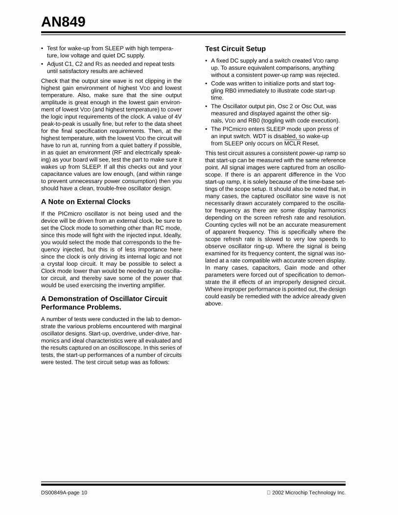
Baseline Comparison - RC Mode
The fastest possible start-up is the RC or EC Oscillatormodes (see Figure 10). Here we see the oscillatorstarts up immediately with the power-up ramp. Codeexecution also begins immediately since there is no1024 start-up count for RC mode.
FIGURE 10: BASELINE COMPARISON - RC MODE
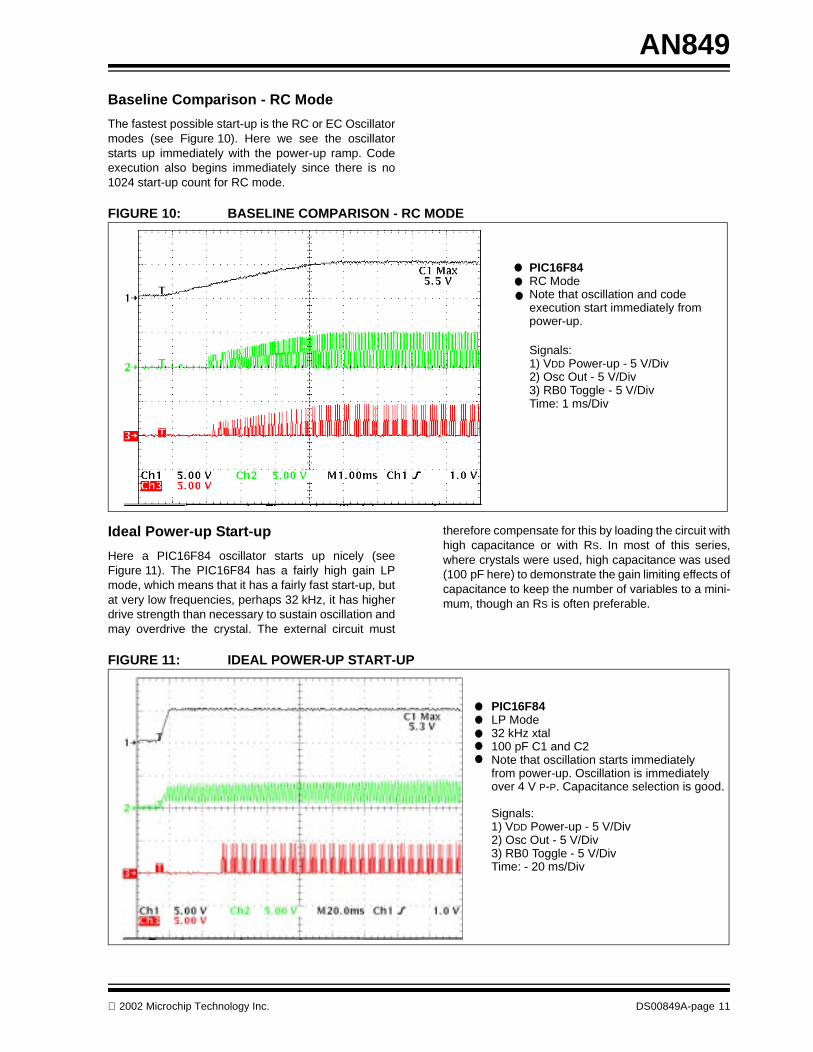
Ideal Power-up Start-up
Here a PIC16F84 oscillator starts up nicely (seeFigure 11). The PIC16F84 has a fairly high gain LPmode, which means that it has a fairly fast start-up, butat very low frequencies, perhaps 32 kHz, it has higherdrive strength than necessary to sustain oscillation andmay overdrive the crystal. The external circuit must
therefore compensate for this by loading the circuit withhigh capacitance or with RS. In most of this series,where crystals were used, high capacitance was used(100 pF here) to demonstrate the gain limiting effects ofcapacitance to keep the number of variables to a mini-mum, though an RS is often preferable.
FIGURE 11: IDEAL POWER-UP START-UP
Signals:1) VDD Power-up - 5 V/Div2) Osc Out - 5 V/Div3) RB0 Toggle - 5 V/DivTime: 1 ms/Div
PIC16F84RC ModeNote that oscillation and codeexecution start immediately frompower-up.
PIC16F84LP Mode32 kHz xtal100 pF C1 and C2Note that oscillation starts immediatelyfrom power-up. Oscillation is immediatelyover 4 V P-P. Capacitance selection is good.
Signals:1) VDD Power-up - 5 V/Div2) Osc Out - 5 V/Div3) RB0 Toggle - 5 V/DivTime: - 20 ms/Div
2002 Microchip Technology Inc. DS00849A-page 11
AN849
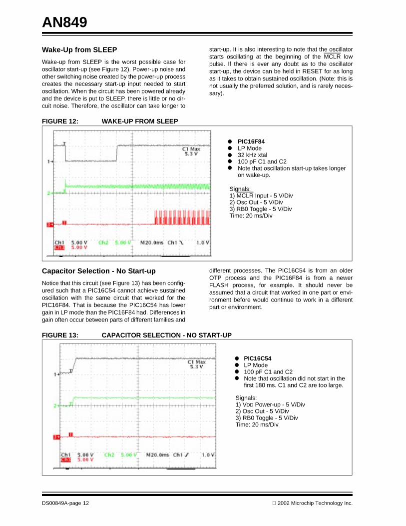
Wake-Up from SLEEP
Wake-up from SLEEP is the worst possible case foroscillator start-up (see Figure 12). Power-up noise andother switching noise created by the power-up processcreates the necessary start-up input needed to startoscillation. When the circuit has been powered alreadyand the device is put to SLEEP, there is little or no cir-cuit noise. Therefore, the oscillator can take longer to
start-up. It is also interesting to note that the oscillatorstarts oscillating at the beginning of the MCLR lowpulse. If there is ever any doubt as to the oscillatorstart-up, the device can be held in RESET for as longas it takes to obtain sustained oscillation. (Note: this isnot usually the preferred solution, and is rarely neces-sary).
FIGURE 12: WAKE-UP FROM SLEEP
Capacitor Selection - No Start-up
Notice that this circuit (see Figure 13) has been config-ured such that a PIC16C54 cannot achieve sustainedoscillation with the same circuit that worked for thePIC16F84. That is because the PIC16C54 has lowergain in LP mode than the PIC16F84 had. Differences ingain often occur between parts of different families and
different processes. The PIC16C54 is from an olderOTP process and the PIC16F84 is from a newerFLASH process, for example. It should never beassumed that a circuit that worked in one part or envi-ronment before would continue to work in a differentpart or environment.
FIGURE 13: CAPACITOR SELECTION - NO START-UP
PIC16F84LP Mode32 kHz xtal100 pF C1 and C2Note that oscillation start-up takes longeron wake-up.
Signals: 1) MCLR Input - 5 V/Div2) Osc Out - 5 V/Div3) RB0 Toggle - 5 V/DivTime: 20 ms/Div
PIC16C54LP Mode100 pF C1 and C2Note that oscillation did not start in thefirst 180 ms. C1 and C2 are too large.
Signals:1) VDD Power-up - 5 V/Div2) Osc Out - 5 V/Div3) RB0 Toggle - 5 V/DivTime: 20 ms/Div
DS00849A-page 12 2002 Microchip Technology Inc.
AN849
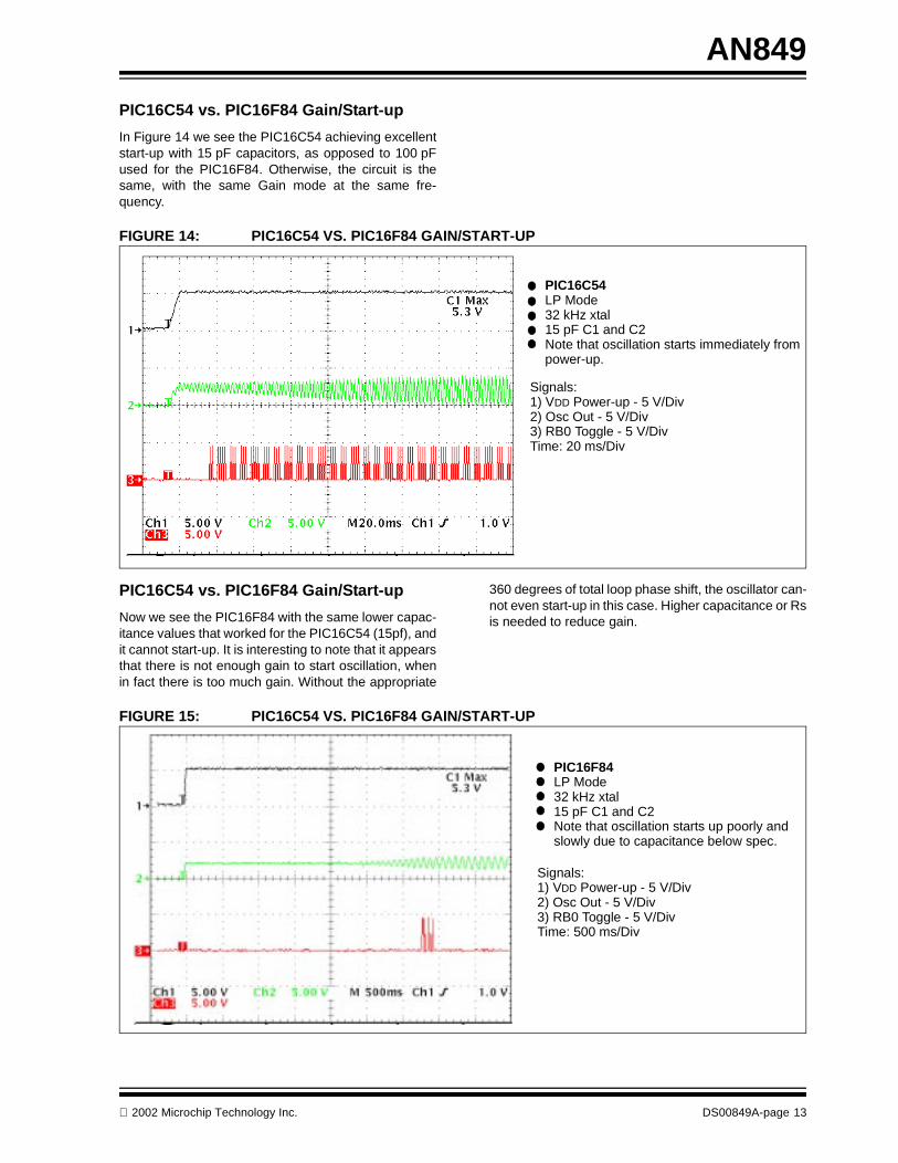
PIC16C54 vs. PIC16F84 Gain/Start-up
In Figure 14 we see the PIC16C54 achieving excellentstart-up with 15 pF capacitors, as opposed to 100 pFused for the PIC16F84. Otherwise, the circuit is thesame, with the same Gain mode at the same fre-quency.
FIGURE 14: PIC16C54 VS. PIC16F84 GAIN/START-UP
PIC16C54 vs. PIC16F84 Gain/Start-up
Now we see the PIC16F84 with the same lower capac-itance values that worked for the PIC16C54 (15pf), andit cannot start-up. It is interesting to note that it appearsthat there is not enough gain to start oscillation, whenin fact there is too much gain. Without the appropriate
360 degrees of total loop phase shift, the oscillator can-not even start-up in this case. Higher capacitance or Rsis needed to reduce gain.
FIGURE 15: PIC16C54 VS. PIC16F84 GAIN/START-UP
PIC16C54LP Mode32 kHz xtal15 pF C1 and C2Note that oscillation starts immediately frompower-up.
Signals:1) VDD Power-up - 5 V/Div2) Osc Out - 5 V/Div3) RB0 Toggle - 5 V/DivTime: 20 ms/Div
PIC16F84LP Mode32 kHz xtal15 pF C1 and C2Note that oscillation starts up poorly and
Signals:1) VDD Power-up - 5 V/Div2) Osc Out - 5 V/Div3) RB0 Toggle - 5 V/DivTime: 500 ms/Div
slowly due to capacitance below spec.
2002 Microchip Technology Inc. DS00849A-page 13

AN849
Capacitor Selection - Low VP-P
Here we demonstrate in a progression of capacitanceincreases the effects on oscillator peak-to-peak swing(see Figure 16). We increase capacitance until weachieve satisfactory margin peak-to-peak. Here wehave started with a fairly low value of 15 pF capacitors.
FIGURE 16: CAPACITOR SELECTION - LOW VP-P
Capacitor Selection - Start-Up Improved
In Figure 17, we increase to 33 pF and see an improve-ment. Again, notice that it appears as though there isnot enough gain. Too much gain means not enough
phase shift, which means the signal does not arriveback at the input at the proper moment to achieve max-imum amplification. So in fact, it IS a low gain situation,caused by too much gain!
FIGURE 17: CAPACITOR SELECTION - START-UP IMPROVED
PIC16F84LP Mode32 kHz xtal15 pF C1 and C2Oscillation is less than ideal at about2.5 VP-P due to incorrect C, spec is 100 pF
Signals:1) VDD Power-up - 5 V/Div2) Osc Out - 5 V/Div3) RB0 Toggle - 5 V/DivTime: 10 µs/Div
PIC16F84LP Mode32 kHz xtal33 pF C1 and C2Note that oscillation starts immediately frompower-up. VP-P is still less than ideal at about3 VP-P.
Signals:1) VDD Power-up - 5 V/Div2) Osc Out - 5 V/Div3) RB0 Toggle - 5 V/DivTime: 5 ms/Div
DS00849A-page 14 2002 Microchip Technology Inc.
AN849
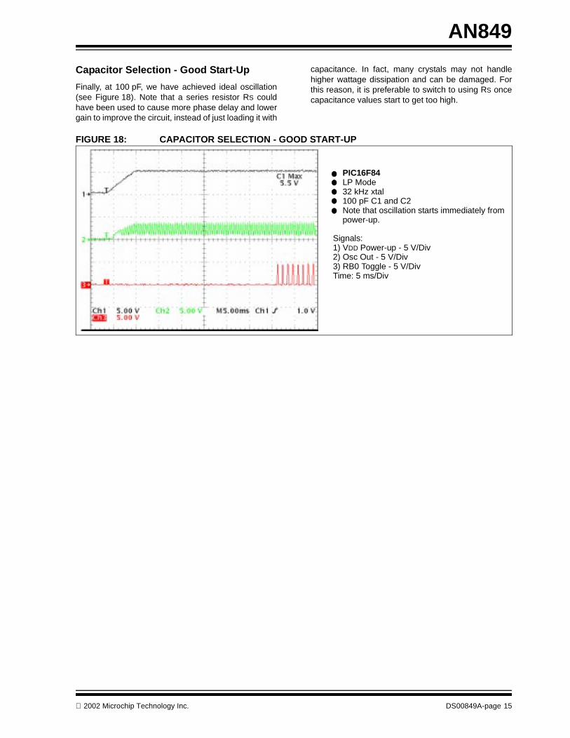
Capacitor Selection - Good Start-Up
Finally, at 100 pF, we have achieved ideal oscillation(see Figure 18). Note that a series resistor RS couldhave been used to cause more phase delay and lowergain to improve the circuit, instead of just loading it with
capacitance. In fact, many crystals may not handlehigher wattage dissipation and can be damaged. Forthis reason, it is preferable to switch to using RS oncecapacitance values start to get too high.
FIGURE 18: CAPACITOR SELECTION - GOOD START-UP
PIC16F84LP Mode32 kHz xtal100 pF C1 and C2Note that oscillation starts immediately frompower-up.
Signals:1) VDD Power-up - 5 V/Div2) Osc Out - 5 V/Div3) RB0 Toggle - 5 V/DivTime: 5 ms/Div
2002 Microchip Technology Inc. DS00849A-page 15
AN849
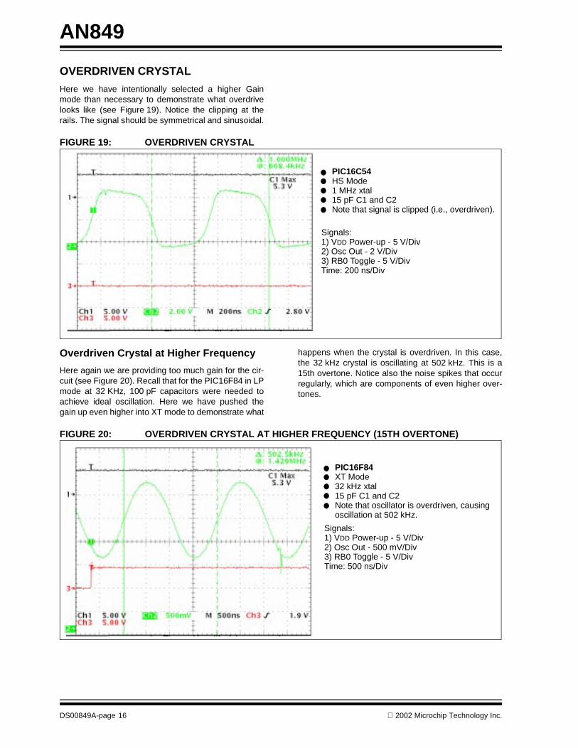
OVERDRIVEN CRYSTAL
Here we have intentionally selected a higher Gainmode than necessary to demonstrate what overdrivelooks like (see Figure 19). Notice the clipping at therails. The signal should be symmetrical and sinusoidal.
FIGURE 19: OVERDRIVEN CRYSTAL
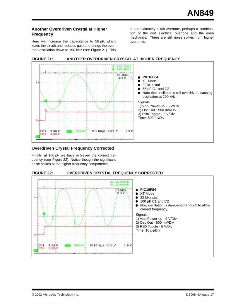
Overdriven Crystal at Higher Frequency
Here again we are providing too much gain for the cir-cuit (see Figure 20). Recall that for the PIC16F84 in LPmode at 32 KHz, 100 pF capacitors were needed toachieve ideal oscillation. Here we have pushed thegain up even higher into XT mode to demonstrate what
happens when the crystal is overdriven. In this case,the 32 kHz crystal is oscillating at 502 kHz. This is a15th overtone. Notice also the noise spikes that occurregularly, which are components of even higher over-tones.
FIGURE 20: OVERDRIVEN CRYSTAL AT HIGHER FREQUENCY (15TH OVERTONE)
PIC16C54HS Mode1 MHz xtal15 pF C1 and C2Note that signal is clipped (i.e., overdriven).
Signals:1) VDD Power-up - 5 V/Div2) Osc Out - 2 V/Div3) RB0 Toggle - 5 V/DivTime: 200 ns/Div
PIC16F84XT Mode32 kHz xtal15 pF C1 and C2Note that oscillator is overdriven, causing
Signals:1) VDD Power-up - 5 V/Div2) Osc Out - 500 mV/Div3) RB0 Toggle - 5 V/DivTime: 500 ns/Div
oscillation at 502 kHz.
DS00849A-page 16 2002 Microchip Technology Inc.
AN849
Another Overdriven Crystal at Higher Frequency
Here we increase the capacitance to 56 pF, whichloads the circuit and reduces gain and brings the over-tone oscillation down to 190 kHz (see Figure 21). This
is approximately a 6th overtone, perhaps a combina-tion of the odd electrical overtone and the evenmechanical. There are still noise spikes from higherovertones.
FIGURE 21: ANOTHER OVERDRIVEN CRYSTAL AT HIGHER FREQUENCY
Overdriven Crystal Frequency Corrected
Finally, at 100 pF we have achieved the correct fre-quency (see Figure 22). Notice though the significantnoise spikes at the higher frequency components.
FIGURE 22: OVERDRIVEN CRYSTAL FREQUENCY CORRECTED
PIC16F84XT Mode32 kHz xtal56 pF C1 and C2Note that oscillator is still overdriven, causing
Signals:1) VDD Power-up - 5 V/Div2) Osc Out - 500 mV/Div3) RB0 Toggle - 5 V/DivTime: 500 ns/Div
oscillation at 190 kHz.
PIC16F84XT Mode32 kHz xtal100 pF C1 and C2Now oscillation is dampened enough to allow
Signals:1) VDD Power-up - 5 V/Div2) Osc Out - 500 mV/Div3) RB0 Toggle - 5 V/DivTime: 10 µs/Div
correct frequency.
2002 Microchip Technology Inc. DS00849A-page 17
AN849
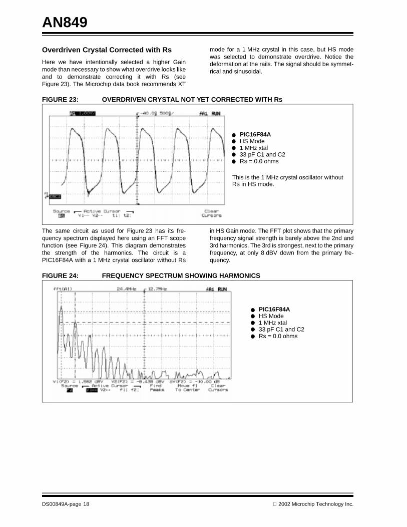
Overdriven Crystal Corrected with Rs
Here we have intentionally selected a higher Gainmode than necessary to show what overdrive looks likeand to demonstrate correcting it with Rs (seeFigure 23). The Microchip data book recommends XT
mode for a 1 MHz crystal in this case, but HS modewas selected to demonstrate overdrive. Notice thedeformation at the rails. The signal should be symmet-rical and sinusoidal.
FIGURE 23: OVERDRIVEN CRYSTAL NOT YET CORRECTED WITH RS
The same circuit as used for Figure 23 has its fre-quency spectrum displayed here using an FFT scopefunction (see Figure 24). This diagram demonstratesthe strength of the harmonics. The circuit is aPIC16F84A with a 1 MHz crystal oscillator without RS
in HS Gain mode. The FFT plot shows that the primaryfrequency signal strength is barely above the 2nd and3rd harmonics. The 3rd is strongest, next to the primaryfrequency, at only 8 dBV down from the primary fre-quency.
FIGURE 24: FREQUENCY SPECTRUM SHOWING HARMONICS
PIC16F84AHS Mode1 MHz xtal33 pF C1 and C2RS = 0.0 ohms
This is the 1 MHz crystal oscillator withoutRS in HS mode.
PIC16F84AHS Mode1 MHz xtal33 pF C1 and C2Rs = 0.0 ohms
DS00849A-page 18 2002 Microchip Technology Inc.
AN849
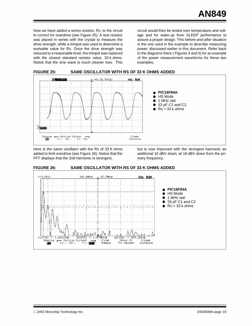
Now we have added a series resistor, RS, to the circuitto correct for overdrive (see Figure 25). A test resistorwas placed in series with the crystal to measure thedrive strength, while a trimpot was used to determine aworkable value for RS. Once the drive strength wasreduced to a reasonable level, the trimpot was replacedwith the closest standard resistor value, 33 k ohms.Notice that the sine wave is much cleaner now. This
circuit would then be tested over temperature and volt-age and for wake-up from SLEEP performance toassure a proper design. This before-and-after situationis the one used in the example to describe measuringpower, discussed earlier in this document. Refer backto the diagrams there ( Figures 4 and 5) for an exampleof the power measurement waveforms for these twoexamples.
FIGURE 25: SAME OSCILLATOR WITH RS OF 33 K OHMS ADDED
Here is the same oscillator with the RS of 33 K ohmsadded to limit overdrive (see Figure 26). Notice that theFFT displays that the 2nd harmonic is strongest,
but is now improved with the strongest harmonic anadditional 10 dBV down, at 18 dBV down from the pri-mary frequency.
FIGURE 26: SAME OSCILLATOR WITH RS OF 33 K OHMS ADDED
PIC16F84AHS Mode1 MHz xtal33 pF C1 and C2Rs = 33 k ohms
PIC16F84AHS Mode1 MHz xtal33 pF C1 and C2RS = 33 k ohms
2002 Microchip Technology Inc. DS00849A-page 19
AN849
DEMONSTRATING OSCILLATOR PERFORMANCE OVER TEMPERATURE
• A Circuit was created with low gain and marginal oscillator performance of 2.5V peak-to-peak at room temperature.
• The result is code that executes at room tempera-ture, but does not function properly at higher tem-peratures.
• At higher temperatures gain is decreased in the oscillator circuit, due in part to increased RDSON in the FETs.
• At colder temperatures, FET RDSON decreases and loop gain is increased.
• Temperature can often be used to model the effects of voltage change (and vice versa). This is because lower voltage reacts similarly to higher temperature, as both decrease gain. Conversely, higher voltages and lower temperatures both increase gain.
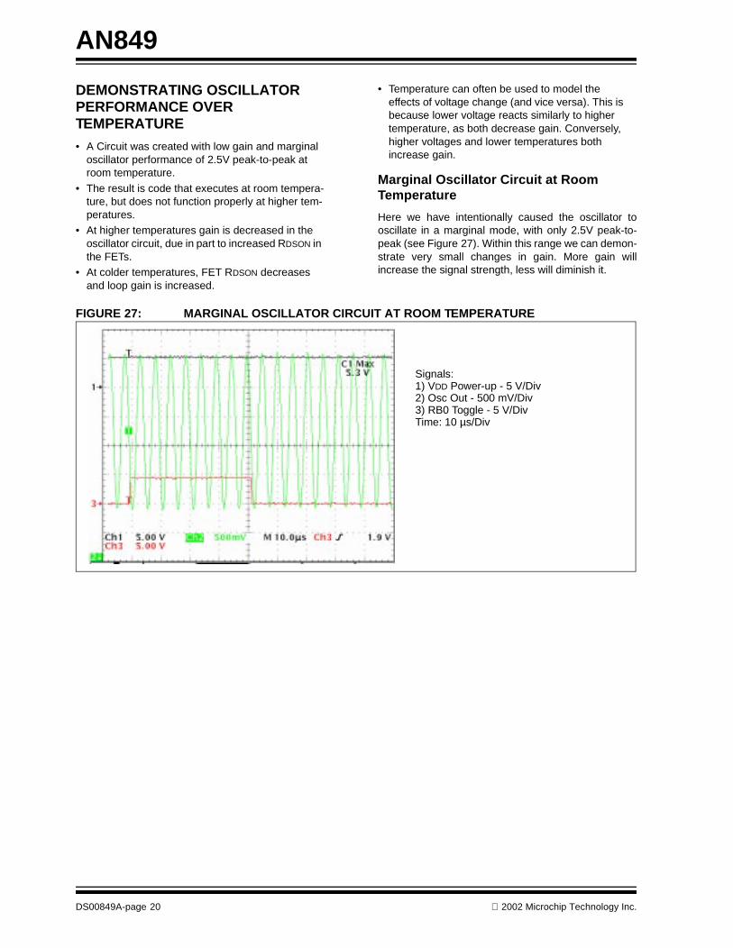
Marginal Oscillator Circuit at Room Temperature
Here we have intentionally caused the oscillator tooscillate in a marginal mode, with only 2.5V peak-to-peak (see Figure 27). Within this range we can demon-strate very small changes in gain. More gain willincrease the signal strength, less will diminish it.
FIGURE 27: MARGINAL OSCILLATOR CIRCUIT AT ROOM TEMPERATURE
Signals:1) VDD Power-up - 5 V/Div2) Osc Out - 500 mV/Div3) RB0 Toggle - 5 V/DivTime: 10 µs/Div
DS00849A-page 20 2002 Microchip Technology Inc.
AN849
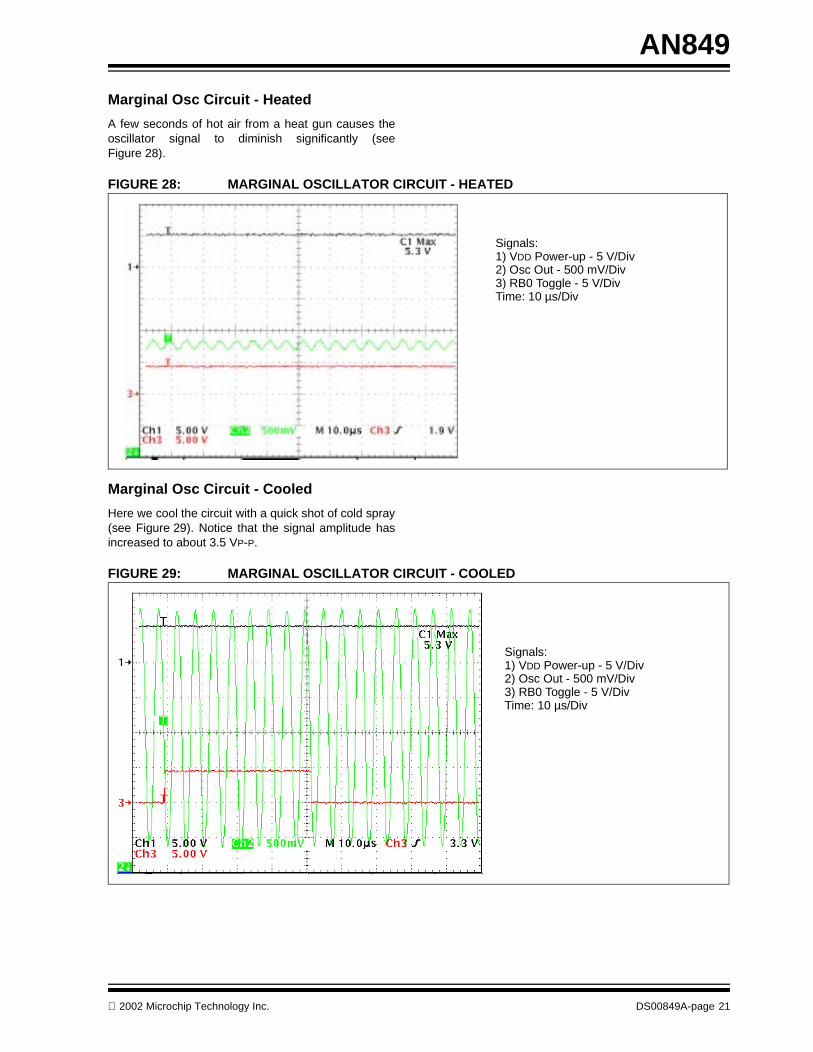
Marginal Osc Circuit - Heated
A few seconds of hot air from a heat gun causes theoscillator signal to diminish significantly (seeFigure 28).
FIGURE 28: MARGINAL OSCILLATOR CIRCUIT - HEATED
Marginal Osc Circuit - Cooled
Here we cool the circuit with a quick shot of cold spray(see Figure 29). Notice that the signal amplitude hasincreased to about 3.5 VP-P.
FIGURE 29: MARGINAL OSCILLATOR CIRCUIT - COOLED
Signals:1) VDD Power-up - 5 V/Div2) Osc Out - 500 mV/Div3) RB0 Toggle - 5 V/DivTime: 10 µs/Div
Signals:1) VDD Power-up - 5 V/Div2) Osc Out - 500 mV/Div3) RB0 Toggle - 5 V/DivTime: 10 µs/Div
2002 Microchip Technology Inc. DS00849A-page 21
AN849
Good VP-P at High and Low Temperature
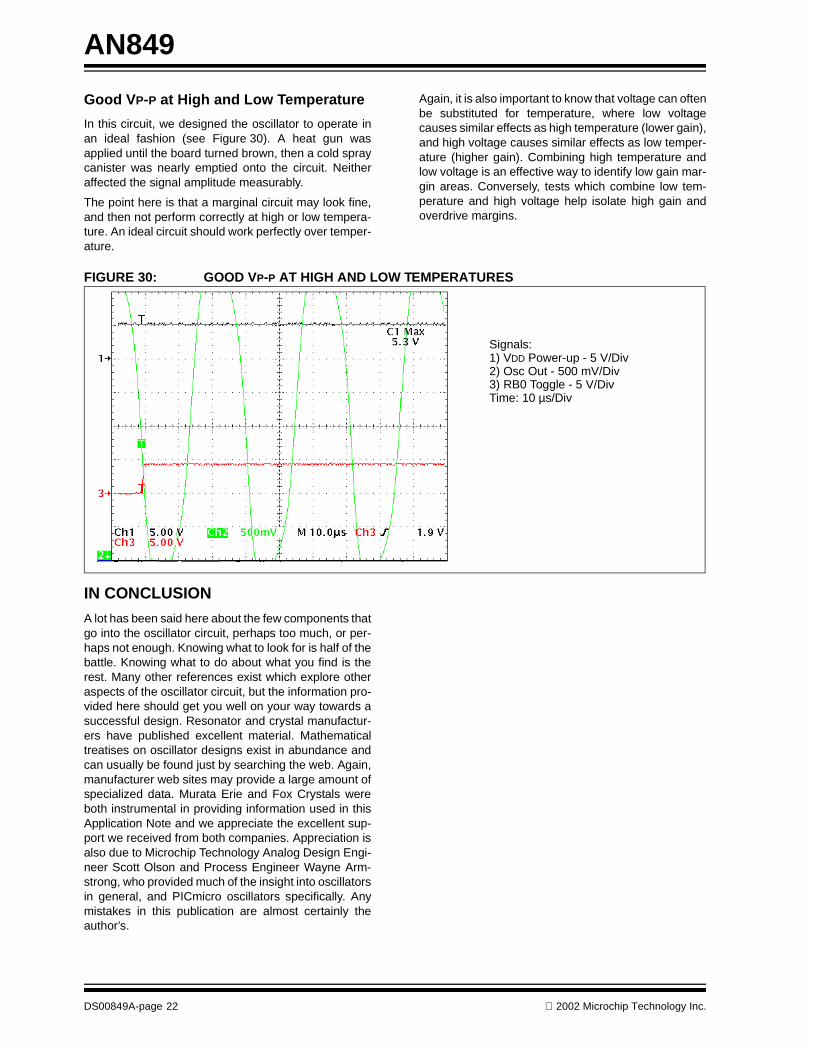
In this circuit, we designed the oscillator to operate inan ideal fashion (see Figure 30). A heat gun wasapplied until the board turned brown, then a cold spraycanister was nearly emptied onto the circuit. Neitheraffected the signal amplitude measurably.
The point here is that a marginal circuit may look fine,and then not perform correctly at high or low tempera-ture. An ideal circuit should work perfectly over temper-ature.
Again, it is also important to know that voltage can oftenbe substituted for temperature, where low voltagecauses similar effects as high temperature (lower gain),and high voltage causes similar effects as low temper-ature (higher gain). Combining high temperature andlow voltage is an effective way to identify low gain mar-gin areas. Conversely, tests which combine low tem-perature and high voltage help isolate high gain andoverdrive margins.
FIGURE 30: GOOD VP-P AT HIGH AND LOW TEMPERATURES
IN CONCLUSION
A lot has been said here about the few components thatgo into the oscillator circuit, perhaps too much, or per-haps not enough. Knowing what to look for is half of thebattle. Knowing what to do about what you find is therest. Many other references exist which explore otheraspects of the oscillator circuit, but the information pro-vided here should get you well on your way towards asuccessful design. Resonator and crystal manufactur-ers have published excellent material. Mathematicaltreatises on oscillator designs exist in abundance andcan usually be found just by searching the web. Again,manufacturer web sites may provide a large amount ofspecialized data. Murata Erie and Fox Crystals wereboth instrumental in providing information used in thisApplication Note and we appreciate the excellent sup-port we received from both companies. Appreciation isalso due to Microchip Technology Analog Design Engi-neer Scott Olson and Process Engineer Wayne Arm-strong, who provided much of the insight into oscillatorsin general, and PICmicro oscillators specifically. Anymistakes in this publication are almost certainly theauthor’s.
Signals:1) VDD Power-up - 5 V/Div2) Osc Out - 500 mV/Div3) RB0 Toggle - 5 V/DivTime: 10 µs/Div
DS00849A-page 22 2002 Microchip Technology Inc.

Note the following details of the code protection feature on PICmicro® MCUs.
• The PICmicro family meets the specifications contained in the Microchip Data Sheet.• Microchip believes that its family of PICmicro microcontrollers is one of the most secure products of its kind on the market today,
when used in the intended manner and under normal conditions.• There are dishonest and possibly illegal methods used to breach the code protection feature. All of these methods, to our knowl-
edge, require using the PICmicro microcontroller in a manner outside the operating specifications contained in the data sheet. The person doing so may be engaged in theft of intellectual property.
• Microchip is willing to work with the customer who is concerned about the integrity of their code.• Neither Microchip nor any other semiconductor manufacturer can guarantee the security of their code. Code protection does not
mean that we are guaranteeing the product as “unbreakable”.• Code protection is constantly evolving. We at Microchip are committed to continuously improving the code protection features of
our product.
If you have any further questions about this matter, please contact the local sales office nearest to you.
Information contained in this publication regarding deviceapplications and the like is intended through suggestion onlyand may be superseded by updates. It is your responsibility toensure that your application meets with your specifications.No representation or warranty is given and no liability isassumed by Microchip Technology Incorporated with respectto the accuracy or use of such information, or infringement ofpatents or other intellectual property rights arising from suchuse or otherwise. Use of Microchip’s products as critical com-ponents in life support systems is not authorized except withexpress written approval by Microchip. No licenses are con-veyed, implicitly or otherwise, under any intellectual propertyrights.
2002 Microchip Technology Inc.
Trademarks
The Microchip name and logo, the Microchip logo, KEELOQ,MPLAB, PIC, PICmicro, PICSTART and PRO MATE areregistered trademarks of Microchip Technology Incorporatedin the U.S.A. and other countries.
FilterLab, microID, MXDEV, MXLAB, PICMASTER, SEEVALand The Embedded Control Solutions Company areregistered trademarks of Microchip Technology Incorporatedin the U.S.A.
dsPIC, dsPICDEM.net, ECONOMONITOR, FanSense,FlexROM, fuzzyLAB, In-Circuit Serial Programming, ICSP,ICEPIC, microPort, Migratable Memory, MPASM, MPLIB,MPLINK, MPSIM, PICC, PICDEM, PICDEM.net, rfPIC, SelectMode and Total Endurance are trademarks of MicrochipTechnology Incorporated in the U.S.A. and other countries.
Serialized Quick Turn Programming (SQTP) is a service markof Microchip Technology Incorporated in the U.S.A.
All other trademarks mentioned herein are property of theirrespective companies.
© 2002, Microchip Technology Incorporated, Printed in theU.S.A., All Rights Reserved.
Printed on recycled paper.
DS00849A - page 23
Microchip received QS-9000 quality system certification for its worldwide headquarters, design and wafer fabrication facilities in Chandler and Tempe, Arizona in July 1999 and Mountain View, California in March 2002. The Company’s quality system processes and procedures are QS-9000 compliant for its PICmicro® 8-bit MCUs, KEELOQ® code hopping devices, Serial EEPROMs, microperipherals, non-volatile memory and analog products. In addition, Microchip’s quality system for the design and manufacture of development systems is ISO 9001 certified.
DS00849A-page 24 2002 Microchip Technology Inc.
AMERICASCorporate Office2355 West Chandler Blvd.Chandler, AZ 85224-6199Tel: 480-792-7200 Fax: 480-792-7277Technical Support: 480-792-7627Web Address: http://www.microchip.comRocky Mountain2355 West Chandler Blvd.Chandler, AZ 85224-6199Tel: 480-792-7966 Fax: 480-792-4338
Atlanta500 Sugar Mill Road, Suite 200BAtlanta, GA 30350Tel: 770-640-0034 Fax: 770-640-0307Boston2 Lan Drive, Suite 120Westford, MA 01886Tel: 978-692-3848 Fax: 978-692-3821Chicago333 Pierce Road, Suite 180Itasca, IL 60143Tel: 630-285-0071 Fax: 630-285-0075Dallas4570 Westgrove Drive, Suite 160Addison, TX 75001Tel: 972-818-7423 Fax: 972-818-2924DetroitTri-Atria Office Building 32255 Northwestern Highway, Suite 190Farmington Hills, MI 48334Tel: 248-538-2250 Fax: 248-538-2260Kokomo2767 S. Albright Road Kokomo, Indiana 46902Tel: 765-864-8360 Fax: 765-864-8387Los Angeles18201 Von Karman, Suite 1090Irvine, CA 92612Tel: 949-263-1888 Fax: 949-263-1338New York150 Motor Parkway, Suite 202Hauppauge, NY 11788Tel: 631-273-5305 Fax: 631-273-5335San JoseMicrochip Technology Inc.2107 North First Street, Suite 590San Jose, CA 95131Tel: 408-436-7950 Fax: 408-436-7955Toronto6285 Northam Drive, Suite 108Mississauga, Ontario L4V 1X5, CanadaTel: 905-673-0699 Fax: 905-673-6509
ASIA/PACIFICAustraliaMicrochip Technology Australia Pty LtdSuite 22, 41 Rawson StreetEpping 2121, NSWAustraliaTel: 61-2-9868-6733 Fax: 61-2-9868-6755China - BeijingMicrochip Technology Consulting (Shanghai)Co., Ltd., Beijing Liaison OfficeUnit 915Bei Hai Wan Tai Bldg.No. 6 Chaoyangmen Beidajie Beijing, 100027, No. ChinaTel: 86-10-85282100 Fax: 86-10-85282104China - ChengduMicrochip Technology Consulting (Shanghai)Co., Ltd., Chengdu Liaison OfficeRm. 2401, 24th Floor, Ming Xing Financial TowerNo. 88 TIDU StreetChengdu 610016, ChinaTel: 86-28-86766200 Fax: 86-28-86766599China - FuzhouMicrochip Technology Consulting (Shanghai)Co., Ltd., Fuzhou Liaison OfficeUnit 28F, World Trade PlazaNo. 71 Wusi RoadFuzhou 350001, ChinaTel: 86-591-7503506 Fax: 86-591-7503521China - ShanghaiMicrochip Technology Consulting (Shanghai)Co., Ltd.Room 701, Bldg. BFar East International PlazaNo. 317 Xian Xia RoadShanghai, 200051Tel: 86-21-6275-5700 Fax: 86-21-6275-5060China - ShenzhenMicrochip Technology Consulting (Shanghai)Co., Ltd., Shenzhen Liaison OfficeRm. 1315, 13/F, Shenzhen Kerry Centre,Renminnan LuShenzhen 518001, ChinaTel: 86-755-82350361 Fax: 86-755-82366086China - Hong Kong SARMicrochip Technology Hongkong Ltd.Unit 901-6, Tower 2, Metroplaza223 Hing Fong RoadKwai Fong, N.T., Hong KongTel: 852-2401-1200 Fax: 852-2401-3431IndiaMicrochip Technology Inc.India Liaison OfficeDivyasree Chambers1 Floor, Wing A (A3/A4)No. 11, O’Shaugnessey RoadBangalore, 560 025, IndiaTel: 91-80-2290061 Fax: 91-80-2290062
JapanMicrochip Technology Japan K.K.Benex S-1 6F3-18-20, ShinyokohamaKohoku-Ku, Yokohama-shiKanagawa, 222-0033, JapanTel: 81-45-471- 6166 Fax: 81-45-471-6122KoreaMicrochip Technology Korea168-1, Youngbo Bldg. 3 FloorSamsung-Dong, Kangnam-KuSeoul, Korea 135-882Tel: 82-2-554-7200 Fax: 82-2-558-5934SingaporeMicrochip Technology Singapore Pte Ltd.200 Middle Road#07-02 Prime CentreSingapore, 188980Tel: 65-6334-8870 Fax: 65-6334-8850TaiwanMicrochip Technology (Barbados) Inc., Taiwan Branch11F-3, No. 207Tung Hua North RoadTaipei, 105, TaiwanTel: 886-2-2717-7175 Fax: 886-2-2545-0139
EUROPEAustriaMicrochip Technology Austria GmbHDurisolstrasse 2A-4600 WelsAustriaTel: 43-7242-2244-399Fax: 43-7242-2244-393DenmarkMicrochip Technology Nordic ApSRegus Business CentreLautrup hoj 1-3Ballerup DK-2750 DenmarkTel: 45 4420 9895 Fax: 45 4420 9910FranceMicrochip Technology SARLParc d’Activite du Moulin de Massy43 Rue du Saule TrapuBatiment A - ler Etage91300 Massy, FranceTel: 33-1-69-53-63-20 Fax: 33-1-69-30-90-79GermanyMicrochip Technology GmbHSteinheilstrasse 10D-85737 Ismaning, GermanyTel: 49-89-627-144 0 Fax: 49-89-627-144-44ItalyMicrochip Technology SRLCentro Direzionale Colleoni Palazzo Taurus 1 V. Le Colleoni 120041 Agrate BrianzaMilan, Italy Tel: 39-039-65791-1 Fax: 39-039-6899883United KingdomMicrochip Ltd.505 Eskdale RoadWinnersh TriangleWokingham Berkshire, England RG41 5TUTel: 44 118 921 5869 Fax: 44-118 921-5820
08/01/02
WORLDWIDE SALES AND SERVICE