analog-digital - milwaukee area technical collegeecampus.matc.edu/lokkenr/elctec-131/pp...
TRANSCRIPT

Analog-DigitalELCTEC-131

Analog-to-Digital Conversion
Uses a circuit that converts an analog signal at its input to a digital code.
Called an A-to-D converter, A/D converter, or ADC.
2/15/2010 © 2009 Richard Lokken 2

Unipolar ADC
Converts positive input voltages.
Generates a 2n-bit binary code for any given input voltage.
2/15/2010 © 2009 Richard Lokken 3

Unipolar ADC Code Equation
Va = analog input voltage to be sampled.
FS = Full scale range of input voltage.
n = number of bits in the output code.
2/15/2010 © 2009 Richard Lokken 4
n2 FSV code a ×=
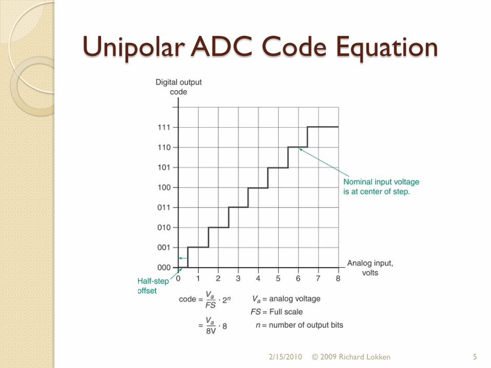
Unipolar ADC Code Equation
2/15/2010 © 2009 Richard Lokken 5

Unipolar ADC Output Codes
2/15/2010 © 2009 Richard Lokken 6
Nominal Voltage of Input Step (volts) Range (volts) Output Code0.0 0.0 - 0.5 0001.0 0.5 - 1.5 0012.0 1.5 - 2.5 0103.0 2.5 - 3.5 0114.0 3.5 - 4.5 1005.0 4.5 - 5.5 1016.0 5.5 - 6.5 1107.0 6.5 - 8.0 111

Bipolar ADC (Offset Binary Coding)
Used to represent positive and negative input voltages.
Output code an unsigned binary number.
◦ Numbers below 0 V are negative.
◦ Numbers above 0 V are positive.
2/15/2010 © 2009 Richard Lokken 7

Bipolar ADC (Offset Binary Coding)
2/15/2010 © 2009 Richard Lokken 8

Bipolar ADC Code Equation
2/15/2010 © 2009 Richard Lokken 9
222
FSV
offset 2 FSV code
a
a
nn
n
+
×=
+
×=

Bipolar ADC Output Codes
2/15/2010 © 2009 Richard Lokken 10
- 4.0 - 4.0 to - 3.5 000- 3.0 - 3.5 to - 2.5 001- 2.0 - 2.5 to - 1.5 010- 1.0 - 1.5 to - 0.5 011
0 - 0.5 to + 0.5 100+ 1.0 + 0.5 to + 1.5 101+ 2.0 + 1.5 to + 2.5 110+ 3.0 + 2.5 to + 4.0 111

Bipolar ADC (2’s Complement Coding)
Uses a 2’s complement number system.
Most significant bit (MSB) is the sign bit.
◦ MSB = ‘0’ sign positive.
◦ MSB = ‘1’ sign negative.
2/15/2010 © 2009 Richard Lokken 11

2’s Complement Output Codes
2/15/2010 © 2009 Richard Lokken 12
Nominal Voltage of Input Step (volts) Range (volts) Output Code- 4.0 - 4.0 to - 3.5 100- 3.0 - 3.5 to - 2.5 101- 2.0 - 2.5 to - 1.5 110- 1.0 - 1.5 to - 0.5 111
0 - 0.5 to + 0.5 000+ 1.0 + 0.5 to + 1.5 001+ 2.0 + 1.5 to + 2.5 010+ 3.0 + 2.5 to + 4.0 011


Flash ADC
Uses a resistive voltage divider, comparators, and a priority encoder to produce a digital code.
Conversion occurs in one clock cycle (fastest conversion time).
2/15/2010 © 2009 Richard Lokken 14

Flash ADC
2/15/2010 © 2009 Richard Lokken 15

Flash ADC
2/15/2010 © 2009 Richard Lokken 16

Disadvantage of Flash ADC
Requires 2n resistors and 2n – 1 comparators for an n-bit output.
For any large number of bits, the circuit becomes overly complex.
2/15/2010 © 2009 Richard Lokken 17

Successive Approximation ADC
The most widely used ADC.
Finds the digital representation using a “binary search.”
Also called a SAR.
2/15/2010 © 2009 Richard Lokken 18

Binary Search
1. Set the MSB of the digital representation to 1, all other bits to 0.
2/15/2010 © 2009 Richard Lokken 19

Binary Search2. Compare the analog value produced in the
first step to the voltage being converted.
a) If the test voltage is higher than the voltage being converted, reset the MSB and set the second MSB.
b) If the test voltage is less than the voltage being converted, leave the MSB set and set the second MSB.
3. Repeat Steps 2, 2A, and 2B until all the bits have been tested.
2/15/2010 © 2009 Richard Lokken 20

Binary Search
2/15/2010 © 2009 Richard Lokken 21

Binary Search – 4
2/15/2010 © 2009 Richard Lokken 22

Binary Search
2/15/2010 © 2009 Richard Lokken 23

SAR - ADC Characteristics
Final answer is always less than the input voltage.
Conversion always requires a fixed number of clock cycles.
Conversion requires n clock cycles where n is the number of bits in the digital representation.
2/15/2010 © 2009 Richard Lokken 24

Dual Slope ADC
Based on an integrator, a circuit whose output is the accumulated sum of all previous input values.
Circuit relies on storing charge representing current flow in a capacitor.
2/15/2010 © 2009 Richard Lokken 25

Dual Slope ADC Characteristics
High accuracy.
Relatively slow conversion time.
2/15/2010 © 2009 Richard Lokken 26

Dual Slope ADC Characteristics
2/15/2010 © 2009 Richard Lokken 27

Dual Slope ADC Characteristics
2/15/2010 © 2009 Richard Lokken 28

ADC0808 IC ADC
Successive approximation ADC.
Able to convert analog information from up to 8 (multiplexed) channels.
Can form the basis of a data acquisition network.
292/15/2010 © 2009 Richard Lokken

ADC0808 IC ADC
START conversion with HIGH pulse.
Conversion process driven by the clock.
End-of-conversion indicated by a HIGH on EOC.
2/15/2010 © 2009 Richard Lokken 30

ADC0808 IC ADC
Making OE HIGH allows the digital output to be read.
When OE inactive, outputs in Hi-Z state.

ADC0808 IC ADC
2/15/2010 © 2009 Richard Lokken 32