apm1688 802.11b/g/n wifi module - apmcomm.com · apm1688 802.11b/g/n wifi module description with a...
TRANSCRIPT

apm1688 802.11b/g/n WiFi Module datasheet Pre- Product Information
Page 1 of 21
1 apm Communication, Inc. – TEL: 886-3-666-1188 – FAX: 886-3-666-8033 Website: http://www.apmcomm.com – E-mail: [email protected] apmcomm Proprietary and Confidential – Product information is subject to change without notice.–Jan 10, 2014
apm1688 802.11b/g/n WiFi Module DESCRIPTION
With a small form factor of 20.2 x 20.2 x 1.85mm,the apm1688 is a full-featured WiFi 802.11b/g/n WiFi single system module that includes support for high linear output power, IEEE 802.11i security, IEEE 802.11e QoS,. By providing SDIO (1-bit, 4-bit) host interface combined with support for Linux operation systems, the apm1688 enables rapid integration of WiFi technology into a variety of host devices. The pre-tested module eliminates the need to create custom WLAN designs, resulting in greatly reduced development risk,costs and time-to-market..
GENERAL FEATURES
Small footprint: 20.2x20.2x1.85 mm IEEE 802.11b/g/n compliant
APPLICATIONS
WiFi plug-in modules for non-wireless systems.
Smartphone / PDA / PDA phone / WiFi phone / DSC / DVC with WiFi connectivity.
Printer Server / Multifunctional peripheral with WiFi connectivity.
Automotive Wi-Fi. Support Bluetooth co-existence.
APPEARANCE
Support for SDIO 4-bit and 1-bit,
SD SPI and CSPI host interfaces.
EEPROM and Front end integrated.
Embedded OS supported.
Supports Access Point tethering
functionality (Soft AP).
Designed for Wi-Fi Direct..
All mandatory IEEE 802.11b modulations: 1, 2,
5.5, 11Mbps.
All IEEE 802.11g OFDM modulations: 6, 9, 12,
18, 24, 36, 48, 54Mbps.
IEEE 802.11n HT modulations MCS0-7,
20MHz, 800 and 400ns guard interval: 6.5, 7.2,
13.0, 14.4, 19.5, 21.7, 26.0, 28.9, 39.0, 43.3,
52.0, 57.8, 58.5, 65.0, 72.2Mbps.
Frequency band: 2.412 GHz to 2.472GHz .
Supports encryption WEP40/64、WEP104/128
CCMP (AES)、TKIP 、BIP.

apm1688 802.11b/g/n WiFi Module datasheet Pre- Product Information
Page 2 of 20 2apm Communication, Inc. – TEL: 886-3-666-1188 – FAX: 886-3-666-8033 Website: http://www.apmcomm.com – E-mail: [email protected] apmcomm Proprietary and Confidential – Product information is subject to change without notice.–Jan 10, 2014
REVISION HISTORY
Date Release Author Description 12-Sep-24 0.1 Fastino Initial release
13-Feb-01 0.2 Fastino Add weight and modify high
13-Oct-11 1.0 Ryan Modify min /nor / max for high and Outline drawing
and N mode Tx power
10-Jan-14 1.1 Ryan Modify Outline 、 stencil aperture 、 Recommended
Mounting Pad drawing

apm1688 802.11b/g/n WiFi Module datasheet Pre- Product Information
Page 3 of 20 3apm Communication, Inc. – TEL: 886-3-666-1188 – FAX: 886-3-666-8033 Website: http://www.apmcomm.com – E-mail: [email protected] apmcomm Proprietary and Confidential – Product information is subject to change without notice.–Jan 10, 2014
TABLE OF CONTENTS
DESCRIPTION ................................................................................................................................................................. 1
GENERAL FEATURES .................................................................................................................................................. 1
REVISION HISTORY ..................................................................................................................................................... 2
1-1 GENERAL SPECIFICATIONS........................................................................................................................ 4
1-2 BLOCK DIAGRAM................................................................................................................................................... 4
1-3 PIN OUT ..................................................................................................................................................................... 5
1-3-1 PIN ASSIGNMENT................................................................................................................................................. 5 1-3-2 PIN DESCRIPTION ................................................................................................................................................ 5
1-4 WIFI PINS .................................................................................................................................................................. 8
1-4-1 SDIO PINS........................................................................................................................................................... 8 1-4-2 DEBUG SPI PINS ................................................................................................................................................. 9 1-4-3 PIO PINS ............................................................................................................................................................. 9 1-4-4 WP PIN ................................................................................................................................................................ 9
1-5 EXTERNAL VOLTAGE SOURCE ....................................................................................................................... 10
1-5-1 WIFI RESET ....................................................................................................................................................... 10
1-6 ELECTRICAL SPECIFICATIONS....................................................................................................................... 11
1-6-1 ABSOLUTE MAXIMUM RATING ......................................................................................................................... 11 1-6-2 RECOMMENDED OPERATING CONDITIONS....................................................................................................... 11
1-7 CURRENT CONSUMPTION ................................................................................................................................. 12
1-8 RF SPECIFICATION .............................................................................................................................................. 13
2-1 OS SUPPORT & AVAILABLE DRIVERS........................................................................................................... 15
2-2 SECURITY FEATURES SUPPORTED ............................................................................................................... 15
2-3 OTHER FEATURES............................................................................................................................................... 15
3-1 ACKAGE OUTLINE ............................................................................................................................................... 16
4-1 RECOMMENDED MOUNTING PAD DESIGN (TOP VIEW)............................................................................ 18
4-2 RECOMMENDATION FOR STENCIL APERTURE IN SMT PROCESS ....................................................... 18
4-3 BAKING CONDITION RECOMMENDATION BEFORE IR REFLOW ........................................................... 20
4-4 RECOMMENDATION FOR REFLOW PROFILE .............................................................................................. 20

apm1688 802.11b/g/n WiFi Module datasheet Pre- Product Information
Page 4 of 20 4apm Communication, Inc. – TEL: 886-3-666-1188 – FAX: 886-3-666-8033 Website: http://www.apmcomm.com – E-mail: [email protected] apmcomm Proprietary and Confidential – Product information is subject to change without notice.–Jan 10, 2014
1. HARDWARE SPECIFICATION
1-1 General Specifications
Features Description
Network standard support IEEE 802.11b/g/n
Frequency band 2412 ~ 2472 MHz
Channels 1 - 13
Modulation DSSS, OFDM, DBPSK, DQPSK, CCK, 16-QAM, 64-QAM
Wireless security WPA2-Enterprise, WPA/WPA2-PSK, TKIP, WEP
Supported rates
802.11n : 6.5, 13, 19.5, 26, 39, 52, 58.5, 65 Mbps
802.11g : 6, 9, 12, 18, 24, 36, 48, 54 Mbps
802.11b : 1, 2, 5.5, 11 Mbps
Host interface SDIO
Operating temperature -40℃ to +85℃
Supply voltage 3.3V
Dimensions 20.2 x 20.2. x 1.85 mm
1-2 Block Diagram

apm1688 802.11b/g/n WiFi Module datasheet Pre- Product Information
Page 5 of 20 5apm Communication, Inc. – TEL: 886-3-666-1188 – FAX: 886-3-666-8033 Website: http://www.apmcomm.com – E-mail: [email protected] apmcomm Proprietary and Confidential – Product information is subject to change without notice.–Jan 10, 2014
1-3 Pin out
1-3-1 Pin Assignment
1-3-2 Pin Description
* I/O: Digital Input/Output, I: Digital Input, O: Digital Output, A: Analog, PU: Pull-up, PD: Pull-down
*Pin 13 WL_1V8 is only supply apm1688 module.
Pin Symbol I/O Description 1 SPI_MOSI I Debug SPI data input
2 SPI_CS I Debug SPI chip select, active low
3 GND GND -
4 SDIO_D2 I/O
SDIO 4-bit mode: Data line [bit 2]
or Read wait (optional)
SDIO 1-bit mode: Read Wait(optional)
SDIO SPI mode: Reserved
5 SDIO_D3 I/O SDIO 4-bit mode: Data line [bit 3]
SDIO 1-bit mode: Reserved

apm1688 802.11b/g/n WiFi Module datasheet Pre- Product Information
Page 6 of 20 6apm Communication, Inc. – TEL: 886-3-666-1188 – FAX: 886-3-666-8033 Website: http://www.apmcomm.com – E-mail: [email protected] apmcomm Proprietary and Confidential – Product information is subject to change without notice.–Jan 10, 2014
Pin Symbol I/O Description CSPI mode: Card Select
6 SDIO_CLK I
SDIO 4-bit mode: Clock
SDIO 1-bit mode: Clock
CSPI mode : Clock
7 SDIO_CMD I
SDIO 4-bit mode:
Command/Response
SDIO 1-bit mode:
Command/Response
CSPI mode: Data input
8 SDIO_D0 I/O
LSB data bit for SDIO interface.
SDIO 4-bit mode: Data line [bit 0]
SDIO 1-bit mode: Data line
CSPI mode: Data output
9 SDIO_D1 I/O
SDIO 4-bit mode: Data line [bit 1]
or interrupt
SDIO 1-bit mode: Interrupt
CSPI mode : Intrrupt
10 GND GND -
11 GND GND -
12 GND GND -
13 WL_1V8 Power + 1.8v output pin
(1.8v LDO is only supply for module)
14 CE_WL_1V8 I Enable 1V8 LDO ; active High
15 VDD_SDIO Power Positive supply for SDIO interface
16 GND GND -
17 VDD_PADS_PIO_0_7 Power Positive supply for SPI, RST# and
PIO[7:0]
18 GND GND -
19 3V3 Power +3.3V Input pin
20 GND GND -
21 GND GND -
22 GND GND -
23 GND GND -
24 GND GND -
25 GND GND -
apm1688 802.11b/g/n WiFi Module datasheet Pre- Product Information
Page 7 of 20 7apm Communication, Inc. – TEL: 886-3-666-1188 – FAX: 886-3-666-8033 Website: http://www.apmcomm.com – E-mail: [email protected] apmcomm Proprietary and Confidential – Product information is subject to change without notice.–Jan 10, 2014
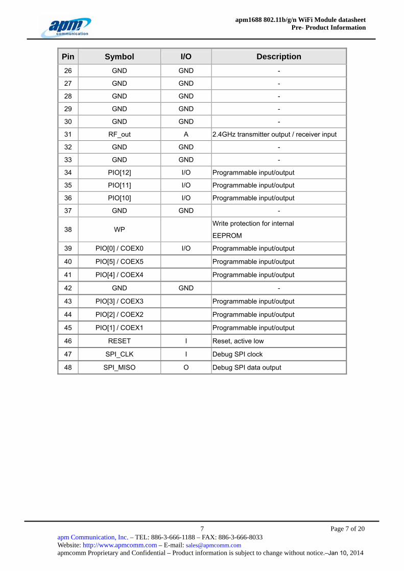
Pin Symbol I/O Description 26 GND GND -
27 GND GND -
28 GND GND -
29 GND GND -
30 GND GND -
31 RF_out A 2.4GHz transmitter output / receiver input
32 GND GND -
33 GND GND -
34 PIO[12] I/O Programmable input/output
35 PIO[11] I/O Programmable input/output
36 PIO[10] I/O Programmable input/output
37 GND GND -
38 WP Write protection for internal
EEPROM
39 PIO[0] / COEX0 I/O Programmable input/output
40 PIO[5] / COEX5 Programmable input/output
41 PIO[4] / COEX4 Programmable input/output
42 GND GND -
43 PIO[3] / COEX3 Programmable input/output
44 PIO[2] / COEX2 Programmable input/output
45 PIO[1] / COEX1 Programmable input/output
46 RESET I Reset, active low
47 SPI_CLK I Debug SPI clock
48 SPI_MISO O Debug SPI data output

apm1688 802.11b/g/n WiFi Module datasheet Pre- Product Information
Page 8 of 20 8apm Communication, Inc. – TEL: 886-3-666-1188 – FAX: 886-3-666-8033 Website: http://www.apmcomm.com – E-mail: [email protected] apmcomm Proprietary and Confidential – Product information is subject to change without notice.–Jan 10, 2014
1-4 WiFi Pins 1-4-1 SDIO Pins
apm1688 supports all defined slave modes (SD 1-bit,SD 4-bit and SDIO SPI) but not SD host
functionality.
The SDIO bus has weak internal pull up resistors on chip.
Pin # SDIO Bus Name Pin Name Description
4 DATA2 SDIO_D2
SDIO 4-bit mode: RW- Data line [bit 2] or read wait(optional)
SDIO 1-bit mode: RW- Read Wait (optional)
SDIO SPI Mode:Not used
5 DATA3 SDIO_D3
SDIO 4-bit mode: CD- Data line [bit 3] or card detect
SDIO 1-bit mode: CD- Card detect
SDIO SPI Mode:Card select(CS#)
6 CLK SDIO_CLK
SDIO 4-bit mode: Clock
SDIO 1-bit mode: Clock
SDIO SPI Mode:Clock
7 CMD SDIO_CMD
SDIO 4-bit mode: Command/Response
SDIO 1-bit mode: Command/Response
SDIO SPI Mode:Data input(MOSI)
8 DATA0 SDIO_D0
LSB data bit for SDIO interface.
SDIO 4-bit mode: Data line [bit 0]
SDIO 1-bit mode: Data line
SDIO SPI Mode:Data output(MISO)
9 DATA1 SDIO_D1
SDIO 4-bit mode: IRQ# Data line [bit 1] or interrupt (optional)
SDIO 1-bit mode: IRQ# Interrupt
SDIO SPI Mode:Interrupt(IRQ#)
apm1688 supports a SDIO device interface that conforms to the industry standard SDIO Full-Speed
card specification and allows a host controller using the SDIO bus protocol to access apm1688.

apm1688 802.11b/g/n WiFi Module datasheet Pre- Product Information
Page 9 of 20 9apm Communication, Inc. – TEL: 886-3-666-1188 – FAX: 886-3-666-8033 Website: http://www.apmcomm.com – E-mail: [email protected] apmcomm Proprietary and Confidential – Product information is subject to change without notice.–Jan 10, 2014
1-4-2 Debug SPI Pins
apm1688 has a SPI interface for test and debugging purposes. The lab tools, such as UniTest and
UniPSUtil, can communicate with apm1688 WiFi part using the SPI protocol over a connection to an LPT port.
Pin # Debug SPI Name Pin Name Description
1 MOSI SPI_MOSI Debug SPI data input
2 CS SPI_CS Debug SPI chip select, active low
47 CLK SPI_CLK Debug SPI clock
48 MISO SPI_MISO Debug SPI data output
1-4-3 PIO Pins
The PIO pins are used to implement user defined input and output signals to and from the module such
as external interrupts or other user-defined I/Os. Each PIO can be independently controlled.
PIO[12]: Host wakeup.
PIO[2:3:4:5]: BT Co-existence.
Other PIOs: Reserved.
1-4-4 WP Pin
WP is write protection for internal EEPROM. The internal EEPROM stores calibration table, MAC
address, etc. for WiFi part. When the pin is pulled high, it protects the EEPROM content. If tied to VSS, normal
memory read/write operation is enabled.
The WiFi firmware does not incorporate any support for writing to the EEPROM during normal operation.
This significantly reduces the risk of spurious writes corrupting the contents of the EEPROM, and means it is
not possible to repair any damage that may occur. Hence, it is suggested that keep the pin, WP, permanently
pulled high to minimize the risk of data corruption.

apm1688 802.11b/g/n WiFi Module datasheet Pre- Product Information
Page 10 of 20 10apm Communication, Inc. – TEL: 886-3-666-1188 – FAX: 886-3-666-8033 Website: http://www.apmcomm.com – E-mail: [email protected] apmcomm Proprietary and Confidential – Product information is subject to change without notice.–Jan 10, 2014
1-5 External Voltage Source
The external supply rails to apm1688 should have less than 10mV rms noise levels between 0 to 10
MHz. Single tone frequencies are also to be avoided. Transient response of external regulators used should
be <= 5us.
Supply voltage range
3.3V 3.3V +/-5% (ripple Vpp<10mV rms)
1-5-1 WiFi Reset
On apm1688’s main chip the pin RST# is an active-low reset input that is internally filtered using the
internal low frequency clock oscillator to avoid spurious resets. A reset occurs after the signal has been
asserted for between 250 and 375μs. This pin may be tied to VDD_PADS_PIO_0_7 if unused; otherwise it
should be asserted for at least 1ms to force a reset.
The power supply supervisor monitors VDD_DIG to trigger a POR. This occurs when the supply falls
below 1.05V (typical) in normal operation or 0.785V (typical) in deep sleep, and ends when the supply
exceeds 1.10V (typical).
Glitches of up to 30mV and 2.5μs duration, which could be caused by large load steps, will not trigger a
reset.
Each of the internal processors has its own independent watchdog timer to detect and recover from
erroneous software operation. These are typically configured with a timeout of 1.5s, but can be increased
up to a maximum of 64s for reduced power consumption.
The watchdogs are enabled at power-on and continue operating while the main chip is in deep sleep.
Following a reset, the main chip will automatically generate safe clocks for internal use. If a crystal or
external reference clock is connected to XTAL_IN then this is assumed to be at the maximum supported
frequency, otherwise the PLL free runs at a nominal frequency. In either case the generated clock is slower
than in normal operation, but this is sufficient for safely booting and configuring the main chip.
Power-on Reset Min Typ. Max Unit
Reset release on VDD_DIG rising (HI) 1.030 1.150 V Reset assert on VDD_DIG falling (LO) HI-0.060 HI-0.045 V Reset assert on VDD_DIG falling (Sleep mode) 0.77 0.785 0.800 V

apm1688 802.11b/g/n WiFi Module datasheet Pre- Product Information
Page 11 of 20 11apm Communication, Inc. – TEL: 886-3-666-1188 – FAX: 886-3-666-8033 Website: http://www.apmcomm.com – E-mail: [email protected] apmcomm Proprietary and Confidential – Product information is subject to change without notice.–Jan 10, 2014
1-6 Electrical Specifications
1-6-1 Absolute Maximum Rating
Symbol Description Min. Max. UnitsTst Storage temperature -50 105 ℃
CE_WL_1V8 Enable 1.8v LDO Regulators 1.3 5 V
VDD_SDIO Positive supply for SDIO interface 1.7 3.5 V
VDD_PADS_PIO_0_7 Positive supply for SPI, RST# and
PIO[7:0]
1.7 3.5 V
3v3 +3.3V Input pin 3 3.8 V
*Absolute maximum ratings indicate limits beyond which damage to the device may occur.
1-6-2 Recommended Operating Conditions
Symbol Description Min. Typ. Max. UnitsTop Operating temperature -40 25 85 ℃
CE_WL_1V8 Enable 1.8v LDO Regulators 1.3 3.3 5 V
VDD_SDIO Positive supply for SDIO interface 1.7 3.3 3.6 V
VDD_PADS_PIO_0_7 Positive supply for SPI, RST# and
PIO[7:0]
1.7 3.3 3.6 V
3v3 +3.3V Input pin 3 3.3 3.6 V

apm1688 802.11b/g/n WiFi Module datasheet Pre- Product Information
Page 12 of 20 12apm Communication, Inc. – TEL: 886-3-666-1188 – FAX: 886-3-666-8033 Website: http://www.apmcomm.com – E-mail: [email protected] apmcomm Proprietary and Confidential – Product information is subject to change without notice.–Jan 10, 2014
1-7 Current Consumption Conditions: 3V3= +3.3 V;TOP= 25℃;Unitest tool:V7.2.1.5
Parameter Test conditions Min. Typ. Max. Units802.11b Current Consumption
11Mbps transmit @ 17dBm
Continuous packet, PSDU length
of 1024 Bytes (958us), packet
interval 50μs
- 277 - mA
11Mbps receive
Continuous packet, PSDU length
of 1024 Bytes (179us), packet
interval 117μs
- 110 - mA
802.11g Current Consumption
54Mbps transmit @ 15dBm
Continuous packet, PSDU length
of 1024 Bytes (179us), packet
interval 117μs
- 240 - mA
54Mbps receive
Continuous packet, PSDU length
of 1024 Bytes, packet interval
50μs
- 117 - mA
802.11n Current Consumption
MCS7 transmit @ 14dBm Continuous packet, PSDU length
of 4096 Bytes - 229 - mA
MCS7 receive Continuous packet, PSDU length
of 4096 Bytes - 117 - mA
Other mode Current Consumption
Listen Current
Consumption
Receive but no CCK or OFDM
packet in air 10 mA
Deep sleep - - 133 - uA

apm1688 802.11b/g/n WiFi Module datasheet Pre- Product Information
Page 13 of 20 13apm Communication, Inc. – TEL: 886-3-666-1188 – FAX: 886-3-666-8033 Website: http://www.apmcomm.com – E-mail: [email protected] apmcomm Proprietary and Confidential – Product information is subject to change without notice.–Jan 10, 2014
1-8 RF Specification Conditions: 3V3= +3.3 V, TOP= 25℃, Unitest tool:V7.2.1.5
Parameter Test conditions Min. Typ. Max. IEEE
Specification Units
Frequency range 2400 - 2500 - MHz
Operating temperature -40 - +85 - ℃
802.11b Transmit
Transmit EVM 11Mbps @ 17dBm
Channel 1~13 4
35 %
Transmit output
power 1/2/5.5/11Mbps
15.5
17
18.5
-
dBm
Center
frequency
tolerance
11Mbps @ 17dBm
Channel 1~13
-20
20
±20
ppm
Spectral mask
@ 1st side lobe 1Mbps @ 17dBm
-
-47
-
-36
dBc
Spectral mask
@ 2nd side lobe 1Mbps @ 17dBm
-
-54
-
-50
dBc
802.11b Receive Sensitivity Minimum input
level sensitivity 11Mbps CCK, FER<8%
-86
-
-
-76
dBm
Maximum
input level
sensitivity
11Mbps CCK, FER<8%
-
-
-9
-10
dBm
802.11g Transmit
Transmit EVM 54Mbps @15dBm
Channel 1~13
-
-
-25
-25 dB
Transmit
output power
6 / 9 / 12 /18 / 24 / 36 /
48 / 54 Mbps
13.5
15
16.5
-
dBm
Center
frequency
tolerance
54Mbps @17dBm
Channel 1~13
-25
25
±25
ppm
f < fc-30, fc+30 <f - -51 - -40 dBr Spectrum Mask
fc-30 <f <fc-20, fc+20 <f

apm1688 802.11b/g/n WiFi Module datasheet Pre- Product Information
Page 14 of 20 14apm Communication, Inc. – TEL: 886-3-666-1188 – FAX: 886-3-666-8033 Website: http://www.apmcomm.com – E-mail: [email protected] apmcomm Proprietary and Confidential – Product information is subject to change without notice.–Jan 10, 2014
Parameter Test conditions Min. Typ. Max. IEEE
Specification Units
<fc+30 - -45 - -28 dBr
fc-20 <f <fc-11, fc+11 <f
<fc+20 -
-36 -
-20 dBr
fc-11 <f <fc-9, fc+9 <f
<fc+11
-
-20.3
-
- dBr
802.11g Receive Sensitivity Minimum input
level sensitivity
54Mbps OFDM,
FER<10%
-73
-
-
-65
dBm
Maximum input
level sensitivity
54Mbps OFDM,
FER<10%
-
-
-17
-20
dBm
802.11n 20MHz Transmit
Transmit EVM
65Mbps MCS7@
14dBm
Channel 1~13
-28
-
-
-28
dB
Transmit output
power
6.5 / 13 / 19.5 / 26 / 39 /
52 / 58.5 / 65 Mbps 12 13.5 15
- dBm
Center
frequency
tolerance
65Mbps MCS7@
14dBm
-25
-
25
±25 ppm
802.11n 20MHz Receive Minimum input
level sensitivity
65Mbps MCS7,
FER<10%
-70
-
-65
dBm
Maximum input
level sensitivity
65Mbps MCS7,
FER<10%
-
-
-18
-20
dBm
apm1688 802.11b/g/n WiFi Module datasheet Pre- Product Information
Page 15 of 20 15apm Communication, Inc. – TEL: 886-3-666-1188 – FAX: 886-3-666-8033 Website: http://www.apmcomm.com – E-mail: [email protected] apmcomm Proprietary and Confidential – Product information is subject to change without notice.–Jan 10, 2014
2. Software Specifications
2-1 OS Support & Available Drivers
SDIO 1 bit or 4-bit
Linux 2.6.24 and above
Android
RTOS
WinCE
2-2 Security Features Supported
Support for IEEE 802.11i security enhancements
WEP
TKIP
AES
WPA
WPA2
2-3 Other Features
Supports for IEEE 802.11d transmit power control (Regulatory Domain Support for New
Countries).
Support for IEEE 802.11e (Quality of Service): WMM and WMM Power Save.
Host wakeup signaling.

apm1688 802.11b/g/n WiFi Module datasheet Pre- Product Information
Page 16 of 20 16apm Communication, Inc. – TEL: 886-3-666-1188 – FAX: 886-3-666-8033 Website: http://www.apmcomm.com – E-mail: [email protected] apmcomm Proprietary and Confidential – Product information is subject to change without notice.–Jan 10, 2014
3. Mechanical Specifications Dimension 20.2 x 20.2 x 1.85 mm
Pin out 48
Weight 1.49g
3-1 Package Outline

apm1688 802.11b/g/n WiFi Module datasheet Pre- Product Information
Page 17 of 20 17apm Communication, Inc. – TEL: 886-3-666-1188 – FAX: 886-3-666-8033 Website: http://www.apmcomm.com – E-mail: [email protected] apmcomm Proprietary and Confidential – Product information is subject to change without notice.–Jan 10, 2014

apm1688 802.11b/g/n WiFi Module datasheet Pre- Product Information
Page 18 of 20 18apm Communication, Inc. – TEL: 886-3-666-1188 – FAX: 886-3-666-8033 Website: http://www.apmcomm.com – E-mail: [email protected] apmcomm Proprietary and Confidential – Product information is subject to change without notice.–Jan 10, 2014
4. Assembly Guideline 4-1 Recommended Mounting Pad Design (Top View)
The following figure illustrates the recommended mounting pad design for apm1688.
TOP VIEW (mm)
4-2 Recommendation for Stencil Aperture in SMT Process

apm1688 802.11b/g/n WiFi Module datasheet Pre- Product Information
Page 19 of 20 19apm Communication, Inc. – TEL: 886-3-666-1188 – FAX: 886-3-666-8033 Website: http://www.apmcomm.com – E-mail: [email protected] apmcomm Proprietary and Confidential – Product information is subject to change without notice.–Jan 10, 2014
Please follow general QFN stencil design guideline. Some rules of thumb are highlighted below.
The LGA pads should NOT be flooded over with copper; they should be connected into the plane
with a track width of approx 50% of the pad width, this will mean more heat will be available at the
joint. Track lengths should obviously be minimized, we would generally use about 0.3mm on
external layers.
The solder paste pattern for the internal Tab pads could be split into 4 smaller segments for the 2
large pads, and 2 smaller segments for the smaller pads, this should have the effect of preventing
the paste from pooling into one area, and hence minimize the likelihood of the pads being held
away from each other. We use a rule of thumb of 50% solder paste area in relation to Tab copper
area (this only applies to tab pads under the device – not the signal pads).
The thickness of the solder paste stencil has implications on solder joint quality as well, we do not
have the knowledge on what stencil should be specified.
Ensure they are using a good appropriate flux, and the correct reflow profile for unleaded (basically
+20C above leaded) which is also uniform in nature.
Violating the basic rules might cause problems. For example, if the stencil apertures of the internal
ground planes are improperly big, they would hold more solders in SMT process and may cause the module
peripheral pads un-contacted to the main board.
To improve this situation, apmcomm suggests the stencil opening shown as follows.
Stencil Aperture (Top View)

apm1688 802.11b/g/n WiFi Module datasheet Pre- Product Information
Page 20 of 20 20apm Communication, Inc. – TEL: 886-3-666-1188 – FAX: 886-3-666-8033 Website: http://www.apmcomm.com – E-mail: [email protected] apmcomm Proprietary and Confidential – Product information is subject to change without notice.–Jan 10, 2014
4-3 Baking condition recommendation before IR reflow
Baking condition for apm1688 module:
125°C/4 hrs baking is necessary for apm1688 module before SMT process. After baking treatment
the modules can be stored in the environment under 30°C and 60% RH for 168 hrs. If the storage
time is over 168 hrs, the modules need to be re-baked using the same condition again.
In the event that the sealed bag is damaged on receipt of the modules, the baking condition should
be changed to 125°C/8 hrs.
4-4 Recommendation for Reflow Profile
Maximum reflow temperature is 250°C.
Heating/Cooling Speed Pre-Heating Heating
△T1 △T2 △T3 Tp1-Tp2 tpre Tmax tp3
1 to 3℃ /sec. 1 to 3℃ /sec. < 2℃ /sec. 125 ~ 180℃ 30 ~ 90 sec. 250℃ max. 30 ~90 sec.