application note evaluation board 300w smps
TRANSCRIPT

1 Revision 1.1, 2015-10-20
About this document
Scope and purpose
The presented evaluation design is a 300 W Switch Mode Power Supply (SMPS) employing the Infineon
Combi Controller IC ICE1CS02. The system is partitioned in a Power Factor Correction section (PFC stage) and a Two-Transistor Forward section (TTF stage).
The power supply can be operated from universal input (90 VAC up to 265 VAC at 50~60 Hz) and provides a regulated output of 42 VDC. Alternatively, suggestions are given to obtain 24 VDC or different outputs.
Note: The power board is operated by a control daughterboard using ICE1CS02G. Infineon also offers an
alternative solution, using ICE3PCS01G as PFC CCM controller and LM5021-2 as TTF controller. Please see “Addendum to 300 W general purpose wide range SMPS”[7]on Infineon website.
The design originates from general purpose AC line transformer replacement in low voltage motor drive applications. The design choices are made to allow hard step loads with minimum output drop.
Attention: This board is intended for evaluation purposes only and is not intended to be an end product
Intended audience
Design engineers approaching a Switch Mode Power Supply (SMPS) intended for non continuous load conditions like implemented with Infineon’s 300 W SMPS evaluation board.
Table of contents
1 System and board description ...................................................................................... 3 1.1 Topology description .......................................................................................................................... 3
1.1.1 System protection and features ................................................................................................... 6 1.1.2 Schematic ...................................................................................................................................... 7
2 AC line input filter and bridge ....................................................................................... 9
2.1 Input filter layout ................................................................................................................................ 9 2.2 Input rectifier bridge ......................................................................................................................... 10
3 PFC stage ................................................................................................................. 11
300 W g en eral purp o se wid e -ra ng e S M PS PFC + TTF Evaluation Board
Author: Andrea Merello
Application Note

300 W general purpose wide-range SMPS PFC + TTF Evaluation Board
About this document
Application Note 2 Revision 1.1, 2015-10-20
3.1 PFC inductor design .......................................................................................................................... 11 3.2 PFC MOSFET design .......................................................................................................................... 13
3.3 PFC Shunt resistor ............................................................................................................................. 15 3.4 PFC diode design ............................................................................................................................... 16 3.5 PFC capacitor design......................................................................................................................... 16
4 TTF stage ................................................................................................................. 17
4.1 TTF primary side ................................................................................................................................ 17 4.1.1 TTF transformer .......................................................................................................................... 17
4.1.2 TTF Primary side MOSFETs ......................................................................................................... 19
4.1.3 TTF shunt resistor ....................................................................................................................... 21 4.1.4 MOSFET gate driving ................................................................................................................... 21
4.2 TTF secondary side............................................................................................................................ 23 4.2.1 TTF rectifier diodes ..................................................................................................................... 23 4.2.2 TTF output passives .................................................................................................................... 25
4.2.3 TTF feedback ............................................................................................................................... 26
5 Auxiliary power supply .............................................................................................. 28
6 Control card with ICE1CS02G ...................................................................................... 30
6.1 PFC voltage and current loop ........................................................................................................... 31
7 Converter test results ................................................................................................ 33
7.1 Converter efficiency .......................................................................................................................... 33
7.2 Converter waveforms ........................................................................................................................ 34 7.2.1 PFC plots ...................................................................................................................................... 34
7.2.2 TTF plots on primary side ........................................................................................................... 38 7.2.3 TTF plots on secondary side ....................................................................................................... 39
7.2.4 Flyback supply............................................................................................................................. 41
8 Final considerations .................................................................................................. 43
9 Bill of Material (BOM)................................................................................................. 44
10 Appendix A: Average and rms values ........................................................................... 47
10.1 Sinusoidal waveform ........................................................................................................................ 47
10.2 Rectangular pulse train ..................................................................................................................... 48 10.3 Sawtooth waveform .......................................................................................................................... 48
10.4 Triangular waveforms ....................................................................................................................... 49
11 Appendix B: Chart representation of power MOSFET losses in hard switching .................. 51
12 References and proposed links ................................................................................... 53

300 W general purpose wide-range SMPS PFC + TTF Evaluation Board
System and board description
Application Note 3 Revision 1.1, 2015-10-20
1 System and board description The presented design consists in a power supply with aim of reducing system volume and weight, while
increasing power factor, standby consumption and efficiency.
The application requirements follow in Table 1:
Table 1 Application requirements
Input 85 VAC to 265 VAC
Input power factor 95% at 150 W @220 VAC(in); 99% full load
99% at 150 W @110 VAC(in); 99% full load
Output voltage 42 V (24 V variant with changes allowed)
Output power 300 W peak
150 W continuous
Efficiency 90% typ. high-line @220 VAC(in) from 150 W
87% typ. low-line @110 VAC(in) from 150 W
Ambient Temperature Tested at 25°C ambient
Design procedure developed at 70°C ambient
The PFC stage is using Infineon’s high voltage MOSFET 600 V CoolMOS™ C6 and Infineon’s power silicon
diode technology, Rapid 2 Diode. To improve efficiency and reduce commutation noise Infineon’s thinQ!™
Generation 5 SiC Schottky Diode can be used. This stage works at a fixed frequency of 65 kHz, both in
Discontinued Conduction Mode (DCM) and Continued Conduction Mode (CCM).
The TTF stage takes benefit from 500 V CoolMOS™ CE MOSFET family. This stage works at 130 kHz in CCM mode.
This paper describes a detailed application circuit, the design choices, the PCB drawings, the oscilloscope
waveforms and the components. Furthermore, magnetics, power losses evaluation in active devices and heatsink design are included.
1.1 Topology description
The following pictures represent the board topology and it’s partitioning with indication of the main
components.
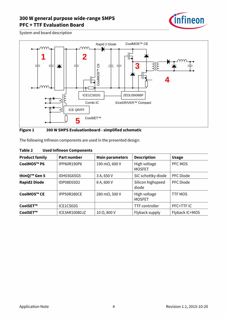
For a better explanation, the power supply can be divided into 5 parts, shown in Figure 1.
1. The input filter 2. The PFC stage 3. The TTF stage 4. The output stage
5. The auxiliary supply
300 W general purpose wide-range SMPS PFC + TTF Evaluation Board
System and board description
Application Note 4 Revision 1.1, 2015-10-20
2EDL05I06BFICE1CS02G
Rapid 2 Diode
Co
olM
OS
™ C
6
CoolMOS™ CE
Combi IC EiceDRIVER™ Compact
ICE QR/FF
1 23
4
5CoolSET™
Figure 1 300 W SMPS Evaluationboard - simplified schematic
The following Infineon components are used in the presented design:
Table 2 Used Infineon Components
Product family Part number Main parameters Description Usage
CoolMOS™ P6 IPP60R190P6 190 mΩ, 600 V High voltage
MOSFET
PFC MOS
thinQ!™ Gen 5 IDH03G65G5 3 A, 650 V SiC schottky diode PFC Diode
Rapid2 Diode IDP08E65D2 8 A, 600 V Silicon highspeed
diode PFC Diode
CoolMOS™ CE IPP50R280CE 280 mΩ, 500 V High voltage
MOSFET TTF MOS
CoolSET™ ICE1CS02G TTF controller PFC+TTF IC
CoolSET™ ICE3AR10080JZ 10 Ω, 800 V Flyback supply Flyback IC+MOS
300 W general purpose wide-range SMPS PFC + TTF Evaluation Board
System and board description
Application Note 5 Revision 1.1, 2015-10-20
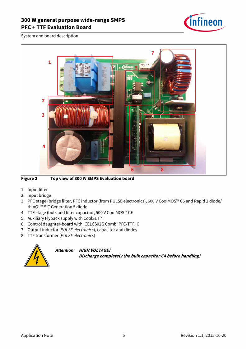
Figure 2 Top view of 300 W SMPS Evaluation board
1. Input filter 2. Input bridge
3. PFC stage (bridge filter, PFC inductor (from PULSE electronics), 600 V CoolMOS™ C6 and Rapid 2 diode/ thinQ!TM SiC Generation 5 diode
4. TTF stage (bulk and filter capacitor, 500 V CoolMOS™ CE 5. Auxiliary Flyback supply with CoolSET™
6. Control daughter-board with ICE1CS02G Combi PFC-TTF IC 7. Output inductor (PULSE electronics), capacitor and diodes
8. TTF transformer (PULSE electronics)
Attention: HIGH VOLTAGE! Discharge completely the bulk capacitor C4 before handling!

300 W general purpose wide-range SMPS PFC + TTF Evaluation Board
System and board description
Application Note 6 Revision 1.1, 2015-10-20
Figure 3 Bottom view of 300 W SMPS Evaluation board (flipped)
1. Bypass diode
2. PFC shunts 3. TTF shunts
4. TTF gate driver 2EDL05I06BF 5. TTF free-wheeling diodes
6. Auxiliary Flyback supply, ICE CoolSET™ design with Fixed Frequency @100 kHz. Quasi Resonant variant possible. GREEN LED indicates operation. When LED is off, bus voltage falls below typ. 50 V
7. TTF feedback network
8. Output rectifier diode snubber
9. Output rectifier diode snubber
1.1.1 System protection and features
The power supply is featured as follows:
PFC
Cycle-by-cycle overcurrent protection via shunt sensing
Input Brown-out protection and input under-voltage protection at start-up
Output redundant overvoltage protection (double sensing)
Enhanced dynamic response on load jumps and input mains voltage dips
Soft start of DC bus voltage to limit start-up current
Frequency synchronization with PWM TTF stage. PFC=65 kHz; TTF=130 kHz.
Programmable switching frequency by external PWM signal synchronization

300 W general purpose wide-range SMPS PFC + TTF Evaluation Board
System and board description
Application Note 7 Revision 1.1, 2015-10-20
TTF
Cycle-by-cycle overcurrent protection via shunt sensing
Output short circuit protection
Output overcurrent protection
Output overvoltage protection
Output soft start
DC bus under-voltage protection via PFC
Slope compensation and limited max duty cycle 47% (or programmable 60%)
Gate driving under-voltage lockout (UVLO) via gate driver
Minimum pulse cutout via gate driver
1.1.2 Schematic
The design consists of a Power Board and a Control Card.
Power board and control card schematics are shown respectively in Figure 4 and Figure 5.
For higher resolution, please use the schematic and layout attachment.
Figure 4 Power board schematic of 300 W SMPS Evaluationboard

300 W general purpose wide-range SMPS PFC + TTF Evaluation Board
System and board description
Application Note 8 Revision 1.1, 2015-10-20
Figure 5 Control card schematic of 300 W SMPS Evaluationboard

300 W general purpose wide-range SMPS PFC + TTF Evaluation Board
AC line input filter and bridge
Application Note 9 Revision 1.1, 2015-10-20
2 AC line input filter and bridge The input filter has been designed to cut common mode noise in the first hundreds kHz band. Highest
available values X2 common mode capacitors (C2 and C3) have been equipped, consistently with the available board space. Differential mode noise filter is not implemented. Fuse protection and surge protection has been implemented close to the input connector. 5 Ω NTC (RT1) for inrush current limitation is
provided.
Figure 6 Input filter
2.1 Input filter layout
The filter layout should be as symmetrical as possible. A general rule recommends input filter in an orthogonal placement to other magnetics, in particular the PFC coil. Our proposal follows.
Connection of GND-Earth (Pin 2 of J1 connector) must be connected to metallic enclosure to reduce common mode noise. In case there is no enclosure, Y-caps (CY1 and CY2) have to be removed.
Figure 7 Input filter placement on board
Input filter is designed pragmatically in order to minimize conducted noise. Space and footprint for a bigger common mode chocke is available as shown in Figure 8 .
When more than 2-layer board is used, the recommendation is to mount the Y-caps and extend the
GND_EARTH shield plane on the bottom layer in order to couple the switching noise back to the power GND.

300 W general purpose wide-range SMPS PFC + TTF Evaluation Board
AC line input filter and bridge
Application Note 10 Revision 1.1, 2015-10-20
Figure 8 Input filter layout on proposed design
Please note that the fuse (FUSE1) to the surge suppressor (VAR1) net should be shortened in a better layout,
in order to reduce the stray inductance path for very fast/high voltage surges from the net.
2.2 Input rectifier bridge
The proposed input bridge rectifier is a GBU8J, which is sized according to the power losses. The Power
losses are calculated at maximum output power, 300 W, and minimum input voltage, 85 VAC using simple
assumptions.
We assume that efficiency is η=85%, and forward voltage VF=0.85 V, which is the value at 4 ADC.
𝐼𝐼𝑁 (𝑟𝑚𝑠) = 𝑃𝐼𝑁
𝑉𝐼𝑁 (𝑟𝑚𝑠)=
𝑃𝑂𝑈𝑇 / 𝜂
𝑉𝐼𝑁 (𝑟𝑚𝑠)=
300 𝑊/ 0.85
85 𝑉~ 4.15 𝐴 Eq 1
𝑃𝐵𝑅1 = 2 ∙ 𝑉𝐹 ∙ 𝐼𝐼𝑁(𝑟𝑚𝑠) = 2 ∙ 0.85𝑉 ∙ 4.15𝐴 = 7 𝑊 Eq 2
Heatsinking of input bridge is necessary. Average power consumption considering the power supply duty
cycle of 5 min off/ 5 min on = 50% is 4.5 W, but temperature ripples depending on heatsink thermal inertia. With the provided heatsink, the temperature at bridge case rises up to 115°C.
Provided from GBU8J a Rth(j-c)=4.0 K/W, the junction temperature is close to 150°C at 7 W continuous load.

300 W general purpose wide-range SMPS PFC + TTF Evaluation Board
PFC stage
Application Note 11 Revision 1.1, 2015-10-20
3 PFC stage The controller provides a fixed frequency CCM PFC control algorithm. The PFC stage is designed to operate
at 65 kHz, which is the standard operating frequency generated by the controller ICE1CS02G, mounted on the daughter board.
This frequency provides a compromise between inductor ripple and switching losses. Moreover keeps the 3rd harmonic of the PFC (190 kHz) in the 1st band of the conducted emissions (EMC).
Frequency can be changed by providing a synchronization signal at SYNC pin of the controller IC (see ICE1CS02G datasheet, SYNC pin section).
The PFC stage includes a pre-charge silicon diode (D1) which is recommended when D2 is a SiC diode, to
avoid in-rush currents at hot NTC.
Figure 9 PFC stage schematic
3.1 PFC inductor design
PFC sizing is considered at maximum output power of 300 W and low line (VAC,min = 85 VAC), where input
current is maximum.
L1 has then been chosen in order to reach a maximum current ripple of
∆𝐼𝐿1,𝑚𝑎𝑥 = 20% ∙ 𝐼𝐿1,𝑚𝑎𝑥 Eq 3
Where ΔIL1,max represents the current ripple and IL1,max represents the peak average inductor current in CCM
mode.
Considering the following conditions:
Input mains voltage: 85 VAC
Input power: 300 W / 85% = 350 W

300 W general purpose wide-range SMPS PFC + TTF Evaluation Board
PFC stage
Application Note 12 Revision 1.1, 2015-10-20
𝐼𝐿1,𝑚𝑎𝑥 =𝑃𝑚𝑎𝑥 ∙ √2
𝑉𝑖𝑛,𝑚𝑖𝑛=
350𝑊 ∙ √2
85𝑉𝐴𝐶= 5.82𝐴𝑝𝑘
Eq 4
Then ΔIL1,max = 1.2 A from Eq 3.
PFC inductance value can be derived from the simplified equation below.
∆𝐼𝐿1𝑚𝑎𝑥 =𝑉𝐵𝑈𝑆 − 𝑉𝑖𝑛(𝑟𝑚𝑠)
𝐿1∙ 𝑡𝑜𝑓𝑓
𝑉𝐵𝑈𝑆
𝑉𝑖𝑛(𝑟𝑚𝑠)=
1
1 − 𝐷𝑃𝐹𝐶→ 𝐿1 =
𝑉𝐵𝑈𝑆
𝑓𝑠𝑤(𝑃𝐹𝐶) ∙ ∆𝐼𝐿1,𝑚𝑎𝑥∙ 𝐷𝑃𝐹𝐶 ∙ (1 − 𝐷𝑃𝐹𝐶)
𝐿1 =380 𝑉
65 𝑘𝐻𝑧 ∙ 1.2𝐴∙ 0.5 ∙ (1 − 0.5) = 1.2 𝑚𝐻
Eq 5
The PFC inductor is provided by PULSE Electronics (PH9297NL).
Specification follows in Figure 10.
Figure 10 PFC inductor specification, from Pulse Electronics
Figure 11 PFC inductor mechanical drawing (side)

300 W general purpose wide-range SMPS PFC + TTF Evaluation Board
PFC stage
Application Note 13 Revision 1.1, 2015-10-20
As can be seen in Figure 11, the inductor design has been segmented in 4 sub-windings.
The segmentation is made to reduce inter-winding coupling, by keeping distance between turns which have
high voltage difference. This minimizes stray inter-winding capacitance, which generates high frequency oscillations. In fact, current oscillations, superimposed on PFC-current, introduce high common mode noise at high frequency, which is quite difficult to remove with input filters. Current oscillations can be seen by measuring directly the inductor current. To see comparative measurement see chapter 7.
3.2 PFC MOSFET design
Active components choice relies on many different considerations, which are related in a very short summary to power dissipation, thermal design and efficiency.
In order to simplify the choice we start from considering the following conditions:
Table 3 Conditions for MOSFET losses calculation in PFC stage
Parameter Value Remarks
TA,max 70°C -
Rth(c-a) (heatsink) ~15°C/W worst case Heatsink size is chosen mainly
due to space constraints
fsw 65 kHz Switching frequency
Vbus 380 V DC bus voltage
Vin 85 VAC Input AC voltage
Pin 350 W Considering 85% efficiency
Figure 12 Heatsink choice (space constrained)
PFC main switch Q1 operates in hard switching in CCM, then resulting to high power losses during
operation. MOSFETs with low Qg, Coss, Eon, and Eoff are required to decrease the switching losses. Optimal
RDS(on) for MOSFET selection has been evaluated by total power loss trade-off between conduction and switching losses, as explained in Chapter 11: Appendix B.

300 W general purpose wide-range SMPS PFC + TTF Evaluation Board
PFC stage
Application Note 14 Revision 1.1, 2015-10-20
Attention: The board is provided with heatsink connected to GND by a screw placed in the middle of the board on SMD side.
GND is the 400 V negative reference, then, unless the mains voltage is insulated, the heatsink is then at high potential!
A 0 Ω resistor (R46) connects the heatsink from GND and can be removed.
The MOSFET current, which is considered for the plot is
𝐼²𝐷(𝑟𝑚𝑠)𝑄1 =2
𝑇∫ 𝐷𝑃𝑊𝑀(𝑡) ∙ 𝐼𝐿1,𝑚𝑎𝑥
2
𝑇2
0
(𝑡)𝑑(𝑡)
=2
𝑇∫ (1 −
𝑉𝑖𝑛𝑝𝑘 ∙ sin(𝜔𝑡)
𝑉𝑏𝑢𝑠) ∙ 𝐼𝐿1,𝑚𝑎𝑥
2
𝑇2
0
∙ 𝑠𝑖𝑛2(𝜔𝑡)𝑑(𝑡)
=1
2−
4
3𝜋
𝑉𝑖𝑛,𝑝𝑘
𝑉𝑏𝑢𝑠∙ 𝐼𝐿1,𝑚𝑎𝑥
2
Eq 6
𝐼𝐷(𝑟𝑚𝑠)𝑄1 = 𝐼𝐿1,𝑚𝑎𝑥√1
2−
4
3𝜋
𝑉𝑖𝑛,𝑝𝑘
𝑉𝑏𝑢𝑠= 5.82 𝐴√1
2−
4
3𝜋
85 𝑉 ∙ √2
380 𝑉= 3.55 𝐴
Eoss is a function of MOSFET drain voltage, which in CCM is output voltage Vbus.
Optimal on-resistance value then should be RDS (on) opt ~75 mΩ, when VIN (rms) = 85 V and PIN = 350 W (worst
case);
However, Q1 RDS (on) has been set to 190 mΩ considering a non-continuous load operation with 50% duty
cycle between full load and low load conditions. In order to reduce the losses and allow full 100% duty load,
a lower RDSon must be considered with the proposed heatsink design.
190 mΩ device provides additionally a good balance between performance and cost.
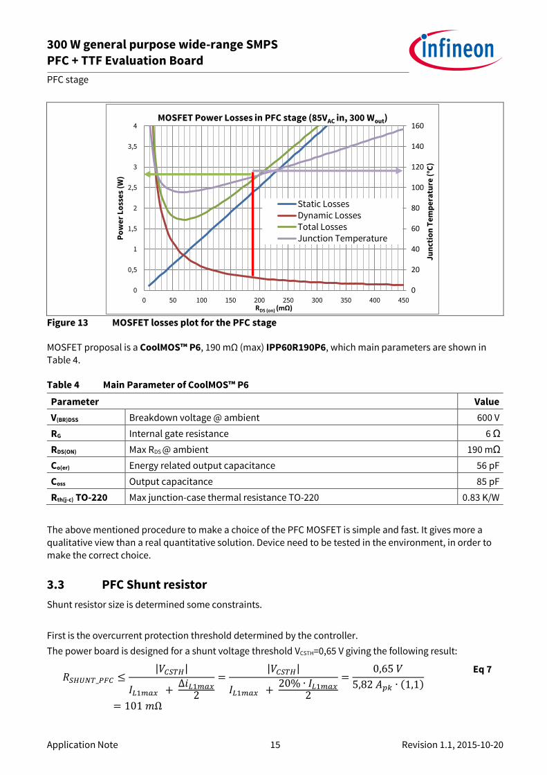
Figure 13 (described in Chapter 10: Appendix B), represents plots of losses in the power MOSFET as well as
junction temperature. Chart shows total power losses are about 3 W with RDS(on) Q1 = 190 mΩ. Junction
temperature rise will increase the effective RDS(on), by a factor of about 1.5, reaching higher junction
temperature close to 140°C if steady state load is considered.
300 W general purpose wide-range SMPS PFC + TTF Evaluation Board
PFC stage
Application Note 15 Revision 1.1, 2015-10-20
Figure 13 MOSFET losses plot for the PFC stage
MOSFET proposal is a CoolMOS™ P6, 190 mΩ (max) IPP60R190P6, which main parameters are shown in Table 4.
Table 4 Main Parameter of CoolMOS™ P6
Parameter Value
V(BR)DSS Breakdown voltage @ ambient 600 V
RG Internal gate resistance 6 Ω
RDS(ON) Max RDS @ ambient 190 mΩ
Co(er) Energy related output capacitance 56 pF
Coss Output capacitance 85 pF
Rth(j-c) TO-220 Max junction-case thermal resistance TO-220 0.83 K/W
The above mentioned procedure to make a choice of the PFC MOSFET is simple and fast. It gives more a qualitative view than a real quantitative solution. Device need to be tested in the environment, in order to make the correct choice.
3.3 PFC Shunt resistor
Shunt resistor size is determined some constraints.
First is the overcurrent protection threshold determined by the controller.
The power board is designed for a shunt voltage threshold VCSTH=0,65 V giving the following result:
𝑅𝑆𝐻𝑈𝑁𝑇_𝑃𝐹𝐶 ≤|𝑉𝐶𝑆𝑇𝐻|
𝐼𝐿1𝑚𝑎𝑥 + ∆𝑖𝐿1𝑚𝑎𝑥
2
=|𝑉𝐶𝑆𝑇𝐻|
𝐼𝐿1𝑚𝑎𝑥 + 20% ∙ 𝐼𝐿1𝑚𝑎𝑥
2
=0,65 𝑉
5,82 𝐴𝑝𝑘 ∙ (1,1)
= 101 𝑚Ω
Eq 7
0
20
40
60
80
100
120
140
160
0
0,5
1
1,5
2
2,5
3
3,5
4
0 50 100 150 200 250 300 350 400 450
Ju
nct
ion
Te
mp
era
ture
(°C
)
Po
we
r L
oss
es
(W)
RDS (on) (mΩ)
MOSFET Power Losses in PFC stage (85VAC in, 300 Wout)
Static LossesDynamic LossesTotal LossesJunction Temperature

300 W general purpose wide-range SMPS PFC + TTF Evaluation Board
PFC stage
Application Note 16 Revision 1.1, 2015-10-20
A second point to keep in mind is the power dissipation:
𝑃𝑆𝐻𝑈𝑁𝑇_𝑃𝐹𝐶 = |𝑉𝐶𝑆𝑇𝐻| ∙ 𝐼𝐷(𝑟𝑚𝑠)𝑄1 = 0,65 ∙ 3.55 𝐴 = 2,3 𝑊
Eq 8
In order to fulfill both requirements, 3 shunt resistors of 330 mΩ in parallel have been used. The choice is on
1 W SMD resistors, type “2512” resistors to keep also low the stray inductance, which would cause spikes on the sensed voltage.
3.4 PFC diode design
PFC diode proposal is also important, and need some considerations. In particular, diode recovery in hard
switching applications is an important parameter.
This design is a CCM PFC design, where diode recovery happens at almost every commutation period when in high load conditions.
Recovery generates high current spikes that create
High frequency commutation noise that generates conducted common mode noise at mid/hi- frequency
High amplitude spikes in the MOSFET channel during turn-on. Spikes have to be filtered by a leading
edge blanking filter from the controller (usually always present). This current creates additional losses in the MOSFET, flowing through the channel at turn-on
The output power of the proposed converter is such that a small SiC diode can be used. Here we have chosen a 3 A device in 5th Generation thinQ!™ technology: IDH03G65C5.
Table 5 IDH03G65C5 summary of parameters. Please refer to component datasheet for details
Parameter Value
VRRM Repetitive peak reverse voltage 650 V
IF Continuous forward current 3 A
IF(max) Non-repetitive peak forward current 178 A
VF Diode forward voltage @ ambient 1.5 VpF
QC Total capacitive charge 5 nC
Rth(j-c) TO-220 Max junction-case thermal resistance TO-220 3.6 K/W
3.5 PFC capacitor design
PFC bulk capacitor is designed according to required hold-up time. The requirement is usually to keep a minimum voltage of 340 V for 20 ms line drop at maximum output power.
Assuming a constant discharge of the bulk capacitor, Eq 9 can be applied to calculate the minimum Capacitance required.
1
2𝐶𝑏𝑢𝑙𝑘(𝑉𝑏𝑢𝑠
2 − 𝑉𝑏𝑢𝑠,min2 ) ≥ 𝑃𝑜𝑢𝑡,𝑚𝑎𝑥 ∙ ∆𝑡 → 𝐶𝑏𝑢𝑙𝑘 ≥
300 𝑊 ∙ 20 𝑚𝑠
3802 𝑉 − 3402 𝑉= 208 𝑢𝐹
Eq 9
Bus capacitor is a 220 µF, 450 V electrolytic, with additional 100 nF high frequency film cap bypass.
300 W general purpose wide-range SMPS PFC + TTF Evaluation Board
TTF Stage
Application Note 17 Revision 1.1, 2015-10-20
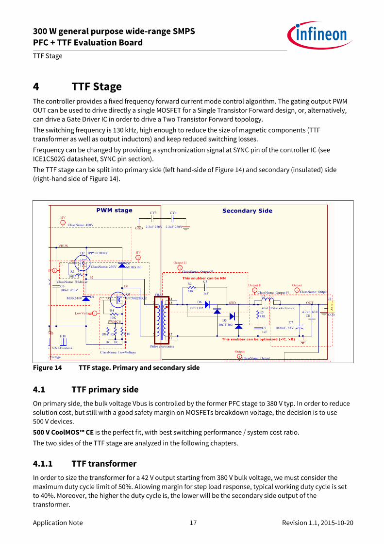
4 TTF Stage The controller provides a fixed frequency forward current mode control algorithm. The gating output PWM
OUT can be used to drive directly a single MOSFET for a Single Transistor Forward design, or, alternatively, can drive a Gate Driver IC in order to drive a Two Transistor Forward topology.
The switching frequency is 130 kHz, high enough to reduce the size of magnetic components (TTF transformer as well as output inductors) and keep reduced switching losses.
Frequency can be changed by providing a synchronization signal at SYNC pin of the controller IC (see ICE1CS02G datasheet, SYNC pin section).
The TTF stage can be split into primary side (left hand-side of Figure 14) and secondary (insulated) side
(right-hand side of Figure 14).
Figure 14 TTF stage. Primary and secondary side
4.1 TTF primary side
On primary side, the bulk voltage Vbus is controlled by the former PFC stage to 380 V typ. In order to reduce
solution cost, but still with a good safety margin on MOSFETs breakdown voltage, the decision is to use 500 V devices.
500 V CoolMOS™ CE is the perfect fit, with best switching performance / system cost ratio.
The two sides of the TTF stage are analyzed in the following chapters.
4.1.1 TTF transformer
In order to size the transformer for a 42 V output starting from 380 V bulk voltage, we must consider the
maximum duty cycle limit of 50%. Allowing margin for step load response, typical working duty cycle is set to 40%. Moreover, the higher the duty cycle is, the lower will be the secondary side output of the transformer.

300 W general purpose wide-range SMPS PFC + TTF Evaluation Board
TTF Stage
Application Note 18 Revision 1.1, 2015-10-20
Ideally Vout and Vbus are linked by the following Eq 10.
𝑉𝑜𝑢𝑡
𝑉𝑏𝑢𝑠=
𝑁𝑠𝑒𝑐
𝑁𝑝𝑟𝑖𝑚∙ 𝐷𝑝𝑤𝑚
Eq 10
𝑁𝑠𝑒𝑐
𝑁𝑝𝑟𝑖𝑚=
𝑉𝑜𝑢𝑡
𝑉𝑏𝑢𝑠 ∙ 𝐷𝑃𝑊𝑀=
42 𝑉
380𝑉 ∙ 0.4=
1
3.62
Eq 11
Transformer primary inductance LTRA1 value has been set in order to ensure enough magnetizing current to properly set / reset the core. During the primary-side turn-on period, the magnetizing inductance is charged by a current IMAG which must be reset during the turn-off time. IMAG peak is set to about 400 mA in
order to keep small the recirculation diodes and limit the recirculation current which creates EMI current loops. 1 A fast-diodes D3 and D4 are used.
𝐿𝑇𝑅𝐴1 ≥ 𝑉𝐵𝑈𝑆
𝐼𝑀𝐴𝐺∙
𝐷𝑃𝑊𝑀
𝑓𝑠𝑤(𝑃𝑊𝑀)=
380 𝑉
400 𝑚𝐴∙
0,4
130 𝑘𝐻𝑧= 2,9 𝑚𝐻
Eq 12
Specification from magnetics manufacturer follows on Figure 15 where primary side inductance is higher and allows lower values of IMAG.
The choice is on Pulse Electronics (PH9326NL), which is a transformer without shield. Shield design for the transformer was not studied in details, but it might be necessary in certain cases.
Figure 15 TTF transformer specification 42 V, from Pulse Electronics
Primary side current derives from choice of secondary side current ripple.
The choice is done in such a way that at 15% load the output stage is in Boundary Condition Mode, which means the ripple current touches zero at the end of each cycle. Then, in order to have an output current
ripple of about 30% of the maximum load current, ripple current is calculated from Eq 14:
𝐼𝑜(𝑎𝑣𝑔) =𝑃𝑜𝑢𝑡
𝑉𝑜𝑢𝑡=
300 𝑊
42 𝑉= 7.15 𝐴 Eq 13
𝐼𝑟𝑖𝑝𝑝𝑙𝑒 = 30% ∙ 𝐼𝑜(𝑎𝑣𝑔) = 30% ∙ 7.15 𝐴 = 2.2 𝐴 Eq 14

300 W general purpose wide-range SMPS PFC + TTF Evaluation Board
TTF Stage
Application Note 19 Revision 1.1, 2015-10-20
4.1.2 TTF Primary side MOSFETs
To size the primary side components, the primary side currents have to be calculated. The following equations show how to calculate the most important currents of the primary side used to size the switches.
𝐼𝑀𝐴𝐺 =𝑉𝐵𝑈𝑆
𝐿𝑇𝑅𝐴1∙
𝐷𝑃𝑊𝑀
𝑓𝑠𝑤(𝑃𝑊𝑀)=
380 𝑉
3,5 𝑚𝐻∙
0,4
130 𝑘𝐻𝑧= 334 𝑚𝐴
Magnetizing current
Eq 15
𝐼𝑀𝑂𝑆(sec _𝑚𝑖𝑛) = 𝐼o(𝑚𝑖𝑛) ∙𝑁𝑠𝑒𝑐
𝑁𝑝𝑟𝑖𝑚= 6.05 𝐴 ∙
1
3.59= 1.68 𝐴
𝐼𝑀𝑂𝑆(sec _𝑚𝑎𝑥) = 𝐼o(𝑚𝑎𝑥) ∙𝑁𝑠𝑒𝑐
𝑁𝑝𝑟𝑖𝑚= 8.25 𝐴 ∙
1
3.59= 2.3 𝐴
Load current seen by
primary side
Eq 16
𝐼𝑀𝑂𝑆(𝑚𝑎𝑥) = 𝐼MOS(sec _𝑚𝑎𝑥) + 𝐼𝑀𝐴𝐺 = 2.63 𝐴 Primary MOS peak current
Eq 17
𝐼𝑀𝑂𝑆(𝑟𝑚𝑠) =
=√(𝐼𝑀𝑂𝑆(max )
2 + (𝐼𝑀𝑂𝑆(sec _𝑚𝑖𝑛) + 𝐼𝑀𝐴𝐺)2
+ 𝐼𝑀𝑂𝑆(max) ∙ (𝐼𝑀𝑂𝑆(sec _𝑚𝑖𝑛) + 𝐼𝑀𝐴𝐺))
3= 2 𝐴
MOS rms current
Eq 18
The following Figure 16 shows the naming conventions used.
IMAG
IMOS(sec_min)
IMOS(sec_max)
IMOSmax
I o(r
ipp
le)
Io(max)
T
Io(min)
Ton=DPWMT
Io(avg)
Figure 16 Current shapes on primary MOSFET (IMOS) and output inductor (Io)
As well as for the PFC, for the TTF stage, MOSFETs Q2 and Q3 work in hard switching, and then selection
criteria are the same as in the PFC stage: low Qg, Coss, Eon, and Eoff are required to decrease switching losses. We are going to use the same graphical procedure as or the PFC.
300 W general purpose wide-range SMPS PFC + TTF Evaluation Board
TTF Stage
Application Note 20 Revision 1.1, 2015-10-20
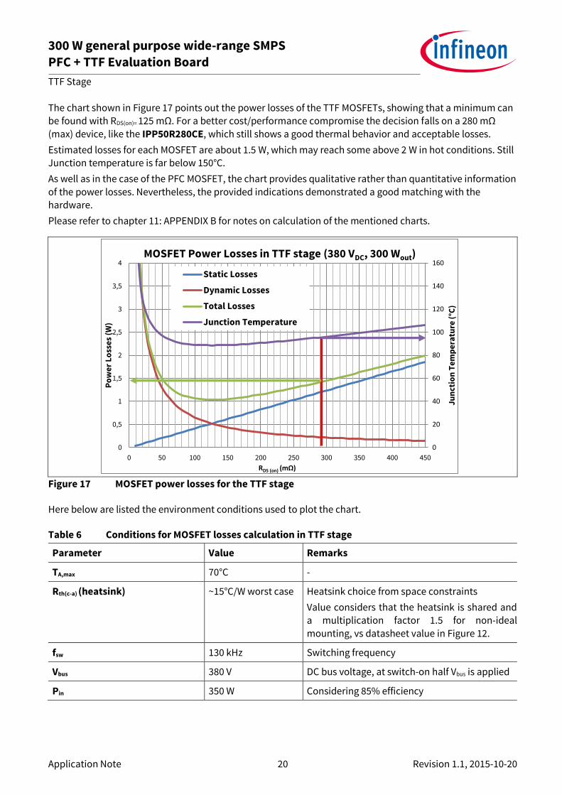
The chart shown in Figure 17 points out the power losses of the TTF MOSFETs, showing that a minimum can be found with RDS(on)= 125 mΩ. For a better cost/performance compromise the decision falls on a 280 mΩ
(max) device, like the IPP50R280CE, which still shows a good thermal behavior and acceptable losses.
Estimated losses for each MOSFET are about 1.5 W, which may reach some above 2 W in hot conditions. Still Junction temperature is far below 150°C.
As well as in the case of the PFC MOSFET, the chart provides qualitative rather than quantitative information
of the power losses. Nevertheless, the provided indications demonstrated a good matching with the hardware.
Please refer to chapter 11: APPENDIX B for notes on calculation of the mentioned charts.
Figure 17 MOSFET power losses for the TTF stage
Here below are listed the environment conditions used to plot the chart.
Table 6 Conditions for MOSFET losses calculation in TTF stage
Parameter Value Remarks
TA,max 70°C -
Rth(c-a) (heatsink) ~15°C/W worst case Heatsink choice from space constraints
Value considers that the heatsink is shared and a multiplication factor 1.5 for non-ideal
mounting, vs datasheet value in Figure 12.
fsw 130 kHz Switching frequency
Vbus 380 V DC bus voltage, at switch-on half Vbus is applied
Pin 350 W Considering 85% efficiency
0
20
40
60
80
100
120
140
160
0
0,5
1
1,5
2
2,5
3
3,5
4
0 50 100 150 200 250 300 350 400 450J
un
ctio
n T
em
pe
ratu
re (
°C)
Po
we
r L
oss
es
(W)
RDS (on) (mΩ)
MOSFET Power Losses in TTF stage (380 VDC, 300 Wout)
Static Losses
Dynamic Losses
Total Losses
Junction Temperature

300 W general purpose wide-range SMPS PFC + TTF Evaluation Board
TTF Stage
Application Note 21 Revision 1.1, 2015-10-20
MOSFET proposal is a CoolMOS™ CE, 280 mΩ (max) IPP50R280CE, which main parameters are shown in Table 7.
Table 7 IPP50R280CE summary of parameters. Please refer to component datasheet for details
Parameter Value
V(BR)DSS Breakdown voltage @ ambient 500 V
RG Internal gate resistance 3 Ω
RDS(ON) Max RDS @ ambient 280 mΩ
Co(er) Energy related output capacitance 40 pF
Coss Output capacitance 49 pF
Rth(j-c) TO-220 Max junction-case thermal resistance TO-220 1.36 K/W
A note shall be pointed out for the choice of the freewheeling diodes D3 and D4.
Note: Even though the magnetization current IMAG they bring may appear small, and the switch off smoothly
(ZCS) it is important that the choice falls on fast reverse recovery diodes. D3 and D4 are MURS160.
Note: Layout design of TTF is not easy, and demagnetization path is usually longer than main path. This path
is partially responsible for emissions and must be carefully studied, starting for the device choice. Layout of the board described in this application note, is unfortunately not perfectly optimized in this path.
4.1.3 TTF shunt resistor
Same procedure as for the PFC stage has been taken for the TTF shunt resistor choice.
The power board is designed for a shunt voltage threshold Vcsth=1 V giving the following result:
𝑅𝑆𝐻𝑈𝑁𝑇_𝑇𝑇𝐹 ≤|𝑉𝐶𝑆𝑇𝐻|
𝐼𝑀𝑂𝑆(𝑚𝑎𝑥)=
1 𝑉
2,63 𝐴𝑝𝑘= 380 𝑚𝑂ℎ𝑚
Eq 19
A second point to keep in mind is the power dissipation:
𝑃𝑆𝐻𝑈𝑁𝑇_𝑇𝑇𝐹 = |𝑉𝐶𝑆𝑇𝐻| ∙ 𝐼𝑀𝑂𝑆(𝑟𝑚𝑠) = 1 𝑉 ∙ 2𝐴 = 2 𝑊
Eq 20
In order to fulfill both requirements, and to keep some flexibility, 3 shunt resistors of 1 Ω in parallel have been used. The choice is on 1 W SMD resistors, type “2512” to keep also low the stray inductance, which
would cause spikes on the sensed voltage.
4.1.4 MOSFET gate driving
The gate driving of the TTF power MOSFETs is done using an Infineon EiceDRIVER™ gate driver IC 2EDL05I06BF. The gate driver IC is a non-interlocking driver, so that high side and low side can be turned-on simultaneously, which is necessary in a TTF topology.

300 W general purpose wide-range SMPS PFC + TTF Evaluation Board
TTF Stage
Application Note 22 Revision 1.1, 2015-10-20
The gate driving section is shown in Figure 18, where input of the IC is “PWMOUT” (which comes from the control board) and G3, G2, S2 represent respectively the low-side MOSFET gate and the high-side MOSFET
gate and source.
D11 and D12 are optional turn-off paths and can be removed. There is no Miller induced turn-off effect in TTF, since both MOSFETs are turned on simultaneously. Turn-on can be soft, since the topology allows zero load current switching and only capacitive spike take place at turn-on.
Trimming on gate driving resistance are mainly related to a compromise between switching behavior and high frequency oscillations that may be induced by layout problems.
Figure 18 Gate driver IC schematic
The use of a gate driver versus a pulse transformer (widely used in this topology), is the capability to control and keep well above the threshold voltage the gate of the MOSFETs, allowing a safe driving in all supply
conditions.
Especially in case of failures or difficult layout situations, the gate driver IC solves grounding problems and
helps placing the drive buffers closer to the MOSFETs to be controlled. In this power supply the choice of a gate driver IC solution pairs with the use of a controller daughterboard, where there may be different kind of
controllers.
Moreover it avoids the typical effect of pulse transformers, where there can be an effect of offset shifting of
the gate driving signals, which is dependent on duty cycle as shown in the following picture.
Pulse transformer
Pulse transformer Gate driver
Figure 19 Typical offset shifting when using pulse transformer
Please note that the bootstrap supply cannot be applied to TTF topology to supply the hi-side buffer. Auxiliary power supply is necessary.

300 W general purpose wide-range SMPS PFC + TTF Evaluation Board
TTF Stage
Application Note 23 Revision 1.1, 2015-10-20
4.2 TTF secondary side
Secondary side schematic is shown in Figure 20.
Figure 20 TTF secondary side schematic
4.2.1 TTF rectifier diodes
Secondary output voltage VSEC is then rectified by Schottky Barrier Rectifier D5 and D6 (30CTH02PBF): diodes in common cathode configuration, having then a rectifier (in series with the transformer) and a freewheeling
path. Synchronous rectification (SR) could also be available with two MOSFETs for power loss reduction with an external driver.
Two snubber protections are also present (R2 - C5 and R5 - C9), in order to reduce inductor L3 overvoltage
and dump the oscillations. R2 – C5 in particular are redundant and can be used for testing.
RC pole should be located in the 10 ... 50 MHz range, and have to be trimmed as a function of snubbering effect, by watching at the waveforms across the diodes.
Diodes theoretical reverse voltage VSRD is derived from the following Eq 21:
𝑉𝑆𝑅𝐷𝑚𝑎𝑥 =𝑉𝑜𝑢𝑡
𝐷𝑃𝑊𝑀=
42 𝑉
0.4= 105 𝑉 Purely theoretical value Eq 21
But the equation doesn’t take into account the spikes and overshoots due to stray components.
The board is equipped with 200 V diodes, and the measured peak voltage at maximum load gets repetitively
voltages up to 160 V for few nanoseconds, with the proposed snubbers.
Output diodes are one of the main source of losses and shottky diodes are necessary. A second and equally
important characteristic of the diode is the switching behavior, which has to be ultrafast and smooth. Several kind of diodes has to be proven before a final choice, because the switching behavior strongly influences the primary side, through the transformer and the conducted and emitted noise.
Rectifier diode losses are due to secondary current ISEC (avg). For rough estimation of power losses for the
secondary side, it might be considered the following chart and calculation at peak output power:

300 W general purpose wide-range SMPS PFC + TTF Evaluation Board
TTF Stage
Application Note 24 Revision 1.1, 2015-10-20
Io(MAX)
VSRD(ideal)
T
Ton=DPWMT
Io(MIN)
IDR IDF
VOUT=42V
I o(r
ipp
le)
DR
DF
VOUT
VSRD
Figure 21 Output ideal waveforms and circuit
𝑃𝐷𝑅 = 𝑉𝐹 ∙ 𝐼𝐷𝑅(𝑎𝑣𝑔) = 0.65 𝑉 ∙ √0.4 ∙ (6.052 + 6.05 ∙ 8.25 + 8.252)
3𝐴 = 0.65 𝑉 ∙ 4.54 𝐴
= 2.95 𝑊
Eq 22
𝑃𝐷𝐹 = 𝑉𝐹 ∙ 𝐼𝐷𝐹(𝑎𝑣𝑔) = 0.65 𝑉 ∙ √0.6 ∙ (6.052 + 6.05 ∙ 8.25 + 8.252)
3𝐴 = 0.65 𝑉 ∙ 5.56 𝐴
= 3.61 𝑊
Eq 23
Calculation of diodes average currents in Eq 22 and Eq 23 follow examples in Chapter 9: APPENDIX A.
The calculation takes into account only the conduction losses.
A very rough estimation of diode switching losses can be done considering the datasheet value of Qrr=120 nC
@125°C vs reverse commutated voltage VSRD=105 V at fsw=130 kHz, which gives about PDSW=1,64 W additional per diode.
The power board hosts space for mounting two pairs of common cathode diodes.
In order to allow power dissipation for the diodes in continuous load conditions can be done the following
estimation for the required heatsink Rthja =Rthjc+Rthca:
𝑅𝑇𝐻𝑗𝑎 <𝑇𝑗 − 𝑇𝑎
𝑃𝐷=
𝑇𝑗 − 𝑇𝑎
𝑃𝐷𝑅 + 𝑃𝐷𝐹 + 2 ∙ 𝑃𝐷𝑆𝑊=
150°𝐶 − 70°𝐶
2.95 𝑊 + 3.61 𝑊 + 2 ∙ 1.64 𝑊= 8°𝐶/𝑊
Eq 24

300 W general purpose wide-range SMPS PFC + TTF Evaluation Board
TTF Stage
Application Note 25 Revision 1.1, 2015-10-20
4.2.2 TTF output passives
Design for LC output inductor and capacitor tank starts from the assumption that the entire ripple component in inductor current ΔIL3 flows through C7, while its average component flows through the load. During off-time toff (PWM) = (1 – DPWM) ∙ Tsw (PWM), inductor ripple current is:
∆𝐼𝐿3𝑚𝑎𝑥 =𝑉𝑜𝑢𝑡
𝐿3∙ (1 − 𝐷𝑃𝑊𝑀) ∙ 𝑇𝑠𝑤 =
𝑉𝑜𝑢𝑡
𝐿3∙
(1 − 𝐷𝑃𝑊𝑀)
𝑓𝑠𝑤(𝑃𝑊𝑀)
Eq 25
and the output inductor is calculated as follows:
𝐿3 =𝑉𝑜𝑢𝑡
∆𝐼𝐿3𝑚𝑎𝑥∙
(1 − 𝐷𝑃𝑊𝑀)
𝑓𝑠𝑤(𝑃𝑊𝑀)=
42 𝑉
2.2 𝐴∙
(1 − 0.4)
130 𝑘𝐻𝑧= 88 𝜇𝐻
Eq 26
The output inductor was manufactured by Pulse Electronics (PH9327NL), as well. The core is toroidal and specification from manufacturer follows in Figure 22:
Figure 22 Output inductor specification, from Pulse Electronics
To find an indication about sizing the output capacitor, the output voltage ripple must be fixed. Let’s start fixing ΔVout = 0.01%·Vout = 40 mV. Then let’s consider that the inductor current charges and discharges by ±ΔQ the output capacitor, so that the output ripple can be calculated as follows:
∆𝑉𝑜𝑢𝑡 =∆𝑄
𝐶=
1
𝐶∙ (
∆𝐼𝐿3 ∙ 𝑇𝑠𝑤(𝑃𝑊𝑀)
8) Eq 27
Replacing ΔIL3 from Eq 25 the relative ripple can be obtained as:
∆𝑉𝑂𝑈𝑇
𝑉𝑂𝑈𝑇=
1
8∙
1 − 𝐷𝑃𝑊𝑀
𝐿𝐶 ∙ 𝑓𝑠𝑤 (𝑃𝑊𝑀)2 ≤ 0.01%
Eq 28
And the output capacitor:
𝐶 ≥1
8∙
1 − 𝐷𝑃𝑊𝑀
𝐿 ∙ 𝑓𝑠𝑤 (𝑃𝑊𝑀)2 ∙
1
0.01%=
1
8∙
1 − 0.4
80 𝜇𝐻 ∙ (130 𝑘𝐻𝑧)2∙
1
0.01%= 550 𝜇𝐹
Eq 29
This value may be able to keep the ripple, but the ESR of the capacitor plays and important role. During load jumps, the major drops and jumps are due to stray inductances and resistive behavior.
Best choice may is a parallel of smaller electrolytic capacitors and a good low ESR cap.
Our board as a general purpose demonstrator is equipped with a single 1000 µF capacitor and a small high frequency ceramic capacitor.

300 W general purpose wide-range SMPS PFC + TTF Evaluation Board
TTF Stage
Application Note 26 Revision 1.1, 2015-10-20
An additional LC output filter is necessary for EMI/EMC compliance, when the output is connected to a load with cables.
Purpose of this work is to provide a supply for different application, but in particular in conjunction with an on-board motor drive system. For this reason, the LC filter has not been provided.
4.2.3 TTF feedback
The loop feedback is using a standard approach with TL431 and opto-coupler circuit, as shown in.
Figure 23 TTF voltage feedback
In particular output voltage can be scaled as follows:
𝑉𝑜𝑢𝑡 = 2.5 𝑉 ∙ [1 +(𝑅21 + 𝑅22)
𝑅33] + 𝑉𝐷𝑍3 = 42 𝑉
Eq 30
Note on DZ3:
TL431A absolute maximum voltage is 37 V and current is 150 mA. DZ3 is used to avoid voltage/current stress on the regulator.
If different output voltage is desired it can be either chosen a different zener voltage for DZ3 according to Table 8, or DZ3 can be replaced with a 0 Ohm resistor and it can be changed the resistor divider.
Attention:
The power board output stage is designed for 42 V, 300 W peak power.
The board can work for lower output voltages without changing the main components, but:
Changing the output voltage requires reducing the output current. Approximate output power is indicated in Table 7.
When keeping the same output power, output diodes, output inductor and transformer MUST be redesigned due to higher currents.
300 W general purpose wide-range SMPS PFC + TTF Evaluation Board
TTF Stage
Application Note 27 Revision 1.1, 2015-10-20
Table 8 Output voltage and power scaling
Desired output voltage Action Approximate Max
output power (according to 50% duty)
Critical points and
optimization
24 V Replace DZ3 with 0Ohm
resistor
150 W Output diodes cooling
Un-efficient usage of
trafo
36 V DZ3=12 Vz 220 W Output diodes cooling
42 V DZ3=18 Vz 300 W
48 V DZ3=24 Vz 300 W
Following the above mentioned table, primary side relaxes to lower power consumption. The main limit is the power dissipation of the output diodes, the current of which is inverse-proportionally increasing as output voltage decrease.
The same transformer can be used for the indicated output voltages, since the controller will act on duty cycle to provide the desired output, BUT it will work with higher output voltages and peak currents than
needed. A correct transformer design would generate lower output voltage at rectification diodes, which allows the choice of better rectifiers with lower voltage and current peaks.
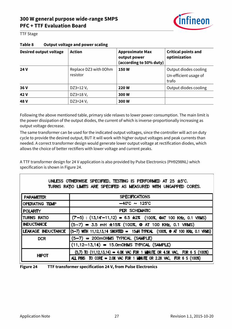
A TTF transformer design for 24 V application is also provided by Pulse Electronics (PH9298NL) which
specification is shown in Figure 24.
Figure 24 TTF transformer specification 24 V, from Pulse Electronics

300 W general purpose wide-range SMPS PFC + TTF Evaluation Board
Auxiliary power supply
Application Note 28 Revision 1.1, 2015-10-20
5 Auxiliary power supply A flyback circuit has been implemented in order to provide forward converter start-up and supply. Its input
is the bus voltage VBUS, and provides a ground referenced VCC = 15 VDC for the controller board, as well as an insulated VCC = 15 VDC for the high side gate driving for the TTF.
The Auxiliary power supply is designed to provide a max of about 3 W, and the schematic is shown below.
Figure 25 ICE CoolSET™ Auxiliary power supply schematic
The schematic provides the possibility to use both a quasi-resonant flyback as well as a fixed frequency
flyback. The choice for this design is the ICE3AR10080JZ, which is a 10 Ω, 100 kHz CoolSET™ controller with integrated 800 V MOSFET, in DIP7 package.
The switching frequency of 100 kHz allows the use of a small transformer, with DIP8 footprint. The transformer was designed to be with functional insulation, since it doesn’t supply secondary side circuits.
The transformer was provided by Pulse Electronics (PH9323NL) with the attached specifications:
Figure 26 Flyback transformer specification, from Pulse Electronics

300 W general purpose wide-range SMPS PFC + TTF Evaluation Board
Auxiliary power supply
Application Note 29 Revision 1.1, 2015-10-20
Design guidelines for the flyback design can be found in Infineon website, at CoolSET™ fixed frequency controller page, searching for ICE3AR10080JZ.
The auxiliary supply is taken from the bus voltage and start-up is guaranteed from 80 VAC input. As soon as the PFC starts working, the Bus voltage goes to 380 V.The auxiliary power supply works mainly in burst mode, which allows low power consumption and less emission.
The advantage of a flyback supply is the possibility to add windings and provide insulated supply voltage to the secondary side. This requires a different insulation for the transformer, but helps especially when a complete turn-off of the main power stage (PFC+TTF) is required by the secondary side controller, while the auxiliary works as a low consumption standby supply.
This Application Note does not implement the above mentioned proposal, which is anyway recommended
to achieve very low standby consumption and full control of the power stage from the secondary side.
The auxiliary flyback can be configured in a quasi-resonant configuration allowing to use the ICE2QR4765Z.
The list below shows the modifications on the power board, which are necessary to use one or the other solution.
Note: While the Fixed Frequency configuration has been tested and optimized, the Quasi-Resonant configuration is provided by theory and has not been tested.
Table 9 Fixed Frequency vs Quasi-Resonant Flyback component configuration
Component Fixed frequency flyback Quasi resonant flyback
Device ICE3AR10080JZ ICE2QR4780Z
R35 Mount Do Not Mount
R17 Do Not Mount Mount
C16 Do Not Mount Mount
R22 Mount Mount
300 W general purpose wide-range SMPS PFC + TTF Evaluation Board
Control card with ICE1CS02G
Application Note 30 Revision 1.1, 2015-10-20
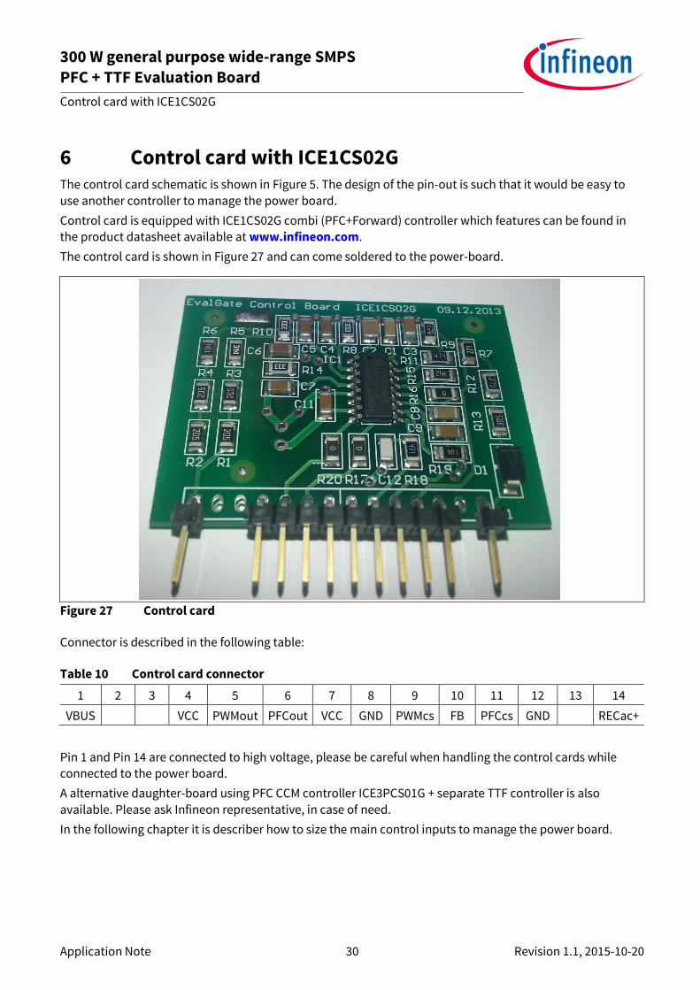
6 Control card with ICE1CS02G The control card schematic is shown in Figure 5. The design of the pin-out is such that it would be easy to
use another controller to manage the power board.
Control card is equipped with ICE1CS02G combi (PFC+Forward) controller which features can be found in the product datasheet available at www.infineon.com.
The control card is shown in Figure 27 and can come soldered to the power-board.
Figure 27 Control card
Connector is described in the following table:
Table 10 Control card connector
1 2 3 4 5 6 7 8 9 10 11 12 13 14
VBUS VCC PWMout PFCout VCC GND PWMcs FB PFCcs GND RECac+
Pin 1 and Pin 14 are connected to high voltage, please be careful when handling the control cards while connected to the power board.
A alternative daughter-board using PFC CCM controller ICE3PCS01G + separate TTF controller is also
available. Please ask Infineon representative, in case of need.
In the following chapter it is describer how to size the main control inputs to manage the power board.

300 W general purpose wide-range SMPS PFC + TTF Evaluation Board
Control card with ICE1CS02G
Application Note 31 Revision 1.1, 2015-10-20
6.1 PFC voltage and current loop
Pin 14: RECac+
Pins VINS (Input Voltage Sensing) and VINS HYS (Input Voltage Sensing Hysteresis) of the combi combi controller derive from RECac+ thorough a resistor divider. These controller pins sense, in fact, the rectified
AC main line signal RECAC+.
VINS senses the input mains voltage protecting the system from brown-out (BOP): brown-out happens when the input voltage VINRMS falls below the minimum designed input voltage (i.e. VINRMS < 85.0 VAC). Brown-out
protection avoids large currents flowing in the PFC stage in low-line voltage conditions. When input voltage is under minimum designed input voltage, i.e. VINRMS < 85.0 V, PFC gate signal is stopped and then resumed
with standard start-up procedure when proper AC input voltage is restored.
Maximum value of RECAC+ (~ √2 ∙ VINRMS) is hence detected by this pin and maintained by a capacitor: when
proper input voltage is applied (85 VAC ≤ VINRMS ≤ 265 VAC), stand-by mode is switched-off. Hysteresis pin (VIN
HYS) prevents the system to oscillate between normal and stand-by mode.
Pin 1: VBUS and Pin 6: PFC out
Here are connected the pins of PFC VSENSE (Bus Voltage Sense / Feedback) and PFC OVP (Overvoltage Sense Input). Output bus voltage VBUS is sensed via a resistive divider. PFC OUT is then enabled and PFC
duty cycle DPFC is gradually increased by soft-start until VBUS reaches the desired voltage, thus also enabling the PWM TTF controller section.
On the other hand, PFC OVP provides overvoltage protection by reducing or stopping the PFC duty cycle.
Pin 11: PFC CS
Associated to PFC CS is the controller pin PFC ISENSE (Current Sense Input). This input senses the PFC
MOSFET current by resistance RSHUNT_PFC. RSHUNT_PFC has been designed on the ICE1CS02 PFC peak
current limitation (PCL, VPCL) protection: when the PFC ISENSE signal reaches the PCL threshold, PFC gate
switching will shut down.
Leading Edge Blanking time (220 ns, LEB) is integrated in order to prevent current limit protection from distortions caused by edge spikes; moreover; an additional filtering can be set by adding a capacitor
between PFC ISENSE and ground. According to IC datasheet, PCL threshold for PFC stage is about –0.60 V.
Check for shunt resistor sizing in chapter 3.3 (“PFC Shunt resistor”) on page 15.
Pin 10: FB and Pin 5: PWM OUT
Pin FB is the TTF stage voltage feedback, associated with Pin 12 – PWM FB (PWM Feedback): output voltage
VOUT is sensed by PWM FB via opto- opto-coupler. PWM OUT (controller pin 8) regulates duty cycle of the TTF converter in order to achieve a regulated output voltage VOUT. Feedback loop and controller are
electrically isolated: error voltage signal is provided to the controller by a 1:1 current from opto-coupler and compared to the internal reference voltage (VREF=5 V). PWM OUT is provided to Q2 and Q3 by a gate driver IC 2EDL05I06BF which is described in chapter 4 (“TTF gate driver 2EDL05I06BF”) on page 6.
Pin 9: PWM CS:
PWM CS provides the TTF current sense information to the controller IC PWM CS pin (PWM Current Sense). RSHUNT_PWM value has been designed to provide peak current limitation (Vcsth) via ICE1CS02 PWM
protection. According to IC datasheet, PWM threshold for PFC stage Vcsth = 1.00 V. Shunt sizing is explained in chapter 4.1.3 (“TTF shunt resistor”) on page 21.

300 W general purpose wide-range SMPS PFC + TTF Evaluation Board
Control card with ICE1CS02G
Application Note 32 Revision 1.1, 2015-10-20
In case noise filtering is necessary, it can be set by adding a RC-network (R18 and C12); in this board, τ = R18∙C12 ~ 300 ns.
When the PWM ISENSE signal at pin 9 reaches the limit threshold for a period set externally through pin 11 (PWM Pre-Short), the TTF control is switched off. Timing of Preshort is set to about ~10 ms with C9 = 100 nF.
There is no restart of the system, unless the input line is cycled. Please refer to ICE1CS02G datasheet for details.
300 W general purpose wide-range SMPS PFC + TTF Evaluation Board
Converter test results
Application Note 33 Revision 1.1, 2015-10-20
7 Converter test results Power supply test results will be briefly shown in this chapter. Tests were performed at ambient
temperature with various loads. Collection of data is done on a single prototype (no statistical data was performed).
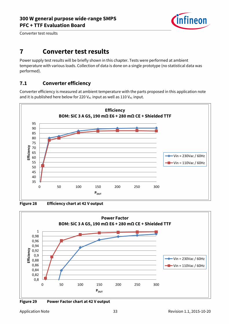
7.1 Converter efficiency
Converter efficiency is measured at ambient temperature with the parts proposed in this application note and it is published here below for 220 VAC input as well as 110 VAC input.
Figure 28 Efficiency chart at 42 V output
Figure 29 Power Factor chart at 42 V output
35
40
45
50
55
60
65
70
75
80
85
90
95
0 50 100 150 200 250 300
Effi
cie
ncy
POUT
Efficiency
BOM: SiC 3 A G5, 190 mΩ E6 + 280 mΩ CE + Shielded TTF
Vin = 230Vac / 60Hz
Vin = 110Vac / 60Hz
0,8
0,82
0,84
0,86
0,88
0,9
0,92
0,94
0,96
0,98
1
0 50 100 150 200 250 300
Effi
cie
ncy
POUT
Power Factor
BOM: SiC 3 A G5, 190 mΩ E6 + 280 mΩ CE + Shielded TTF
Vin = 230Vac / 60Hz
Vin = 110Vac / 60Hz
300 W general purpose wide-range SMPS PFC + TTF Evaluation Board
Converter test results
Application Note 34 Revision 1.1, 2015-10-20
7.2 Converter waveforms
7.2.1 PFC plots
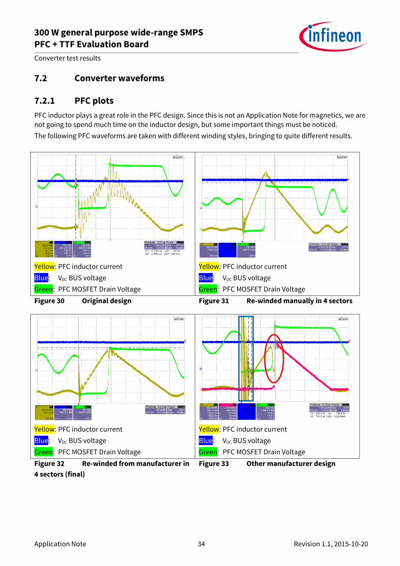
PFC inductor plays a great role in the PFC design. Since this is not an Application Note for magnetics, we are
not going to spend much time on the inductor design, but some important things must be noticed.
The following PFC waveforms are taken with different winding styles, bringing to quite different results.
Yellow: PFC inductor current
Blue: VDC BUS voltage
Green: PFC MOSFET Drain Voltage
Yellow: PFC inductor current
Blue: VDC BUS voltage
Green: PFC MOSFET Drain Voltage
Figure 30 Original design Figure 31 Re-winded manually in 4 sectors
Yellow: PFC inductor current
Blue: VDC BUS voltage
Green: PFC MOSFET Drain Voltage
Yellow: PFC inductor current
Blue: VDC BUS voltage
Green: PFC MOSFET Drain Voltage
Figure 32 Re-winded from manufacturer in
4 sectors (final)
Figure 33 Other manufacturer design

300 W general purpose wide-range SMPS PFC + TTF Evaluation Board
Converter test results
Application Note 35 Revision 1.1, 2015-10-20
Waveform explanation follows:
Figure 30: Original design Strong inter-winding coupling generate oscillations in the 10 MHz range (superimposed to yellow trace),
clearly visible in EMC test. Beginning and end of winding are superimposed in large part of the toroidal core.
Figure 31: Re-winded manually in 4 sectors
Manual winding didn’t allow same number of turns to test the absence of inter-winding coupling.
Much less coupling reduces drastically oscillations, which eventually shifted to very high frequency and
lower amplitude. Space is left intentionally between beginning and end of winding to reduce the capacitive
coupling between the physical leads.
Figure 32: Re-winded from manufacturer in 4 sectors (final)
Automatic winding with required inductance value in 4 sectors reduced greatly the inter-winding coupling, with a visible effect of oscillation reduction. Still some high frequency oscillations are present.
Figure 33: Other manufacturer design
Another manufacturer design has been tested, which is shown here to provide different scenarios.
Capacitive coupling between beginning and end of winding is clearly visible at current peak in the big dip
circled in red.
Very high frequency oscillations at MOSFET turn-on are produced instead by the cross-winding coupling,
which in this design is extended along the toroidal shape (blue square).
(Purple trace is PFC diode current, superimposed to inductor current)
Following plots are taken at 85 VAC input. Please note that the horizontal scales may change!
Figure 34 PFC 85 VAC, 5 Wout
Inductor current
Q1 VDS voltage Vrec_AC +

300 W general purpose wide-range SMPS PFC + TTF Evaluation Board
Converter test results
Application Note 36 Revision 1.1, 2015-10-20
Figure 35 PFC 85 VAC, 100 Wout
Figure 36 PFC 85 VAC, 300 Wout, PFC current limiting
At 300 W output with 85 VAC input, PFC stage is at current limit. Cycle-by-cycle limitation get triggered.
Peak voltage at MOSFET drain is less than 500 V.
Inductor current
Q1 VDS voltage Vrec_AC+
Inductor current
Q1 VDS voltage Vrec_AC+
300 W general purpose wide-range SMPS PFC + TTF Evaluation Board
Converter test results
Application Note 37 Revision 1.1, 2015-10-20
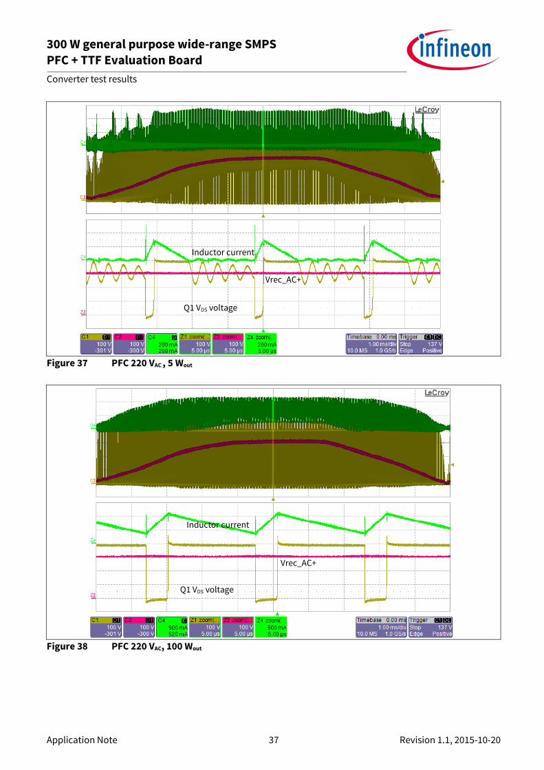
Figure 37 PFC 220 VAC , 5 Wout
Figure 38 PFC 220 VAC, 100 Wout
Inductor current
Q1 VDS voltage
Vrec_AC+
Inductor current
Q1 VDS voltage
Vrec_AC+
300 W general purpose wide-range SMPS PFC + TTF Evaluation Board
Converter test results
Application Note 38 Revision 1.1, 2015-10-20
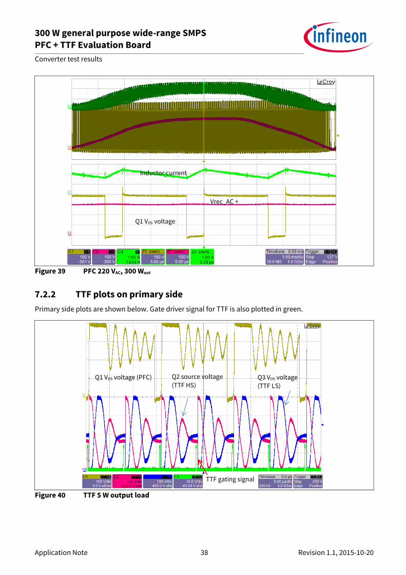
Figure 39 PFC 220 VAC, 300 Wout
7.2.2 TTF plots on primary side
Primary side plots are shown below. Gate driver signal for TTF is also plotted in green.
Figure 40 TTF 5 W output load
Inductor current
Q1 VDS voltage
Vrec_AC +
Q1 VDS voltage (PFC) Q3 VDS voltage
(TTF LS)
Q2 source voltage
(TTF HS)
TTF gating signal
300 W general purpose wide-range SMPS PFC + TTF Evaluation Board
Converter test results
Application Note 39 Revision 1.1, 2015-10-20
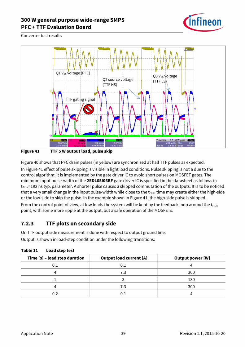
Figure 41 TTF 5 W output load, pulse skip
Figure 40 shows that PFC drain pulses (in yellow) are synchronized at half TTF pulses as expected.
In Figure 41 effect of pulse skipping is visible in light load conditions. Pulse skipping is not a due to the
control algorithm: it is implemented by the gate driver IC to avoid short pulses on MOSFET gates. The minimum input pulse-width of the 2EDL05I06BF gate driver IC is specified in the datasheet as follows in
tFILIN=192 ns typ. parameter. A shorter pulse causes a skipped commutation of the outputs. It is to be noticed
that a very small change in the input pulse-width while close to the tFILIN time may create either the high-side or the low-side to skip the pulse. In the example shown in Figure 41, the high-side pulse is skipped.
From the control point of view, at low loads the system will be kept by the feedback loop around the tFILIN
point, with some more ripple at the output, but a safe operation of the MOSFETs.
7.2.3 TTF plots on secondary side
On TTF output side measurement is done with respect to output ground line.
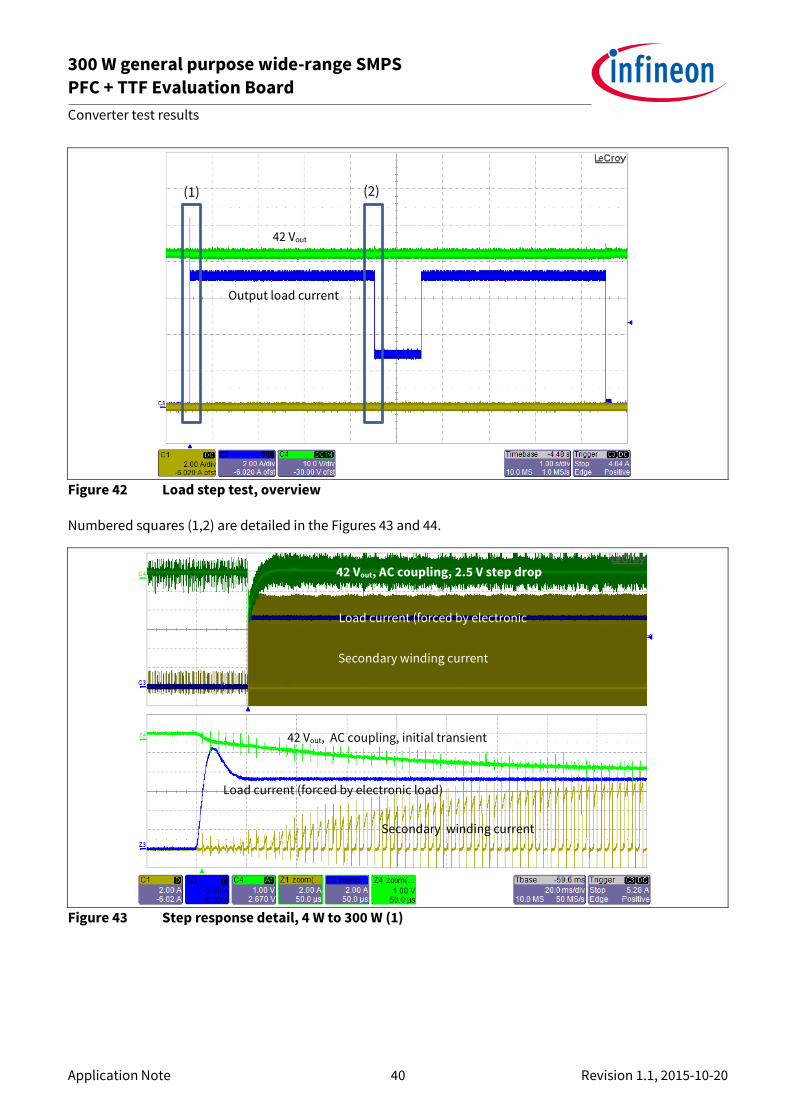
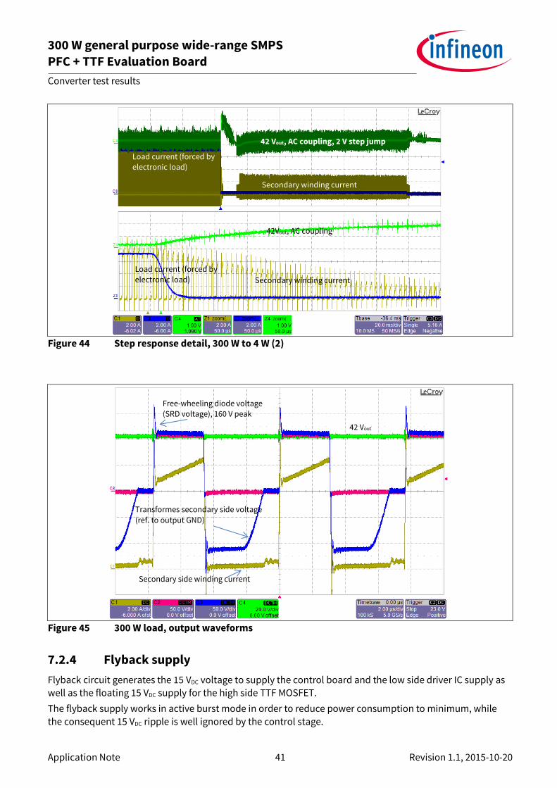
Output is shown in load-step condition under the following transitions:
Table 11 Load step test
Time [s] – load step duration Output load current [A] Output power [W]
0.1 0.1 4
4 7.3 300
1 3 130
4 7.3 300
0.2 0.1 4
Q1 VDS voltage (PFC) Q3 VDS voltage
(TTF LS) Q2 source voltage
(TTF HS)
TTF gating signal
300 W general purpose wide-range SMPS PFC + TTF Evaluation Board
Converter test results
Application Note 40 Revision 1.1, 2015-10-20
Figure 42 Load step test, overview
Numbered squares (1,2) are detailed in the Figures 43 and 44.
Figure 43 Step response detail, 4 W to 300 W (1)
42 Vout
Output load current
(1)
42 Vout, AC coupling, initial transient
42 Vout, AC coupling, 2.5 V step drop
Secondary winding current
Load current (forced by electronic load)
Load current (forced by electronic
load)
Secondary winding current
(2)
300 W general purpose wide-range SMPS PFC + TTF Evaluation Board
Converter test results
Application Note 41 Revision 1.1, 2015-10-20
Figure 44 Step response detail, 300 W to 4 W (2)
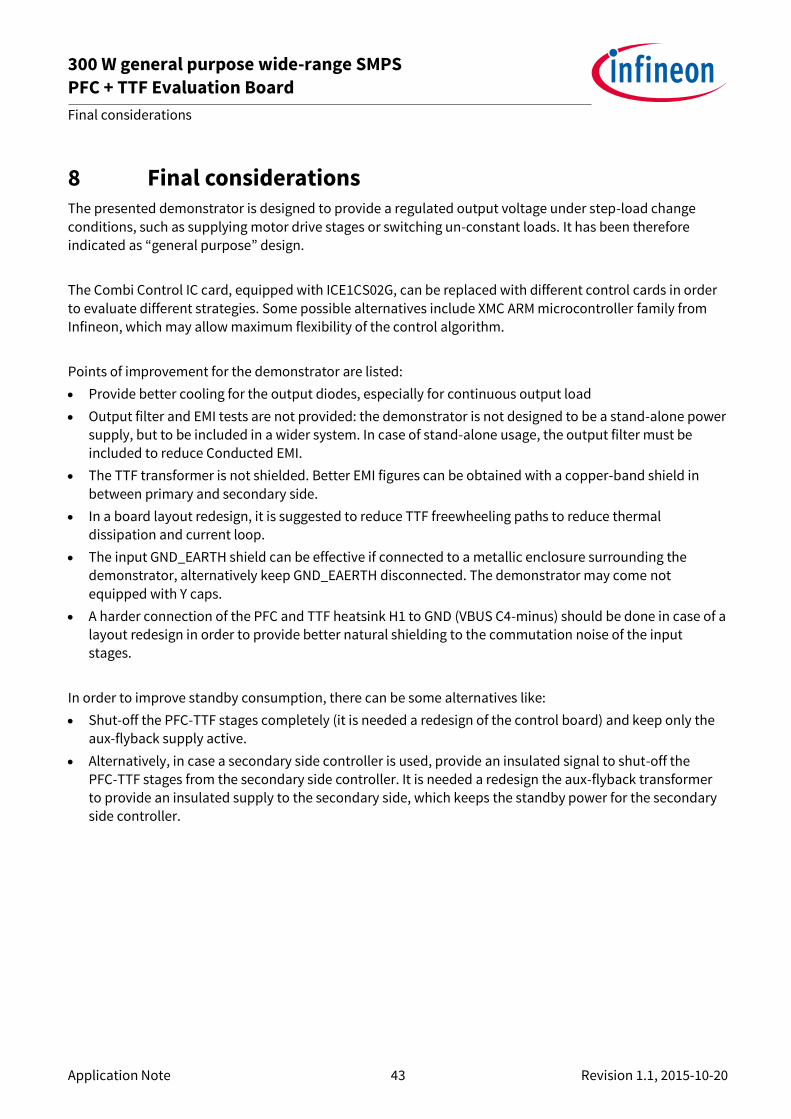
Figure 45 300 W load, output waveforms
7.2.4 Flyback supply
Flyback circuit generates the 15 VDC voltage to supply the control board and the low side driver IC supply as well as the floating 15 VDC supply for the high side TTF MOSFET.
The flyback supply works in active burst mode in order to reduce power consumption to minimum, while
the consequent 15 VDC ripple is well ignored by the control stage.
42 Vout, AC coupling, 2 V step jump
Load current (forced by electronic load)
Secondary winding current
42Vout, AC coupling
Load current (forced by electronic load) Secondary winding current
42 Vout
Free-wheeling diode voltage (SRD voltage), 160 V peak
Transformes secondary side voltage
(ref. to output GND)
Secondary side winding current
300 W general purpose wide-range SMPS PFC + TTF Evaluation Board
Converter test results
Application Note 42 Revision 1.1, 2015-10-20
Figure 46 Flyback supply waveforms
Burst frequency changes from output no-load condition to load condition, due to continuous PWM activity
at PFC and TTF stages in the second case.
Flyback waveform is taken as an example in Figure 46. There is margin to load the flyback supply up to some
Watt power.
The flyback supply is designed to start at 85 VAC input, and it is connected to 400 VDC bus.
CoolSET™ DRAIN pin voltage
15 VDC output of flyback supply for controller board
300 W general purpose wide-range SMPS PFC + TTF Evaluation Board
Final considerations
Application Note 43 Revision 1.1, 2015-10-20
8 Final considerations The presented demonstrator is designed to provide a regulated output voltage under step-load change
conditions, such as supplying motor drive stages or switching un-constant loads. It has been therefore indicated as “general purpose” design.
The Combi Control IC card, equipped with ICE1CS02G, can be replaced with different control cards in order
to evaluate different strategies. Some possible alternatives include XMC ARM microcontroller family from Infineon, which may allow maximum flexibility of the control algorithm.
Points of improvement for the demonstrator are listed:
Provide better cooling for the output diodes, especially for continuous output load
Output filter and EMI tests are not provided: the demonstrator is not designed to be a stand-alone power
supply, but to be included in a wider system. In case of stand-alone usage, the output filter must be
included to reduce Conducted EMI.
The TTF transformer is not shielded. Better EMI figures can be obtained with a copper-band shield in
between primary and secondary side.
In a board layout redesign, it is suggested to reduce TTF freewheeling paths to reduce thermal dissipation and current loop.
The input GND_EARTH shield can be effective if connected to a metallic enclosure surrounding the demonstrator, alternatively keep GND_EAERTH disconnected. The demonstrator may come not
equipped with Y caps.
A harder connection of the PFC and TTF heatsink H1 to GND (VBUS C4-minus) should be done in case of a
layout redesign in order to provide better natural shielding to the commutation noise of the input stages.
In order to improve standby consumption, there can be some alternatives like:
Shut-off the PFC-TTF stages completely (it is needed a redesign of the control board) and keep only the
aux-flyback supply active.
Alternatively, in case a secondary side controller is used, provide an insulated signal to shut-off the PFC-TTF stages from the secondary side controller. It is needed a redesign the aux-flyback transformer to provide an insulated supply to the secondary side, which keeps the standby power for the secondary side controller.
300 W general purpose wide-range SMPS PFC + TTF Evaluation Board
Bill of Material (BOM)
Application Note 44 Revision 1.1, 2015-10-20
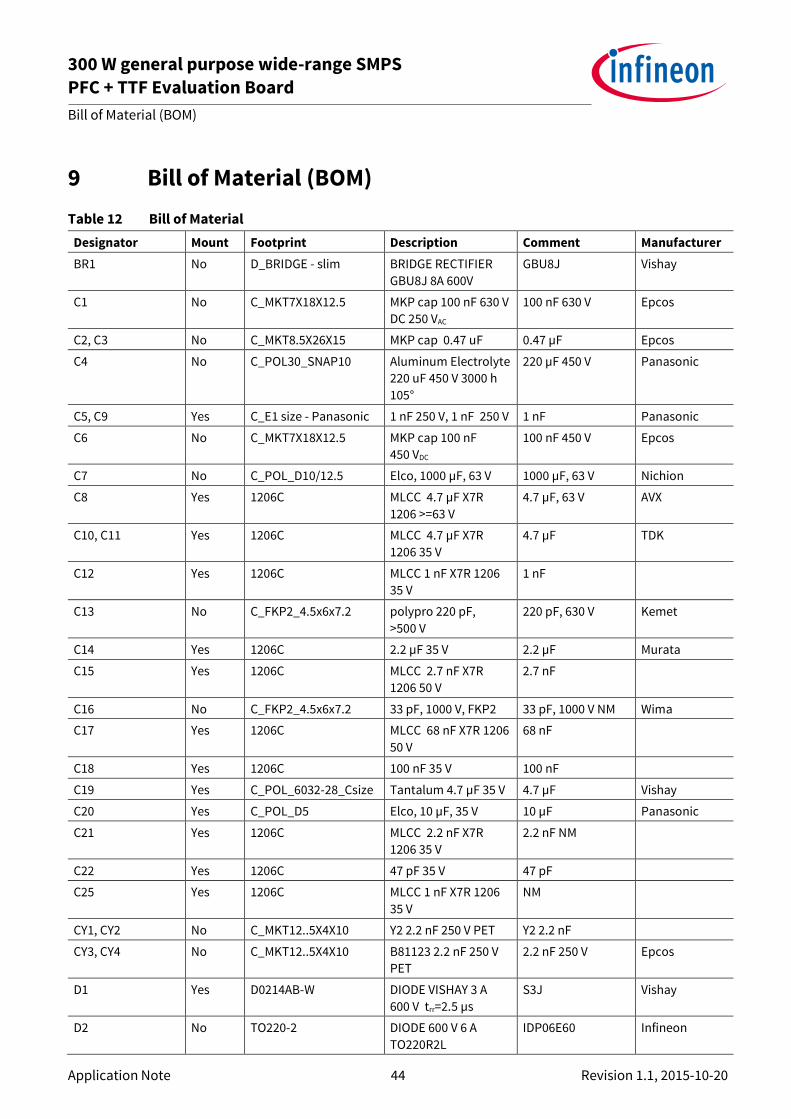
9 Bill of Material (BOM)
Table 12 Bill of Material
Designator Mount Footprint Description Comment Manufacturer
BR1 No D_BRIDGE - slim BRIDGE RECTIFIER
GBU8J 8A 600V
GBU8J Vishay
C1 No C_MKT7X18X12.5 MKP cap 100 nF 630 V
DC 250 VAC
100 nF 630 V Epcos
C2, C3 No C_MKT8.5X26X15 MKP cap 0.47 uF 0.47 µF Epcos
C4 No C_POL30_SNAP10 Aluminum Electrolyte
220 uF 450 V 3000 h
105°
220 µF 450 V Panasonic
C5, C9 Yes C_E1 size - Panasonic 1 nF 250 V, 1 nF 250 V 1 nF Panasonic
C6 No C_MKT7X18X12.5 MKP cap 100 nF
450 VDC
100 nF 450 V Epcos
C7 No C_POL_D10/12.5 Elco, 1000 µF, 63 V 1000 µF, 63 V Nichion
C8 Yes 1206C MLCC 4.7 µF X7R
1206 >=63 V
4.7 µF, 63 V AVX
C10, C11 Yes 1206C MLCC 4.7 µF X7R
1206 35 V
4.7 µF TDK
C12 Yes 1206C MLCC 1 nF X7R 1206
35 V
1 nF
C13 No C_FKP2_4.5x6x7.2 polypro 220 pF,
>500 V
220 pF, 630 V Kemet
C14 Yes 1206C 2.2 µF 35 V 2.2 µF Murata
C15 Yes 1206C MLCC 2.7 nF X7R
1206 50 V
2.7 nF
C16 No C_FKP2_4.5x6x7.2 33 pF, 1000 V, FKP2 33 pF, 1000 V NM Wima
C17 Yes 1206C MLCC 68 nF X7R 1206
50 V
68 nF
C18 Yes 1206C 100 nF 35 V 100 nF
C19 Yes C_POL_6032-28_Csize Tantalum 4.7 µF 35 V 4.7 µF Vishay
C20 Yes C_POL_D5 Elco, 10 µF, 35 V 10 µF Panasonic
C21 Yes 1206C MLCC 2.2 nF X7R
1206 35 V
2.2 nF NM
C22 Yes 1206C 47 pF 35 V 47 pF
C25 Yes 1206C MLCC 1 nF X7R 1206
35 V
NM
CY1, CY2 No C_MKT12..5X4X10 Y2 2.2 nF 250 V PET Y2 2.2 nF
CY3, CY4 No C_MKT12..5X4X10 B81123 2.2 nF 250 V
PET
2.2 nF 250 V Epcos
D1 Yes D0214AB-W DIODE VISHAY 3 A
600 V trr=2.5 µs
S3J Vishay
D2 No TO220-2 DIODE 600 V 6 A
TO220R2L
IDP06E60 Infineon
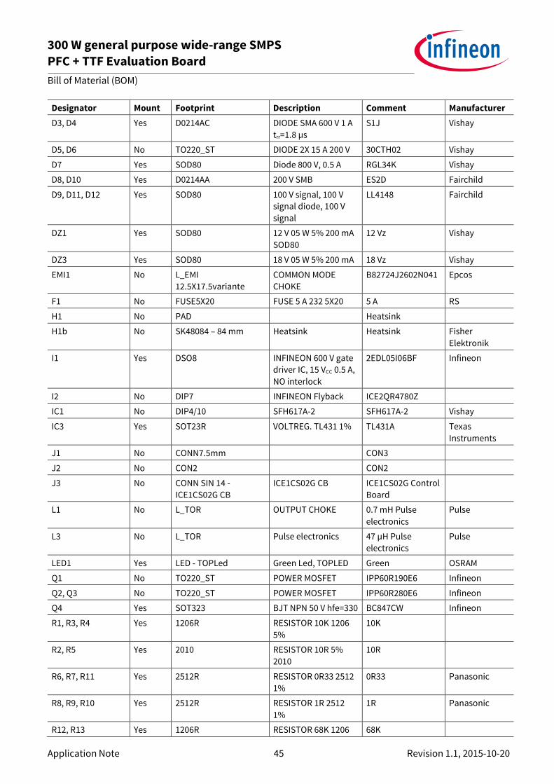
300 W general purpose wide-range SMPS PFC + TTF Evaluation Board
Bill of Material (BOM)
Application Note 45 Revision 1.1, 2015-10-20
Designator Mount Footprint Description Comment Manufacturer
D3, D4 Yes D0214AC DIODE SMA 600 V 1 A
trr=1.8 µs
S1J Vishay
D5, D6 No TO220_ST DIODE 2X 15 A 200 V 30CTH02 Vishay
D7 Yes SOD80 Diode 800 V, 0.5 A RGL34K Vishay
D8, D10 Yes D0214AA 200 V SMB ES2D Fairchild
D9, D11, D12 Yes SOD80 100 V signal, 100 V
signal diode, 100 V
signal
LL4148 Fairchild
DZ1 Yes SOD80 12 V 05 W 5% 200 mA
SOD80
12 Vz Vishay
DZ3 Yes SOD80 18 V 05 W 5% 200 mA 18 Vz Vishay
EMI1 No L_EMI
12.5X17.5variante
COMMON MODE
CHOKE
B82724J2602N041 Epcos
F1 No FUSE5X20 FUSE 5 A 232 5X20 5 A RS
H1 No PAD Heatsink
H1b No SK48084 – 84 mm Heatsink Heatsink Fisher
Elektronik
I1 Yes DSO8 INFINEON 600 V gate
driver IC, 15 VCC 0.5 A,
NO interlock
2EDL05I06BF Infineon
I2 No DIP7 INFINEON Flyback ICE2QR4780Z
IC1 No DIP4/10 SFH617A-2 SFH617A-2 Vishay
IC3 Yes SOT23R VOLTREG. TL431 1% TL431A Texas
Instruments
J1 No CONN7.5mm CON3
J2 No CON2 CON2
J3 No CONN SIN 14 -
ICE1CS02G CB
ICE1CS02G CB ICE1CS02G Control
Board
L1 No L_TOR OUTPUT CHOKE 0.7 mH Pulse
electronics
Pulse
L3 No L_TOR Pulse electronics 47 µH Pulse
electronics
Pulse
LED1 Yes LED - TOPLed Green Led, TOPLED Green OSRAM
Q1 No TO220_ST POWER MOSFET IPP60R190E6 Infineon
Q2, Q3 No TO220_ST POWER MOSFET IPP60R280E6 Infineon
Q4 Yes SOT323 BJT NPN 50 V hfe=330 BC847CW Infineon
R1, R3, R4 Yes 1206R RESISTOR 10K 1206
5%
10K
R2, R5 Yes 2010 RESISTOR 10R 5%
2010
10R
R6, R7, R11 Yes 2512R RESISTOR 0R33 2512
1%
0R33 Panasonic
R8, R9, R10 Yes 2512R RESISTOR 1R 2512
1%
1R Panasonic
R12, R13 Yes 1206R RESISTOR 68K 1206 68K
300 W general purpose wide-range SMPS PFC + TTF Evaluation Board
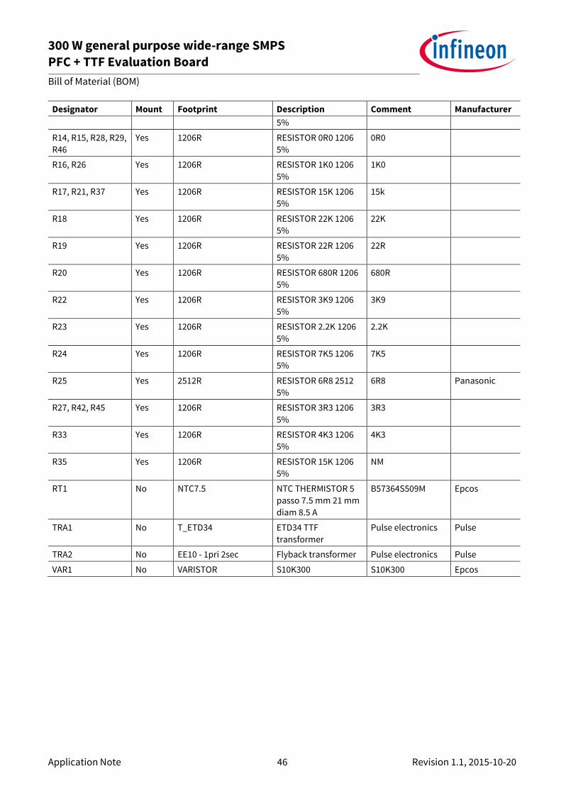
Bill of Material (BOM)
Application Note 46 Revision 1.1, 2015-10-20
Designator Mount Footprint Description Comment Manufacturer
5%
R14, R15, R28, R29,
R46
Yes 1206R RESISTOR 0R0 1206
5%
0R0
R16, R26 Yes 1206R RESISTOR 1K0 1206
5%
1K0
R17, R21, R37 Yes 1206R RESISTOR 15K 1206
5%
15k
R18 Yes 1206R RESISTOR 22K 1206
5%
22K
R19 Yes 1206R RESISTOR 22R 1206
5%
22R
R20 Yes 1206R RESISTOR 680R 1206
5%
680R
R22 Yes 1206R RESISTOR 3K9 1206
5%
3K9
R23 Yes 1206R RESISTOR 2.2K 1206
5%
2.2K
R24 Yes 1206R RESISTOR 7K5 1206
5%
7K5
R25 Yes 2512R RESISTOR 6R8 2512
5%
6R8 Panasonic
R27, R42, R45 Yes 1206R RESISTOR 3R3 1206
5%
3R3
R33 Yes 1206R RESISTOR 4K3 1206
5%
4K3
R35 Yes 1206R RESISTOR 15K 1206
5%
NM
RT1 No NTC7.5 NTC THERMISTOR 5
passo 7.5 mm 21 mm
diam 8.5 A
B57364S509M Epcos
TRA1 No T_ETD34 ETD34 TTF
transformer
Pulse electronics Pulse
TRA2 No EE10 - 1pri 2sec Flyback transformer Pulse electronics Pulse
VAR1 No VARISTOR S10K300 S10K300 Epcos

300 W general purpose wide-range SMPS PFC + TTF Evaluation Board
Appendix A: Average and rms values
Application Note 47 Revision 1.1, 2015-10-20
10 Appendix A: Average and rms values In typical electric / electronic circuits, voltage v(t) and current i(t) vary as a function of time. If a generic
function x(t) repeats with a time period T in steady state (x (t + T) = x (t)), then average function value Xavg and root-mean square (rms) value Xrms can be calculated as:
𝑋𝑎𝑣𝑔 =1
𝑇 ∙ ∫ 𝑥 (𝑡)
𝑇
0
𝑑𝑡 Eq 31
𝑋𝑟𝑚𝑠 = √ 1
𝑇 ∙ ∫ 𝑥2 (𝑡)
𝑇
0
𝑑𝑡
Eq
32
Typically, Xavg and Xrms are different; only if x (t) is constant, then Xav = Xrms. Standard waveforms (sinusoidal, rectangular and saw-tooth and triangular waves) will be further analyzed. Time origin is arbitrary, as only
periodic functions will be analyzed; eventually, offset amplitude values can be easily added by slightly
modifying formulas, as shown below.
10.1 Sinusoidal waveform
T=PeriodPeak value=XP
RMS value=XRMS
Figure 47 Nomenclature in sinusoidal function
As shown in this Figure 47, it is easy to evaluate average and rms values: average value Xavg = 0 because there
is no offset and sinusoidal waveform is positive for half period (T / 2) and negative in a simmetric way. However, rms value of a sinusoidal waveform x (t) = sin (t) is not 0, as shown below:
𝑋𝑎𝑣𝑔 =1
𝑇 ∙ ∫ 𝑥 (𝑡)
𝑇
0
𝑑𝑡 = 1
𝑇 ∙ ∫ 𝑋𝑝 ∙ 𝑠𝑖𝑛 (𝑡)
𝑇
0
𝑑𝑡 = 0 Eq 33
𝑋𝑟𝑚𝑠 = √ 1
𝑇 ∙ ∫ 𝑥2 (𝑡)
𝑇
0
𝑑𝑡 = √ 1
𝑇 ∙ ∫ (𝑋𝑝 ∙ sin(𝑡))
2𝑇
0
𝑑𝑡 = √ 1
𝑇 ∙
1
2∙ 𝑋𝑝
2 ∙ 𝑇 = 𝑋𝑝
√2
Eq 34

300 W general purpose wide-range SMPS PFC + TTF Evaluation Board
Appendix A: Average and rms values
Application Note 48 Revision 1.1, 2015-10-20
10.2 Rectangular pulse train
T=Period
t=Pulse Peak
value=XP
Figure 48 Nomenclature in pulse train function
In this case, duty cycle D = t / T makes the difference between average and rms value in a rectangular pulse train: D = [0, 1] and it is easy to understand that if D = 1, then x (t) is constant and x (t) = Xavg = Xrms = A. If D < 1,
then integrals are evaluated between 0 and t = D ∙ T.
𝑋𝑎𝑣𝑔 =1
𝑇 ∙ ∫ 𝑥 (𝑡)
𝑇
0
𝑑𝑡 =1
𝑇 ∙ ∫ 𝑋𝑃 𝑑𝑡 =
1
𝑇 ∙ 𝑋𝑃 ∙ 𝜏 = 𝑋𝑃 ∙ 𝐷
𝜏
0
Eq 35
𝑋𝑟𝑚𝑠 = √ 1
𝑇 ∙ ∫ 𝑥2 (𝑡)
𝑇
0
𝑑𝑡 = √ 1
𝑇 ∙ ∫ 𝑋𝑃
2𝜏=𝐷∙𝑇
0
𝑑𝑡 = √1
𝑇 𝑋𝑃
2 ∙ 𝐷 ∙ 𝑇 = 𝑋𝑃 ∙ √𝐷
Eq 36
10.3 Sawtooth waveform
Saw-tooth waves can be expressed analytically as:
𝑥 (𝑡) = 𝑋𝑃 ∙ 𝑡
𝜏
0 < 𝑡 < 𝜏 = 𝐷 ∙ 𝑇
𝑥 (𝑡) = 0 𝑒𝑙𝑠𝑒𝑤ℎ𝑒𝑟𝑒
Eq 37
T=Period
t=Pulse Peak
value=XP
Figure 49 Nomenclature in saw-tooth train function
Hence, Xavg and Xrms can be calculated as follows:
𝑋𝑎𝑣𝑔 =1
𝑇 ∙ ∫ 𝑥 (𝑡)
𝑇
0
𝑑𝑡 =1
𝑇 ∙ ∫ 𝑋𝑃 ∙
𝑡
𝜏 𝑑𝑡 =
1
𝑇 ∙
𝑋𝑃
𝐷 ∙ 𝑇 ∙
(𝐷 ∙ 𝑇)2
2 = 𝑋𝑃 ∙
𝐷
2
𝜏
0
Eq 38
𝑋𝑟𝑚𝑠 = √ 1
𝑇 ∙ ∫ 𝑥2 (𝑡)
𝑇
0
𝑑𝑡 = √ 1
𝑇 ∙ ∫ 𝑋𝑃
2𝜏
0
∙ (𝑡
𝜏)
2
𝑑𝑡 = 𝑋𝑃 ∙ √ 𝐷
3
Eq 39
If an offset B exists, then:

300 W general purpose wide-range SMPS PFC + TTF Evaluation Board
Appendix A: Average and rms values
Application Note 49 Revision 1.1, 2015-10-20
𝑥 (𝑡) = 𝑋𝑃 ∙ 𝑡
𝜏+ 𝐵
0 < 𝑡 < 𝜏 = 𝐷 ∙ 𝑇
𝑥 (𝑡) = 0 𝑒𝑙𝑠𝑒𝑤ℎ𝑒𝑟𝑒
Eq 40
T=Period
t=Pulse Peak
value=XP
Offset=B
Figure 50 Nomenclature saw-tooth train function with offset
Hence, Xavg and Xrms can be calculated as follows:
𝑋𝑎𝑣𝑔 =1
𝑇 ∙ ∫ 𝑥 (𝑡)
𝑇
0
𝑑𝑡 =1
𝑇 ∙ ∫ ((𝑋𝑃 − 𝐵) ∙
𝑡
𝜏+ 𝐵) 𝑑𝑡
𝜏
0
=𝐷
2∙ (𝑋𝑃 + 𝐵)
Eq 41
𝑋𝑟𝑚𝑠 = √ 1
𝑇 ∙ ∫ 𝑥2 (𝑡)
𝑇
0
𝑑𝑡 = √ 1
𝑇 ∙ ∫ ((𝑋𝑃 − 𝐵) ∙ (
𝑡
𝜏) + 𝐵)
2𝜏
0
𝑑𝑡
= √𝐷
3 ∙ √𝑋𝑃
2 + 𝑋𝑃 ∙ 𝐵 + 𝐵2
Eq 42
10.4 Triangular waveforms
Triangular waves can be expressed as:
𝑥 (𝑡) = 𝑋𝑃 ∙ 𝑡
𝜏
0 < 𝑡 < 𝜏 = 𝐷 ∙ 𝑇 Eq 43
𝑥 (𝑡) = − 𝑋𝑃 ∙ 𝑡 − 𝑇
𝑇 − 𝜏
𝜏 < 𝑡 < 𝑇
T=Period
tPeak
value=XP
Figure 51 Nomenclature in triangular train function
Xavg and Xrms can then be calculated as follows:
𝑋𝑎𝑣𝑔 =1
𝑇 ∙ ∫ 𝑥 (𝑡)
𝑇
0
𝑑𝑡 =1
𝑇 ∙ (∫ 𝑋𝑃 ∙
𝑡
𝜏 𝑑𝑡 + ∫ −𝑋𝑃 ∙
𝑡 − 𝑇
𝑇 − 𝜏
𝑇
𝜏
𝜏
0
𝑑𝑡) = 𝑋𝑃
2
Eq 44

300 W general purpose wide-range SMPS PFC + TTF Evaluation Board
Appendix A: Average and rms values
Application Note 50 Revision 1.1, 2015-10-20
𝑋𝑟𝑚𝑠 = √ 1
𝑇 ∙ ∫ 𝑥2 (𝑡)
𝑇
0
𝑑𝑡 = √ 1
𝑇 ∙ [∫ 𝑋𝑃
2𝜏
0
∙ (𝑡
𝜏)
2
𝑑𝑡 + ∫ (−𝑋𝑃 ∙ 𝑡 − 𝑇
𝑇 − 𝜏)
2𝑇
𝜏
𝑑𝑡]
=𝑋𝑃
√3
Eq 45
If an offset B exists, then:
𝑥 (𝑡) = (𝑋𝑃 − 𝐵) ∙ 𝑡
𝜏+ 𝐵
0 < 𝑡 < 𝜏 = 𝐷 ∙ 𝑇 Eq 46
𝑥 (𝑡) = −(𝑋𝑃 − 𝐵) ∙ 𝑡 − 𝑇
𝑇 − 𝜏+ 𝐵
𝜏 < 𝑡 < 𝑇
T=Period
t
Peak
value=XP
Offset=B
Figure 52 Nomenclature in triangular train function with offset
Xavg and Xrms can then be calculated as follows:
𝑋𝑎𝑣𝑔 =1
𝑇 ∙ ∫ 𝑥 (𝑡)
𝑇
0
𝑑𝑡
=1
𝑇 ∙ (∫ (𝑋𝑃 − 𝐵) ∙
𝑡
𝜏+ 𝐵 𝑑𝑡 + ∫ −(𝑋𝑃 − 𝐵) ∙
𝑡 − 𝑇
𝑇 − 𝜏
𝑇
𝜏
𝜏
0
+ 𝐵 𝑑𝑡)
= 𝑋𝑃 − 𝐵
2+ 𝐵 =
𝑋𝑃 + 𝐵
2
Eq 47
𝑋𝑟𝑚𝑠
= √ 1
𝑇 ∙ [∫ ((𝑋𝑃 − 𝐵) ∙ (
𝑡
𝜏) + 𝐵)
2𝜏
0
𝑑𝑡 + ∫ (−(𝑋𝑃 − 𝐵) ∙ 𝑡 − 𝑇
𝑇 − 𝜏+ 𝐵)
2𝑇
𝜏
𝑑𝑡]
= √1
3 ∙ √𝑋𝑃
2 + 𝑋𝑃 ∙ 𝐵 + 𝐵2
Eq 48

300 W general purpose wide-range SMPS PFC + TTF Evaluation Board
Appendix B: Chart representation of power MOSFET losses in hard switching
Application Note 51 Revision 1.1, 2015-10-20
11 Appendix B: Chart representation of power MOSFET
losses in hard switching MOSFETs selection in DC/DC applications strongly impacts on converter efficiency: transistors choice is mainly determined by power losses, which can be divided in conduction/static and switching/dynamic losses. MOSFETs conduction losses (Pstat) have been estimated by multiplying their on-resistance RDS (on) and
their squared rms drain current value ID(rms) (see Eq 49). Switching losses in MOSFETs (Pdyn) have been
calculated as described in Eq 51, where VDS is the drain-to-source voltage, Eoss (VDS) represents the energy stored in the output capacitance (Coss) and it is function of VDS, and fsw is the switching frequency. Total
power losses (Ptot) are then the sum of conduction losses Pstat and switching losses Pdyn: optimal RDS (on) for
MOSFETselection has then been evaluated by total power loss trade-off between Pstat and Pdyn.
𝑃𝑠𝑡𝑎𝑡 = 𝑅𝐷𝑆(𝑜𝑛) ∙ 𝐼𝐷(𝑟𝑚𝑠)2
Eq 49
𝑃𝑑𝑦𝑛 = 𝐸𝑜𝑠𝑠(𝑉𝐷𝑆) ∙ 𝑓𝑠𝑤 Eq 50
𝑃𝑡𝑜𝑡 = 𝑅𝐷𝑆(𝑜𝑛) ∙ 𝐼𝐷(𝑟𝑚𝑠)2 + 𝐸𝑜𝑠𝑠(𝑉𝐷𝑆) ∙ 𝑓𝑠𝑤 Eq 51
For a same technology it can be assumed that the product FOM=RDS(on)·Eoss is nearly constant while fixing the
desired VDS voltage and measurement characteristics.
This exercise is done for CoolMOS™ C6 and CoolMOS™ CE in the following tables by taking the datasheet
values.
Then Eq 51 can be rewritten as follows:
𝐹𝑂𝑀 = 𝑅𝑑𝑠(𝑜𝑛) ∙ 𝐸𝑜𝑠𝑠(𝑉𝐷𝑆) Eq 52
𝑃𝑡𝑜𝑡 = 𝑅𝐷𝑆(𝑜𝑛) ∙ 𝐼𝐷(𝑟𝑚𝑠)2 + 𝐸𝑜𝑠𝑠(𝑉𝐷𝑆) ∙ 𝑓𝑠𝑤 = 𝑅𝐷𝑆(𝑜𝑛) ∙ 𝐼𝐷(𝑟𝑚𝑠)
2 +𝐹𝑂𝑀
𝑅𝐷𝑆(𝑜𝑛)∙ 𝑓𝑠𝑤 Eq 53
Figure 53 Eoss chart for 190 mΩ CooMOS™ P6 600V IPP60R190P6
Table 13 and Table 14 shows the calculation of indicative FOM from datasheet values.

300 W general purpose wide-range SMPS PFC + TTF Evaluation Board
Appendix B: Chart representation of power MOSFET losses in hard switching
Application Note 52 Revision 1.1, 2015-10-20
Table 13 RDS(on), Eoss (@400 V) and evaluated FOM for 600 V CoolMOS™ P6 transistors
600 V CoolMOSTM P6
power transistor
RDS (on)
[mΩ]
Eoss (@ 400 V)
[µJ]
FOM (400 V) = RDS (on) ∙ Eoss
[Ω ∙ µJ]
IPP60R125P6 113 7.2 0.81
IPP60R160P6 144 5.7 0.82
IPP60R190P6 171 4.9 0.84
IPP60R230P6 207 4.2 0.87
IPP60R280P6 252 3.5 0.88
IPP60R330P6 297 3 0.89
Average 0.86
Table 14 RDS (on), Eoss (@400 V) and evaluated FOM for 500 V CoolMOS™ CE transistors
500 V CoolMOSTM CE
power transistor
RDS (on) [Ω]
Eoss
(@ 400 V/200 V)
[µJ]
FOM (@400 V/200 V) = RDS (on) ∙ Eoss
[µΩ ∙ J]
IPP50R190CE 0.17 4.4 / 2.3 0.75 / 0.39
IPP50R280CE 0.25 3.2 / 1.6 0.80 / 0.4
IPP50R380CE 0.35 2.5 / 1.2 0.87 / 0.42
IPP50R500CE 0.45 2.0 / 0.95 0.9 / 4.3
Plotting equation Eq 53 with the corresponding data, produces graphs in Figure 13 on page 15 and Figure 17
on page 20.
Note: It must be clear that the Eoss measurement is done in certain conditions, which are of course different
from the conditions found in a different design. The purpose of the above mentioned calculation is then to get a draft indication on the expected power losses in order to have a good starting point for the choice of the power mosfet.
Gate resistance and driving, as well as the stray capacitances connected to the mosfet drain will contribute to increase the calculated losses.
Additionally the counterpart freewheeling/rectifier diode, when a path is activated, have a big impact on losses, which are here neglected.

300 W general purpose wide-range SMPS PFC + TTF Evaluation Board
References and proposed links
Application Note 53 Revision 1.1, 2015-10-20
12 References and proposed links [1] CoolMOS™ high voltage MOSFETs product main page
www.infineon.com/coolmos
[2] thinQ™! Silicon Carbide Schottky Diodes main page
www.infineon.com/thinq
[3] Rapid Silicon Diodes main page
http://www.infineon.com/cms/en/product/transistor-and-diode/diode/silicon-power-diode/channel.html?channel=ff80808112ab681d0112ab6a527f04a6
[4] CoolSET™ auxiliary and SMPS controller ICs main page
www.infineon.com/coolset
[5] ICE1CS02G application note: “300W Evaluation board using ICE1CS02”:
http://www.infineon.com/dgdl?folderId=5546d4694909da4801490a2652e6286a&fileId=db3a3043
1c69a49d011c8e8e3df1048f
[6] ICE1CS02G datasheet from Infineon product page http://www.infineon.com/dgdl?folderId=5546d4694909da4801490a07012f053b&fileId=db3a3043
1c69a49d011c8e917a2d0494
[7] Addendum to 300 W general purpose wide range SMPS
http://www.infineon.com/dgdl/Infineon-
ApplicationNote_Addendum_to_300W_general_purpose_wide-range_SMPS-AN-v01_00-
EN.pdf?fileId=5546d46250cc1fdf01513392e96c3537
Revision History
Major changes since the last revision
Page or Reference Description of change
-- First Release
Revision 1.1 Alternative solution for daughterboard added; See Note on page 1

Published by
Infineon Technologies AG
81726 Munich, Germany
© 2016 Infineon Technologies AG. All Rights Reserved.
Do you have a question about any
aspect of this document?
Email: [email protected]
Document reference
Legal Disclaimer THE INFORMATION GIVEN IN THIS APPLICATION NOTE (INCLUDING BUT NOT LIMITED TO CONTENTS OF REFERENCED WEBSITES) IS GIVEN AS A HINT FOR THE IMPLEMENTATION OF THE INFINEON TECHNOLOGIES COMPONENT ONLY AND SHALL NOT BE REGARDED AS ANY DESCRIPTION OR WARRANTY OF A CERTAIN FUNCTIONALITY, CONDITION OR QUALITY OF THE INFINEON TECHNOLOGIES COMPONENT. THE RECIPIENT OF THIS APPLICATION NOTE MUST VERIFY ANY FUNCTION DESCRIBED HEREIN IN THE REAL APPLICATION. INFINEON TECHNOLOGIES HEREBY DISCLAIMS ANY AND ALL WARRANTIES AND LIABILITIES OF ANY KIND (INCLUDING WITHOUT LIMITATION WARRANTIES OF NON-INFRINGEMENT OF INTELLECTUAL PROPERTY RIGHTS OF ANY THIRD PARTY) WITH RESPECT TO ANY AND ALL INFORMATION GIVEN IN THIS APPLICATION NOTE.
Information For further information on technology, delivery terms and conditions and prices, please contact the nearest Infineon Technologies Office (www.infineon.com).
Warnings Due to technical requirements, components may contain dangerous substances. For information on the types in question, please contact the nearest Infineon Technologies Office. Infineon Technologies components may be used in life-support devices or systems only with the express written approval of Infineon Technologies, if a failure of such components can reasonably be expected to cause the failure of that life-support device or system or to affect the safety or effectiveness of that device or system. Life support devices or systems are intended to be implanted in the human body or to support and/or maintain and sustain and/or protect human life. If they fail, it is reasonable to assume that the health of the user or other persons may be endangered.
www.infineon.com
Trademarks of Infineon Technologies AG AURIX™, C166™, CanPAK™, CIPOS™, CIPURSE™, CoolGaN™, CoolMOS™, CoolSET™, CoolSiC™, CORECONTROL™, CROSSAVE™, DAVE™, DI-POL™, DrBLADE™, EasyPIM™, EconoBRIDGE™, EconoDUAL™, EconoPACK™, EconoPIM™, EiceDRIVER™, eupec™, FCOS™, HITFET™, HybridPACK™, ISOFACE™, IsoPACK™, i-Wafer™, MIPAQ™, ModSTACK™, my-d™, NovalithIC™, OmniTune™, OPTIGA™, OptiMOS™, ORIGA™, POWERCODE™, PRIMARION™, PrimePACK™, PrimeSTACK™, PROFET™, PRO-SIL™, RASIC™, REAL3™, ReverSave™, SatRIC™, SIEGET™, SIPMOS™, SmartLEWIS™, SOLID FLASH™, SPOC™, TEMPFET™, thinQ!™, TRENCHSTOP™, TriCore™.
Other Trademarks Advance Design System™ (ADS) of Agilent Technologies, AMBA™, ARM™, MULTI-ICE™, KEIL™, PRIMECELL™, REALVIEW™, THUMB™, µVision™ of ARM Limited, UK. ANSI™ of American National Standards Institute. AUTOSAR™ of AUTOSAR development partnership. Bluetooth™ of Bluetooth SIG Inc. CAT-iq™ of DECT Forum. COLOSSUS™, FirstGPS™ of Trimble Navigation Ltd. EMV™ of EMVCo, LLC (Visa Holdings Inc.). EPCOS™ of Epcos AG. FLEXGO™ of Microsoft Corporation. HYPERTERMINAL™ of Hilgraeve Incorporated. MCS™ of Intel Corp. IEC™ of Commission Electrotechnique Internationale. IrDA™ of Infrared Data Association Corporation. ISO™ of INTERNATIONAL ORGANIZATION FOR STANDARDIZATION. MATLAB™ of MathWorks, Inc. MAXIM™ of Maxim Integrated Products, Inc. MICROTEC™, NUCLEUS™ of Mentor Graphics Corporation. MIPI™ of MIPI Alliance, Inc. MIPS™ of MIPS Technologies, Inc., USA. muRata™ of MURATA MANUFACTURING CO., MICROWAVE OFFICE™ (MWO) of Applied Wave Research Inc., OmniVision™ of OmniVision Technologies, Inc. Openwave™ of Openwave Systems Inc. RED HAT™ of Red Hat, Inc. RFMD™ of RF Micro Devices, Inc. SIRIUS™ of Sirius Satellite Radio Inc. SOLARIS™ of Sun Microsystems, Inc. SPANSION™ of Spansion LLC Ltd. Symbian™ of Symbian Software Limited. TAIYO YUDEN™ of Taiyo Yuden Co. TEAKLITE™ of CEVA, Inc. TEKTRONIX™ of Tektronix Inc. TOKO™ of TOKO KABUSHIKI KAISHA TA. UNIX™ of X/Open Company Limited. VERILOG™, PALLADIUM™ of Cadence Design Systems, Inc. VLYNQ™ of Texas Instruments Incorporated. VXWORKS™, WIND RIVER™ of WIND RIVER SYSTEMS, INC. ZETEX™ of Diodes Zetex Limited. Last Trademarks Update 2014-07-17
Edition 2015-10-20
ANEVAL_201410_PL52_002