applications - chris's acorns:...
TRANSCRIPT

The FPA10 (floating point accelerator) is a single chip floating point coprocessor for ARM CPUs. It implements a subset of the ARM floating point instruction set in hardware with the remaining instructions being supported by software emulation. The combination of FPA10 hardware and support software forms an IEEE 754-1985 conformant system.
Fully IEEE 754 conformant
Fully static operation ideal for power sensitive applications
25 MHz clock operation
Low power consumption 2.5mA/MHz High performance RISC design (up to 5 MFLOPS)
Supports single, double and extended precision IEEE formats
IEEE 1149.1 Boundary scan for simplified system debug
68-pin PLCC package
Software emulator available
Applications The FPA10 will significantly enhance the performance of an ARM-based system when running floating-point intensive programs. It offers good performance from a power efficient device, for the following applications:
Computing - e.g. workstations and high performance portables. Scientific and Engineering - e.g. Finite Element Analysis. CAD - e.g. ray tracing, Gourard shading. Office Automation - e.g. relational databases, spreadsheets.

Note
In relation to IEEE 754-1985, the FPA achieves conformance in single- precision arithmetic and has an accuracy of plus or minus 2 units in the least significant place of the mantissa in double or extended precision arithmetic.
Single precision multiplications will always give a correct answer to absolute accuracy according to the IEEE 754-1985 standard.
Occasionally, double- and extended-precision multiplications may be produced with an error of 1 or 2 units in the least significant place of the mantissa.
Change Log Issue Date By Change
I 11 June 93 PLH/PM Minor changes

ARM FPA10 Data Sheet
Contents
1 Introduction 1 1.1 Coprocessor Interface 1 1.2 Instruction Issuer 2 1.3 The Load-Store Unit 2 1.4 The Register Bank 2 1.5 The Arithmetic Unit 2
2 Block Diagram 3
3 Functional Diagram 4
4 Description of Signals 5
5 Programmer's Model 7 5.1 ARM Integer and Floating Point Number Formats 8
5.1.1 Integer 8 5.1.2 IEEE Single Precision (S) 8 5.1.3 IEEE Double Precision (D) 9 5.1.4 IEEE Double Extended Precision (E) 9 5.1.5 Packed Decimal (P) 10 5.1.6 Expanded Packed Decimal (EP) 11
5.2 The Floating Point Status Register (FPSR) 12 5.2.1 System ID Byte 12 5.2.2 Exception Trap Enable Byte 13 5.23 System Control Byte 13
5.2.3.1 ND - No Denormalised Numbers Bit 13 5.2.3.2 NE - NaN Exception Bit 13 5.2.3.3 SO - Select Synchronous Operation of FPA 14 5.2.3.4 EP - Use Expanded Packed Decimal Format 14 5.2.3.5 AC - Use Alternative definition for C-flag 14
5.2.4 Exception Flags Byte 14 5.2.4.1 10 - Invalid Operation 15 5.2.4.2 DZ - Division by zero 15 5.2.4.3 OF - Overflow 15 5.2.4.4 OF - Underflow 15 5.2.4.5 IX - Inexact 16
5.3 The Floating Point Control Register (FPCR) 16
6 Floating Point Instruction Set 18
6.1 Co-Processor Data Transfer 18 6.1.1 LDF/STF - Load and Store Floating 18 6.1.2 Load and Store Multiple Floating Instructions 20
6.2 Co-Processor Data Operations 23

6.3 Co-Processor Register Transfer 25 6.3.1 Compare Operations 26
7 FPA10 Instruction Repertoire 28 7.1 Instructions implemented in FPA10 28 7.2 Instructions supported by software support code (FPASC) 29
8 Floating Point Support Code 31
8.1 IEEE Standard ConformCance 31
9 Instruction Cycle Timing 32 9.1 Performance Tuning 34
10 Boundary-Scan Test Interface 35
10.1 Overview 35 10.2 Reset 35 10.3 Instruction Register 38 10.4 Public Instructions 38
10.4.1 BYPASS (1111) 38 10.4.2 SAMPLE/PRELOAD (0011) 38 10.4.3 EXTEST (0000) 39 10.4.4 INTEST (1100) 39 10.45 IDCODE (1110) 40 10.4.6 HIGHZ (0111) 40 10.4.7 CLAMP (0101) 40 10.4.8 CLAMPZ (1001) 40
10.5 Test Data Registers 41 105.1 Bypass Register 41 10.5.2 Device Identification (ID) Code Register 41 10.5.3 Boundary-Scan (BS) Register 42
10.6 Output Enable Boundary-scan Cells 46 10.7 Single-step Operation 46 10.8 Pin information 46
11 DC Parameters 47 11.1 Absolute Maximum Ratings 47 11.2 Recommended DC Operating Conditions 48 11.3 DC Characteristics 49
12 AC Parameters 51 12.1 Test Conditions 51 12.2 Main FPA10 Signals 52 12.3 AC Characteristics 53 12.4 Boundary-Scan Interface Signals 54
13 Packaging and Pinout 56
14 Typical System Configuration 57

ARM FPA10 Data Sheet
1 Introduction
FPA10 is a floating point accelerator for the ARM family of CPUs. It has been designed so as to maximise the performance/power, performance/cost and performance/die size ratios whilst still providing a balanced floating point versus integer performance for ARM-based systems.
Typical performance in the range 2 to 5 MFlops is expected at a clock frequency of 25 MHz; actual performance is dependent on the precision selected, system configuration and the degree to which the floating point code is scheduled and otherwise optimised.
FPA10 is a single-chip floating-point coprocessor that can be used with any member of the ARM CPU family which has a coprocessor interface. It is a fully static design and its low power consumption, especially when in standby mode, makes it eminently suitable for portable and other power- and cost-sensitive applications. When used in conjunction with the supplied support code, FPA10 fully implements the IEEE Standard for Binary Floating-Point Arithmetic (ANSI/IEEE Std 754-1985).
The design of the FPA10 is based on an 81-bit internal datapath, with autonomous load /store and arithmetic units which can operate concurrently. Single, double and extended precision IEEE formats are all supported. FPA10 achieves its high performance, whilst remaining a low cost and low power solution, by employing RISC and other advanced design techniques. It is interfaced to the ARM CPU over a simple, high-performance coprocessor bus. The ARM instruction pipeline is mirrored on FPA10 so that floating point instructions can be executed directly with minimal communication overhead. Pipelining, concurrent execution units and speculative execution are all employed to improve performance without having a great impact on power consumption.
A RISC approach has been taken in selecting between those floating point instructions which are candidates for implementation in the FPA10 and those which are handled by software support. The FPA10 instruction repertoire includes only the basic operations plus compare, absolute value, round to integral value and floating-point to integer and integer to floating-point conversions. In addition, only normalised operands and zeros are handled in hardware; operations on denormalised numbers, infinities and NaNs are handled by the support code. Only the inexact exception is dealt with by hardware; all other exceptions cause the software support code to be called, whether or not the associated trap is enabled. This approach has helped to minimise the die size whilst having a negligible effect on performance in most applications.
The FPA10 includes fully compliant IEEE 1149.1 boundary-scan. The device is implemented in 1.0um double-level metal CMOS, contains about 130,000 transistors and is packaged in a 68-pin PLCC.
FPA10 consists of five main functional blocks, in addition to the clock and boundary-scan logic:
1.1 Coprocessor Interface This block is responsible for arbitrating instructions with the CPU and telling the Load-Store unit when to go ahead with data transfers.
Like ARM integer instructions, all ARM floating point instructions are conditional, obviating the need for branches for many common constructs. If a failed condition causes an instruction already issued to the Load-Store or Arithmetic unit to be skipped, then that instruction is cancelled and any results calculated
1

thus far are discarded. The same mechanism is used to cancel prefetched instructions if a branch is taken or if the ARM CPU gets interrupted before an FPA instruction has been arbitrated.
1.2 Instruction Issuer The instruction issuer is responsible for examining the incoming instruction stream and deciding whether any instructions are candidates for issuing to either the load-store unit or the arithmetic unit. Instructions can be selected from the fetch, decode or execute stages of the ARM pipeline follower. Data anti-dependency hazards (write-after-write and write-after-read) are dealt with by this unit by preventing issue until the hazard has been cleared. Instructions are issued strictly in order and only one can be issued per cycle.
1.3 The Load-Store Unit The load-store unit does the formatting and conversion necessary when moving data between the 32-bit ARM databus and the 81-bit internal register format. It is also responsible for checking all input operands and flagging any that are not normalised numbers or zero. Most subsequent operations on flagged data cause the instruction to be passed to software which will then emulate the instruction. All internal operations are performed to the internal 81-bit format.
1.4 The Register Bank The register bank contains eight 81-bit dual read-access, dual write-access registers. Data dependency hazards (read-after-write) are handled by the register control logic; read requests from either unit are stalled until the hazard is cleared. There is also a 33-bit temporary register, used by FIX, FLT and compare instructions to transfer intermediate results between the Load-Store Unit and the Arithmetic Unit. The register bank also contains logic for register-forwarding, allowing the result of one calculation to be used directly as the source for the next.
1.5 The Arithmetic Unit The arithmetic unit has a four-stage pipeline (Prepare, Calculate, Align and Round) and can speculatively execute instructions up to, but not including, register writeback. Writeback can only occur once the instruction has been arbitrated with the ARM CPU. An unusual feature of the pipeline is that each of the pipeline stages is offset by one half-cycle from the previous stage, allowing some instructions to traverse the pipeline in 2 cycles.
The Calculate stage includes a 67-bit adder, iterative array multiplier and divide unit. Fast barrel shifters are used for pre-alignment and post-normalisation.
Arithmetic operations are normally performed asynchronously to the ARM instruction stream so that an instruction is arbitrated with the CPU before FPA10 has detected whether an exception will occur. Arithmetic exceptions are therefore normally imprecise. If precise exceptions are required - for debugging purposes, for example - then a mode bit (the SO bit in the FPSR) can be set. This forces arbitration to be delayed until the arithmetic operation has completed, at the expense of a reduction in performance.
2

ARM FPA10 Data Sheet
2 Block Diagram

3 Functional Diagram

ARM FPA10 Data Sheet
4 Description of Signals
Signal I Pin I Type I Description
CPD [31: 0] 40,37-33, IT/0 Coprocessor data bus. This is a bidirectional bus which is used for 30-27,25, data transfers between FPA10 and the CPU (or memory), as follows: 24,21,20, (a) During data transfers from FPA10 to the CPU (or memory), data is 17,16,13, driven onto CPD[31:0] while CPCLK is high. 12,10-6, (b) During data transfers from the CPU (or memory) to FPA10, 3-1,68,67, CPD[31:0] are inputs and data must be setup to the falling edge of 64-61 CPCLK.
CPAOUT 42 0 Coprocessor absent output. This output is normally high, but is driven low when a floating-point instruction is being arbitrated between ARM and the FPA. CPAOUT may be connected directly to the CPA input of the CPU in a single coprocessor configuration. In a multi-coprocessor configuration, the CPAOUTs must be ANDed together to form the CPA signal. If CPA is high and nCPI is low on the rising edge of CPCLK, then ARM will take the undefined instruction trap. If CPA is low and remains low, ARM will busy-wait either (a) until CPB goes low and then complete the coprocessor instruction, or (b) until CPA goes high and then abort the instruction. CPAOUT remains low during data transfer operations (LDF, STF, LFM or SFM) until the last word of data is transferred.
CPBOUT 41 0 Coprocessor busy output. This output is normally high, but is driven low when a floating-point instruction is being arbitrated between ARM and the FPA, and the FPA is ready to accept the instruction (FPA not busy). CPBOUT maybe connected directly to the CPB input of the CPU in a single coprocessor configuration. In a multi-coprocessor configuration, the CPBOUTs must be ANDed together to form the CPB signal. ARM samples CPB on the rising edge of CPCLK if nCPI is low. CPBOUT remains low during data transfer operations (LDF, STF, LFM or SFM) until the last word of data is transferred.
CPAIN 52 IT Coprocessor absent input. Indicates to the FPA whether any other coprocessor has accepted the operation which the CPU is requesting (by asserting nCPI). In a single coprocessor system, CPAIN should be tied high. In a multiple coprocessor system, CPAIN should be con-nected directly to the CPA input of ARM. CPAIN is sampled on the rising edge of CPCLK.
CPBIN 48 IT Coprocessor busy input. Indicates to the FPA whether any other coprocessor is busy. In a single coprocessor system, CPBIN should be tied high. In a multiple coprocessor system, CPBIN should be con-nected directly to the CPB input of ARM. CPBIN is sampled on the rising edge of CPCLK.
CPCLK 46 IT Coprocessor clock. This is the FPA system clock and is also used for timing CPU/FPA interactions.
Table 1: Description of Signals
5

Signal I Pin I Type I Description
nCP I 44 IT NOT Coprocessor instruction. This input will be driven low when the CPU wishes to execute a coprocessor instruction. nCPI changes whilst CPCLK is low.
CPSPV 45 IT This input reflects the mode in which the current instruction on CPD[31:0] is being fetched by the CPU. CPSPV is high for non-user mode fetches and low for user mode fetches. CPSPV changes when CPCLK is high.
DBE 51 IT Data bus enable. When this input is low, the CPD[31:0] data bus driv- ers are put into a high impedance state. When used in an ARM600 system, DBE should be tied high.
nOPC 43 IT NOT Opcode fetch. If nOPC is low on the rising edge of CPCLK it indicates that an instruction will be available on CPD[31:0] when CPCLK next falls. nOPC is held valid when CPCLK is low, and changes when CPCLK is high.
nRESET 49 IT NOT RESET. This is a level sensitive input signal that puts the FPA into a known initial state. It will normally be connected to the CPU nRESET signal. nRESET must remain low for at least 5 CPCLK cycles.
TCK 54 ITP Test clock. Clock for IEEE 1149.1 compatible boundary scan test inter- face. TCK times all transfers on the test interface.
TDI 58 ITP Test data input. Sampled on the rising edge of TCK.
TDO 53 0 Test data output. Changes as a result of the falling edge of TCK.
TMS 57 1TP Test mode select. Changing the value of the signal driven into this input causes the Test Access Port (TAP) controller to change state. Sampled on the rising edge of TCK.
nTRST 59 ITP NOT TEST-RESET. Used to reset the test circuitry.
nWAIT 50 IT Not wait. If nWAIT is driven low, the internal clock that controls data transfers to and from the FPA will be disabled (the clock to the remainder of the FPA internal circuitry will be unaffected). This will cause the FPA interface to wait for an integer number of CPCLK cycles when slow memory devices are being accessed. nWAIT must only change when CPCLK is low. nWAIT can be used in ARM6 sys-tems; nWAIT must be tied high in ARM2 and ARM3 systems.
VDD 5,14,18,22, P Positive power supply. Nominally +5V. 31,38,56,66
vss 4,11,15,19, P Ground reference. 23,26,32, 39,47,55, 65
Table 1: Description of Signals Key to Signal Types IT Input with TTL thresholds
ITP Input with TTL thresholds and on-chip pull-up resistor 0 CMOS Output (slew-rate limited - 8mA drive) P Power
6

ARM FPA10 Data Sheet
5 Programmer's Model
The ARM IEEE floating point system has 8 high precision floating point registers, FO to F7. The working precision of the system is 80 bits, comprising a 64 bit mantissa, a 15 bit exponent and a sign bit. Specific instructions that work only with single precision operands may provide higher performance in some implementations.
There is a floating point status register (FPSR) which, like ARM's combined PC and PSR, holds all the necessary status and control information for the floating point system that an application should be able to access. It holds flags which indicate various error conditions, such as overflow and division by zero. Each flag has a corresponding trap enable bit, which can be used to enable or disable a trap associated with the error condition. Bits in the FPSR allow a client to distinguish different implementations of the floating point system and to enable or disable special features of the system.
FPA10 also contains a floating point control register (FPCR). This is used to communicate status and control information between the FPA and the FPA support code. It should be noted that the definition of the FPCR may be different for other implementations of the ARM IEEE floating point system; the FPCR may not even exist in some implementations. Software outside the floating point system should therefore not use the FPCR directly.
All basic floating point instructions operate as though the result were computed to infinite precision and then rounded to the length and in the way specified by the instruction. The rounding is selectable from:
• Round to nearest
• Round to +infinity (P)
• Round to -infinity (M)
• Round to zero (Z)
The default is round to nearest: as required by the IEEE, this rounds to nearest even for the tie case. If one of the other rounding modes is required it must be given in the instruction.
The floating point system architecture is, like ARM, "Load/Store" - the data processing operations only refer to floating point registers. Values may be stored into ARM memory in one of five formats (only four of which are visible at any one time since P and EP are mutually exclusive):
• IEEE Single Precision (S)
• IEEE Double Precision (D)
• IEEE Double Extended Precision (E)
• Packed Decimal (P)
• Expanded Packed Decimal (EP)
7

Note that in the past the layout of E format has varied between floating point systems, so software should not have been written to depend on it being readable by other floating point systems. However, for the FPA (and versions of the Floating Point Emulator (FPE) that are compatible with the FPA), the E format is now defined to be a particular form of IEEE Double Extended Precision and will not vary in future.
If it is now required to preserve register contents exactly (including signalling NaNs), then the new LFM and SFM instructions should be used. Note however that LFM and SFM should only be used for register preservation within programs and not for data which is to be transferred between programs and/or systems. The format of data stored using SFM is implementation-dependent and can generally only be restored by an LFM instruction from the same implementation.
Floating point systems may be built from software only, hardware only, or some combination of software and hardware and the results look the same to the programmer; however the supervising operating system will need to be aware of which implementation is in use to extract the best performance. Similarly, compilers can be tuned to generate bunched FP instructions for the FPE and dispersed FP instructions for the FPA to improve overall performance. The manner in which exceptions are signalled is at the discretion of the surrounding operating system.
Note that in the case of the FPA system, an exception caused by a floating point data operation or a FLT may be asynchronous (due to the nature of the ARM coprocessor interface.) Such an exception is raised some time after the instruction has started, by which time the ARM may have executed a number of instructions following the one that has failed. This means that the exact address of the instruction that caused the exception may not be identifiable. However, all the information about the exception that the IEEE Standard recommends is available.
Furthermore, in the FPA a "fully synchronous, but slow" mode of operation is available that allows the address of the faulting instruction to be determined.
Familiarity with the IEEE Standard (IEEE Standard for Binary Floating Point Arithmetic : ANSI/IEEE Std 754-1985) will be helpful in reading this datasheet.
5.1 ARM Integer and Floating Point Number Formats
5.1.1 Integer 31 0
msb 2's complement lsb
5.1.2 IEEE Single Precision (S) 31 30 23 22 0
sign Exponent msb Fraction lsb
Normalised number exponent bias = +127 Denormalised number exponent bias = +126
8

ARM FPA10 Data Sheet
5.1.3 IEEE Double Precision (D) 31 30 20 19 0
First Word sign Exponent msb Fraction (ms part) lsb
msb Fraction (Is part) lsb
Normalised number exponent bias = +1023 Denormalised number exponent bias = +1022
Single and Double values:
I Sign I Exponent I Fraction I Value represented
Quiet NaN x maximum lxxxxxxxxx IEEE Quiet NaN
Signalling NaN x maximum Onon-zero IEEE Signalling NaN
Infinity sign maximum 0000000000 (-1)sign * infinity.
Zero sign 0 0000000000 (-1) sign * 0
Denormalised no. * 2-(denorm. bias) sign 0 non-zero (-1) sig" * 0.fraction
not 0 and not (-1) sign * l.fraction Normalised no. sign maximum xxxxxxxxxx * 2(exponent - norm. bias)
5.1.4 IEEE Double Extended Precision (E)
31 30 15 14 0
First Word sgn zeros 15 bit exponent lsb
Second Word J msb Fraction (ms part) lsb
Third Word msb Fraction (Is part) lsb
J is the bit to the left of the binary point. Normalised and denormalised number exponent bias = 16383
9

Extended values:
I Sign I Exponent I J I Fraction I
Quiet NaN x maximum x lxxxxxxxxx IEEE Quiet NaN
Signalling NaN x maximum x Onon-zero IEEE Signalling NaN
Infinity sign maximum 0 0000000000 (-1)sign * infinity
Zero sign 0 0 0000000000 (-1)sign * 0
Denormalised nd11sign 0 0 non-zero (-1)sign * ()fraction * 2-(denorm.bias)
Normalised no. sign not max 1 xxxxxxxxxx (_ onn * 1.fraction
* 2(exponent - norm.bias)
** Illegal value x not 0 and not max 0 xxxxxxxxxx
** Illegal value x maximum 1 0000000000
** In general, illegal values shall not be used, although specific floating point implementations may use these bit patterns for internal purposes.
5.1.5 Packed Decimal (P) 31 0
First Word sign e3 e2 el e0 d18 d17 d16
Second Word d15 d14 d13 d12 dll d10 d9 d8
Third Word d7 d6 d5 d4 d3 d2 dl dO
Value is +/- d * 10^(+/- e). d18 and e3 are the most significant digits of d and e respectively. Sign contains both the number's sign (bit 31) and the exponent's sign (bit 30). The other bits (29,28) are 0. The value of d is arranged with the decimal point between d18 and d17, and is normalised so that for an ordinary number 1<=d18<=9. The guaranteed ranges for d and e are 17 and 3 digits respectively: e3 and dO, dl may always be zero in a particular system. The result is undefined if any of the packed digits is hexadecimal A through F.
10

ARM FPA10 Data Sheet
Packed Decimal values:
Sign - top 1 Sign - next bit bit
Exponent Digit values
Quiet NaN x x FH-4-. d8>7, rest non-zero
Signalling NaN x x F.E.H. d18<8, rest non-zero
+/- Infmity 0,1 x 1-4-1-1- all 0
+/- Zero 0,1 0 0000 all 0
Number 0,1 0,1 0000-9999 1-9.999999999999999999
All other combinations are undefined.
5.1.6 Expanded Packed Decimal (EP) 31 0
First Word sign e6 e5 e4 e3 e2 el e0
Second Word d23 d22 d21 d20 d19 d18 d17 d16
Third Word d15 d14 d13 d12 d11 d10 d9 d8
d7 d6 d5 d4 d3 d2 dl dO
Value is +/- d * 10^(+/- e). d23 and e6 are the most significant digits of d and e respectively. Sign contains both the number's sign (bit 31) and the exponent's sign (bit 30). The other bits (29,28) are 0. The value of d is arranged with the decimal point between d23 and d22, and is normalised so that for an ordinary number l<=d23<=9. The guaranteed ranges ford and e are 2FFFF4 digits respectively: e6, e5, e4 and d2FFFFdO may always be zero in a particular system. The result is undefined if any of the packed digits is hexadecimal A through F.
11

Expanded Packed Decimal values:
Sign - top Sign - next bit bit
Exponent Digit values
Quiet NaN x x 141+1-•141-.1-' d23>7, rest non-zero
Signalling NaN x x 11-.1-.1-4.1-.1' d23<8, rest non-zero
+/- Infinity 0,1 x 14-14-1-4-1. all 0
+/- Zero 0,1 0 0000000 all 0 I
Number 0,1 0,1 0-9999999 1-9.99999999999999999999999
All other combinations are undefined.
5.2 The Floating Point Status Register (FPSR) The floating point status register (FPSR) consists of a system ID byte, an exception trap enable byte, a system control byte and a cumulative exception flags byte.
Note that the FPSR is not cleared on reset. It is typically cleared by the support code using an appropriate WFS.
5.2.1 System ID Byte 31 24
Sysld
System ID byte
The 8 bit Sysld allows a user or operating system to distinguish which floating point system is in use: the top bit (bit 31) is set for HARDWARE (i.e. fast) systems, and clear for SOFTWARE (i.e. slow) systems. Note that the Sysld is read-only.
The following Sysld's are currently defined: Floating Point Emulator: 01 (HEX) (Software only) FPA10 System: 81 (HEX)
00(HEX) and 80(HEX) are also defined for pre-FPA10 software and hardware systems respectively.
12

ARM FPA10 Data Sheet
5.2.2 Exception Trap Enable Byte
23 22 21 20 19 18 17 16
Reserved IXE UFE OFE DZE IOE
Exception Trap Enable Byte
Each bit of the exception trap enable byte corresponds to one type of floating point exception. The exception types (IX,UF,OF,DZ,IO) are described below. A bit in the cumulative exception flags byte is set as a result of executing a floating point instruction only if the corresponding bit is not set in the exception trap enable byte; if the corresponding bit in the exception trap enable byte is set, then an exception trap will be taken instead of setting the exception flag. The trap handler code can then set the relevant cumulative exception bit if desired.
Normally, reserved FPSR bits should not be altered by user code. However, they may be initialised to zero.
5.2.3 System Control Byte 15 13 12 11 10 9 8
Reserved AC EP SO NE ND
System Control Byte
These control bits determine which features of the floating point system are in use. By placing these control bits in the FPSR, their state will be preserved across context switches, allowing different processes to use different features if necessary. The following five control bits are defined for the FPA system :
Bit 8: ND - No Denormalised Numbers Bit Bit 9: NE - NaN Exception Bit Bit 10: SO - Select Synchronous Operation of WA Bit 11: EP- Use Expanded Packed Decimal Format Bit 12: AC- Use Alternative definition for C-flag on compare operations
5.2.3.1 ND - No Denormalised Numbers Bit
If this bit is set, then the software will force all denormalised numbers to zero to reduce lengthy execution times when dealing with denormalised numbers. (Also known as abrupt underflow or flush to zero.) This mode is not IEEE compatible but may be required by some programs for performance reasons. If this bit is clear, then denormalised numbers will be handled in the normal IEEE-conformant way.
5.2.3.2 NE - NaN Exception Bit
When this bit is clear, extended format is regarded as an internal format as far as conversions of signalling NaNs are concerned: only conversions between single and double precision will produce an invalid operation exception because of a signalling NaN operand. This is required for compatibility with old programs which use STFE and LDFE to preserve register contents. When the NE bit is set, all conversions between single, double and extended precision will produce an invalid operation exception if the operand
13

is a signalling NaN.
5.2.3.3 SO - Select Synchronous Operation of FPA
If this bit is set, then all floating point instructions will execute synchronously and ARM will be made to busy-wait until the instruction has completed. This will allow precise exceptions to be reported but at the expense of increased execution time. If this bit is clear, then that class of floating point instructions that can execute asynchronously to ARM will do so. Exceptions that occur as a result of these instructions may then be imprecise.
5.2.3.4 EP - Use Expanded Packed Decimal Format
If this bit is set, then the expanded (four word) format will be used for Packed Decimal numbers. Use of this expanded format allows conversion from extended precision to packed decimal and back again to be carried out without loss of accuracy. If this bit is clear, then the standard (three word) format is used for Packed Decimal numbers.
5.2.3.5 AC - Use Alternative definition for C-flag on compare operations
If this bit is set, the ARM C-flag, after a compare, has the following interpretation:
C: Greater Than or Equal or Unordered
This interpretation of the C-flag allows more of the IEEE predicates to be tested by means of single ARM conditional instructions than is possible using the original interpretation of the C-flag as shown below.
If this bit is clear, the ARM C-flag, after a compare, has the following interpretation:
C: Greater Than or Equal
Normally, reserved FPSR bits should not be altered by user code. However, they may be initialised to zero.
5.2.4 Exception Flags Byte 7...5 4 3 2 1 0
Reserved IXC UFC OFC DZC IOC
Cumulative Exception Flags Byte
Whenever an exception condition arises and the corresponding trap enable bit is not set, the appropriate cumulative exception flag in bits 0 to 4 will be set to 1. If the relevant trap enable bit is set, then an exception is delivered to the user's program in a manner specific to the operating system. (Note that in the case of underflow, the state of the trap enable bit determines under which conditions the underflow exception will arise.) These flags can only be cleared by a WFS instruction.
Normally, reserved FPSR bits should not be altered by user code. However, they may be initialised to zero.
14

ARM FPA10 Data Sheet
5.2.4.1 I0 - Invalid Operation
The invalid operation exception arises when an operand is invalid for the operation to be performed. The result (if the trap is not enabled) is a quiet NaN. Invalid operations are:
• Any operation on a signalling NaN, except an LDF, LFM or SFM, or an MVF, MNF, ABS or STF without change of precision.
• Magnitude subtraction of infinities, e.g. +infinity + -infinity. • Multiplication of 0 by an infinity. • Division of 0/0 or infinity/infinity. • x REM y where x is infinity or y is 0. • Square root of any number less than zero (but SQT(-0) is -0). • Conversion to integer when overflow, infinity or NaN make it impossible. If overflow makes a
conversion to integer impossible, then the largest positive or negative integer is produced (depending on the sign of the operand) and Invalid Operation is signalled.
• CMFE, CNFE when at least one operand is a NaN. • ACS, ASN when input absolute value is > 1. • SIN, COS, TAN when input is infinite. • LOG, LGN when input < 0. • POW when first operand is < 0 and second operand is not an integer, or first operand is 0 and
second operand is <= 0. • RPW when second operand is < 0 and first operand is not an integer, or second operand is 0 and
first operand is <= 0.
5.2.4.2 DZ - Division by zero
The division by zero exception occurs if the divisor is zero and the dividend a finite, non-zero number. A correctly signed infinity is returned if the trap is disabled. DZC is also signalled for LOG(0) and LGN(0) (negative infinity is returned)
5.2.4.3 OF - Overflow
The OFC flag is set whenever the destination format's largest number is exceeded in magnitude by what would have been the rounded result were the exponent range unbounded. The untrapped result returned is the correctly signed infinity or the format's largest finite number, depending on the rounding mode.
5.2.4.4 OF - Underflow
Two correlated events contribute to underflow. These are:
(i) Tininess - the creation of a tiny non-zero result smaller in magnitude than the format's smallest normalised number.
(ii) Loss of accuracy - a loss of accuracy due to denormalisation that may be greater than would be caused by rounding alone.
If the underflow trap enable bit is set, then the underflow exception occurs when tininess is detected regardless of loss of accuracy. If the trap is disabled, then tininess and loss of accuracy must both be detected for the underflow flag to be set (in which case inexact will also be signalled).
15

5.2.4.5 IX - Inexact
The inexact exception occurs if the rounded result of an operation is not exact (i.e. different from the value computable with infinite precision), overflow has occurred while the OFE trap was disabled or underflow has occurred while the UFE trap was disabled. OFE or UFE traps take precedence over IXE. Note that, except for special cases like SIN(0) and COS(0), all transcendental operations are inexact.
5.3 The Floating Point Control Register (FPCR) The Floating Point Control register (FPCR) is an implementation-specific register : it may not exist in some versions of the ARM floating point system and, when it does exist, it may contain different information for different versions of the system. When present, it is used for internal communication within the floating point system and, in particular, to allow software and hardware components of the system to communicate with each other. Use of the WFC and RFC instructions outside the floating point system itself is strongly discouraged. In the case of User mode programs, it is actually prohibited: the WFC and RFC instructions will trap if executed in User mode.
The FPCR exists on the FPA10. It is used to enable and disable the chip and to communicate information about instructions the hardware cannot handle to the support code.
The FPA FPCR bit allocation is as follows:
31 30 29 28 27 26 25 24 23:20 19 18:16 15 14:12 11 10 9 8 7 6:5 4 3:0
RU . . IE MO EO.. OP PR SI OP DS SB AB RE DA PR RM OP S2
Bit 31 RU - Rounded Up Bit
30 Reserved
29 Reserved
28 IE - Inexact bit
27 MO - Mantissa overflow
26 EO - Exponent overflow
25 Reserved
24 Reserved 23-20;15;4 OP - AU operation code
19;7 PR - AU precision
18-16 S1 - AU source register 1
14-12 DS - AU destination register
11 SB - Store bounce : decode (R14) to get opcode
10 AB - Arithmetic bounce : opcode supplied in rest of word
9 RE - Rounding Exception : Arithmetic bounce occurred during rounding stage and destination register was written
8 DA - Disable FPA
6-5 RM - AU rounding mode
3-0 S2 - AU source register 2 (bit 3 set denotes a constant)
All defined bits are cleared on reset, except bits 8, 10, and 11 (DA, AB, and SB) which are set.
16

ARM FPA10 Data Sheet
Apart from by using the WFC instruction, the AB bit can only be set by the arithmetic unit and the SB bit can only be set by the load-store unit.
Only the arithmetic unit can write bits 31, 28:26, 23:12, 9, 7:0 of the FPCR.
The behaviour of the FPCR when the RFC and WFC instructions are executed is as follows:
• A read of the FPCR by RFC clears the SB, AB and DA bits of the FPCR, and leaves the other bits of the FPCR unchanged.
• A write of the FPCR by WFC writes the SB, AB, & DA bits of the FPCR, and leaves the other bits of the FPCR unchanged.
Note that this information about the FPCR in FPA10 is only supplied to aid with modifications to the FPA support code. Using it for any other purpose is likely to lead to compatibility problems and is strongly discouraged.
17

6 Floating Point Instruction Set
Note that not all of the instructions detailed in this chapter are implemented in hardware on the FPA10; the remainder are supported by software emulation. The details of which instructions are implemented in hardware and which in software may be found in the next chapter. Fuller details of the generic ARM Coprocessor instruction set may be found in the relevant ARM Datasheet; reference should be made to this if further clarification is required.
6.1 Co-Processor Data Transfer
6.1.1 LDF/STF - Load and Store Floating
31..28 27.24 23 22 21 20 19..16 15..12 11..8 7 0
Cond 110P U/D Y Wb L/S Rn X Fd 0001 offset
Cond - Condition field P - Pre/post indexing bit (0=post; 1=pre) U/D - Up/down bit (0=down; 1=up) Y - Transfer length (see below) Wb - Write-back bit L/S - Load/store bit (0=store to memory; 1=load from memory) Rn - Base register X - Transfer length (see below) Fd - Floating point register number offset - unsigned 8 bit immediate offset
Description Load or Store the high precision value from or to memory, using one of the five memory formats. On store the value is rounded using the round to nearest rounding method to the destination precision, or is precise if the destination has sufficient precision. Thus other rounding methods may be used by having applied a suitable floating point data operation at some time before the store - this does not compromise the requirement of rounding once only since no additional rounding error is introduced by the store instruction.
The length field is encoded into bits 22 (Y) and 15 (X) as follows:
Precision I I Y I X I FPSR.EP I Size of data format
Single S 0 0 x One Memory Word
Double D 0 1 x Two Memory Words
Extended E 1 0 x Three Memory Words
Packed Decimal P 1 1 0 Three Memory Words
Expanded Packed Decimal EP 1 1 1 Four Memory Words
18

ARM FPA10 Data Sheet
The offset in bits [7:0] is specified in words and is added to (U/D=1) or subtracted from (U/D=0) a base register (Rn), either before (P=1) or after (P=0) the base is used as the transfer address. The modified base value may be written back into the base register (Wb=1) or the old value of the base may be preserved (Wb=0).
Note that post-indexed addressing modes require explicit setting of the Wb bit, unlike LDR and STR which always write-back when post-indexed. The value of the base register, modified by the offset in a pre-indexed instruction, is used as the address for the transfer of the first word. The second word (if more than one is transferred) will go to or come from an address one word (4 bytes) higher than the first transfer, and the address will be incremented by one word for each subsequent transfer.
Assembler Syntax <LDFISTF>{cond}<SIDIEIP> Fd,[Rn]
[Rn, #<expression>]{!} [Rn],#<expression>
Pre-indexed addressing specification:
[Rn] - offset of zero [Rn, #<expression>[(!) - offset of <expression> bytes (!) Write back the base register (set the Wb bit) if ! is present.
If Rn is R15, writeback should not be specified.
Post-indexed addressing specification:
[Rn],#<expression> - offset of <expression> bytes
Note that the assembler automatically sets the Wb bit in this case. R15 should not be used as the base register where post-indexed addressing is used.
Note that the <expression> must be divisible by 4 and be in the range -1020 to 1020.
19

6.1.2 Load and Store Multiple Floating Instructions
31..28 27.24 23 22 21 20 19..16 15..12 11 8 7 0
[Cond 1110P I U/D I Y I Wb L/SI Rn X Fd100101 offset CPDT
Cond - Condition field P - Pre/post indexing bit (0=post; 1=pre) U/D - Up/down bit (0=down; l=up) Y - Register count (see below) Wb - Write-back bit L/S - Load/store bit (0=store to memory; 1=load from memory) Rn - Base register X - Register count (see below) Fd - Floating point register number offset - unsigned 8 bit immediate offset
Description The Load/Store Multiple Floating instructions allow between 1 and 4 floating point registers to be transferred from/to memory in a single operation. These operations allow groups of registers to be saved" and restored efficiently (e.g. across context switches).
The values are transferred as three words of data for each register; the data format used is not defined (and may change in future implementations), and the only legal operation that can be performed on this data is to load it back into the FPA using the same implementation's LFM instruction. The data stored in memory by an SFM instruction should not be used or modified by any user process.
Note that coprocessor number 2 (bits 11-8 in the instruction field) rather than the usual FPA coprocessor number of 1 must be used for these instructions.
The offset in bits [7:01 is specified in words and is added to (U/D=1) or subtracted from (U/D=0) a base register (Rn), either before (P=1) or after (P=0) the base is used as the transfer address. The modified base value may be written back into the base register (Wb=1) or the old value of the base may be preserved (Wb=0). Note that post-indexed addressing modes require explicit setting of the Wb bit, unlike LDR and STR which always write-back when post-indexed. The value of the base register, modified by the offset in a pre-indexed instruction, is used as the address for the transfer of the first word. The second word will go to or come from an address one word (4 bytes) higher than the first transfer, and the address will be incremented by one word for each subsequent transfer.
Assembler Syntax There are two alternative forms:
(1) <LFMISFM>.(cond) Fd,<count>,[Rn] [Rn, #<expression>]{!} [Rn],#<expression>
20

ARM FPA10 Data Sheet
The first register to transfer is specified as Fd.
The number of registers to transfer is specified in the <count> field and is encoded in Y (bit 22) and X (bit 15) as follows:
Y I X 1 No. of registers to transfer
0 1 1
1 0 2
1 1 3
0 0 4
Registers are always transferred in ascending order and wrap around at register F7. For example:
SFM F6,4,[RO] will transfer F6,F7,F0,F1 to memory starting at the address contained in register RO.
Pre-indexed addressing specification:
[Rn] - offset of zero
[Rn, #<expression>]f!) - offset of <expression> bytes
(0 Write back the base register (set the Wb bit) if ! is present.
If Rn is R15, writeback shouRn],#<expressionied.
Post-indexed addressing specification:
[Rn[,#<expression> - offset of <expression> bytes
Note that the assembler automatically sets the Wb bit in this case. R15 should not be used as the base register where post-indexed addressing is used.
Note that the <expression> must be divisible by 4 and be in the range -1020 to 1020.
(2) <LFMISFM>{cond}<FD,EA> Fd,<count>,[Rn](!)
This form of the instruction is intended for stacking type operations on the floating point registers. The following table shows how the assembler mnemonics translate into bits in the instruction.
21

Name I Stack I L bit I P bit I U bit
post-increment load LFMFD 1 0 1
pre-decrement load LFMEA 1 1 0
post-increment store SFMEA 0 0 1
pre-decrement store SFMFD 0 1 0
FD,EA define pre/post indexing and the up/down bit by reference to the form of stack required. The F and E refer to a "full" or "empty" stack, i.e. whether a pre-index has to be done (full) before storing to the stack. The A and D refer to whether the stack is ascending or descending. If ascending, an SFM will go up and LFM down; if descending, vice-versa. Note that only EA and FD are permitted: the LFM/SFM instructions are not capable of supporting empty descending or full ascending stacks.
0) Write back the base register (set the Wb bit) if ! is present.
If Rn is R15, writeback should not be specified.
22

ARM FPA10 Data Sheet
6.2 Co-Processor Data Operations
31..28 27.24 23 20 19..16 15..12 11..8 7...4 3..0
Cond 1110 abcd e Fn j Fd 0001 fgh0 i Fm CPDO
<ADF I SUF I RSF I MUF I DVF I RDF I POW I RPW>(cond}<S I DIE> (P I M I Z) Fd, Fn, <Fm I #value> <RMF I FML I FDV I FRD I POL>
<MVF I MNF I ABS I RND I SQT I LOG I LGN I EXP>(cond}<S I D I E>fP I M I Z) Fd, <Fm I #value> <SIN I COS I TAN I ASN I ACS I ATN I URD I NRM>
opcode - abcd dyadic/monadic - j (j=0 for dyadic; j=1 for monadic) destination size - of rounding mode - gh constant /Fm - i
23

abcdj I I I
00000 ADF Add Fd:=Fn+Fm
00010 MUF Multiply Fd := Fn * Fm
00100 SUF Subtract Fd := Fn - Fm
00110 RSF Reverse Subtract Fd := Fm - Fn
01000 DVF Divide Fd := Fn / Fm
r 01010 RDF Reverse Divide Fd := Fm / Fn
01100 POW Power Fd := Fn raised to the power of Fm
01110 RPW Reverse Power Fd := Fm raised to the power of Fn
10000 RMF Remainder Fd := IEEE remainder of Fn / Fm
10010 FML Fast Multiply Fd := Fn * Fm
10100 FDV r Fast Divide Fd := Fn / Fm
10110 FRD Fast Reverse Divide Fd := Fm / Fn
11000 POL Polar angle (ArcTan2) Fd := polar angle of (Fn, Fm)
11010 trap: undefined instruction
11100 trap: undefined instruction
11110 trap: undefined instruction
00001 MVF Move Fd := Fm
00011 MNF Move Negated Fd := - Fm
00101 ABS Absolute value Fd := ABS ( Fm )
00111 RND Round to integral value Fd := integer value of Fm
01001 SQT Square root Fd := square root of Fm
01011 LOG Logarithm to base 10 Fd := log io of Fm
01101 LGN Logarithm to base e Fd := loge of Fm
01111 EXP Exponent Fd:=e**Fm
10001 SIN Sine Fd := sine of Fm
10011 COS Cosine Fd := cosine of Fm
10101 TAN Tangent Fd := tangent of Fm
10111 ASN Arc Sine Fd := arcsine of Fm
11001 ACS Arc Cosine Fd := arccosine of Fm
11011 ATN Arc Tangent Fd := arctangent of Fm
11101 URD Unnormalised Round Fd := integer value of Fm, possibly in abnormal form
11111 NRM Normalise Fd := normalised form of Fm
24

ARM FPA10 Data Sheet
of suffix Destination Rounding precision
00 S IEEE Single precision 01 D IEEE Double precision 10 E IEEE Double Extended precision 11 trap: undefined instruction
Note that the precision must be specified; there is no default.
gh suffix Rounding Mode
00 Round to Nearest (default ) 01 P Round towards Plus Infinity 10 M Round towards Minus Infinity 11 Z Round towards Zero
Constants: (specified when 1=1)
i Fm Value assigned 1000 0.0 1001 1.0 1010 2.0 1011 3.0 1100 4.0 1101 5.0 1110 0.5 1111 10.0
Notes:
FML, FRD, FDV are only defined to work with single precision operands. It is not guaranteed that any particular implementation will execute the "fast" instructions any quicker than their respective "normal" versions (MUF, DVF, RDF).
Directed rounding is done only at the last stage of a SIN, COS etc. - the intermediate calculations to compute the value are done with round to nearest using the full working precision.
The URD instruction performs the IEEE "round to integer value" operation but may leave its result in an abnormal unnormalised form. The NRM instruction converts this abnormal result into a proper floating point value.
Direct use of the result of a URD instruction by any instruction other than NRM may produce unexpected results and should therefore not be done. Exception: a URD result may safely be preserved and restored by STFE /LDFE or SFM/LFM before being processed by NRM. So there is no need, for instance, to disable interrupts around a URD/NRM instruction sequence.
Similarly, the NRM instruction should only be used on a URD result. Again, use of it on other values may produce unexpected results.
25
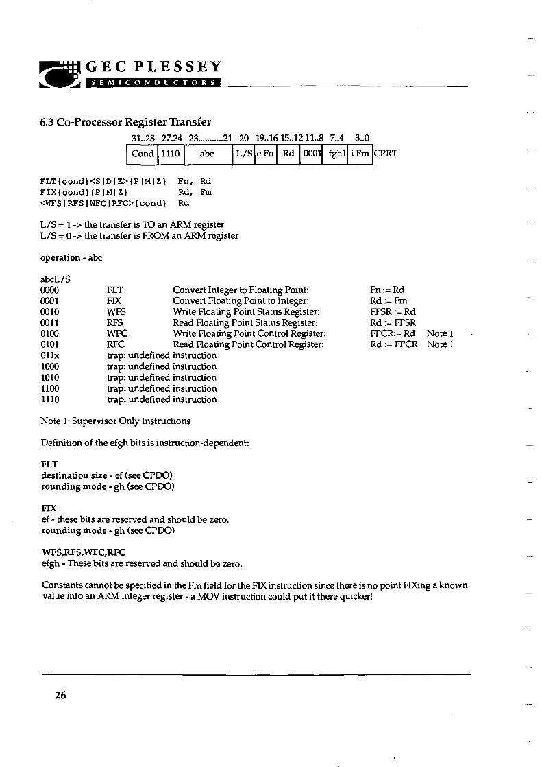
6.3 Co-Processor Register Transfer 31..28 27.24 23 21 20 19..16 15..12 11..8 7..4 3..0
I Cond 11110 I abc Lisle Fn Rd 1 0001 fghl i Fm CPRT
FLT{cond}<S ID IE>{P IMI Z} Fn, Rd FIX{cond} (1) IMIZ} Rd, Fm <WFS I RFS I WFC I RFC> { cond} Rd
L/S = 1 -> the transfer is TO an ARM register L/S = 0 -> the transfer is FROM an ARM register
operation - abc
abcL/S 0000 FLT Convert Integer to Floating Point: Fn := Rd 0001 FIX Convert Floating Point to Integer: Rd := Fm 0010 WFS Write Floating Point Status Register: FPSR := Rd 0011 RFS Read Floating Point Status Register: Rd := FPSR 0100 WFC Write Floating Point Control Register: FPCR:= Rd Note 1 0101 RFC Read Floating Point Control Register: Rd := FPCR Note 1 011x trap: undefined instruction 1000 trap: undefined instruction 1010 trap: undefined instruction 1100 trap: undefined instruction 1110 trap: undefined instruction
Note 1: Supervisor Only Instructions
Definition of the efgh bits is instruction-dependent:
FLT destination size - ef (see CPDO) rounding mode - gh (see CPDO)
FIX ef - these bits are reserved and should be zero. rounding mode - gh (see CPDO)
WFS,RFS,WFC,RFC efgh - These bits are reserved and should be zero.
Constants cannot be specified in the Fm field for the FIX instruction since there is no point FIXing a known value into an ARM integer register - a MOV instruction could put it there quicker!
26

ARM FPA10 Data Sheet
6.3.1 Compare Operations 31..28 27.24 23 21 20 19..16 15..1211..8 7..4 3..0
I Condi 11101 abc I lle Fn l 111110001) fghlii Fm
Note that these are special cases of the general CPRT instruction, with Rd = 15 and L/S = 1.
<CMF I CNF I CMFE I CNFE> (cond) Fn, Fm operation - abc constant ROM/Fm - i (see CPDO)
abc 100 CMF Compare floating: compare Fn with Fm 101 CNF Compare negated floating: compare Fn with -Fm 110 CMFE Compare floating with exception: compare Fn with Fm 111 CNFE Compare negated floating with exception: compare Fn with -Fm
efgh - These bits are reserved and should be zero.
Compares are provided with and without the exception that could arise if the numbers are unordered. When testing IEEE predicates, the CMF instruction should be used to test for equality (i.e. when a BEQ or BNE will be used afterwards) or to test for unorderedness (in the V flag). The CMFE instruction should be used for all other tests (BGT, BGE, BLT, BLE afterwards). CMFE produces an exception if the numbers are unordered, i.e. whenever at least one operand is a NaN. CMF only produces an exception when at least one operand is a signalling NaN.
The ARM flags N, Z, C, V refer to the following after compares:
If the AC bit in the FPSR is clear:
N : Less Than i.e. Fn less than Fm (or -Fm) Z : Equal C : Greater Than or Equal i.e. Fn greater than or equal to Fm ✓ : Unordered
Note that when two numbers are not equal N and C are not necessarily opposites: if the result is unordered they will both be false.
If the AC bit in the FPSR is set:
N : Less Than Z : Equal C : Greater Than or Equal or Unordered ✓ : Unordered
In this case, N and C are necessarily opposites.
27

7 FPA10 Instruction Repertoire
The FPA and support software together implement the ARM floating point instruction set as defined in the previous section. The FPA10 itself implements a subset of the instruction set as defined below.
7.1 Instructions implemented in FPA10
Mnemonic I Instructions implemented in FPAFPA10IEEE Required
LDF (S/D/E) Load (Single/Double/Extended) *
STF (S/D/E) Store (Single/Double/Extended) *
ADF Add *
SUF Subtract *
RSF Reverse Subtract
MUF Multiply
DVF Divide
RDF Reverse Divide
FML Fast Multiply
FDV Fast Divide
FRD Fast Reverse Divide
ABS Absolute
URD Round to Integral Value, possibly producing abnormal value
NRM Normalise result of URD
MVF Move *
MNF Move Negated
FLT Integer to floating point conversion *
FIX Floating point to integer conversion *
WFS Write Floating Point Status *
RFS Read Floating Point Status *
WFC Write Floating Point Control
RFC Read Floating Point Control
CMF Compare Floating
CNF Compare Negated Floating
28

ARM FPA10 Data Sheet
Mnemonic I Instructions implemented in FPA10 I IEEE Required
CMFE Compare Floating with Exception *
CNFE Compare Negated Floating with Exception
LFM Load Floating Multiple (new to FPA)
SFM Store Floating Multiple (new to FPA)
7.2 Instructions supported by software support code (FPASC)
Mnemonic I Instructions supported by software support code (FPASC) I IEEE Required
LDFP Load Packed *
STFP Store Packed *
SQT Square Root
POW Power
RPW Reverse Power
RMF Remainder *
POL Polar Angle (ArcTan2)
RND Round to Integral Value *
LOG Logarithm to base 10
LGN Logarithm to base e
EXP Exponent
SIN Sine
COS Cosine
TAN Tangent
ASN Arc Sine
ACS Arc Cosine
ATN Arc Tangent
29

The FPS will not however execute arithmetic instructions in the first list (7.1) if one or more of the operands has one of the following exceptional values (also known as uncommon values):
Infinity NaN (Not a Number) Denormalised Illegal extended precision bit patterns
In this case the instruction will be 'bounced' to the software support code for emulation.
Infinities and NaNs should occur very rarely in normal code. Slthough not common, there are a few 'normal' programs which frequently underflow and produce denormalised numbers, in which case handling of denormalised operands in software may cause a performance degradation. If necessary, this performance degradation can be minimised by setting a bit in the status register which disables support for denormalised numbers.
Certain other exceptional conditions that arise during an operation will cause the FPS to transfer that operation to the support code. These conditions include all cases of the following IEEE exceptions :
• Invalid Operation • Division by Zero • Overflow • Underflow
If the Inexact condition is detected, operation will only be transferred to the support code if the Inexact trap enable bit is set in the Floating Point Status Register. Some other rare cases (such as mantissa overflow that occurs during the rounding stage of a Store Floating instruction) that do not in fact produce an IEEE exception will also trap to the support software.
30

ARM FPA10 Data Sheet
8 Floating Point Support Code
Software support for the FPA10 includes new FPS support code (FPSSC) and a new software-only floating point emulator (FPE). The purpose of the FPSSC is threefold :
a) Emulate in software those instructions in the floating point instruction set that are not implemented in the FPS (see list above).
b) Emulate in software those instructions rejected by the FPS because they involve uncommon values.
c) Provide support for exception conditions reported by the FPS.
The FPE includes support for the new LFM and SFM instructions. The FPS system and the new FPE produce identical results; both systems are fully IEEE-conformant.
Both systems seamlessly implement the ARM floating point instruction set.
Note: This section to be expanded at a later date.
8.1 IEEE Standard Conformance The full name of the IEEE Floating Point Standard is as follows:
IEEE Standard for Binary Floating Point Arithmetic - SNSI/IEEE Std 754-1985
This is referred to as the IEEE standard or merely as IEEE in this datasheet. Note that the FPS hardware on its own will not be IEEE-conformant. Support software (the FPSSC - FPA Support Code) is required to:
a) Implement the IEEE-required operations not provided by the FPS. b) Handle operations on uncommon values which are bounced by the FPS. c) Provide exception trap-handling capability.
31

9 Instruction Cycle Timing
The following table shows the number of cycles that FPA10 takes in executing each instruction. Two numbers are given: the instruction latency and the maximum instruction throughput.
Throughput is defined to be the number of cycles between the start of an instruction and the start of a succeeding instruction of the same type, both instructions occurring in a long sequence of instructions of the same type; repeated use of the same register may only occur in a sequence of length greater than or equal to 8.
Latency is loosely defined to be the number of cycles between the start of instruction execution and its completion. The number of cycles taken by a sequence of floating point instructions, each of which depends on the result of the preceding instruction in the sequence, can generally be found by adding the latencies of the individual instructions. There may be minor discrepancies from this rule for particular sequences.
The exact definition is dependent on the type of instruction being executed:
Arithmetic instructions: From register read to register write.
LDF, LFM, FLT: From start of instruction arbitration to register write.
STF, SFM, CMF, FIX: From register read to start of next instruction arbitration.
WFS, WFC: From start of instruction arbitration until the next instruction would be deemed to start by these rules.
RFS, RFC: From the time that the previous instruction would be deemed to end by these rules to the start of the next instruction arbitration.
Note that speculative execution, concurrent execution between arithmetic and load/store instructions and concurrent execution between SRM integer instruction and FPA10 instructions can significantly reduce the effective timings shown.
Instructions can be classified into arithmetic, load/store and joint instructions as follows:
Srithmetic: Those instructions that execute completely within the arithmetic unit. These include all the hardware-implemented coprocessor data operations (see section 6.2).
Load/store: Those instructions that execute completely within the load/store unit. These include LDF, STF, LFM and SFM.
Joint: FIX, CMF,CNF,CMFE,CNFE : Srithmetic followed by load/store. FLT: Load/store followed by arithmetic. WFS,RFS,WFC,RFC: Occupy both arithmetic and load/store units, since the
arithmetic unit must be empty before any of these instructions may be executed.
32

ARM FPA10 Data Sheet
Instruction I Precision I No. registers I Throughput I Latency
LDF/STF S 2 3
LDF/STF D 3 4
LDF/STF E 4 5
LFM/SFM 1 4 5
LFM/SFM 2 7 8
LFM/SFM 3 10 11
LFM/SFM 4 13 14
MVF/MNF/ABS S/D/E 1 1 2
ADF/SUF/RSF/URD/NRM S/D/E 2 4
MUF S/D/E 8 9
FML S/D/E 5 6
DVF/RDF/FDV/FRD S 302 31 2
DVF/RDF/FDV/FRD D 582 592
DVF/RDF/FDV/FRD E 702 71 2
FLT S/D/E 6 8
FIX 8 9
CMF/CMFE/CNF/CNFE 5 6
RFS/RFC 3 43
WFS/WFC 3 3
Notes: 1 Cannot be sustained for more than 2 cycles out of every 3 cycles. 2 May be less if the division comes out exactly, causing early termination of the division
algorithm (minimum of 6 cycles throughput, 7 cycles latency). 3 May be 2 or 3 cycles, depending on the previous instruction.
33
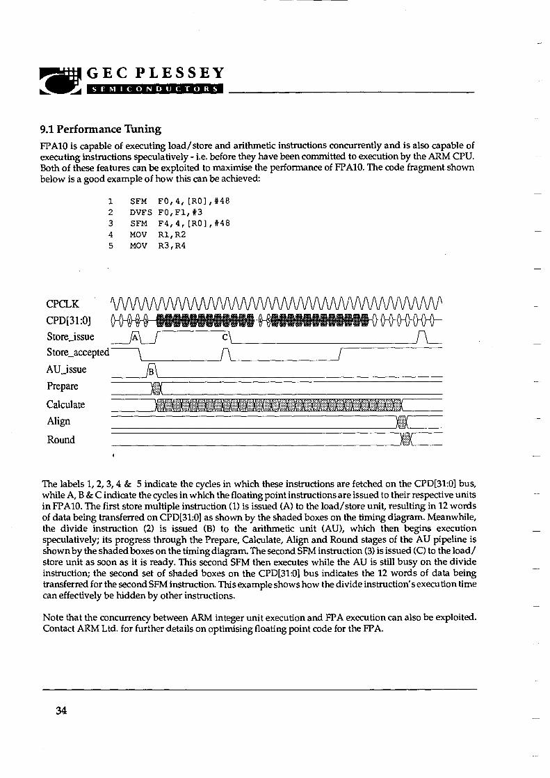
9.1 Performance Tuning FPA10 is capable of executing load/store and arithmetic instructions concurrently and is also capable of executing instructions speculatively - i.e. before they have been committed to execution by the ARM CPU. Both of these features can be exploited to maximise the performance of FPA10. The code fragment shown below is a good example of how this can be achieved:
1 SFM F0,4, [RO] , #48 2 DVFS FO, F1, #3 3 SFM F4,4, [R0], #48 4 MOV R1, R2 5 MOV R3, R4
CPCLK
CPD[31:0] 0-0-1 s
Store_issue A
Store_accepted
AU_issue
Prepare
Calculate ,
Align •
Round ()
The labels 1, 2, 3, 4 & 5 indicate the cycles in which these instructions are fetched on the CPD[31:0] bus, while A, B & C indicate the cycles in which the floating point instructions are issued to their respective units in FPA10. The first store multiple instruction (1) is issued (A) to the load/store unit, resulting in 12 words of data being transferred on CPD[31:0] as shown by the shaded boxes on the timing diagram. Meanwhile, the divide instruction (2) is issued (B) to the arithmetic unit (AU), which then begins execution speculatively; its progress through the Prepare, Calculate, Align and Round stages of the AU pipeline is shown by the shaded boxes on the timing diagram. The second SFM instruction (3) is issued (C) to the load/ store unit as soon as it is ready. This second SFM then executes while the AU is still busy on the divide instruction; the second set of shaded boxes on the CPD[31:0] bus indicates the 12 words of data being transferred for the second SFM instruction. This example shows how the divide instruction's execution time can effectively be hidden by other instructions.
Note that the concurrency between ARM integer unit execution and FPS execution can also be exploited. Contact ARM Ltd. for further details on optimising floating point code for the FPA.
34
ARM FPA10 Data Sheet
10 Boundary-Scan Test Interface
The boundary-scan interface conforms to the IEEE Std. 1149.1 - 1990, Standard Test Access Port and Boundary-Scan Architecture (please refer to this document for an explanation of the terms used in this chapter and for a description of the TAP controller states).
10.1 Overview The boundary-scan interface provides a means of testing the core of the device when it is fitted to a circuit board and a means of driving and sampling all the external pins of the device irrespective of the core state. This latter function permits testing of both the device's electrical connections to the circuit board and (in conjunction with other devices on the board having a similar interface) testing the integrity of the circuit board connections between devices. The interface intercepts all external connections within the device and each such "cell" is then connected together to form a serial register (the boundary-scan register). The whole interface is controlled via 5 dedicated pins: TDI, TMS, TCK, nTRST and TDO). In all the descriptions that follow, TDI and TMS are sampled on the rising edge of TCK and all output transitions on TDO occur following the falling edge of TCK.
10.2 Reset The boundary-scan interface includes a state-machine based controller (the TAP controller). Figure 10.2 shows the state transitions that occur in the TAP controller. In order to force the TAP controller into the correct state after power-up of the device, a reset pulse must be applied to the NTRST pin. If the boundary-scan interface is to be used, then NTRST must be driven LOW and then HIGH again. If the boundary-scan interface is not to be used, then the NTRST pin may be tied permanently LOW. Note that a LOW on NTRST causes an asynchronous reset of the boundary-scan logic and no clocking of TCK is required.
The action of test reset (either a pulse or a DC level) is as follows:
System mode is selected (i.e. the boundary-scan chain does NOT intercept any of the signals passing between the pads and the core).
IDCODE is selected as the current instruction. If TCK is pulsed, the contents of the ID register will be clocked out on TDO.
35

Figure 10.1 Boundary-Scan Block Diagram
36

ARM FPA10 Data Sheet
Figure 10.2 TAP Controller State Diagram
37

10.3 Instruction Register The instruction register is 4 bits in length.
The fixed value loaded into the instruction register during the CAPTURE-IR controller state is 0001.
10.4 Public Instructions The following public instructions are supported:
INSTRUCTION BINARY CODE
BYPASS 1111 SAMPLE/PRELOAD 0011 EXTEST 0000 INTEST 1100 IDCODE 1110 HIGHZ 0111 CLAMP 0101 CLAMPZ 1001
When loading a new instruction, the binary code should be shifted into TDI in the order least-significant to most-significant bit.
10.4.1 BYPASS (1111) The BYPASS instruction connects a 1 bit shift register (the BYPASS register) between TDI and TDO.
When the BYPASS instruction is loaded into the instruction register, all the boundary-scan cells are placed in their normal (system) mode of operation. This instruction has no effect on the system pins.
In the CAPTURE-DR state, a logic '0' is captured by the bypass register. In the SHIFT-DR state, test data is shifted into the bypass register via TDI and out via TDO after a delay of one TCK cycle. Note that the first bit shifted out will be a zero. The bypass register is not affected in the UPDATE-DR state.
10.4.2 SAMPLE/PRELOAD (0011) The BS (boundary-scan) register is placed in test mode by the SAMPLE/PRELOAD instruction.
The SAMPLE/PRELOAD instruction connects the BS register between TDI and TDO.
When the instruction register is loaded with the SAMPLE/PRELOAD instruction, all the boundary-scan cells are placed in their normal system mode of operation.
In the CAPTURE-DR state, a snapshot of the signals at the boundary-scan cells is taken on the rising edge of TCK. Normal system operation is unaffected. In the SHIFT-DR state, the sampled test data is shifted out of the BS register via the TDO pin, whilst new data is shifted in via the TDI pin to preload the BS register parallel input latch. In the UPDATE-DR state, the preloaded data is transferred into the BS register parallel output latch. Note that this data is not applied to the system logic or system pins while the SAMPLE/
38

ARM FPA10 Data Sheet
PRELOAD instruction is active. This instruction should be used to preload the boundary-scan register with known data prior to selecting the INTEST, EXTEST, CLAMP or CLAMPZ instructions; appropriate guard values to be used for each boundary-scan cell are documented in the section entitled Boundary-Scan (BS) Register.
10.4.3 EXTEST (0000) The BS (boundary-scan) register is placed in test mode by the EXTEST instruction.
The EXTEST instruction connects the BS register between TDI and TDO.
When the instruction register is loaded with the EXTEST instruction, all the boundary-scan cells are placed in their test mode of operation.
In the CAPTURE-DR state, inputs from the system pins and outputs from the boundary-scan output cells to the system pins are captured by the boundary-scan cells.
In the SHIFT-DR state, the previously captured test data is shifted out of the BS register via the TDO pin, whilst new test data is shifted in via the TDI pin to the BS register parallel input latch. In the UPDATE-DR state, the new test data is transferred into the BS register parallel output latch. Note that this data is applied immediately to the system logic and system pins.
To ensure that the core logic receives a known, stable set of inputs during EXTEST, a set of guarding values must be shifted into some of the boundary-scan cells; this guarding pattern is specified in the section entitled Boundary-Scan (BS) Register. To ensure that the guarding pattern is in place from the start of the EXTEST operation, it should be shifted into the BS register using the SAMPLE/PRELOAD instruction prior to selecting EXTEST.
10.4.4 INTEST (1100)
The BS (boundary-scan) register is placed in test mode by the INTEST instruction.
The INTEST instruction connects the BS register between TDI and TDO.
When the instruction register is loaded with the INTEST instruction, all the boundary-scan cells are placed in their test mode of operation.
In the CAPTURE-DR state, the inverse of the data supplied to the core logic from input boundary-scan cells is captured, while the true value of the data that is output from the core logic to output boundary-scan cells is captured.
In the SHIFT-DR state, the previously captured test data is shifted out of the BS register via the TDO pin, whilst new test data is shifted in via the TDI pin to the BS register parallel input latch. In the UPDATE-DR state, the new test data is transferred into the BS register parallel output latch. Note that this data is applied immediately to the system logic and system pins. The first INTEST vector should be clocked into the boundary-scan register, using the SAMPLE/PRELOAD instruction, prior to selecting INTEST to ensure that known data is applied to the system logic.
39

To ensure that the output pads are placed in a known, stable state during INTEST, a set of guarding values must be shifted into some of the boundary-scan cells; this guarding pattern is specified in the section entitled Boundary-Scan (BS) Register. To ensure that the guarding pattern is in place from the start of the INTEST operation, it should be shifted into the BS register using the SAMPLE/PRELOAD instruction prior to selecting INTEST.
Single-step operation is possible using the INTEST instruction.
10.4.5 IDCODE (1110)
The IDCODE instruction connects the device identification register (or ID register) between TDI and TDO. The ID register is a 32-bit register that allows the manufacturer, part number and version of a component to be determined through the TAP.
When the instruction register is loaded with the IDCODE instruction, all the boundary-scan cells are placed in their normal (system) mode of operation.
In the CAPTURE-DR state, the device identification code (specified in the section entitled Device Identification (ID) Code Register) is captured by the ID register. In the SHIFT-DR state, the previously captured device identification code is shifted out of the ID register via the TDO pin, whilst data is shifted in via the TDI pin into the ID register. In the UPDATE-DR state, the ID register is unaffected.
10.4.6 HIGHZ (0111)
The HIGHZ instruction connects a 1 bit shift register (the BYPASS register) between TDI and TDO.
When the HIGHZ instruction is loaded into the instruction register, all outputs are placed in an inactive drive state.
In the CAPTURE-DR state, a logic '0' is captured by the bypass register. In the SHIFT-DR state, test data is shifted into the bypass register via TDI and out via TDO after a delay of one TCK cycle. Note that the first bit shifted out will be a zero. The bypass register is not affected in the UPDATE-DR state.
10.4.7 CLAMP (0101)
The CLAMP instruction connects a 1 bit shift register (the BYPASS register) between TDI and TDO.
When the CLAMP instruction is loaded into the instruction register, the state of all output signals is defined by the values previously loaded into the boundary-scan register. A guarding pattern (specified in the section entitled Boundary-Scan (BS) Register) should be pre-loaded into the boundary-scan register using the SAMPLE/PRELOAD instruction prior to selecting the CLAMP instruction.
In the CAPTURE-DR state, a logic '0' is captured by the bypass register. In the SHIFT-DR state, test data is shifted into the bypass register via TDI and out via TDO after a delay of one TCK cycle. Note that the first bit shifted out will be a zero. The bypass register is not affected in the UPDATE-DR state.
10.4.8 CLAMPZ (1001)
The CLAMPZ instruction connects a 1 bit shift register (the BYPASS register) between TDI and TDO.
40

ARM FPA10 Data Sheet
When the CLAMPZ instruction is loaded into the instruction register, all outputs are placed in an inactive drive state, but the data supplied to the disabled output drivers is defined by the values previously loaded into the boundary-scan register. The purpose of this instruction is to ensure, during production testing, that each output driver can be disabled when its data input is either a '0' or a '1'. A guarding pattern (specified in the section entitled Boundary-Scan (BS) Register) should be pre-loaded into the boundary-scan register using the SAMPLE/PRELOAD instruction prior to selecting the CLAMPZ instruction.
In the CAPTURE-DR state, a logic '0' is captured by the bypass register. In the SHIFT-DR state, test data is shifted into the bypass register via TDI and out via TDO after a delay of one TCK cycle. Note that the first bit shifted out will be a zero. The bypass register is not affected in the UPDATE-DR state.
10.5 Test Data Registers
10.5.1 Bypass Register
Purpose: This is a single bit register which can be selected as the path between TDI and TDO to allow the device to be bypassed during boundary-scan testing.
Length: 1 bit
Operating Mode: When the Bypass instruction is the current instruction in the instruction register, serial data is transferred from TDI to TDO in the SHIFT-DR state with a delay of one TCK cycle.
There is no parallel output from the bypass register.
A logic '0' is loaded from the parallel input of the bypass register in the CAPTURE-DR state.
10.5.2 Device Identification (ID) Code Register Purpose: This register is used to read the 32-bit device identification code.
Length: 32 bits
Operating Mode: When the IDCODE instruction is current, the ID register is selected as the serial path between TDI and TDO.
There is no parallel output from the ID register.
The following 32-bit device identification code is loaded into the ID register during the CAPTURE-DR state:
Bits[31:28] : Version code = 0001 Bits[27:12] : Part number code = 1101010011000010
Bits[11:1] : Manufacturer's code = 00000110111 Bit[0] : Start bit =1
Hexadecimal value of ID code = 1D4C206F
41

10.5.3 Boundary-Scan (BS) Register Purpose: The BS register consists of a serially connected set of cells around the periphery of the device, at the interface between the system (or core) logic and the system input/output pads. This register can be used to isolate the system logic from the pins and then apply tests to the system logic, or conversely to isolate the pins from the system logic and then drive or monitor the system pins.
Length: 77 bits
Operating Modes: The BS register is selected as the register to be connected between TDI and TDO only during the SAMPLE/PRELOAD, EXTEST and INTEST instructions. Values in the BS register are used, but are not changed, during the CLAMP and CLAMPZ instructions.
In the normal (system) mode of operation, straight-through connections between the system logic and pins are maintained and normal system operation is unaffected.
In EXTEST or INTEST, values can be applied to the system logic or output pins independently of the actual values on the input pins and system logic outputs respectively. Additional boundary-scan cells are interposed in the scan chain in order to control the enabling of three-state outputs.
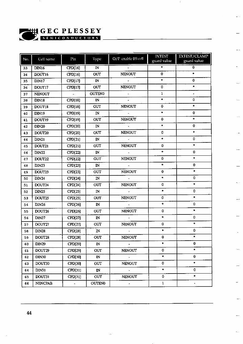
The correspondence between boundary-scan cells and system pins, system direction controls and system output enables is shown below. The cells are listed in the order in which they are connected in the boundary-scan register, starting with the cell closest to TDI. All outputs are three-state outputs. All boundary-scan register cells at input pins can apply tests to the on-chip system logic.
EXTEST/CLAMP guard values specified in the table below should be clocked into the boundary-scan register (using the SAMPLE/PRELOAD instruction) before the EXTEST, CLAMP or CLAMPZ instructions are selected to ensure that known data is applied to the system logic during the test. The INTEST guard values shown in the table below should be clocked into the boundary-scan register (using the SAMPLE/ PRELOAD instruction) before the INTEST instruction is selected to ensure that all outputs are disabled. An asterisk in the guard value col umns indicates that any value can be substituted (as the test requires), but ones and zeros should always be placed as shown.
42

ARM FPA10 Data Sheet
No. I Cell name I Pin Type 0/P enable W . •
BScell I S 1
guard value guard value
1 DINDIN00D[0] IN - * 0
2 DOUDOUT00 D[0] OUT NENOUT 0 *
3 DEN01 CPD[1] IN - * 0
4 DOUTO1 CPD[1] OUT NENOUT 0 *
5 DINO2 CPD[2] IN * 0
6 DOUTO2 CPD[2] OUT NENOUT 0 *
7 DINO3 CPD[3] IN - * 0
8 DOUTO3 CPD[3] OUT NENOUT 0 *
9 DINO4 CPD[4] IN - 0
10 DOUTO4 CPD[4] OUT NENOUT 0 *
11 DIMS CPD[5] IN - * 0
12 DOUTO5 CPD[5] OUT NENOUT 0 * .
13 DINO6 CPD[6] IN - 0
14 DOUTO6 CPD[6] OUT NENOUT 0
15 DINO7 CPD[7] IN - 0
16 DOUTO7 CPD[7] OUT NENOUT 0 *
17 DIN08 CPD[8] IN - 0
18 DOUTO8 CPD[8] OUT NENOUT 0 *
19 DINO9 CPD[9] IN - * 0 ,
20 DOUTO9 CPD[9] OUT NENOUT 0 *
21 DIN10 CPD[10] IN - 0
22 DOUT10 CPD[10] OUT NENOUT 0 *
23 DINH CPD[11] IN - * 0
24 DOUT11 CPD[11] OUT NENOUT 0
25 DIN12 CPD[12] IN - 0
26 DOUT12 CPD[12] OUT NENOUT 0
27 DIN13 CPD[13] IN - * 0
28 DOUT13 CPD[13] OUT NENOUT 0
29 DIN14 CPD[14] IN - * 0
30 DOUT14 CPD[14] OUT NENOUT 0 *
31 DIN15 CPD[15] IN - 0
32 DOUT15 CPD[15] OUT NENOUT 0 *
43
No. I Cell name I Pin I Type I 0/P enable BS cell I I NTEST I EXTEST/CLAMP guard value guard value
33 DIN16 CPD[16] IN - * 0
34 DOUT16 CPD[16] OUT NENOUT 0 *
35 DIN17 CPD[17] IN - * 0
36 DOUT17 CPD[17] OUT NENOUT 0 *
37 NENOUT - OUTENO - 1 -
38 DIN18 CPD[18] IN - * 0
39 DOUT18 CPD[18] OUT NENOUT 0 *
40 DIN19 CPD[19] IN - 0
41 DOUT19 CPD[19] OUT NENOUT 0
42 DIN20 CPD[20] IN - 0
43 DOUT20 CPD[20] OUT NENOUT 0 *
44 DIN21 CPD[21] IN - * 0
45 DOUT21 CPD[21] OUT NENOUT 0 *
4 6 D1N22 CPD[22] IN - 0
47 DOUT22 CPD[22] OUT NENOUT 0
48 DIN23 CPD[23] IN - 0
49 DOUT23 CPD[23] OUT NENOUT 0
50 DIN24 CPD[24] IN - 0
51 DOUT24 CPD[24] OUT NENOUT 0 *
52 DIN25 CPD[25] IN * 0
5 3 DOUT25 CPD[25] OUT NENOUT 0
54 DIN26 CPD[26] IN - 0
55 DOUT26 CPD[26] OUT NENOUT 0 *
56 D1N27 CPD[27] IN - * 0
57 DOUT27 CPD[27] OUT NENOUT 0
58 DIN28 CPD[28] IN - *
59 DOUT28 CPD[28] OUT NENOUT 0 *
60 DIN29 CPD[29] IN - * 0
61 DOUT29 CPD[29] OUT NENOUT 0
62 DIN30 CPD[30] IN - * 0
63 DOUT30 CPD[30] OUT NENOUT 0 *
64 DIN31 CPD[31] IN - * 0
65 DOUT31 CPD[31] OUT NENOUT 0 *
66 NENCPAB - OUTENO - 1 -
44

ARM FPA10 Data Sheet
INTEST I No. I Cell name I Pin I Type I 0/P enable BS cell I guard value
I EXTEST/CLAMP guard value
67 CPBOUT CPBOUT OUT NENCPAB 1 *
68 CPAOUT CPAOUT OUT NENCPAB 1 *
6 9 NOPC NOPC IN - * 1
7 0 NCPI NCPI IN - * 1
71 CPS PV CPSPV IN - * 1
72 CPCLK • CPCLK IN - 0
73 CPBIN CPBIN IN - * 1
74 NRESET NRESET IN - * 0
75 NWATT NWAIT IN - * 0
76 DBE DBE IN - 0
77 CPAIN CPAIN IN - * 1
KEY
NWAITput pad OUT Output pad OUTENO Output enable active low
45

10.6 Output Enable Boundary-scan Cells The following boundary-scan cells control the output drivers of three-state outputs as shown:
No I Cell Name I Pin I Type I Outputs Controlled
37 NENOUT - OUTENO CPD[31:01
66 NENCPAB - OUTENO CPAOUT, CPBOUT
In the case of type OUTENO enable cells (NENOUT & NENCPAB), loading a '1' into the cell will disable the associated drivers.
When the SAMPLE/PRELOAD or INTEST instructions are active, the value captured in the NENOUT cell will reflect the state of the NENOUT signal from the core. However, the input of the NENCPAB cell is tied permanently to Vss, so a logic '0' will always be captured by this cell if the SAMPLE/PRELOAD or INTEST instructions are active.
To put all FPA10 three-state outputs into their high impedance state, a logic '1' should be clocked into the output enable boundary-scan cells NENOUT & NENCPAB. Alternatively, the HIGHZ instruction can be used.
10.7 Single-step Operation FPA10 is a static design and there is no minimum clock speed. It can therefore be single-stepped while the INTEST instruction is selected. This can be achieved by serialising a parallel stimulus and clocking the resulting serial vectors into the boundary-scan register. When the boundary-scan register is updated, new test stimuli are applied to the core logic inputs; the effect of these stimuli can then be observed on the core logic outputs by capturing them in the boundary-scan register.
10.8 Pin information TCK, TMS, TDI and nTRST are TTL level inputs with on-chip pull up resistors, and TDO is a CMOS level output (see the chapter on DC characteristics for full details of these pins).
The TDO output should not be overdriven when active.
46

ARM FPA10 Data Sheet
11 DC Parameters - PRELIMINARY
11.1 Absolute Maximum Ratings
Symbol I Parameter I Min I Max I Units
Vdd Supply Voltage -0.3 7.0 V
Vip Voltage applied to any pin -0.3 Vdd + 0.3 V
Ta Ambient Operating Temperature -10 +80 Deg. C
Ts Storage Temperature -40 +125 Deg. C
Pd Maximum Power Dissipation 1.0 W
Notes:
These are stress ratings only. Exceeding the absolute maximum ratings may permanently damage the device. Operating the device at absolute maximum ratings for extended periods may affect device reliability. Functional operation of the device at these or any other conditions outside those specified is not implied.
The device contains circuitry designed to provide protection from damage by static discharge. It is nonetheless recommended that precautions be taken to avoid applying voltages outside the specified range.
All voltages are measured with respect to Vss.
47
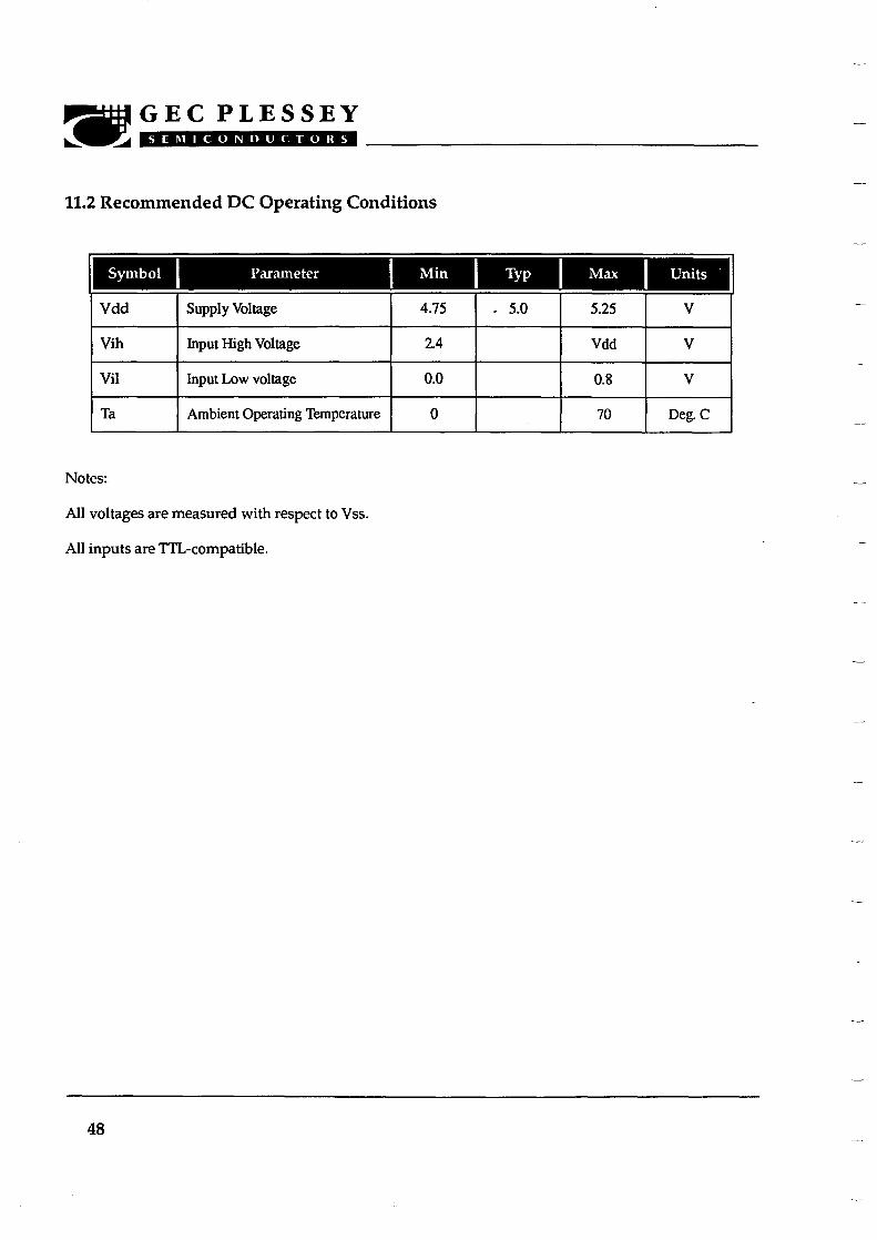
11.2 Recommended DC Operating Conditions
Symbol I Parameter I Min I Typ I Max I Units
Vdd Supply Voltage 4.75 . 5.0 5.25 V
Vih Input High Voltage 2.4 Vdd V
Vil Input Low voltage 0.0 0.8 V
Ta Ambient Operating Temperature 0 70 Deg. C
Notes:
All voltages are measured with respect to Vss.
All inputs are TTL-compatible.
48

ARM FPA10 Data Sheet
11.3 DC Characteristics - PRELIMINARY Ta = 0°C to +70°C, Vdd = 5V ± 5%
Symbol I Parameter I Typ I Units I Conditions
Idd Supply Current 100 mA
Isc Output Short Circuit Current 160 mA Note 1
Ilu D.C. Latch-up Current >200 mA Note 2
Iin IT Input Leakage Current 10 upA Note 3
Iinp ITP Input Leakage Current -500 upA Note 4
Ioh Output High Current (Vout = Vdd - 0.4V) 7 mA Note 5
lol Output Low Current (Vout = Vss + 0.4V) -11 mA Note 5
Viht Input High Voltage Threshold 2.1 V
Vilt Input Low Voltage Threshold 1.4 V
Cin Input Capacitance 5 pF Note 6
Notes:
1. Not more than one outpu10kiOhmuld be shorted to either rail at any time and for as short -a time as possible.
2. This value represents the DC current that the input/output pins can tolerate before the chip latches up. As sustained latch-up is catastrophic, this current must never be approached.
3. Input leakage current for the IT pins (TTL-level inputs).
4. Input leAage current for an ITP pin (TTL-level input Ath pull-up resistor) connected to Vss. IT? pins incorporate a pull-up resistor in the range 10ki2 - 100ka
5. Output current characteristics apply to all output pads.
6. This value includes the capacitance of the chip carrier and socket.
49

50

ARM FPA10 Data Sheet
12 AC Parameters - PRELIMINARY
12.1 Test Conditions
The AC timing diagrams presented in this section assume that the outputs of FPA10 have been loaded with the capacitive loads shown in the "Test Load" column of the table below; these loads have been chosen as typical of the system in which the FPS will be employed.
The output pads of the FPA10 are CMOS drivers which exhibit a propagation delay that increases linearly with the increase in load capacitance. An "output derating" figure is given for each output pad, showing the approximate rate of increase of output time with increasing load capacitance.
Output Signal Test Load Output derating
(pF) (nslns/pF
Xcpd[31:0] 50 0.072
Xcpaout, Xcpbout 50 0.072
51

12.2 AC Characteristics - PRELIMINARY
12.2.1 Main FPA10 Signals
52

ARM FPA10 Data Sheet
Ta = 0°C to +70°C, Vdd = 5V ± 5% - PRELIMINARY - Subject to change
Symbol I Parameter I Min I Max I Unit I Note
Tcpckl CPCLK Low Time 20 ns Note 1
Tcpckh CPCLK High Time 20 ns Note 1
Tws nWAIT setup to CPCLK 5 ns
Twh nWAIT hold from CPCLK 5 ns
Tcpins CPAIN & CPB1N setup time 10 ns
Tcpinh CPAIN & CPBIN hold time 5 ns
Tcpout CPAOUT & CPBOUT delay 20 ns
Tcpouth CPAOUT & CPBOUT hold time 5 ns
Tdbe DBE to data enable 10 ns Note 2
Tcpde CPCLK to data enable 15 ns Note 2
Tdbz DBE to data disable 15 ns Note 2
Tcpdz CPCLK to data disable 15 ns Note 2
Tcpdout Data out delay 15 ns Note 2
Tcpdoh Data out hold 5 ns Note 2
Tcpdis Data in setup 5 ns Note 2
Tcpdih Data in hold 5 ns Note 2
Tsps CPSPV setup time 5 ns
Tsph CPSPV hold time 5 ns
Tcpis nCPI setup time 5 ns
Tcpih nCPI hold time 5 ns
Topcs nOPC setup time 5 ns
Topch nOPC hold time 5 ns
Notes :
1. CPCLK timings measured between clock edges at 50% of Vdd. 2. CPD[31:0] outputs are specified to TTL levels.
53

12.2.2 Boundary-Scan Interface Signals
54

ARM FPA10 Data Sheet
(Ta = 0°C to +70°C, Vdd = 5V ± 5%) - PRELIMINARY Symbol I Parameter I Min I Typ I Max I Units I Note
Tbscl TCK low period 50 ns 1
Tbsch TCK high period 50 ns 1
Tbsis TDI,TMS setup to [TCr] 10 ns
Tbsih TDI,TMS hold from [TCr] 10 ns
Tbsoz [TCf] to TDO valid 40 ns 2
Tbsoh TDO hold time 5 ns 2
Tbsoe TDO enable time 5 ns 2,3
Tbsod TDO disable time 40 ns 2,4
Tbsss 1/0 signal setup to [TCr] 5 ns 5
Tbssh 1/0 signal hold from [TCr] 20 ns 5
Tbsdd [TCf] to data output valid 40 ns 6
Tbsdh Data output hold time 5 ns 6
Tbsde Data output enable time 5 ns 6,7
Tbsdz Data output disable time 40 ns 6,8
Tbsr Reset period 30 ns
Tbsrs TMS setup to [TRr] 10 ns 9
Tbsrh TMS hold from (TRr] 10 ns 9
Notes:
1. TCK may be stopped indefinitely in either phase. 2. Assumes a 25pF load on TDO. Output timing derates at 0.072ns/pF of extra load applied.
3. TDO enable time applies when the TAP controller enters the SHIFT-DR or SHIFT-IR states.
4. TDO disable time applies when the TAP controller leaves the SHIFT-DR or SHIFT-IR states. 5. For correct data latching, the I/O signals (from the core and the pads) must be setup and held with
respect to the rising edge of TCK in the CAPTURE-Dr state of the SAMPLE/PRELOAD, INTEST and EXTEST instructions.
6. Assumes that the data outputs are loaded with the AC test loads (see AC parameter specification). 7. Data output enable time applies when the boundary-scan logic is used to enable the output drivers.
8. Data output disable time applies when the boundary-scan logic is used to disable the output drivers. 9. The TMS input must be held high as nTRST is taken high at the end of the boundary-scan reset
sequence.
55

13 Packaging and Pinout
FPA10 is packaged in a 68-pin Plastic Leaded Chip Carrier (PLCC).
I Signal I I Signal I I Signal I I Signal I I Signal
1 CPD[6] 15 VSS 29 CPD[24] 43 nOPC 57 TMS
2 CPD[7] 16 CPD[16] 30 CPD[251 44 nCPI 58 TDI
3 CPD[8] 17 CPD[17] 31 VDD 45 CPSPV 59 nTRST
4 VSS 18 VDD 32 VSS 46 CPCLK 60 NC
5 VDD 19 VSS 33 CPD[26] 47 VSS 61 CPD[0]
6 CPD[9] 20 CPD[18] 34 CPD[271 48 CPBIN 62 CPD[1]
7 CPD[10] 21 CPD[19] 35 CPD[28] 49 nRESET 63 CPD[2]
8 CPD[11] 22 VDD 36 CPD[29] 50 nWAIT 64 CPD[3]
9 CPD[12] 23 VSS 37 CPD[30] 51 DBE 65 VSS
10 CPD[13] 24 CPD[20] 38 VDD 52 CPAIN 66 VDD
11 VSS 25 CPD[21] 39 VSS 53 TDO 67 CPD[4]
12 CPD[14] 26 VSS 40 CPD[31] 54 TCK 68 CPD[5]
13 CPD[15] 27 CPD[22] 41 CPBOUT 55 VSS
14 VDD 28 CPD[23] 42 CPAOUT 56 VDD
Note: Pin 60 is a no connect pin and should be left unconnected.
56

ARM FPA10 Data Sheet
14 Typical System Configuration
57

HEADQUARTERS OPERATIONS GEC PLESSEY SEMICONDUCTORS Cheney Manor, Swindon, Wiltshire SN2 2QW, United Kingdom. Tel: (0793) 518000 Fax: (0793) 518411
GEC PLESSEY SEMICONDUCTORS Sequoia Research Park, 1500 Green Hills Road, Scotts Valley, California 95066, United States of America. Tel: (408) 438 2900 Fax: (408) 438 5576
Manufactured under licence from Advanced RISC Machines Ltd ARM and the ARM logo are trademarks of Advanced RISC Machines Ltd
Advanced RISC Machines Ltd 1993
CUSTOMER SERVICE CENTRES • FRANCE & BENELUX Les Ulis Cedex Tel: (1) 64 46 23 45 Tx: 602858F
Fax : (1) 64 46 06 07 • GERMANY Munich Tel: (089) 3609 06-0 Tx: 523980 Fax : (089) 3609 06-55 • ITALY Milan Tel: (02) 66040867 Fax: (02) 66040993 • JAPAN Tokyo Tel: (03) 3296-0281 Fax: (03) 3296-0228 • NORTH AMERICA Integrated Circuits and Microwave Products Scotts Valley, USA
Tel (408) 438 2900 Fax: (408) 438 7023. Hybrid Products, Farmingdale, USA Tel (516) 293 8686 Fax: (516) 293 0061.
• SOUTH EAST ASIA Singapore Tel: (65) 3827708 Fax: (65) 3828872 • SWEDEN Stockholm, Tel: 46 8 702 97 70 Fax: 46 8 640 47 36 • UNITED KINGDOM & SCANDINAVIA
Swindon Tel: (0793) 518510 Tx: 444410 Fax : (0793) 518582 These are supported by Agents and Distributors in major countries world-wide.
GEC Plessey Semiconductors 1993
This pubication is issued to provide information only which (unless agreed by the Company in writing) may not be used, applied or reproduced for any purpose nor form part of any order or contract nor to be regarded as a representation relating to the products or services concerned. No warranty or guarantee express or implied is made regarding the capabiity, performance or suitabi ity of any product or service. The Company reserves the right to alter without prior knowledge the specification, design or price of any product or service. Information concerning possible methods of use is provided as a guide only and does not constitute any guarantee that such methods of use will be satisfactory in a specific piece of equipment. It is the user's responsibility to fully determine the performance and suitabilty of any equipment using such information and to ensure that any publcation or data used is up to date and has not been superseded. These products are not suitable for use in any medcal products whose failure to perform may result in significant injury
or death to the user. All products and materials are sold and services provided subject to the Company's conditions of sale, which are available on request.