atomic layer deposition for photonic crystal devices
TRANSCRIPT

ATOMIC LAYER DEPOSITION FOR PHOTONIC CRYSTAL DEVICES
E. Graugnard, J. S. King, D. Heineman, and C. J. Summers
School of Materials Science and Engineering, Georgia Institute of Technology,
Atlanta, GA, USA
Atomic Layer Deposition 2004August 16 – 18, 2004

Outline
• Introduction to Photonic Crystals• Opals• Inverse Opal
– Requirements for Photonic Band Gaps: high filling fraction, smooth, conformal, high refractive index
• Infiltration using ALD– Meets above requirements
• Results: ZnS:Mn, TiO2, Multi-layers• Summary

Photonic Crystals
x
z
y
Periodic in one direction
Periodic in two directions
Periodic in three directions
1D 2D 3D
(Joannopoulos)
• Photonic Crystal – periodic modulation of dielectric constant• Exhibits a “Photonic Band Gap” (PBG) where propagation of a range of
photon energies is forbidden.• For visible wavelengths, periodicity on order of 150 – 500 nm.• Introduction of “dielectric defects” yield modes within the PBG.• Luminescent 2D & 3D PC structures offer the potential for controlling
wavelength, efficiency, time response and threshold properties (phosphors, displays, solid state lighting, etc.).

Real Photonic Crystals:Opals & Inverse Opals
• For 3D PC’s: “top-down” approaches are difficult. – “Bottom-up” approach: self-assembly
• Most common 3D photonic crystal is the opal.– Close-packed silica spheres in air
• Opal is used as a template to create an inverse opal.– Close-packed air spheres in a dielectric material
Inverse Opal74% air for high
dielectric contrast
ALD
3D-PC Opal26% air

SiO2 Opal Films
• Opal films are polycrystalline, 10 µm thick, FCC films with the (111) planes oriented parallel to the surface.
• For visible spectrum, lattice constant ~ 140 – 500 nm.
1 µm 300 nm
Challenge: growth of uniform films within a dense, highly porous, high surface-area, FCC matrix
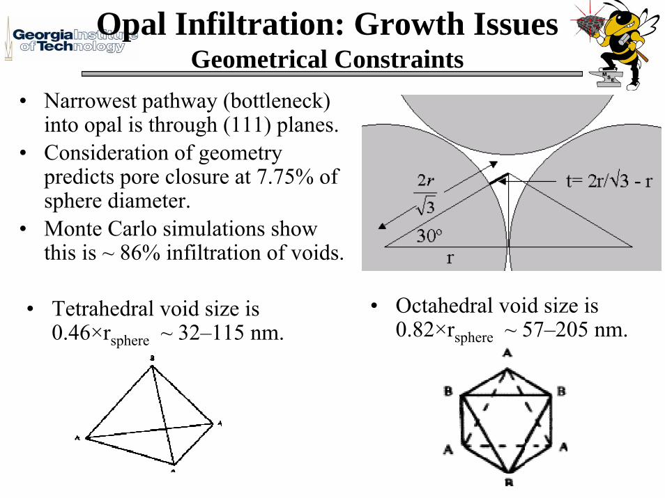
Opal Infiltration: Growth Issues Geometrical Constraints
• Narrowest pathway (bottleneck) into opal is through (111) planes.
• Consideration of geometry predicts pore closure at 7.75% of sphere diameter.
• Monte Carlo simulations show this is ~ 86% infiltration of voids.
• Octahedral void size is 0.82×rsphere ~ 57–205 nm.
• Tetrahedral void size is 0.46×rsphere ~ 32–115 nm.

Opal Films: Growth Issues Increased Surface Area
• Surface area of opal film is much larger than an equivalent planar area:
r2.22t
w4π
3π4tw0.74
AA 2
3film
opal =×
××××
=l
rr
l
• For a 10 µm thick opal film with 200 nm diameter spheres:
Aopal/Afilm = 222

Opal Infiltration:Requirements
• Uniform Infiltration– Material must be distributed uniformly throughout the opal
• Controlled Filling Fraction– Must be able to precisely control the void space filling
• Conformal and Smooth Surfaces– Creates lower porosity infiltrations– Creates air pockets at the center of the opal voids,
enhancing the PBG• High Refractive Index, Transparent, & Luminescent
Materials– For a full PBG, the refractive index contrast (with air) must
be > 2.8• ALD is the only technique to meet all of these
requirements

Inverse Opal:Fabrication
• Self-assembled silica opal template– 10 µm thick FCC polycrystalline film, (111) oriented.
• Infiltration of opal with high index materials– ZnS:Mn n~2.5 @ 425 nm (directional PBG)– TiO2 (rutile) navg~ 3.08 @ 425 nm (omni-directional PBG)
Self Assembly
ALD Etch
Sintered Opal Infiltrated Opal Inverted Opal

Opal Infiltration:Atomic Layer Deposition
• ZnS:Mn Infiltrations– Initial conditions: ZnCl2/H2S - 660ms/660ms, N2 purge - 550ms– Optimum conditions: ZnCl2/H2S – 2s/2s, N2 purge - 2s– 10s MnCl2 pulse every 100th cycle– Performed at US Army Research Laboratory (ARL) using a
Microchemistry F-120
• TiO2 Infiltrations– Initial conditions: TiCl4/H2O - 1s/1s, N2 purge - 1s– Optimum conditions: TiCl4/H2O - 4s/4s, N2 purge - 10s– Performed at Georgia Tech using a custom built hot-wall, flow-
style reactor

ALD of ZnS:Mn:Scanning Electron Microscopy
(111)
220 nm infiltrated opal
Silica Spheres ZnS:Mn
460 nm infiltrated opal
Growth Conditions: 500ºC, ZnCl2 – 660 ms, H2S – 660 ms

ALD of TiO2
(111)
300 nm
433 nm opal with TiO2crystallites deposited at 600ºC.
224 nm opal with TiO2deposited at 500ºC.
Polycrystalline TiO2 grown at high temperatures produces very rough surface coatings.
The opal structure is lost at the outer surface for complete TiO2infiltrations at high temperatures.

ALD of TiO2 at 100ºC
(111) Cross-sections
300 nm
433 nm opal infiltrated with 20 nm of TiO2
433 nm opal infiltrated with TiO2
433 nm TiO2 inverse opal
• TiO2 infiltration at 100ºC produces very smooth and conformal surface coatings with rms roughness ~2Å.
• Heat treatment (400C, 2 hrs.) of infiltrated opal converts it toanatase TiO2, increasing the refractive index from 2.35 to 2.65, with only a 2Å increase in the rms surface roughness.
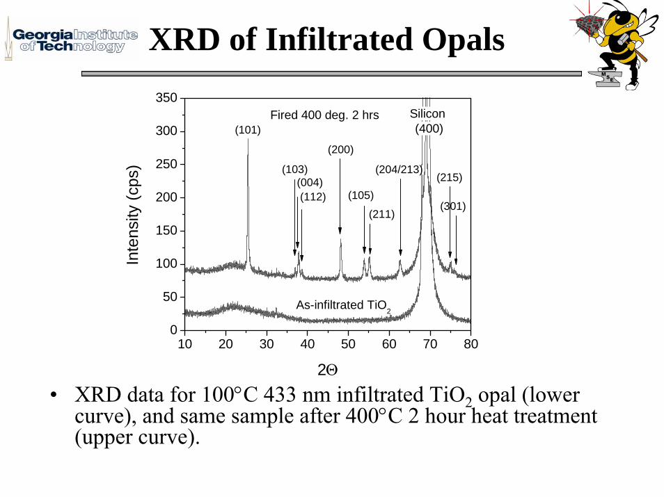
XRD of Infiltrated Opals
• XRD data for 100°C 433 nm infiltrated TiO2 opal (lower curve), and same sample after 400°C 2 hour heat treatment (upper curve).
10 20 30 40 50 60 70 800
50
100
150
200
250
300
350Fired 400 deg. 2 hrs
Inte
nsity
(cps
)
2Θ
As-infiltrated TiO2
(101)
(103)(004)(112) (105)
(200)
(211)
(204/213)(215)
(301)
Silicon (400)

Incomplete Opal Penetration
220 nm ZnS:Mn inverse opal 200 nm TiO2 inverse opal
• For small opal sphere sizes, uniform infiltration becomes difficult creating air cavities when the opal is inverted.

Optimized TiO2 Infiltration
2 µm
• Pulse and purge times were increased to optimize infiltration in opals with small sphere sizes.
433 nm TiO2 inverse opal

Anatase TiO2 Inverse Opal
FCC Brillouin zone
U
433 nm inverse opal, ion milled (111) surface

Inverse Opal Reflectivity:Theoretical Comparison
300
400
500
600
700
800
900
1000
10-11
PPBG's
Wav
elen
gth
(nm
)
Normalized Intensity
L Γ
Band Diagram
2-3 PPBG
5-68-9
Silicon Inverse Opal Photonic Band Diagram
TiO2 Inverse Opal Reflectivity and Photonic Band Diagram
n=3.5
PBG
P-PBGs
• Full PBG between bands 8 & 9• PPBGs between other bands
• 330 nm opal• ~88% filling fraction• 2.65 Refractive Index
PPBG

Precise Digital Opal Infiltration
Void filling fraction of opal as function of ALD Cycles calculated from reflectivity
TiO2 Coating Thickness as function of ALD cycles
Coa
ting
Thic
knes
s (%
radi
us)FCC (111) Pore Closure ~86%
ALD Cycles ALD Cycles
Slope: 0.039% /cycleGrowth Rate: 0.0512 nm/cycle
Voi
d S
pace
Filli
ng (%
)
• Optical verification of maximum filling fraction. • ALD allows for ultra-fine control of opal infiltration.

Multi-Layered Inverse Opal:TiO2/ZnS:Mn/TiO2
• SEM of TiO2/ZnS:Mn/TiO2inverse opal
330 nm sphere size
Luminescent multi-layered inverse opals fabricated using ALD

Photoluminescence:ZnS:Mn/TiO2 Composite
400 500 600 700 800
(f)
(c)(e)(d)
(b)
Rel
ativ
e In
tens
ity
Wavelength (nm)
(a)
∆=108%
Mn2+ Cl-
(a) 2-layer TiO2/ZnS:Mn/air (14 nm/20 nm) inverse opal
(b-f) 3-layer TiO2/ZnS:Mn/TiO2inverse opal after backfilling with TiO2 by(b) 1 nm (c) 2 nm(d) 3 nm (e) 4 nm (f) 5 nm
• 433 nm opal• 337 nm N2 laser excitation• Detection normal to surface

Summary
• Fabricated high quality inverse opal photonic crystals in the visible spectrum using ALD.
• TiO2 ALD conditions optimized for complete, uniform infiltrations with smooth and conformal coatings.– Growth/Anneal protocol developed to form anatase inverse opals
• Precise control enables novel photonic crystal structures:– Inverse opals with void space air pockets (enhanced PBG)– Achieved maximum infiltration of 86%– Perfect match between reflectivity and calculated band structure– Multi-layered luminescent inverse opals
• Modification of photoluminescence by precise infiltration– Increased Mn2+ peak intensity by 108%
• Pathway for photonic crystal band gap engineering.

Acknowledgments
• Curtis Neff• Davy Gaillot• Tsuyoshi Yamashita• US Army Research Lab: S. Blomquist, E.
Forsythe, D. Morton• Dr. Won Park, U. Colorado
• Dr. Mike Ciftan, US Army Research Office: MURI “Intelligent Luminescence for Communication, Display and Identification”