atomic layer deposition in hep
TRANSCRIPT

University of Chicago
Atomic Layer Deposition in HEP:Lessons and Opportunities
Matt Wetstein University of Chicago/ANL
presenting work of
Jeff Elam and Anil Mane Argonne National Laboratory, Material Science Division
material borrowed heavily from Mike Pellin
Argonne National Laboratory, Material Science Division
and on behalf of the Large Area Picosecond Photodector (LAPPD) Collaboration
Snowmass on the MississippiAug 2, 2013

Snowmass - August, 2013
26
What is Atomic Layer Deposition (ALD)?
Atomic Layer Deposition is a chemical vapor deposition technique based on the sequential application of two or more chemicals (precursors) that undergo self-limiting reactions with solid surfaces. This allows the application of materials, one atomic mono-layer at a time.

Snowmass - August, 2013
36
What is Atomic Layer Deposition (ALD)?
Pellin
A)
B)
Diethyl Zinc(DEZ)
H2OWater OH CH3CH3
OZn
CH3CH3
OZnCH2CH3Zn(CH2CH3)2OH
ZnO ALD Monitored UsingIn Situ Quartz Microbalance
ZnO
Thi
ckne
ss (Å
)
ZnO
Thi
ckne
ss (Å
)
ZnO ALD Thickness Measured Using Ex Situ Stylus Profiler
Growth Occurs in Discrete Steps Superb Thickness Control
OZnCH2CH3

ALD method flexibility and advantages:
20x (8”x 8”) substrates
One 200mm wafer
605/25/2011
Many parts
Multiplesubstrates
Snowmass - August, 2013
46
100 nm
ZnO
ZnOAl2O3
Al2O3
Conformal
Scalable
Can produce hybrid, layered materials
Compatible with a large number of elements and compounds
What is Atomic Layer Deposition (ALD)?

Snowmass - August, 2013
5
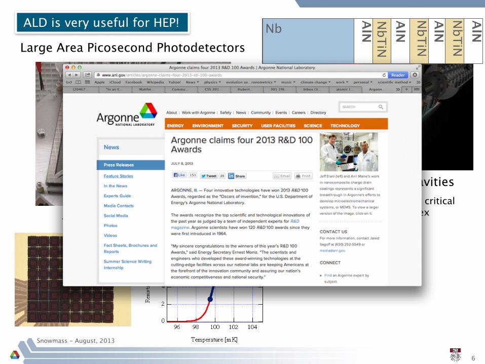
ALD is very useful for HEP! Al NbNb
AlN
NbTiN
AlN
NbTiN
AlN
AlN
NbTiN
Superconducting RF cavities•Layered structures raise the critical magnetic field at which vortex losses form.Transition Edge Sensors
7$'14,)%8(36%9:&&;%!"#$%&'()$**%
• #U;.(%#B;=%-0#V.<;%(#.;#K5%#+&/D#.O#K5%#K*+%#K.#O.-A#�%->%;L;%#(%'&F#'<;%#• #).>#ST"#0K-&>#(.2;#L=5K%;%(#K.#=<J%#GWQWW3"#/'%&-&;/%#&K#K5%#/.-;%-0#• ##U''#X#YC#/.;;%/L.;0#/.;;%/K%(#K.#%ZK%-;&'#O%%(K5-.*=50#
)*+%#.;#>-./%00#>'&R.-A#2<K5#*;0%&'%(#2<;(.2#)*+%#E9#0K&/D*>#.;#K5%#>-./%00#>'&R.-A#05.2<;=#K5%#&;.(%#0K-<>0#5..D%(#*>#&0#&##(%'&F#'<;%#
Large Area Picosecond Photodetectors
Snowmass - August, 2013
6
ALD is very useful for HEP! Al NbNb
AlN
NbTiN
AlN
NbTiN
AlN
AlN
NbTiN
Superconducting RF cavities•Layered structures raise the critical magnetic field at which vortex losses form.Transition Edge Sensors
7$'14,)%8(36%9:&&;%!"#$%&'()$**%
• #U;.(%#B;=%-0#V.<;%(#.;#K5%#+&/D#.O#K5%#K*+%#K.#O.-A#�%->%;L;%#(%'&F#'<;%#• #).>#ST"#0K-&>#(.2;#L=5K%;%(#K.#=<J%#GWQWW3"#/'%&-&;/%#&K#K5%#/.-;%-0#• ##U''#X#YC#/.;;%/L.;0#/.;;%/K%(#K.#%ZK%-;&'#O%%(K5-.*=50#
)*+%#.;#>-./%00#>'&R.-A#2<K5#*;0%&'%(#2<;(.2#)*+%#E9#0K&/D*>#.;#K5%#>-./%00#>'&R.-A#05.2<;=#K5%#&;.(%#0K-<>0#5..D%(#*>#&0#&##(%'&F#'<;%#
Large Area Picosecond Photodetectors

A new technology for neutrinos: LAPPDs
4
LAPPD: Approach Analogy
!"#$%&'(&)*$+,-.,/0$1)2$345360$3788$$$55$19$!,*)&:,);$<=.>,$$8?$
!"#$%#
&"#$%#
LAPPD: Approach
! !"#$%&'(&$)*#+(,&-$./('0',12&3*.4'&5/"(($0&60"7$&83569&&:/'7';<=0+:0*$4&&
! >$?&@#:$.72&4$*(A$(7&7/$&7$./('0',1B&$):0'*+(,&"%A"(.$#&&*(&<"7$4*"0#&#.*$(.$&"(%&$0$.74'(*.#B&%4*A$(&C1&#.*$(.$&&,'"0#&&D E=001&F(7$,4"7$%&@::4'"./&
D G"*(&"(&'4%$4&'H&<",(*7=%$&*(&"7&0$"#7&'($&:$4H'4<"(.$&&./"4".7$4*#+.&
!"#$%&'(&)*$+,-.,/0$1)2$345360$3788$$$55$19$!,*)&:,);$<=.>,$$84$
IJ&.<&
KJ&.<&
Snowmass - August, 2013
7
LAPPD Collaboration Reinventing the unit-cell of light-based neutrino detectors
• single pixel (poor spatial granularity)• nanosecond time resolution• bulky• blown glass• sensitive to magnetic fields
• millimeter-level spatial resolution• <100 picosecond time resolution• compact• standard sheet glass• operable in a magnetic field
84
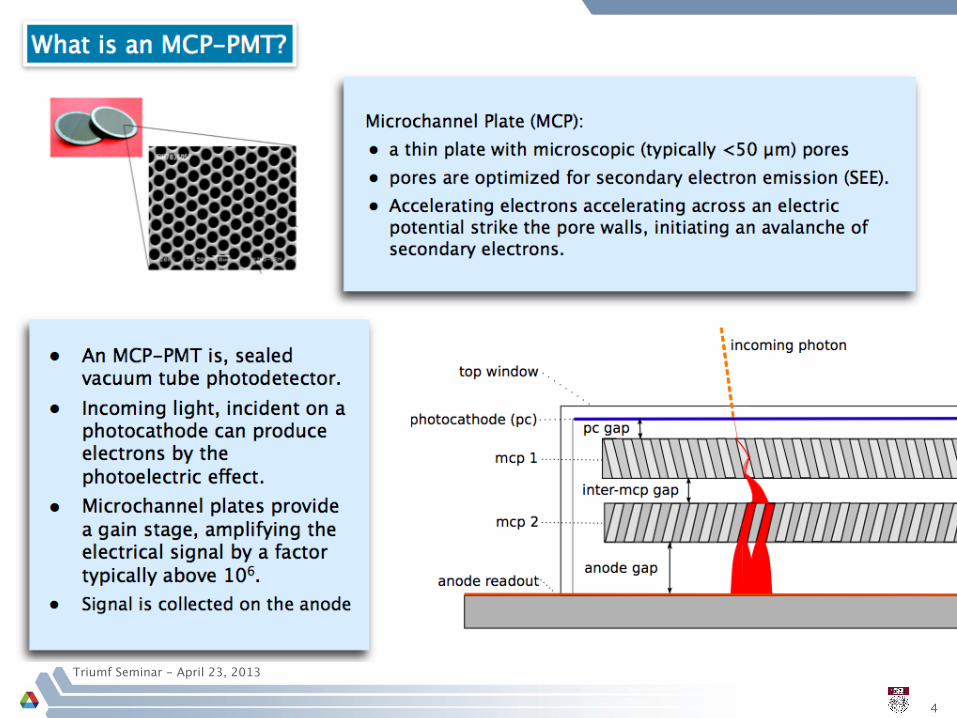
What is an MCP
Triumf Seminar - April 23, 2013
Snowmass - August, 2013
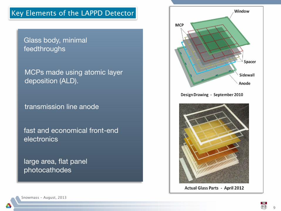
Glass body, minimal feedthroughs
transmission line anode
fast and economical front-end electronics
large area, flat panel photocathodes
MCPs made using atomic layer deposition (ALD).
9
Key Elements of the LAPPD Detector

Snowmass - August, 2013
106
The Wonders of Pure Materials
Lifetime of latest generation Microchannel Plate PMT’s
�
A. Britting
1, W. Eyrich
1, A. Lehmann
† 1, F. Uhlig
1, and PANDA Cherenkov group
1Physikalisches Institut IV, Universitat Erlangen-Nurnberg, Erwin-Rommel-Str. 1, D-91058 Erlangen
Introduction
Multi-anode microchannel plate (MCP) PMTs have su-perior performance characteristics compared to standarddynode PMTs: they are very compact, they can be oper-ated in magnetic field environments up to 2 Tesla, and theyshow an excellent time resolution of <50 ps. These are themain reasons why MCP-PMTs are the preferred option forboth PANDA DIRCs.
Over the past few years our group has studied the char-acteristics of many of the commercially available typesof MCP-PMTs. During this time their two main draw-backs, rate capability and lifetime, were improved step bystep [1, 2]. Still, until recently the lifetime of these de-vices was not enough for the anticipated period of opera-tion inside PANDA of � 10 years. At the focal plane ofthe PANDA DIRCs photon rates up to � 5 MHz/cm2 areexpected which may add up to an integrated anode chargeof several C/cm2/year. During 2010, new models of MCP-PMTs became available whose lifetimes are getting closeto the requirement of � 5 C/cm2 for the barrel DIRC.
Techniques to Increase the Lifetime
A diminishing quantum efficiency (QE) of the photocathode (PC) is the primary cause for the aging of MCP-PMTs. The 3 main manufacturers of MCP-PMTs applydifferent techniques to prolong the lifetime. Hamamatsu’sapproach for their R10754X is a very thin protection layerof aluminium oxide between the 1st and the 2nd channelplate to stop feedback ions from hitting the PC. BINP cre-ates an improved vacuum inside the tube and the MCP sur-faces are scrubbed with electrons. In addition the PC istreated in vapors of antimony and cesium which seems tosignificantly improve its hardness against feedback ions.
A quite different technique is applied in the latest MCP-PMT prototype (XP85112) of Photonis. To reduce the out-gassing of the lead glass MCPs, these are coated with athin layer of a secondary electron emissive material directlyon the pores using an atomic layer deposition (ALD) tech-nique. Currently this seems to be the most promising ap-proach to increase the lifetime of MCP-PMTs.
Results
Our group is presently in the process of simultaneouslymeasuring the lifetimes of several types of MCP-PMTs ofthe 3 manufacturers listed above. The illumination of alltubes is done in parallel with an intensity comparable to
� Work supported by BMBF and GSI† [email protected]
that expected inside PANDA. In time intervals of severaldays the quantum efficiencies are measured as a functionof the wavelength; in addition, every several weeks a scanof the position dependence of the QE across the PC is done.
The current status is shown in Fig. 1, where the QE ofall investigated MCP-PMTs is plotted as a function of theintegrated anode charge. Obviously all of the latest modelsshow a very significant improvement in the lifetime.
In Fig. 2 the same plots are shown for different wave-lengths. At least for the XP85112 the QE behaves the samefor all wavelengths still at 1 C/cm2. This is different to for-mer observations where aging caused the QE to drop fasterfor longer wavelengths than for shorter ones [3]. We seethis as a positive sign that the tube will stand more charge.
]2integrated anode charge [mC/cm0 200 400 600 800 1000
QE
[%]
0
5
10
15
20
25m)µHam. R10754-01-M16 (JT0117 - 10
m)µHam. R10754-01-M16 (JT0117 - 10m)µPhot. XP85112/A1-HGL-9001223 (10
m)µBINP 3548 (7m)µPhot. XP85112/A1-9000897 (10
m)µPhot. XP85012-9000296 (25m)µBINP 82 (6
Lifetime of several MCP-PMTs
Figure 1: QE at 400 nm for old (open) and new generation(solid dots) MCP-PMTs as function of the anode charge.
]2integrated anode charge [mC/cm0 200 400 600 800 1000
rela
tive
QE
0.8
0.9
1.0
1.1
300 nm350 nm400 nm450 nm500 nm550 nm
Hamamatsu R10754X-M16
]2integrated anode charge [mC/cm0 200 400 600 800 1000
rela
tive
QE
0.8
0.9
1.0
1.1
300 nm350 nm400 nm450 nm500 nm550 nm
Photonis XP85112
Figure 2: Relative QE for different wavelengths normalizedto 300 nm for the XP85112 and R10754X MCP-PMTs.
References
[1] A. Lehmann et al., GSI Scientific Report 2010, p. 106.[2] A. Lehmann et al., Nucl. Instr. and Meth. A639 (2011) 144.[3] A. Lehmann et al., GSI Scientific Report 2009, p. 7.
PHN-HSD-PANDA-06 GSI SCIENTIFIC REPORT 2011
126
Lifetime of latest generation Microchannel Plate PMT’sA. Britting, W. Eyrich, A. Lehmann†, F. Uhlig, and PANDA Cherenkov group
4+<:(%.*?<'6+-(%-':69'A+RC,:%KC9%Ia%
WNS,*/%.,-%KC9%A.3=)9C+,-%(J(,6:/%
85(9(%*.>%A(%(E3(::%A.3=)9C+,-%-+(%
6C%-(6(3RC,%CK%'C,%?+*?%(J(,6:"%
WPPP%:(3%A.3=)9C+,-/%NMT%3C+,6:/%.6%O"S%E%WPT%
).',/%OTPPJ%6C6.</%X'65%NPPJ%C,%.,C-("%
1.3=)9C+,-%9.6(%':%%P"PMM%(J(,6:%3*\O%:(3\W"%%
0
5000
1 104
1.5 104
2 104
2.5 104
3 104
3.5 104
0
10
20
30
40
50
0 2 106 4 106 6 106 8 106 1 107
2600v
2600v bkg
UV
coun
ts (1
00 s
ec)
Background Counts (1000 sec)
Gain
2L4%A.3=%6C%A.3=%?.'9/%OPd*%?C9(:/%gh%A'.:/%TPkW%GZ-/%.35'(J(:%oP"W%(J(,6:%3*\O%:(3\W"%%
Typical MCP behavior- long scrub-times
Measured ANL ALD-MCP behavior
11
LAPPD concept
5
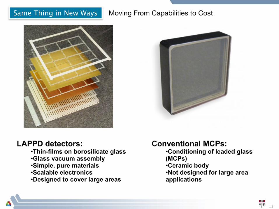
LAPPD detectors:•Thin-films on borosilicate glass•Glass vacuum assembly•Simple, pure materials•Scalable electronics•Designed to cover large areas
Conventional MCPs:•Conditioning of leaded glass (MCPs)•Ceramic body•Not designed for large area applications
Same Thing in New Ways Moving From Capabilities to Cost
Snowmass - August, 2013
126
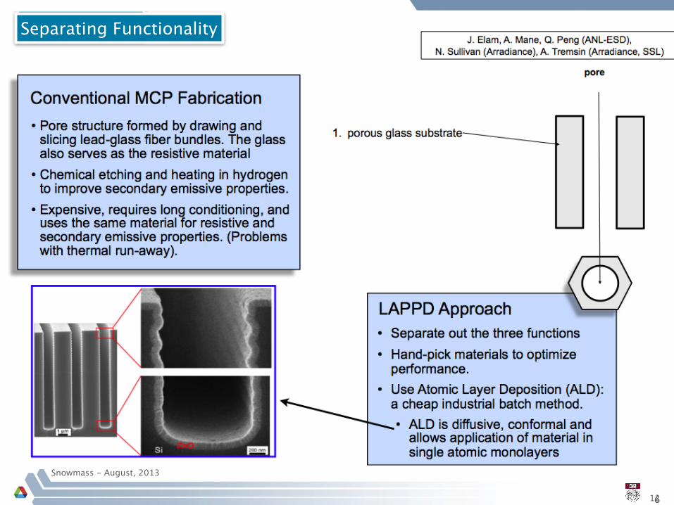
Separating Functionality
Snowmass - August, 2013
137
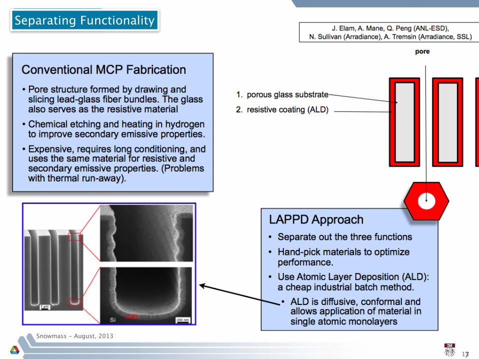
Separating Functionality

Snowmass - August, 2013
148
Separating Functionality

Snowmass - August, 2013
159
Separating Functionality
Snowmass - August, 2013
169
Separating Functionality
05/05/10 RICH 2010
LAPPD Collaboration: Large Area Picosecond Photodetectors
Photocathode FabricationTwo parallel efforts:
• Work at UC Berkeley (SSL) to scale conventional multi-alkali photocathodes to large-area, flat geometries.
K. Broughton, E. Indacochea (UIC), X. Li, R. Dowdy (UIUC), B. Adams, M. Chollet, Z. Insepov, S. Jokela, A. Mane, Q. Peng, T. Prolier, M. Wetstein, I. Veryovkin, Z. Yusof, A. Zinovov (ANL), O. Siegmund, J. McPhate, S. Jelensky, A. S. Tremsin, J. V. Vllerga (Berkeley, SSL), V. Ivonov (Muons Inc)
• Work at Argonne to develop a fabrication and testing chamber
• to complement Berkeley’s multi-alkali work
• further the fundamental understanding of photocathode materials
• look into novel photocathode designs (advanced materials, nano-structures...)
Possible long-term photocathode center at ANL
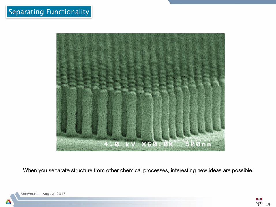
When you separate structure from other chemical processes, interesting new ideas are possible.

Snowmass - August, 2013
Material Science as Science
17
Photocathodes are an example of a technology, often taken for granted, where there is a lot of room to understand the basic underlying physics.
Material scientists and HEP folks are making strides in understanding the basic materials and optimizing them for ultra-high QEs.
See, for example:
Second Workshop on Photocathodes - U Chicago
https://psec.uchicago.edu/workshops/2nd_photocathode_conference/

0
200
400
600
800
1000
9.5 10 10.5 11
30v Gap85v Gap145v Gap257v GapHigh S/N Laser
Cou
nts
Time (ns)
212ps FWHM230ps FWHM
480ps FWHM286ps FWHM
64 ps FWHM (27 ps rms)
0
5
10
15
20
25
30
350 400 450 500 550 600 650
Tube#1 QE
7-22-13 (Hot)7-23-13 (Cold)7-26-13
Qua
ntum
Effi
cien
cy (%
)
Wavelength (nm)
Snowmass - August, 2013
Postscript/News Flash!
18
• First complete LAPPD (with photocathode) has been sealed at Berkeley SSL
• Will be brought to air, any day now...possibly before Snowmass ends.0.00
5.00
10.00
15.00
20.00
25.00
350 400 450 500 550 600 650 700
QE
Wavelength (nm)
8" Cathode Tube#1- 2013-07-23 cold 9:&&;%<$15$3%7$'14,)%!"#$%/=%
Y.K#@;(<*A#0%&'#<;#>-.=-%00#
)*+%#2<K5#2<;(.2#5.K#<;(<*A#0%&'#/.A>'%K%(#N.A>'%K%(#/&K5.(%?#(&-D#+-.2;#05&(%(#

Snowmass - August, 2013
Importance of Cross-pollination
19
Reaching out to other communities can produce an unstoppable force.

Snowmass - August, 2013
Importance of Cross-pollination
20
Any questions?