atomic-levelstructureanddeformationinmetallic glasses · structure-to ... and wrote the manuscript...
TRANSCRIPT

Atomic-level structure and deformation in metallicglasses
Thesis byDavid Z. Chen
In Partial Fulfillment of the Requirements for thedegree of
Doctor of Philosophy
CALIFORNIA INSTITUTE OF TECHNOLOGYPasadena, California
2016Defended May 3, 2016

ii
© 2016
David Z. ChenORCID: 0000-0001-5732-5015
All rights reserved

iii
ACKNOWLEDGEMENTS
Time is a fickle thing, but it sure flies when you are having fun. Eight years agoI walked into Prof. Rodney Ruoff’s lab at the University of Texas at Austin asa bright-eyed undergraduate researcher. His postdoc, Dr. Weiwei Cai taught meabout electrical measurements, ultra-high vacuum systems, evaporative deposition,and I was in awe at how precise and fascinating everything was. It was like walkingonto the set of a new Spiderman movie, but better - because it was real. I lovescience for its people, who always have the time to share their knowledge with youand who are fueled by a passion in their hearts for finding out natural truths. Onelittle-known fact about Caltech is that its motto is "The truth will make you free."This statement resonates with me as a scientist and as a human being, and I resonatewith others who also feel drawn towards the truth. There are many, many peoplewho have helped me along the way, and I have done my best to help others as well(the circle of science, so to speak). I would not have gotten this far without myfriends, colleagues, and family. Mom and dad, thank you for your unconditionalsupport and love. My close friends (you know who you are), thank you all for thelaughs and good times - you are the catalyst for getting me out of rough slumps.My colleagues and lab mates (you know who you are), thank you for being true toyourselves - you are the reason I love science. Finally, my advisor Julia, thank youfor all of your support and mentorship. I admire your boundless energy - you are aninfinite reservoir of heat for our engines of research.

iv
ABSTRACT
Metallic glasses (MGs) are a relatively new class of materials discovered in 1960and lauded for its high strengths and superior elastic properties. Three major obsta-cles prevent their widespread use as engineering materials for nanotechnology andindustry: 1) their lack of plasticity mechanisms for deformation beyond the elasticlimit, 2) their disordered atomic structure, which prevents effective study of theirstructure-to-property relationships, and 3) their poor glass forming ability, whichlimits bulk metallic glasses to sizes on the order of centimeters. We focused onunderstanding the first two major challenges by observing the mechanical propertiesof nanoscale metallic glasses in order to gain insight into its atomic-level structureand deformation mechanisms. We found that anomalous stable plastic flow emergesin room-temperature MGs at the nanoscale in wires as little as ∼100 nanometerswide regardless of fabrication route (ion-irradiated or not). To circumvent exper-imental challenges in characterizing the atomic-level structure, extensive molec-ular dynamics simulations were conducted using approximated (embedded atommethod) potentials to probe the underlying processes that give rise to plasticity innanowires. Simulated results showed that mechanisms of relaxation via the samplefree surfaces contribute to tensile ductility in these nanowires. Continuingwith char-acterizing nanoscale properties, we studied the fracture properties of nano-notchedMG nanowires and the compressive response ofMG nanolattices at cryogenic (∼130K) temperatures. We learned from these experiments that nanowires are sensitiveto flaws when the (amorphous) microstructure does not contribute stress concentra-tions, and that nano-architected structures with MG nanoribbons are brittle at lowtemperatures except when elastic shell buckling mechanisms dominate at low ribbonthicknesses ( 20 nm), which instead gives rise to fully recoverable nanostructures re-gardless of temperature. Finally, motivated by understanding structure-to-propertyrelationships in MGs, we studied the disordered atomic structure using a combi-nation of in-situ X-ray tomography and X-ray diffraction in a diamond anvil celland molecular dynamics simulations. Synchrotron X-ray experiments showed theprogression of the atomic-level structure (in momentum space) and macroscale vol-ume under increasing hydrostatic pressures. Corresponding simulations providedinformation on the real space structure, and we found that the samples displayedfractal scaling (rd ∝ V , d < 3) at short length scales (< ∼8 Å), and exhibited acrossover to a homogeneous scaling (d = 3) at long length scales. We examined

v
this underlying fractal structure of MGs with parallels to percolation clusters anddiscuss the implications of this structural analogy to MG properties and the glasstransition phenomenon.

vi
PUBLISHED CONTENT AND CONTRIBUTIONS
(1) Chen, D. Z.; Jang, D.; Guan, K. M.; An, Q.; W. A. Goddard, I.; Greer, J. R.Nano Letters 2013, 13, DOI: 10.1021/nl402384r,D.Z.C. performed in situ tensile experiments, EDX,XRD, and SEManalysis,fabricated samples using FIB, developed the electroplating process, preparedthe data, and wrote the manuscript with input from D.J., Q.A., K.M.G.,W.A.G., and J.R.G.
(2) Gu, X. W.; Jafary-Zadeh, M.; Chen, D. Z.; Wu, Z.; Zhang, Y.-W.; Srolovitz,D. J.; Greer, J. R. Nano Letters 2014, 14, DOI: 10.1021/nl5027869,D.Z.C. fabricated notched samples and assisted in sample characterizationand data interpretation.
(3) Chen, D. Z.; Gu, X.W.; An, Q.; Goddard,W. A.; Greer, J. R.Applied PhysicsLetters 2015, 106 061903, DOI: 10.1063/1.4907773,D.Z.C. fabricated samples, assisted in conducting experiments and perform-ing simulations, interpreted the results, and wrote the manuscript with inputfrom all authors.
(4) Gallant, B. M.; Gu, X. W.; Chen, D. Z.; Greer, J. R.; Lewis, N. S. ACS Nano2015, 9, DOI: 10.1021/acsnano.5b00468,D.Z.C. assisted in tensile tests and interpretation of data.
(5) Lee, S.-W.; Jafary-Zadeh, M.; Chen, D. Z.; Zhang, Y.-W.; Greer, J. R. NanoLetters 2015, 15, DOI: 10.1021/acs.nanolett.5b01034,D.Z.C. assisted in sample fabrication, characterization, interpretation ofresults, and manuscript preparation.
(6) Adibi, S.; Branicio, P. S.; Liontas, R.; Chen, D. Z.; Greer, J. R.; Srolovitz,D. J.; Joshi, S. P. Extreme Mechanics Letters 2015, 5, DOI: 10.1016/j.eml.2015.08.004,D.Z.C. assisted in interpretation of results and preparation of themanuscript.
(7) Chen, D. Z.; Shi, C. Y.; An, Q.; Zeng, Q.; Mao, W. L.; Goddard, W. A.;Greer, J. R. Science 2015, 349, DOI: 10.1126/science.aab1233,D.Z.C. fabricated samples, assisted in X-ray tomography and molecular dy-namics simulations. D.Z.C. interpreted the results and wrote the manuscriptwith input from all authors.

vii
TABLE OF CONTENTS
Acknowledgements . . . . . . . . . . . . . . . . . . . . . . . . . . . . . . . iiiAbstract . . . . . . . . . . . . . . . . . . . . . . . . . . . . . . . . . . . . . ivPublished Content and Contributions . . . . . . . . . . . . . . . . . . . . . . viTable of Contents . . . . . . . . . . . . . . . . . . . . . . . . . . . . . . . . viiList of Illustrations . . . . . . . . . . . . . . . . . . . . . . . . . . . . . . . ixList of Tables . . . . . . . . . . . . . . . . . . . . . . . . . . . . . . . . . . xiNomenclature . . . . . . . . . . . . . . . . . . . . . . . . . . . . . . . . . . xiiChapter I: Introduction . . . . . . . . . . . . . . . . . . . . . . . . . . . . . 1
1.1 Background and Brief Outline . . . . . . . . . . . . . . . . . . . . . 2Chapter II: Origin of Size-Effect in Ductile Nano-sized Metallic Glasses . . . 4
2.1 Electroplated Ni-P metallic glass nanowires . . . . . . . . . . . . . . 62.2 In-situ tensile experiments . . . . . . . . . . . . . . . . . . . . . . . 72.3 Discussion of experimental findings . . . . . . . . . . . . . . . . . . 102.4 Molecular dynamics of Ni80Al20 . . . . . . . . . . . . . . . . . . . 122.5 Conclusions . . . . . . . . . . . . . . . . . . . . . . . . . . . . . . 15
Chapter III: Work Hardening in a Metallic Glass . . . . . . . . . . . . . . . . 163.1 Electroplating smaller samples . . . . . . . . . . . . . . . . . . . . 163.2 Sample characterization and testing . . . . . . . . . . . . . . . . . . 173.3 Free surface relaxation pathways . . . . . . . . . . . . . . . . . . . 183.4 Estimation of characteristic timescale for relaxation . . . . . . . . . 233.5 Discussion of work hardening and implications . . . . . . . . . . . . 24
Chapter IV: Fracture of nano-notched wires . . . . . . . . . . . . . . . . . . 264.1 Fabrication of notched nanowires . . . . . . . . . . . . . . . . . . . 274.2 SEM and TEM characterization . . . . . . . . . . . . . . . . . . . . 284.3 In-situ mechanical tests . . . . . . . . . . . . . . . . . . . . . . . . 294.4 Molecular dynamics simulations . . . . . . . . . . . . . . . . . . . . 314.5 Discussion of results . . . . . . . . . . . . . . . . . . . . . . . . . . 324.6 Summary . . . . . . . . . . . . . . . . . . . . . . . . . . . . . . . . 364.7 Low temperature behavior of metallic glass lattices . . . . . . . . . . 36
From Property-to-Structure, to Structure-to-Property . . . . . . . . . . . . . 51Chapter V: Dimensionality of the Atomic-Level Structure . . . . . . . . . . . 52
5.1 Fractal scaling in metallic glasses . . . . . . . . . . . . . . . . . . . 535.2 Real space estimates of local dimension . . . . . . . . . . . . . . . . 545.3 Percolation models to describe dimensional crossover . . . . . . . . 555.4 Discussion of implications . . . . . . . . . . . . . . . . . . . . . . . 58
Chapter VI: Comparison of Structural Dimensionality in Liquids and Glasses 606.1 Dimension and crossover . . . . . . . . . . . . . . . . . . . . . . . 626.2 Comparison to Copper and grid analysis . . . . . . . . . . . . . . . 656.3 Discussion and summary . . . . . . . . . . . . . . . . . . . . . . . 66

viii
Chapter VII: Discussion and comments on the results and future directions . . 70Bibliography . . . . . . . . . . . . . . . . . . . . . . . . . . . . . . . . . . 73Appendix A: Methods and supporting information . . . . . . . . . . . . . . . 83
A.1 Supporting methods . . . . . . . . . . . . . . . . . . . . . . . . . . 84A.2 Supporting discussion . . . . . . . . . . . . . . . . . . . . . . . . . 88

ix
LIST OF ILLUSTRATIONS
Number Page2.1 Scope of fabrication methods for nano-sized MG specimen . . . . . . 52.2 Microstructure characterization of fabricated MG samples . . . . . . 82.3 Mechanical behavior of EP and FIB samples under tension . . . . . . 102.4 Stress-strain curves of EP and FIB Ni-P samples in MD . . . . . . . 133.1 Electroplating smaller Ni-P samples . . . . . . . . . . . . . . . . . . 173.2 Electron micrographs and stress strain data showing work hardening
behavior . . . . . . . . . . . . . . . . . . . . . . . . . . . . . . . . 193.3 Comparison of mechanical response in differently-sized samples . . . 203.4 Tracking volume evolution during deformation in MD . . . . . . . . 224.1 Fabrication and characterization of notched nanowires . . . . . . . . 284.2 In-situ tensile tests on notched nanowires . . . . . . . . . . . . . . . 304.3 Molecular dynamics simulations of notched nanowires . . . . . . . . 334.4 Detailed view of the deformation in notched nanowires . . . . . . . . 344.5 Stress triaxiality in notched nanowires . . . . . . . . . . . . . . . . . 354.6 SEM images of MG nanolattices . . . . . . . . . . . . . . . . . . . . 394.7 Engineering stress-strain curve of MG nanolattices . . . . . . . . . . 404.8 Snapshots of in situ deformation of MG nanolattices with the wall
thicknesses of 20 nm . . . . . . . . . . . . . . . . . . . . . . . . . . 424.9 MD simulations of nanolattices at various temperatures . . . . . . . . 44
4.10 MG nanolattice deformation map in the temperature-thickness space . 505.1 In-situ diffraction and volume results . . . . . . . . . . . . . . . . . 545.2 Dimensionality crossover in simulations . . . . . . . . . . . . . . . . 555.3 Concepts in fractals and percolation . . . . . . . . . . . . . . . . . . 565.4 Simulated properties during supercooling . . . . . . . . . . . . . . . 586.1 Crossover and features of the RDF . . . . . . . . . . . . . . . . . . . 636.2 Local dimensions in metallic glasses . . . . . . . . . . . . . . . . . . 646.3 Local dimensions in metallic liquids . . . . . . . . . . . . . . . . . . 656.4 Comparison of crossovers in pure Cu systems using discrete and
continuous counting methods. . . . . . . . . . . . . . . . . . . . . . 67A.1 Average Young’s moduli for FIB and EP samples across ten indepen-
dent specimens . . . . . . . . . . . . . . . . . . . . . . . . . . . . . 83

x
A.2 Graph depicting the d2 versus d3 scaling argument for surface energy 83A.3 Diagram for the generation of high potential energy atoms from ion
irradiation . . . . . . . . . . . . . . . . . . . . . . . . . . . . . . . 84

xi
LIST OF TABLES
Number Page2.1 Compositions and geometries of FIBed samples . . . . . . . . . . . 62.2 Compositions and geometries of EPed samples . . . . . . . . . . . . 6A.1 Electroplating conditions employed for plating both our Ni-P film
(FIB) and templated (EP) specimen. . . . . . . . . . . . . . . . . . . 84

xii
NOMENCLATURE
∆ε strain within the shear band volume p. 47
∆G activation barrier for free volume jump p. 23
Γ shear band energy p. 46
γ geometrical factor taken to be 0.5 p. 23
λ average free volume jump length for a unit of free volume p. 23
ν Poisson’s ratio p. 48
Ω average atomic volume p. 23
φ packing fraction p. 23
φc critical volume fraction (percolation threshold in continuum) p. 56
φ j jamming packing fraction (point j) p. 59
ρ bulk density p. 23
σy yield strength p. 46
τ shear stress p. 23
ξ correlation length in percolation models p. 56
d dimensionality p. 53
f D Debye frequency p. 23
Ld characteristic diffusion length p. 24
pc percolation threshold p. 55
ravg metallic radius of a single element of interest (one half of the roomtemperature lattice parameter), or average of elements of inter-est p. 62
ris outer radius of the ith coordination shell in the real space RDF p. 62
v∗ average critical free volume necessary for a jump p. 23
v f average free volume p. 23
A aspect ratio of the sample p. 46
a major radius of elliptical cross section p. 48

xiii
c speed of sound p. 23
D diffusion coefficient p. 23
E Young’s modulus p. 46
K bulk modulus p. 23
k Boltzmann constant p. 23
L length of cylindrical tube p. 48
M mass p. 53
p occupancy probability in percolation p. 55
qi ith peak in momentum transfer (x-ray diffraction) data p. 53
r distance in real space p. 53
T temperature p. 23
t layer thickness of cylinder p. 48
Tg glass transition temperature p. 58

1
C h a p t e r 1
INTRODUCTION
At the University of Texas at Austin, I worked primarily on two topics, graphene(under Rodney Ruoff) and polymer nanocomposites (under Joseph Koo). One thingthat struck me was the stark difference between our approach for understandingordered and homogeneous materials (e.g. graphene) and disordered and hetero-geneous materials (e.g. polymer nanocomposites). For graphene, the structure ofthe material is easy to visualize - carbon atoms arranged in a honeycomb-shapedsheet. Polymer nanocomposites, on the other hand, are a mess - all we know isthat the nanomaterials are embedded in a polymer matrix and its concentration,but not even something simple like how well-mixed it is (e.g. average spacing ofsolute). We characterize ordered systems at the fundamental building-block level,e.g. via crystal structures, and such descriptions are rich and useful for our under-standing of the structure. We characterize disordered systems at the system level,e.g. concentrations of solutes and phases, or composition of the overall sample.The fundamental constituents can no longer fully describe the disordered systembecause the arrangement, or topology of those constituents are an integral part of theoverall system structure. With isolated graphene sheets, we can apply an approachfrom fundamental physics. However, if you simply mix those sheets into a polymermatrix, the problem becomes indefinitely more complex. Working with these het-erogeneous, disordered materials as an undergraduate researcher, I often felt like anengineer, applying different amounts of additives and characterizing the compositeto see how the properties changed. Somewhere on the spectrum between individualgraphene sheets and graphene sheets randomly dispersed in an amorphous matrix,we lose our ability to fully describe the structure. As scientists, we seem to have adiscomfort with disorder, but this discomfort is not a two-way street, as disorderedmaterials often have very repeatable properties. Make two nanocomposites in thesame way, and they will have the same properties regardless of the local coordinatesand orientations of each graphene flake. There is an underlying regularity to thedisordered mess.
Our discomfort with disorder is illustrated by our choice of nomenclature for non-crystalline materials, which we lump together to call amorphous, a word withconnotations of structureless, formless, and unclassifiable. Asmaterial scientists, we
2
often talk about understanding structure-to-property relationships in materials. Howcan we understand the structure and properties of such disordered and "formless"materials? It is instructive to study a material that has arguably the most disorder,metallic glasses, which are disordered at the atomic level. In this dissertationwe will explore the peculiar properties of metallic glasses at the nanoscale andattempt to understand those properties by inferring changes/differences in the stateof the atomic-level structure. These differences are extremely difficult to captureexperimentally, as amorphous materials always appear amorphous even though theirproperties (and structures) depend greatly on their fabrication histories. Structuraldifferences are hard to characterize in glasses, but their overall property differencesare not. Therefore, the material scientist’s approach of structural understandingbrings property understanding is reversed for amorphous materials. In many cases,one must start with the properties and infer the structural details. Towards theend of this dissertation we will attempt to characterize the atomic-level structureof these disordered metallic glasses by looking at their local dimensionality. Wewill utilize the percolation framework as a potential way for understanding howdifferences in atomic structure arise in metallic glasses and how we may beginto understand and characterize them, thereby correcting the order of structure-to-property relationships.
1.1 Background and Brief OutlineAmorphous metals, or metallic glasses, were first discovered in 1960 by the grad-uate students of Pol Duwez, who was, incidentally, the advisor of two memberson my Thesis Committee (William A. Goddard and William L. Johnson). Duwezand his students alloyed Au with Si and studied its structure after splat quenching,and they were surprised to find that at certain amounts of Si, the structure was notcrystalline.[1] Since their discovery, metallic glasses have garnered a lot of atten-tion as potential structural materials. They have high strengths, high elastic limits,corrosion resistance, and great processability. However, their lack of mechanismsfor stable plastic flow is a major Achilles heel. At room temperatures, a catastrophicshear band propagates at the elastic limit - the amount of useful plasticity is effec-tively zero. I will start off by discussing our experiments on nano-sized metallicglasses, which show that metallic glasses have intrinsic mechanisms for plastic flowat the nanoscale. Then I will discuss the atomistic origins of this tensile ductilityin nano-wires using molecular dynamics simulations. The challenges that arisein developing intuition on the subtle structural differences that give rise to these

3
nanoscale phenomena will motivate our discussion on the atomic-level structure inmetallic glasses.

4
C h a p t e r 2
ORIGIN OF SIZE-EFFECT IN DUCTILE NANO-SIZEDMETALLIC GLASSES
Substantial research has been directed at alleviating the brittleness ofmetallic glasses(MGs) under tension, where deformation is typically marked by elastic loadingfollowed by catastrophic failure via shear localization within a narrow region calleda shear band.[2] Some such toughening efforts make use of various heterostructuresand composites, such as the inclusion of dendritic phases, macro-pores, and otherobstacles to impede shear band propagation.[3–5] These methods are effective indelaying brittle failure, but intrinsic mechanisms for sustained plasticity in MGsare not activated at room temperatures. An assumption that many literature reportsmake on bulk monolithic metallic glasses is that the only plasticity carriers areshear bands. Recent in-situ nanomechanical experiments on MGs have shown a"brittle-to-ductile" transition, which emerges in ∼100 nm-sized MG wires/pillarsfabricated using Focused Ion Beam (FIB) milling and subjected to compression[6–8] and tension[9, 10]. These observations suggest a possible mechanism for intrinsicductility in metallic glasses at room temperatures, one that may not rely on impedingshear band propagation.1
The origin of this so-called brittle-to-ductile transition is unclear in part because theexperimental results are inconsistent, with some literature reporting this transition tooccur at 400 nm[8], 200 nm[6], and 100 nm[7, 9, 10] or not seeing any suppressionof catastrophic failure even for samples of 150-300 nm[11–14]. Most of the existingliterature on nano-mechanical deformation of individual metallic glass nano struc-tures describes experiments on samples fabricated using a focused ion beam (FIB).Thismilling technique irradiates the sample surfacewith a relatively high-energy ionbeam, which can potentially lead to a modification of the local atomic arrangementsor even to surface crystallization.[15–17] Molecular dynamics (MD) simulations byXiao, et al. revealed that ion bombardments suppressed shear band formation in106.4eV-irradiated Zr-based metallic glass nanowires (7.8 nm in diameter and 17.7nm in length).[18] An alternate synthesis of individual nano-sized metallic glassessuitable for mechanical testing is necessary to ascertain whether the size-induced
1Parts of this chapter are published online at DOI: 10.1021/nl402384r

5
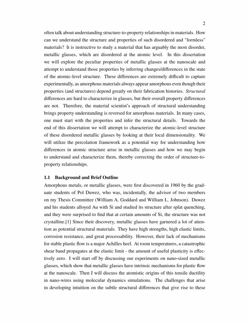
brittle-to-ductile transition is a real physical phenomenon and to shed further lighton understanding the deformation mechanisms in metallic glasses at small scales.To date, there has been a paucity of “FIB-less” fabrication methods to produce indi-vidual nano-scale metallic glass specimens for nanomechanical testing. Verticallyaligned cylindrical nanowires have been synthesized by nanomoulding from bulksamples[14, 19] (Fig. 1a) and thin metallic glass films have been electroplated ontoindium-tin-oxide-coated (ITO) glass substrates[20] (Fig. 1b) and deposited usingradio frequency magnetron sputtering[21]. None of these methods is well-suitedfor measuring the mechanical properties of individual nano-sized samples. Se-lectively removing individual moulded nanowires is one possibility for producingsuch samples, and tensile experiments on removed Pt57.5Cu14.7Ni5.3P22.5 nanowiresrevealed that for samples ranging from ∼100-150nm in diameters and ∼1-3µm ingauge lengths, ion irradiation was able to induce a brittle-to-ductile transition, whilesubsequent annealing reversed it.[14]
Figure 2.1: Scope of fabrication methods for nano-sized MG specimen. a) Tem-plated metallic glass nanowires fabricated without the use of ion beam irradiation.b) Electroplating method for creating thin metallic glass coatings and films on sub-strates. An appropriate electrolyte solution is provided with a favorable currentdensity, which drives the ions toward the cathode/substrate. Magnetron sputteringis also possible c) Focused ion beam milling of a bulk metallic glass into nano-scaledimensions for nanomechanical testing. Both compressive and tensile samples canbe made in this fashion. d) Templated electroplating procedure used in this work,which utilizes a spin-coated PMMA to act as a mask, isolating the conductive pathbetween anode and cathode at select pillar-shaped holes. Tensile and compressivesamples can be fabricated by using this technique.

6
2.1 Electroplated Ni-P metallic glass nanowiresWe fabricated Ni1−xPx metallic glass nano-tensile samples with ∼100nm- and500nm- diameters and ∼650nm- and 2µm− heights. This synthesis was carriedout by electroplating the metallic glass into a Polymethylmethacrylate (PMMA)template, which was spin-coated onto a pre-sputtered Au seed layer on a Si chipand patterned via e-beam lithography (Fig. 2.1d). In addition, a 2µm−thick filmwas separately electroplated directly onto another substrate by following the sameprocedure, and nano-tensile samples with identical geometries were FIB-carved intothe film. The two sets of samples - electroplated and FIB-carved - were virtuallyidentical to each other, both in composition and geometry (see Table 2.1 & 2.2 forchemical composition analysis and Figure 2.3 for the SEM images of representativesamples). Experiments on these samples allowed for a direct comparison betweenthe mechanical responses of otherwise the same metallic glass nano structures withirradiated vs. as-fabricated surface states. A Ni-P system was chosen because itlends itself well to electroplating. NiP metallic glasses may have different shortrange order (SRO) compared with the more common binary glass, CuZr, which hasmore metallic-like bonding (see Appendix discussion).[22] Tensile results revealedcatastrophic failure in 500nm-diameter samples and post-elastic deformability in100nm-diameter samples fabricated by both techniques. The extent of tensile duc-tility was nearly a factor of three greater in FIB samples, which suggests that aless relaxed (irradiated) surface state may facilitate homogeneous plastic flow viaactivation of numerous diffuse shear bands.
Focused ion beam (FIB) milledComp. (wt%) Diameter (nm) Length (nm)P - 14.0 Ni - 86.0 93.4 ± 7.77 598.2 ± 21.97
Table 2.1: Compositions and geometries of FIBed samples
Template-electroplated (EP)Comp. (wt%) Diameter (nm) Length (nm)P - 14.9 Ni - 85.1 104.8 ± 6.46 633.0 ± 76.57
Table 2.2: Compositions and geometries of EPed samples
Figure 2.2 shows an array of electroplated pillars (Fig. 2.2(a)), tensile (Fig. 2.2(b))and compressive (Fig. 2.2(c)) samples, dark-field transmission electron microscopy(TEM) image (Fig. 2.2(d)), X-ray diffraction (XRD) pattern (Fig. 2.2(e)), andenergy-dispersive X-ray spectrum (EDX) (Fig. 2.2(f)). TEM and EDX analyses

7
were performed on a representative nano-pillar, while the thin metallic glass filmwas characterized by XRD and EDX. XRD was not performed on the nanopillarsbecause they are smaller than the x-ray beam spot size. The feature-less darkfield TEM image and the corresponding diffuse-ring electron diffraction patternof a 500 nm electroplated nano-tensile sample (Fig. 2.1d) confirm the amorphousmicrostructure of these electroplated alloys. The EDS analysis (Fig. 2.1f) of relativeconcentrations of Ni and P revealed that the concentrations of phosphorous, ∼14.9wt% in the nano-pillars and ∼14 wt% in the thin film, were virtually identical. Thesubstantial amount of carbon (∼4.5 wt%) and oxygen (∼4 wt%) on the surface ofthe electroplated samples was likely a result of the residual organic solvents usedto remove the PMMA. The FIB-machined samples also contained a considerableamount of carbon (∼3.4 wt%) and oxygen (∼1.2 wt%), typical of most metallicsurfaces exposed to air. The effect of these surface impurities on the mechanicalproperties is likely negligible because they do not form continuous layers and henceare not able to bear any load (see Appendix for additional discussion on surfacecontamination). XRD spectra of the electroplated thin film, shown in Figure 2.2e,reveals the presence of three strong peaks: two for the Si substrate (100) and theseed Au layer ([420]). The broad peak at 2θ = 20 stems from the glass slide ontowhich the sample was mounted. No known peaks for nickel (2θ = ∼45, Ni [111])were observed, instead a broad weak peak (indicated by the blue arrow) was presentnear 2θ of 45. These observations imply that the electroplated Ni-P metallic alloywas amorphous, consistent with reported literature.[23]
2.2 In-situ tensile experimentsFigure 2.3 shows tensile engineering stress vs. engineering strain data for typical100nm-diameter samples fabricated by both techniques as well as the progressionsof the corresponding in-situ SEM images during each experiment, which coincidewith the same letter-labeled points in the data. The strain was calculated fromthe displacement using the frames from the in-situ SEM video rather than thedisplacement signal from the nanoindenter, a method which has been shown tobe more accurate in nano-mechanical experiments[10, 24, 25] (see Appendix foradditional information). Evidently, both the FIB and EP samples with 100nmdiameters deformed plastically prior to failure. The red dotted lines drawn fromthe origin serve to emphasize the deviation from linear elastic regime (to guide theeye), which occurred at the strain of 2.6 ± 0.7% for the FIB-machined samples andof 2.9 ± 0.5% for the EP samples. The yield strengths of FIB-machined samples

8
Figure 2.2: Microstructure characterization of fabricated MG samples. SEM im-ages of (a) a ∼10 micron-spaced array of tensile pillars created by the templatedelectroplating process. b) Typical tensile and (c) compressive metallic glass nanostructures. (d) A dark field (DF) TEM image of a typical electroplated sample(∼500nm-diameter). The white areas outside of the sample correspond to the amor-phous Si redeposition during sample preparation process. Inset shows the diffusediffraction rings typical of an amorphous material. (e) X-ray diffraction (XRD)spectrum of an electroplated NiP film on Si (100). No Ni or P crystalline peaksare present. (f) EDX spectra of the electroplated film and a nano-tensile specimen,which demonstrate a virtually identical chemical makeup.
were slightly lower, 1553 ± 365 MPa versus 1663 ± 291 MPa for EP samples.The total elongation at failure was 5.0 ± 1.2% for FIB-machined samples and 4.0± 0.9% for the EP ones. The samples presented are representative of the overallresults across ten samples (five of each type), and the average moduli of FIB andEP samples were similar: 63.56 ± 13.38 GPa and 60.26 ± 17.69, respectively. TheSEM image in the inset of Figure 3(b’) displays necking in a 100nm-diameter Ni-P metallic glass nano-cylinder fabricated by focused ion beam, a behavior highlyatypical for metallic glasses, which is consistent with a previous report on similarly

9
conducted experiments on Zr-based metallic glass nano-structures.[10] Neckingwas less observable in the electroplated samples (Fig. 2.3(b)) likely because ofthe limited ductility and poorer image contrast. Although both the EP and FIBsamples with 100nm diameters exhibited some deformability, the final failure alwayscommenced via shear banding in all samples. These observations are equivalent tothose of the tensile experiments on the FIB-fabricated Zr-based metallic glass nanosamples, which showed deformation and necking leading to final failure by shearbanding.[10] The stress-strain data (Fig. 2.3) indicates that the FIB and the EPsamples had the same average tensile strength of ∼1.9 GPa (±0.36 for FIB, ±0.37for EP), but the FIB specimens were, on average, capable of sustaining nearly threetimes greater plastic strain prior to failure of ∼2% compared to ∼0.76% for theelectroplated samples. Here, plastic strain is defined as the total strain at fractureless the elastic strain, εp = ε f − εy. This dissimilarity in the amount of plasticflow between the two sets of samples may be an indication that the FIB-inducedirradiation on the sample surface contributes to the tensile ductility of the samplebut is not solely responsible for its presence.
These results are diametrically opposite to the tensile response of the 500nm-diameter electroplated samples, shown in Figure 2.3, as well as of bulk metallicglasses and FIB-machined metallic glass samples of equivalent diameters from lit-erature[7, 8, 10, 26], which is generally marked by an elastic loading followed bya sudden and catastrophic failure via shear banding with no nominal plastic defor-mation or necking prior to failure.[2] The 500nm-diameter electroplated sampleswere fabricated via the same electroplating process and had a phosphorous contentof ∼16.5 wt%. This slight increase in phosphorous content may affect the modulusand strength of the samples,[27] but it is unlikely to be solely responsible for thebrittle behavior in these samples. EDX and TEM analysis of the 500nm-diametersamples confirmed that they were also amorphous.
The results of these experiments can be summarized with two main observations.First, tensile ductility in the 100nm-diameter and a lack thereof in the 500nm-diameter electroplatedNi-Pmetallic glass samples suggests that the brittle-to-ductiletransition is a result of the size effect in metallic glasses rather than of any irradi-ation effects. Second, surface irradiation with low-energy Ga ions appears to tunethe amount of deformability in the metallic glasses whose external dimensions arebelow a certain critical length scale, i.e. a more pronounced necking and increasedplastic strain prior to failure in the FIB-fabricated samples with identical chemical

10
Figure 2.3: Mechanical behavior of EP and FIB samples under tension. Upperleft: Engineering stress-strain for EP 500 nm, EP 100 nm, and FIB samples alongwith video stills from in situ SEM (A-C, A’-C’). A linear red dotted line is addedto emphasize the deviation from elastic loading. The 500 nm EP samples breakcatastrophically while both 100 nm specimen show tensile ductility. A, A’) Initialcontact between grip and sample, with purely elastic loading. B, B’) FIB samplesshow noticeable necking prior to failure, visible in the inset of B’. Necking is lesspronounced in EP samples. C, C’) Fracture of specimen with both types markedby shear banding. Upper right: Ultimate tensile strength and plastic strain for bothsample types. EP and FIB samples show identical tensile strength (∼1.9 GPa). FIBspecimen are able to sustain nearly three times higher mean plastility prior to failure(εp = ε f − εy = 3% versus 1.5%), within one standard deviation of EP counterparts.*Bulk refers to tensile strength calculated from microhardness values using a Taborfactor of 3.[23]
composition as the electroplated ones. These results suggest that the microstruc-tural disorder in the vicinity of the free surface may contribute substantially to themechanism of shear band formation and propagation.
2.3 Discussion of experimental findingsPost-elastic deformation in metallic glasses is generally carried by the spontaneousmotion and coalescence of shear transformation zones (STZs) via collective rear-rangements of atomic clusters (on the order of ∼100 atoms) ubiquitously populatingthe microstructure of the amorphous metals.[28, 29] At yield stress, some of theSTZs coalesce and assemble into large planar bands, generally called shear bands.[2]

11
Shear band formation and propagation is a highly localized deformation mechanismin metallic glasses strained at room temperature. Homogeneous deformation in bulkmetallic glasses has typically been observed only at temperatures above or near theglass-transition point.[30] In contrast to the room temperature experiments in thiswork, the high-temperature tensile response in metallic glasses has a peak stressclose to the elastic limit of the material and subsequent work softening, with failureoccurring only when the sample gauge section draws down to a point.[31] Both setsof the EP and FIB-fabricated samples with 100 nm diameters in this work showedconsiderable differences in their behavior under tension as compared with their bulkcounterparts: ultimate tensile strength extended beyond the elastic regime, which isan earmark of work hardening, and failure occurred via shear banding rather thanby drawing-to-a-point. These outcomes imply that the size- and/or surface-effect innano-sized metallic glasses may delay the onset of shear banding.
These findings differ from those reported byMagagnosc, et al. on uniaxial tension ofmoulded Pt-based metallic glass nanowires with diameters of ∼100-150 nm, whichcompared FIB irradiated samples to the as-moulded ones.[14] The FIB-exposedsamples in that work also showed extended plasticity of ∼2%, qualitatively similarto the results of this work, but they failed by necking down to a tip rather than byshear banding. The as-moulded samples in Magagnosc, et al.[14] did not displayenhanced plasticity even at ∼100 nm. A possible reason for this difference is that the∼1-3 µm-long gauge sections of the Pt-based metallic glass samples in Magagnosc,et al. were 2-5 times longer than those in the Ni-based samples in this work. Large-scale MD simulations on Cu nanowires under uniaxial tension demonstrated that thesample length plays a significant role in determining brittle or ductile behavior.[32]In that work, the simulated 20-nm diameter single crystalline Cu nanowires withlengths of 188, 376, and 751 nm exhibited ductility and necking while the 1503nm-long nanowire failed by unstable shear localization and abrupt failure when pulled intension to ∼7% strain. The authors explained this phenomenon by the higher storedelastic energy in longer wires, which in their work meant that the longer sample hadhighly concentrated dislocation activity on mainly the same slip systems and in alocalized shear region.[32] Although no dislocations are present in metallic glassesdue to a lack of crystallographic order, the analogous line of reasoning that a higherstored elastic energy in longer samples may lead to shear banding is applicablebecause the deformation process occurs via shear in both cases.

12
2.4 Molecular dynamics of Ni80Al20To elucidate the specific role of the irradiation on themechanical response ofmetallicglass nanopillars, molecular dynamics simulations were conducted on Ni80Al20binary alloy. This particular system was examined rather than a replica NiP systembecause of the limited availability of appropriate Ni-P interatomic potentials. Themechanical properties of Ni80Al20 should be comparable with those of the Ni-Pmetallic glasses used in the experiments, which have compositions close to Ni80P20.Both types of samples are Ni-rich metallic glasses, and the inclusion of P or Alshould play similar roles in increasing the glass forming ability in both cases. Allthe simulations were carried out using LAMMPS,[33] and the energies and forceswere determined using an embedded-atommethod (EAM) potential for Ni-Al binaryalloys.[34] Further details on these simulations can be found in the appendix.
In the simulations, two sizes of nanopillars (400,436 atoms: 10nm diameters and66.9nm lengths, and 7,210,516 atoms: 30 nm diameters and 134.2 nm lengths) werecut from replicated Ni80Al20 liquid configurations. The liquid pillars were thenquenched to room temperature at a cooling rate of 1Kps−1, resulting in a materialsystem similar to the EP pillars used in the experiments. A reflective potentialwall is applied outside the pillar during quenching to confine its shape, similar tothe simulated casting method developed by Shi.[35] To emulate the FIB pillars, weimplanted Al atoms randomly outside the cylinder with a fluence of 0.0625/nm2, avalue calculated using the experimental irradiation conditions. An inward velocitycorresponding to 1 keV was then applied to all of the inserted Al atoms. Since thefluence was very small compared to the number of atoms in the system, the resultingincrease in relative Al content in the irradiated samples was negligible. Uniaxialtension was then applied to both pillar types at a constant strain rate of 0.0001 ps−1.Figure 2.4 shows the stress-strain response of these pillars: FIB samples transitionfrom elastic to plastic flow at slightly earlier strains, and the yield strengths of FIBsamples are also slightly lower, but the overall difference becomes more subtle as thepillar diameter increases. The strengths of all simulated samples were significantlyhigher than those obtained in the experimental values. This can be attributed tothe high strain rates, a limitation imposed by the large size of our simulations andincreasing computational time.
The observed size-induced emergence of ductility in nano-sized metallic glasses canbe rationalized in terms of energetics. Since samples produced by both fabricationtechniques ultimately failed by shear banding, the total elastic strain energy stored

13
Figure 2.4: Stress-strain curves of EP and FIB samples for the binary Cu46Zr54binary alloy system simulated via Molecular Dynamics using LAMMPS. Resultsfor 10 nm and 30 nm pillars deformed at strain rates of 0.0001 ps−1 are presented.Atomic local strain analysis is provided at 3% and 8% strains for both EP and FIBsamples, with color-coded mapping of strain intensity ranging from 0.0 (blue) to0.7 (red). A pair of strain mappings is shown for each combination of sampletype and strain with the left ones corresponding to pillar surfaces, and right onescorresponding to pillar cross-sections.
in a sample with a characteristic dimension d scales as d3. The surface energy that afractured surface or a shear band would have to surmount to propagate scales as d2,where d is the diameter. Thus, at sufficiently low sample sizes, the surface energyterm dominates over the elastic strain energy, and it becomes progressively unfavor-able for catastrophic failure to occur at smaller deforming volumes (see Fig. A.2 inAppendix). Within this shear band-dominated framework, there is a critical diame-ter at which the two energies coincide, and the experiments described here suggestthat this length scale is between 100 nm and 500 nm for this particular metallicglass. Consistent with the experimental results presented here, the theoretical workof Thamburaja on the strained small-scale metallic glasses with fixed diameter-to-length aspect ratios of 1:2 and diameters ranging from 8.5nm to 136nm also revealedshear band suppression.[36] In that work, the non-local, continuum-based theoryand classical thermodynamic arguments were incorporated within the finite element

14
framework, which revealed that sample size reduction delayed and diminished theseverity of shear localizations such that the samples smaller than the shear bandnucleus size, on the order of 28 nm, deformed homogeneously only.36 Althoughcompression results cannot be directly compared to ones obtained in tension due tothe apparent tension-compression asymmetry in metallic glasses in plasticity,[37]there have also been numerous observations of size-induced shear band suppressionin taper-free pillars under in-situ compressive loading.[38, 39]
The differing amount of post-elastic deformation observed in the samples fabricatedby FIB vs. by EP may be explained by the surface modification induced by Gaion bombardment. During FIB milling, the ion beam knocks the metallic glassatoms out of their native positions and generates free volume which may disruptlocal icosahedral symmetries (see Fig. A.2 in Appendix). Such displaced atomshave higher potential energies, which increases their probability of participating inplastic deformation via a shear transformation because the energy cost of movingsuch atoms is lowered, akin to the free volume driven mechanism for homogeneousflow (see Fig. 4).[31] This is corroborated by the observation that our FIB samplesbegan plastic deformation at a slightly earlier strain (∼2.6% versus ∼2.9% in EP),and thus at a lower strain energy. As expected, we also see a marginal decrease inyield strength for FIB samples (∼1550 MPa versus ∼1660 MPa for EP), which liewithin their mutual error bars. Plastic deformation at lower strain energies in thiscase may be a sign of the movement of FIB-displaced, high potential energy atoms.The presented arguments are also supported by Raghavan, et al.’s work on Ni ion-irradiated Zr-based metallic glasses, which shows free volume generation leading toenhanced plasticity in fabricated micropillars[40] and irradiation-induced transitionto homogeneous flow under nano-indentation[41]. In addition to the size effect,this surface effect may further deter crack initiation at the free surface and stiflecatastrophic failure. This would allow the formation of instabilities, such as neckingor drawing to a point to take place prior to fracture, which is supported by the resultsin the uniaxial tensile experiments presented here and in Magagnosc, et al.,[14]as well as by the nano-indentation experiments on a magnetron-sputtered Zr-basedmetallic glass by Liu, et al.[42] and a bulk Zr-based glass by Raghavan, et al.[41],mentioned above. It is reasonable that the surface state with more free volumeand higher potential energy per atom may suppress catastrophic shear banding andexplain the experimental observations presented here.
To reveal physical mechanisms of deformation as a function of surface energetics,

15
we calculated the atomic local strain at 3% and 8% strains for the 10 nm pillarsto visualize and quantify regions with pronounced plasticity and atomic activity.These are depicted in the inset of Figure 2.4 and show that the surface atoms (leftmapping in each pair) carry most of the plasticity at 3% strain, while the pillar cores(right mapping) show little activity. FIB samples also display more strain activity onthe surface compared to EP samples. Shear localizations emerge at 8% strain in thepillar cores and span the entire sample diameters. In this case, the FIB samples haveslightly more diffuse shear regions, whereas these regions appear more concentratedin the EP samples. The main observations from the simulations are: (1) the surfaceatoms carry most of the early plasticity and (2) the FIB pillars contain more diffuseshear localizations. These findings corroborate our experimental observations andproposed phenomenological theory.
2.5 ConclusionsWe developed an electroplating-based nano-fabrication methodology to create iso-lated metallic glass nano structures, which does not utilize ion irradiation. In-situuniaxial tensile experiments on such-fabricated Ni-P metallic glass nano structuresand on the nominally identical ion-irradiated (FIB) ones revealed that samples with100nm-diameters produced by both fabrication techniques displayed post-elasticdeformability and necking at room temperature. This is in contrast to the immediatefailure via a single sample-spanning shear band of 500nm-diameter nano structurestested and fabricated by the identical electroplating methodology, as well as ofFIB-produced and bulk metallic glasses[2, 26]. These findings demonstrate that thebrittle-to-ductile transition in Ni-based metallic glasses is likely size-induced and isnot a sole effect of ion irradiation. The irradiated samples exhibited a factor of threegreater plastic strain-to-failure than the electroplated ones. The lower elastic strainin FIB samples suggests that ion irradiation perturbs the surface energy state to pro-duce atoms with higher potential energies and lower icosahedral symmetries, whichare more likely to participate in shear transformations. This provides a plausibleexplanation for the surface-state effect in irradiated metallic glasses, and it is well-supported by our simulations results, which show that surface atoms carry the earlyplastic strain, an effect that is more pronounced in the simulated FIB samples, andthat shear transformations are more diffuse in simulated FIB samples. Experimentalobservations such as those in this work further our understanding of the underlyingdeformation mechanisms in amorphous metals, which have generally been difficultto study and are not well understood.

16
C h a p t e r 3
WORK HARDENING IN A METALLIC GLASS
Work hardening is a peculiar phenomenon in nano-sized metallic glass samples.In particular, Jang et al. demonstrated a transition in failure mode from shearbanding at the elastic limit to ductile necking-to-shear-banding in Zr-based MGwires when the diameters were reduced to ∼100 nm. Stress-strain data for thesesamples shows distinct work hardening and permanent plastic deformation uponloading and unloading past the elastic limit.[43] Similar plasticity and necking havebeen reported for electrodeposited 100nm-diameter NiP MGs, with and without theuse of Ga+ ion beam (Chapter 1).[44] Necking and strain hardening are typical forcrystalline metals and metal alloys, whose plastic flow is enabled by the motionand interactions of dislocations, but highly atypical for amorphous metals. Thesefindings leave us with two significant open questions: (1) Is there an analogousprocess that occurs in amorphous metals and (2) what is the role of this processwith respect to the sample size? In our earlier work, we had speculated thatthis size effect points to a surface modulated mechanism for the hardening, anidea supported by the additional enhancement in ductility in ion beam-irradiatedsamples.[44] To explore the physical origins of emergent hardening in nano-sizedmetallic glasses we performed in-situ nano-tensile experiments on smaller, ∼70nm-diameter, electrodeposited NiP MG samples, with a surface area-to-volume ratio of∼0.06, compared to ∼0.04 for ∼100nm samples, enhancing the relative role of thesample surface by 50%.1
3.1 Electroplating smaller samplesTo fabricate the 70nm-diameter NiP samples, we employed the same fabricationparameters described previously with a reduced pore size in the templates. Thisenabled the fabrication of chemically identical but smaller electroplated NiP MGsamples as compared to those in our previous work (see Tables 2.1 & 2.2 forchemical composition and geometries). These smaller samples allow us to comparethe relative contributions to ductility from (1) the high potential energy atoms withinthe surface caused by ion irradiation and of (2) increased surface area to volumeratio of an as-plated randomly packed nano-metallic glass.
1Parts of this chapter are published online at DOI: 10.1063/1.4907773

17
Figure 3.1 shows an array of electroplated pillars (Fig. 3.1a), as well as a schematicof the fabrication process (Fig. 3.1b). Details of the electroplating technique weredescribed in the previous chapter. Robust repeatability of the electroplating processsuggests that the smaller-diameter pillars studied in this work have nominally thesame chemical composition and amorphous microstructure as the 100nm-diametersamples from Chapter 1.
Figure 3.1: Electroplating smaller Ni-P samples. a) Characteristic electroplatedmetallic glass samples. Scale bar is 6.5 µm. b) Schematic of the template electro-plating procedure.
3.2 Sample characterization and testingFigure 3.2 shows scanning electron microscope (SEM) images of a typical as-platedsample (Fig. 3.2a) as well as a time-lapsed progression from the in-situ tensionmovie (Fig. 3.2b-f). The corresponding engineering and true stress versus straindata is provided for the representative sample (Fig. 3.2g and h). The true stressesand strains were obtained bymeasuring the sample diameter in the neck region usingimage analysis and in-situ SEM video snapshots. Average values for engineeringultimate tensile strength and plastic strain for the seven tested samples are provided inFigure 3.3, along with those for the previously tested 100nm-diameter electroplated(EP) NiP samples and 100nm-diameter FIB-milled NiP samples from Chapter 1 forcomparison. Pillar diameter is the only attribute in these samples that is varied, withthe exception of the FIB-milled sample, whichwas FIB-carved from an electroplatedthin-film. Uniaxial tensile experiments were performed in a custom-made in situSEM with a nanomechanical module, InSEM (Nanomechanics, Inc.), at a constantnominal displacement rate (0.4-6 nm/s), resulting in a global strain rate of ∼0.001s−1. The ultimate tensile strengths were comparable across all samples: 1.92 ±0.14 GPa for 70 nm EP, studied in this work, 1.87 ± 0.38 GPa for 100 nm EP,and 1.91 ± 0.36 GPa for 100 nm FIB-carved sample (Chapter 1). Plastic strain,

18
defined as the difference between the total strain and the elastic strain, ε p = ε total -ε elastic, were nearly the same for 70 nm EP and 100 nm FIB samples at 2.0 ± 0.5%and 2.0 ± 1.0% strain, respectively. These values were ∼2.5 times higher than theplastic strain for 100 nm EP samples, ∼0.8 ± 0.4%. Elastic moduli were consistentacross all samples: 71.4 ± 32.9 GPa for 70 nm EP, 63.6 ± 13.4 GPa for 100 nmFIB, and 60.3 ± 17.7 GPa for 100 nm EP. Contrary to the catastrophic failure viashear banding at the elastic limit often seen in largeMG samples, the 70nm-diametersamples studied in this work show significant nonlinear plasticity alongwith neckingand work hardening, characteristics typically associated with the tension of ductilemetals and alloys. A high degree of plasticity is also manifested in the true strains atfailure: ∼18% for the 70 nm samples and ∼14% for 100 nm FIB samples. Althoughnecking in nano-sized metallic glasses has been observed experimentally, outsidethis work and that in Chapter 1, it has either been in non-freestanding samples[45]or in samples that have been FIB-carved[43, 44, 46, 47]. An important aspect of thisresult is that failure still initiates via the dominant fracture mode of metallic glasses,which is shear banding. We did not observe any change in failure morphology,which suggests that the material likely remained glassy.
3.3 Free surface relaxation pathwaysOne mode of deformation in MGs is the spontaneous collective rearrangementof ∼10-20 atom-sized clusters,[apl2015-16, 48–52] commonly referred to as sheartransformation zones (STZ).[53, 54] Room-temperature plasticity inmetallic glassesis typically nonexistent because at these conditions the STZs strain-soften and co-alesce quickly to form shear bands that lead to sample failure. Homogeneousdeformation in monolithic BMGs can typically only occur at elevated temperatures,above or near the glass-transition, with failure marked by necking and drawing to apoint in place of shear banding and strain softening.[55–58] In contrast to the me-chanical response of both room-temperature and elevated-temperature bulk metallicglasses, the 70 nm EP samples studied in this work, as well as 100 nm FIB and EPsamples, show significant post-elastic deformability while maintaining shear bandpropagation-mediated failure. Based on these observations, smaller samples (70-100 nm EP) and samples with a modified surface (100 nm FIB) show mechanicalresponse that is intermediate to both the room-temperature and near Tg-temperatureresponse in monolithic bulk MGs. What sets it apart is the emergence of workhardening, which suggests that an internal hardening mechanism exists as well.
This leaves us with the unusual result that nano-sized metallic glasses not only

19
Figure 3.2: Electron micrographs and stress strain data showing work hardeningbehavior. a-f) Corresponding in-situ SEMmicrograph snapshots of the deformation(contrast adjusted). Necking can be observed in the boxed region of panel e. g,h)Engineering and true stress strain curves with corresponding SEM images at A:initial loading, B: elastic limit, C: plasticity, and D: necking prior to failure. Errorbars represent measurement error of diameter in necked region.
deform plastically, but work harden as well. Although energy-scaling arguments,such as the one presented in refs. [43, 47, 59] describe the emergence of size-induced shear band suppression using the competition between crack-like shearbanding and homogeneous plastic flow, no intuition about the underlying physicalprocess is gained from such an argument. To gain insight into the physical andmicrostructural origin for the enhanced ductility, we analyzed the results of MDsimulations on 30nm-diameter Ni80Al20 pillars. These simulations were conductedusing an embedded atommethod (EAM) potential in LAMMPS, with further detailson the parameters provided in Chapter 1. A Ni-Al EAM potential was chosen overa Ni-P potential because the Ni-Al system has been well tested for mechanical

20
Figure 3.3: Comparison of mechanical response in differently-sized samples. a)Ultimate tensile strengths for all samples. b) True stress strain comparison. c)Engineering plastic strains.
properties while the existing Ni-P potentials are more optimized for atomic scaledeformation. Despite the differences in chemistry and stoichiometry between theNi-Al and the Ni-P glasses, their mechanical properties are likely indistinguishablebecause both systems are amorphous and have comparable short range order causedby the similarities in their atomic bonding. In this analysis we tracked the evolutionof free volume distribution across two different sample types, as-cast (Fig. 3.3(a,c),left side) and irradiated (Fig. 3.4(b,d), right side), as a function of tensile strain bybinning the pillars with concentric hollow cylinders with 1Åthickness (Fig. 3.4e)using a simple Voronoi tessellation. Here the free volume distribution is estimatedby an excess Voronoi volume, which is the mean binned Voronoi volume taken ateach strain value (0, 1, 3, 5, and 7%)minus the mean Voronoi volume over the wholesystem at the initial configuration (0% strain). The computations reveal that duringinitial elastic loading (0 to ∼5% strain) the free volume in both samples increaseduniformly and isotropically, albeit the irradiated system initially had ∼2-3% higherfree volume near the free-surface (0.6-0.9 d/dmax) compared to the as-cast systemdue to the collision cascades caused by the irradiation process. These findings arenot surprising because both are characteristic of bond length dilation associatedwith elastic deformation. Once ∼5% plastic strain is attained, the free volumestarts to evolve differently for the core atoms (d/dmax < 0.95) than in the near-surface region (d/dmax > 0.95), attaining saturation in the core despite the localatomic displacements showing significant activity. Conservation of total volume

21
during plastic deformation is expected in metals where crystallographic slip viashear processes give rise to plasticity, but it does not necessarily hold for metallicglasses, whose common mechanisms of atomic-scale deformation are STZ-type anddiffusive-jump-type, both of which are dilatational rather than based on shear.[55]A semi-permanent local increase in free volume is thought to occur in the courseof either mechanism in addition to a transient dilatation, which is necessary toovercome the local saddle point configurations in energy.[55] Indeed, in contrast topillar samples, similar MD simulations on a bulk NiAl metallic glass system withperiodic boundaries in all directions shows that the Voronoi volume continues toincrease during plasticity, after loading past 5% strain (See Supporting Informationfor details). Following these observations, in order to maintain a constant freevolume distribution at the pillar cores, free volume in the near-surface regions haveto absorb the local dilatational processes, setting up a mechanism whereby the freesurface and the near-surface region may serve as free volume ‘sinks’. We postulatethat in the course of plasticity, two possible mechanisms are at play: (1) near-coreregion dominates the deformation and prevents the core atoms from undergoing localdilatations, or (2) the core-atoms first undergo local dilatations, which subsequentlyrearrange and migrate toward the free surface through a diffusion-like process, andannihilate. The first mechanism is unlikely, as we know from previous mappingsof the local atomic displacements that the core atoms are involved in significantlocal displacements during plastic deformation.11 The second proposed mechanismis consistent with the observed ∼10% increase in the excess free volume between3 and 5% strain followed by a ∼10% decrease between 5 to 7% strain in the near-surface region of the as-cast system (Fig. 3.4a) (See Supporting Information fordetails of the MD analysis). In this case, the ability of the atomic clusters that arein the vicinity of the free surface to absorb excess free volume may derive fromtheir relatively unconstrained access to the lower local free volume configurations.Depletion in the overall free volume at the core of the pillar as a result of thismigration appears to inhibit shear localization and shifts the overall deformationto a quasi-homogeneous mode. This postulated surface-mediated relaxation canalso explain the necking behavior that emerges when nano-sized metallic glassesare pulled in tension: it allows the sample to attain a steady-state of free volumecreation and annihilation within the neck. Therefore, within this phenomenologicaldescription, the observed size effects are due to increases in the surface area tovolume ratio, which allows the entire sample to undergo more homogenous-likedeformation before significant shear localization can occur.

22
Figure 3.4: Tracking volume evolution during deformation inMD. a) ExcessVoronoivolume in the near surface region (outer 5-6% of pillar) for the as-cast system andb) the irradiated system. c) Excess Voronoi volume in the core region for the as-castsystem and d) the irradiated system. The grated region indicates when plasticityoccurs. Each point in plots a-d represents values averaged over a 1Å-thick hollowcylindrical bin. e) A coarse-grained top-down schematic of the binning procedure.The core region (blue) is plotted in c and d, while the near-surface region (red outerring) is plotted in a and b. f) Excess Voronoi volume versus strain for a bulk NiAlsystem.
Enhanced ductility has also been reported for nano-sized samples whose surfaceshave been bombardedwith ions, for example during FIB-milling.[43, 44, 46, 47] Theplasticitymechanism postulated here applies to that phenomenon aswell. Irradiating

23
the sample with energetic ions causes two effects: (1) it broadens the near-surfaceregion and (2) it increases the energy of the free surface by generating excess freevolume near the surface, inducing a roughly homogeneous distribution of saddle-point configurations in the region. This results in a local decrease in free volumeduring elastic loading (Fig. 5-right), and in the relaxation of the saddle-pointconfigurations near the surface. Between 3 and 5% plastic strain, the free volume inthe near-surface region no longer decreases, which suggests a competition betweenthe free volume generation due to dilatation and the loss of free volume at a sinklike the free surface. More revealing is the process between 5 and 7% plastic strain,where a local increase in free volume of ∼5% occurs further from the free surfacethan what is observed for the as-cast sample (d/dmax ∼0.95) and further relaxationoccurs closer to the free surface (d/dmax > 0.98). These observations suggest thatFIB-milling may effectively broaden the near-surface region, reducing the diameterof the core region and further promoting homogeneous deformation. It may be theunique interplay between the atomic arrangements within the core and the surfacein the nanometer-sized metallic glasses that gives rise to the observed ductility.
3.4 Estimation of characteristic timescale for relaxationIn order to validate that such a relaxation through the free surface can be responsiblefor the observed phenomena, the relevant timescale for the proposed diffusion-likerelaxation process can be compared to that for shear banding. Following the workof Spaepen on free volume evolution during homogeneous and inhomogeneous flowin metallic glasses,[57] we can estimate a diffusion coefficient for the evolution offree volume using the following:
D =16νλ2 exp
(−γν∗
ν f
)exp
(−∆GkT
)(3.1)
where f D is the Debye frequency, λ is the average free volume jump length for a unitof free volume, γ is a geometrical factor taken to be 0.5, v∗ is the average criticalfree volume necessary for a jump, v f is the average free volume, ∆G = τΩ is theactivation barrier which depends on shear stress τ and on the average atomic volumeΩ, k is the Boltzmann constant, and T is temperature. The Debye frequency is givenby f D = (3N/4πV )1/3c, where c =
√K/ρ is the speed of sound, K is the bulk
modulus, estimated to be ∼130 GPa from a Ni-based BMG,19 and ρ ≈ 7.8g/cm3
is the density.20 Using a packing fraction of φ ≈ 0.68,21 we can estimate N/V

24
to be ∼8.3 ×1028 atoms/m3, using the known average atomic volume of Ni75P25.This gives a diffusion coefficient of D ≈ 5 × 10¹⁰nm2/s (Refer to the SupportingInformation for details on other parameters). We can then estimate the characteristicdiffusion length, Ld =
√4Dt, as ∼446 nm over 1 µs. In comparison, experiments
with a high-speed camera estimate shear band velocities for a Zr-based MG to befrom 2.8 to 5.6 nm/µs under compression, which is notably less than the estimatedcharacteristic diffusion velocity for free volume.22 This suggests that the proposeddilatation-relaxation process can happen faster than the shear localization and mayexplain the ductility in these samples.
3.5 Discussion of work hardening and implicationsThe physical origin of work hardening in the nano-sized MG samples may stemfrom the same mechanism as the one we proposed for ductility: surface-mediatedrelaxation within the atomic arrangements in the outer surface region leading to adeficiency of free volume in the core of the nano-sized cylinder, suppressing thecoalescence of free volume into a catastrophic shear band. In this mechanism,hardening may occur after the rate of free volume annihilation through the surfacebecomes comparable with the rate of free volume generation within the sample,which results in quasi-homogeneous flow and a state of free volume “starvation,”somewhat analogous to dislocation starvation in single crystalline nanopillars.[60]
Amorphous metals represent a particularly challenging type of material to studydue to their lack of crystallographic order, rendering typically powerful characteri-zation techniques for crystals such as transmission electron microscopy (TEM) andelectron backscatter diffraction (EBSD) far less useful. There also appears to be adisconnect between experimental observations for bulkmetallic glasses (BMGs) andnanomechanical observations for nano-sized metallic glasses (nano MGs). Whentested in the macroscale, the only plasticity mechanism present in room tempera-ture monolithic samples seems to be the shear band, which is problematic, as onceshear localization occurs, the sample typically fails catastrophically, especially intension.[55] In the nanoscale, however, there is the observation of a size effect intensile failure mode, which transitions from that of brittle-like shear band propaga-tion in larger samples (i.e. greater than ∼100 nm) to a more ductile mode in whichshear banding is suppressed and necking/work hardening is observed.[43–45] Thedifference in observed phenomena here is likely due to the rate dependence of theamorphous system on the structural dynamics of being driven from their metastablestate: in bulk samples at room temperature, the system cannot relax appreciably in

25
response to strain energy, whereas in nano-sized samples this can occur through thefree surface. The potent result of such a mechanism is that the nano-sized sam-ples exhibit mechanical properties foreign to room temperature monolithic metallicglasses, namely ductility and work hardening, and that these properties can be ob-tained by simply tuning the surface area to volume ratio. The idea that plasticity inmetallic glasses is dependent on structural dynamics is also supported by numerousexperiments showing its strain-rate and temperature dependence. Slower strain ratesand higher temperatures conditions, marked by viscous homogeneous flow, typicallylead to more ductile metallic glasses.[55–58]
Plasticity inBMGs can be achieved through introducingmicrostructural/heterostructuralmeans for impeding shear band propagation,[61, 62] and plasticity in nano MGsarises due to size scaling effects from the increasing surface area to volume ra-tio.[43, 44] However, what remains to be realized is that both of these separate,but related, mechanisms can be utilized in conjunction. For example, nano-sizedheterostructures, or nanopores, may be able to exploit both mechanisms to suppressshear banding as well as impede the propagation of existing shear bands. A masteryof this might allow us to one-day make ductile metallic glasses that both deform andharden like steels and possess superior strength and stiffness.

26
C h a p t e r 4
FRACTURE OF NANO-NOTCHED WIRES
Nanomaterials have been lauded for performance enhancements in applications asdiverse as energy,[63, 64] electronics,[65, 66] biotechnology[67] and even struc-tural materials.[68, 69] Understanding nanoscale mechanics is critical for the im-plementation of nanomaterials in all applications (even where the application is notprimarily structural) since a minimum level of mechanical robustness is necessaryfor prolonged operation. Many engineering materials show enhanced strength,[70,71] ductility (in intrinsically brittle materials),[72, 73] and fracture toughness[74]when shrunk to the nanoscale. This leads to the possibility of designing strongand tough functional materials based on nanostructural building blocks. Such de-sign principles are widely applied in nature where hard biomaterials like crustaceanshells, radiolaria, and spider silk simultaneously possess remarkable strength andtoughness.[75]1
One class of promising nanosized structural materials is metallic glass because ofits high strength and enhanced ductility compared to the bulk.[73, 77, 78] Thefracture behavior and toughness of nanometallic glasses must also be evaluated;unpredictable catastrophic failure has been an outstanding issue that has preventedthe widespread insertion of bulk metallic glasses into devices and composites.[79–81] Recent work suggests that the tensile strength of bulk and nanoscale metal-lic glasses may be insensitive to notches.[82, 83] The observed notch insensitiv-ity at the nanoscale may be related to the concept of nanoscale flaw tolerance, acontinuum-based theory which suggests that the strength of intrinsically brittle ma-terials approaches its theoretical limit and does not diminish due to the presenceof flaws when the sample size is reduced to a critical length scale on the order ofhundreds of nanometers.[84] The theory of flaw tolerance at the nanoscale can alsobe applied to materials which exhibit limited plastic deformation for small yieldingconditions.[85] These observations provide the impetus for an in-depth investigationof local stresses at the notch root and the mechanisms of failure in nanoscale metallicglasses.
WendyGu, et al.’s earlier work on fracture in∼100 nmnanocrystalline Pt nanotensile1This chapter is published in [76]

27
samples with prefabricated flaws revealed flaw-insensitivity in strength and flaw-sensitivity of failure localization.[86] Experiments and MD simulations showedthat these behaviors stem from the competition between stress concentrations atthe structural flaw (external) and at discrete microstructural features such as grainboundaries (internal). Although structural flaws serve as strong stress concentratorsand generally govern failure location, plasticity within the grains in nanocrystallinemetals reduce the stress at the flaw to the level of the stress concentrators of mi-crostructural origin within the structure. The fracture strengths of all nc-Pt sampleswere similar regardless of whether failure occurred at the structural flaw or withinthe microstructure. This fracture behavior arises from the combination of the dis-crete stress landscape within the nanocrystalline microstructure and the nanoscalesample size.[86]
Flaw-insensitivity in strength was observed when microstructural stress concentra-tions (e.g., grain boundaries and triple junctions) superseded the stress concentra-tions associated with structural flaws.[86–88] By this argument, strength should besensitive to structural flaws in the absence of microstructural stress concentrations,such as in the case of the nanosized metallic glass samples studied in this work. Theintrinsic mechanical length scale in metallic glasses is associated with clusters of∼100 atoms (i.e., a few atomic diameters in size) that serve as shear transformationzones (STZs) upon deformation. Beyond this nearly atomic scale, metallic glassesexhibit a homogeneous internal energy landscape. This means that an external stressconcentrator, such as a structural flaw, should determine failure location, strength,and mechanism when the length scale of the stress concentrator exceeds the size ofthis atomic-level, internal stress fluctuation. In this work, we focus on elucidatingthe mechanisms of failure in nanoscale metallic glass containing a structural flawthrough experimental nanomechanical testing and molecular dynamics simulations.
4.1 Fabrication of notched nanowiresNi-P metallic glass nanostructures were electroplated into a poly(methyl methacry-late) (PMMA) thin film that was patterned with an array of 70-75 nm-diameter holesusing e-beam lithography (Figure 4.1A).[89] A gold layer underneath the PMMAlayer served as the cathode for electroplating. A 75 at. % Ni-25 at. % P metallicglass was plated by applying a 80mA/cm2 current between the Au-PMMA electrodeand a Ni counter electrode in a nickel sulfamate-based aqueous bath as describedin Chapter 1 and Appendix. Cylindrical nanocylinders were formed by platingcontinuously for 35 s. Notched metallic glass nanocylinders were formed by first

28
plating into a template continuously for 15 s, followed by four successive 5 s periodsinterrupted by ∼10 min pauses.[86] The plating was continued until the metallicglass nanocylinders began to overgrow the PMMA thin film surface. The PMMAlayer was removed after the electroplating process to leave freestanding cylindricaltensile testing samples with protrusions at the ends that serve as tension grips.
Figure 4.1: Fabrication and characterization of notched nanowires. (A) Schematicof templated electroplating of notched Ni-P nanocylinders using a ‘paused’ elec-troplating method. (B) Bright field TEM image of the notched region in a Ni-Pnanocylinder. (C) Corresponding electron diffraction pattern showing the amor-phous nature of the nanocylinder. Single crystal diffraction peaks are due to the CuTEM grid.
4.2 SEM and TEM characterizationThe sample and notch geometries were characterized using scanning electron mi-croscopy (SEM) (FEI Quanta). The notched cylindrical samples had diameters of69 ± 2 nm and lengths of 851 ± 11 nm. The notches appear as thin lines whenimaged in SEM at 20 kV, so the resolution of these observations were limited tofeatures above ∼10 nm. Despite this limited resolution, small variations in notchlength and height were observed qualitatively. The imaging conditions resulted inan electron beam penetration depth that was a significant fraction of the cylinderdiameter and images of the notch include information both from the surface andfrom within the cylinder. All notched samples were fabricated using a paused elec-troplating methodology and contained a notch 768 ± 10 nm from the base of thecylinder. Three of the seven nanocylinders that were tested contained an additional

29
notch at 638 ± 12 nm from the base of the cylinder. Unnotched nanocylinders withdiameters of 74 ± 3 nm and lengths of 434 ± 10 nm were also fabricated. Thedifference in the dimensions of the notched and unnotched samples was caused byvariations in the e-beam lithographed templates used to create these samples.
Transmission electron microscopy (TEM) was used to obtain higher resolutionimages of the notches and to analyze themicrostructure of the nanocylinder. Sampleswere transferred from the growth substrate to a Cu TEM half-grid with minimalmechanical perturbation and no focused ion beam (FIB) damage (details of TEMsample preparation are included in the Supporting Information). Bright- and dark-field TEM images and electron diffraction patterns confirmed that the nanoscalemetallic glass samples were amorphous (Figure 4.1B and C).[77] A small amountof orderingwas observed and is likely associatedwith crystallinity within the e-beamdeposited C and W layers on the surface of the Ni-P nanocylinder. The spots visiblein the upper left corner of the diffraction pattern in Figure 4.1C are associated withthe Cu TEM grid supporting the nanocylinders. The notch shown in Figure 4.1Bhas a height of 10 nm and a rounded notch root similar to that shown schematicallyin Figure 4.1A. The width and depth of the notch could not be accurately measuredusing the TEM because of difficulties distinguishing between surface features andthose within the nanostructure. Qualitatively, the TEM images revealed that thenotch extends a significant distance across the diameter of the sample and thatthe structure is thinner at the notch than at surrounding areas based on diffractioncontrast. No change in the amorphous structure between the notch region and therest of the structure was observed.
4.3 In-situ mechanical testsIn situ SEM uniaxial tension tests were performed at a nominal strain rate of 0.001s−1 on notched and unnotched Ni-P nanocylinders using the InSEM system.[90]Unnotched Ni-P samples were glued to the substrate using a small amount ofe-beam deposited W (Nova 200, FEI) (Figure 4.2A). It was not necessary to gluenotched Ni-P samples because they always broke within the cylindrical gauge lengthat stresses lower than the interfacial strength between the sample and the underlyingsubstrate (Figure 4.2C). Videos of the in situ SEM mechanical experiments can befound in the Supporting Information of this manuscript online.[76]
Unnotched, ∼75 nm diameter Ni-P nanocylinders showed ∼3% post-elastic defor-mation in tension in contrast with the brittle failure observed in wider Ni-P metallic

30
Figure 4.2: In-situ tensile tests on notched nanowires. SEM images of an unnotchedNi-P nanocylinder (A) before and (B) after tensile testing and a notched Ni-Pnanocylinder (C) before and (D) after tensile testing. The scale bar represents 75nm. (E) Characteristic stress-strain curves for notched (red) and unnotched Ni-Pnanocylinders (blue). (F) Comparison of the UTS of notched and unnotched Ni-Pnanocylinders with ∼70 nm diameters and unnotched Ni-P nanocylinders with a∼105 nm diameter.[77]
glass samples of the same composition.[77] The ultimate tensile strength (UTS) ofthe eight tested unnotched cylinderswas 1.9± 0.1GPa, consistent with previously re-ported strengths of thicker, 105 nm diameter Ni-P metallic glass nanocylinders.[77]Failure in the unnotched samples occurred through necking, followed by shear band-ing resulting in an angled fracture surface (Figure 4.2B). The fracture planes wereinclined, on average, by ∼ relative to the loading axis but showed variation in the5-42 range, as measured from the SEM images. We note that, because the fracturesurface was not always aligned with the viewing direction, the values reported hereshould be considered lower bounds on the fracture angle for each sample.
The notched Ni-P nanocylinders always broke at the notch. Their average failurestress, 1.2 ± 0.4 GPa, was significantly lower than that of the unnotched nanocylin-

31
ders. Six of the seven tested notched samples broke at an UTS lower than that of theunnotched pillars. One notched pillar broke at an UTS of 1.9 GPa. Notched samplesthat failed at ∼1.2 GPa exhibited limited plastic strain, 0.3%, as compared to 3%plastic strain in the unnotched nanocylinders (Figure 4.2E). This is a clear demon-stration that the stress concentration at the notch plays a key role in the deformationmode. Nanoscale metallic glasses have previously been shown to exhibit increasedductility, but no increases in strength when reduced below ∼100 nm in size.[73, 91]If the only role of the notch was to decrease the effective diameter and the cross-sectional area of the nanocylinder, then increasing the notch size should lead tohigher ductility. Figure 4.2F proves that the Ni-P samples are in a size-independentregime with regards to strength, because decreasing the unnotched sample diameterfrom ∼105 nm to ∼75 nm does not change the UTS (∼1.9 GPa in both cases). Thedecrease in UTS observed in the notched ∼70 nm samples (∼1.2 GPa) must be dueto the effect of the notch rather than due to a reduction in the sample diameter.
The fracture surface in the notched samples was inclined 4 relative to the loadingaxis on average, with all samples breaking at angles within the 0-10 range (Figure4.2D). Part of the observed “fracture surface” may, in fact, be the surface of thenotch; this is difficult to quantify because the notch sizes could not be preciselydetermined.
4.4 Molecular dynamics simulationsTo elucidate the physical origin of the effect of the notch on failure, we per-formed large-scalemolecular dynamics (MD) simulations on notched and unnotchedFe75P25 metallic glass nanocylinders. The atomic interactions within the Fe-Pmetallic glass were modeled using the embedded atom method (EAM) potentialparametrized by Ackland et al.[92] We focus on Fe-P metallic glasses rather thanNi-P glasses here because no Ni-P potentials that have been validated against mea-sured mechanical properties of Ni-P are available, while one does exist for Fe-P.Iron and nickel have similar electronegativity: both are transition metals from thesame row of the periodic table, and the bonding in Fe75P25 and Ni75P25 is verysimilar. On this basis, we expect that Fe-P is a reasonable surrogate for Ni-P for MDsimulations. However, like for MD simulations based upon any type of empiricalpotentials, the details of the predictions should be viewed with some skepticism.The high strain rate used in the MD simulations (5 × 10⁷ s−1) may also influence ob-served deformation mechanisms. For these reasons, we focus on major mechanisticfeatures and trends in behavior when interpreting MD simulation results.

32
Simulations were performed using the large-scale atomic/molecular massively par-allel simulator (LAMMPS).[93] Details of the molecular dynamics simulations areprovided in the Supporting Information. The simulated unnotched samples wereconstructed as cylinders with a diameter of 40 nm and a length of 120 nm (Figure4.3A). The notched sample was formed by cutting a rounded notch with length of5.7 nm and height of 3.4 nm out of the unnotched sample (Figure 4.3E). Defor-mation and failure of the simulation samples were analyzed in terms of the localatomic von Mises shear strain, εvM .[94, 95] Visualization of εvM has been widelyused to investigate shear band (SB) formation in metallic glasses.[94] Figure 4.3A-H show εvM for a central cross section of representative unnotched and notchednanocylinders at different applied strains, ε . Figure 4.3A-D show that the distribu-tion of εvM in the unnotched sample is uniform up to the UTS, which correspondsto εunnotchedUT S ∼ 10.8%. Beyond the UTS, a shear band forms, which leads tofailure at an oblique angle (∼ 45) relative to the loading direction. The notchednanocylinder does not fail through shear banding, but instead fails by crack initiationand propagation from the notch root after reaching the UTS (Figure 4.3E-H). Thecrack propagates from the notch in a direction orthogonal to the applied load. Theengineering stress-strain data for both the unnotched and notched nanocylinders areshown in Figure 4.3I. The UTS for the unnotched and notched samples is attainedat applied strains of εunnotchedUT S ∼ 10.8% and εnotchedUT S ∼ 5.8%, respectively.The UTS of the notched sample was ∼25% lower than that of the unnotched sample.MD tensile test videos can be found in the Supporting Information.
4.5 Discussion of resultsThe MD simulations appear to be in excellent agreement with the experimentalobservations and unambiguously demonstrate that the notch governs the failuremodeand mechanism in nanoscale metallic glasses. Both simulations and experimentsshow that the unnotched nanocylinders failed in a ductile fashion via shear banding,with the fracture surface oriented at an oblique angle with respect to the loadingaxis. The notched nanocylinders failed in a brittle manner via crack propagationfrom near the notch root, horizontally across the sample. The tensile strength ofthe notched sample was significantly smaller than that of the unnotched sample inboth experiments (36% reduction) and simulations (25% reduction). The observedreduction in strength and transition in failure mode indicate that the notched metallicglass nanocylinders are notch sensitive.
MD simulations were previously performed on Cu-Zr nanoscale metallic glasses in

33
Figure 4.3: Molecular dynamics simulations of notched nanowires. Atoms areshaded according to their von Mises strain εvM in a cross-section of the unnotchedsample at (A) ε = 4.5% (uniform εvM), (B) ε = 10.8% (strain at ultimate tensilestress), (C) ε = 11.5% (at the inception of shear band), and (D) ε = 11.75% (well-developed shear band). For comparison, εvM is plotted for the notched sampleat (E) ε = 4.5% (elevated local strain at the notch), (F) ε = 5.8% (strain at theultimate tensile stress and beginning of crack formation), (G) ε = 6.1% (crackpropagates horizontally), and (H) ε = 6.3% (failure via crack propagation). (I)Stress-strain curves corresponding to the simulated tensile tests of unnotched andnotched amorphous samples.
which failure always initiated from rounded flaws.[83] Our results agree with thesesimulations in fracture location but not in failure strength. The load at fracturewas normalized by the cross-sectional area at the flaw to obtain a normalized UTSin the Cu-Zr metallic glass nanoscale sample. This normalized failure strengthwas found to be independent of notch size. The notch in the Fe-P metallic glassnanocylinders reduces the cross-sectional area of the cylindrical sample by 9%, butreduces its strength by 25%, which indicates notch-sensitivity at the nanoscale in thismaterial. This difference in behavior is indicative of a difference in the underlyingmechanism of failure between notched Cu-Zr and notched Fe-P glasses.[96] Cu-Zrdeforms through shear banding that initiates at the notch,[83] while notched Fe-P fails through void formation and growth as shown in Figure 4.4. The plasticshear banding in Cu-Zr is able to relieve stress at the notch such that the stressconcentration at the notch has a negligible effect on failure strength. Similarly,

34
stable shear bands propagate from notches in certain bulk metallic glasses whichserves to strengthen the metallic glass and lead to notch insensitivity.[82] The stressrelaxation mechanism of shear banding is unavailable to notched Fe-P so flawsensitivity is observed instead.
Figure 4.4: Detailed view of the deformation in notched nanowires. (A) Formationof atom-scale voids (ε = 5.93%), (B) growth of voids (ε = 5.96%), continued growthof voids and formation of additional voids at (C) ε = 5.99% and (D) ε = 6.02%, and(E) coalescence of voids (ε = 6.05%). Images show a cross-section of the simulationnanocylinder.
Figure 4.4A-E shows several close-up views of the notch root region at differentstages of loading. Microscopic voids were nucleated in front of the notch rootat an applied strain of ε = 5.93%, a value slightly above εnotchedUT S ∼ 5.8%,and subsequently grew while additional small voids emerged (Figure 4.4A-C). Thecoalescence of these voids and their linkup with the dominant crack led to crackpropagation (see Figure 4.4D-E) and eventually caused fracture and the formation ofa horizontal fracture surface. Although fracture is microscopically ductile (becauseit occurs through void nucleation, growth and coalescence), the overall failureprocess can be viewed as brittle crack propagation because the total amount ofplastic deformation is very small.
We postulate that the observed cavitation was caused by the substantial stress triaxi-ality ahead of the notch. The atomic stress triaxiality is defined as η = Tr (σ)
3σvM, where
σ is the atomic stress tensor. When η is large, hydrostatic stress dominates, leadingto void nucleation and growth. When η is small, shear deformation dominates, andshear banding is expected.[97, 98]We calculated η in both the notch root region (redregion in the inset of Figure 4.5A), as well as for the whole sample excluding thenotch root area (blue region in Figure 4.5A). Figure 4.5A shows P(η), the stress tri-axiality distribution in the notch root area (red curve) in comparison with that for theremainder of the sample (blue curve) at an applied strain of ε = 4.5%. It is seen thatη at the notch root is shifted toward more positive values and its average increasedby almost 300% to 0.38 (red dash line) from η = 0.13 as compared with the rest of

35
the sample (blue dashed line). Figure 4.5B shows the normalized value of averagestress triaxiality, ηnotch−rootηremainder
, as a function of applied strain, ε . This figure indicatesthat during the uniaxial tensile test, there is a much greater degree of volumetricexpansion at the notch root as compared with rest of the sample, which drives thenucleation and growth of the voids. Figure 4.5C-D shows the spatial distribution ofη in the cross-section of the notched nanocylinder at the UTS (corresponding to ε =5.8%). Much higher values of η are observed in front of the notch root. Voids arenucleated in these regions of large η near the notch root at a very small incrementin the applied strain (to 5.9%), as seen in Figure 4.5E.
Figure 4.5: Stress triaxiality in notched nanowires. (A) Plot of the probabilitydensity of the stress triaxiality, P(η), at the notch root (red curve) in comparisonwith the P(η) for the remainder of the sample (blue curve) at an applied strain ofε = 4.5%. P(η) is calculated for a 2 nm thick slice through the cylindrical sample.The P(η) at the notch root is calculated for the region located in front of the notchroot (red area in the inset). The data for the remainder of the sample are calculatedfor all other atoms in the sample (blue region in inset). (B) The normalized valueof average stress triaxiality, ηnotch−rootηremainder
, as a function of applied strain, ε . The spatialdistribution of η in (C) the cross section of the notched nanocylinder at the straincorresponding to the UTS, (D) near the notch at the UTS, and (E) near the notchat a slightly higher strain ε = 5.9%. Voids nucleate at the notch root due to highlocalized η (indicated by the black circles).
Our results indicate that flaws are critical to the failure strength and failure mech-anism in this nanoscale metallic glass. Recent theory suggests the emergence offlaw tolerance in solids at very small length scales which applies directly to brit-

36
tle materials.[84] The amorphous system examined here shows nontrivial localizedplasticity through either shear banding or voiding. The present observations demon-strate that the effects of flaws are consistent with classical analyses and that theseare remarkably robust and applicable down to the scale of the smallest man-mademechanical structures. While our earlier work showed that nanocrystalline metalscan be flaw-tolerant in terms of strength,[86] this work conveys that the flaw tol-erance is associated with the specific discrete microstructure rather than with thenanoscale sample size. The absence of a discrete microstructure, as is the case forthe amorphous metallic glasses in this work, implies no flaw-tolerance in nanoscalematerials that exhibit localized plasticity.
4.6 SummaryIn summary, we explored the deformation mechanism and failure modes of notchedand unnotched amorphous metallic glass nanostructures under uniaxial tension inexperiment and atomistic simulation. Structural flaws reduce sample failure strengthand are critical to the failure location and failure mode. In the unnotched nanocylin-ders, shear band formation led to failure at an oblique angle with respect to theloading direction. The notched nanocylinders showed virtually no ductility andfailed via crack initiation and propagation along the extension of the notch root. Wefound that the nominally brittle propagation of cracks in the notched samples wasa consequence of void nucleation, growth, and coalescence in response to the largestress triaxiality at the notch root. This work unambiguously demonstrates that thedeformation mode and failure strength of nanostructures depends sensitively on thepresence of structural flaws, even in the absence of discrete microstructural fea-tures. These findings demonstrate that flaw-insensitivity is not a general feature ofnanoscale mechanical systems; classical models that describe the effects of flaws onfailure can be applied at the nanoscale provided that localized plasticity can readilyoccur. An important caveat is that, even when localized plasticity is possible, dis-crete microstructural features in nanocrystalline materials can lead to internal stressconcentrations that make material strength flaw-insensitive. Future nanotechnolo-gists must take flaw-sensitivity at the nanoscale into account when designing themechanical aspects of nanostructured materials and devices.
4.7 Low temperature behavior of metallic glass latticesMetallic glasses (MGs) are amorphous alloys that are highly regarded for structuralapplications because of some of their favorable mechanical properties such as high

37
strength and high elastic limit.[99–103] However, most bulk MGs are brittle andfail catastrophically under tensile load because there are no effective plasticitymechanisms to suppress the sudden initiation and propagation of shear bands orcracks.[102–104] This lack of plastic deformability of MGs significantly limitstheir use in structural applications. Conventional toughening methods, for instance,making a composite with metallic phases, could improve the ductility of MGs, butthe use of ductile and weak second phases usually degrades the yield strength.[105–107] Due to the recent interests in nanotechnology, the nanoscale size effects onthe mechanical properties of MG materials have been extensively studied,[108–110] and it has been reported that nanosized MGs can exhibit extensive ductilitywithout sacrificing the yield strength even under tensile stress.[111–113] Uniaxialmechanical tests of Pd-Si, Zr-based, and Ni-P MG nanopillars revealed a brittle-to-ductile transition by size reduction down to ∼100 nm in diameter.[111–113]Surprisingly, Zr-based andNi-PMGnanopillars exhibit necking and strain hardeningin uniaxial tensile tests.[112–114] In addition, radiation damage experiments atthe nanoscale shows that MG nanopillars do not suffer from embrittlement whensubjected to radiation damage with a Ga+ ion beam.[113–116] This is in contrastto high-strength conventional metals, which become brittle when exposed to high-energy radiation.[117–120] Unfortunately, these emergent phenomena of excellentresistance to brittleness in MGs are available only at the nanoscale. In order toharness this “smaller is more ductile” behavior and to proliferate it onto materialswith large-scale dimensions, it is necessary to create a macroscopic meta-materialthat consists of nanosized components.2
Recent development in laser lithography and thin film deposition techniques hasenabled the fabrication of large-scale meta-materials, such as hollow-tube microlat-tices or nanolattices. Their overall dimension ranges frommicrometer to centimeter,but the tube-wall thickness of each hollow member is submicron.[121–126] Thus,the physical properties of these meta-materials can be controlled by the configura-tion of the lattice structure as well as the wall thickness of hollow members. Sizereduction in MGs brings about the brittle-to-ductile transition, which suggests thatMGmeta-materials with nanoscale wall thicknesses would possess entirely differentmechanical responses to bulk MGs. In particular, MG meta-materials with tube-wall thickness <100 nm are expected to become ductile macroscopicmeta-materials,which cannot be easily achieved from bulk monolithic MGs.
2This chapter is published online at DOI: 10.1021/acs.nanolett.5b01034

38
In this chapter, we describe hollow-tube cubic-shaped octet Cu60Zr40 metallic glassnanolattices with the overall dimensions of 65 µm × 65 µm × 65 µm, and studiedtheir mechanical behavior for three different hollow tube-wall thicknesses, 20, 60,and 120 nm, at two different temperatures, 298 and 130 K. The uniaxial compressionexperiments revealed two distinct transitions in deformation mode at room tempera-ture: (1) brittle-to-ductile transition between 120 and 60 nm inwall thickness and (2)plastic-to-elastic transition between 60 and 20 nm in wall thickness. Also, we foundthat at 130 K, the deformation mode changes from brittle failure to elastic bucklingwithout plastic deformation from 120 and 60 nm to 20 nm in wall thickness. Molec-ular dynamics simulations and analytical modeling were performed to understandthese unique transitions in deformation mode and the effects of temperature in thecontext of size effect on the plasticity of MGs and elastic instability of hollow tubemember.
Cu60Zr40 binary MG system was chosen because of its excellent glass formingability of Cu-Zr systems.[104] The general description of nanolattice fabrication isavailable elsewhere,[122, 123, 125] and the only major difference is the depositionmethod. We used the radio frequency magnetron to co-deposit copper (Cu, 92 WRF power) and zirconium (Zr, 224 W RF power) at 2 ×10⁻⁵ Torr or lower, and theprocessing pressure was 3 mTorr of Ar gas on the polymer nanolattices.[127] Afterthe sputter deposition, the polymer core was exposed by using focused ion beam(FIB) in a FEI Nova 600 Nanolab to mill away the surfaces along three of the sidesof the nanolattice. The exposed core was then etched out in an oxygen plasma etcherfor 2.5 h at 100 W and 300 sccm oxygen flow. The composition of the thin Cu-Zrfilm was confirmed as nearly Cu60Zr40 by energy dispersive X-ray spectroscopy inscanning electron microscope (SEM) and transmission electron microscope (TEM).Figure 4.6a shows the SEM image of an MG nanolattice with the wall thicknessof ∼120 nm, and Figure 4.6b shows the individual hollow members. The HRTEMimage of the inset in Figure 4.6b ensures the atomic configuration to be amorphous.
In-situ compression experiments at the room and cryogenic temperatures were per-formed in a specialized in situ nanomechanical instrument. We have custom-builtan instrument to conduct in situ nanomechanical experiments at cryogenic tem-peratures by retrofitting our Quanta SEM (FEI, OR) with a nanomechanical arm,InSEM (Nanomechanics, Inc., TN), and a temperature control system (Janis Re-search, MA). Details about this cryogenic experimental setup and the equipment areavailable elsewhere.[128, 129] Uniaxial compression experiments were conducted

39
Figure 4.6: SEM images of MG nanolattices. (a) Hollow-tube octet Cu60Zr40nanolattice and (b) the magnified view of hollow lattice members. The inset in b isthe HRTEM image of atomic configuration.
at 298 and 130 K at a prescribed nominal displacement rate of 100 nm/s, whichcorresponds to the engineering strain rate of about 1.5 ×10⁻³ s−1. We ensuredthat the thermal drift within the chamber was always less than 1 nm/s, which waspossible by simultaneous cooling of the sample stage and of the indenter tip. Notethat, in this study, we are going to focus on the deformation modes (brittle fracture,plastic deformation, and elastic instability) more than the strength as a function ofrelative density that most nanolattice works have considered.
Figure 4.7a shows the engineering stress-strain data for the compression of Cu60Zr40
nanolattices with the wall thickness of ∼120 nm. The large strain bursts correspondto the brittle collapse of nanolattice layers. The snapshots in Figure 4.7a clearlyshow catastrophic layer-by-layer collapse during deformation of the lattice (see alsoSupporting Information 1). In contrast, Figure 4.7b shows that the nanolatticeswith the wall thicknesses of ∼60 nm had a smoother stress-strain behavior with thelayer-by-layer collapse commencing in a smooth, noncatastrophic manner (see alsoSupporting Information 2). These results in Figure 4.7a,b indicate that a transitionfrom catastrophic and discrete deformation to smooth plastic flow occurs at somecritical metallic glass wall thickness between 60 and 120 nm. SomeMGnanolatticeswith 60 nm in thickness exhibit the relatively large strain burst at room temperature.Cross-linking process and metal deposition could produce uncontrollable local vari-ation of surface structures, structural defects, or layer thickness, which would leadto the variation in mechanical behavior, such as large strain bursts. In this paper,‘brittle’ means catastrophic failure of the layers without any noticeable plastic strainand is represented by a large strain burst with displacement magnitude equal to orlarger than the gap between two adjacent layers. ‘Ductile’ means smooth plastic

40
flow and is represented by strain events with the displacement magnitudes muchsmaller than the gap between two adjacent layers. In this case, the hollow mem-bers do not catastrophically fracture and instead plastically bend via stable shear orhomogeneous deformation.
Figure 4.7: Engineering stress-strain curve ofMGnanolattices. Wall thickness of (a)120 nm and (b) 60 nm at 298 K. Insets include the cross-section of hollow memberand snapshots during mechanical deformation. (c) Engineering stress-strain curvesof MG nanolattices with the wall thickness of (c) 120 nm and (d) 60 nm at 298 and130 K.
At room temperature (298 K), the average extent of the strain bursts in 60 nm thicksamples is significantly smaller than that in 120 nm thick samples. This indicatesthat the plasticity and possible fracture events in the 60 nm thick samples are local,rather than global; in contrast, the 120 nm thick samples experience macroscopiclayer collapse, which correspond to the extensive strain bursts. It is useful toinquire whether the small strain bursts in 60 nm thick samples are caused by localbrittle fracture or by local plastic deformation. Cryogenic experiments are usefulin uncovering this information because plastic deformation at low temperaturesis suppressed, and if local brittle fracture were to drive the small strain bursts, nosignificant differences would be observed in the stress-strain data obtained at RT and

41
130 K. The distinct difference in the stress-strain data for the 60 nm thick samplesat cryogenic and room temperatures can prove the existence of plastic deformation,which is temperature-sensitive. Thus, we performed uniaxial compressions onsamples with the same wall thicknesses of 120 and 60 nm at 130 K to assesswhether plastic deformation that was observed in the 60 nm thick samples at roomtemperature would be suppressed. Figure 4.7c shows the engineering stress-straindata for the experiments on the 120 nm thick samples at 298 and 130 K. Thedeformation appears to be discrete and jerky, withmaterial failing in brittlemanner atboth temperatures (see also Supporting Information 3). Figure 4.7d shows the samedata for the 60 nm thick samples, whose behavior is distinct at each temperature:discrete at 130 K and smooth at 298 K (see also Supporting Information 4). Theseresults unambiguously point to the emergence of brittle-to-ductile transition thatoccurs in the Cu60Zr40 metallic glasses between 120 and 60 nm.
Surprisingly, Cu60Zr40 nanolattices with the nominal wall thicknesses of 20 nmrecovered fully at both 298 and 130 K even upon severe compression. The SEMimages in Figure 4.8 taken during the compression of the nanolattices at 298 K(Figure 4.8a-f) and 130 K (Figure 4.8g-l) show that the weakest regions in theMG nanolattices are completely compressed until adjacent layers come in contactwith one another, which corresponds to significant local strain [see also SupportingInformation 5 (298 K) and 6 (130 K)]. Nevertheless, the deformation was fullyshape-recoverable, a result similar to that reported for nanocrystalline Ni microlat-tices,[121] metallic glass Ni-P microlattices,[126] and alumina nanolattices.[123]The full shape recovery of 20 nm thick samples implies that some fraction of mem-bers exhibit purely elastic behavior without the loss of strain energy. Note thatthe stress-strain data of this ∼20 nm thick case are not presented in this paper dueto the data reliability issue, but they are available as the Supporting Information7. We realized that it is difficult to achieve a uniform 20 nm thickness on the3-D polymer scaffold with our sputtering method. Furthermore, in the middle ofsample fabrication, the focused-ion-beam milling process redeposits Si atoms at thebottom parts of nanolattices, which could affect the overall mechanical propertiesof nanolattices especially for the thin 20 nm thick samples. In situ observation inFigure 4.8 clearly demonstrates the full shape-recovery even after the significantamount of deformation (nearly over 70% from the image correlation). Therefore, atroom temperature, the experimental results of Cu60Zr40 MG nanolattices show thebrittle-to-ductile transition between 120 and 60 nm in thickness, and PSR (partialshape recovery)-to-FSR (full shape recovery) transition between 60 and 20 nm in

42
thickness. Also, at 130 K, the brittle-to-ductile transition does not occur, and onlybrittle (also, PSR)-to-FSR transition occurs between 60 and 20 nm in thickness.Brittleness of our nanolattices concerns the catastrophic collapse of layers duringloading. Thus, it does not necessarily imply that no shape recovery occurred duringunloading. During unloading, shape recovery would occur if the unfractured partof nanolattices were elastically strained.
Figure 4.8: Snapshots of in situ deformation of MG nanolattices with the wallthicknesses of 20 nm. (a) Hollow-tube octet Cu60Zr40 nanolattice and (b) magnifiedview of hollow lattice members. The inset in b is the HRTEM image of atomicconfiguration.
To further study the thickness- and temperature-dependence of the MG deformation

43
at the atomistic level, we performed large-scale molecular dynamics (MD) simu-lations. Note that the deformation mechanisms are controlled mainly by the shellthickness. Thus, we focus on the mechanical behavior of shell components as thesimplest model system.
The atomic interactions within the Cu-Zr metallic glass were modeled using theembedded atom method (EAM) potential parametrized by Mendelev et al.(32) Thedetails of our simulations and sample preparation are provided in theMethod section.In our MD simulations, we focus on the compression behavior of the MG samples,which allows us to capture the elastic buckling in addition to the major stress andfailure modes experienced by the hollow members.
Figure 4.9 shows the effect of sample aspect ratio on the failure mechanisms ofthe metallic glass under compression at room temperature (300 K) and cryogenictemperature of 130 K. The dimensions of samples used for these simulations are120 nm in the z direction (i.e., sample length, L), 5 nm in the y direction, and avaried thickness (w) of 40, 20, and 10 nm in the x direction. These configurationscorrespond, respectively, to aspect ratios (AR = L/w) of 3, 6, and 12. For theconvenience of our discussion, hereafter we call the samples with AR of 3, 6, and12 as Sample A, Sample B, and Sample C corresponding to the panels a, b, and cof Figure 4.9, respectively. Compression loading was applied in the z direction ofthese samples with PBCs along the z and y dimensions, while the samples had freesurfaces in the x direction. It should be noted that our computational quasi-three-dimensional models mimic the shell components of the experimental nanolattices.The application of PBCs in the z direction captures the long tube geometry, whileapplying PBCs with zero stress in the y direction reflects the real stress state in thecircumferential direction of the tube. Moreover, the existence of free surfaces inthe x direction mimics the thickness of the tube. Hence, the selected simulationthicknesses of 10, 20, and 40 nm are comparable with the true thickness of the tubeshell components of the nanolattices.
Figure 4.9a1,b1,c1 shows the engineering stress-strain curves at 300 and 130 K forSamples A, B, and C, respectively. Moreover, to understand the deformation andfailure mechanisms at the atomic scale, we further analyzed the von-Mises atomicshear strain, εvM , with respect to the unloaded sample. The corresponding snapshotsof the atomic deformation process at different values of the applied compressionstrain, ε , and temperatures (130 and 300 K) are presented in the panels (a2, a3), (b2,b3), and (c2, c3) of Figure 4.9 for Samples A, B, and C, respectively. Figure 4.9a2

44
Figure 4.9: MD simulations of nanolattices at various temperatures. (a1) Engineer-ing stress-strain curves for Sample A with aspect ratio (AR = 3) during compressiontest at 130 and 300 K. (a2, a3) The snapshots of von-Mises atomic strain, εvM , forSample A at (a2) 130 K and (a3) 300 K and different applied compression strainswhich are indicated by the hollow circles in (a1). The same information as panela is presented in panel b and panel c for Sample B (AR = 6) and Sample C (AR =12), respectively. (d1, d2) Engineering stress-strain curves for Samples A, B, and Cduring compression test at (d1) 130 K, and (d2) 300 K. For all of these simulations,supplementary movies are provided.
clearly shows that the mechanism of failure in Sample A with low aspect ratio (AR= 3) at the cryogenic temperature is through initiation and propagation of a singleshear band (SB) along the principle shear direction (i.e., ∼ 45), indicating a brittleshear banding failure mode. From Figure 4.9a3, it can be seen that, by increasingthe temperature to 300 K, the failure of the sample is also due to formation of adominant shear band along the whole width of the sample. Moreover, Figure 4.9a3demonstrates that, by increasing the temperature, more plastic deformation occursin the sample, resulting in a smoother stress-strain curve (more ductile) at room

45
temperature. This observation is in agreement with the experimental results ofour 60 nm thick nanolattices showing that the nanoscale metallic glasses at roomtemperature exhibit some level of ductility before they break through shear banding.According to ourMD simulationwork onNi-AlMGnanopillars (chapters 1& 2), theductility ofMGs at the nanoscale is strongly related to the formation and annihilationof free volume near the free surface.[114] The size effects of ductility may emanatefrom the higher surface area-to-volume ratio in thinner cylinders, which allows forsample-wide homogeneous-like deformation before significant shear localizationcan occur. Free volume dynamics is highly temperature-dependent because freevolume creation, annihilation, diffusion are thermally activated processes. Thus, anincrease in temperature may enhance free volume dynamics near the free surface,leading to more diffuse shear deformation.
Figure 4.9b1 shows the engineering stress-strain curves at 130 and 300 K for SampleB, with intermediate aspect ratio (AR = 6). At a given temperature, a comparisonbetween the peak stress of Sample B and that of Sample A indicates that SampleB fails at a lower stress level than Sample A (for a better comparison, see Figure4.9d1,d2). From Figure 4.9b2,b3, it can be seen that after the peak stress in SampleB, and before the formation of the complete shear band along the whole width ofthe sample, the sample exhibits structural instability in the form of buckling. Then,the partially formed shear bands intersect and remain incomplete while the samplefurther buckles. Comparison of Figure 4.9b2 and b3 indicates that elevating thetemperature leads to further development of plastic deformation (more ductility) inthe sample and a smoother stress-strain curve at the peak. To summarize, for SampleB (AR = 6), we observe buckling and postbuckling plasticity leading to a ductilefailure.
Figure 4.9c1 shows the engineering stress-strain curves for Sample C with highaspect ratio (AR = 12) at 130 and 300 K. It can be seen that decay of the peakstress in Sample B is sharp even at room temperature. The atomistic deformation inSample C (see Figure 4.9c2,c3) reveals that no shear band (even partially) forms inthis sample. At both temperatures, after the peak stress, the sample is still almostin the elastic mode (indicated by deep blue color) while it is undergoing buckling.Another interesting feature of Figure 4.9c1 is the pronounced serrated tail of thecurves at both temperatures. Our analysis of the deformation in this case (see theSupporting Information 8 and 9) reveals that this serrated tail is correspondingto a spring-like elastic vibration of the sample during the continuously applied

46
compressive strain, which indicates the elastic nature of this buckling. To furtherdemonstrate the complete shape recovery, we unloaded Sample C right after itsbuckling at the applied strain of ε = 0.032 and temperature of 130 K. Our simulationshows that the sample completely recovers its original shape upon unloading (themovie is provided online in the SI of this paper).
Figure 4.9d1,d2 shows the stress-strain curves of all three samples at 130 and 300K, respectively. These figures show that, at both temperatures, a decrease in thesample thickness (i.e., an increase in AR) leads to a decrease in the overall failurestrength, which agrees with our experimental findings: the MG nanolattices withthinnerwalls (higher aspect ratio) fail at lower stresses. According to elastic bucklingtheory, reducing the sample thickness (i.e., increasing its AR) leads to a reductionin the critical buckling stress, σcr , and when σcr < σy, where σy is the yieldstrength of the material, the structural instability plays the dominant role in thefailure mechanism through elastic buckling at lower stresses than σy. In contrast,in a sample with low aspect ratio where σcr > σy, the material’s intrinsic strengthwould play the dominant role in the failure mechanism.
MD simulation is a powerful tool for understanding atomistic phenomena, butanalytical approaches are also useful in capturing critical physical mechanisms. Inparticular, the brittle-to-ductile transition in 60 nm thick nanolattices cannot becaptured quantitatively by MD simulation due to its limited time scales, which leadto unfeasibly fast strain rates that typically reduce rate-dependent processes. Here,we would like to discuss the fundamental reasons for two transitions in deformationmode, brittle-to-ductile and plastic-to-elastic transitions in terms of the size effecton the MG plasticity and the elastic instability of hollow tube, respectively. The sizeeffect on the plasticity of MGs has been discussed in literature, where the transitionfrom heterogeneous to homogeneous deformation is interpreted by the analogy ofthe Griffith theory of crack growth.[111, 112] By assuming uniaxial straining, thecritical dimension for the brittle-to-ductile transition in metallic glasses has beensuggested to take the form of
tc =23/2ΓEσy
2 A(4.1)
where tc is the wall thickness, Γ is the shear band energy, E is the Young’s modulus,σy the yield strength of bulk metallic glass, and A the aspect ratio of sample. For aCu60Zr40 bulk metallic glass, the Young’s modulus (E) is known to be 107 GPa and

47
the yield strength (σy) is 2 GPa.(3) To make the model simple, we assume a fixedaspect ratio with different diameters of A ∼ 10 from Jang et al.’s work.(14) Theshear band energy can be estimated by equating the increase in the internal energywithin the shear band to the work done within the shear band volume:(13, 14)
Γ =12∆εσhs (4.2)
where ∆ε is the strain within the shear band volume (∼order of unity), σ is theapplied stress level (2 GPa), and hs is the fixed thickness of the shear band (∼10 nm)according to computational studies.[130, 131] Note that elastic strain energy maynot be completely converted to shear band energy due to the other possible pathsof energy dissipation (e.g., heat). This would lead to a smaller shear band energyand critical thickness. Such dissipative effects are not considered here. However,this simple model still captures the essential physics, as similar models have beenused successfully to estimate the critical thickness for various MG nanopillars andnanowires.[111, 112, 115] Using these values, eq 2 gives ∼10 J/m2 for the shearband energy at room temperature, which is similar to that from Volkert et al. Usingeq 1, the critical wall thickness (tc) for brittle-to-ductile transition in this workbecomes ∼76 nm, which is within the range for the emergence of the brittle-to-ductile transition between samples with wall thicknesses of 60 and 120 nm observedin this work. Also, this value is similar to that in Jang et al.’s work on Zr-based MGpillars.(14) eq 1 also indicates that the critical transition dimension tc has an inverseproportionality with σ2
y. Because the yield strength of bulk Cu60Zr40 metallic glassat 130 K is higher than that of the same glass at room temperatures, we can expect alower transition length for samples at 130 K. Yoon et al. reported a ∼ 25% increasein the yield strength of their Cu-based metallic glass at 130 K.(35) A similar relativeincrease in the yield strength of the Cu60Zr40 metallic glass studied here leads toσy ∼ 2.5 GPa at 130 K, and eq 1 results in tc ≈ 40 nm, assuming negligible changein Young’s modulus and shear band energy. This is only a first-order approximation,and itmay be necessary to evaluate the temperature-dependence of shear band energywith a more advanced computational technique. Thus, our simple model suggeststhat the brittle-to-ductile transition does not occur at 130 K within the thicknessbetween 120 and 60 nm thick MG nanolattices because the critical diameter at 130K, ∼40 nm, is not within this range. This result is consistent with our experimentalobservation.
Samples with thicknesses of 20 nm deformed elastically only, while those whose

48
wall thicknesses were 60 nm underwent plastic deformation. This suggests thatanother transition exists at a critical dimension between these two thicknesses: thePSR-to-FSR transition. Schaedler et al. fabricated nanocrystalline Ni hollowmicro-lattices by ultraviolet laser patterning into photomonomer followed by electrolessNi plating.[121] Their microlattices possess an ultralight weight and exhibit almostcomplete recoverability even with 50% compressive deformation. Rys et al. madeNi-P MG hollow microlattices and showed that their deformation mode depends onthe wall thickness of hollowmember.[126] Meza et al. suggested two possible buck-ling modes, Euler and shell buckling, and it is important to clarify which bucklingmode is dominant. The Euler buckling and shell buckling condition are given as thefollowing two equations, respectively.[123]
Euler: ( aL
)crit=
3π
√2σ f s
5E(4.3)
Shell: ( ta
)crit=σ f s
E
√3(1 − ν2) (4.4)
where a is the major radius of ellipse cross section (900 nm), L length of tube (10.6µm), σ f s the fracture strength (2 GPa), E Young’s modulus (107 GPa), t is thelayer thickness, and ν is Poisson’s ratio (0.3). With the given materials parameters,the Euler bucking condition shows (a/L)crit = 0.083. For our nanolattices, (a/L) =0.09, which is greater than (a/L)crit . Thus, for the ideal structure, the beam will befractured before the Euler buckling condition is met. This is the same situation withthat in Meza et al.’s alumina nanolattices. Also, the shell bucking condition shows(t/rc)crit = 0.031. For our nanolattices with 20, 60, and 120 nm in thickness, (t/rc) =0.022, 0.066, and 0.133, respectively. Thus, only the 20 nm thick nanolattices satisfythe shell buckling condition, which ensures purely elastic deformation (buckling)followed by the full shape recovery. Both 60 and 120 nm nanolattices do notsatisfy Euler nor shell buckling conditions. This result agrees with our experimentalobservation that both 60 and 120 nm nanolattices do not exhibit elastic instability.
From the shell buckling mode, it is possible to calculate the critical thickness of shellbucking with the given material and geometric parameters. Then, with these data,eq 4 gives the critical thickness of elastic instability, ∼27.8 nm at 298 K. Typically,the elastic constant of metals does not vary much between 130 and 298 K. Thus, itis likely that the elastic constants for the metallic glass studied here remain roughlythe same between 298 and 130 K. For a yield strength of 2.5 GPa at 130 K, the

49
critical thickness for elastic buckling is estimated to be ∼34.7 nm at 130 K from eq4. This value is consistent with the experimental observation, which shows elasticbuckling and full recovery of the nanolattice for 20 nm wall thickness that is belowthe critical thicknesses (42-52 nm) at both 298 and 130 K.
Based on our experiments and MD simulations, the deformation mode is stronglycorrelated with the wall thickness and temperature. It is useful to construct adeformation mechanism map in the ‘thickness-temperature space’ by consideringthe temperature effects on Equations 4.1 and 4.4. Our MD simulations demonstratea linear relation between the absolute temperature and yield strength for our Cu-Zrsystem. Thus, if we assume σy = αT + β (GPa), we can get σy = −(2.98 ×10⁻³)T + 2.89 GPa by using our experimentally measured strengths, 2 GPa at 298K and σy = 2.5 GPa at 130 K. Incorporating this temperature relation into Eqs4.1 and 4.2, the deformation mechanism map can be constructed as seen in Figure4.10. In this mechanism mapping, the three explored wall thicknesses of 120, 60,and 20 nm at 298 K correspond to brittle, ductile, and FSR deformation modes,respectively. This means that at room temperature, the brittle-to-ductile transitionoccurs at some thickness between 120 and 60 nm, and the PSR-to-FSR transitionoccurs at another critical thickness between 60 and 20 nm. At 130 K, both exploredwall thicknesses of 120 and 60 nm are located inside of the brittle region, so thedeformation mode shifts directly from brittle to FSR deformation, without anothertransition in between. Therefore, our simple model captures the experimentallyobserved temperature-dependence of deformation mode, and implies that both thestructural and size effects are key physical attributes on the deformation behavior ofnanolattice structure.
In conclusion, we fabricated hollow-tube cubic-shaped octet Cu60Zr40 metallic glassnanolatticeswith overall dimensions of 65µm× 65µm× 65µmand studied theirme-chanical behavior for the three different hollow tube-wall thicknesses of 20, 60, and120 nm. They exhibit unique transitions in deformation mode with tube-wall thick-ness and temperature. The brittle-to-ductile transition at room temperature likelystems from the intrinsic material size effect of ductility in nanometer-sized metallicglasses, but this transition does not occur at 130 K since slower thermal processesdiminish the effect of the free surface on promoting diffuse shear deformation.[114]For the thinnest (20 nm) wall thickness, elastic shell buckling occurs regardless oftemperature because the shell buckling model estimates that 20 nm is much smallerthan the critical thickness of transition at both 298 and 130 K. MD simulations

50
Figure 4.10: Brittle (PSR)-ductile (PSR)-FSR (full shape recovery) deformationmap in the temperature-thickness space. The red line indicates the critical thicknessbetween brittle and ductile deformation, and the blue line indicates the criticalthickness between plastic and elastic deformation.
also demonstrated that the deformation mode depends on both material dimensionand temperature as observed in our experiment. Large aspect ratios induce elasticbuckling and shear localization is enhanced at lower temperatures. A map of defor-mation modes was constructed in the thickness-temperature space by consideringthe temperature-dependence of critical thickness for both the brittle-to-plastic andthe PSR-to-FSR transitions. This map implies that structure, size, and temperatureare key physical attributes on the deformation behavior of MG nanolattices, whichare critical considerations for the future design of meta-materials.

51
FROM PROPERTY-TO-STRUCTURE, TOSTRUCTURE-TO-PROPERTY
Here we make a shift in our approach to understanding these metallic glasses. In thenext couple of chapters, we attempt to characterize the atomic-level structure usingMolecular Dynamics simulations and a combination of in-situ X-ray tomographyand diffraction. With this approach, we propose a model system for understandingthe disordered structure, the percolation cluster, a simple disordered system thathas many similar characteristics and properties to metallic glasses. We find thatthe packing efficiency and topology of its atoms are critical for understanding thestructural state of a glass. This information, when properly characterized and placedin the proper context, will allow us to take a structure-to-property approach tounderstanding disordered materials. Eventually we may become as comfortablewith disordered materials as we are with ordered ones.

52
C h a p t e r 5
DIMENSIONALITY OF THE ATOMIC-LEVEL STRUCTURE
Freeze a liquid fast enough, and you get a glass, a material that is structurally similarto the liquid, but incapable of flow. This concept, albeit not well understood,[132,133] is so ubiquitous that it holds even for metals (3). Unlike most crystalline metalsand alloys, metallic glasses earn their name from a lack of long-range atomic orderand the absence of typical defects, like dislocations, rendering their microstruc-ture challenging to conceptualize and model. Some studies suggest the existenceof short-range order, where solute-centered clusters serve as the building blocks,and medium-range order is characterized by cluster packing.[134–136] While in-structive, these short- and medium-range packing schemes inevitably break downover longer coordinates due to spatial incompatibility and do not fully describe theatomic organization within these complex glasses. The incomplete understandingof atomic level structure in glassy materials has made it challenging to capture thephysics of their unique response to mechanical deformation. We propose a modelthat describes a short-range order and encompasses the long-range structural detailsof metallic glass. The model has considerable implications for understanding glassproperties and the origin of the glass transition.1
Diffraction experiments characterize the structure of amorphous materials by map-ping the atomic neighbor separation distances and statistical density distributions.Dissimilar glasses and liquids commonly possess distinct short- and medium-rangeorder due to variations in chemical bonding, but the atomic structure becomes fluid-like and nearly indistinguishable among different glasses beyond the first few nearestneighbors.[137] The similarity of atomic-level environments in liquids and glassesmakes it difficult to understand how glasses get their rigidity. Glass rigidity maybe related to the jamming of atoms as density increases.[138] The marked differ-ence between the short-range and long-range configurations in glassy systems setsglasses apart from crystals. Unlike for crystals, simplifying the underlying structurein a glass is problematic because the short- and medium-range order cannot repeata recognizable pattern. For this reason, no two glasses, produced under the sameconditions and with similar diffraction patterns, are identical at the atomic level.
1Parts of this chapter are published online at DOI: 10.1126/science.aab1233

53
The question of how repeatable long-range structures in glasses can emerge fromnon-repeating atomic clusters remains unanswered.
5.1 Fractal scaling in metallic glassesStudies suggest fractal properties exist in metallic glasses.[139, 140] Fractal be-havior manifests in the relationship between mass and volume. For crystals, thisrelationship M (r) ∼ r3 has a dimensionality (d) of 3. The dimensionality ofmetallicglasses is closer to∼2.5,[140] and any non-integer d can correspond to a fractal[141].Many naturally-occurring random fractals have d ∼ 2.5, including crumbled ballsof paper and thin sheets,[142] which are fractals even down to the size of nanoballsof graphene oxide[143]. Fractal concepts may be useful in developing an atomic-level understanding of amorphous materials because they imply underlying order ininherently chaotic and random arrangements. The specific nature of fractals in MGsis not obvious because most mass fractals have macroscopic pores at large r, e.g.crumpled paper, andmetallic glasses aremonolithicmaterials. Metallic glasses havepacking fractions close to or exceeding that of close-packed crystalline metals.[144]The puzzle of howmetallic glasses can simultaneously possess fractal properties andremain fully dense is unresolved.[145] One possible explanation is that the diffrac-tion experiments only probe the short-range dimensionality. We observe a fractalshort-range d < 3 and a homogenous long-range d = 3 for several metallic glasses,showing the presence of a dimensionality crossover at an intermediate length scale.
Previous studies have focused on the principal (first) diffraction peak only, q1.[139,140] We extend the analysis beyond the first peak because the information containedin diffraction experiments is spread out in momentum space, and each peak containsinformation that represents a part of the total structure. We conducted in-situ highpressure x-ray diffraction and full-field nanoscale transmission x-ray microscopyexperiments on ∼ 40µm-diameter cylindrical samples of Cu46Zr46Al5Be3 metallicglass (Fig. 5.1A). We made diffraction and sample volume measurements in-situas a function of hydrostatic pressure in the diamond anvil cell. We relate scatteringvector from diffraction peak positions to volume by increasing hydrostatic pressurefrom ∼ 0 − 20 GPa (Fig. 5.1B). Using multiple data points improves accuracy formeasuring the exponent compared to previous methods.[139] Structural informationis sensitive to the magnitude of the scattering vector. We found d ∼ 2.51 for q1
to be consistent with previous experiments on other metallic glasses.[139, 140]The value ∼2.64 from q2 measurements was 5% higher than that from q1 (Fig.5.1C). To explore the repeatability of this finding, we analyzed data obtained from

54
a La62Al14Cu11.7Ag2.3Ni5Co5.[140] First peak data for both systems shows thesame exponent of ∼2.5 while the q2 data for the La62Al14Cu11.7Ag2.3Ni5Co5 showsan exponent of nearly 3 (Fig. 5.1C). This shift is greater than the one in theCu46Zr46Al5Be3, and it supports the observation that a change in the dimensionalityarises fromprobing different extentswithin the atomic structure inmomentum space.Extracting structural information from momentum space measurements is difficultbecause the information is spread out. Real space radial distribution functions(RDF) are needed, where peak positions correspond directly to atomic separations.Background noise and limited range of q restrict the accuracy of Fourier transformsapplied to experimental RDFs. Simulations allow for this type of investigation.
Figure 5.1: In-situ diffraction and volume results. (A) Three-dimensional recon-structed sample volumes from in situ transmission x-ray microscopy data at ∼0GPa. (B) In situ x-ray diffraction data with increasing pressure (arb., arbitraryunits). (C) Volume scaling with scattering vectors q1 and q2 for Cu46Zr46Al5Be3and La62Al14Cu11.7Ag2.3Ni5Co5 metallic glasses.
5.2 Real space estimates of local dimensionMolecular dynamics (MD) simulations can replicate glass structure, but the simula-tion timescales (ps), are many orders of magnitude shorter than in the experiments.We ensured the system had proper time to relax at each pressure increment to ad-dress this issue. We held the loading rate constant at 50 GPa/ns (5×10¹⁹Pa/s), andwe allowed the system to relax for ∼ 0.1 ns to reach thermodynamic equilibrium ateach pressure interval. Higher quench rates in simulations may produce less-relaxedglasses, although their structures often agree well with experiments.[146–148] The

55
differences in compression rates result in quantitative discrepancies, but the quali-tative and phenomenological aspects of the simulations should represent a realisticphysical system. We generated Cu46Zr54 RDFs using two embedded atom methodforce fields: Cheng, et al. (FF1)[147] and Mendelev, et al. (FF2)[148]. The neigh-bor separation-volume relationship for Rd peaks r1andr2 showed d ∼ 2.54, similarto the experimental result, but transitions to ∼ 3 between r2andr3 (Fig. 5.2A). Wealso simulated Ni80 Al20, which shows a similar crossover between r1andr2 (Fig.5.2B).[149]
Figure 5.2: Dimensionality crossover in simulations. (A) The Cu46Zr54 from FF1and FF2 both exhibit a transition in dimensionality from ∼2.5 to 3 between r2 andr3. (B) Cu46Zr54 exhibits a transition in dimensionality from ∼2.5 to 3 between r1and r2. The insets show corresponding Rd curves with the correlation lengths ξindicated.
5.3 Percolation models to describe dimensional crossoverThe percolation cluster[150] is likely the most relevant fractal model to describethe structure of metallic glasses. The cluster represents a disordered system withfractal dimension d ∼ 2.52 and appears across many physical systems[151, 152].Percolation models incorporate the probability of occupied (p) and empty (1 − p)sites. At low p values the system is not fully connected, e.g. an electrical insulator(Fig. 5.3A). The percolation threshold (pc) is when a percolating network forms,allowing incipient conduction. Large p systems have many conduction paths (Fig.5.3B). What sets the percolation model apart is the existence of a correlation length,

56
ξ, which characterizes the size of the finite clusters at concentrations below andabove pc. The correlation length is defined as the average distance that spans twosites within the same cluster and has units equal to the size of the smallest constituentunit in the model. At p < pc and p > pc, ξ is finite and the system is only fractal atlength scales shorter than the correlation length. On length scales longer than ξ, thestructure is homogeneous. This property of percolation clusters may help reconcilethe notion that fractals need not exhibit self-similarity across all length scales (Fig.5.3C).[152]
Figure 5.3: Concepts in fractals and percolation. (A and B) Site lattice percolationfor p < pc (A) and p > pc (B). White squares are “occupied,” black squaresare “unoccupied,” and blue squares are percolating. (C) Illustrative example of alattice made up of Sierpinski gaskets with correlation length ξ, adopted from [152].This lattice is fractal over the short range and homogeneous over the long range.(D) MD simulation of the Cu46Zr54 system at room temperature with full periodicboundaries (Cu, blue; Zr, yellow). (E) Cu46Zr54 with all atoms removed, except forthose belonging to icosahedrons.
We use a continuum percolation model where p is analogous to the atomic packingfraction (φ) and the percolation threshold is analogous to a critical volume fractionφc = φpc.[152, 153] The correlation length is:
ξ ∝ |φ − φc |−ν (5.1)

57
for continuum percolation, where ν = 0.8764.[154]
We estimated φCuZr to be 0.717 − 0.728, in good agreement with previously re-ported value[144] using the chemical composition and the atomic radii of the sim-ulated glass.[155] A reasonable model for the packing of a binary metallic glassinvolves continuum packing of hard spheres, with a pc of ∼ 0.310.[156] We obtaina φc ≈ 0.257 by averaging the hard sphere value (φc ∼ 0.224 = pcφCuZr ) with anoverlapping sphere value (φc ∼ 0.2896),[157] as atoms in metallic glass are notideally rigid[158]. The correlation length is nearly equal to 2 for Cu46Zr54, ξCuZr ∼
1.93−1.98, suggesting the information in the first and second peaks pertains mostlyto the Angstrom-sized fractal clusters, while information in the third peak pertains tothe homogeneous bulk. This result is consistent with our observations of a crossoverin dimensionality between r2 and r3 (Fig. 5.2A), and provides evidence for the pres-ence of percolation structure in metallic glasses. The short-range considerationsfor high local densities favor the formation of Cu-centered clusters, giving rise toa large number of Cu-centered icosahedra in lieu of the close-packed structures innative Cu and Zr (Fig. 5.3D).[145] The atoms with local icosahedral order form apercolating network (Fig. 5.3E).
Equation 5.1 suggests that higher packing fractions bring about shorter correlationlengths. We estimate that the Cu46Zr54 has a high packing fraction φNiAl of ∼ 0.793,although this could be an overestimation due to the covalent nature of theAl bonding.This gives ξNiAl ∼ 1.73, which is much less than 2. Not surprisingly, the resultshows a crossover in dimensionality from ∼2.54 to ∼3 that occurs between r1 and r2
(Fig. 5.2B). We can also induce a shift in the crossover for Cu6Zr54 from betweenr2 and r3 to between r1 and r2 at P > 15 GPa by increasing the packing fractionand bringing ξCuZr below ∼ 1.7.[155] Some of the atoms in amorphous materialsundergo local non-affine displacements even in response to purely hydrostatic loads.The fraction of such non-affine atoms is low, ∼ 21.7%, and they do not appear tohave any effect on the scaling behavior and crossover.[155]
We relate the current model to the glass transition by examining the dimensional-ity as a function of temperature. We do not observe fractal behavior of Cu46Zr54
until 400 K, well below the glass transition temperature of 763 K (Fig. 5.4A).The dimensionality gradually decreases from ∼ 3 to ∼ 2.54 over this temperaturerange as the temperature decreases. This behavior suggests an intermediary processlike jamming,[138, 159, 160] where the percolating cluster begins to jam at theglass transition. Complete jamming occurs at lower temperatures along with the

58
emergence of fractal properties, correlating with a loss of ergodicity and consistentwith the characteristic kink in the volume-temperature curve during supercooling(Fig. 5.4B). Despite structural similarities, liquids are open to rearrangement inlocal atomic configurations while in rigid solids these configurations are preserved.Pressure elicits a mostly non-affine response from the liquid and a comparativelyaffine response from the glass. Applied hydrostatic forces inevitably alter the struc-ture and induce structural relaxation in a liquid, which is unavailable in a glass.This difference is likely the reason for the emergence of fractal properties below Tg
in a glass, and lack thereof above Tg in a liquid. Metallic liquids possess packingfractions in excess of our estimated percolation threshold, which implies that theiratomic structure is also a percolating cluster that has not yet frozen or jammed.
Figure 5.4: Simulated properties during supercooling. (A) Dimensionality from r1during supercooling. (B) Volume versus temperature behavior (solid black line),shown with guidelines (red dotted line) and Tg (∼763 K, solid black arrow). Insetsnapshots show atom vectors (red) generated from reference temperatures ∼540 Kabove the indicated temperatures (dotted black arrows) for a slice 3 Åthick (roughlythe nearest-neighbor distance). Dots are atom centers (Cu, blue; Zr, yellow).
5.4 Discussion of implicationsA fractal model might be useful in explaining the dynamics of metallic glasses,as concepts from percolation have been applied successfully to other glass form-ers.[161] The dynamic heterogeneities that emerge in supercool liquids may berelated to the spatial distribution of nonpercolating clusters. Estimating the averagenumber of particles in these clusters using ∼ Navg ≈ ξ3, where ξ ∼ 2, we get

59
a value, ∼ 8, that is close to experimentally observed values in colloidal glasses,∼ 3 − 7.[162] From the perspective of packing, percolation, and jamming, a corre-lation between density and Tg[163] is intuitive. If metallic glasses are created fromthe jamming of a percolating cluster, then glass formation is simplified: one onlyneeds to reach the jamming packing fraction, φ j , before nucleation occurs. Thiscould be accomplished by a combination of hydrostatic pressure and fast coolingrates. The strong correlation of metallic glass yield strength with Tg implies thatcollective atomic motions dictate both yielding and glass formation[164]. Becausedenser metallic glasses tend to be better glass formers with higher Tg,[163] thestrength enhancement seen in glasses with higher Tg may derive from the size ofthe clusters, which increases with packing fraction. Higher packing leads to largerjammed clusters, which present more substantial barriers to the initiation of col-lective atomic motions that lead to catastrophic shear banding. The movement ofthese finite, nonpercolating clusters may also be related to shear transformationzones, which are collective rearrangements of atoms during deformation of metallicglasses.[165] This is supported by the observation that typical zone sizes, ∼ 10− 20atoms[166–168], are consistent with cluster sizes, ∼ 8 atoms. The continuum per-colation model illustrates how structure and rigidity may organize in the absenceof ordering; atoms percolate in the liquid, and the percolating cluster ‘freezes’ (orjams) into a glass.

60
C h a p t e r 6
COMPARISON OF STRUCTURAL DIMENSIONALITY INLIQUIDS AND GLASSES
The viscosities and relaxation times of glasses and liquids across the glass transitiontemperature (Tg) are separated by many orders of magnitude.[169] This large in-crease in viscosity over a short temperature range is not accompanied by significantchanges in the long-range atomic structure, which remains amorphous. Metallicglasses are locally more ordered in the short- and medium-range than their liquidcounterparts,[170, 171] but this ordering plays an ambiguous role in the glass tran-sition[172]. A structural model that captures both liquids and glasses is useful forunderstanding the amorphous structure and the subtle changes, if any, that occuracross Tg and their potential connection to the glass transition phenomenon.1
One way to characterize the structure is by measuring the local dimension, d,which describes how, on average, the mass of atoms within a spherical sectionof material with radius r scales, M(r) ∝ rd .[173] In relating the positions of thefirst sharp X-ray diffraction peaks (q1) to sample volume (V), several groups havereported a scaling relationship in metallic glasses, with exponent, d∼2.31-2.5, whichdeviates from the d = 3 expected under the assumption that q1 ∝ 1/a, where a isthe interatomic spacing.[174–176] Recent experiments on electrostatically levitatedmetallic liquids also show a non-cubic power law exponent of d∼2.28.[177] Thesepower law exponents are related to the local dimension of the atomic structure, andthe observations of an exponent/dimension less than 3 have led to suggestions of anunderlying fractal structure in metallic glasses.[174, 176] The long-range scalingrelationship in metallic glass structure is not fractal over all length scales becauseno macroscopic pores or voids are present in their microstructure, and such poresare a defining characteristic of fractals that maintain their scaling relationships overall length scales (e.g. the Sierpinski triangle).
To help resolve these issues Chen et al. proposed that metallic glasses at the atomic-level can be described using percolation,[176] a model that captures the intercon-nectivity of sites on a lattice or spheres in a continuum (See previous chapter).[173]
1Some of this chapter contains material that is on arXiv:1601.02057 as well as material that isunder review. Some or all of the material may be change/edited for publication. The data should beconsidered preliminary.

61
Three-dimensional percolation models, such as hard sphere and overlapping spherecontinuum models, exhibit a fractal dimension of d∼2.52 at lengths below a corre-lation length, ξ, and a crossover to a dimension d∼3 above ξ, where ξ is roughlythe diameter/length of finite, non-percolating clusters.[173] These crossovers havea morphology that is similar to what is shown in Figure 6.1a. Using molecular dy-namics (MD) simulations, Chen et al. found that two distinct metallic glasses haveshort-range dimensions of d∼2.5 below ξ ∼2 atomic diameters and a dimensionof 3 occurs over longer lengths. This suggested that metallic glasses are struc-turally similar to a continuum percolation (i.e. random coalescence) of sphericalparticles.[176] This crossover at ξ may explain the anomalous non-cubic scalingexponents in q1 vs. V observed experimentally in macroscopically homogeneousand fully dense metallic glasses and liquids.[174–177] Such a connection betweenpercolation structure and glasses has also been suggested by Orbach, who appliedpercolation theory to describe high frequency (short length) vibrational states inglassy systems and also suggested that amorphous materials may exhibit fractalproperties at short length scales.[178]
The question remains whether liquids exhibit a crossover in dimension from d < 3 tod = 3. Percolation structure has been studied in hard spheres,[179, 180] overlappingspheres,[181, 182] and recentlymetallic glasses,[176] suggesting a likely connectionto metallic liquids, which share structural similarities with both metallic glassesand hard sphere systems[183]. One previous method to measure dimension utilizedhydrostatic pressures to induce peak shifts in radial distribution functions (RDF) thatwere compared to corresponding volume changes.[176] However, this hydrostaticpressure-induced Rd peak shift method has some downsides: it is not well suited forstudying liquids, in which atoms rearrange and exchange neighbors readily underpressure; The correlation lengths, ξ, can only be inferred based on the scaling ofvarious peaks; Moreover, the broadness of the Rd peaks leads to results that aresensitive to the specific method of generating and measuring the RDF.[184] Toovercome these issues, we chose here to integrate the RDFs to obtain cumulativecoordination numbers (CN). This integral method calculates the local dimensionof the structure without the need for applying hydrostatic pressures or measuringsmall shifts in broad amorphous peak positions, which are methods that we usedpreviously8. With this CN analysis, we observe a crossover in dimension from d =2.55 ± 0.06 in metallic liquids and d = 2.71 ± 0.04 in metallic glasses, to d = 3 forthe second coordination shell and beyond, suggesting that ξ ∼3 atomic diameters.

62
6.1 Dimension and crossoverOne measure of dimension comes from the scaling of extensive properties with sizesuch as mass, i.e. M(r) ∝ rd , whereM(r) is the mass contained in a sphere of radius r.M(r) is calculated as an average over the entire system by choosing different atoms asthe center of the sphere.[173] In our analysis, we used the value CN+1 to representthe average number of atoms within a sphere of radius r (1 added to account forthe center atom), an extensive property that is proportional to average mass. Thescaling relationship for a percolation structure above the percolation threshold, φc,exhibits a crossover in dimension from d∼2.52 to d∼3 at ξ, where ξ ∝ (φ − φc)−ν.5The parameter definitions are: φ is the packing fraction, ν = 0.8764 is the criticalexponent for the correlation length,[185] and φc is the percolation threshold in 3-dimensional continuum percolation.[173] The expected crossover point for severalof the metallic systems studied here has been estimated to be ξ∼2.8 This valuerepresents the average size of clusters in units of atomic diameters, and suggests thatthe crossover occurs after the first atomic coordination shell. To avoid inaccuraciesthat may arise from determining precise peak shifts in broad amorphous peaks, weobtain the dimension of each atomic structure by measuring the slope of ln(CN+1)versus ln(r) for Cu46Zr54, Ni80Al20, Ni33.3Zr66.7, and Pd82Si18 metallic liquids andglasses. We find that a crossover from d < 3 to d = 3 occurs in all cases beyond thefirst to second coordination shell. We compare these results to those for pure Cu inliquid, glass, and crystalline phases.
Metallic glassesWe measure d by performing a linear fit between the radius of the center atom,ravg, and the outer radius of the first coordination shell, r1s. The ravg is definedas the average radii of the atoms in the binary systems (i.e. for Cu46Zr54, ravg =0.46rCu + 0.54rZr). There is on average one atom (i.e. the center atom) withinthis radius, making it an appropriate first point in the analysis of the dimension.Using this approach, we establish the following estimates of dimensions: d = 2.68for Ni80Al20, d = 2.73 for Ni33.3Zr66.7, d = 2.66 for Pd82Si18, and d = 2.74 or 2.73for Cu46Zr54 using FF1[186] or FF2[187], respectively (Figure 6.2), all at 300 K.The average dimension for metallic glasses of d = 2.71 ± 0.04 is ∼0.19 higher thanwhat would be expected from percolation theory, where d∼2.52,5 and is higherthan previous measurements of ∼2.3-2.56, 7 (diffraction experiments) and ∼2.58(molecular dynamics with hydrostatic pressure). In the region between the centeratom and first coordination shell, ravg-r1s, CN rises sharply due to the discrete

63
nature of the atom counting procedure. A continuous measure of the CN that allowsfor fractions of atoms to be counted might give a smooth, filled-in curve betweenthe center atom and first coordination shell and a more accurate estimate of short-range dimension (see Section C). Between the outer radii of the first and secondcoordination shells, r1s-r2s, the dimension crosses over to 3 for all cases, suggestingthat these metallic glasses have a correlation length of around ξ∼3 atom diameters,which is one diameter higher than previous estimates.[176]Within the first to secondcoordination shell, free volume arising from packing inefficiencies contributes toa reduced dimensionality in the structure. This reduced/fractal dimension cannotproliferate to greater lengths because the free volume necessarily remains smallerthan the volume occupied by atoms, whose relative positions are dictated by long-range attraction and low kinetic energy. At longer length scales, where free volumeis less significant and the atom clusters appear closely packed, we find that thedimension of the structure is 3.
Figure 6.1: a) Diagram of expected crossover in log-log plot of mass versus radius.Short-range fractal dimension d crosses over to long-range dimension d at thecorrelation length ξ. b) Radial distribution functions for Cu46Zr54 (FF2) in theglass and liquid phase. Dashed lines indicate positions for the first peak, r1, andcoordination shells, ris.
Metallic liquidsApplying the same method to metallic liquids, we measure d = 2.57 for Cu46Zr54
FF1 at 2500 K, d = 2.55 for FF2 at 2000 K, d = 2.48 for Ni80Al20 at 3000 K, d
= 2.64 for Ni33.3Zr66.7 at 2500 K, and d = 2.53 for Pd82Si18 at 2000 K (Figure6.3). These estimates are weakly dependent on temperature, as the position of r1s
changes due to thermal expansion. The average value of d = 2.55 ± 0.06 is in linewith the expected value of ∼2.52 from percolation theory,[173] and is roughly ∼0.1lower than the average value in our metallic glasses. This order may be related

64
Figure 6.2: Log-log plots of total atom number (CN+1) versus radius, r, showinglocal dimension in metallic glasses of Cu46Zr54 a) FF1, b) FF2, c) Ni80Al20, d)Ni33.3Zr66.7, and e) Pd82Si18. Short-range dimension, d = 2.71 ± 0.04, is measuredthrough a linear fit between the radius of the center atom and the outer radius of thefirst coordination shell. Long-range dimension d = 3 is measured from a linear fitof points beyond the outer radius of the second coordination shell.
to the formation of dense clusters, such as icosahedra, which reduce local freevolume.[171, 188, 189] A crossover in dimension from d < 3 to d = 3 occurs in thesame region as in the metallic glasses, which indicates that the liquids may also havepercolation structures with a correlation length around ξ∼2 atomic diameters, inagreement with previous suggestions.8 The correlation length is inversely related tothe atomic packing fraction, and more loosely packed liquid structures may exhibitlonger crossover lengths. Metallic liquids are dense, possessing packing fractionsof around φ∼0.67 (FF2 at 2000 K), a value that is only ∼8% lower than theirglassy counterparts (φ∼0.73 for FF2 glass at 300 K). To observe structures with ξ∼3

65
diameters or longer, we estimate that we would need to study liquids and glasseswith packing fractions in the neighborhood of φ∼0.5, which is not feasible for ourmetallic systems, as a first-order phase transition to the gaseous phase would likelyprecede such a low packing fraction in the liquid phase.
Figure 6.3: Log-log plots of total atom number (CN+1) versus radius, r, showingdimensions d for metallic liquids of Cu46Zr54 a) FF1 at 2500 K, b) FF2 at 2000 K,c) Ni80Al20 at 3000 K, d) Ni33.3Zr66.7 at 2500 K, and e) Pd82Si18 at 2000 K. Fractaldimension d is measured through linear fit between the radius of the center atom andthe outer radius of the first coordination shell. Long-range dimension d is measuredfrom a linear fit of points beyond the outer radius of the second coordination shell.
6.2 Comparison to Copper and grid analysisWecompare our results to those for crystalline Cu at 300K,which has a dimension of2.93 between the center atom and the minimum after the first peak (measured at themidpoint between the first and second peak). Beyond the first peak, the dimension

66
is ∼3 (Figure 6.4). We expect the crystal dimension to be exactly 3 owing to itsclose-packed cubic structure; our observed deviation suggests that our short-rangemeasurement of the dimension is not precise, yielding a value of 2.93. This errormay stem from the discrete nature of the atom counting process.
Comparison of the crystalline, glassy, and liquid phases of Cu shows that the majorcontribution to fractal dimensionality in the liquid and glassy phases is the short-range structure, which is locally more open. The overall coordination number curveis shifted toward higher radii for the liquid phase, which reduces the short-rangedimension. The short-range structure in the glass phase appears denser and moreordered compared to the liquid - the coordination number rises more steeply in thefirst shell, increasing d towards a close-packed, crystalline value.
The discrete nature of our atom-counting procedure introduces error into the esti-mates for local dimension and makes the observation of reduced short-range dimen-sion in these glassy and liquid structures delicate, as the fitting is performed overonly two points. These issues motivate a method to count the atoms continuouslyby modeling them as spheres that occupy a volume based on their atomic radii. Forthis purpose, we introduced a grid to our Cu system with 0.3 Åspacing. This gridoccupies the volume of each atom with grid points of 0.3 Åresolution. To performthe atom counting, we take the partial RDFs of each atom with respect to the gridsand normalize the sum by the number of grids per atom.
6.3 Discussion and summaryWe find that the cumulative CN analysis shows a crossover in dimension for bothmetallic glasses and liquids. We observe that the short-range dimension is less than3, d ∼2.55-2.76 for both liquids and glasses. The long-range dimension crosses overto d = 3 beyond the second coordination shell, which suggests that the underlyingstructure in these metallic liquids and glasses may be related to percolation, a modelthat exhibits similar values of short-range fractal dimension, d ∼2.52, and also hasa crossover.
The glass transition may be related to the densification/ordering that occurs in thelocal glass structure, but the connection is not clear. Previous analyses comparingamorphous and crystalline structures have emphasized that radii ratios of ∼0.6-0.95in binary systems favors formation of amorphous phases,[190] and local icosahedralstructure in the first shell plays an important role in driving glass formation forCu-Zr-Al metallic glasses.[186, 191] In our analysis, we observe an increase in

67
Figure 6.4: Comparison of crossovers in pure Cu systems using discrete and con-tinuous counting methods. a) d∼2.90 in Cu crystal, d∼2.69 in Cu glass, and d∼2.51in Cu liquid below ξ counted by atom center positions. b) Schematic of the gridprocedure. Cu atoms in the simulation box (left) are replaced by effective grid pointsrepresenting their physical volume. Grid points capture the overall atomic structure(see 1 Åslice, right) b) Crossovers in dimension from d∼2.65 and d∼2.76 to d∼3for Cu liquid and glass, respectively, using a grid method for continuous counting.Here CNgrid is the normalized coordination number based on counting grids withineach atom. Inset: 1st derivative of ln(CNgrid) versus r showing a distinct crossovernear ξ∼8Å.
d from ∼2.55-2.65 to ∼2.71-2.76 from the liquid to glass phases, suggesting thatsome ordering occurs across the glass transition in these metallic alloys and metals.This ordering can be seen more clearly in the grid analysis of Cu liquid and glassstructures (Figure 6.4c). The two main observations from this analysis are: 1) theshort-range dimension (slope of the ln(CNgrid) vs. r plot from ∼1.5 Åto ∼4 Å) isdCuglass ≈ 2.76 for the Cu glass, ∼0.11 higher than that of the liquid phase, whichhas dCuliquid ≈ 2.65, and 2) 1st derivative curves of the ln(CNgrid) vs. r shows thedevelopment of ordering: the first peak is sharper, reaching a slope of around 3,indicating ordering in the first nearest neighbors, and a shoulder appears near thefirst minimum. Absolute slope changes in d of 0.11-0.16 across the glass transitionare small, representing only a ∼4-6% increase. However, we should keep in mindthat the values for d are constrained to be from 2 to 3, as these structures occupy3-dimensional space. With this in mind, the relative changes in slopes are actuallycloser to ∼20-30%.

68
The liquid-glass transition appears to be a universal phenomenon in that any liq-uid can vitrify with sufficiently fast cooling.[172] Diverging relaxation time andviscosity can happen with or without accompanying structural changes. In thesemetallic systems, the structural changes that appear across the glass transition maybe unique ? other common glasses such as covalent network glasses or molecularglasses have not yet been studied in this way, although the methods presented herecan be extended to study those systems. Nonetheless, the structural effects observedin this study on metallic glasses may be instructive for a more general understandingof the liquid-glass transition. Our observations in these metallic glasses are directlyrelated to the isotropic nature of their metallic bonds as well as a lack of molecularstructures, and they should be placed within this context. In network glasses likesilicates or chalcogenides, the directionality and nature of their bonds dictate theirstructures, so a different context must be considered. For example, oxide glasseswith good glass forming ability possess similar structural characteristics pertain-ing to the nature of their oxygen bonds, according to Zachariasen?s rules basedon empirical observations, which provide a heuristic explanation for why certainoxides like SiO2 and GeO2 are great glass formers and MgO and Na2O are not.Because glasses have vastly different chemical bonding (e.g. silicates?covalent,KNO3-Ca(NO3)2?ionic, ortho-terphenyl?van der Waals, glycerol?hydrogen, andCuZr?metallic), it is unlikely that the structural changes (or lack thereof) across theglass transition would be the same for all of these classes of systems. The unifyingtheme for these disparate systems is the arrest in molecular motion near Tg, whichmay occur via geometric constraints, but such constraints are subject to chemicalbonding considerations.
In ourmetallic systems, the glass transition is accompanied by ordering/densification,increasing the local dimension of glasses over their liquid counterparts. The short-range dimension in our metallic glasses, d ∼2.71-2.76, in contrast to our metallicliquids, deviates considerably from percolation models, where the fractal dimensionis d ∼2.52. In simple percolation models, the constituent units occupy lattice sitesor are allowed to overlap one another[173] such that no limit exists for the siteoccupancy probability or volume fraction of overlapped spheres. In real systemsand hard sphere percolation models, the constituent spherical particles (e.g. metal-lic atoms) have excluded volume. A fundamental limit exists in the random closepacking fraction of hard spheres, which is ∼0.637 for monodisperse spheres,[192]and ∼0.64-0.83 for bi-disperse spheres, depending on their radii ratios and com-positions.[193] Stable binary metallic glasses have high packing fractions: ∼0.73

69
for our Cu46Zr54 (FF2) and above ∼0.7 for other binary alloys.[194] The densifi-cation/ordering that occurs in these systems at the atomic level may be due to thefrustration and jamming of the atoms, whose packing approaches and exceeds thepacking fractions allowed by the random close packing of hard spheres, arrestingmolecular motion. A similar idea has been explored in granular materials; Xia, et al.found that polytetrahedra serve as structural elements to glassy order in hard-sphereparticle glasses, forming a globally jammed fractal structure.[hardsphereglass]The mechanism for geometrical constraint in our systems may be similar to ideas injamming or rigidity percolation.[195, 196]
We find that the cumulative CN analysis shows a crossover in dimension for bothmetallic glasses and liquids. We observe that the short-range dimension is less than3, d ∼2.55-2.71 for both liquids and glasses. The long-range dimension, d, crossesover to 3 beyond the first coordination shell, which suggests that the underlyingstructures in these metallic liquids and glasses show parallels to percolation modelsthat exhibit similar values of short-range fractal dimension, d ∼2.52, with a similarcrossover.

70
C h a p t e r 7
DISCUSSION AND COMMENTS ON THE RESULTS ANDFUTURE DIRECTIONS
We determined that the size-effect of emergent ductility in metallic glass nanowirescomes from the increased surface-area-to-volume ratio in these samples. The freesurfaces provide an additional pathway for the samples to relax their strain energyduring deformation, which prolongs and delays inevitable failure via shear bandingat room temperatures. This is an intrinsic mechanism for metallic glasses to havetensile ductility at room temperatures. The essential observation is that free surfaceatomsmaymore readily activate shear transformation zones and cooperatively shear.Somewhat equivalentmechanisms occur at higher temperatures, where the activationbarriers for shear is lowered, and in metallic glasses with more free volume (suchas sputtered metallic glasses), where the structure is less relaxed and has higherenergy to overcome activation barriers. A take-home message of these nano-tensileexperiments is that metallic glasses have properties that are extremely sensitiveto their fabrication histories. While most observations of the brittle-to-ductiletransition have occurred in ∼100 nm samples, this is more of a coincidence thatresulted from the similarities in the effective cooling rates the samples had beenprepared under. Nano-moulded wires of metallic glass tend not to be ductile, andFIB-carved wires tend to be much more ductile. Electroplated wires fall somewherein-between, and these differences can be explained in the context of their atomic-levelstructures, which are dictated by fabrication histories. These different sets of samplesbehave very differently in their mechanical response at these small scales, but theiratomic-level structures appear nearly identical to us. For two identically-composedglasses, density differences should capture the structural dissimilarities. However,for two differently-composed glasses, density is no longer a useful comparison. Forthis reason, we explored models that utilize packing fraction, φ, as a parameter fordescribing these metallic glasses.
In our work on the so-called fractal medium-range structures proposed by DongMa, et al.[139] in metallic glasses, we found that the origin of the less-than-3scaling observed in X-ray experiments is the short-range atomic structure, whichis riddled with free volume of varying sizes. This distribution in free volume sizecontributes to an overall reduced dimension in these samples. However, this short-

71
range dimension is short-lived, only existing over ∼8 Åor a few atomic diameters.Interestingly, this crossover in dimension from d∼2.5-2.7 in these glassy and liquidstructures to a dimension of d = 3 suggests some similarities to percolation clusters,which exhibit the same kind of crossovers. If we think about metallic glasses assemi-hard spheres percolating in a continuum, the structural properties that we probeusing X-rays begins to make a lot more sense. One might wonder how somethingthat is supposedly “fractal” may only exhibit fractal scaling over such a short range.Indeed, the self-similarity requirement for fractals may not be strictly satisfied bymetallic glasses, which do not appear to have repeating scale-independent patterns.However, in the analogy to percolation clusters, the self-similarity comes fromthe clusters themselves, which are self-similar in percolation models. In metallicglasses, the self-similarity may not observed because the packing fraction is large∼0.7, creating loose clusters that are small, only on average containing ∼10 atoms,which is incidentally also the average size of STZs.
It is not clear at this point whether the percolation model for metallic glasses willbe a fruitful way to think about their structure. Right now, the link between the twois the dimensional crossover from d < 3 to d = 3 at a correlation length ξ that seemsto fall in agreement with expected values from percolation theory. Another issuewith this potential connection between percolation clusters and metallic glasses isthe practical use of this model. While it is potentially exciting to have a modelcapable of encapsulating the atomic-level details in an amorphous material, theuseful information that the model provides will ultimately determine whether it isa fruitful way to think about these materials. Currently, percolation theory canbe used to quantify the distribution of clusters sizes in the system. Orbach hasalso used percolation to explain the high frequency (short wavelength) vibrationaldetails in glasses.[161] I think this is just the beginning in what will be a shift inhow we approach disordered materials. The missing piece to the puzzle is howwe can capture and understand the topology of the way in which the atoms areinterconnected. Crystals have a trivial topology (periodic in xyz directions), butamorphousmaterials, granularmaterials, colloids, and soft matter systems all tend tohave apparently very complex, disordered topologies. However, there also appearsto be some underlying order to the chaos. Crumple up a piece of paper, and youhave just made a fractal object with a unique configuration of folds and creasesthat has never before existed in the history of the universe! This ball of crumpledpaper, while unique, is just like any other ball of crumpled paper in overall shapeand properties. Likewise, if we look at a satellite image of a river (also a fractal), we

72
can be convinced that what we are looking at is a naturally-formed river no matterif the picture was taken over Earth or Mars. Disorder is complex for us becauseour brains are used to thinking linearly. If we can grasp the underlying order withindisorder, we will gain a new level of understanding and engineering control overthese ubiquitous yet intractable materials.

73
BIBLIOGRAPHY
(1) Duwez, P.; Willens, R. H.; Klement, W. Journal of Applied Physics 1960,31, 1136–1137.
(2) Schuh, C. A.; Hufnagel, T. C.; Ramamurty, U. Acta Materialia 2007, 55,4067–4109.
(3) Hofmann, D. C.; Suh, J. Y.; Wiest, A.; Duan, G.; Lind, M. L.; Demetriou,M. D.; Johnson, W. L. Nature 2008, 451, 1085–U3.
(4) Kim, J. Y.; Jang, D. C.; Greer, J. R. Advanced Functional Materials 2011,21, 4550–4554.
(5) Qiu, S. B.; Gong, P.; Yao, K. F. Chinese Science Bulletin 2011, 56, 3942–3947.
(6) Chen, C. Q.; Pei, Y. T.; De Hosson, J. T. M. Acta Materialia 2010, 58,189–200.
(7) Jang, D. C.; Gross, C. T.; Greer, J. R. International Journal of Plasticity2011, 27, 858–867.
(8) Volkert, C. A.; Donohue, A.; Spaepen, F. Journal of Applied Physics 2008,103.
(9) Guo, H.; Yan, P. F.; Wang, Y. B.; Tan, J.; Zhang, Z. F.; Sui, M. L.; Ma, E.Nature Materials 2007, 6, 735–739.
(10) Jang, D. C.; Greer, J. R. Nature Materials 2010, 9, 215–219.
(11) Schuster, B. E.; Wei, Q.; Hufnagel, T. C.; Ramesh, K. T. Acta Materialia2008, 56, 5091–5100.
(12) Wu, X. L.; Guo, Y. Z.; Wei, Q.; Wang, W. H. Acta Materialia 2009, 57,3562–3571.
(13) Dubach, A.; Raghavan, R.; Loffler, J. F.; Michler, J.; Ramamurty, U. ScriptaMaterialia 2009, 60, 567–570.
(14) Magagnosc, D. J.; Ehrbar, R.; Kumar, G.; He, M. R.; Schroers, J.; Gianola,J. Scientific Reports 2013, 3, 6.
(15) Myers, M. T.; Charnvanichborikarn, S.; Wei, C. C.; Luo, Z. P.; Xie, G. Q.;Kucheyev, S. O.; Lucca, D. A.; Shao, L. Scripta Materialia 2012, 67, 887–890.
(16) Fu, E. G.; Carter, J.; Martin, M.; Xie, G. Q.; Zhang, X.; Wang, Y. Q.;Littleton, R.; McDeavitt, S.; Shao, L. Nuclear Instruments & Methods inPhysics Research Section B-Beam Interactions with Materials and Atoms2010, 268, 545–549.

74
(17) Carter, J.; Fu, E. G.; Martin, M.; Xie, G. Q.; Zhang, X.; Wang, Y. Q.; Wije-sundera, D.; Wang, X. M.; Chu, W. K.; McDeavitt, S. M.; Shao, L. NuclearInstruments & Methods in Physics Research Section B-Beam Interactionswith Materials and Atoms 2009, 267, 2827–2831.
(18) Xiao, Q.; Huang, L.; Shi, Y. Journal of Applied Physics 2012, 113, 083514.
(19) Kumar, G.; Tang, H. X.; Schroers, J. Nature 2009, 457, 868–872.
(20) Usuzaka, N.; Yamaguchi, H.; Watanabe, T.Materials Science and Engineer-ing 1988, 99, 105–108.
(21) Hata, S.; Sato, K.; Shimokohbe, A. Device and Process Technologies forMems and Microelectronics 1999, 3892, 97–108.
(22) Cheng, Y.; Ding, J.; Ma, E. Materials Research Letters 2013, 1, 3–12.
(23) Shen, Y. F.; Liu, W. N.; Sun, X.; Xue, W. Y.; Wang, Y. D.; Zuo, L.; Liaw,P. K. Metallurgical and Materials Transactions a-Physical Metallurgy andMaterials Science 2012, 43A, 1610–1620.
(24) Landau, P.; Q., G.; K., H.; R., G. J. Advanced Functional Materials 2013,23, 1281–1288.
(25) Gu, X.; Loynachan, C. N.; Wu, Z. X.; Zhang, Y. W.; Srolovitz, D. J.; Greer,J. R. Nano Letters 2012, 12, 6385–6392.
(26) Greer, J. R.; De Hosson, J. T. M. Prog Mater Sci 2011, 56, 654–724.
(27) Chang, S. Y.; Lee, Y. S.; Hsiao, H. L.; Chang, T. K. Metall Mater Trans A2006, 37A, 2939–2945.
(28) Argon, A. S.; Kuo, H. Y.Materials Science and Engineering 1979, 39, 101–109.
(29) Falk, M. L.; Langer, J. S. Physical Review E 1998, 57, 7192–7205.
(30) Harmon, J. S.; Demetriou, M. D.; Johnson, W. L.; Samwer, K. PhysicalReview Letters 2007, 99.
(31) Spaepen, F. Acta Metallurgica 1977, 25, 407–415.
(32) Wu, Z. X.; Zhang, Y. W.; Jhon, M. H.; Gao, H. J.; Srolovitz, D. J. NanoLetters 2012, 12, 910–914.
(33) Plimpton, S. Journal of Computational Physics 1995, 117, Qk448 TimesCited:4432 Cited References Count:56, 1–19.
(34) Pun, G. P. P.; Mishin, Y. Philosophical Magazine 2009, 89, 528XV TimesCited:12 Cited References Count:81, 3245–3267.
(35) Shi, Y. F. Applied Physics Letters 2010, 96.
(36) Thamburaja, P. Journal of the Mechanics and Physics of Solids 2011, 59,1552–1575.

75
(37) Zhang, Z. F.; Eckert, J.; Schultz, L. Acta Materialia 2003, 51, 648EY TimesCited:413 Cited References Count:30, 1167–1179.
(38) Chen, C. Q.; Pei, Y. T.; Kuzmin, O.; Zhang, Z. F.; Ma, E.; De Hosson,J. T. M. Physical Review B 2011, 83, 800BU Times Cited:13 Cited Refer-ences Count:19.
(39) Kuzmin, O. V.; Pei, Y. T.; De Hosson, J. T. M. Applied Physics Letters 2011,98, 777XQ Times Cited:5 Cited References Count:22.
(40) Raghavan, R.; Boopathy, K.; Ghisleni, R.; Pouchon, M. A.; Ramamurty, U.;Michler, J. Scripta Materialia 2010, 62, 462–465.
(41) Raghavan, R.; Kombaiah, B.; Dobeli, M.; Erni, R.; Ramamurty, U.;Michler,J. Materials Science and Engineering a-Structural Materials PropertiesMicrostructure and Processing 2012, 532, 407–413.
(42) Liu, Y. H.; Zhao, F.; Li, Y. L.; Chen, M. W. Journal of Applied Physics2012, 112.
(43) Jang, D. C.; Greer, J. R. Nature Materials 2010, 9, 557WN Times Cited:106Cited References Count:30, 215–219.
(44) Chen, D. Z.; Jang, D.; Guan, K. M.; An, Q.; Goddard W. A., 3.; Greer, J. R.Nano Lett 2013, 13, Chen, D Z Jang, D Guan, K M An, Q Goddard, W A3rd Greer, J R eng Research Support, U.S. Gov’t, Non-P.H.S. 2013/08/2806:00 Nano Lett. 2013 Sep 11;13(9):4462-8. doi: 10.1021/nl402384r. Epub2013 Aug 30., 4462–8.
(45) Guo, H.; Yan, P. F.; Wang, Y. B.; Tan, J.; Zhang, Z. F.; Sui, M. L.; Ma,E. Nature Materials 2007, 6, 216GO Times Cited:160 Cited ReferencesCount:34, 735–739.
(46) Tian, L.; Shan, Z. W.; Ma, E. Acta Materialia 2013, 61, 180NH TimesCited:10 Cited References Count:37, 4823–4830.
(47) Magagnosc, D. J.; Ehrbar, R.; Kumar, G.; He, M. R.; Schroers, J.; Gianola,D. S. Scientific Reports 2013, 3, 075KW Times Cited:3 Cited ReferencesCount:41.
(48) Falk, M. L. Physical Review B 1999, 60, 239PD Times Cited:117 CitedReferences Count:38, 7062–7070.
(49) Lund,A.C.; Schuh, C.A.ActaMaterialia 2003, 51, 735NHTimesCited:111Cited References Count:58, 5399–5411.
(50) Delogu, F. Physical Review Letters 2008, 100, 320JW Times Cited:30 CitedReferences Count:35.
(51) Ju, J. D.; Jang, D.; Nwankpa, A.; Atzmon, M. Journal of Applied Physics2011, 109, 735BH Times Cited:11 Cited References Count:45.

76
(52) Choi, I. C.; Zhao, Y.; Yoo, B. G.; Kim, Y. J.; Suh, J. Y.; Ramamurty, U.; Jang,J. I. Scripta Materialia 2012, 66, 936WY Times Cited:6 Cited ReferencesCount:23, 923–926.
(53) Argon, A. S. Acta Metallurgica 1979, 27, Gg809 Times Cited:1093 CitedReferences Count:36, 47–58.
(54) Falk, M. L.; Langer, J. S. Physical Review E 1998, 57, Zu947 TimesCited:556 Cited References Count:47, 7192–7205.
(55) Schuh, C. A.; Hufnagel, T. C.; Ramamurty, U. Acta Materialia 2007, 55,4067–4109.
(56) Lu, J.; Ravichandran, G.; Johnson, W. L. Acta Materialia 2003, 51, 701VHTimes Cited:327 Cited References Count:45, 3429–3443.
(57) Spaepen, F. Acta Metallurgica 1977, 25, Df425 Times Cited:1337 CitedReferences Count:33, 407–415.
(58) Megusar, J.; Argon, A. S.; Grant, N. J. Materials Science and Engineering1979, 38, Gu144 Times Cited:59 Cited References Count:19, 63–72.
(59) Volkert, C. A.; Donohue, A.; Spaepen, F. Journal of Applied Physics 2008,103, 295DW Times Cited:110 Cited References Count:37.
(60) Greer, J. R.; Nix,W.D.Physical ReviewB 2006, 73, 058XCTimesCited:268Cited References Count:24.
(61) Hofmann, D. C.; Suh, J. Y.; Wiest, A.; Duan, G.; Lind, M. L.; Demetriou,M. D.; Johnson, W. L. Nature 2008, 451, 266RB Times Cited:347 CitedReferences Count:29, 1085–U3.
(62) Sarac, B.; Schroers, J. Nature Communications 2013, 4, 208XR TimesCited:1 Cited References Count:43.
(63) Polman, A.; Atwater, H. A. Nature Materials 2012, 11, 174–177.
(64) Boukai, A. I.; Bunimovich, Y.; Tahir-Kheli, J.; Yu, J. K.; Goddard, W. A.;Heath, J. R. Nature 2008, 451, 168–171.
(65) Huang, Y.; Duan, X. F.; Cui, Y.; Lauhon, L. J.; Kim, K. H.; Lieber, C. M.Science 2001, 294, 1313–1317.
(66) Cui, Y.; Lieber, C. M. Science 2001, 291, 851–853.
(67) Bruchez, M.; Moronne, M.; Gin, P.; Weiss, S.; Alivisatos, A. P. Science1998, 281, 2013–2016.
(68) Hao, S. J. et al. Science 2013, 339, 1191–1194.
(69) Schaedler, T. A.; Jacobsen, A. J.; Torrents, A.; Sorensen, A. E.; Lian, J.;Greer, J. R.; Valdevit, L.; Carter, W. B. Science 2011, 334, 962–965.
(70) Uchic, M. D.; Dimiduk, D. M.; Florando, J. N.; Nix, W. D. Science 2004,305, 986–989.

77
(71) Greer, J. R.; De Hosson, J. T. M. Prog. Mater. Sci. 2011, 56, 654–724.
(72) Chan, C. K.; Peng, H. L.; Liu, G.; McIlwrath, K.; Zhang, X. F.; Huggins,R. A.; Cui, Y. Nature Nanotechnology 2008, 3, 31–35.
(73) Jang, D. C.; Greer, J. R. Nature Materials 2010, 9, 215–219.
(74) Beaber, A. R.; Nowak, J. D.; Ugurlu, O.; Mook, W. M.; Girshick, S. L.;Ballarini, R.; Gerberich, W. W. Philosophical Magazine 2011, 91, 1179–1189.
(75) Meyers, M. A.; McKittrick, J.; Chen, P. Y. Science 2013, 339, 773–779.
(76) Gu, X. W.; Jafary-Zadeh, M.; Chen, D. Z.; Wu, Z.; Zhang, Y.-W.; Srolovitz,D. J.; Greer, J. R. Nano Letters 2014, 14, PMID: 25198652, 5858–5864.
(77) Chen, D. Z.; Jang, D.; Guan, K. M.; An, Q.; Goddard W. A., 3.; Greer, J. R.Nano Letters 2013, 13, 4462–4468.
(78) Magagnosc, D. J.; Ehrbar, R.; Kumar, G.; He, M. R.; Schroers, J.; Gianola,D. S. Scientific Reports 2013, 3, 1–6.
(79) Hofmann, D. C.; Suh, J. Y.; Wiest, A.; Duan, G.; Lind, M. L.; Demetriou,M. D.; Johnson, W. L. Nature 2008, 451, 1083–1085.
(80) Ritchie, R. O. Nature Materials 2011, 10, 817–822.
(81) Schuh, C. A.; Hufnagel, T. C.; Ramamurty, U. Acta Materialia 2007, 55,4067–4109.
(82) Qu, R. T.; Calin, M.; Eckert, J.; Zhang, Z. F. Scripta Materialia 2012, 66,733–736.
(83) Sha, Z. D.; Pei, Q. X.; Sorkin, V.; Branicio, P. S.; Zhang, Y. W.; Gao, H. J.Appl. Phys. Lett. 2013, 103, 081903.
(84) Gao, H. J.; Ji, B. H.; Jager, I. L.; Arzt, E.; Fratzl, P. PNAS 2003, 100, 5597–5600.
(85) Gao, H. J.; Chen, S. H. J. Appl. Mech.-Trans. ASME 2005, 72, 732–737.
(86) Gu, X. W.; Wu, Z. X.; Zhang, Y. W.; Srolovitz, D. J.; Greer, J. R. NanoLetters 2013, 13, 5703–5709.
(87) Kumar, S.; Haque, M. A.; Gao, H. Appl. Phys. Lett. 2009, 94, 253104.
(88) Zhang, T.; Li, X. Y.; Kadkhodaei, S.; Gao, H. J. Nano Letters 2012, 12,4605–4610.
(89) Burek, M. J.; Greer, J. R. Nano Letters 2010, 10, 69–76.
(90) Kim, J. Y.; Jang, D. C.; Greer, J. R. Scripta Materialia 2009, 61, 300–303.
(91) Volkert, C. A.; Donohue, A.; Spaepen, F. J. J. Appl. Phys. 2008, 103, 083539.

78
(92) Ackland, G.; Mendelev, M.; Srolovitz, D.; Han, S.; Barashev, A. J. Phys.:Condens. Matter 2004, 16, S2629.
(93) Plimpton, S. J. Comput. Phys. 1995, 117, 1–19.
(94) Shimizu, F.; Ogata, S.; Li, J. J. Mater. T. 2007, 48, 2923–2927.
(95) Stukowski, A. Modell. Simula. Mater. Sci. Eng. 2010, 18, 015012.
(96) Murali, P.; Guo, T. F.; Zhang, Y.W.; Narasimhan, R.; Li, Y.; Gao, H. J. Phys.Rev. Lett. 2011, 107, 215501.
(97) Needleman, A. J. Appl. Mech.-Trans. ASME 1987, 54, 525–531.
(98) Seppala, E. T.; Belak, J.; Rudd, R. E. Phys. Rev. B 2004, 69, 134101.
(99) Klement, W.; Willens, R. H.; Duwez, P. Nature 1960, 187, 869–870.
(100) Johnson, W. L. Prog. Mater. Sci. 1986, 30, 81–134.
(101) Inoue, A. Acta Materialia 2000, 48, 279–306.
(102) Schuh, C. A.; Hufnagel, T. C.; Ramamurty, U. Acta Materialia 2007, 55,4067–4109.
(103) Wang, W. H.; Dong, C.; Shek, C. H. Mater. Sci. Eng. R Rep. 2004, 44,45–89.
(104) Lee, S.-W.; Huh, M.-Y.; Fleury, E.; Lee, J.-C. Acta Materialia 2006, 54,349–355.
(105) Hofmann, D. C.; Suh, J.-Y.; Wiest, A.; Duan, G.; Lind, M.-L.; Demetriou,M. D.; Johnson, W. L. Nature 2008, 451, 1085–1089.
(106) Hofmann, D. C.; Suh, J.-Y.; Wiest, A.; Lind, M.-L.; Demetriou, M. D.;Johnson, W. L. PNAS 2008, 105, 20136–20140.
(107) Qiao, J. W.; Wang, S.; Zhang, Y.; Liaw, P. K.; Chen, G. L. Appl. Phys. Lett.2009, 94, 151905.
(108) Uchic, M. D.; Dimiduk, D. M.; Shade, P. A. Annu. Rev. Matter. Res. 2009,39, 361–386.
(109) Kraft, O.; Gruber, P. A.; Monig, R.; Weygand, D. Annu. Rev. Matter. Res.2010, 40, 293–317.
(110) Greer, J. R.; De Hosson, J. T. M. Prog. Mater. Sci. 2011, 56, 654–724.
(111) Volkert, C. A.; Donohue, A.; Spaepen, F. J. Appl. Phys. 2008, 103, 083539.
(112) Jang, D.; Greer, J. R. Nature Materials 2010, 9, 215–219.
(113) Chen, D. Z.; Jang, D.; Guan, K. M.; An, Q.; Goddard, W. A.; Greer, J. R.Nano Letters 2013, 13, 4462–4468.
(114) Chen, D. Z.; Gu, X. W.; An, Q.; Goddard, W. A.; Greer, J. R. Appl. Phys.Lett. 2015, 106, 061903.

79
(115) Magagnosc, D. J.; Ehrbar, R.; Kumar, G.; He, M. R.; Schroers, J.; Gianola,D. S. Sci. Rep. 2013, 3, 1–6.
(116) Magagnosc,D. J.; Kumar,G.; Schroers, J.; Felfer, P.; Cairney, J.M.;Gianola,D. S. Acta Materialia 2014, 74, 165–182.
(117) Jung, P.; Ullmaier, H. J. Nucl. Mater. 1990, 174, 253–263.
(118) Victoria, M.; Baluc, N.; Bailat, C.; Dai, Y.; Luppo,M.; Schaublin, R.; Singh,B. J. Nucl. Mater. 2000, 276, 114–112.
(119) Odette, G. R.; Lucas, G. E. JOM 2001, 53, 18–22.
(120) Trinkaus, H.; Singh, B. Proc. Second IEA Fusion Mater. Agreem. WorkshopModel. Exp. Valid. 2003, 323, 229–242.
(121) Schaedler, T. A.; Jacobsen, A. J.; Torrents, A.; Sorensen, A. E.; Lian, J.;Greer, J. R.; Valdevit, L.; Carter, W. B. Science 2011, 334, 962–965.
(122) Jang, D.; Meza, L. R.; Greer, F.; Greer, J. R. Nature Materials 2013, 12,893–898.
(123) Meza, L. R.; Das, S.; Greer, J. R. Science 2014, 345, 1322–1326.
(124) Meza, L.; Greer, J. J. Mater. Sci. 2014, 49, 2496–2508.
(125) Montemayor, L. C.; Meza, L. R.; Greer, J. R. Adv. Eng. Mater. 2014, 16,184–189.
(126) Rys, J.; Valdevit, L.; Schaedler, T. A.; Jacobsen, A. J.; Carter, W. B.; Greer,J. R. Adv. Eng. Mater. 2014, 16, 889–896.
(127) Kim, J.-Y.; Jang, D.; Greer, J. R. Adv. Funct. Mater. 2011, 21, 4550–4554.
(128) Lee, S.-W.; Meza, L.; Greer, J. R. Appl. Phys. Lett. 2013, 103.
(129) Lee, S.-W.; Cheng, Y.; Ryu, I.; Greer, J. Sci. China Technol. Sci. 2014, 57,652–662.
(130) Li, Q.-K.; Li, M. Appl. Phys. Lett. 2006, 88, 241903.
(131) Bailey, N. P.; Schiotz, J.; Jacobsen, K. W. Phys. Rev. B 2006, 73, 064108.
(132) Angell, C. A. Science 1995, 267, 1924–1935.
(133) Debenedetti, P. G.; Stillinger, F. H. Nature 2001, 410, 259–267.
(134) Miracle, D. B. Nature Materials 2004, 3, 697–702.
(135) Sheng, H. W.; Luo, W. K.; Alamgir, F. M.; Bai, J. M.; Ma, E. Nature 2006,439, 419–425.
(136) Hirata, A.; Guan, P. F.; Fujita, T.; Hirotsu, Y.; Inoue, A.; Yavari, A. R.;Sakurai, T.; Chen, M. W. Nature Materials 2011, 10, 28–33.
(137) Sietsma, J.; Thijsse, B. J. Journal of Non-Crystalline Solids 1991, 135, 146–154.

80
(138) Keys, A. S.; Abate, A. R.; Glotzer, S. C.; Durian, D. J. Nature Physics 2007,3, 260–264.
(139) Ma, D.; Stoica, A. D.; Wang, X. L. Nature Materials 2009, 8, 30–34.
(140) Zeng, Q. S.; Kono, Y.; Lin, Y.; Zeng, Z. D.; Wang, J. Y.; Sinogeikin, S. V.;Park, C.; Meng, Y.; Yang, W. G.; Mao, H. K.; Mao, W. L. Physical ReviewLetters 2014, 112.
(141) Mandelbrot, B. B., The fractal geometry of nature, Updated and augmented.;W.H. Freeman: New York, 1983.
(142) Tallinen, T.; Astrom, J. A.; Timonen, J. Nature Materials 2009, 8, 25–29.
(143) Ma, X. F.; Zachariah, M. R.; Zangmeister, C. D. Nano Letters 2012, 12,486–489.
(144) Miracle, D. B. Acta Materialia 2013, 61, 3157–3171.
(145) Cheng, Y. Q.; Ma, E. Progress in Materials Science 2011, 56, 379–473.
(146) Duan, G.; Xu, D. H.; Zhang, Q.; Zhang, G. Y.; Cagin, T.; Johnson, W. L.;Goddard, W. A. Physical Review B 2005, 71.
(147) Cheng, Y. Q.; Ma, E.; Sheng, H. W. Physical Review Letters 2009, 102.
(148) Mendelev, M. I.; Kramer, M. J.; Ott, R. T.; Sordelet, D. J.; Yagodin, D.;Popel, P. Philosophical Magazine 2009, 89, 967–987.
(149) Pun, G. P. P.; Mishin, Y. Philosophical Magazine 2009, 89, 3245–3267.
(150) Shante, V. K. S.; Kirkpatr.S Advances in Physics 1971, 20, 325–&.
(151) Sahimi, M., Applications of Percolation Theory; Taylor & Francis Ltd:Bristol, PA USA, 1994.
(152) Bunde, A.; Havlin, S., Fractals and disordered systems; Springer-VerlagNew York, Inc.: New York, NY, USA, 1991.
(153) Scher, H.; Zallen, R. Journal of Chemical Physics 1970, 53, 3759–&.
(154) Wang, J. F.; Zhou, Z. Z.; Zhang, W.; Garoni, T. M.; Deng, Y. J. PhysicalReview E 2013, 87.
(155) .
(156) Powell, M. J. Physical Review B 1979, 20, 4194–4198.
(157) Lorenz, C. D.; Ziff, R. M. Journal of Chemical Physics 2001, 114, 3659–3661.
(158) Clarke, A. S.; Wiley, J. D. Physical Review B 1987, 35, 7350–7356.
(159) Liu, A. J.; Nagel, S. R. Nature 1998, 396, 21–22.
(160) Trappe, V.; Prasad, V.; Cipelletti, L.; Segre, P. N.; Weitz, D. A. Nature 2001,411, 772–775.

81
(161) Orbach, R. Science 1986, 231, 814–819.
(162) Weeks, E. R.; Crocker, J. C.; Levitt, A. C.; Schofield, A.; Weitz, D. A.Science 2000, 287, 627–631.
(163) Li, Y.; Guo, Q.; Kalb, J. A.; Thompson, C. V. Science 2008, 322, 1816–1819.
(164) Yang, B.; Liu, C. T.; Nieh, T. G. Applied Physics Letters 2006, 88.
(165) Falk, M. L.; Langer, J. S. Physical Review E 1998, 57, 7192–7205.
(166) Falk, M. L. Physical Review B 1999, 60, 7062–7070.
(167) Lund, A. C.; Schuh, C. A. Acta Materialia 2003, 51, 5399–5411.
(168) Delogu, F. Physical Review Letters 2008, 100.
(169) Angell, C. A. Science 1995, 267, 1924–1935.
(170) Sheng, H. W.; Luo, W. K.; Alamgir, F. M.; Bai, J. M.; Ma, E. Nature 2006,439, 419–425.
(171) Cheng, Y. Q.; Ma, E. Progress in Materials Science 2011, 56, 379–473.
(172) Debenedetti, P. G.; Stillinger, F. H. Nature 2001, 410, 259–267.
(173) Bunde, A.; Havlin, S., Fractals and disordered systems; Springer-VerlagNew York, Inc.: New York, NY, USA, 1991.
(174) Ma, D.; Stoica, A. D.; Wang, X. L. Nature Materials 2009, 8, 30–34.
(175) Zeng, Q. S.; Kono, Y.; Lin, Y.; Zeng, Z. D.; Wang, J. Y.; Sinogeikin, S. V.;Park, C.; Meng, Y.; Yang, W. G.; Mao, H. K.; Mao, W. L. Physical ReviewLetters 2014, 112.
(176) Chen, D. Z.; Shi, C. Y.; An, Q.; Zeng, Q. S.; Mao, W. L.; Goddard, W. A.;Greer, J. R. Science 2015, 349, 1306–1310.
(177) Gangopadhyay, A. K.; Blodgett, M. E.; Johnson, M. L.; Vogt, A. J.; Mauro,N. A.; Kelton, K. F. Applied Physics Letters 2014, 104.
(178) Orbach, R. Science 1986, 231, 814–819.
(179) Powell, M. J. Physical Review B 1979, 20, 4194–4198.
(180) Frith, W. J.; Buscall, R. Journal of Chemical Physics 1991, 95, 5983–5989.
(181) Rintoul, M. D. Physical Review E 2000, 62, 68–72.
(182) Lorenz, C. D.; Ziff, R. M. Journal of Chemical Physics 2001, 114, 3659–3661.
(183) Bernal, J. D. Nature 1960, 185, 68–70.

82
(184) , making the overall fit for df particularly sensitive to the position of the initialpeak at 0 GPa. In the previous analysis, a change in initial peak position of∼0.01 Åcan shift the exponent for d by ∼0.2. In our current analysis usingcumulative CN, a ∼0.01 Åchange in ravg or r1s would result in a ∼0.02shift in the estimate for d. With our new analysis, the previous estimates ofd∼2.5 for Cu46Zr54 FF1 and FF2 and Ni4Al now become d∼2.74, 2.73, 2.68,respectively.
(185) Wang, J. F.; Zhou, Z. Z.; Zhang, W.; Garoni, T. M.; Deng, Y. J. PhysicalReview E 2013, 87.
(186) Cheng, Y. Q.; Ma, E.; Sheng, H. W. Physical Review Letters 2009, 102.
(187) Mendelev, M. I.; Kramer, M. J.; Ott, R. T.; Sordelet, D. J.; Yagodin, D.;Popel, P. Philosophical Magazine 2009, 89, 967–987.
(188) Steinhardt, P. J.; Nelson, D. R.; Ronchetti, M. Physical Review B 1983, 28,784–805.
(189) Soklaski, R.; Tran,V.;Nussinov, Z.;Kelton,K. F.;Yang, L. arXiv:1502.017392015.
(190) Lee, H. J.; Cagin, T.; Johnson, W. L.; Goddard, W. A. Journal of ChemicalPhysics 2003, 119, 9858–9870.
(191) An, Q.; Samwer, K.; Goddard, W. A.; Johnson, W. L.; Jaramillo-Botero, A.;Garret, G.; Demetriou, M. D. Journal of Physical Chemistry Letters 2012,3, 3143–3148.
(192) Scott, G. D.; Kilgour, D. M. Journal of Physics D-Applied Physics 1969, 2,863–.
(193) Farr, R. S.; Groot, R. D. Journal of Chemical Physics 2009, 131.
(194) Miracle, D. B. Acta Materialia 2013, 61, 3157–3171.
(195) Torquato, S.; Stillinger, F. H. Journal of Physical Chemistry B 2001, 105,11849–11853.
(196) Trappe, V.; Prasad, V.; Cipelletti, L.; Segre, P. N.; Weitz, D. A. Nature 2001,411, 772–775.

83
A p p e n d i x A
METHODS AND SUPPORTING INFORMATION
Figure A.1: Average Young’s moduli for FIB and EP samples across ten independentspecimens. Five samples of each type were tested. EP samples show a slightly lowermodulus, but it is within one standard deviation.
Figure A.2: Graph depicting the d2 versus d3 scaling argument for surface energy.ESur f ace and total stored elastic energy, EElastic. At diameters lower than d∗ (opaquegreen region), the energy required for a crack/fracture to initiate at the surface(ESur f ace) dominates, and shear banding is suppressed. Altering the surface stateincreases the gap between ESur f ace and EElastic, further suppressing catastrophicfailure.

84
Figure A.3: Diagram for the generation of high potential energy atoms from ionirradiation. Top: as-cast configuration of NiP MG atoms, with the free surface tothe right of the depicted atoms (not shown). Ga ions impinge upon the free surfacefrom the right. Bottom: atoms rearrange after collision, resulting in high potentialenergy atoms - shown in light green for Ni and light blue for P. The free volume inthe vicinity of these atoms is notably higher, creating an easy path for them to takein response to elastic energy input.
Bath composition (g/L) Temperature(C)
DC currentdensity(mA/cm2)
Anode
Nickel sulfamate: 90, Boricacid: 40, Nickel chloride: 3,Sodium dodecyl sulfate: 0.4,phosphorous acid: 40
50 80 Nickelplate
Table A.1: Electroplating conditions employed for plating both our Ni-P film (FIB)and templated (EP) specimen.
A.1 Supporting methodsSynthesisElectroplated (EP) samples were fabricated following a template pattern transferprocedure described in.[1] In this methodology, a thin layer of Au (∼100 nm) is

85
first evaporated onto a silicon wafer coated with a 30nm-thick Ti layer withoutbreaking the vacuum. The ∼700nm-thick PMMA is then spin-coated onto this seedlayer, patterned using e-beam lithography, and developed to reveal vertical through-holes with the desired diameters. The electroplating is performed by providing aconstant current between the anode (Ni foil) and the cathode (prepared templateand Au dummy chip), and tension samples are made by overplating the metallicglass above the PMMA surface. Tables 2.1 & 2.2 provides details on the specificNi-P electroplating conditions. More details about this fabrication method for othermetallic nano structures can be found in ref. [1]. In addition to such templatedelectroplating, a blanket ∼2µm-thick Ni-P film was electroplated directly onto theseed layer as a separate Si chip. This film had virtually identical composition to thenano-pillars (Table A.1 and Figure 2.2f). Tensile samples with ∼100-nm and 500-nm diameters and ∼650-nm and 2-µm gauge lengths were then fabricated from anelectroplated NiP film using an FEI Nova 200 Nanolab focused ion beamwith a finaletching condition of 30kV/10pA (Figure 2.3). Great carewas takenwhen carving theheads of the tension samples to minimize bending during nano-mechanical testing.
Tensile testingA custom-made in situ SEM, SEMentor (SEM + nanoindenter), was used to conductthe nanomechanical tension tests.A.2 The nanoindentor arm is fitted with a diamondBerkovich tip that was carefully milled with FIB into the shape and dimensions ofa tensile grip, as seen partially in Figures 2.3 & 3.3. All of the experimentswere carried out at a constant nominal displacement rate (0.5-8 nms−1) using afeedback algorithm, which results in a global strain rate of 1.0e-3s−1. The rawload-displacement data were recorded after isolating the specimen-only responsefrom the load frame, support spring, and substrate compliances. Engineering stressand strain values were then calculated from load-displacement data using the samplediameters measured from SEM images.
Molecular dynamics: nanowiresWe started with a Ni3Al crystal with a total of 4000 atoms and melted the system at3000 K. Then 5% of the Al atoms were replaced by Ni atoms to form a Cu46Zr54
liquid. Periodic boundary conditions were applied in all three directions of thesimulation box to eliminate surface effects. Equations of motion were solved usingthe velocity Verlet algorithm with a time step of 1 femtosecond. The dynamics werecarried out with an NPT ensemble (constant particles, pressure, and temperature)

86
using aNose-Hoover thermostat (time constant of 0.1 picosecond) and barostat (timeconstant of 1 picosecond).
In addition to the steps mentioned in the main text of the paper, periodic boundaryconditionswere applied only along the cylinder axis during quenching. Additionally,the length of the cylinder was fixed during this step as well. The irradiation stepwas performed using an NVE ensemble (constant particles, volume, and energy)for 200 picoseconds until the potential energy of the system stabilized. Afterthis the irradiated pillars were immediately quenched to room temperature andrelaxed using an NVT ensemble (constant particles, volume, and temperature) for500 picoseconds. To avoid an unphysical attraction in this high-energy collisionprocess, we applied a truncated and shifted Leonard-Jones pairwise interaction tothe original EAM potential in the repulsive region. The form and parameters of theLJ potential are identical to that of Xiao, et al.[2] Uniaxial tension was conducted byrescaling the simulation box along the loading direction. The atomic stresses wereobtained from the atomic virial[3] to extract the total stresses of the nanopillars.
The simulated irradiation fluence value of 0.0625/nm2 was obtained from a back-of-the-envelope calculation using experimental FIB conditions on the FEI Nova 200NanoLab DualBeamTM SEM/FIB. The dwell time for the beam was 1 µs, and thespot size was 2 nm2. From these two parameters, we can use eq. A.1 to estimatethe number of scans per milling session, given the user-specified FIB pattern areaand a correction to the scan area for the 50% overlap in beam spot in both the x andy directions. From this estimate of the number of scans per session, we can use eq.A.2 to obtain the ion fluence by applying the number of ions per second needed toachieve an ion current of 10 pA, which results in a value of ∼0.0625/nm2.
Nscans =t f inal(
AFIB
Aspot× 2tdwell
) (A.1)
The factor 2 corresponds to a correction to the scan area for the 50% overlap in thebeam spot for the x and y directions. Aspot is the spot size, AFIB is the total patternarea, t f inal is the final exposure time, and tdwell is the total dwell time.
φ =Iion × tsample
−e×
Nscans
10AFIB−a f f ected(A.2)
The factor 10 corresponds to a rough correction for the glancing angle of incidencefor the incoming ion beam. Iion is the ion current, tsample is the FIB exposure time on

87
the sample surface, e is the electron charge, andAFIB−a f f f ected is the cross-sectionalarea of the FIB-affected zone on the sample surface.
Sample prep. for in-situ DAC∼40µm-diameter cylindrical samples of as-cast Cu46Zr46Al5Be3 metallic glasswere carved from a millimeter-diameter rod using the Focused Ion Beam (FIB)in an FEI Nova 200 DualBeam system. A slice was cut into the cross-section ofthe rod, and then a top-down circular mill was performed to obtain the cylindricalshape. The sample was extracted from its as-milled hole with the aid of an opticalmicroscope.
X-ray diffraction and tomographyAngle-dispersive X-ray diffraction were performed at beamline 16BM-D of theAdvanced Photon Source (APS), Argonne National Laboratory (ANL) with a wave-length of 0.309846 Å. The sample was loaded into a 150 µm hole in a stainless steelgasket and compressed by diamonds anvils with 300 µm culets. Helium was usedas the pressure-transmitting medium to guarantee hydrostatic pressure conditions.Loading was performed at the GeoSoilEnviroCARS of APS, ANL. X-ray images ofthe sample were collected using a full field TXM installed at beam line 6-2 of theStanford Synchrotron Radiation Lightsource (SSRL), SLAC National AcceleratorLaboratory. The sample was cut into a cylinder with a smooth surface using theFIB and then loaded along with a ruby ball as pressure calibrant into a 120-µmdiameter sample chamber in an X-ray transparent beryllium (Be) gasket with cubicBN/epoxy insert. Silicone oil was used as the pressure-transmitting medium. Thesample was compressed between a pair of 400 µm culet diamond anvils in a crossdiamond anvil cell (X-DAC) with a viewing angle of 152. The incident x-ray conebeam was fixed at 9240 eV, which is above the Cu K absorption edge to maximizethe absorption contrast. The 2D projection images were collected during rotation ofthe 152 viewing angle with 1 intervals for each pressure point. 3D reconstructionof 2D projection images was performed using the TXM-Wizard software.[4] Thealgebraic reconstruction technique (ART) algorithm was applied to each sinogramwith 20 iteration cycles. Segmentation and volume measurement was conductedusing Avizo (FEI Visualization Sciences Group). The relative volume change as afunction of pressure can be precisely measured. By keeping the contrast thresholdvalues consistent for all the pressures points, we determined that the error associatedwith the relative volume change to be within 1%.

88
Cluster analysis (MD)Honeycutt-Anderson (HA) analysis was performed to isolate icosahedral clusters inour simulated system by focusing on arrangements with the 1551 index.[5] This wasdone to illustrate the connectedness of the atomic arrangements within our model.
Atomic radii and packing fractionsWegeneratedminimized crystal structures of pure face-centered cubic (FCC)Cu andpure hexagonal close-packed (HCP) Zr to obtain the atomic radii of each element,rCu = 1.278 Åand rZr = 1.5895 Åfor FF1. We also generated crystals of Cu50Zr50, B2body-centered cubic with non-identical atoms, and found the Cu-Zr pair separationto be 2.83 Å, a value ∼1.5% lower than rCu + rZr , suggesting that such measuredatomic radii for this system are fairly robust to structural changes. Assuming theatomic radii for the glass to be similar, we obtained the room-temperature packingfractions of Cu46Zr54 using two different force fields: φ = 0.717 for FF1 and 0.728for FF2. The values for the Ni80Al20 system were obtained in a similar way.
A.2 Supporting discussionShort range order (SRO)A Ni-P system was chosen because it lends itself well to electroplating. NiPmetallic glasses may have different short range order (SRO) compared with the morecommon binary glass, CuZr, which has more metallic-like bonding.[6] Althoughthe bonding between Ni and P may not be purely metallic, it should not adverselyaffect the role of Ni-P metallic glass as a model system nor does it change thefindings or the conclusions of this work. Neutron diffraction experiments have alsosuggested that the pair distribution functions (PDFs) of metal-metalloid systemsare qualitatively similar to metal-metal systems such as CuZr, especially after thesecond nearest neighbors.[7] It is not known whether the brittle-to-ductile transitionoccurs in only metallic glass systems or in other amorphous systems as well. Asimilar phenomenon has been seen in amorphous silica nanowires, which at 50-100nm-diameters undergo brittle failure[8] and at down to 20 nm exhibit greatdeformability[9]. The Cu-Zr which was shown to undergo the size-induced brittle-to-ductile transition (ref. [10] in the manuscript) has more of a metallic-typebonding, but cannot be considered to be purely metallic. Typically, a certain amountof covalent bonding or orientation preference is needed for the formation of anamorphous microstructure. Additionally, the microstructure of our NiP system iscompletely amorphous, as validated by TEM, and, as Argon et al.’s (ref. [11])

89
experiments have shown, even unrelated analogous systems such as bubble raftscan lead to rather applicable insights to the underlying deformation in amorphoussystems, including metallic glasses.
ElectroplatingThe rate of metal ion deposition during electroplating was fairly consistent forboth the films and the 100-nm template pillars, suggesting that the plating time isindependent of template feature size. Even at 100nm-diameters, the electroplatingremained reasonably unhindered by the template, which implies that the only relevantdriving force for plating rate is the current density. From the SEM images, it canalso be seen in Figure 2.3b & c that the electroplated pillars had relatively smoothsurfaces, with few hydrogen bubbles, which are a common issue with electroplatedsamples.[12] Tensile specimens also have characteristic caps, which are a result ofplating over the e-beam developed features. These caps are quite isotropic, andsomewhat resemble mushroom tops. Isotropy in the overplated caps is an indicatorfor the presence of an amorphous rather than a crystalline phase, which might showsome sort of anisotropy or orientation preference, as we have seen with our previoussamples.[1]
Carbon and Oxygen contaminationEDX only detects the surface atoms, and due to the small size of the EP specimen,the spot size of the e-beam actually includes some of the atoms on the templatesurface as well as those on the specimens. We have re-normalized the chemicalcompositions based only on the relative Ni and P content to reflect this. Theresulting difference in relative P content is less than 1 wt% between the two sampletypes, which makes them be nominally identical in terms of chemical composition,as planned. As mentioned in the manuscript, the O and C present on the surfaces ofthe samples should not form continuous layers, and as such do not bear any load. Itmay affect the straining slightly, but it is highly unlikely to induce plastic flow in anotherwise brittle glass.
Strain from in-situ videoRaw data obtained from the displacement signal of the nanoindenter produces resultswhich have high variability in the loading moduli, an unavoidable characteristicdetriment of nano-mechanical testing. Many factors can affect the apparentmodulus:slight misalignments between the sample and the grip, surface imperfections on the

90
sample or the grip (bumps), the machine compliance, the imperfect adhesion, etc. toname a few. We have carefully re-examined the raw data and used the frames fromthe in-situ SEM videos rather than the displacement signal from the nanoindenter tomeasure and recalibrate the strains obtained in the mechanical data. This techniqueis more reliable for strain determination and has been successfully utilized in manypublications from our group.[10, 13, 14] Such a discrepancy between the strainbased on video frames and that measured in the nanoindenter is typical and likelystems from the effects of machine and grip compliances in both sample types andadditional substrate effects in EP samples.
Strain rate in molecular dynamicsThe strain rate of 108s−1 applied in our simulations is of many orders of magnitudehigher than the strain rate applied in our experiments, 10−3s−1. Due to limitationsin computational time and power, the time scale in MD is inevitably shorter than theexperimental time scale. This is a common challenge in simulations, but it is not onethat prevents useful insights to be made from atomistic modeling. It is unfeasible tooperate in the regime of both qualitative and quantitative accuracy when interpretingMD results. For example, in dislocation systems, the strength of simulated samplescan be highly dependent on strain rate even when the same mechanism governs thedeformation.[15, 16] However, the aforementioned results still produce qualitativelyaccurate results that reveal significant deformation mechanisms. It is crucial toavoid the regime whereby qualitatively inaccurate results are obtained due to eitherthe activation of unrepresentative processes or the exclusion of vital processes,which is possible in both dislocation systems[17] and amorphous systems[18]. Inour simulations we avoided a static loading procedure because thermally activatedprocesses would be excluded and they appear to be important in the physics we areattempting to capture. Of course, the high strain rates applied here will suppressthese thermal processes, but since the fundamental mechanisms of relaxation anddeformation in our experiment and simulations are the same, just happening atdifferent rates, the results of our model should qualitatively capture the physicalprocesses at hand.
Correlation length
ξ ∝ |p − pc |−ν (A.3)
At p = pc, ξ diverges, which signifies that the entire system is fractal with macro-

91
scopic pores. At p < pc and p > pc, ξ is finite, and the system is only fractal onlength scales shorter than the correlation length. At probabilities greater than thepercolation threshold, p > pc, the percolation cluster is defined by,
M (r) ∝
r D f , r ξ
r D, r ξ
(A.4)
In Eq. A.4, we modified M (r) ∼ r D f to be represented by a piecewise equation thatdepends on ξ. To test our hypothesis that there must be a length beyond which thesamples no longer exhibit fractal behavior, we modified Eq. A.4 to better representthe experimentally obtained volume, V , which is related to mass through density,and the interatomic spacing, ri, where i is the peak number or neighbor number.This gives:
V (r) ∝ riD f (A.5)
Eq. A.5 then becomes,
V (r) ∝
riD f , i ξ
riD, i ξ
(A.6)
with both i and ξ described by pair separation distances. Eq. A.6 implies thatanalyzing the data at peak positions beyond the first neighbor in real space willeventually allow us to probe the long-range dimensionality, 3, rather than the short-range fractal dimension, ∼2.5, consistent with our original hypothesis.
References
(1) Burek, M. J.; Greer, J. R. Nano Letters 2010, 10, 69–76.
(2) Xiao, Q.; Huang, L.; Shi, Y. Journal of Applied Physics 2012, 113, 083514.
(3) Lutsko, J. F. J. Appl. Phys. 65, 2991–2997.
(4) Liu, Y. J.; Meirer, F.; Williams, P. A.; Wang, J. Y.; Andrews, J. C.; Pianetta,P. Journal of Synchrotron Radiation 2012, 19, 2 896MO Times Cited:21Cited References Count:35, 281–287.

92
(5) Honeycutt, J. D.; Andersen, H. C. Journal of Physical Chemistry 1987, 91,K0654 Times Cited:1168 Cited References Count:42, 4950–4963.
(6) Cheng, Y.; Ding, J.; Ma, E. Materials Research Letters 2013, 1, 3–12.
(7) Ma, D.; Stoica, A. D.; Wang, X. L. Nature Materials 2009, 8, 386FC TimesCited:70 Cited References Count:38, 30–34.
(8) Ni, H.; Li, X. D.; Gao, H. S. Appl. Phys. Lett. 88.
(9) Tong, L. M.; Lou, J. Y.; Ye, Z. Z.; Svacha, G. T.; Mazur, E. Nanotechnology,16, 1445–1448.
(10) Jang, D. C.; Greer, J. R. Nature Materials 2010, 9, 215–219.
(11) Argon, A. S.; Kuo, H. Y.Materials Science and Engineering 1979, 39, 101–109.
(12) Hoare, J. P. Journal of the Electrochemical Society 1986, 133, 2491–2494.
(13) Gu, X.; Loynachan, C. N.; Wu, Z. X.; Zhang, Y. W.; Srolovitz, D. J.; Greer,J. R. Nano Letters 2012, 12, 6385–6392.
(14) Landau, P.; Guo, Q.; Hattar, K.; Greer, J. R. Advanced Functional Materials2013, 23, 1281–1288.
(15) Weinberger, C. R.; Jennings, A. T.; Kang, K.; Greer, J. R. Journal of theMechanics and Physics of Solids 2012, 60, 858UV Times Cited:21 CitedReferences Count:70, 84–103.
(16) Fan, Y.; Osetsky, Y. N.; Yip, S.; Yildiz, B. Physical Review Letters 2012,109, 014CD Times Cited:7 Cited References Count:27.
(17) Fan, Y.; Osetskiy, Y. N.; Yip, S.; Yildiz, B. Proceedings of the NationalAcademy of Sciences of the United States of America 2013, 110, 242LJTimes Cited:2 Cited References Count:50, 17756–17761.
(18) Rodney, D.; Tanguy, A.; Vandembroucq, D. Modelling and Simulation inMaterials Science and Engineering 2011, 19, 844RJ Times Cited:62 CitedReferences Count:287.

INDEX
Aabstract, ivacknowledgements, iii
Cchapter
numbered, 1, 4, 16, 26, 36, 52, 60unnumbered, 51
Eequations, 23, 46–48, 56, 86, 90, 91
Ffigures, 5, 8, 10, 13, 17, 19, 20, 22, 28, 30, 33–35, 39, 40, 42, 44, 50, 54–56, 58,
63–65, 67, 83, 84
Llist
figures, xinomenclature, xiiitable of contents, ixtables, xii
Ttables, 6, 84
93