basic electronics for seafarers
TRANSCRIPT


Basic Electronics for Seafarers
A Free Compilation
As per IMO Model Courses 7.02, 7.04 and 7.08

Basic Electronics for Seafarers
A Free Compilation
As per IMO Model Courses 7.02, 7.04, 7.08
Elstan A. Fernandez
Divyam Verma
Swarup Hati
Yadukrishnan KM

Basic Electronics for Seafarers
By Elstan A. Fernandez, Divyam Verma, Swarup Hati, Yadukrishnan KM
First Edition: August 2021
To Our Fellow Seafarers and Would Be Seafarers Too

Preface
Basic Electronics for Seafarers vii
No matter where we go or what we do in this world today, Electronics plays a pivotal role. It is befitting
to note that at the very beginning of the vast syllabus for the IMO Model Courses 7.02 and 7.04 for
Engineers at the Management and Operational Levels and also 7.08 for ETOs, great stress has been laid
on the knowledge and understanding of Basic Elecronics.
This little book has been compiled from various sources and hence is not for commercial benefits but
purely to help those who are interested to learn the subject. It thus aims at helping engineers recap their
fundamentals and also apply the same in their work lives at sea and on land.

Acknowledgements
Basic Electronics for Seafarers viii
This book has been compiled from various resources, without which, it would not have been possible.
The following are the sources of our informations to whom we are grateful and sure that our readers would
be grateful too!
Sources for Chapter 1:
• https://brilliant.org/
• https://en.wikipedia.org/
• https://manoa.hawaii.edu/
• https://www.britannica.com/
• https://www.codrey.com/
Sources for Chapter 2:
• https://www.electronics-tutorials.ws
• https://byjus.com/physics/bridge-rectifier
• Basic Electronics and Linear Circuits by N N Bhargava
• https://www.engineeringprojects.com
• Wikipedia
Sources for Chapter 3:
• circuitdigest.com
• Wikipedia.com
• electronicshub.com
• electronicslab.com
• elprocus.com
• electricalfundablog.com
Sources for Chapter 4:
• https://www.circuitstoday.com/
• https://en.wikipedia.org/
• https://www.electronics-notes.com/
• https://www.electrical4u.com/
• https://instrumentationtools.com/
• https://www.electronics-tutorials.ws/
Sources for Chapter 4 (Continued)
• https://industrialcircuits.wordpress.com/
• https://www.circuitstoday.com/
• https://www.electronicshub.org/
• https://news.energysage.com/
• https://www.differencebetween.com/
Sources for Chapter 5:
• www.daenotes.com/
• www.elprocus.com/
• www.wikipedia.org/
• http://wakerly.org/DDPP/DDPP4student/Supplementary_sections/ECL.pdf
Sources for Chapter 6:
• www.elprocus.com/
• www.electronics-tutorials.ws
• https://www.electronics-notes.com/
• www.techwalla.com
• www.https://www.geeksforgeeks.org
• https://www.tutorialspoint.com
• http://www.pvpsiddhartha.ac.in/
• Marine Control Practice by DA Taylor
• www.marineeto.we.bs
• www.fierceelectronics.com
• https://www.electronics-tutorials.ws
• https://www.omega.com/
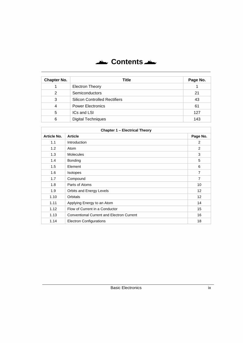
Contents
Basic Electronics ix
Chapter No. Title Page No.
1 Electron Theory 1
2 Semiconductors 21
3 Silicon Controlled Rectifiers 43
4 Power Electronics 61
5 ICs and LSI 127
6 Digital Techniques 143
Chapter 1 – Electrical Theory
Article No. Article Page No.
1.1 Introduction 2
1.2 Atom 2
1.3 Molecules 3
1.4 Bonding 5
1.5 Element 6
1.6 Isotopes 7
1.7 Compound 7
1.8 Parts of Atoms 10
1.9 Orbits and Energy Levels 12
1.10 Orbitals 12
1.11 Applying Energy to an Atom 14
1.12 Flow of Current in a Conductor 15
1.13 Conventional Current and Electron Current 16
1.14 Electron Configurations 18
Contents
Basic Electronics x
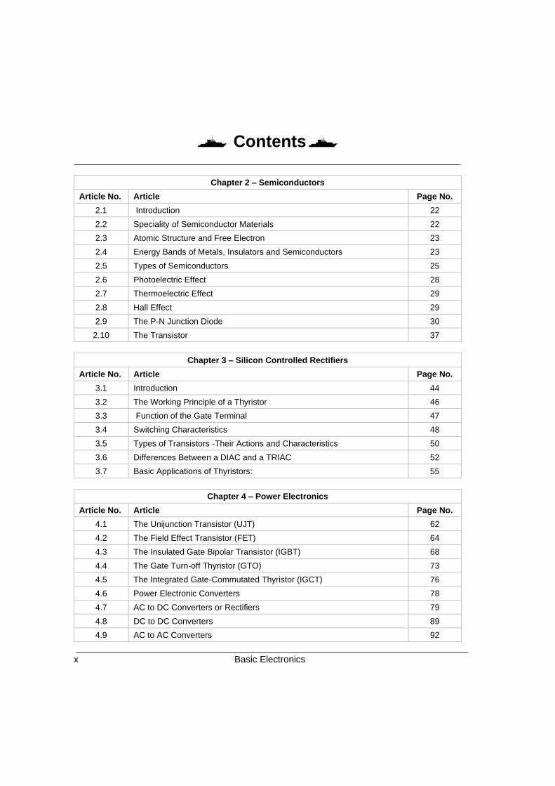
Chapter 2 – Semiconductors
Article No. Article Page No.
2.1 Introduction 22
2.2 Speciality of Semiconductor Materials 22
2.3 Atomic Structure and Free Electron 23
2.4 Energy Bands of Metals, Insulators and Semiconductors 23
2.5 Types of Semiconductors 25
2.6 Photoelectric Effect 28
2.7 Thermoelectric Effect 29
2.8 Hall Effect 29
2.9 The P-N Junction Diode 30
2.10 The Transistor 37
Chapter 3 – Silicon Controlled Rectifiers
Article No. Article Page No.
3.1 Introduction 44
3.2 The Working Principle of a Thyristor 46
3.3 Function of the Gate Terminal 47
3.4 Switching Characteristics 48
3.5 Types of Transistors -Their Actions and Characteristics 50
3.6 Differences Between a DIAC and a TRIAC 52
3.7 Basic Applications of Thyristors: 55
Chapter 4 – Power Electronics
Article No. Article Page No.
4.1 The Unijunction Transistor (UJT) 62
4.2 The Field Effect Transistor (FET) 64
4.3 The Insulated Gate Bipolar Transistor (IGBT) 68
4.4 The Gate Turn-off Thyristor (GTO) 73
4.5 The Integrated Gate-Commutated Thyristor (IGCT) 76
4.6 Power Electronic Converters 78
4.7 AC to DC Converters or Rectifiers 79
4.8 DC to DC Converters 89
4.9 AC to AC Converters 92
Contents
Basic Electronics xi
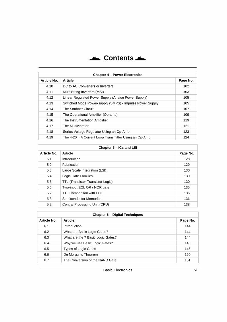
Chapter 4 – Power Electronics
Article No. Article Page No.
4.10 DC to AC Converters or Inverters 102
4.11 Multi String Inverters (MSI) 103
4.12 Linear Regulated Power Supply (Analog Power Supply) 105
4.13 Switched Mode Power-supply (SMPS) - Impulse Power Supply 105
4.14 The Snubber Circuit 107
4.15 The Operational Amplifier (Op-amp) 109
4.16 The Instrumentation Amplifier 119
4.17 The Multivibrator 121
4.18 Series Voltage Regulator Using an Op-Amp 123
4.19 The 4-20 mA Current Loop Transmitter Using an Op-Amp 124
Chapter 5 – ICs and LSI
Article No. Article Page No.
5.1 Introduction 128
5.2 Fabrication 129
5.3 Large Scale Integration (LSI) 130
5.4 Logic Gate Families 130
5.5 TTL (Transistor-Transistor Logic) 130
5.6 Two-input ECL OR / NOR gate 135
5.7 TTL Comparison with ECL 136
5.8 Semiconductor Memories 136
5.9 Central Processing Unit (CPU) 138
Chapter 6 – Digital Techniques
Article No. Article Page No.
6.1 Introduction 144
6.2 What are Basic Logic Gates? 144
6.3 What are the 7 Basic Logic Gates? 144
6.4 Why we use Basic Logic Gates? 145
6.5 Types of Logic Gates 146
6.6 De Morgan’s Theorem 150
6.7 The Conversion of the NAND Gate 151
Contents
Basic Electronics xii
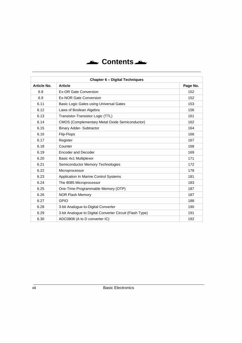
Chapter 6 – Digital Techniques
Article No. Article Page No.
6.8 Ex-OR Gate Conversion 152
6.9 Ex-NOR Gate Conversion 152
6.11 Basic Logic Gates using Universal Gates 153
6.12 Laws of Boolean Algebra 156
6.13 Transistor-Transistor Logic (TTL) 161
6.14 CMOS (Complementary Metal Oxide Semiconductor) 162
6.15 Binary Adder- Subtractor 164
6.16 Flip-Flops 166
6.17 Register 167
6.18 Counter 168
6.19 Encoder and Decoder 169
6.20 Basic 4x1 Multiplexer 171
6.21 Semiconductor Memory Technologies 172
6.22 Microprocessor 178
6.23 Application In Marine Control Systems 181
6.24 The 8085 Microprocessor 183
6.25 One-Time-Programmable Memory (OTP) 187
6.26 NOR Flash Memory 187
6.27 GPIO 188
6.28 3-bit Analogue-to-Digital Converter 190
6.29 3-bit Analogue to Digital Converter Circuit (Flash Type) 191
6.30 ADC0808 (A to D converter IC) 192

Chapter 1 Electron Theory
Basic Electronics for Seafarers
Sir! Why are we studying this
chapter i.e., Electron Theory?
We studied it long ago. Where
will we applicaty this knowledge?
Hello Divyam! Electronics
is the study and use of
devices that control the
flow of electrons. These
devices can be used to
process information or
perform tasks. So, I would
like to start this book by
this chapter because I
want to clear everyone’s
basics first!
Chapter 1
Basic Electronics for Seafarers 2
1.1 Introduction
Atoms are the building blocks of everything you see around: the screen you are looking at,
your study table, your books, etc. Such is the amazing power of nature and also the fundamental
nature of these particles. Despite the discovery of sub-particles like electrons, protons and
neutrons, an atom continues to remain the fundamental particle because of the fact that it is the
smallest unit humans can calculate and model and that which exhibits the chemical properties
of an element.
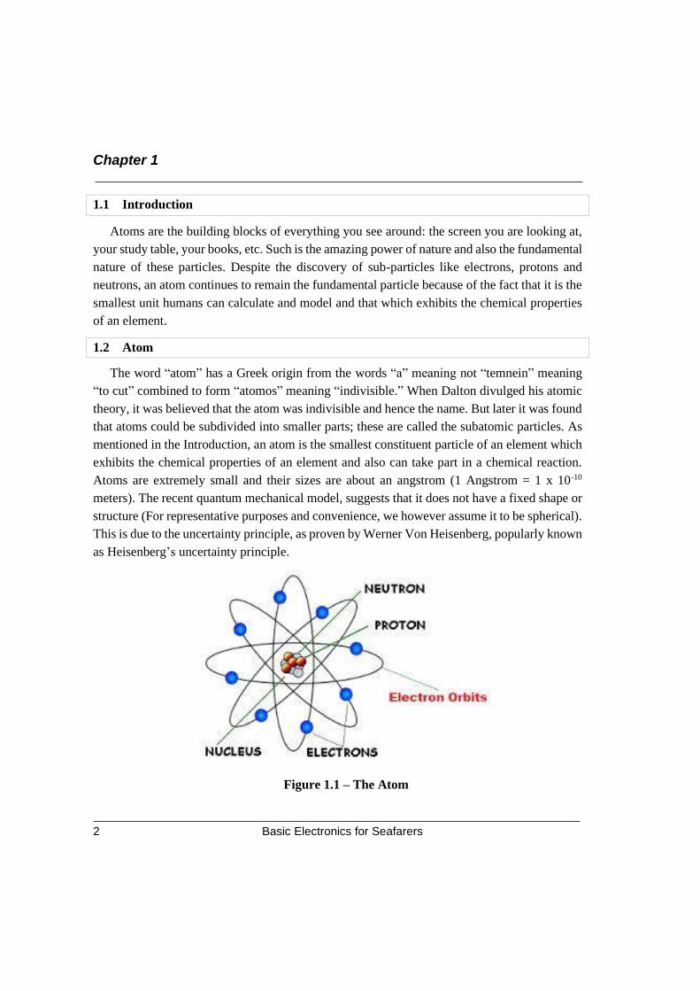
1.2 Atom
The word “atom” has a Greek origin from the words “a” meaning not “temnein” meaning
“to cut” combined to form “atomos” meaning “indivisible.” When Dalton divulged his atomic
theory, it was believed that the atom was indivisible and hence the name. But later it was found
that atoms could be subdivided into smaller parts; these are called the subatomic particles. As
mentioned in the Introduction, an atom is the smallest constituent particle of an element which
exhibits the chemical properties of an element and also can take part in a chemical reaction.
Atoms are extremely small and their sizes are about an angstrom (1 Angstrom = 1 x 10⁻¹⁰
meters). The recent quantum mechanical model, suggests that it does not have a fixed shape or
structure (For representative purposes and convenience, we however assume it to be spherical).
This is due to the uncertainty principle, as proven by Werner Von Heisenberg, popularly known
as Heisenberg’s uncertainty principle.
Figure 1.1 – The Atom
Electron Theory
Basic Electronics for Seafarers 3
Every atom is composed of a nucleus and one or more electrons bound to the nucleus. The
nucleus is made of one or more protons and a number of neutrons. Only the most common
variety of hydrogen has no neutrons.
More than 99.94% of an atom's mass is in the nucleus. The protons have a positive electric
charge, the electrons have a negative electric charge, and the neutrons have no electric charge.
If the number of protons and electrons are equal, then the atom is electrically neutral. If an atom
has more or fewer electrons than protons, then it has an overall negative or positive charge,
respectively – such atoms are called ions.
The electrons of an atom are attracted to the protons in an atomic nucleus by the
electromagnetic force. The protons and neutrons in the nucleus are attracted to each other by
the nuclear force. This force is usually stronger than the electromagnetic force that repels the
positively charged protons from one another. Under certain circumstances, the repelling
electromagnetic force becomes stronger than the nuclear force. In this case, the nucleus splits
and leaves behind different elements. This is a form of nuclear decay. The number of protons
in the nucleus is the atomic number and it defines to which chemical element the atom belongs.
For example, any atom that contains 29 protons, 35 neutrons and 29 electrons is copper (Cu).
The number of neutrons defines the isotope of the element. Atoms can attach to one or more
other atoms by chemical bonds to form chemical compounds such as molecules or crystals. The
ability of atoms to associate and dissociate is responsible for most of the physical changes
observed in nature. Chemistry is the discipline that studies these changes. There were many
theories on the structure of an atom. Some of the most important ones are J.J. Thomson's Model,
Rutherford's Model and Bohr's Model.
1.3 Molecules
Atoms, in general, seem to be extroverts. They can easily combine with one another and
form more complex particles called molecules as mentioned above. Thus, molecules are groups
of atoms held together by chemical bonds and possess no net charge. Molecules can simply be
defined as the way atoms exist in nature. Molecules, in general, are the smallest entities that
can represent the chemical properties of a compound. It is strange to define a molecule using a
compound, and then a compound using the idea of molecules, but they are so interconnected
that it is difficult to find independent definitions. So, molecules are the basic units of everything
that you see around. Molecules are formed when two or more atoms react and chemically
combine under certain conditions. Molecules can be categorized as homo-nuclear and hetero-
nuclear. It is pretty much evident from the names itself.
Chapter 1
Basic Electronics for Seafarers 4
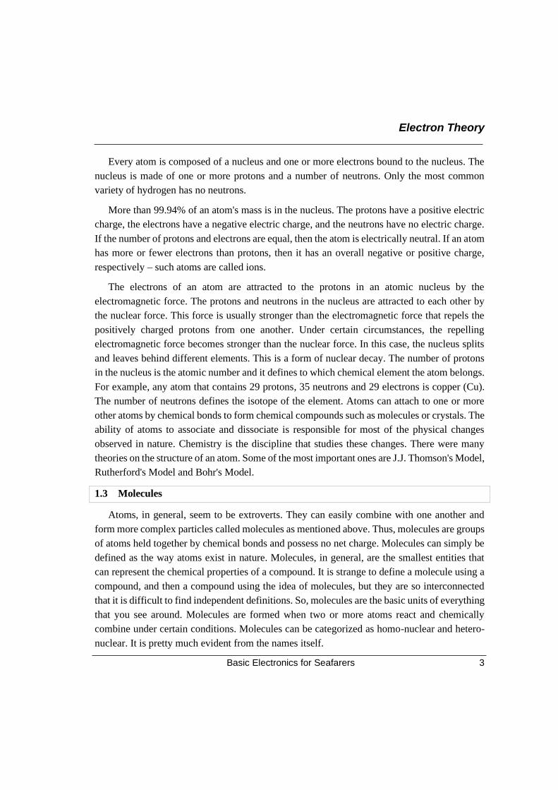
A homo-nuclear molecule is formed when the combining atoms are of the same element.
For example, two hydrogen atoms combine together and form a stable homo-nuclear molecule,
di-hydrogen (H2). It is the smallest molecule with a bond length of 0.74 Å where the Angstrom
(Å), is the unit of length, equal to 10−10 metre, or 0.1 nanometre. A hetero-nuclear molecule
consists of atoms of different elements. For example, when two atoms of hydrogen and an atom
of oxygen chemically combine, they form stable hetero-nuclear compound, water (H2O).
Figure 1.2 – A Water Molecule
Molecules can react with one another to form different molecules and thus different
compounds. It is thus molecules that are in general involved in chemistry and chemical
reactions, much more than atoms. Molecules as components of matter are common. They also
make up most of the oceans and atmosphere. Most organic substances are molecules. The
substances of life are molecules, e.g., proteins, the amino acids they are made of, the nucleic
acids (DNA and RNA), sugars, carbohydrates, fats, and vitamins. The nutrient minerals
ordinarily are not molecules, e.g., iron sulfate. However, the majority of familiar solid
substances on Earth are not made of molecules. These include all of the minerals that make up
the substance of the Earth, soil, dirt, sand, clay, pebbles, rocks, boulders, bedrock, the molten
interior, and the core of the Earth. All of these contain many chemical bonds, but are not made
of identifiable molecules.
Molecules can also be classified on the basis of the interaction between the atoms, i.e., the
nature of the bond between the atoms. It can be covalent, i.e., there is an overlap of electron
cloud of the two interacting atoms and the increased interaction between the overlapping
electrons reduces the energy of the system keeping it intact.
It can also be ionic wherein one of the atoms loses an electron to become a positively
charged ion while the other interacting ion gains an electron to become a negatively charged
ion and these ions are held together by electrostatic forces.
Electron Theory
Basic Electronics for Seafarers 5
1.4 Bonding
Molecules are held together by either covalent bonding or ionic bonding. Several types of
non-metal elements exist only as molecules in the environment. For example, hydrogen only
exists as hydrogen molecule. A molecule of a compound is made out of two or more elements.
A homo-nuclear molecule is made out of two or more atoms of a single element.
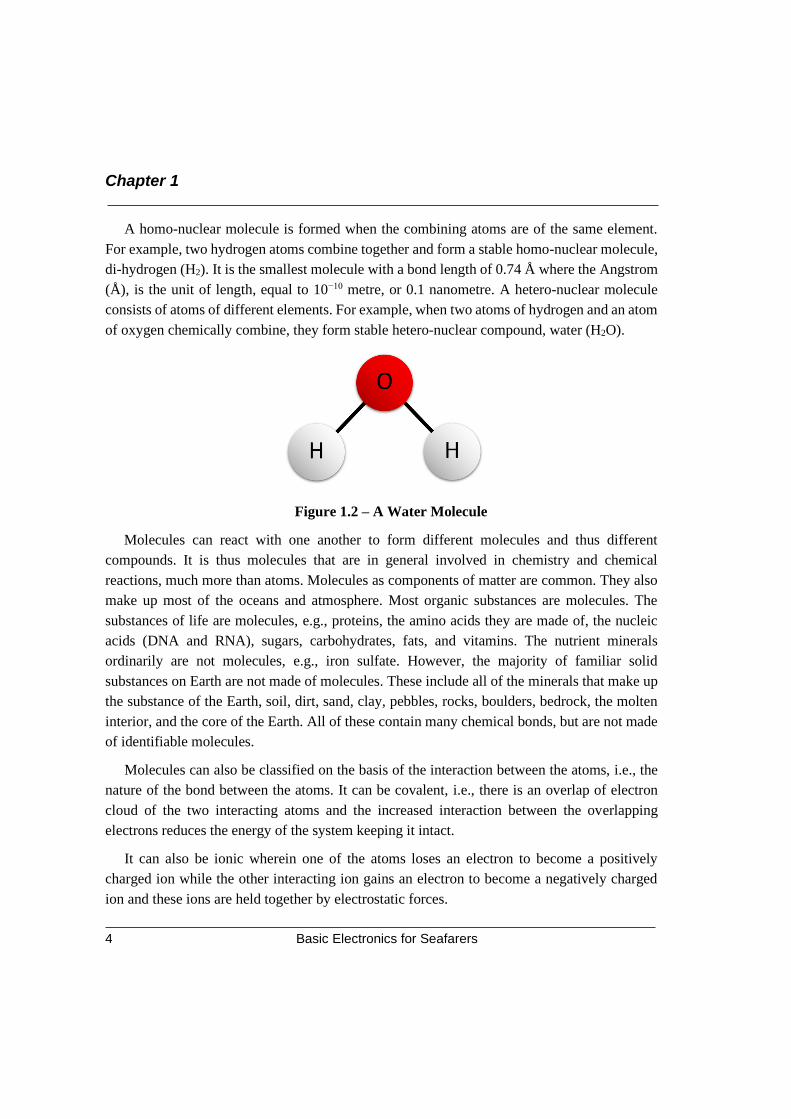
1.4.1 Covalent Bond
A covalent bond forming H2 where two hydrogen atoms share the two electrons. A covalent
bond is a chemical bond that involves the sharing of electron pairs between atoms. These
electron pairs are termed shared pairs or bonding pairs, and the stable balance of attractive and
repulsive forces between atoms, when they share electrons, is termed covalent bonding.
Figure 1.3 – A Covalent Bond
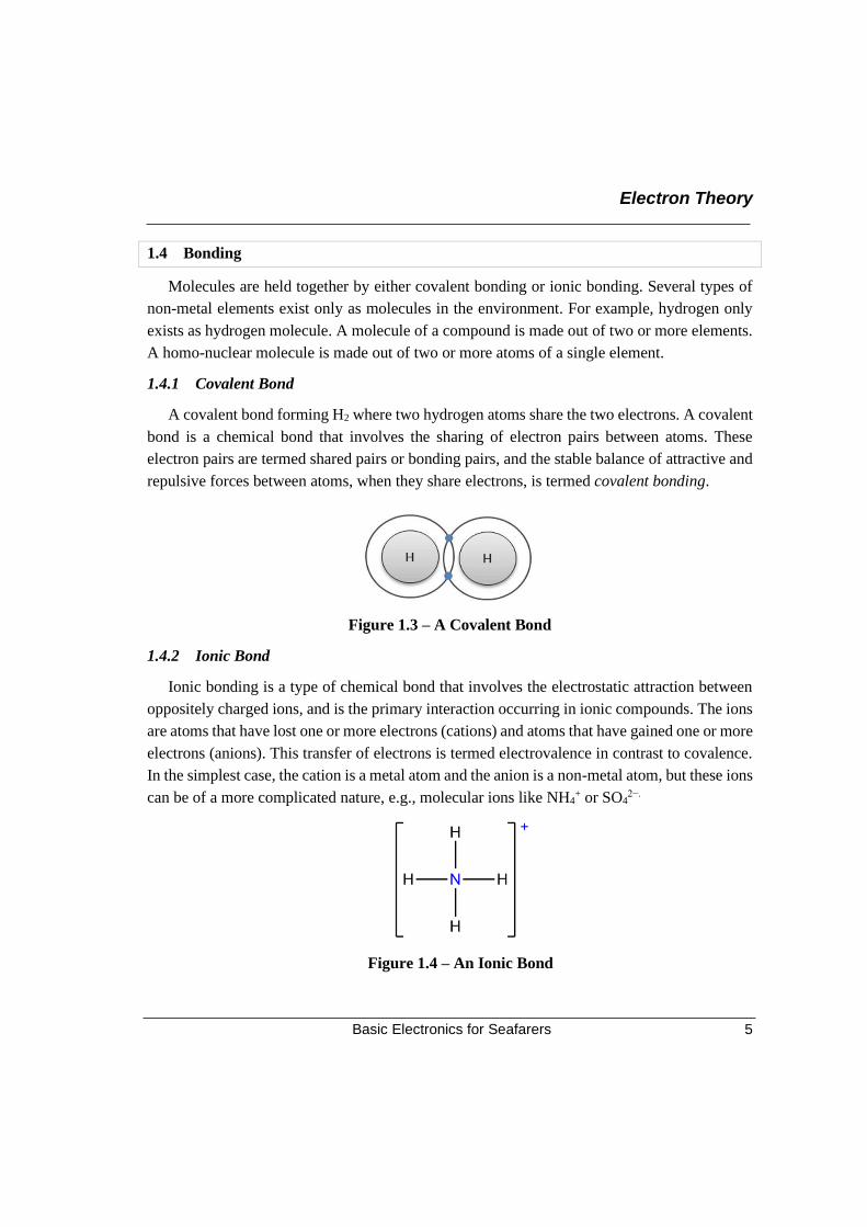
1.4.2 Ionic Bond
Ionic bonding is a type of chemical bond that involves the electrostatic attraction between
oppositely charged ions, and is the primary interaction occurring in ionic compounds. The ions
are atoms that have lost one or more electrons (cations) and atoms that have gained one or more
electrons (anions). This transfer of electrons is termed electrovalence in contrast to covalence.
In the simplest case, the cation is a metal atom and the anion is a non-metal atom, but these ions
can be of a more complicated nature, e.g., molecular ions like NH4+ or SO4
2−.
Figure 1.4 – An Ionic Bond
Chapter 1
Basic Electronics for Seafarers 6
1.5 Element
In chemistry, an element is a pure substance consisting only of atoms that all have the same
number of protons in their atomic nuclei. Unlike chemical compounds, chemical elements
cannot be broken down into simpler substances by chemical means. The number of protons in
the nucleus is the defining property of an element, and is referred to as its atomic number
(represented by the symbol Z) – all atoms with the same atomic number are atoms of the same
element. All of the baryonic matter of the universe is composed of chemical elements. When
different elements undergo chemical reactions, atoms are rearranged into new compounds held
together by chemical bonds. Only a minority of elements, such as silver and gold, are found
uncombined as relatively pure native element minerals. Nearly all other naturally-occurring
elements occur in the Earth as compounds or mixtures. Air is primarily a mixture of the
elements namely nitrogen, oxygen, and argon, though it does contain compounds including
carbon dioxide and water.
The history of the discovery and use of the elements began with primitive human societies
that discovered native minerals like carbon, sulfur, copper and gold. Attempts to classify
materials such as these resulted in the concepts of classical elements, alchemy, and various
similar theories throughout human history.
Much of the modern understanding of elements developed from the work of Dmitri
Mendeleev, a Russian chemist who published the first recognizable Periodic Table in 1869.
This table organizes the elements by increasing atomic number into rows (“periods”) in which
the columns (“groups”) share recurring (“periodic”) physical and chemical properties. The
periodic table summarizes various properties of the elements, allowing chemists to derive
relationships between them and to make predictions about compounds and potential new ones.
By November 2016, the International Union of Pure and Applied Chemistry had recognized a
total of 118 elements in the periodic table. The first 94 occur naturally on earth, and the
remaining 24 are synthetic elements produced in nuclear reactions. Except for unstable
radioactive elements (radionuclides) which decay quickly, nearly all of the elements are
available industrially in varying amounts. The discovery and synthesis of further new elements
is an on-going area of scientific study.
Electron Theory
Basic Electronics for Seafarers 7
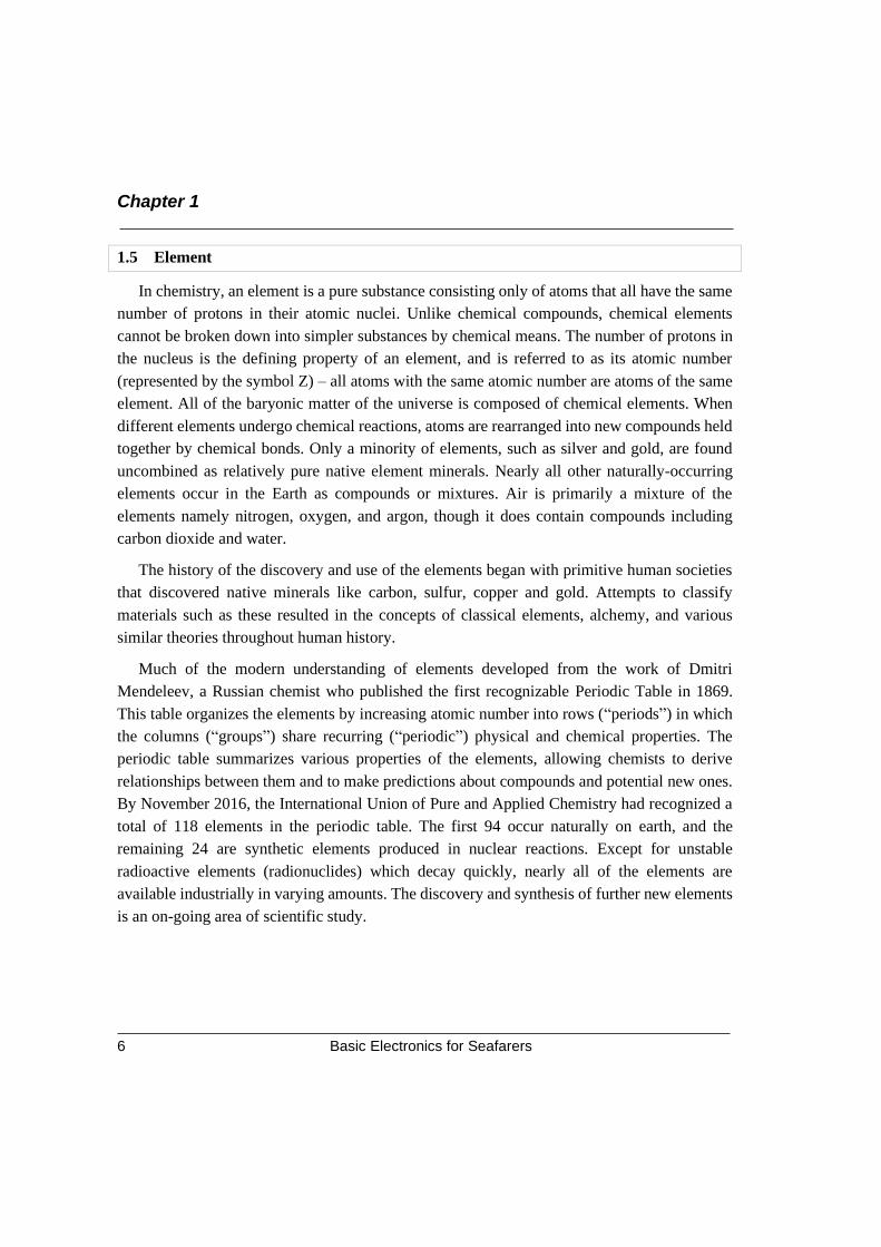
Figure 1.5 – The Periodic Table
1.6 Isotopes
Isotopes are atoms of the same element (that is, with the same number of protons in their
atomic nucleus), but having different numbers of neutrons. Thus, for example, there are three
main isotopes of carbon. All carbon atoms have 6 protons in the nucleus, but they can have
either 6, 7, or 8 neutrons.
Since the mass numbers of these are 12, 13 and 14 respectively, the three isotopes of carbon
are known as carbon-12, carbon-13, and carbon-14, often abbreviated to 12C, 13C, and 14C.
Carbon in everyday life and in chemistry is a mixture of 12C (about 98.9%), 13C (about 1.1%)
and about 1 atom per trillion of 14C. Most (66 of 94) naturally occurring elements have more
than one stable isotope. Except for the isotopes of hydrogen (which differ greatly from each
other in relative mass—enough to cause chemical effects), the isotopes of a given element are
chemically nearly indistinguishable.
1.7 Compound
A chemical compound is a chemical substance composed of many identical molecules (or
molecular entities) composed of atoms from more than one element held together by chemical
bonds. A molecule consisting of atoms of only one element is therefore not a compound.
Chapter 1
Basic Electronics for Seafarers 8
A compound can be converted to a different chemical substance by interaction with a second
substance via a chemical reaction. In this process, bonds between atoms may be broken in either
or both of the interacting substances, and new bonds formed. Any substance consisting of two
or more different types of atoms (chemical elements) in a fixed stoichiometric proportion can
be termed a chemical compound; the concept is most readily understood when considering pure
chemical substances. It follows from their being composed of fixed proportions of two or more
types of atoms that chemical compounds can be converted, via chemical reaction, into
compounds or substances each having fewer atoms. The ratio of each element in the compound
is expressed in a ratio in its chemical formula. A chemical formula is a way of expressing
information about the proportions of atoms that constitute a particular chemical compound,
using the standard abbreviations for the chemical elements, and subscripts to indicate the
number of atoms involved. For example, water is composed of two hydrogen atoms bonded to
one oxygen atom: the chemical formula is H2O and so is CH4. Many chemical compounds have
a unique CAS number identifier assigned by the Chemical Abstracts Service. Globally, more
than 350,000 chemical compounds (including mixtures of chemicals) have been registered for
production and use.
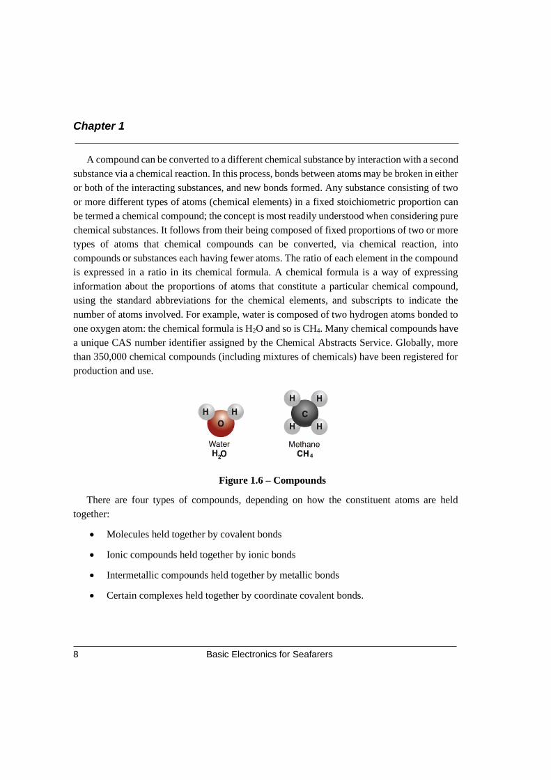
Figure 1.6 – Compounds
There are four types of compounds, depending on how the constituent atoms are held
together:
• Molecules held together by covalent bonds
• Ionic compounds held together by ionic bonds
• Intermetallic compounds held together by metallic bonds
• Certain complexes held together by coordinate covalent bonds.
Electron Theory
Basic Electronics for Seafarers 9
1.7.1 Molecule
A molecule is an electrically neutral group of two or more atoms held together by covalent
bonds. A molecule may be homo-nuclear, that is, it consists of atoms of one chemical element,
as with two atoms in the oxygen molecule (O2); or it may be hetero-nuclear, a chemical
compound composed of more than one element, as with water (two hydrogen atoms and one
oxygen atom; H2O).
1.7.2 Ionic Compounds
An ionic compound is a chemical compound composed of ions held together by electrostatic
forces termed ionic bonding. The compound is neutral overall, but consists of positively
charged ions called cations and negatively charged ions called anions. These can be simple ions
such as the sodium (Na+) and chloride (Cl−) in sodium chloride. Individual ions within an ionic
compound usually have multiple nearest neighbours, so are not considered to be part of
molecules, but instead part of a continuous three-dimensional network, usually in a crystalline
structure.
Ionic compounds containing basic ions hydroxide (OH−) or oxide (O2−) are classified as
bases. Ionic compounds without these ions are also known as salts and can be formed by acid–
base reactions. Ionic compounds can also be produced from their constituent ions by
evaporation of their solvent, precipitation, freezing, a solid-state reaction, or the electron
transfer reaction of reactive metals with reactive non-metals, such as halogen gases. Ionic
compounds typically have high melting and boiling points, and are hard and brittle. As solids
they are almost always electrically insulating, but when melted or dissolved they become highly
conductive, because the ions are mobilized.
1.7.3 Intermetallic Compounds
An intermetallic compound is a type of metallic alloy that forms an ordered solid-state
compound between two or more metallic elements. Intermetallics are generally hard and brittle,
with good high-temperature mechanical properties. They can be classified as stoichiometric or
nonstoichiometic intermetallic compounds.
1.7.4 Complexes
A coordination complex consists of a central atom or ion, which is usually metallic and is
called the coordination centre, and a surrounding array of bound molecules or ions, that are in
turn known as ligands or complexing agents.
Chapter 1
Basic Electronics for Seafarers 10
Many metal-containing compounds, especially those of transition metals, are coordination
complexes. A coordination complex whose centre is a metal atom is called a metal complex of
d block element.
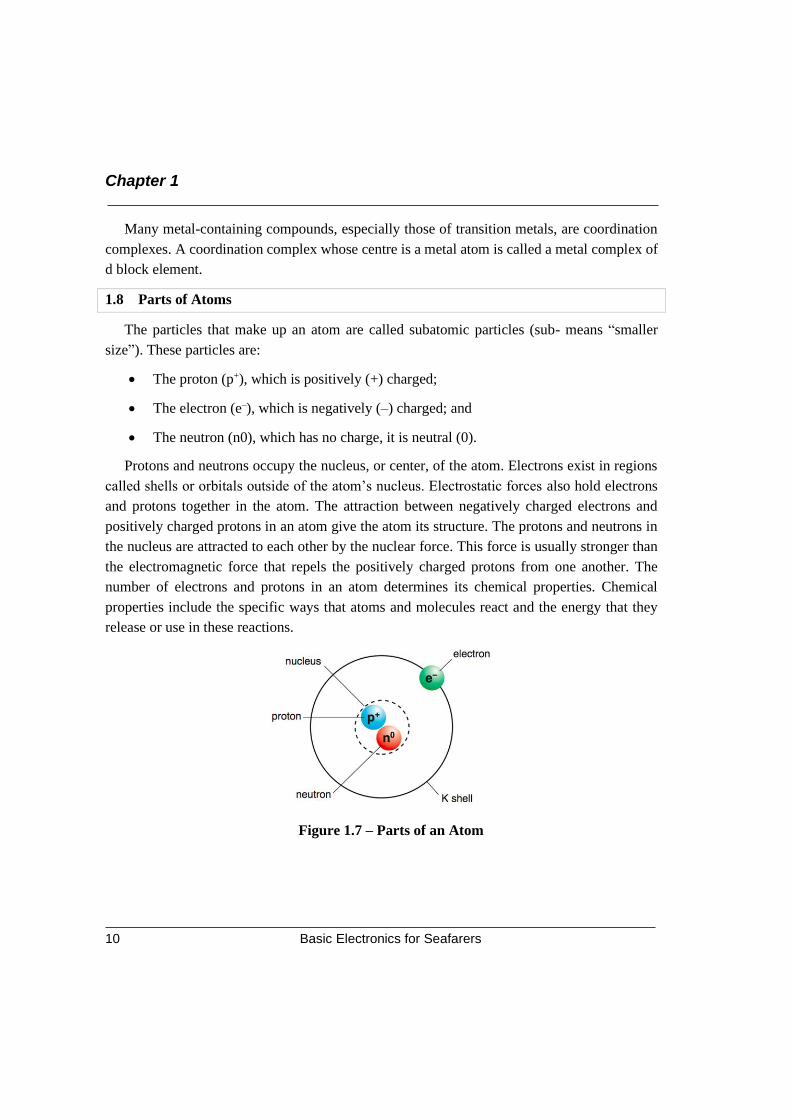
1.8 Parts of Atoms
The particles that make up an atom are called subatomic particles (sub- means “smaller
size”). These particles are:
• The proton (p+), which is positively (+) charged;
• The electron (e–), which is negatively (–) charged; and
• The neutron (n0), which has no charge, it is neutral (0).
Protons and neutrons occupy the nucleus, or center, of the atom. Electrons exist in regions
called shells or orbitals outside of the atom’s nucleus. Electrostatic forces also hold electrons
and protons together in the atom. The attraction between negatively charged electrons and
positively charged protons in an atom give the atom its structure. The protons and neutrons in
the nucleus are attracted to each other by the nuclear force. This force is usually stronger than
the electromagnetic force that repels the positively charged protons from one another. The
number of electrons and protons in an atom determines its chemical properties. Chemical
properties include the specific ways that atoms and molecules react and the energy that they
release or use in these reactions.
Figure 1.7 – Parts of an Atom
Electron Theory
Basic Electronics for Seafarers 11
1.8.1 Size of Subatomic Particles
One hundred million (100,000,000) hydrogen atoms put side-by-side equals about a
centimetre. The protons and neutrons are both about one-thousandth (1/1000) the diameter of a
hydrogen atom. This means it would take about one hundred billion (100,000,000,000) protons
or neutrons put side-by-side to equal a centimetre. Electrons are about one-thousandth (1/1000)
the diameter of a proton or neutron. This means that it would take one hundred trillion
(100,000,000,000,000) electrons put side-by-side to equal a centimetre!
1.8.2 Mass of Subatomic Particles
The electron is by far the least massive of these particles at 9.11×10⁻³¹ kg. Protons have a
mass 1,836 times that of the electron, at 1.6726×10⁻²⁷ kg. Neutrons have a free mass of 1,839
times the mass of the electron, or 1.6749×10⁻²⁷ kg. Neutrons are the heaviest of the three
constituent particles.
1.8.3 Neutral Atoms
The subatomic particles in an atom determine the properties of the atom. Some atoms exist
naturally as neutral, or uncharged, atoms. A single uncharged atom has an equal number of
protons (+) and electrons (–). An uncharged atom is electrically neutral because electrons and
protons have opposite charges of equal sizes. When the number of protons and electrons in an
atom are same, the charges cancel out, or counteract each other.
1.8.4 Atomic Number
Atomic number is nothing but the number of protons present in the nucleus of an atom. It is
denoted by 'Z'. For neutral atoms, it is the number of protons or electrons in an atom.
1.8.5 Atomic Mass Number
An atomic mass number is the sum of numbers of protons and neutrons present in the
nucleus of an atom. It is denoted by 'A'.
Example: An element has 11 protons and 12 neutrons in the nucleus of its atom. Find the
atomic number (Z) and atomic mass number (A) of that element?
Atomic number (Z) = Number of protons = 11
Atomic mass number (A) = Number of protons + Number of neutrons =11 + 12 = 23.
Therefore, the atomic number (Z) and the atomic mass number (A) of that element are 11
and 23.
Chapter 1
Basic Electronics for Seafarers 12
1.9 Orbits and Energy Levels
Unlike planets orbiting the Sun, electrons cannot be at any arbitrary distance from the
nucleus; they can exist only in certain specific locations called allowed orbits. This property,
first explained by Danish physicist Niels Bohr in 1913, In the Bohr atom electrons can be found
only in allowed orbits, and these allowed orbits are at different energies. The orbits are
analogous to a set of stairs in which the gravitational potential energy is different for each step
and in which a ball can be found on any step but never in between. An electron shell, or principal
energy level, may be thought of as the orbit of one or more electrons around an atom's nucleus.
The closest shell to the nucleus is called the “1 shell” (also called “K shell”), followed by the
“2 shell” (or “L shell”), then the “3 shell” (or “M shell”), and so on farther and farther from the
nucleus. The shells correspond with the principal quantum numbers (n = 1, 2, 3, 4 ...) or are
labeled alphabetically with letters used in the X-ray notation (K, L, M, N…). Each shell can
contain only a fixed number of electrons: The first shell can hold up to two electrons, the second
shell can hold up to eight (2 + 6) electrons, the third shell can hold up to 18 (2 + 6 + 10) and so
on. The general formula is that the nth shell can in principle hold up to 2(n2) electrons. Since
electrons are electrically attracted to the nucleus, an atom's electrons will generally occupy
outer shells only if the more inner shells have already been completely filled by other electrons.
However, this is not a strict requirement: atoms may have two or even three incomplete outer
shells. Inside each shell there may be subshells corresponding to different rates of rotation and
orientation of orbitals and the spin directions of the electrons. In general, the farther away from
the nucleus a shell is the more subshells it will have. The subshells are called orbitals.
1.10 Orbitals
It is defined as “the three-dimensional region in space around the nucleus where the
probability of finding the electron is maximum.” An electron can move anywhere in an atom,
even inside the nucleus, or theoretically even at the other side of the universe, but 90%
probability is that it is found in a small specific region of space around the nucleus, and this
region is nothing but the “orbital.” Each orbital in an atom is characterized by a unique set of
values of the three quantum numbers n, ℓ, and ml, which respectively correspond to the
electron's energy (principal quantum number), angular momentum, and an angular momentum
vector component (the magnetic quantum number). Each such orbital can be occupied by a
maximum of two electrons, each with its own projection of spin ms. The simple names s orbital,
p orbital, d orbital, and f orbital refer to orbitals with angular momentum quantum number ℓ =
0, 1, 2, and 3 respectively.
Electron Theory
Basic Electronics for Seafarers 13
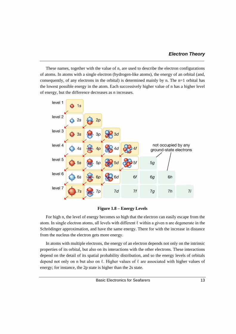
These names, together with the value of n, are used to describe the electron configurations
of atoms. In atoms with a single electron (hydrogen-like atoms), the energy of an orbital (and,
consequently, of any electrons in the orbital) is determined mainly by n. The n=1 orbital has
the lowest possible energy in the atom. Each successively higher value of n has a higher level
of energy, but the difference decreases as n increases.
Figure 1.8 – Energy Levels
For high n, the level of energy becomes so high that the electron can easily escape from the
atom. In single electron atoms, all levels with different ℓ within a given n are degenerate in the
Schrödinger approximation, and have the same energy. There for with the increase in distance
from the nucleus the electron gets more energy.
In atoms with multiple electrons, the energy of an electron depends not only on the intrinsic
properties of its orbital, but also on its interactions with the other electrons. These interactions
depend on the detail of its spatial probability distribution, and so the energy levels of orbitals
depend not only on n but also on ℓ. Higher values of ℓ are associated with higher values of
energy; for instance, the 2p state is higher than the 2s state.

Chapter 1
Basic Electronics for Seafarers 14
When ℓ =2, the increase in energy of the orbital becomes as large as to push the energy of
orbital above the energy of the s-orbital in the next higher shell; when ℓ =3 the energy is pushed
into the shell two steps higher. The filling of the 3d orbitals does not occur until the 4s orbitals
have been filled.
1.11 Applying Energy to an Atom
The laws of quantum mechanics describe the process by which electrons can move from one
allowed orbit, or energy level, to another. As with many processes in the quantum world, this
process is impossible to visualize. An electron disappears from the orbit in which it is located
and reappears in its new location without ever appearing any place in between. This process is
called a quantum leap or quantum jump, and it has no analog in the macroscopic world.
Figure 1.9 – Application of Energy to an Atom
As different orbits have different energies, whenever a quantum leap occurs, the energy
possessed by the electron will be different after the jump. For example, if an electron jumps
from a higher to a lower energy level, the lost energy will have to go somewhere and in fact
will be emitted by the atom in a bundle of electromagnetic radiation. This bundle is known as
a photon, and this emission of photons with a change of energy levels is the process by which
atoms emit light. In the same way, if energy is added to an atom, an electron can use that energy
to make a quantum leap from a lower to a higher orbit.
Electron Theory
Basic Electronics for Seafarers 15
This energy can be supplied in many ways. One common way is for the atom to absorb a
photon of just the right frequency. For example, when white light is shone on an atom, it
selectively absorbs those frequencies corresponding to the energy differences between allowed
orbits.
Each element has a unique set of energy levels, and so the frequencies at which it absorbs
and emits light act as a kind of fingerprint, identifying the particular element. This property of
atoms has given rise to spectroscopy, a science devoted to identifying atoms and molecules by
the kind of radiation they emit or absorb.
1.12 Flow of Current in a Conductor
The way that atoms bond together affects the electrical properties of the materials they form.
For example, in materials held together by the metallic bond, electrons float loosely between
the metal ions. These electrons will be free to move if an electrical force is applied. For example,
if a copper wire is attached across the poles of a battery, the electrons will flow inside the wire.
Thus, electric current flows, and the copper is said to be a conductor.
The flow of electrons inside a conductor is not quite so simple, though. A free electron will
be accelerated for a while but will then collide with an ion. In the collision process, some of the
energy acquired by the electron will be transferred to the ion. As a result, the ion will move
faster, and an observer will notice the wire’s temperature rise. This conversion of electrical
energy from the motion of the electrons to heat energy is called electrical resistance. In a
material of high resistance, the wire heats up quickly as electric current flows. In a material of
low resistance, such as copper wire, most of the energy remains with the moving electrons, so
the material is good at moving electrical energy from one point to another. Its excellent
conducting property, together with its relatively low cost, is why copper is commonly used in
electrical wiring.
The exact opposite situation obtains in materials, such as plastics and ceramics, in which the
electrons are all locked into ionic or covalent bonds. When these kinds of materials are placed
between the poles of a battery, no current flows - there are simply no electrons free to move.
Such materials are called insulators.
While the normal motion of “free” electrons in a conductor is random, with no particular
direction or speed, electrons can be influenced to move in a coordinated fashion through a
conductive material. This uniform motion of electrons is what we call electricity or electric
current.
Chapter 1
Basic Electronics for Seafarers 16
To be more precise, it could be called dynamic electricity in contrast to static electricity,
which is an unmoving accumulation of electric charge. Just like water flowing through the
emptiness of a pipe, electrons are able to move within the empty space within and between the
atoms of a conductor. The conductor may appear to be solid to our eyes, but any material
composed of atoms is mostly empty space! The liquid-flow analogy is so fitting that the motion
of electrons through a conductor is often referred to as a “flow.”
A noteworthy observation may be made here. As each electron moves uniformly through a
conductor, it pushes on the one ahead of it, such that all the electrons move together as a group.
The starting and stopping of electron flow through the length of a conductive path is virtually
instantaneous from one end of a conductor to the other, even though the motion of each electron
may be very slow. An approximate analogy is that of a tube filled end-to-end with marbles: The
tube is full of marbles, just as a conductor is full of free electrons ready to be moved by an
outside influence. If a single marble is suddenly inserted into this full tube on the left-hand side,
another marble will immediately try to exit the tube on the right. Even though each marble only
travelled a short distance, the transfer of motion through the tube is virtually instantaneous from
the left end to the right end, no matter how long the tube is. With electricity, the overall effect
from one end of a conductor to the other happens at the speed of light: a swift 186,000 miles
per second!!! Each individual electron, though, travels through the conductor at a much slower
pace.
1.13 Conventional Current and Electron Current
Electron current and conventional current are two types of notations we use to mention
current flow in a circuit. These two notations are opposite to each other. We need a notation to
do some calculations like in Kirchhoff’s law. And we consider conventional current as the
standard notation of current flow. But actually, this notation is scientifically not correct. But
still, all the laws follow this notation. So, before we get into these notations, we need to
understand charges in electricity.
1.13.1 Charges – Positive and Negative Charges
First of all Franklin assumed an electric charge which moved in the opposite direction that
it should actually be doing, so he called this electric charge “negative” which means deficiency
of charges and so we can consider “positive” means surplus of electric charges. After some
time, true direction of flow of electrons was discovered and it was noticed that this labels of
positive and negative is incorrect scientifically.
Electron Theory
Basic Electronics for Seafarers 17
By that time, the notation of positive and negative was extremely widespread and so no
efforts were made by engineers to change the old notations. As a result of this, we are still using
the same notations that were first assumed by Sir Benjamin Franklin. And this notation we use
now is conventional current notation or normal current flow. Let’s discuss it in detail.
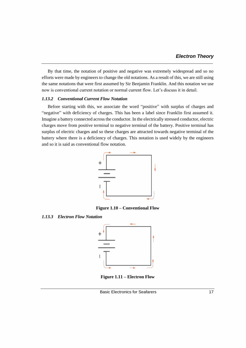
1.13.2 Conventional Current Flow Notation
Before starting with this, we associate the word “positive” with surplus of charges and
“negative” with deficiency of charges. This has been a label since Franklin first assumed it.
Imagine a battery connected across the conductor. In the electrically stressed conductor, electric
charges move from positive terminal to negative terminal of the battery. Positive terminal has
surplus of electric charges and so these charges are attracted towards negative terminal of the
battery where there is a deficiency of charges. This notation is used widely by the engineers
and so it is said as conventional flow notation.
Figure 1.10 – Conventional Flow
1.13.3 Electron Flow Notation
Figure 1.11 – Electron Flow
Chapter 1
Basic Electronics for Seafarers 18
As the name itself says, this notation is based on the movement of electrons. This notation
shows what actually happens inside an electrically stressed conductor. The negative terminal
of battery has high density of electrons. This electron travels from the negative terminal of the
battery where the density of electrons is high to the positive terminal where the density of
electrons is less and that’s why they get attracted towards positive terminal of the battery. Hence
this type of current is known as electron current.
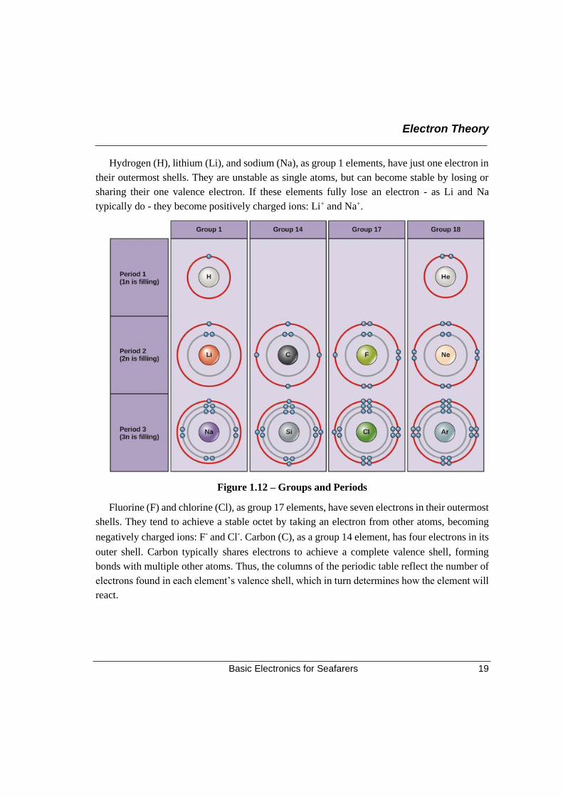
1.14 Electron Configurations
Elements are placed in order on the periodic table based on their atomic number, how many
protons they have. In a neutral atom, the number of electrons will equal the number of protons,
so we can easily determine electron number from atomic number. In addition, the position of
an element in the periodic table - its column, or group, and row, or period—provides useful
information about how those electrons are arranged.
If we consider just the first three rows of the table, which include the major elements
important to life, each row corresponds to the filling of a different electron shell: helium and
hydrogen place their electrons in the 1n shell, while second-row elements like Li start filling
the 2n shell, and third-row elements like Na continue with the 3n shell. Similarly, an element’s
column number gives information about its number of valence electrons. In general, the number
of valence electrons is the same within a column and increases from left to right within a row.
Group 1 elements have just one valence electron and group 18 elements have eight, except for
helium, which has only two electrons total. The number of electrons in the outermost shell of a
particular atom determines its reactivity, or tendency to form chemical bonds with other atoms.
This outermost shell is known as the valence shell, and the electrons found in it are called
valence electrons. In general, atoms are most stable, least reactive, when their outermost
electron shell is full. Most of the elements important in biology need eight electrons in their
outermost shell in order to be stable, and this rule of thumb is known as the octet rule. Some
atoms can be stable with an octet even though their valence shell is the 3n shell, which can hold
up to 18 electrons. Thus, group number is a good predictor of how reactive each element will
be:
Helium (He), neon (Ne), and argon (Ar), as group 18 elements, have outer electron shells
that are full or satisfy the octet rule. This makes them highly stable as single atoms. Because of
their non-reactivity, they are called the inert gases or noble gases.
Electron Theory
Basic Electronics for Seafarers 19
Hydrogen (H), lithium (Li), and sodium (Na), as group 1 elements, have just one electron in
their outermost shells. They are unstable as single atoms, but can become stable by losing or
sharing their one valence electron. If these elements fully lose an electron - as Li and Na
typically do - they become positively charged ions: Li+ and Na+.
Figure 1.12 – Groups and Periods
Fluorine (F) and chlorine (Cl), as group 17 elements, have seven electrons in their outermost
shells. They tend to achieve a stable octet by taking an electron from other atoms, becoming
negatively charged ions: F- and Cl-. Carbon (C), as a group 14 element, has four electrons in its
outer shell. Carbon typically shares electrons to achieve a complete valence shell, forming
bonds with multiple other atoms. Thus, the columns of the periodic table reflect the number of
electrons found in each element’s valence shell, which in turn determines how the element will
react.
Chapter 1
Basic Electronics for Seafarers 20
Sources:
• https://brilliant.org/
• https://en.wikipedia.org/
• https://manoa.hawaii.edu/
• https://www.britannica.com/
• https://www.codrey.com/
Thank You for reading the
first chapter of this book! I
hope I was able to explain to
you, Electron Theory with
respect to Electronics. The
other chapters are going to
be exciting too! So please
follow me to learn the basics
of electronics.

Chapter 2 Semiconductors
Basic Electronics for Seafarers
Sir! What is the
importance of learning
Semi-conductors in
our curriculum?
Semiconductors have a wide
application in electronics. It deals
with the majority of upcoming
technologies. Also, with the
introducton of automation in the
shipping industry, a good
understanding of semiconductors
becomes really important for
freshers like you!
Chapter 2
Basic Electronics for Seafarers 22
2.1 Introduction
All of us are familiar with some of the simple applications of electronics like the radio,
television and the calculator. If you look inside any electronic equipment, you will find
resistors, capacitors, inductors, transformers, semiconductor diodes, transistors and ICs.
We already know something about resistors, capacitors, inductors, and transformers, but
small semiconductor devices like diodes and other related components are new to most of us.
In modem electronic systems, the whole electronic circuit, containing many diodes, transistors,
resistors, etc., are even fabricated on a single chip. This is known as an integrated circuit (IC).
2.2 Speciality of Semiconductor Materials
On the basis of electrical conductivity all the material are classified into three categories,
such as conductor, insulator and semiconductor. We are familiar with a conductor and an
insulator. To reiterate, conductor have good electrical conductivity, the flow of electron with
in conducting material is very smooth if potential difference is applied.
Examples of good conductors are silver, copper etc. The flow of electron is restricted by the
property of resistivity in insulating material. Its electrical conductivity is very less in nature.
Examples of good insulators are rubber, PVC, glass etc.
Apart from these, there is another group of materials whose electrical conductivity is neither
too good as conductor nor too bad as insulator. Its conductivity is in between a conductor and
an insulator, and hence termed as a semiconductor. At room temperature these materials have
conductivities that are considerably lower than that of conductors, but much higher than
insulators. If one increases the temperature, a semiconductor behaves opposite to that of a
metal, i.e., the resistivity decreases and obviously conductivity rises. There are certain
properties which make semiconductor more popular, namely:
1. The conductivity of semiconductor can be controlled.
2. They have a negative temperature coefficient.
3. They have a unidirectional current flow.
4. Less power is required to operate a semiconductor device.
Semiconductors
Basic Electronics for Seafarers 23
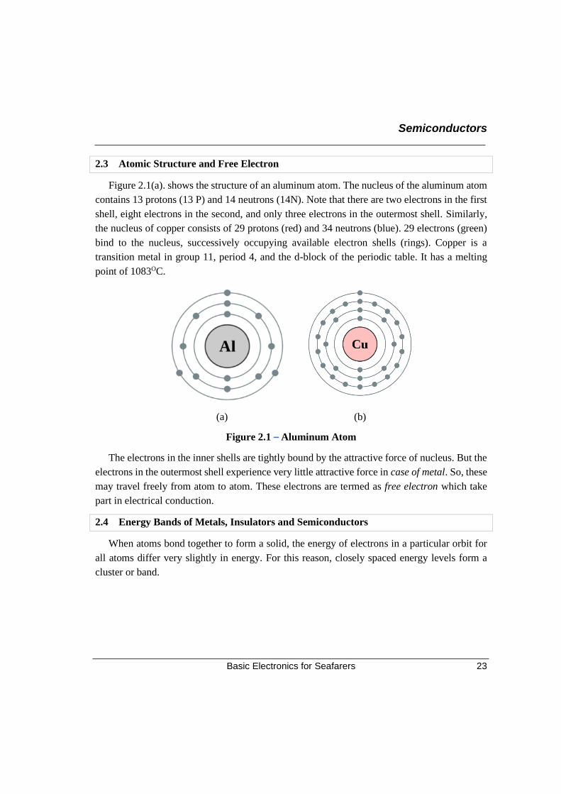
2.3 Atomic Structure and Free Electron
Figure 2.1(a). shows the structure of an aluminum atom. The nucleus of the aluminum atom
contains 13 protons (13 P) and 14 neutrons (14N). Note that there are two electrons in the first
shell, eight electrons in the second, and only three electrons in the outermost shell. Similarly,
the nucleus of copper consists of 29 protons (red) and 34 neutrons (blue). 29 electrons (green)
bind to the nucleus, successively occupying available electron shells (rings). Copper is a
transition metal in group 11, period 4, and the d-block of the periodic table. It has a melting
point of 1083OC.
(a) (b)
Figure 2.1 – Aluminum Atom
The electrons in the inner shells are tightly bound by the attractive force of nucleus. But the
electrons in the outermost shell experience very little attractive force in case of metal. So, these
may travel freely from atom to atom. These electrons are termed as free electron which take
part in electrical conduction.
2.4 Energy Bands of Metals, Insulators and Semiconductors
When atoms bond together to form a solid, the energy of electrons in a particular orbit for
all atoms differ very slightly in energy. For this reason, closely spaced energy levels form a
cluster or band.
Chapter 2
Basic Electronics for Seafarers 24
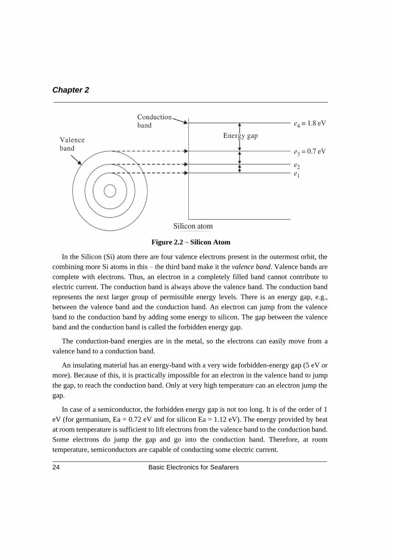
Figure 2.2 – Silicon Atom
In the Silicon (Si) atom there are four valence electrons present in the outermost orbit, the
combining more Si atoms in this – the third band make it the valence band. Valence bands are
complete with electrons. Thus, an electron in a completely filled band cannot contribute to
electric current. The conduction band is always above the valence band. The conduction band
represents the next larger group of permissible energy levels. There is an energy gap, e.g.,
between the valence band and the conduction band. An electron can jump from the valence
band to the conduction band by adding some energy to silicon. The gap between the valence
band and the conduction band is called the forbidden energy gap.
The conduction-band energies are in the metal, so the electrons can easily move from a
valence band to a conduction band.
An insulating material has an energy-band with a very wide forbidden-energy gap (5 eV or
more). Because of this, it is practically impossible for an electron in the valence band to jump
the gap, to reach the conduction band. Only at very high temperature can an electron jump the
gap.
In case of a semiconductor, the forbidden energy gap is not too long. It is of the order of 1
eV (for germanium, Ea = 0.72 eV and for silicon Ea = 1.12 eV). The energy provided by heat
at room temperature is sufficient to lift electrons from the valence band to the conduction band.
Some electrons do jump the gap and go into the conduction band. Therefore, at room
temperature, semiconductors are capable of conducting some electric current.
Semiconductors
Basic Electronics for Seafarers 25
An electron in the conduction band experiences almost negligible nuclear attraction. it
moves randomly throughout the solid. This is why the electrons in the conduction band are
called free electrons.
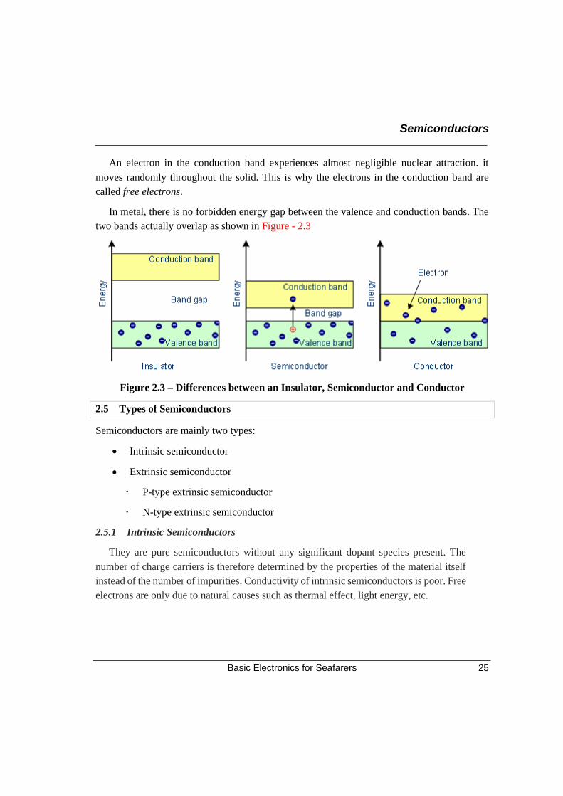
In metal, there is no forbidden energy gap between the valence and conduction bands. The
two bands actually overlap as shown in Figure - 2.3
Figure 2.3 – Differences between an Insulator, Semiconductor and Conductor
2.5 Types of Semiconductors
Semiconductors are mainly two types:
• Intrinsic semiconductor
• Extrinsic semiconductor
P-type extrinsic semiconductor
N-type extrinsic semiconductor
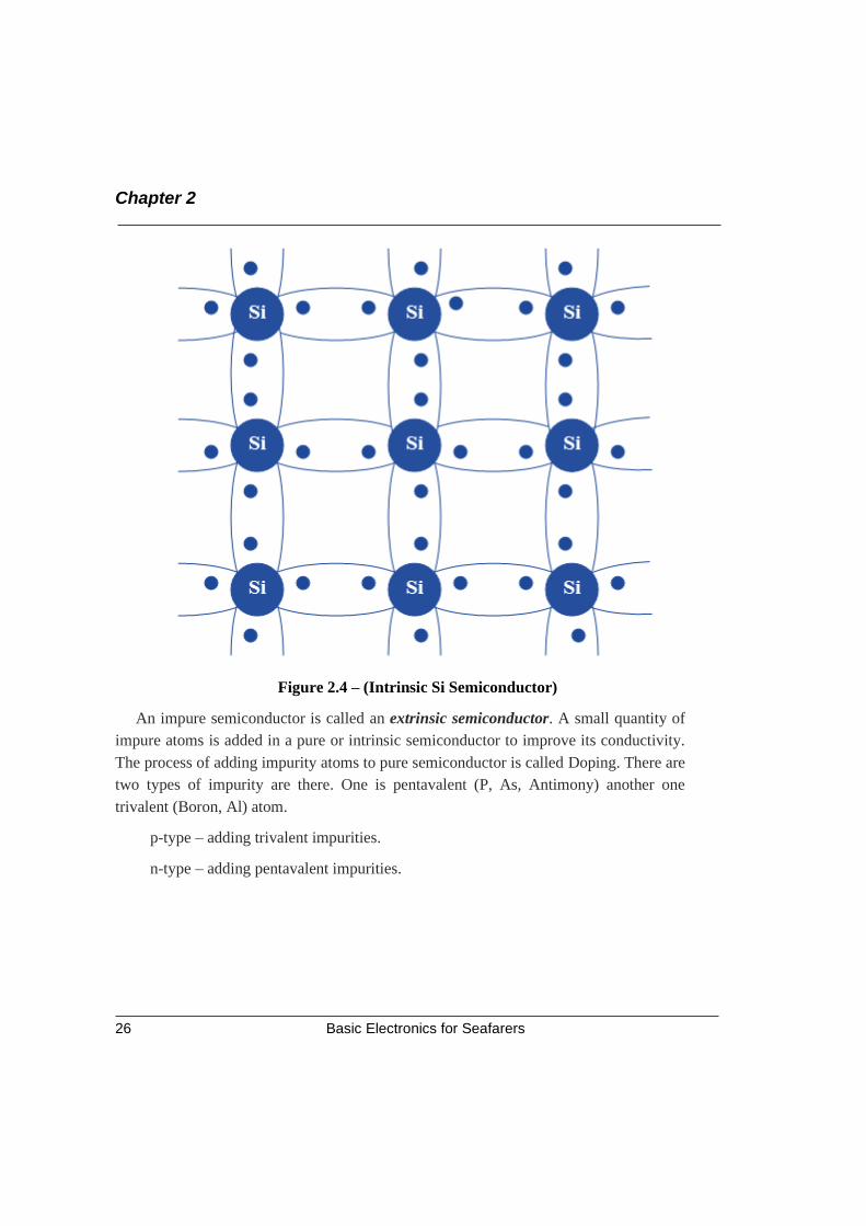
2.5.1 Intrinsic Semiconductors
They are pure semiconductors without any significant dopant species present. The
number of charge carriers is therefore determined by the properties of the material itself
instead of the number of impurities. Conductivity of intrinsic semiconductors is poor. Free
electrons are only due to natural causes such as thermal effect, light energy, etc.
Chapter 2
Basic Electronics for Seafarers 26
Figure 2.4 – (Intrinsic Si Semiconductor)
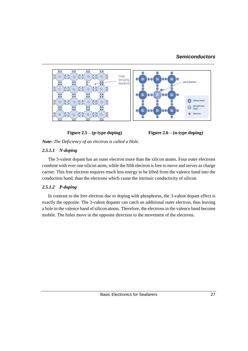
An impure semiconductor is called an extrinsic semiconductor. A small quantity of
impure atoms is added in a pure or intrinsic semiconductor to improve its conductivity.
The process of adding impurity atoms to pure semiconductor is called Doping. There are
two types of impurity are there. One is pentavalent (P, As, Antimony) another one
trivalent (Boron, Al) atom.
p-type – adding trivalent impurities.
n-type – adding pentavalent impurities.
Semiconductors
Basic Electronics for Seafarers 27
Figure 2.5 – (p-type doping) Figure 2.6 – (n-type doping)
Note: The Deficiency of an electron is called a Hole.
2.5.1.1 N-doping
The 5-valent dopant has an outer electron more than the silicon atoms. Four outer electrons
combine with ever one silicon atom, while the fifth electron is free to move and serves as charge
carrier. This free electron requires much less energy to be lifted from the valence band into the
conduction band, than the electrons which cause the intrinsic conductivity of silicon.
2.5.1.2 P-doping
In contrast to the free electron due to doping with phosphorus, the 3-valent dopant effect is
exactly the opposite. The 3-valent dopants can catch an additional outer electron, thus leaving
a hole in the valence band of silicon atoms. Therefore, the electrons in the valence band become
mobile. The holes move in the opposite direction to the movement of the electrons.
Chapter 2
Basic Electronics for Seafarers 28
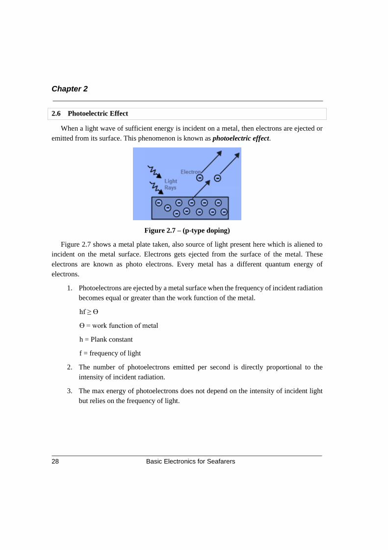
2.6 Photoelectric Effect
When a light wave of sufficient energy is incident on a metal, then electrons are ejected or
emitted from its surface. This phenomenon is known as photoelectric effect.
Figure 2.7 – (p-type doping)
Figure 2.7 shows a metal plate taken, also source of light present here which is aliened to
incident on the metal surface. Electrons gets ejected from the surface of the metal. These
electrons are known as photo electrons. Every metal has a different quantum energy of
electrons.
1. Photoelectrons are ejected by a metal surface when the frequency of incident radiation
becomes equal or greater than the work function of the metal.
hf ≥ Ɵ
Ɵ = work function of metal
h = Plank constant
f = frequency of light
2. The number of photoelectrons emitted per second is directly proportional to the
intensity of incident radiation.
3. The max energy of photoelectrons does not depend on the intensity of incident light
but relies on the frequency of light.
Semiconductors
Basic Electronics for Seafarers 29
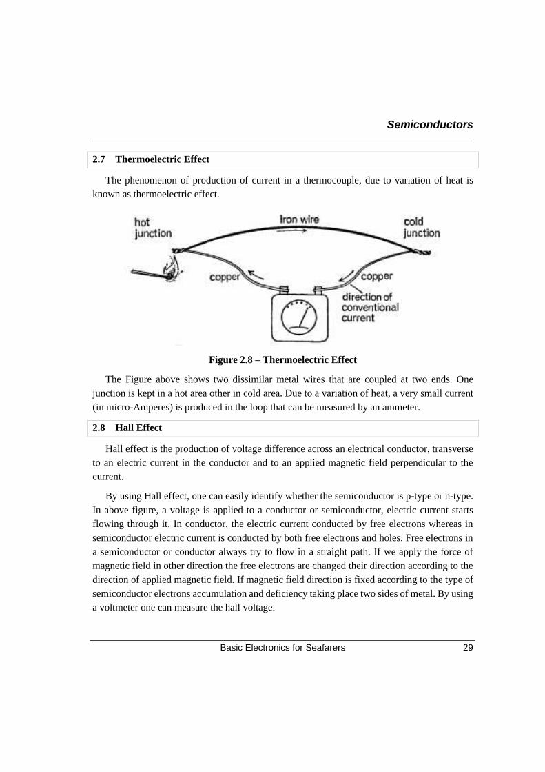
2.7 Thermoelectric Effect
The phenomenon of production of current in a thermocouple, due to variation of heat is
known as thermoelectric effect.
Figure 2.8 – Thermoelectric Effect
The Figure above shows two dissimilar metal wires that are coupled at two ends. One
junction is kept in a hot area other in cold area. Due to a variation of heat, a very small current
(in micro-Amperes) is produced in the loop that can be measured by an ammeter.
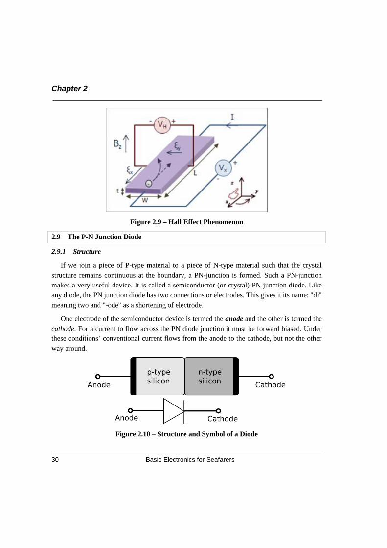
2.8 Hall Effect
Hall effect is the production of voltage difference across an electrical conductor, transverse
to an electric current in the conductor and to an applied magnetic field perpendicular to the
current.
By using Hall effect, one can easily identify whether the semiconductor is p-type or n-type.
In above figure, a voltage is applied to a conductor or semiconductor, electric current starts
flowing through it. In conductor, the electric current conducted by free electrons whereas in
semiconductor electric current is conducted by both free electrons and holes. Free electrons in
a semiconductor or conductor always try to flow in a straight path. If we apply the force of
magnetic field in other direction the free electrons are changed their direction according to the
direction of applied magnetic field. If magnetic field direction is fixed according to the type of
semiconductor electrons accumulation and deficiency taking place two sides of metal. By using
a voltmeter one can measure the hall voltage.
Chapter 2
Basic Electronics for Seafarers 30
Figure 2.9 – Hall Effect Phenomenon
2.9 The P-N Junction Diode
2.9.1 Structure
If we join a piece of P-type material to a piece of N-type material such that the crystal
structure remains continuous at the boundary, a PN-junction is formed. Such a PN-junction
makes a very useful device. It is called a semiconductor (or crystal) PN junction diode. Like
any diode, the PN junction diode has two connections or electrodes. This gives it its name: "di"
meaning two and "-ode" as a shortening of electrode.
One electrode of the semiconductor device is termed the anode and the other is termed the
cathode. For a current to flow across the PN diode junction it must be forward biased. Under
these conditions’ conventional current flows from the anode to the cathode, but not the other
way around.
Figure 2.10 – Structure and Symbol of a Diode
Semiconductors
Basic Electronics for Seafarers 31
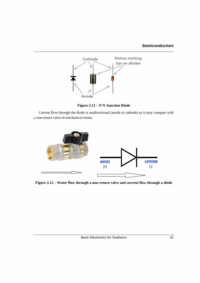
Figure 2.11 – P-N Junction Diode
Current flow through the diode is unidirectional (anode to cathode) so it may compare with
a non-return valve in mechanical terms.
Figure 2.12 – Water flow through a non-return valve and current flow through a diode
Chapter 2
Basic Electronics for Seafarers 32
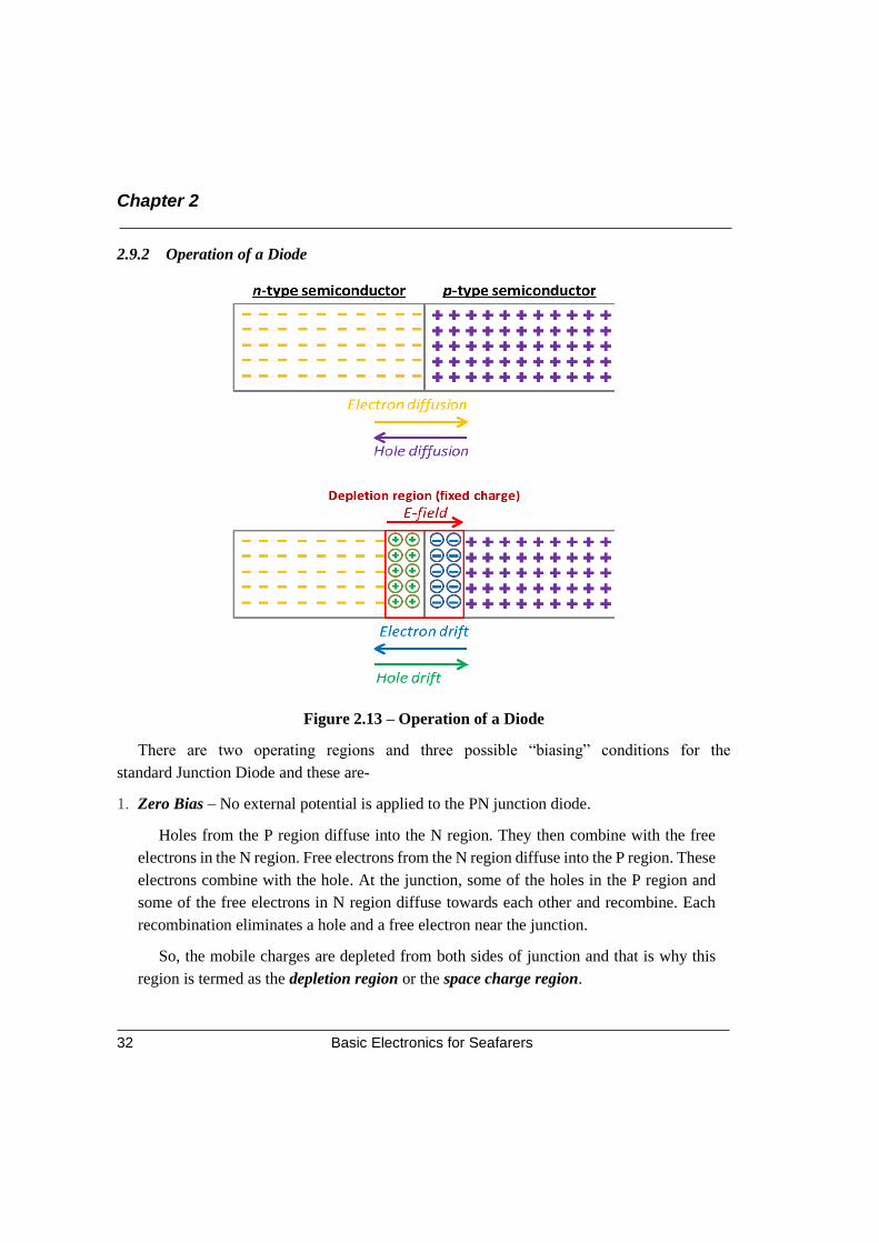
2.9.2 Operation of a Diode
Figure 2.13 – Operation of a Diode
There are two operating regions and three possible “biasing” conditions for the
standard Junction Diode and these are-
1. Zero Bias – No external potential is applied to the PN junction diode.
Holes from the P region diffuse into the N region. They then combine with the free
electrons in the N region. Free electrons from the N region diffuse into the P region. These
electrons combine with the hole. At the junction, some of the holes in the P region and
some of the free electrons in N region diffuse towards each other and recombine. Each
recombination eliminates a hole and a free electron near the junction.
So, the mobile charges are depleted from both sides of junction and that is why this
region is termed as the depletion region or the space charge region.
Semiconductors
Basic Electronics for Seafarers 33
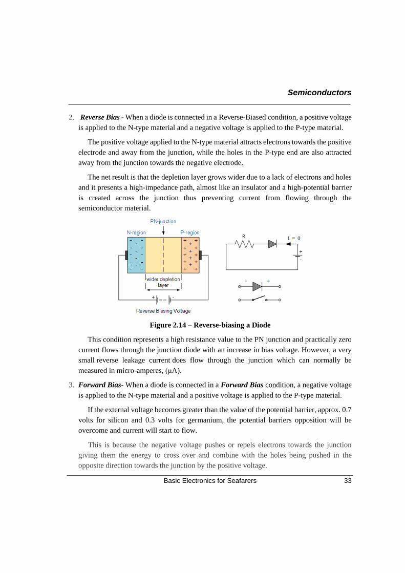
2. Reverse Bias - When a diode is connected in a Reverse-Biased condition, a positive voltage
is applied to the N-type material and a negative voltage is applied to the P-type material.
The positive voltage applied to the N-type material attracts electrons towards the positive
electrode and away from the junction, while the holes in the P-type end are also attracted
away from the junction towards the negative electrode.
The net result is that the depletion layer grows wider due to a lack of electrons and holes
and it presents a high-impedance path, almost like an insulator and a high-potential barrier
is created across the junction thus preventing current from flowing through the
semiconductor material.
Figure 2.14 – Reverse-biasing a Diode
This condition represents a high resistance value to the PN junction and practically zero
current flows through the junction diode with an increase in bias voltage. However, a very
small reverse leakage current does flow through the junction which can normally be
measured in micro-amperes, (μA).
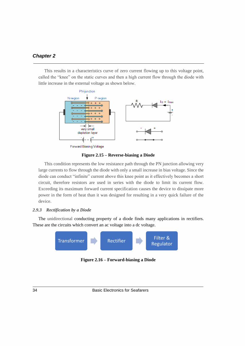
3. Forward Bias- When a diode is connected in a Forward Bias condition, a negative voltage
is applied to the N-type material and a positive voltage is applied to the P-type material.
If the external voltage becomes greater than the value of the potential barrier, approx. 0.7
volts for silicon and 0.3 volts for germanium, the potential barriers opposition will be
overcome and current will start to flow.
This is because the negative voltage pushes or repels electrons towards the junction
giving them the energy to cross over and combine with the holes being pushed in the
opposite direction towards the junction by the positive voltage.
Chapter 2
Basic Electronics for Seafarers 34
This results in a characteristics curve of zero current flowing up to this voltage point,
called the “knee” on the static curves and then a high current flow through the diode with
little increase in the external voltage as shown below.
Figure 2.15 – Reverse-biasing a Diode
This condition represents the low resistance path through the PN junction allowing very
large currents to flow through the diode with only a small increase in bias voltage. Since the
diode can conduct “infinite” current above this knee point as it effectively becomes a short
circuit, therefore resistors are used in series with the diode to limit its current flow.
Exceeding its maximum forward current specification causes the device to dissipate more
power in the form of heat than it was designed for resulting in a very quick failure of the
device.
2.9.3 Rectification by a Diode
The unidirectional conducting property of a diode finds many applications in rectifiers.
These are the circuits which convert an ac voltage into a dc voltage.
Figure 2.16 – Forward-biasing a Diode
Transformer RectifierFilter &
Regulator
Semiconductors
Basic Electronics for Seafarers 35
There are three types of diode rectifiers:
• Half-wave rectifier
• Full-wave rectifier
• Bridge rectifier
We shall discuss only a bridge rectifier as other operations are the same as a bridge rectifier.
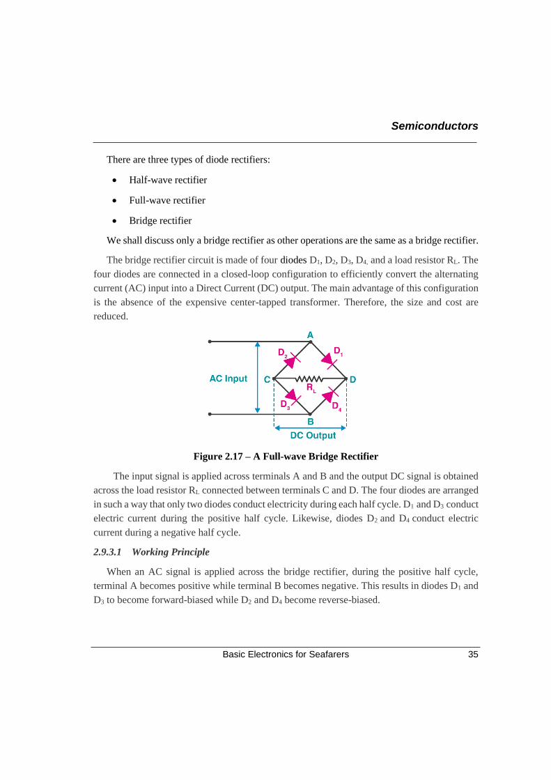
The bridge rectifier circuit is made of four diodes D1, D2, D3, D4, and a load resistor RL. The
four diodes are connected in a closed-loop configuration to efficiently convert the alternating
current (AC) input into a Direct Current (DC) output. The main advantage of this configuration
is the absence of the expensive center-tapped transformer. Therefore, the size and cost are
reduced.
Figure 2.17 – A Full-wave Bridge Rectifier
The input signal is applied across terminals A and B and the output DC signal is obtained
across the load resistor RL connected between terminals C and D. The four diodes are arranged
in such a way that only two diodes conduct electricity during each half cycle. D1 and D3 conduct
electric current during the positive half cycle. Likewise, diodes D2 and D4 conduct electric
current during a negative half cycle.
2.9.3.1 Working Principle
When an AC signal is applied across the bridge rectifier, during the positive half cycle,
terminal A becomes positive while terminal B becomes negative. This results in diodes D1 and
D3 to become forward-biased while D2 and D4 become reverse-biased.
Chapter 2
Basic Electronics for Seafarers 36
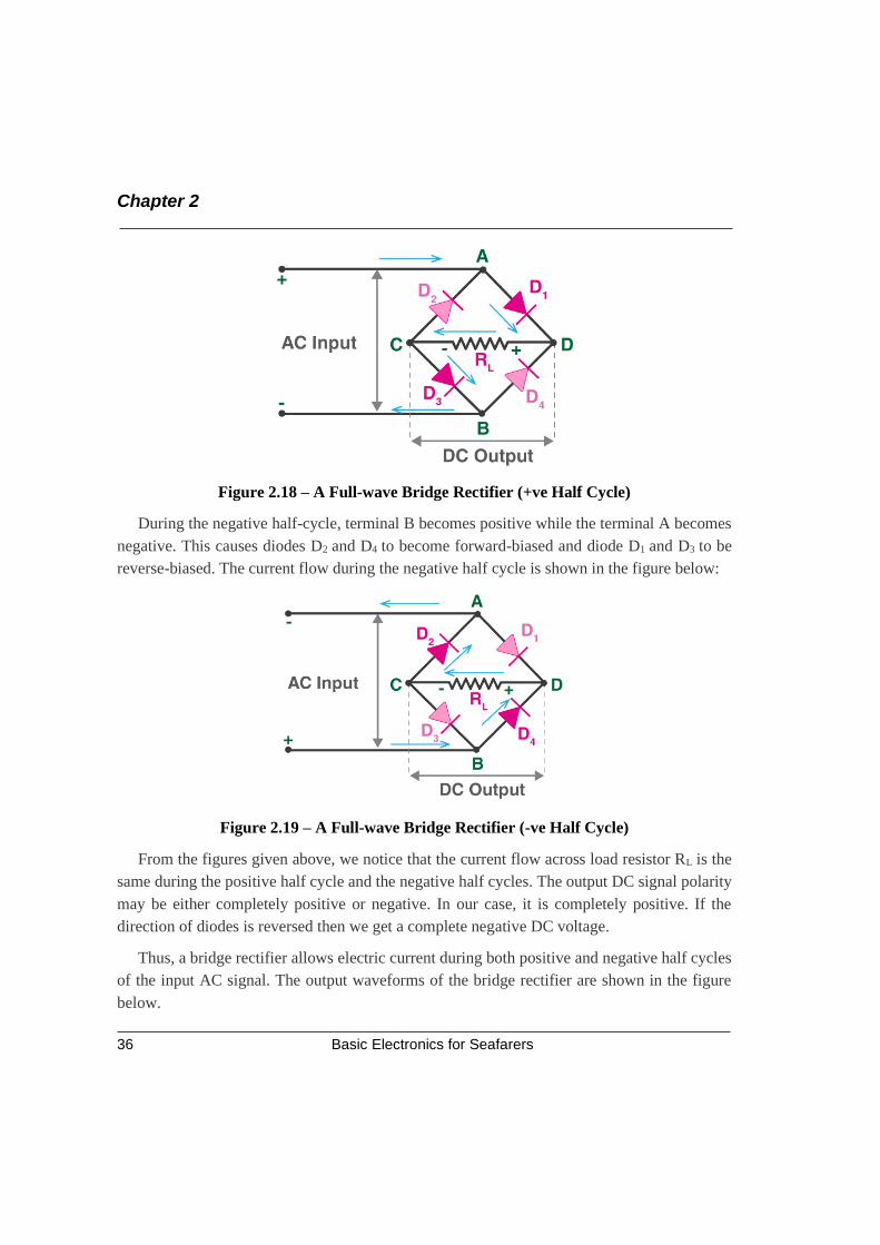
Figure 2.18 – A Full-wave Bridge Rectifier (+ve Half Cycle)
During the negative half-cycle, terminal B becomes positive while the terminal A becomes
negative. This causes diodes D2 and D4 to become forward-biased and diode D1 and D3 to be
reverse-biased. The current flow during the negative half cycle is shown in the figure below:
Figure 2.19 – A Full-wave Bridge Rectifier (-ve Half Cycle)
From the figures given above, we notice that the current flow across load resistor RL is the
same during the positive half cycle and the negative half cycles. The output DC signal polarity
may be either completely positive or negative. In our case, it is completely positive. If the
direction of diodes is reversed then we get a complete negative DC voltage.
Thus, a bridge rectifier allows electric current during both positive and negative half cycles
of the input AC signal. The output waveforms of the bridge rectifier are shown in the figure
below.
Semiconductors
Basic Electronics for Seafarers 37
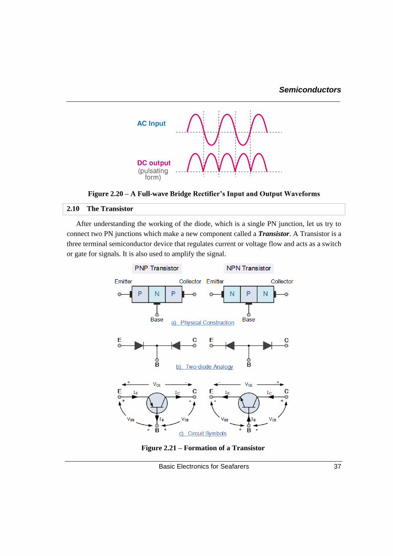
Figure 2.20 – A Full-wave Bridge Rectifier’s Input and Output Waveforms
2.10 The Transistor
After understanding the working of the diode, which is a single PN junction, let us try to
connect two PN junctions which make a new component called a Transistor. A Transistor is a
three terminal semiconductor device that regulates current or voltage flow and acts as a switch
or gate for signals. It is also used to amplify the signal.
Figure 2.21 – Formation of a Transistor
Chapter 2
Basic Electronics for Seafarers 38
The basic construction of a Bipolar Transistor is based on two PN-junctions producing three
connecting terminals, with each terminal being given a name to identify it from the other two.
These three terminals are known and labeled as the Emitter (E), the Base (B) and
the Collector (C) respectively.
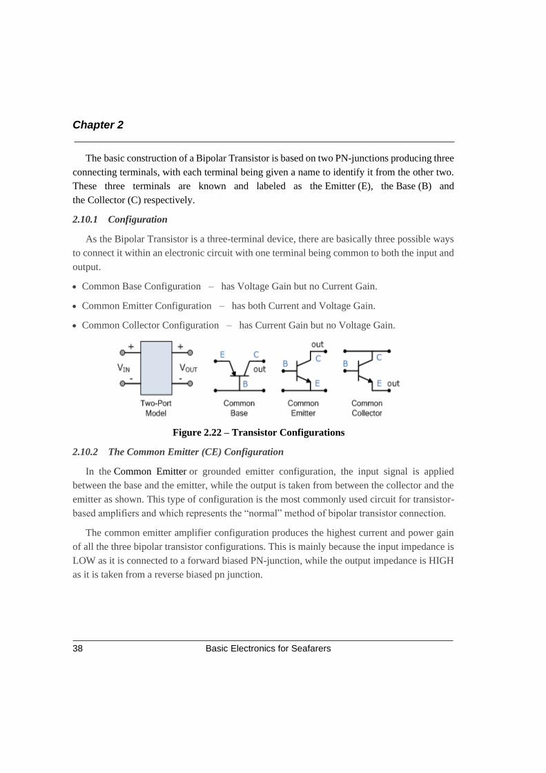
2.10.1 Configuration
As the Bipolar Transistor is a three-terminal device, there are basically three possible ways
to connect it within an electronic circuit with one terminal being common to both the input and
output.
• Common Base Configuration – has Voltage Gain but no Current Gain.
• Common Emitter Configuration – has both Current and Voltage Gain.
• Common Collector Configuration – has Current Gain but no Voltage Gain.
Figure 2.22 – Transistor Configurations
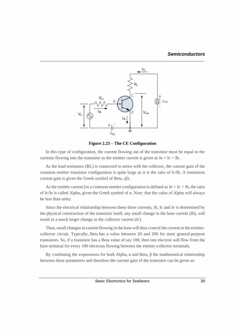
2.10.2 The Common Emitter (CE) Configuration
In the Common Emitter or grounded emitter configuration, the input signal is applied
between the base and the emitter, while the output is taken from between the collector and the
emitter as shown. This type of configuration is the most commonly used circuit for transistor-
based amplifiers and which represents the “normal” method of bipolar transistor connection.
The common emitter amplifier configuration produces the highest current and power gain
of all the three bipolar transistor configurations. This is mainly because the input impedance is
LOW as it is connected to a forward biased PN-junction, while the output impedance is HIGH
as it is taken from a reverse biased pn junction.
Semiconductors
Basic Electronics for Seafarers 39
Figure 2.23 – The CE Configuration
In this type of configuration, the current flowing out of the transistor must be equal to the
currents flowing into the transistor as the emitter current is given as Ie = Ic + Ib.
As the load resistance (RL) is connected in series with the collector, the current gain of the
common emitter transistor configuration is quite large as it is the ratio of Ic/Ib. A transistors
current gain is given the Greek symbol of Beta, (β).
As the emitter current for a common emitter configuration is defined as Ie = Ic + Ib, the ratio
of Ic/Ie is called Alpha, given the Greek symbol of α. Note: that the value of Alpha will always
be less than unity.
Since the electrical relationship between these three currents, Ib, Ic and Ie is determined by
the physical construction of the transistor itself, any small change in the base current (Ib), will
result in a much larger change in the collector current (Ic).
Then, small changes in current flowing in the base will thus control the current in the emitter-
collector circuit. Typically, Beta has a value between 20 and 200 for most general-purpose
transistors. So, if a transistor has a Beta value of say 100, then one electron will flow from the
base terminal for every 100 electrons flowing between the emitter-collector terminals.
By combining the expressions for both Alpha, α and Beta, β the mathematical relationship
between these parameters and therefore the current gain of the transistor can be given as:
Chapter 2
Basic Electronics for Seafarers 40
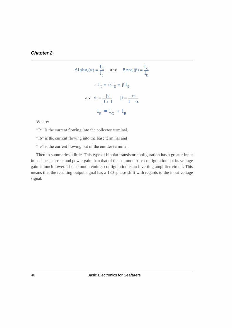
Where:
“Ic” is the current flowing into the collector terminal,
“Ib” is the current flowing into the base terminal and
“Ie” is the current flowing out of the emitter terminal.
Then to summaries a little. This type of bipolar transistor configuration has a greater input
impedance, current and power gain than that of the common base configuration but its voltage
gain is much lower. The common emitter configuration is an inverting amplifier circuit. This
means that the resulting output signal has a 180o phase-shift with regards to the input voltage
signal.
Semiconductors
Basic Electronics for Seafarers 41
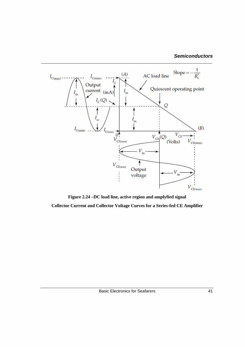
Figure 2.24 –DC load line, active region and amplyfied signal
Collector Current and Collector Voltage Curves for a Series-fed CE Amplifier

Chapter 2
Basic Electronics for Seafarers 42
Sources
• https://www.electronics-tutorials.ws
• https://byjus.com/physics/bridge-rectifier
• Basic Electronics and Linear Circuits by N N Bhargava
• https://www.engineeringprojects.com
• Wikipedia
Hello its Divyam here! I hope that
everyone reading this book
understood the basic concepts of
semiconductors as I did. These basics
are going to help us while working on
Electronic Equipment on board and
likewise ashore too!

Chapter 3 Silicon Controlled Rectifiers
Basic Electronics for Seafarers
Surely Divyam! I hope you are
doing fine. Today I am going to
clear all your doubts about the
Thyristor. It has a wide range
of applications e.g., in variable
speed motor drives and it is
also used in controlling high
power electrical applications.
Sir! Though I’ve already
studied about Thyristors
before. But it is a very
confusing topic. I find it very
difficult to understand its
working and applications.
Please help me Sir!
Chapter 3
Basic Electronics for Seafarers 44
3.1 Introduction
In general, Thyristors are switching devices which are similar to the transistors. Transistors
are the tiny electronic components that changed the world, today we can often find them in
every electronic device like TVs, mobiles, laptops, calculators, earphones etc. They are
adaptable and versatile, but it doesn’t mean that they can be used in every application, we can
use them as amplifying and switching devices but they cannot handle higher current, also a
transistor requires a continuous switching current. So, for all these issues and to overcome these
problems we use thyristors.
Generally, the terms SCR and Thyristor (from Thyratron and Transistor) are used
interchangeably but the SCR is a kind of Thyristor. The mercury-arc valve was the basis of dc
technology back in the day. Engineers in Europe followed the English convention of referring
to tubes (vacuum tubes used in early radios) as valves, so the mercury-arc valve name became
common.
In 1921, some GE engineers modified the mercury-arc valve with a gas filled tube they
called a thyratron. The word thyratron was formed from the Greek words thyra meaning gate
and tron meaning tube.
Then in 1957 another group of GE engineers developed the SCR, which many compared to
a transistor capable of handling high-power. So, it was natural that someone combined the
words thyratron and transistor to form our favored term thyristor. The name became so popular
that in 1963 the IEEE (Institute of Electrical and Electronic Engineers adopted thyristor as the
official name.
A Thyristor includes many types of switches, some of them are SCR (Silicon Controlled
Rectifier), GTO (Gate Turn OFF), and IGBT (Insulated Gate Controlled Bipolar Transistor)
etc. But SCR is the most widely used device, so the word Thyristor became synonymous to
SCR. Simply, SCR is a kind of Thyristor.
Silicon Controlled Rectifiers
Basic Electronics for Seafarers 45
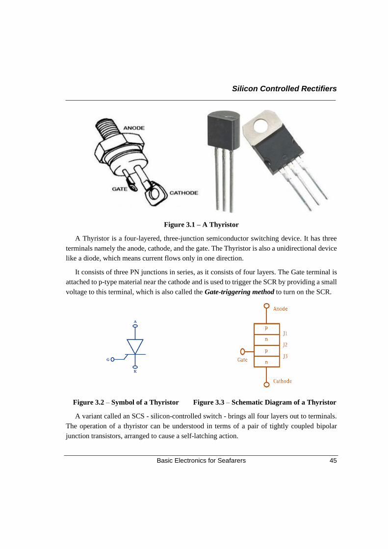
Figure 3.1 – A Thyristor
A Thyristor is a four-layered, three-junction semiconductor switching device. It has three
terminals namely the anode, cathode, and the gate. The Thyristor is also a unidirectional device
like a diode, which means current flows only in one direction.
It consists of three PN junctions in series, as it consists of four layers. The Gate terminal is
attached to p-type material near the cathode and is used to trigger the SCR by providing a small
voltage to this terminal, which is also called the Gate-triggering method to turn on the SCR.
Figure 3.2 – Symbol of a Thyristor Figure 3.3 – Schematic Diagram of a Thyristor
A variant called an SCS - silicon-controlled switch - brings all four layers out to terminals.
The operation of a thyristor can be understood in terms of a pair of tightly coupled bipolar
junction transistors, arranged to cause a self-latching action.
Chapter 3
Basic Electronics for Seafarers 46
Thyristors have three states:
1. Reverse Blocking Mode - Voltage is applied in the direction that would be blocked by a
diode
2. Forward Blocking Mode - Voltage is applied in the direction that would cause a diode to
conduct, but the thyristor has not yet been triggered into conduction
3. Forward Conducting Mode - The thyristor has been triggered into conduction and will
remain conducting until the forward current known as the "holding current", drops below a
threshold value
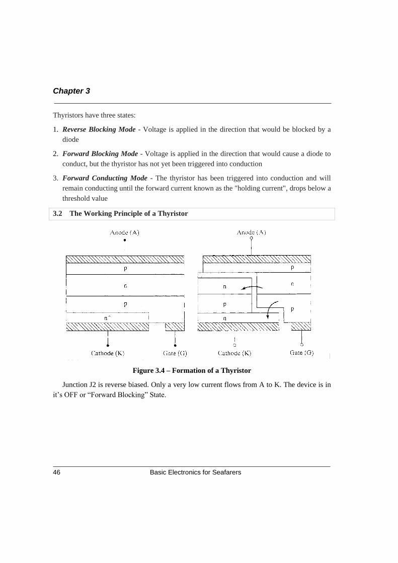
3.2 The Working Principle of a Thyristor
Apply a forward bias voltage to the Anode-Cathode Junctions J1 and J3 are forward biased
Figure 3.4 – Formation of a Thyristor
Junction J2 is reverse biased. Only a very low current flows from A to K. The device is in
it’s OFF or “Forward Blocking” State.
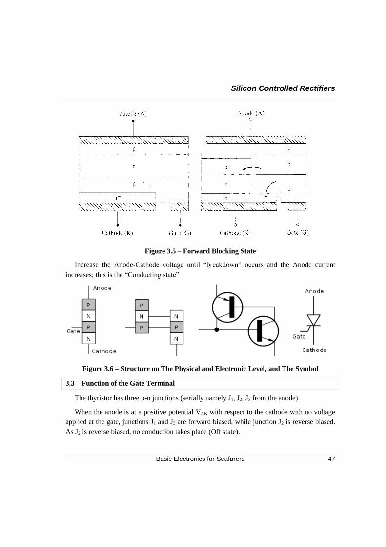
Silicon Controlled Rectifiers
Basic Electronics for Seafarers 47
Figure 3.5 – Forward Blocking State
Increase the Anode-Cathode voltage until “breakdown” occurs and the Anode current
increases; this is the “Conducting state”
Figure 3.6 – Structure on The Physical and Electronic Level, and The Symbol
3.3 Function of the Gate Terminal
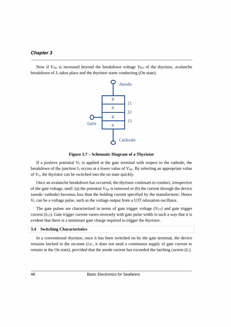
The thyristor has three p-n junctions (serially namely J1, J2, J3 from the anode).
When the anode is at a positive potential VAK with respect to the cathode with no voltage
applied at the gate, junctions J1 and J3 are forward biased, while junction J2 is reverse biased.
As J2 is reverse biased, no conduction takes place (Off state).
Chapter 3
Basic Electronics for Seafarers 48
Now if VAK is increased beyond the breakdown voltage VBO of the thyristor, avalanche
breakdown of J2 takes place and the thyristor starts conducting (On state).
Figure 3.7 – Schematic Diagram of a Thyristor
If a positive potential VG is applied at the gate terminal with respect to the cathode, the
breakdown of the junction J2 occurs at a lower value of VAK. By selecting an appropriate value
of VG, the thyristor can be switched into the on state quickly.
Once an avalanche breakdown has occurred, the thyristor continues to conduct, irrespective
of the gate voltage, until: (a) the potential VAK is removed or (b) the current through the device
(anode−cathode) becomes less than the holding current specified by the manufacturer. Hence
VG can be a voltage pulse, such as the voltage output from a UJT relaxation oscillator.
The gate pulses are characterized in terms of gate trigger voltage (VGT) and gate trigger
current (IGT). Gate trigger current varies inversely with gate pulse width in such a way that it is
evident that there is a minimum gate charge required to trigger the thyristor.
3.4 Switching Characteristics
In a conventional thyristor, once it has been switched on by the gate terminal, the device
remains latched in the on-state (i.e., it does not need a continuous supply of gate current to
remain in the On state), provided that the anode current has exceeded the latching current (IL).
Silicon Controlled Rectifiers
Basic Electronics for Seafarers 49
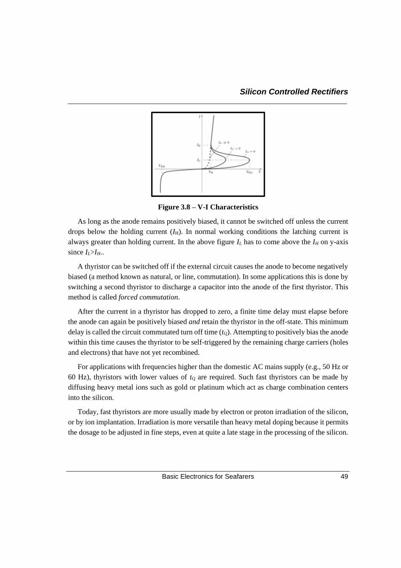
Figure 3.8 – V-I Characteristics
As long as the anode remains positively biased, it cannot be switched off unless the current
drops below the holding current (IH). In normal working conditions the latching current is
always greater than holding current. In the above figure IL has to come above the IH on y-axis
since IL>IH..
A thyristor can be switched off if the external circuit causes the anode to become negatively
biased (a method known as natural, or line, commutation). In some applications this is done by
switching a second thyristor to discharge a capacitor into the anode of the first thyristor. This
method is called forced commutation.
After the current in a thyristor has dropped to zero, a finite time delay must elapse before
the anode can again be positively biased and retain the thyristor in the off-state. This minimum
delay is called the circuit commutated turn off time (tQ). Attempting to positively bias the anode
within this time causes the thyristor to be self-triggered by the remaining charge carriers (holes
and electrons) that have not yet recombined.
For applications with frequencies higher than the domestic AC mains supply (e.g., 50 Hz or
60 Hz), thyristors with lower values of tQ are required. Such fast thyristors can be made by
diffusing heavy metal ions such as gold or platinum which act as charge combination centers
into the silicon.
Today, fast thyristors are more usually made by electron or proton irradiation of the silicon,
or by ion implantation. Irradiation is more versatile than heavy metal doping because it permits
the dosage to be adjusted in fine steps, even at quite a late stage in the processing of the silicon.
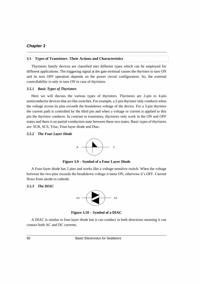
Chapter 3
Basic Electronics for Seafarers 50
3.5 Types of Transistors -Their Actions and Characteristics
Thyristors family devices are classified into different types which can be employed for
different applications. The triggering signal at the gate terminal causes the thyristor to turn ON
and its turn OFF operation depends on the power circuit configuration. So, the external
controllability is only to turn ON in case of thyristors
3.5.1 Basic Types of Thyristors
Here we will discuss the various types of thyristors. Thyristors are 2-pin to 4-pin
semiconductor devices that act like switches. For example, a 2-pin thyristor only conducts when
the voltage across its pins exceeds the breakdown voltage of the device. For a 3-pin thyristor
the current path is controlled by the third pin and when a voltage or current is applied to this
pin the thyristor conducts. In contrast to transistors, thyristors only work in the ON and OFF
states and there is no partial conduction state between these two states. Basic types of thyristors
are: SCR, SCS, Triac, Four-layer diode and Diac.
3.5.2 The Four Layer Diode
Figure 3.9 – Symbol of a Four Layer Diode
A Four-layer diode has 2 pins and works like a voltage-sensitive switch. When the voltage
between the two pins exceeds the breakdown voltage it turns ON, otherwise it’s OFF. Current
flows from anode to cathode.
3.5.3 The DIAC
Figure 3.10 – Symbol of a DIAC
A DIAC is similar to four-layer diode but it can conduct in both directions meaning it can
contact both AC and DC currents.
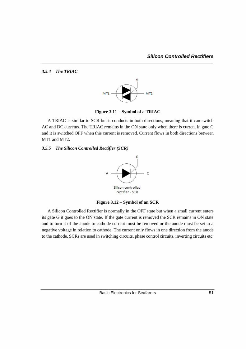
Silicon Controlled Rectifiers
Basic Electronics for Seafarers 51
3.5.4 The TRIAC
Figure 3.11 – Symbol of a TRIAC
A TRIAC is similar to SCR but it conducts in both directions, meaning that it can switch
AC and DC currents. The TRIAC remains in the ON state only when there is current in gate G
and it is switched OFF when this current is removed. Current flows in both directions between
MT1 and MT2.
3.5.5 The Silicon Controlled Rectifier (SCR)
Figure 3.12 – Symbol of an SCR
A Silicon Controlled Rectifier is normally in the OFF state but when a small current enters
its gate G it goes to the ON state. If the gate current is removed the SCR remains in ON state
and to turn it of the anode to cathode current must be removed or the anode must be set to a
negative voltage in relation to cathode. The current only flows in one direction from the anode
to the cathode. SCRs are used in switching circuits, phase control circuits, inverting circuits etc.
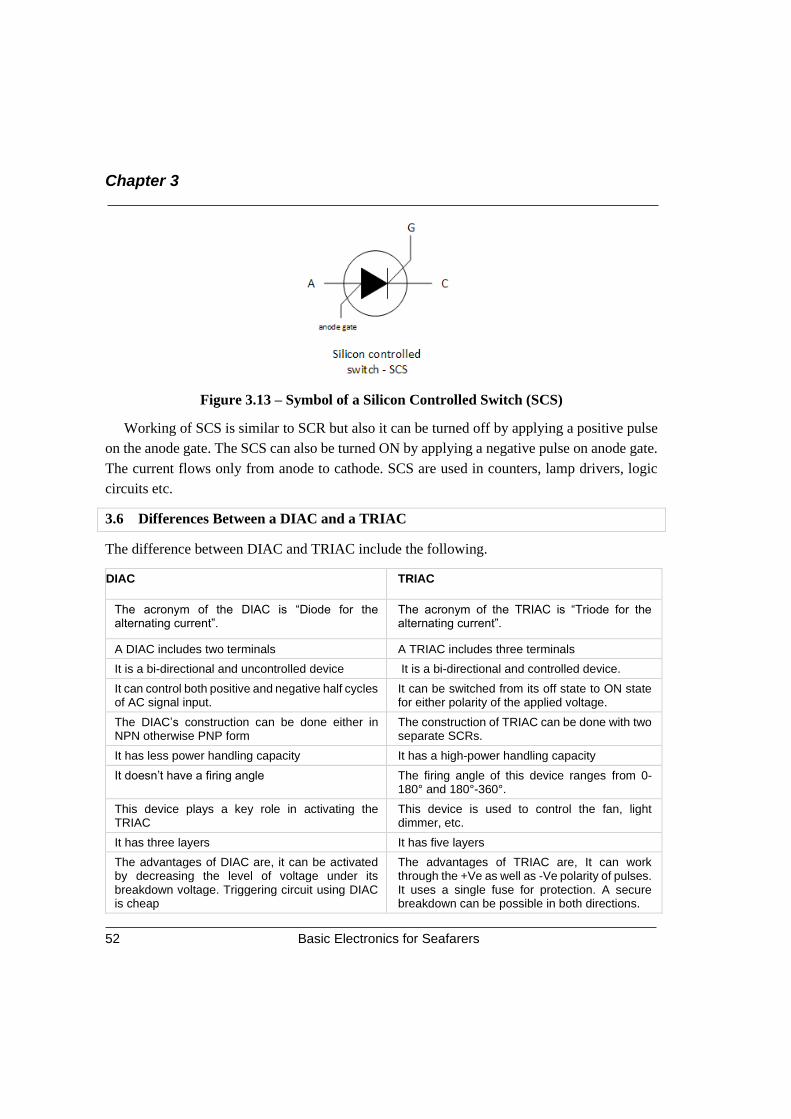
Chapter 3
Basic Electronics for Seafarers 52
Figure 3.13 – Symbol of a Silicon Controlled Switch (SCS)
Working of SCS is similar to SCR but also it can be turned off by applying a positive pulse
on the anode gate. The SCS can also be turned ON by applying a negative pulse on anode gate.
The current flows only from anode to cathode. SCS are used in counters, lamp drivers, logic
circuits etc.
3.6 Differences Between a DIAC and a TRIAC
The difference between DIAC and TRIAC include the following.
DIAC TRIAC
The acronym of the DIAC is “Diode for the alternating current”.
The acronym of the TRIAC is “Triode for the alternating current”.
A DIAC includes two terminals A TRIAC includes three terminals
It is a bi-directional and uncontrolled device It is a bi-directional and controlled device.
It can control both positive and negative half cycles of AC signal input.
It can be switched from its off state to ON state for either polarity of the applied voltage.
The DIAC’s construction can be done either in NPN otherwise PNP form
The construction of TRIAC can be done with two separate SCRs.
It has less power handling capacity It has a high-power handling capacity
It doesn’t have a firing angle The firing angle of this device ranges from 0-180° and 180°-360°.
This device plays a key role in activating the TRIAC
This device is used to control the fan, light dimmer, etc.
It has three layers It has five layers
The advantages of DIAC are, it can be activated by decreasing the level of voltage under its breakdown voltage. Triggering circuit using DIAC is cheap
The advantages of TRIAC are, It can work through the +Ve as well as -Ve polarity of pulses. It uses a single fuse for protection. A secure breakdown can be possible in both directions.
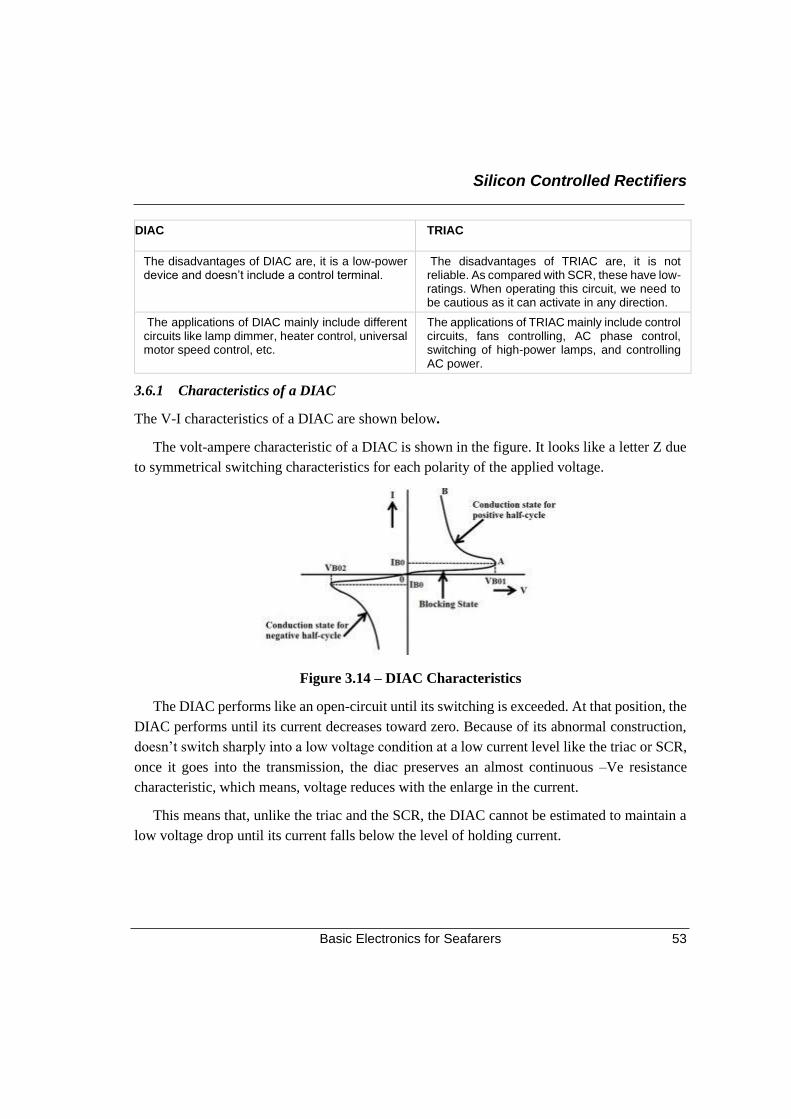
Silicon Controlled Rectifiers
Basic Electronics for Seafarers 53
DIAC TRIAC
The disadvantages of DIAC are, it is a low-power device and doesn’t include a control terminal.
The disadvantages of TRIAC are, it is not reliable. As compared with SCR, these have low- ratings. When operating this circuit, we need to be cautious as it can activate in any direction.
The applications of DIAC mainly include different circuits like lamp dimmer, heater control, universal motor speed control, etc.
The applications of TRIAC mainly include control circuits, fans controlling, AC phase control, switching of high-power lamps, and controlling AC power.
3.6.1 Characteristics of a DIAC
The V-I characteristics of a DIAC are shown below.
The volt-ampere characteristic of a DIAC is shown in the figure. It looks like a letter Z due
to symmetrical switching characteristics for each polarity of the applied voltage.
Figure 3.14 – DIAC Characteristics
The DIAC performs like an open-circuit until its switching is exceeded. At that position, the
DIAC performs until its current decreases toward zero. Because of its abnormal construction,
doesn’t switch sharply into a low voltage condition at a low current level like the triac or SCR,
once it goes into the transmission, the diac preserves an almost continuous –Ve resistance
characteristic, which means, voltage reduces with the enlarge in the current.
This means that, unlike the triac and the SCR, the DIAC cannot be estimated to maintain a
low voltage drop until its current falls below the level of holding current.
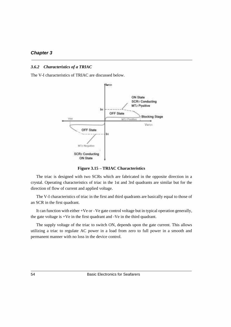
Chapter 3
Basic Electronics for Seafarers 54
3.6.2 Characteristics of a TRIAC
The V-I characteristics of TRIAC are discussed below.
Figure 3.15 – TRIAC Characteristics
The triac is designed with two SCRs which are fabricated in the opposite direction in a
crystal. Operating characteristics of triac in the 1st and 3rd quadrants are similar but for the
direction of flow of current and applied voltage.
The V-I characteristics of triac in the first and third quadrants are basically equal to those of
an SCR in the first quadrant.
It can function with either +Ve or –Ve gate control voltage but in typical operation generally,
the gate voltage is +Ve in the first quadrant and -Ve in the third quadrant.
The supply voltage of the triac to switch ON, depends upon the gate current. This allows
utilizing a triac to regulate AC power in a load from zero to full power in a smooth and
permanent manner with no loss in the device control.
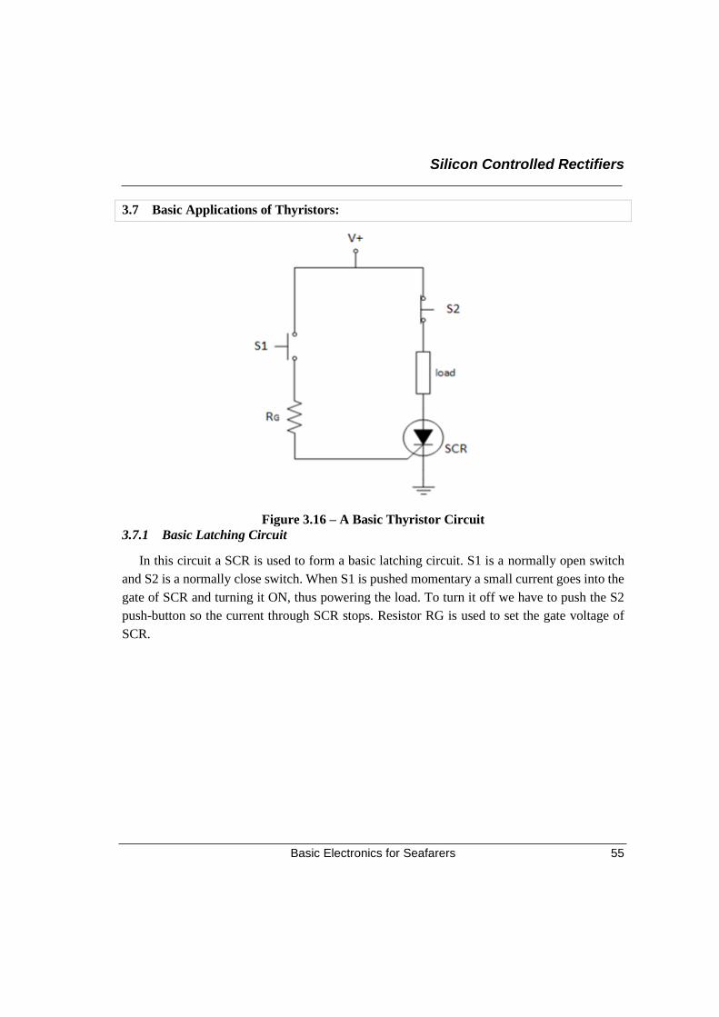
Silicon Controlled Rectifiers
Basic Electronics for Seafarers 55
3.7 Basic Applications of Thyristors:
Figure 3.16 – A Basic Thyristor Circuit
3.7.1 Basic Latching Circuit
In this circuit a SCR is used to form a basic latching circuit. S1 is a normally open switch
and S2 is a normally close switch. When S1 is pushed momentary a small current goes into the
gate of SCR and turning it ON, thus powering the load. To turn it off we have to push the S2
push-button so the current through SCR stops. Resistor RG is used to set the gate voltage of
SCR.
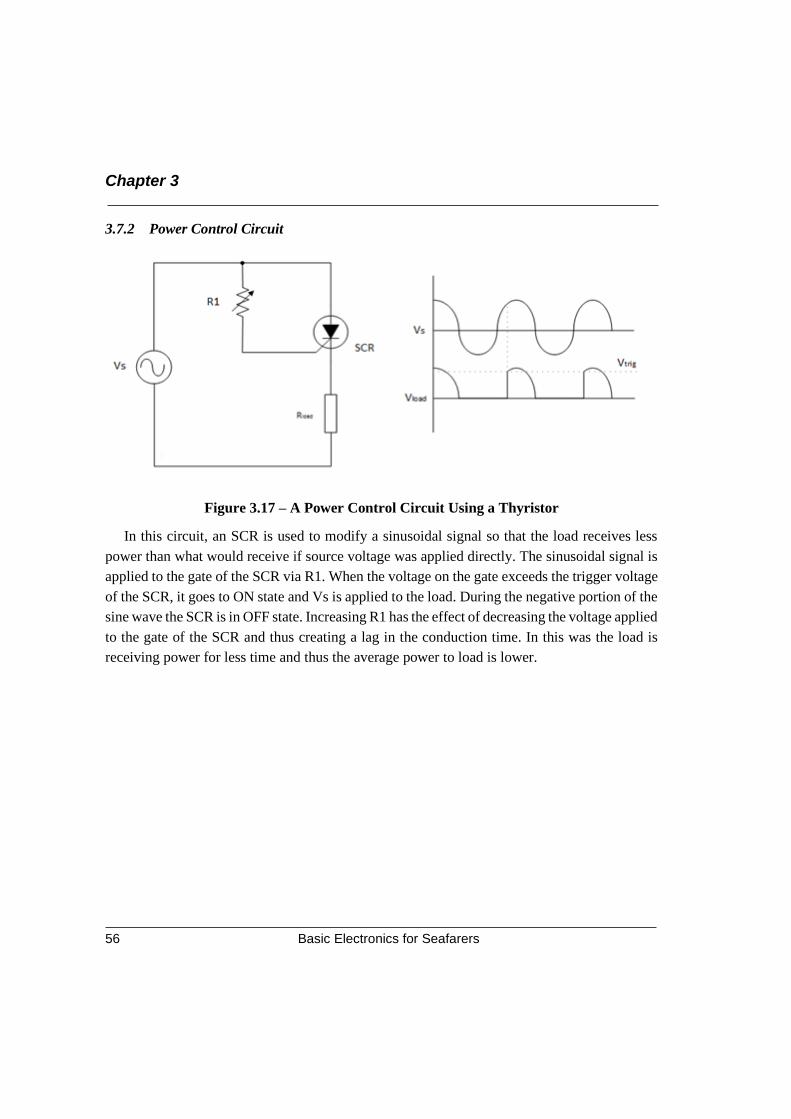
Chapter 3
Basic Electronics for Seafarers 56
3.7.2 Power Control Circuit
Figure 3.17 – A Power Control Circuit Using a Thyristor
In this circuit, an SCR is used to modify a sinusoidal signal so that the load receives less
power than what would receive if source voltage was applied directly. The sinusoidal signal is
applied to the gate of the SCR via R1. When the voltage on the gate exceeds the trigger voltage
of the SCR, it goes to ON state and Vs is applied to the load. During the negative portion of the
sine wave the SCR is in OFF state. Increasing R1 has the effect of decreasing the voltage applied
to the gate of the SCR and thus creating a lag in the conduction time. In this was the load is
receiving power for less time and thus the average power to load is lower.
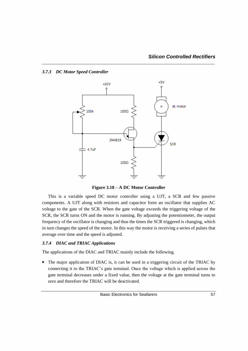
Silicon Controlled Rectifiers
Basic Electronics for Seafarers 57
3.7.3 DC Motor Speed Controller
Figure 3.18 – A DC Motor Controller
This is a variable speed DC motor controller using a UJT, a SCR and few passive
components. A UJT along with resistors and capacitor form an oscillator that supplies AC
voltage to the gate of the SCR. When the gate voltage exceeds the triggering voltage of the
SCR, the SCR turns ON and the motor is running. By adjusting the potentiometer, the output
frequency of the oscillator is changing and thus the times the SCR triggered is changing, which
in turn changes the speed of the motor. In this way the motor is receiving a series of pulses that
average over time and the speed is adjusted.
3.7.4 DIAC and TRIAC Applications
The applications of the DIAC and TRIAC mainly include the following.
• The major application of DIAC is, it can be used in a triggering circuit of the TRIAC by
connecting it to the TRIAC’s gate terminal. Once the voltage which is applied across the
gate terminal decreases under a fixed value, then the voltage at the gate terminal turns to
zero and therefore the TRIAC will be deactivated.
Chapter 3
Basic Electronics for Seafarers 58
• A DIAC is used to build different circuits like lamp dimmer, heat control, the universal
motor speed control circuit and starter circuits used in fluorescent lamps.
• A TRIAC is used in the control circuits such as motor control, fan speed controlling, light
dimmers, switching of high-power lamps, controlling of AC power in domestic applications.
3.7.5 Thyristor Applications
• Variable speed motor drives.
• Controlling high power electrical applications.
• AC motors, lights, welding machines etc.
• Fault current limiter and circuit breaker.
• Fast switching speed and low conduction is possible in eto thyristor.
• Light dimmers in television, movie theatres.
• Photography for flashes.
• Burglar alarms.
• Electric fan speed control.
• Car ignition switches.
3.7.6 Advantages of Thyristors
• Low cost.
• Can be protected with the help of fuse.
• Can handle large voltage/ current.
• Able to control AC power.
• Very easy to control.
• Easy to turn on.
• The GTO or Gate Turnoff Thyristor has high efficiency.
• Takes less time to operate.
• Thyristor switches can operate with large frequency.
• Requires less space when compared to mechanical switches.
Silicon Controlled Rectifiers
Basic Electronics for Seafarers 59
• Can be used for robust operations.
• Maintenance cost of Thyristor is very less.
• Very easy to use for sophisticated controlling.
• Power handling capacity is very good.
• Can be used as an oscillator in digital circuits.
• Can be connected in parallel and in series to provide electronic control at high power levels.
• Thyristors conduct current only in one direction.
• It can be used as a protection device, like a fuse in a power line.
3.7.7 Disadvantages of Thyristors
• The disadvantages of Thyristor include:
- Cannot be used for higher frequencies.
- In AC circuit, Thyristor needs to be turned on each cycle.
- SCR takes time to turn on and off. This causes delay or damage in the load.
- It can stop the motor when connected, but cannot hold it stationary.
- The response rate of Thyristor is very low.
- Not much use in DC circuits, as the Thyristor cannot be cutoff just by removing the
gate drive.
- Low Efficiency.
- Latching and Holding current is more in GTO Thyristor.
- Reverse blocking capability of voltage is less than forward blocking capability.
- Reliability of TRIAC thyristor is less than SCR.
- TRIACs have lower dv/dt rating when compared to SCR.

Chapter 3
Basic Electronics for Seafarers 60
Sources
• circuitdigest.com
• Wikipedia.com
• electronicshub.com
• electronicslab.com
• elprocus.com
• electricalfundablog.com
WOW! By reading this chapter, all my doubts
about thyristor got cleared. Thank You Sir.
For making this content so interesting and
easy to understand. I hope that all the
readers also must have also got clarity about
these topics and understood the importance
of thyristor in electronics as well as
electrical circuits!
Divyam! Patience is necessary,
and one cannot reap
immediately where one has
sown. Thank You!

Chapter 4 Power Electronics
Basic Electronics for Seafarers
Sir, I am gaining confidence as
I progress through these
chapters! They help me to clear
my basics of Electronics that
are going to be of use in real
time.
Divyam my boy, I feel happy to know
this! Though it is not the last chapter
of this book, remember that there is
no end to knowledge. As Steve Jobs
said “STAY HUNGRY STAY
FOOLISH”. Be always ready to learn.
In this chapter I’m going to brief you
about Power Electronics. Power
electronics is the application of solid-
state electronics to the control and
conversion of electric power. Now
follow me!
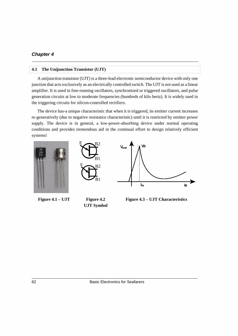
Chapter 4
Basic Electronics for Seafarers 62
4.1 The Unijunction Transistor (UJT)
A unijunction transistor (UJT) is a three-lead electronic semiconductor device with only one
junction that acts exclusively as an electrically controlled switch. The UJT is not used as a linear
amplifier. It is used in free-running oscillators, synchronized or triggered oscillators, and pulse
generation circuits at low to moderate frequencies (hundreds of kilo hertz). It is widely used in
the triggering circuits for silicon-controlled rectifiers.
The device has-a unique characteristic that when it is triggered, its emitter current increases
re-generatively (due to negative resistance characteristic) until it is restricted by emitter power
supply. The device is in general, a low-power-absorbing device under normal operating
conditions and provides tremendous aid in the continual effort to design relatively efficient
systems!
Figure 4.1 – UJT Figure 4.2
UJT Symbol
Figure 4.3 – UJT Characteristics
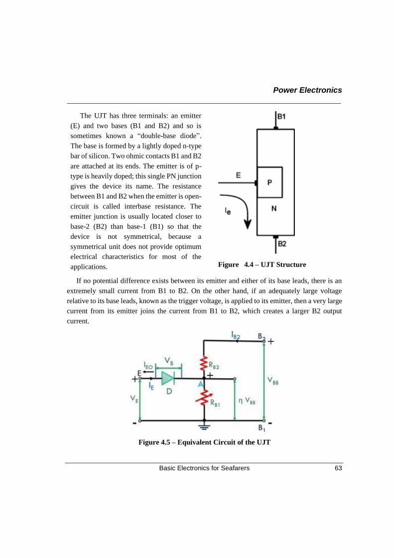
Power Electronics
Basic Electronics for Seafarers 63
The UJT has three terminals: an emitter
(E) and two bases (B1 and B2) and so is
sometimes known a “double-base diode”.
The base is formed by a lightly doped n-type
bar of silicon. Two ohmic contacts B1 and B2
are attached at its ends. The emitter is of p-
type is heavily doped; this single PN junction
gives the device its name. The resistance
between B1 and B2 when the emitter is open-
circuit is called interbase resistance. The
emitter junction is usually located closer to
base-2 (B2) than base-1 (B1) so that the
device is not symmetrical, because a
symmetrical unit does not provide optimum
electrical characteristics for most of the
applications.
Figure 4.4 – UJT Structure
If no potential difference exists between its emitter and either of its base leads, there is an
extremely small current from B1 to B2. On the other hand, if an adequately large voltage
relative to its base leads, known as the trigger voltage, is applied to its emitter, then a very large
current from its emitter joins the current from B1 to B2, which creates a larger B2 output
current.
Figure 4.5 – Equivalent Circuit of the UJT
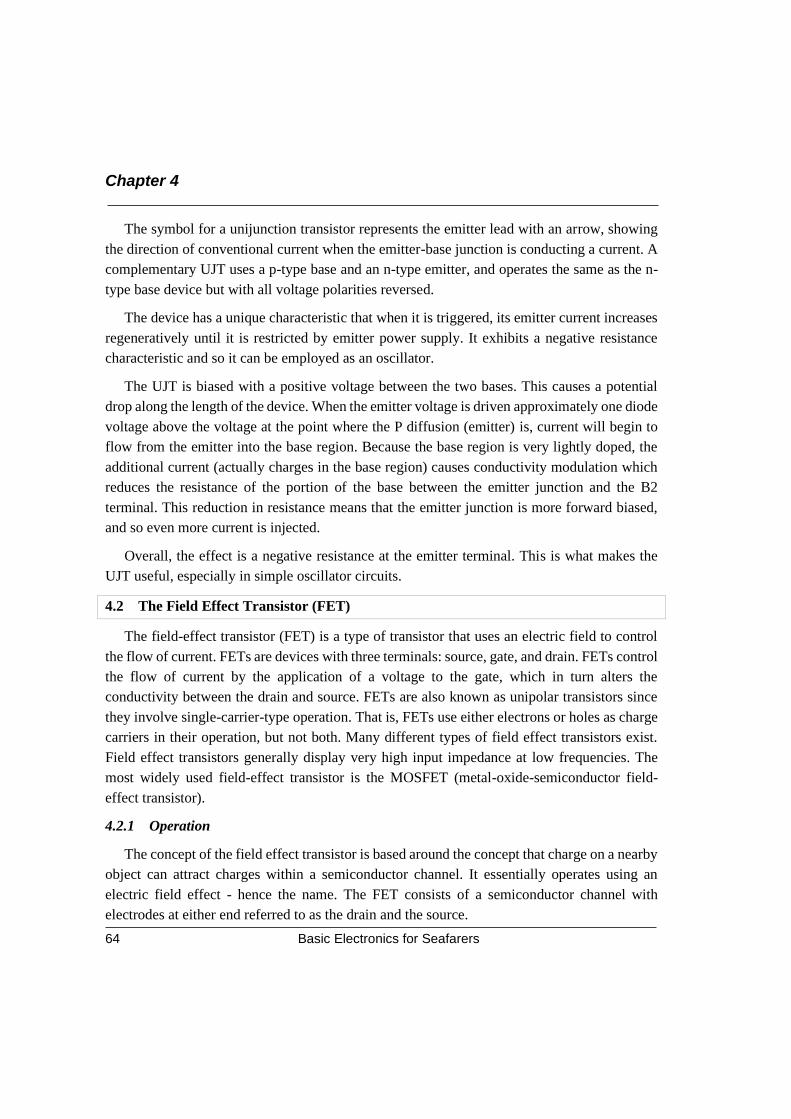
Chapter 4
Basic Electronics for Seafarers 64
The symbol for a unijunction transistor represents the emitter lead with an arrow, showing
the direction of conventional current when the emitter-base junction is conducting a current. A
complementary UJT uses a p-type base and an n-type emitter, and operates the same as the n-
type base device but with all voltage polarities reversed.
The device has a unique characteristic that when it is triggered, its emitter current increases
regeneratively until it is restricted by emitter power supply. It exhibits a negative resistance
characteristic and so it can be employed as an oscillator.
The UJT is biased with a positive voltage between the two bases. This causes a potential
drop along the length of the device. When the emitter voltage is driven approximately one diode
voltage above the voltage at the point where the P diffusion (emitter) is, current will begin to
flow from the emitter into the base region. Because the base region is very lightly doped, the
additional current (actually charges in the base region) causes conductivity modulation which
reduces the resistance of the portion of the base between the emitter junction and the B2
terminal. This reduction in resistance means that the emitter junction is more forward biased,
and so even more current is injected.
Overall, the effect is a negative resistance at the emitter terminal. This is what makes the
UJT useful, especially in simple oscillator circuits.
4.2 The Field Effect Transistor (FET)
The field-effect transistor (FET) is a type of transistor that uses an electric field to control
the flow of current. FETs are devices with three terminals: source, gate, and drain. FETs control
the flow of current by the application of a voltage to the gate, which in turn alters the
conductivity between the drain and source. FETs are also known as unipolar transistors since
they involve single-carrier-type operation. That is, FETs use either electrons or holes as charge
carriers in their operation, but not both. Many different types of field effect transistors exist.
Field effect transistors generally display very high input impedance at low frequencies. The
most widely used field-effect transistor is the MOSFET (metal-oxide-semiconductor field-
effect transistor).
4.2.1 Operation
The concept of the field effect transistor is based around the concept that charge on a nearby
object can attract charges within a semiconductor channel. It essentially operates using an
electric field effect - hence the name. The FET consists of a semiconductor channel with
electrodes at either end referred to as the drain and the source.
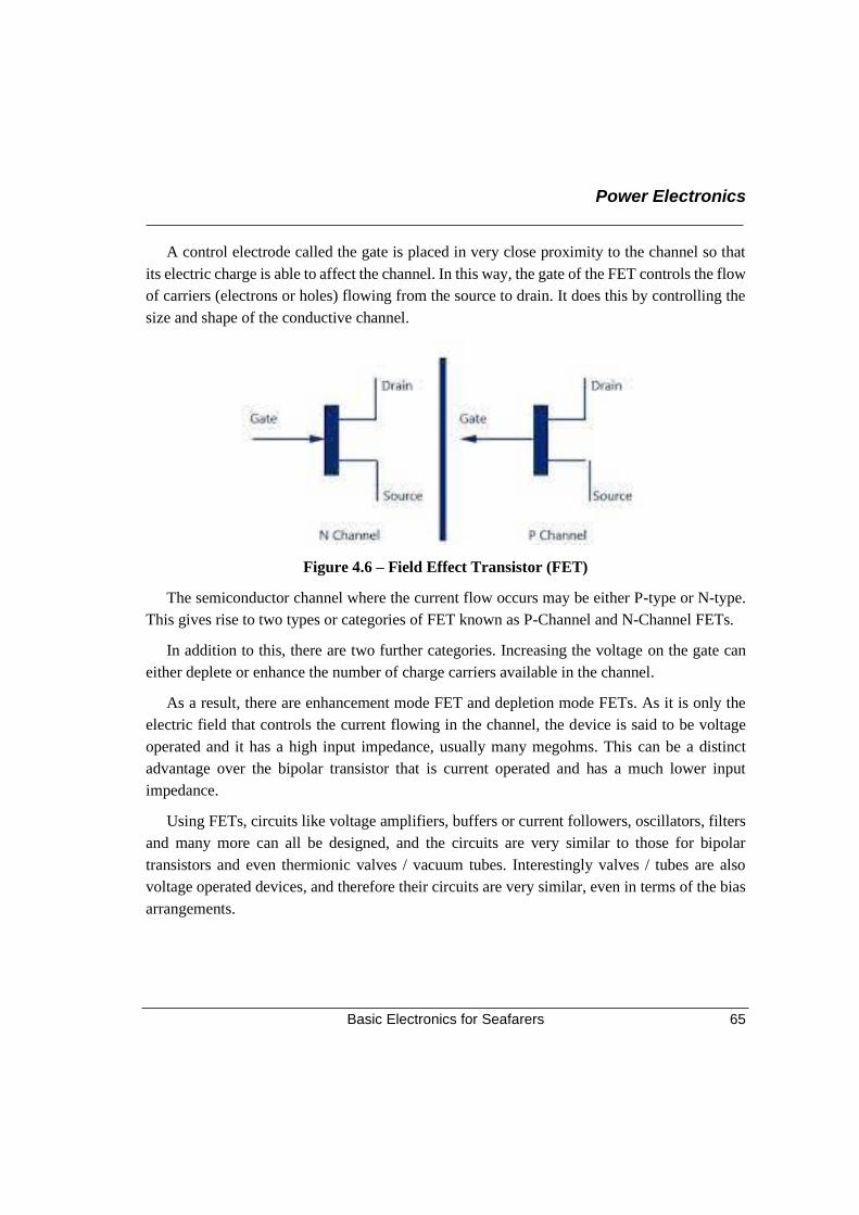
Power Electronics
Basic Electronics for Seafarers 65
A control electrode called the gate is placed in very close proximity to the channel so that
its electric charge is able to affect the channel. In this way, the gate of the FET controls the flow
of carriers (electrons or holes) flowing from the source to drain. It does this by controlling the
size and shape of the conductive channel.
Figure 4.6 – Field Effect Transistor (FET)
The semiconductor channel where the current flow occurs may be either P-type or N-type.
This gives rise to two types or categories of FET known as P-Channel and N-Channel FETs.
In addition to this, there are two further categories. Increasing the voltage on the gate can
either deplete or enhance the number of charge carriers available in the channel.
As a result, there are enhancement mode FET and depletion mode FETs. As it is only the
electric field that controls the current flowing in the channel, the device is said to be voltage
operated and it has a high input impedance, usually many megohms. This can be a distinct
advantage over the bipolar transistor that is current operated and has a much lower input
impedance.
Using FETs, circuits like voltage amplifiers, buffers or current followers, oscillators, filters
and many more can all be designed, and the circuits are very similar to those for bipolar
transistors and even thermionic valves / vacuum tubes. Interestingly valves / tubes are also
voltage operated devices, and therefore their circuits are very similar, even in terms of the bias
arrangements.
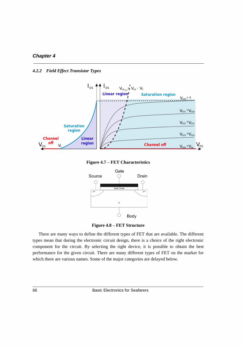
Chapter 4
Basic Electronics for Seafarers 66
4.2.2 Field Effect Transistor Types
Figure 4.7 – FET Characteristics
Figure 4.8 – FET Structure
There are many ways to define the different types of FET that are available. The different
types mean that during the electronic circuit design, there is a choice of the right electronic
component for the circuit. By selecting the right device, it is possible to obtain the best
performance for the given circuit. There are many different types of FET on the market for
which there are various names. Some of the major categories are delayed below.

Power Electronics
Basic Electronics for Seafarers 67
• Junction FET, JFET The junction FET, or JFET uses a reverse biased diode junction to
provide the gate connection. The structure consists of a semiconductor channel which can
be either N-type or P-type. A semiconductor diode is then fabricated onto the channel in
such a way that the voltage on the diode affects the FET channel. In operation this is reverse
biased and this means that it is effectively isolated from the channel - only the diode reverse
current can flow between the two. The JFET is the most basic type of FET, and the one that
was first developed. However, it still provides excellent service in many areas of electronics.
• Insulated Gate FET / Metal Oxide Silicon FET MOSFET: The MOSFET uses an
insulated layer between the gate and the channel. Typically, this is formed from a layer of
oxide of the semiconductor. The name IGFET refers to any type of FET that has an insulated
gate. The most common form of IGFET is the silicon MOSFET - Metal Oxide Silicon FET.
Here, the gate is made of a layer of metal set down on the silicon oxide which in turn is on
the silicon channel. MOSFETs are widely used in many areas of electronics and particularly
within integrated circuits. The key factor of the IGFET / MOSFET is the exceedingly gate
high impedance these FETs are able to provide. That said, there will be an associated
capacitance and this will reduce the input impedance as the frequency rises.
• Dual Gate MOSFET This is a specialised form of MOSFET that has two gates in series
along the channel. This enables some considerable performance improvements to be made,
especially at RF, when compared to single gate devices. The second gate of the MOSFET
provides additional isolation between the input and output, and in addition to this it can be
used in applications like mixing / multiplication.
• MESFET The MEtal Silicon FET is normally fabricated using Gallium Arsenide and is
often referred to as a GaAs FET. Often GaAsFETs are used for RF applications where they
can provide high gain low noise performance. One of the drawbacks of GaAsFET
technology results from the very small gate structure, and this makes its very sensitive to
damage from static, ESD. Great care must be taken when handling these devices.
• HEMT / PHEMT The High Electron Mobility Transistor and Pseudomorphic High
Electron Mobility Transistor are developments of the basic FET concept, but developed to
enable very high frequency operation. Although expensive, they enable very high
frequencies and high levels of performance to be achieved.
• FinFET FinFET technology is now being used within integrated circuits to enable higher
levels of integration to be achieved by allowing smaller feature sizes.
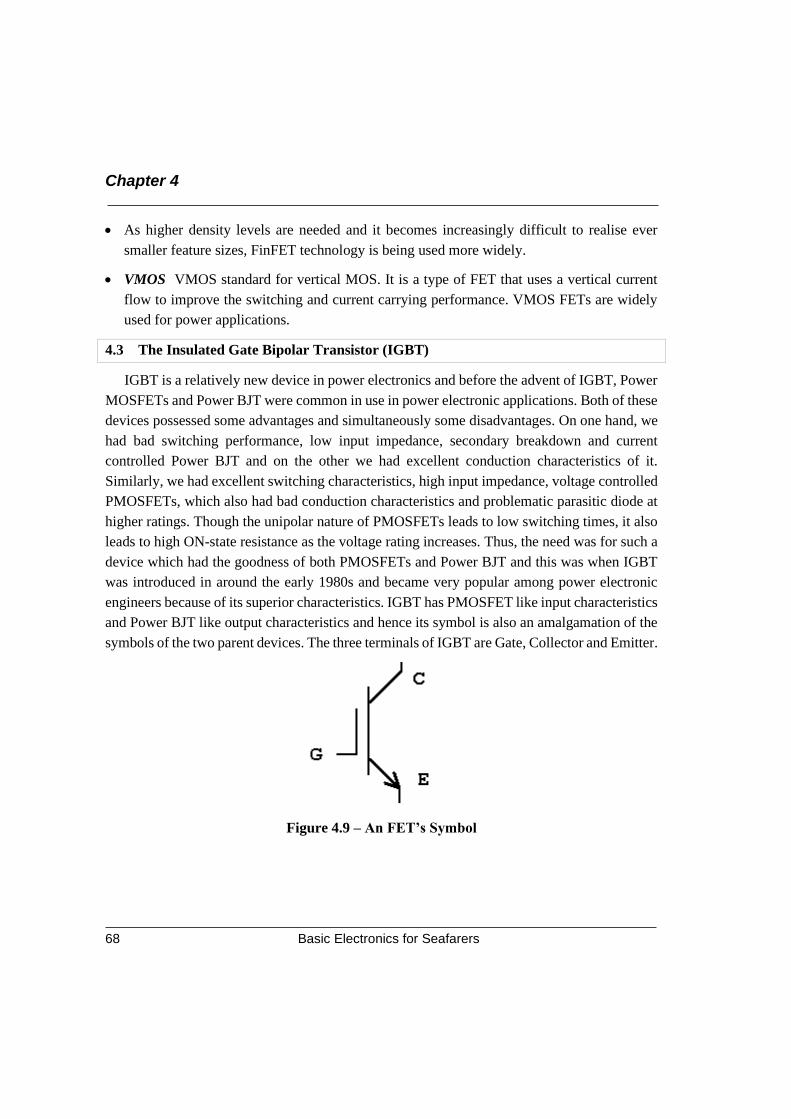
Chapter 4
Basic Electronics for Seafarers 68
• As higher density levels are needed and it becomes increasingly difficult to realise ever
smaller feature sizes, FinFET technology is being used more widely.
• VMOS VMOS standard for vertical MOS. It is a type of FET that uses a vertical current
flow to improve the switching and current carrying performance. VMOS FETs are widely
used for power applications.
4.3 The Insulated Gate Bipolar Transistor (IGBT)
IGBT is a relatively new device in power electronics and before the advent of IGBT, Power
MOSFETs and Power BJT were common in use in power electronic applications. Both of these
devices possessed some advantages and simultaneously some disadvantages. On one hand, we
had bad switching performance, low input impedance, secondary breakdown and current
controlled Power BJT and on the other we had excellent conduction characteristics of it.
Similarly, we had excellent switching characteristics, high input impedance, voltage controlled
PMOSFETs, which also had bad conduction characteristics and problematic parasitic diode at
higher ratings. Though the unipolar nature of PMOSFETs leads to low switching times, it also
leads to high ON-state resistance as the voltage rating increases. Thus, the need was for such a
device which had the goodness of both PMOSFETs and Power BJT and this was when IGBT
was introduced in around the early 1980s and became very popular among power electronic
engineers because of its superior characteristics. IGBT has PMOSFET like input characteristics
and Power BJT like output characteristics and hence its symbol is also an amalgamation of the
symbols of the two parent devices. The three terminals of IGBT are Gate, Collector and Emitter.
Figure 4.9 – An FET’s Symbol
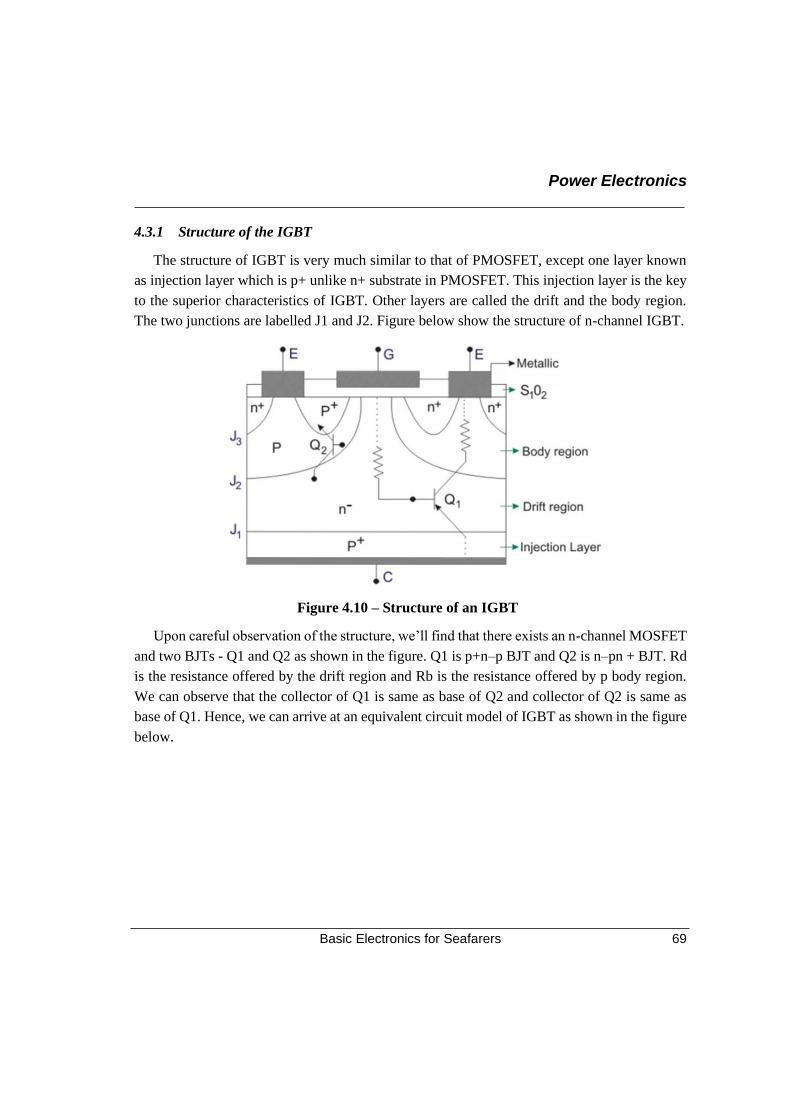
Power Electronics
Basic Electronics for Seafarers 69
4.3.1 Structure of the IGBT
The structure of IGBT is very much similar to that of PMOSFET, except one layer known
as injection layer which is p+ unlike n+ substrate in PMOSFET. This injection layer is the key
to the superior characteristics of IGBT. Other layers are called the drift and the body region.
The two junctions are labelled J1 and J2. Figure below show the structure of n-channel IGBT.
Figure 4.10 – Structure of an IGBT
Upon careful observation of the structure, we’ll find that there exists an n-channel MOSFET
and two BJTs - Q1 and Q2 as shown in the figure. Q1 is p+n–p BJT and Q2 is n–pn + BJT. Rd
is the resistance offered by the drift region and Rb is the resistance offered by p body region.
We can observe that the collector of Q1 is same as base of Q2 and collector of Q2 is same as
base of Q1. Hence, we can arrive at an equivalent circuit model of IGBT as shown in the figure
below.
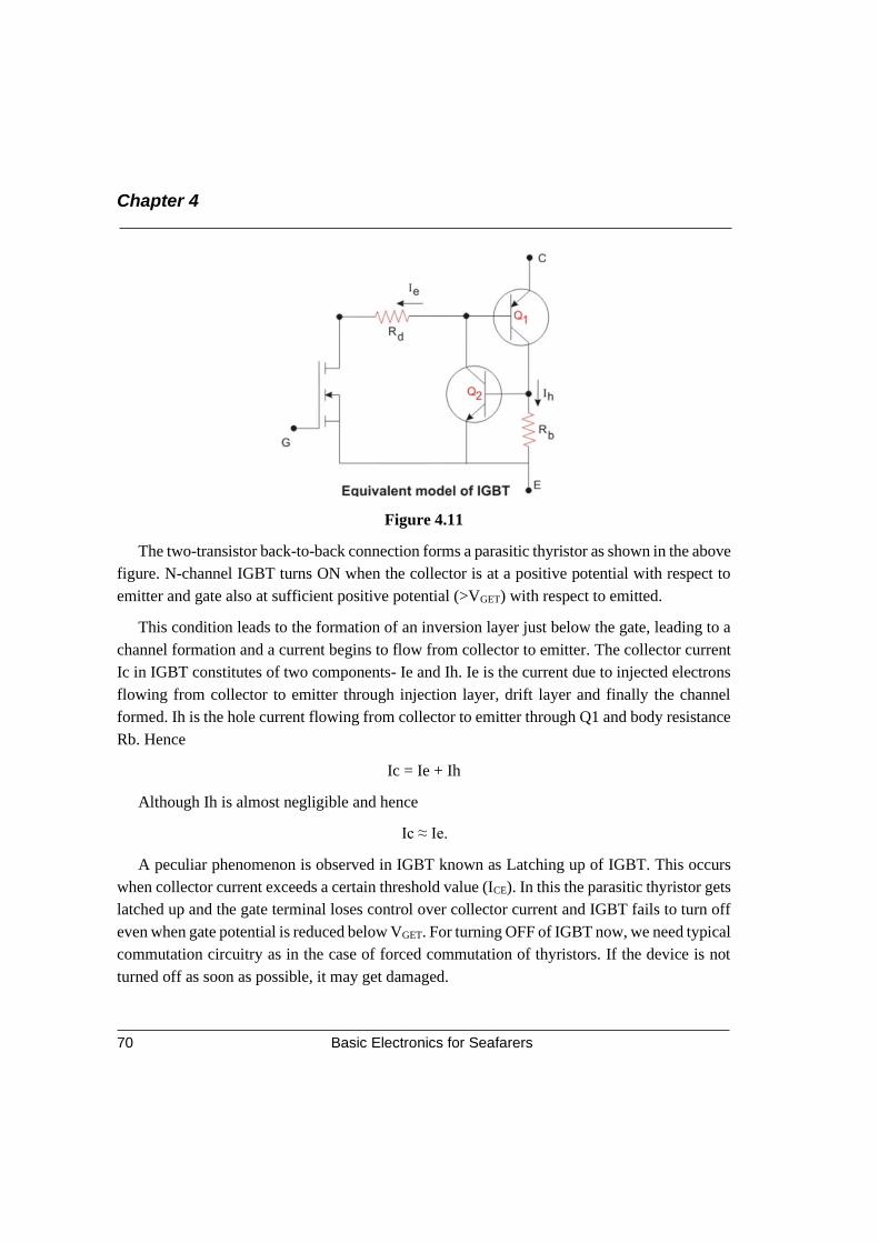
Chapter 4
Basic Electronics for Seafarers 70
Figure 4.11
The two-transistor back-to-back connection forms a parasitic thyristor as shown in the above
figure. N-channel IGBT turns ON when the collector is at a positive potential with respect to
emitter and gate also at sufficient positive potential (>VGET) with respect to emitted.
This condition leads to the formation of an inversion layer just below the gate, leading to a
channel formation and a current begins to flow from collector to emitter. The collector current
Ic in IGBT constitutes of two components- Ie and Ih. Ie is the current due to injected electrons
flowing from collector to emitter through injection layer, drift layer and finally the channel
formed. Ih is the hole current flowing from collector to emitter through Q1 and body resistance
Rb. Hence
Ic = Ie + Ih
Although Ih is almost negligible and hence
Ic ≈ Ie.
A peculiar phenomenon is observed in IGBT known as Latching up of IGBT. This occurs
when collector current exceeds a certain threshold value (ICE). In this the parasitic thyristor gets
latched up and the gate terminal loses control over collector current and IGBT fails to turn off
even when gate potential is reduced below VGET. For turning OFF of IGBT now, we need typical
commutation circuitry as in the case of forced commutation of thyristors. If the device is not
turned off as soon as possible, it may get damaged.
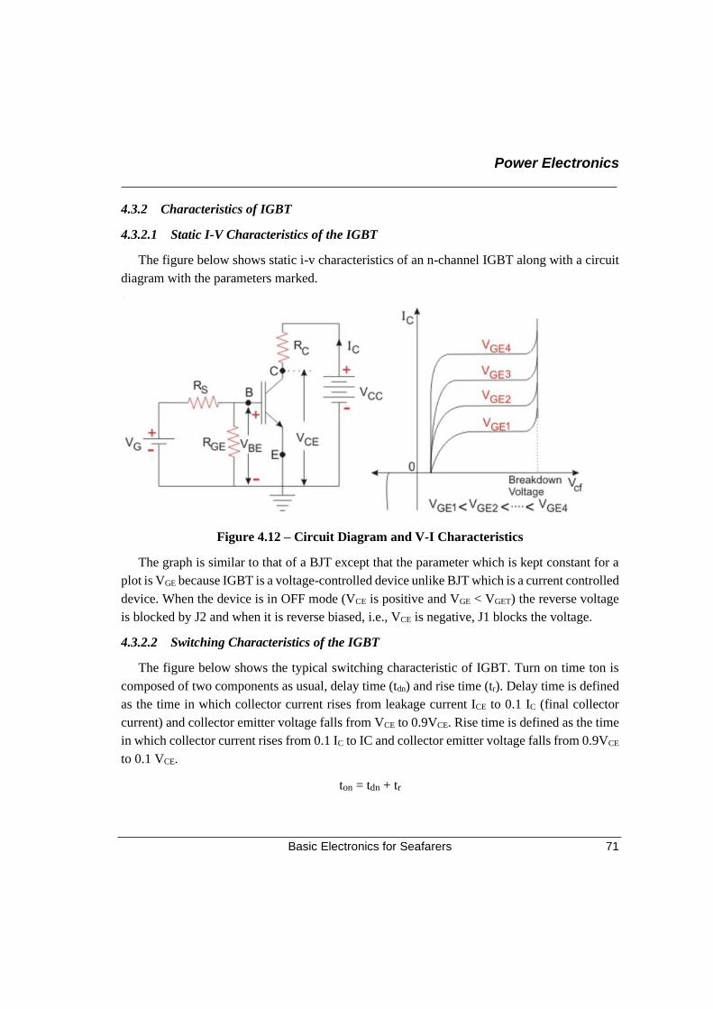
Power Electronics
Basic Electronics for Seafarers 71
4.3.2 Characteristics of IGBT
4.3.2.1 Static I-V Characteristics of the IGBT
The figure below shows static i-v characteristics of an n-channel IGBT along with a circuit
diagram with the parameters marked.
Figure 4.12 – Circuit Diagram and V-I Characteristics
The graph is similar to that of a BJT except that the parameter which is kept constant for a
plot is VGE because IGBT is a voltage-controlled device unlike BJT which is a current controlled
device. When the device is in OFF mode (VCE is positive and VGE < VGET) the reverse voltage
is blocked by J2 and when it is reverse biased, i.e., VCE is negative, J1 blocks the voltage.
4.3.2.2 Switching Characteristics of the IGBT
The figure below shows the typical switching characteristic of IGBT. Turn on time ton is
composed of two components as usual, delay time (tdn) and rise time (tr). Delay time is defined
as the time in which collector current rises from leakage current ICE to 0.1 IC (final collector
current) and collector emitter voltage falls from VCE to 0.9VCE. Rise time is defined as the time
in which collector current rises from 0.1 IC to IC and collector emitter voltage falls from 0.9VCE
to 0.1 VCE.
ton = tdn + tr
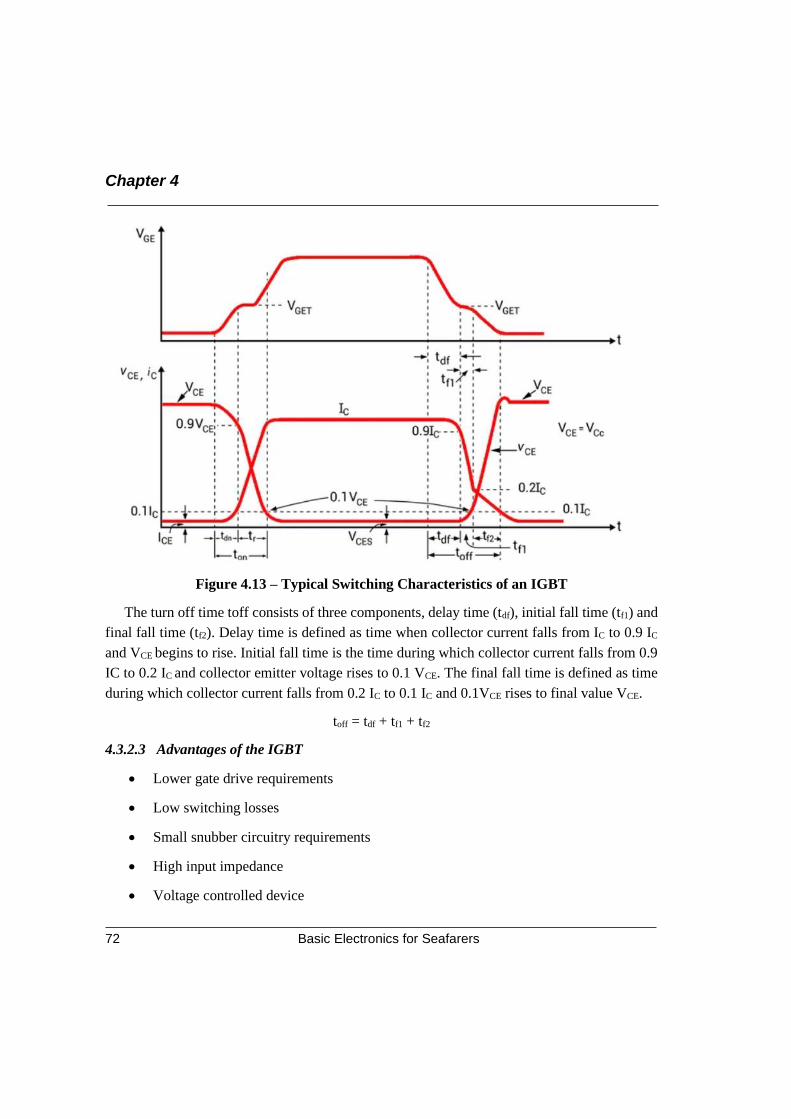
Chapter 4
Basic Electronics for Seafarers 72
Figure 4.13 – Typical Switching Characteristics of an IGBT
The turn off time toff consists of three components, delay time (tdf), initial fall time (tf1) and
final fall time (tf2). Delay time is defined as time when collector current falls from IC to 0.9 IC
and VCE begins to rise. Initial fall time is the time during which collector current falls from 0.9
IC to 0.2 IC and collector emitter voltage rises to 0.1 VCE. The final fall time is defined as time
during which collector current falls from 0.2 IC to 0.1 IC and 0.1VCE rises to final value VCE.
toff = tdf + tf1 + tf2
4.3.2.3 Advantages of the IGBT
• Lower gate drive requirements
• Low switching losses
• Small snubber circuitry requirements
• High input impedance
• Voltage controlled device
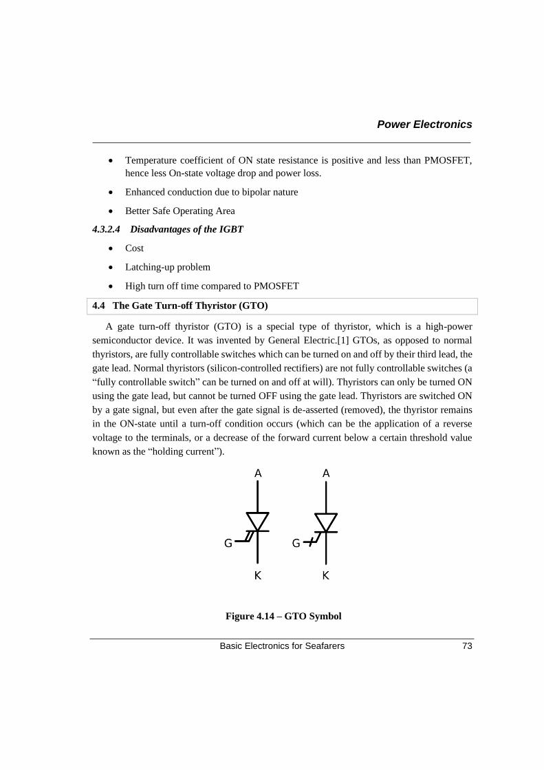
Power Electronics
Basic Electronics for Seafarers 73
• Temperature coefficient of ON state resistance is positive and less than PMOSFET,
hence less On-state voltage drop and power loss.
• Enhanced conduction due to bipolar nature
• Better Safe Operating Area
4.3.2.4 Disadvantages of the IGBT
• Cost
• Latching-up problem
• High turn off time compared to PMOSFET
4.4 The Gate Turn-off Thyristor (GTO)
A gate turn-off thyristor (GTO) is a special type of thyristor, which is a high-power
semiconductor device. It was invented by General Electric.[1] GTOs, as opposed to normal
thyristors, are fully controllable switches which can be turned on and off by their third lead, the
gate lead. Normal thyristors (silicon-controlled rectifiers) are not fully controllable switches (a
“fully controllable switch” can be turned on and off at will). Thyristors can only be turned ON
using the gate lead, but cannot be turned OFF using the gate lead. Thyristors are switched ON
by a gate signal, but even after the gate signal is de-asserted (removed), the thyristor remains
in the ON-state until a turn-off condition occurs (which can be the application of a reverse
voltage to the terminals, or a decrease of the forward current below a certain threshold value
known as the “holding current”).
Figure 4.14 – GTO Symbol
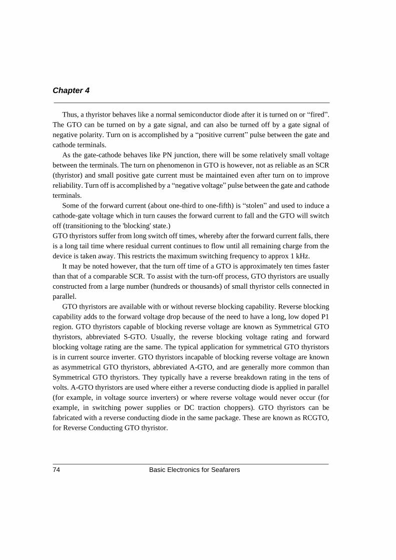
Chapter 4
Basic Electronics for Seafarers 74
Thus, a thyristor behaves like a normal semiconductor diode after it is turned on or “fired”.
The GTO can be turned on by a gate signal, and can also be turned off by a gate signal of
negative polarity. Turn on is accomplished by a “positive current” pulse between the gate and
cathode terminals.
As the gate-cathode behaves like PN junction, there will be some relatively small voltage
between the terminals. The turn on phenomenon in GTO is however, not as reliable as an SCR
(thyristor) and small positive gate current must be maintained even after turn on to improve
reliability. Turn off is accomplished by a “negative voltage” pulse between the gate and cathode
terminals.
Some of the forward current (about one-third to one-fifth) is “stolen” and used to induce a
cathode-gate voltage which in turn causes the forward current to fall and the GTO will switch
off (transitioning to the 'blocking' state.)
GTO thyristors suffer from long switch off times, whereby after the forward current falls, there
is a long tail time where residual current continues to flow until all remaining charge from the
device is taken away. This restricts the maximum switching frequency to approx 1 kHz.
It may be noted however, that the turn off time of a GTO is approximately ten times faster
than that of a comparable SCR. To assist with the turn-off process, GTO thyristors are usually
constructed from a large number (hundreds or thousands) of small thyristor cells connected in
parallel.
GTO thyristors are available with or without reverse blocking capability. Reverse blocking
capability adds to the forward voltage drop because of the need to have a long, low doped P1
region. GTO thyristors capable of blocking reverse voltage are known as Symmetrical GTO
thyristors, abbreviated S-GTO. Usually, the reverse blocking voltage rating and forward
blocking voltage rating are the same. The typical application for symmetrical GTO thyristors
is in current source inverter. GTO thyristors incapable of blocking reverse voltage are known
as asymmetrical GTO thyristors, abbreviated A-GTO, and are generally more common than
Symmetrical GTO thyristors. They typically have a reverse breakdown rating in the tens of
volts. A-GTO thyristors are used where either a reverse conducting diode is applied in parallel
(for example, in voltage source inverters) or where reverse voltage would never occur (for
example, in switching power supplies or DC traction choppers). GTO thyristors can be
fabricated with a reverse conducting diode in the same package. These are known as RCGTO,
for Reverse Conducting GTO thyristor.
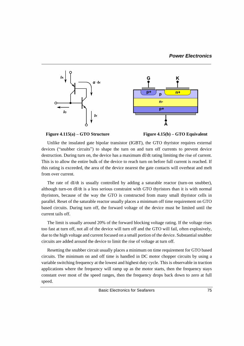
Power Electronics
Basic Electronics for Seafarers 75
Figure 4.115(a) – GTO Structure Figure 4.15(b) – GTO Equivalent
Unlike the insulated gate bipolar transistor (IGBT), the GTO thyristor requires external
devices (“snubber circuits”) to shape the turn on and turn off currents to prevent device
destruction. During turn on, the device has a maximum dI/dt rating limiting the rise of current.
This is to allow the entire bulk of the device to reach turn on before full current is reached. If
this rating is exceeded, the area of the device nearest the gate contacts will overheat and melt
from over current.
The rate of dI/dt is usually controlled by adding a saturable reactor (turn-on snubber),
although turn-on dI/dt is a less serious constraint with GTO thyristors than it is with normal
thyristors, because of the way the GTO is constructed from many small thyristor cells in
parallel. Reset of the saturable reactor usually places a minimum off time requirement on GTO
based circuits. During turn off, the forward voltage of the device must be limited until the
current tails off.
The limit is usually around 20% of the forward blocking voltage rating. If the voltage rises
too fast at turn off, not all of the device will turn off and the GTO will fail, often explosively,
due to the high voltage and current focused on a small portion of the device. Substantial snubber
circuits are added around the device to limit the rise of voltage at turn off.
Resetting the snubber circuit usually places a minimum on time requirement for GTO based
circuits. The minimum on and off time is handled in DC motor chopper circuits by using a
variable switching frequency at the lowest and highest duty cycle. This is observable in traction
applications where the frequency will ramp up as the motor starts, then the frequency stays
constant over most of the speed ranges, then the frequency drops back down to zero at full
speed.
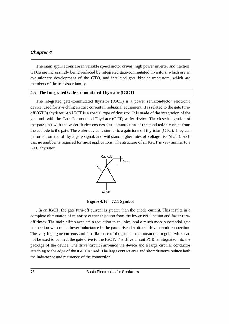
Chapter 4
Basic Electronics for Seafarers 76
The main applications are in variable speed motor drives, high power inverter and traction.
GTOs are increasingly being replaced by integrated gate-commutated thyristors, which are an
evolutionary development of the GTO, and insulated gate bipolar transistors, which are
members of the transistor family.
4.5 The Integrated Gate-Commutated Thyristor (IGCT)
The integrated gate-commutated thyristor (IGCT) is a power semiconductor electronic
device, used for switching electric current in industrial equipment. It is related to the gate turn-
off (GTO) thyristor. An IGCT is a special type of thyristor. It is made of the integration of the
gate unit with the Gate Commutated Thyristor (GCT) wafer device. The close integration of
the gate unit with the wafer device ensures fast commutation of the conduction current from
the cathode to the gate. The wafer device is similar to a gate turn-off thyristor (GTO). They can
be turned on and off by a gate signal, and withstand higher rates of voltage rise (dv/dt), such
that no snubber is required for most applications. The structure of an IGCT is very similar to a
GTO thyristor
Figure 4.16 – 7.11 Symbol
. In an IGCT, the gate turn-off current is greater than the anode current. This results in a
complete elimination of minority carrier injection from the lower PN junction and faster turn-
off times. The main differences are a reduction in cell size, and a much more substantial gate
connection with much lower inductance in the gate drive circuit and drive circuit connection.
The very high gate currents and fast dI/dt rise of the gate current mean that regular wires can
not be used to connect the gate drive to the IGCT. The drive circuit PCB is integrated into the
package of the device. The drive circuit surrounds the device and a large circular conductor
attaching to the edge of the IGCT is used. The large contact area and short distance reduce both
the inductance and resistance of the connection.
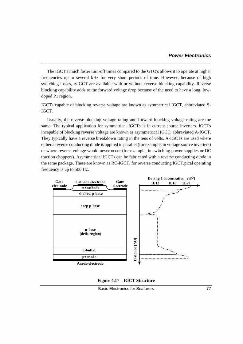
Power Electronics
Basic Electronics for Seafarers 77
The IGCT's much faster turn-off times compared to the GTO's allows it to operate at higher
frequencies up to several kHz for very short periods of time. However, because of high
switching losses, tyIGCT are available with or without reverse blocking capability. Reverse
blocking capability adds to the forward voltage drop because of the need to have a long, low-
doped P1 region.
IGCTs capable of blocking reverse voltage are known as symmetrical IGCT, abbreviated S-
IGCT.
Usually, the reverse blocking voltage rating and forward blocking voltage rating are the
same. The typical application for symmetrical IGCTs is in current source inverters. IGCTs
incapable of blocking reverse voltage are known as asymmetrical IGCT, abbreviated A-IGCT.
They typically have a reverse breakdown rating in the tens of volts. A-IGCTs are used where
either a reverse conducting diode is applied in parallel (for example, in voltage source inverters)
or where reverse voltage would never occur (for example, in switching power supplies or DC
traction choppers). Asymmetrical IGCTs can be fabricated with a reverse conducting diode in
the same package. These are known as RC-IGCT, for reverse conducting IGCT.pical operating
frequency is up to 500 Hz.
Figure 4.17 – IGCT Structure
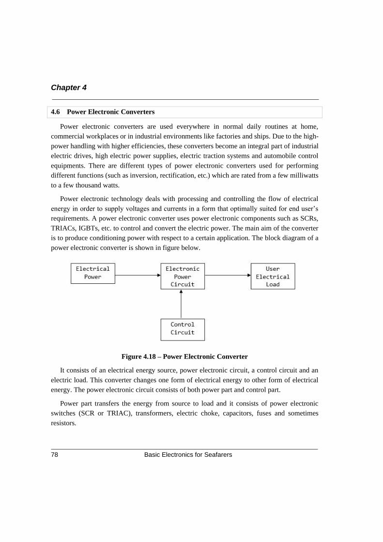
Chapter 4
Basic Electronics for Seafarers 78
4.6 Power Electronic Converters
Power electronic converters are used everywhere in normal daily routines at home,
commercial workplaces or in industrial environments like factories and ships. Due to the high-
power handling with higher efficiencies, these converters become an integral part of industrial
electric drives, high electric power supplies, electric traction systems and automobile control
equipments. There are different types of power electronic converters used for performing
different functions (such as inversion, rectification, etc.) which are rated from a few milliwatts
to a few thousand watts.
Power electronic technology deals with processing and controlling the flow of electrical
energy in order to supply voltages and currents in a form that optimally suited for end user’s
requirements. A power electronic converter uses power electronic components such as SCRs,
TRIACs, IGBTs, etc. to control and convert the electric power. The main aim of the converter
is to produce conditioning power with respect to a certain application. The block diagram of a
power electronic converter is shown in figure below.
Figure 4.18 – Power Electronic Converter
It consists of an electrical energy source, power electronic circuit, a control circuit and an
electric load. This converter changes one form of electrical energy to other form of electrical
energy. The power electronic circuit consists of both power part and control part.
Power part transfers the energy from source to load and it consists of power electronic
switches (SCR or TRIAC), transformers, electric choke, capacitors, fuses and sometimes
resistors.
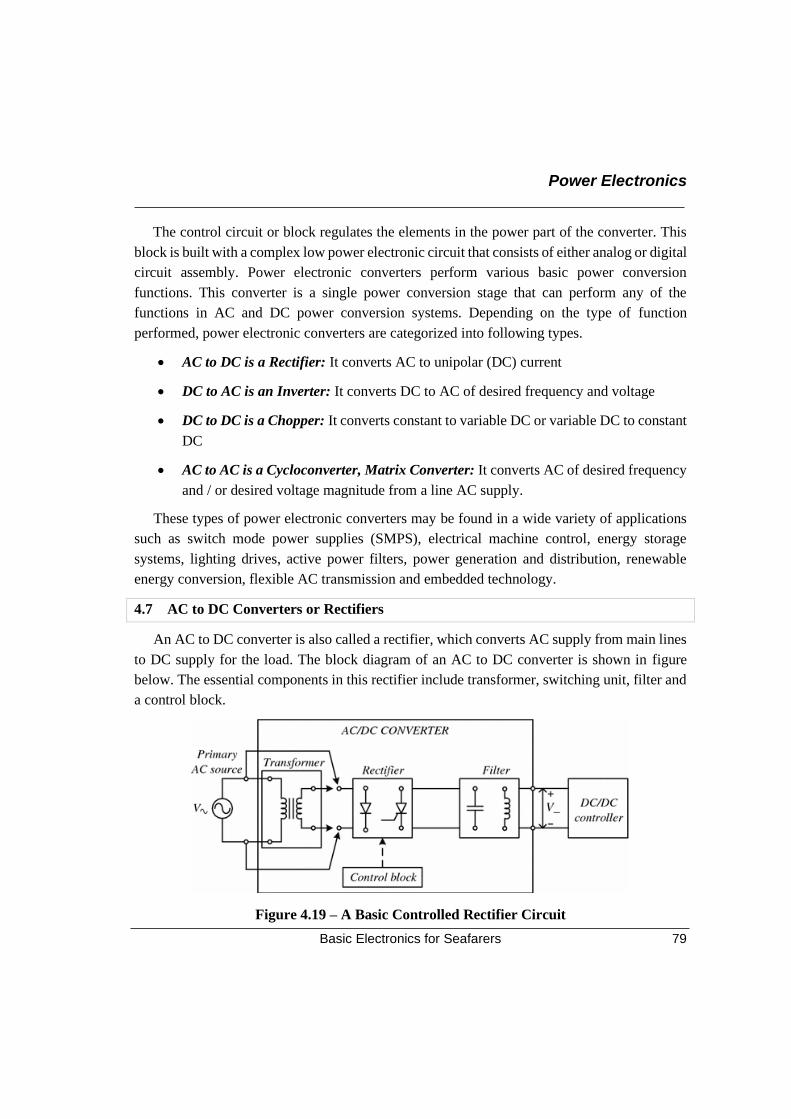
Power Electronics
Basic Electronics for Seafarers 79
The control circuit or block regulates the elements in the power part of the converter. This
block is built with a complex low power electronic circuit that consists of either analog or digital
circuit assembly. Power electronic converters perform various basic power conversion
functions. This converter is a single power conversion stage that can perform any of the
functions in AC and DC power conversion systems. Depending on the type of function
performed, power electronic converters are categorized into following types.
• AC to DC is a Rectifier: It converts AC to unipolar (DC) current
• DC to AC is an Inverter: It converts DC to AC of desired frequency and voltage
• DC to DC is a Chopper: It converts constant to variable DC or variable DC to constant
DC
• AC to AC is a Cycloconverter, Matrix Converter: It converts AC of desired frequency
and / or desired voltage magnitude from a line AC supply.
These types of power electronic converters may be found in a wide variety of applications
such as switch mode power supplies (SMPS), electrical machine control, energy storage
systems, lighting drives, active power filters, power generation and distribution, renewable
energy conversion, flexible AC transmission and embedded technology.
4.7 AC to DC Converters or Rectifiers
An AC to DC converter is also called a rectifier, which converts AC supply from main lines
to DC supply for the load. The block diagram of an AC to DC converter is shown in figure
below. The essential components in this rectifier include transformer, switching unit, filter and
a control block.
Figure 4.19 – A Basic Controlled Rectifier Circuit
Chapter 4
Basic Electronics for Seafarers 80
Here, the transformer adjusts the primary AC source supply to the input of rectifier stage.
Usually, it is a step-down transformer that reduces the supply voltage to a circuit operating
range. The rectifier converts the low voltage AC supply into DC supply. It comprises diode
and/or thyristors based on type of rectifier. The output of the rectifier is of pulsed DC and hence
it is filtered using filter circuit, which is usually made with a capacitor or a choke. The control
block controls the firing angle of thyristors in case of phase-controlled rectifiers. Since the diode
is not a controllable device, control block is not needed in case of diode rectifiers.
Rectifiers are majorly classified into two types
a) Uncontrolled diode rectifiers
b) Controlled rectifiers
a) Uncontrolled Diode Rectifiers
This type of rectifier converts AC voltage from mains into a fixed DC voltage. Since the diodes
are uncontrollable components (which do not require any triggering), these converters are called
as uncontrolled converters as they produce a fixed voltage. The input voltage can be either
single phase or three-phase.
The diode rectifiers are classified into following types.
1. Single phase half-wave rectifier
2. Single phase center-tapped full-wave rectifier
3. Single phase full-wave bridge rectifier
4. Three-phase Half-wave diode rectifier
5. Three-phase full-wave diode bridge rectifier
1. Single Phase Half-Wave Rectifier
The half wave rectifier is a type of rectifier that rectifies only half cycle of the waveform.
The half rectifier consists of a step-down transformer, a diode connected to the transformer and
a load resistance connected to the cathode end of the diode. The circuit diagram of half wave
transformer is shown in the image.
The main supply voltage is given to the transformer which will increase or decrease the
voltage and give to the diode. In most of the cases we will decrease the supply voltage by using
the step-down transformer here also the output of the step-down transformer will be in AC.
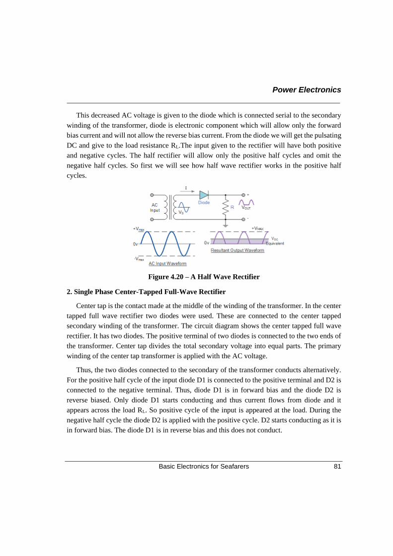
Power Electronics
Basic Electronics for Seafarers 81
This decreased AC voltage is given to the diode which is connected serial to the secondary
winding of the transformer, diode is electronic component which will allow only the forward
bias current and will not allow the reverse bias current. From the diode we will get the pulsating
DC and give to the load resistance RL.The input given to the rectifier will have both positive
and negative cycles. The half rectifier will allow only the positive half cycles and omit the
negative half cycles. So first we will see how half wave rectifier works in the positive half
cycles.
Figure 4.20 – A Half Wave Rectifier
2. Single Phase Center-Tapped Full-Wave Rectifier
Center tap is the contact made at the middle of the winding of the transformer. In the center
tapped full wave rectifier two diodes were used. These are connected to the center tapped
secondary winding of the transformer. The circuit diagram shows the center tapped full wave
rectifier. It has two diodes. The positive terminal of two diodes is connected to the two ends of
the transformer. Center tap divides the total secondary voltage into equal parts. The primary
winding of the center tap transformer is applied with the AC voltage.
Thus, the two diodes connected to the secondary of the transformer conducts alternatively.
For the positive half cycle of the input diode D1 is connected to the positive terminal and D2 is
connected to the negative terminal. Thus, diode D1 is in forward bias and the diode D2 is
reverse biased. Only diode D1 starts conducting and thus current flows from diode and it
appears across the load RL. So positive cycle of the input is appeared at the load. During the
negative half cycle the diode D2 is applied with the positive cycle. D2 starts conducting as it is
in forward bias. The diode D1 is in reverse bias and this does not conduct.
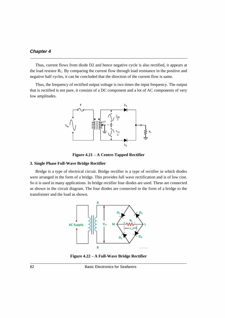
Chapter 4
Basic Electronics for Seafarers 82
Thus, current flows from diode D2 and hence negative cycle is also rectified, it appears at
the load resistor RL. By comparing the current flow through load resistance in the positive and
negative half cycles, it can be concluded that the direction of the current flow is same.
Thus, the frequency of rectified output voltage is two times the input frequency. The output
that is rectified is not pure, it consists of a DC component and a lot of AC components of very
low amplitudes.
Figure 4.21 – A Centre-Tapped Rectifier
3. Single Phase Full-Wave Bridge Rectifier
Bridge is a type of electrical circuit. Bridge rectifier is a type of rectifier in which diodes
were arranged in the form of a bridge. This provides full wave rectification and is of low cost.
So it is used in many applications. In bridge rectifier four diodes are used. These are connected
as shown in the circuit diagram. The four diodes are connected in the form of a bridge to the
transformer and the load as shown.
Figure 4.22 – A Full-Wave Bridge Rectifier
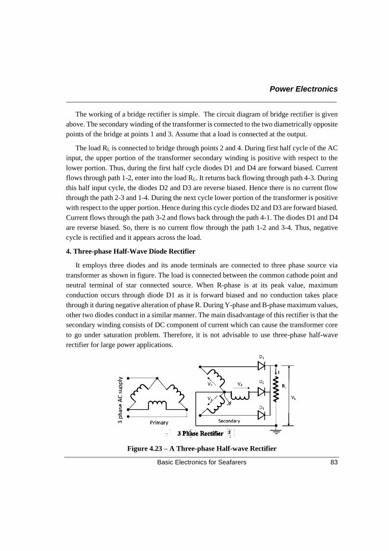
Power Electronics
Basic Electronics for Seafarers 83
The working of a bridge rectifier is simple. The circuit diagram of bridge rectifier is given
above. The secondary winding of the transformer is connected to the two diametrically opposite
points of the bridge at points 1 and 3. Assume that a load is connected at the output.
The load RL is connected to bridge through points 2 and 4. During first half cycle of the AC
input, the upper portion of the transformer secondary winding is positive with respect to the
lower portion. Thus, during the first half cycle diodes D1 and D4 are forward biased. Current
flows through path 1-2, enter into the load RL. It returns back flowing through path 4-3. During
this half input cycle, the diodes D2 and D3 are reverse biased. Hence there is no current flow
through the path 2-3 and 1-4. During the next cycle lower portion of the transformer is positive
with respect to the upper portion. Hence during this cycle diodes D2 and D3 are forward biased.
Current flows through the path 3-2 and flows back through the path 4-1. The diodes D1 and D4
are reverse biased. So, there is no current flow through the path 1-2 and 3-4. Thus, negative
cycle is rectified and it appears across the load.
4. Three-phase Half-Wave Diode Rectifier
It employs three diodes and its anode terminals are connected to three phase source via
transformer as shown in figure. The load is connected between the common cathode point and
neutral terminal of star connected source. When R-phase is at its peak value, maximum
conduction occurs through diode D1 as it is forward biased and no conduction takes place
through it during negative alteration of phase R. During Y-phase and B-phase maximum values,
other two diodes conduct in a similar manner. The main disadvantage of this rectifier is that the
secondary winding consists of DC component of current which can cause the transformer core
to go under saturation problem. Therefore, it is not advisable to use three-phase half-wave
rectifier for large power applications.
Figure 4.23 – A Three-phase Half-wave Rectifier
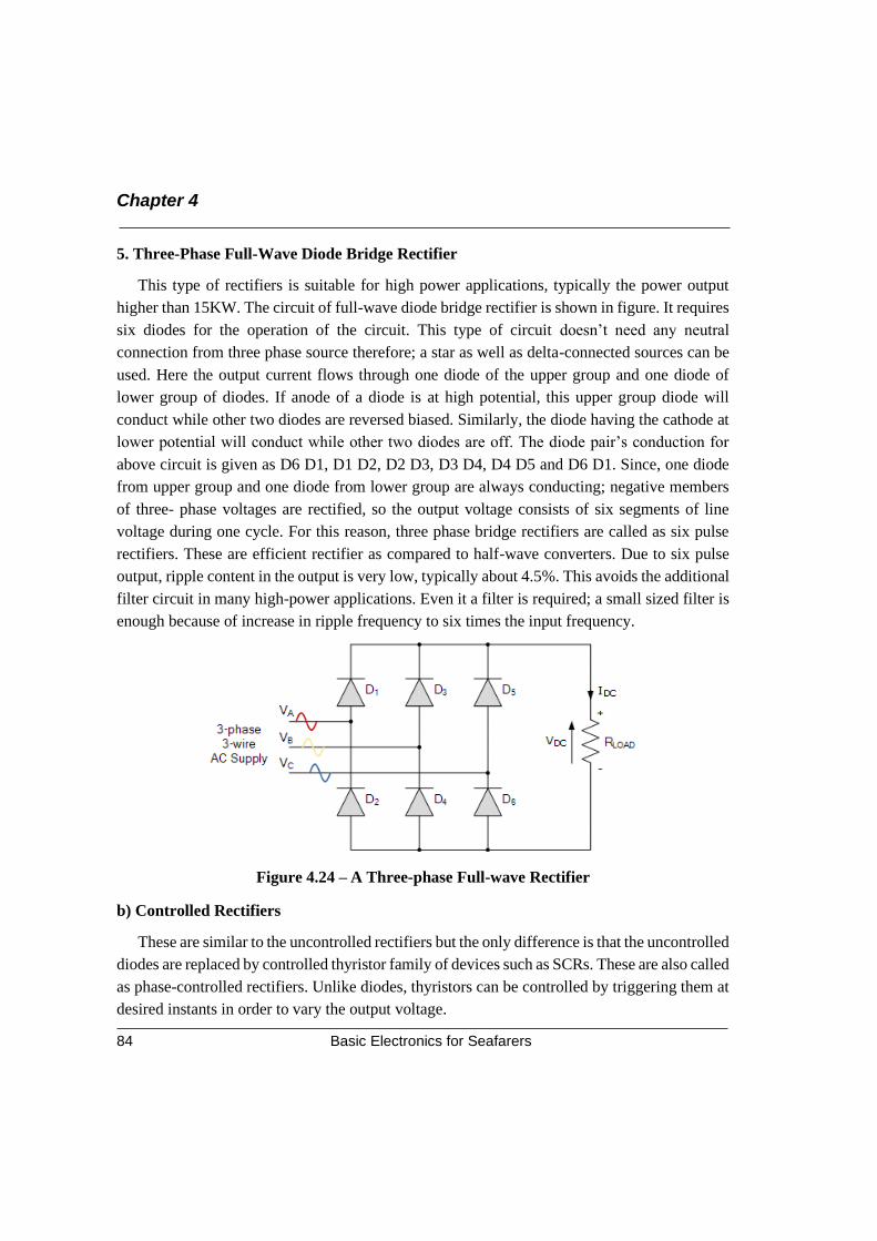
Chapter 4
Basic Electronics for Seafarers 84
5. Three-Phase Full-Wave Diode Bridge Rectifier
This type of rectifiers is suitable for high power applications, typically the power output
higher than 15KW. The circuit of full-wave diode bridge rectifier is shown in figure. It requires
six diodes for the operation of the circuit. This type of circuit doesn’t need any neutral
connection from three phase source therefore; a star as well as delta-connected sources can be
used. Here the output current flows through one diode of the upper group and one diode of
lower group of diodes. If anode of a diode is at high potential, this upper group diode will
conduct while other two diodes are reversed biased. Similarly, the diode having the cathode at
lower potential will conduct while other two diodes are off. The diode pair’s conduction for
above circuit is given as D6 D1, D1 D2, D2 D3, D3 D4, D4 D5 and D6 D1. Since, one diode
from upper group and one diode from lower group are always conducting; negative members
of three- phase voltages are rectified, so the output voltage consists of six segments of line
voltage during one cycle. For this reason, three phase bridge rectifiers are called as six pulse
rectifiers. These are efficient rectifier as compared to half-wave converters. Due to six pulse
output, ripple content in the output is very low, typically about 4.5%. This avoids the additional
filter circuit in many high-power applications. Even it a filter is required; a small sized filter is
enough because of increase in ripple frequency to six times the input frequency.
Figure 4.24 – A Three-phase Full-wave Rectifier
b) Controlled Rectifiers
These are similar to the uncontrolled rectifiers but the only difference is that the uncontrolled
diodes are replaced by controlled thyristor family of devices such as SCRs. These are also called
as phase-controlled rectifiers. Unlike diodes, thyristors can be controlled by triggering them at
desired instants in order to vary the output voltage.
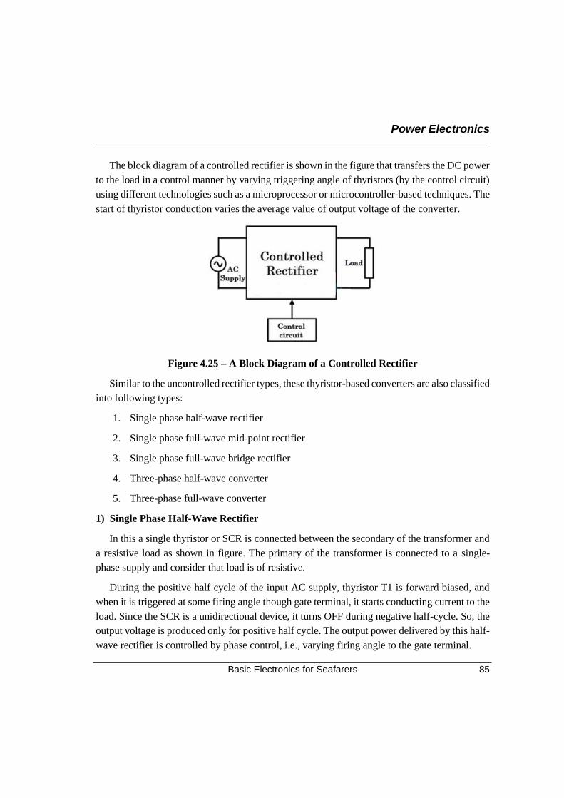
Power Electronics
Basic Electronics for Seafarers 85
The block diagram of a controlled rectifier is shown in the figure that transfers the DC power
to the load in a control manner by varying triggering angle of thyristors (by the control circuit)
using different technologies such as a microprocessor or microcontroller-based techniques. The
start of thyristor conduction varies the average value of output voltage of the converter.
Figure 4.25 – A Block Diagram of a Controlled Rectifier
Similar to the uncontrolled rectifier types, these thyristor-based converters are also classified
into following types:
1. Single phase half-wave rectifier
2. Single phase full-wave mid-point rectifier
3. Single phase full-wave bridge rectifier
4. Three-phase half-wave converter
5. Three-phase full-wave converter
1) Single Phase Half-Wave Rectifier
In this a single thyristor or SCR is connected between the secondary of the transformer and
a resistive load as shown in figure. The primary of the transformer is connected to a single-
phase supply and consider that load is of resistive.
During the positive half cycle of the input AC supply, thyristor T1 is forward biased, and
when it is triggered at some firing angle though gate terminal, it starts conducting current to the
load. Since the SCR is a unidirectional device, it turns OFF during negative half-cycle. So, the
output voltage is produced only for positive half cycle. The output power delivered by this half-
wave rectifier is controlled by phase control, i.e., varying firing angle to the gate terminal.
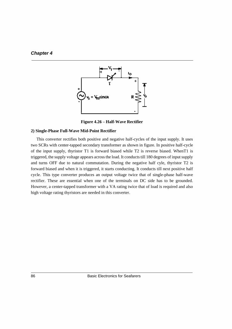
Chapter 4
Basic Electronics for Seafarers 86
Figure 4.26 – Half-Wave Rectifier
2) Single-Phase Full-Wave Mid-Point Rectifier
This converter rectifies both positive and negative half-cycles of the input supply. It uses
two SCRs with center-tapped secondary transformer as shown in figure. In positive half-cycle
of the input supply, thyristor T1 is forward biased while T2 is reverse biased. WhenT1 is
triggered, the supply voltage appears across the load. It conducts till 180 degrees of input supply
and turns OFF due to natural commutation. During the negative half cyle, thyristor T2 is
forward biased and when it is triggered, it starts conducting. It conducts till next positive half
cycle. This type converter produces an output voltage twice that of single-phase half-wave
rectifier. These are essential when one of the terminals on DC side has to be grounded.
However, a center-tapped transformer with a VA rating twice that of load is required and also
high voltage rating thyristors are needed in this converter.
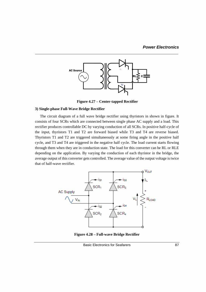
Power Electronics
Basic Electronics for Seafarers 87
Figure 4.27 – Center-tapped Rectifier
3) Single-phase Full-Wave Bridge Rectifier
The circuit diagram of a full wave bridge rectifier using thyristors in shown in figure. It
consists of four SCRs which are connected between single phase AC supply and a load. This
rectifier produces controllable DC by varying conduction of all SCRs. In positive half-cycle of
the input, thyristors T1 and T2 are forward biased while T3 and T4 are reverse biased.
Thyristors T1 and T2 are triggered simultaneously at some firing angle in the positive half
cycle, and T3 and T4 are triggered in the negative half cycle. The load current starts flowing
through them when they are in conduction state. The load for this converter can be RL or RLE
depending on the application. By varying the conduction of each thyristor in the bridge, the
average output of this converter gets controlled. The average value of the output voltage is twice
that of half-wave rectifier.
Figure 4.28 – Full-wave Bridge Rectifier
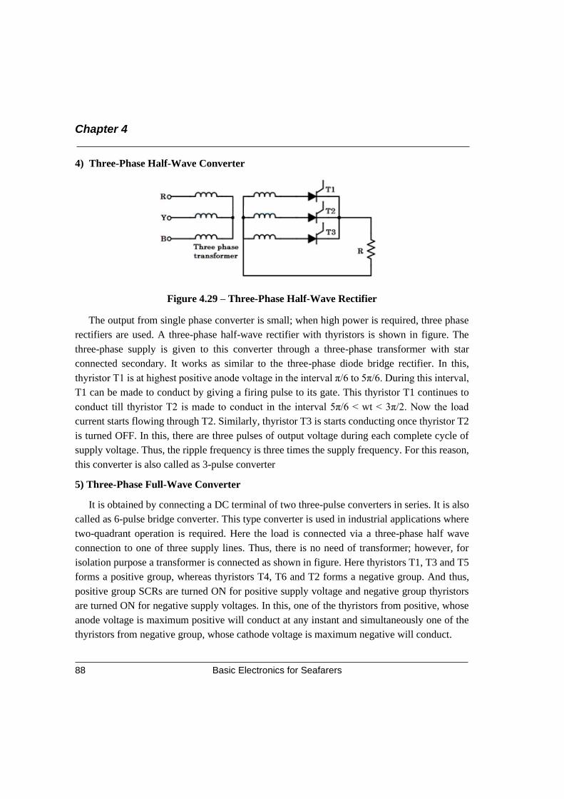
Chapter 4
Basic Electronics for Seafarers 88
4) Three-Phase Half-Wave Converter
Figure 4.29 – Three-Phase Half-Wave Rectifier
The output from single phase converter is small; when high power is required, three phase
rectifiers are used. A three-phase half-wave rectifier with thyristors is shown in figure. The
three-phase supply is given to this converter through a three-phase transformer with star
connected secondary. It works as similar to the three-phase diode bridge rectifier. In this,
thyristor T1 is at highest positive anode voltage in the interval π/6 to 5π/6. During this interval,
T1 can be made to conduct by giving a firing pulse to its gate. This thyristor T1 continues to
conduct till thyristor T2 is made to conduct in the interval 5π/6 < wt < 3π/2. Now the load
current starts flowing through T2. Similarly, thyristor T3 is starts conducting once thyristor T2
is turned OFF. In this, there are three pulses of output voltage during each complete cycle of
supply voltage. Thus, the ripple frequency is three times the supply frequency. For this reason,
this converter is also called as 3-pulse converter
5) Three-Phase Full-Wave Converter
It is obtained by connecting a DC terminal of two three-pulse converters in series. It is also
called as 6-pulse bridge converter. This type converter is used in industrial applications where
two-quadrant operation is required. Here the load is connected via a three-phase half wave
connection to one of three supply lines. Thus, there is no need of transformer; however, for
isolation purpose a transformer is connected as shown in figure. Here thyristors T1, T3 and T5
forms a positive group, whereas thyristors T4, T6 and T2 forms a negative group. And thus,
positive group SCRs are turned ON for positive supply voltage and negative group thyristors
are turned ON for negative supply voltages. In this, one of the thyristors from positive, whose
anode voltage is maximum positive will conduct at any instant and simultaneously one of the
thyristors from negative group, whose cathode voltage is maximum negative will conduct.
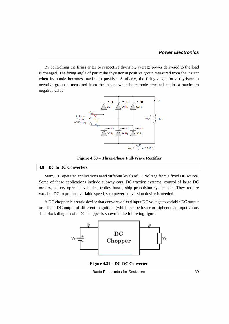
Power Electronics
Basic Electronics for Seafarers 89
By controlling the firing angle to respective thyristor, average power delivered to the load
is changed. The firing angle of particular thyristor in positive group measured from the instant
when its anode becomes maximum positive. Similarly, the firing angle for a thyristor in
negative group is measured from the instant when its cathode terminal attains a maximum
negative value.
Figure 4.30 – Three-Phase Full-Wave Rectifier
4.8 DC to DC Converters
Many DC operated applications need different levels of DC voltage from a fixed DC source.
Some of these applications include subway cars, DC traction systems, control of large DC
motors, battery operated vehicles, trolley buses, ship propulsion system, etc. They require
variable DC to produce variable speed, so a power conversion device is needed.
A DC chopper is a static device that converts a fixed input DC voltage to variable DC output
or a fixed DC output of different magnitude (which can be lower or higher) than input value.
The block diagram of a DC chopper is shown in the following figure.
Figure 4.31 – DC-DC Converter
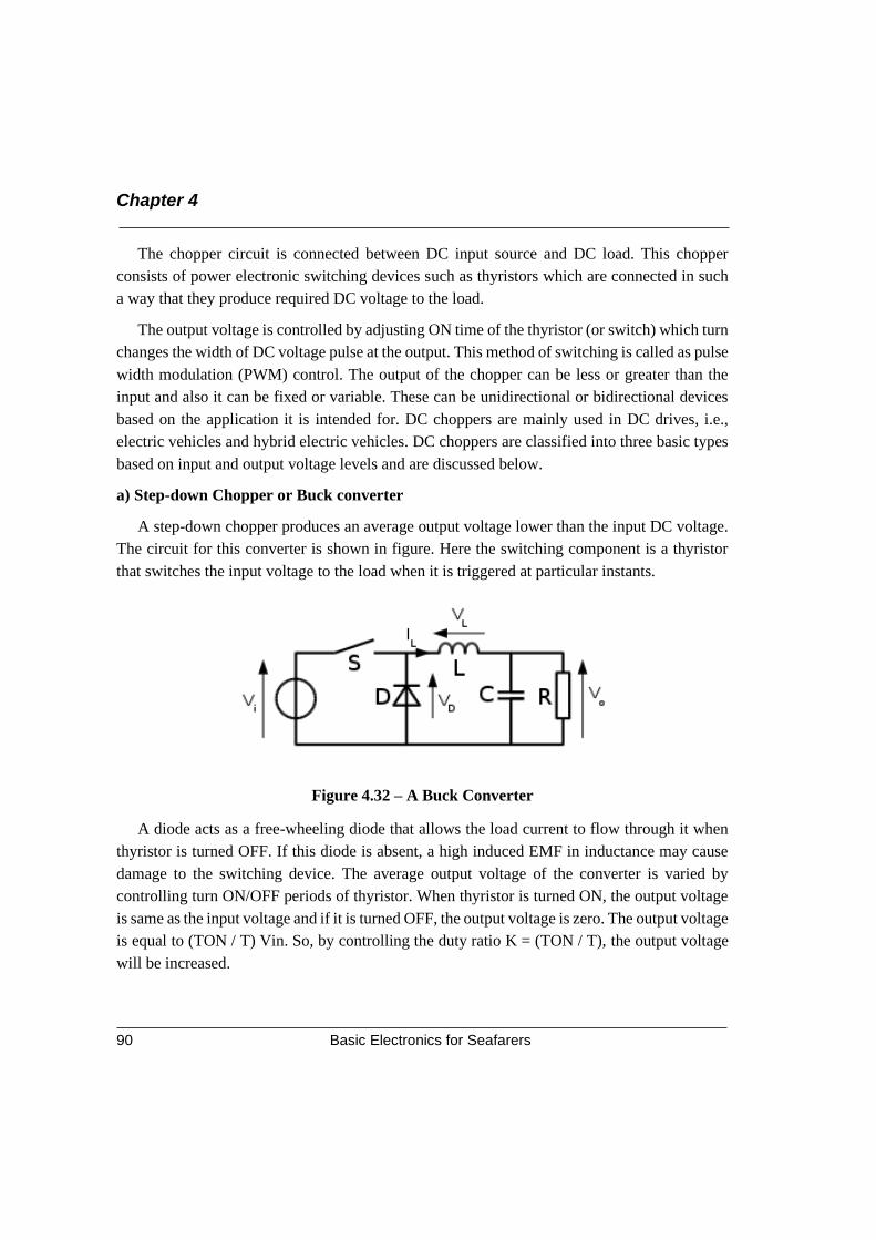
Chapter 4
Basic Electronics for Seafarers 90
The chopper circuit is connected between DC input source and DC load. This chopper
consists of power electronic switching devices such as thyristors which are connected in such
a way that they produce required DC voltage to the load.
The output voltage is controlled by adjusting ON time of the thyristor (or switch) which turn
changes the width of DC voltage pulse at the output. This method of switching is called as pulse
width modulation (PWM) control. The output of the chopper can be less or greater than the
input and also it can be fixed or variable. These can be unidirectional or bidirectional devices
based on the application it is intended for. DC choppers are mainly used in DC drives, i.e.,
electric vehicles and hybrid electric vehicles. DC choppers are classified into three basic types
based on input and output voltage levels and are discussed below.
a) Step-down Chopper or Buck converter
A step-down chopper produces an average output voltage lower than the input DC voltage.
The circuit for this converter is shown in figure. Here the switching component is a thyristor
that switches the input voltage to the load when it is triggered at particular instants.
Figure 4.32 – A Buck Converter
A diode acts as a free-wheeling diode that allows the load current to flow through it when
thyristor is turned OFF. If this diode is absent, a high induced EMF in inductance may cause
damage to the switching device. The average output voltage of the converter is varied by
controlling turn ON/OFF periods of thyristor. When thyristor is turned ON, the output voltage
is same as the input voltage and if it is turned OFF, the output voltage is zero. The output voltage
is equal to (TON / T) Vin. So, by controlling the duty ratio K = (TON / T), the output voltage
will be increased.
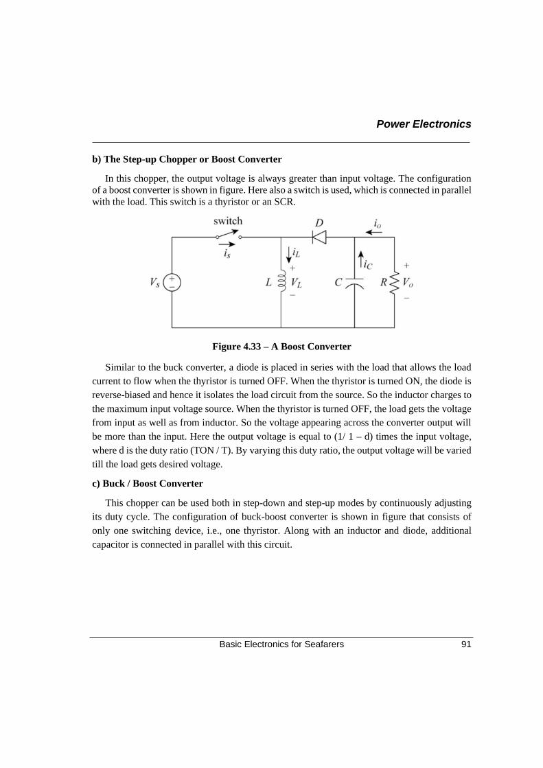
Power Electronics
Basic Electronics for Seafarers 91
b) The Step-up Chopper or Boost Converter
In this chopper, the output voltage is always greater than input voltage. The configuration
of a boost converter is shown in figure. Here also a switch is used, which is connected in parallel
with the load. This switch is a thyristor or an SCR.
Figure 4.33 – A Boost Converter
Similar to the buck converter, a diode is placed in series with the load that allows the load
current to flow when the thyristor is turned OFF. When the thyristor is turned ON, the diode is
reverse-biased and hence it isolates the load circuit from the source. So the inductor charges to
the maximum input voltage source. When the thyristor is turned OFF, the load gets the voltage
from input as well as from inductor. So the voltage appearing across the converter output will
be more than the input. Here the output voltage is equal to (1/ 1 – d) times the input voltage,
where d is the duty ratio (TON / T). By varying this duty ratio, the output voltage will be varied
till the load gets desired voltage.
c) Buck / Boost Converter
This chopper can be used both in step-down and step-up modes by continuously adjusting
its duty cycle. The configuration of buck-boost converter is shown in figure that consists of
only one switching device, i.e., one thyristor. Along with an inductor and diode, additional
capacitor is connected in parallel with this circuit.
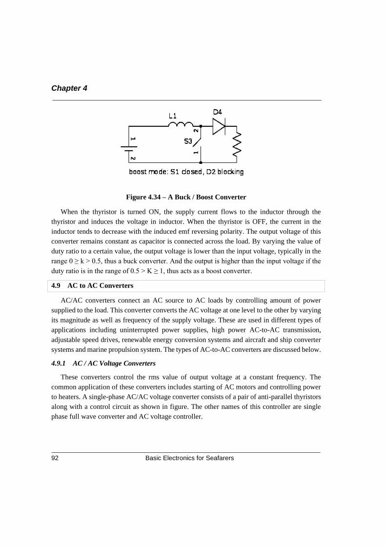
Chapter 4
Basic Electronics for Seafarers 92
Figure 4.34 – A Buck / Boost Converter
When the thyristor is turned ON, the supply current flows to the inductor through the
thyristor and induces the voltage in inductor. When the thyristor is OFF, the current in the
inductor tends to decrease with the induced emf reversing polarity. The output voltage of this
converter remains constant as capacitor is connected across the load. By varying the value of
duty ratio to a certain value, the output voltage is lower than the input voltage, typically in the
range 0 ≥ k > 0.5, thus a buck converter. And the output is higher than the input voltage if the
duty ratio is in the range of 0.5 > K ≥ 1, thus acts as a boost converter.
4.9 AC to AC Converters
AC/AC converters connect an AC source to AC loads by controlling amount of power
supplied to the load. This converter converts the AC voltage at one level to the other by varying
its magnitude as well as frequency of the supply voltage. These are used in different types of
applications including uninterrupted power supplies, high power AC-to-AC transmission,
adjustable speed drives, renewable energy conversion systems and aircraft and ship converter
systems and marine propulsion system. The types of AC-to-AC converters are discussed below.
4.9.1 AC / AC Voltage Converters
These converters control the rms value of output voltage at a constant frequency. The
common application of these converters includes starting of AC motors and controlling power
to heaters. A single-phase AC/AC voltage converter consists of a pair of anti-parallel thyristors
along with a control circuit as shown in figure. The other names of this controller are single
phase full wave converter and AC voltage controller.
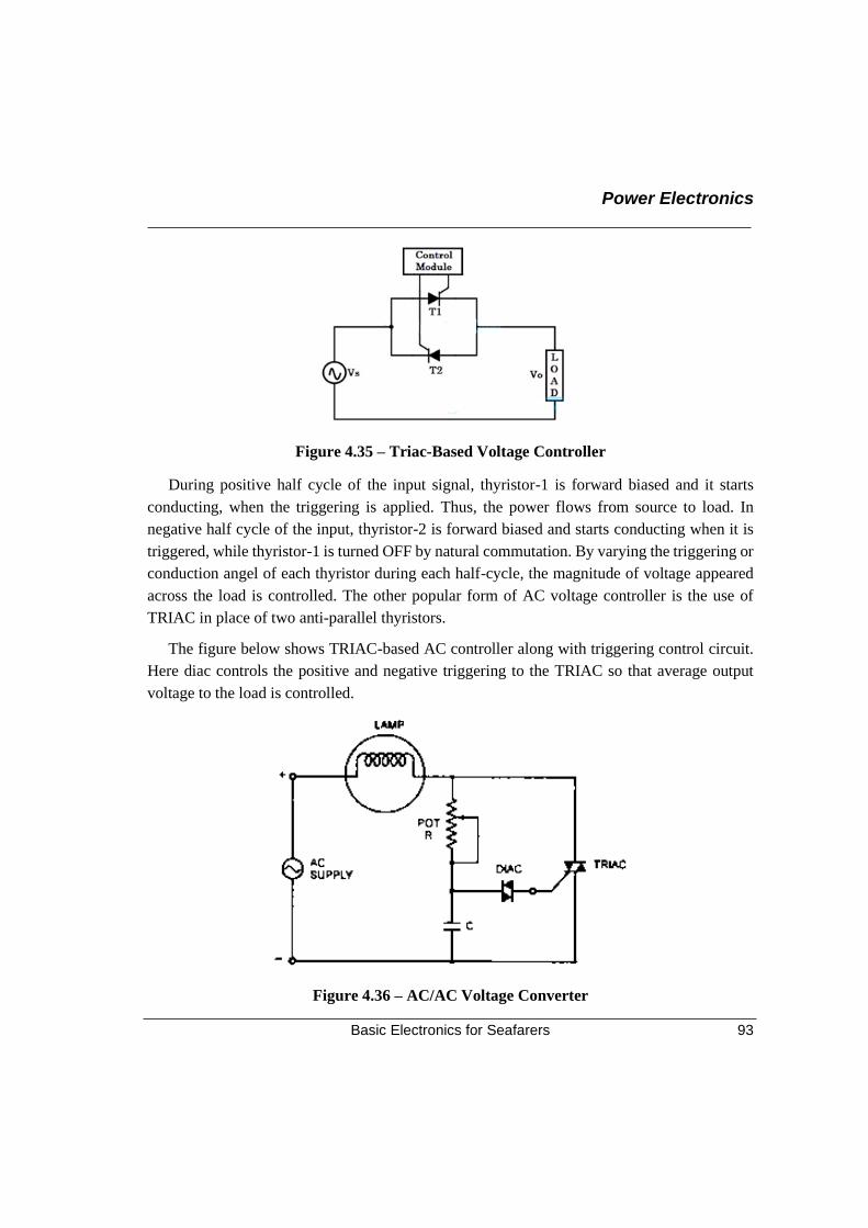
Power Electronics
Basic Electronics for Seafarers 93
Figure 4.35 – Triac-Based Voltage Controller
During positive half cycle of the input signal, thyristor-1 is forward biased and it starts
conducting, when the triggering is applied. Thus, the power flows from source to load. In
negative half cycle of the input, thyristor-2 is forward biased and starts conducting when it is
triggered, while thyristor-1 is turned OFF by natural commutation. By varying the triggering or
conduction angel of each thyristor during each half-cycle, the magnitude of voltage appeared
across the load is controlled. The other popular form of AC voltage controller is the use of
TRIAC in place of two anti-parallel thyristors.
The figure below shows TRIAC-based AC controller along with triggering control circuit.
Here diac controls the positive and negative triggering to the TRIAC so that average output
voltage to the load is controlled.
Figure 4.36 – AC/AC Voltage Converter
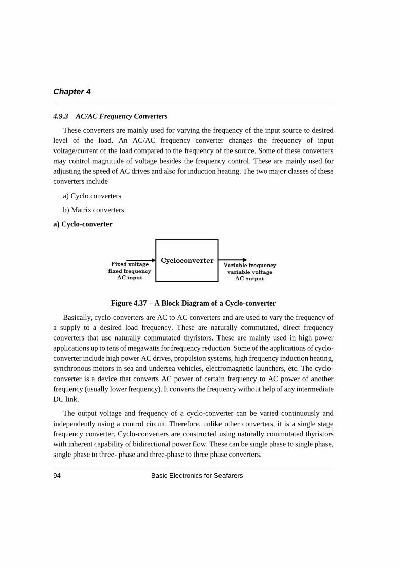
Chapter 4
Basic Electronics for Seafarers 94
4.9.3 AC/AC Frequency Converters
These converters are mainly used for varying the frequency of the input source to desired
level of the load. An AC/AC frequency converter changes the frequency of input
voltage/current of the load compared to the frequency of the source. Some of these converters
may control magnitude of voltage besides the frequency control. These are mainly used for
adjusting the speed of AC drives and also for induction heating. The two major classes of these
converters include
a) Cyclo converters
b) Matrix converters.
a) Cyclo-converter
Figure 4.37 – A Block Diagram of a Cyclo-converter
Basically, cyclo-converters are AC to AC converters and are used to vary the frequency of
a supply to a desired load frequency. These are naturally commutated, direct frequency
converters that use naturally commutated thyristors. These are mainly used in high power
applications up to tens of megawatts for frequency reduction. Some of the applications of cyclo-
converter include high power AC drives, propulsion systems, high frequency induction heating,
synchronous motors in sea and undersea vehicles, electromagnetic launchers, etc. The cyclo-
converter is a device that converts AC power of certain frequency to AC power of another
frequency (usually lower frequency). It converts the frequency without help of any intermediate
DC link.
The output voltage and frequency of a cyclo-converter can be varied continuously and
independently using a control circuit. Therefore, unlike other converters, it is a single stage
frequency converter. Cyclo-converters are constructed using naturally commutated thyristors
with inherent capability of bidirectional power flow. These can be single phase to single phase,
single phase to three- phase and three-phase to three phase converters.
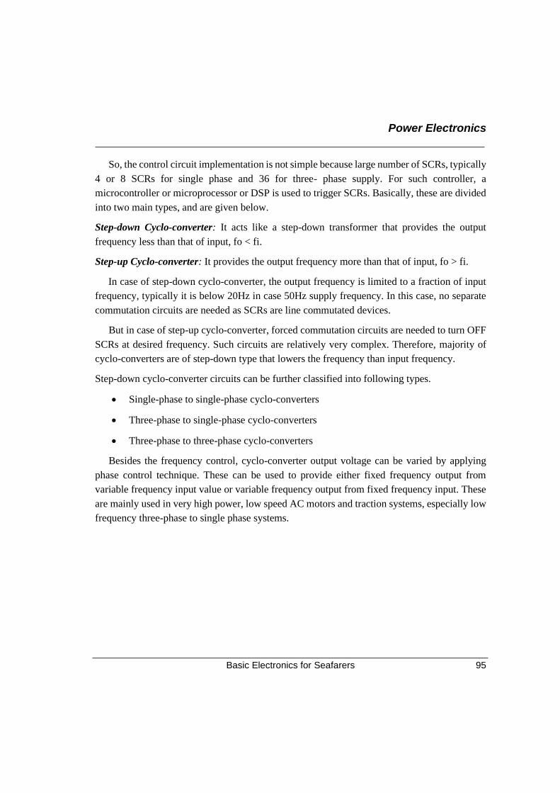
Power Electronics
Basic Electronics for Seafarers 95
So, the control circuit implementation is not simple because large number of SCRs, typically
4 or 8 SCRs for single phase and 36 for three- phase supply. For such controller, a
microcontroller or microprocessor or DSP is used to trigger SCRs. Basically, these are divided
into two main types, and are given below.
Step-down Cyclo-converter: It acts like a step-down transformer that provides the output
frequency less than that of input, fo < fi.
Step-up Cyclo-converter: It provides the output frequency more than that of input, fo > fi.
In case of step-down cyclo-converter, the output frequency is limited to a fraction of input
frequency, typically it is below 20Hz in case 50Hz supply frequency. In this case, no separate
commutation circuits are needed as SCRs are line commutated devices.
But in case of step-up cyclo-converter, forced commutation circuits are needed to turn OFF
SCRs at desired frequency. Such circuits are relatively very complex. Therefore, majority of
cyclo-converters are of step-down type that lowers the frequency than input frequency.
Step-down cyclo-converter circuits can be further classified into following types.
• Single-phase to single-phase cyclo-converters
• Three-phase to single-phase cyclo-converters
• Three-phase to three-phase cyclo-converters
Besides the frequency control, cyclo-converter output voltage can be varied by applying
phase control technique. These can be used to provide either fixed frequency output from
variable frequency input value or variable frequency output from fixed frequency input. These
are mainly used in very high power, low speed AC motors and traction systems, especially low
frequency three-phase to single phase systems.
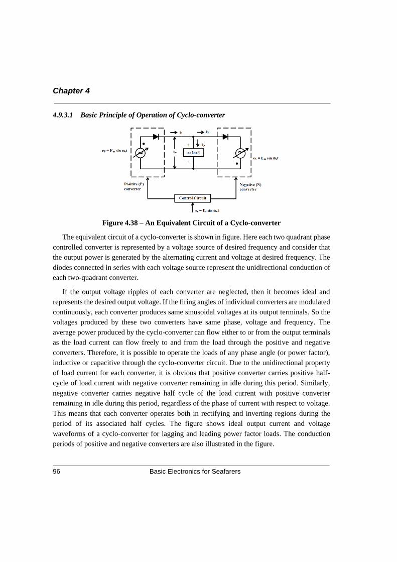
Chapter 4
Basic Electronics for Seafarers 96
4.9.3.1 Basic Principle of Operation of Cyclo-converter
Figure 4.38 – An Equivalent Circuit of a Cyclo-converter
The equivalent circuit of a cyclo-converter is shown in figure. Here each two quadrant phase
controlled converter is represented by a voltage source of desired frequency and consider that
the output power is generated by the alternating current and voltage at desired frequency. The
diodes connected in series with each voltage source represent the unidirectional conduction of
each two-quadrant converter.
If the output voltage ripples of each converter are neglected, then it becomes ideal and
represents the desired output voltage. If the firing angles of individual converters are modulated
continuously, each converter produces same sinusoidal voltages at its output terminals. So the
voltages produced by these two converters have same phase, voltage and frequency. The
average power produced by the cyclo-converter can flow either to or from the output terminals
as the load current can flow freely to and from the load through the positive and negative
converters. Therefore, it is possible to operate the loads of any phase angle (or power factor),
inductive or capacitive through the cyclo-converter circuit. Due to the unidirectional property
of load current for each converter, it is obvious that positive converter carries positive half-
cycle of load current with negative converter remaining in idle during this period. Similarly,
negative converter carries negative half cycle of the load current with positive converter
remaining in idle during this period, regardless of the phase of current with respect to voltage.
This means that each converter operates both in rectifying and inverting regions during the
period of its associated half cycles. The figure shows ideal output current and voltage
waveforms of a cyclo-converter for lagging and leading power factor loads. The conduction
periods of positive and negative converters are also illustrated in the figure.
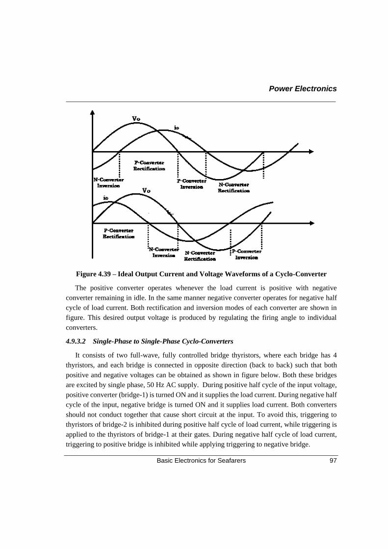
Power Electronics
Basic Electronics for Seafarers 97
Figure 4.39 – Ideal Output Current and Voltage Waveforms of a Cyclo-Converter
The positive converter operates whenever the load current is positive with negative
converter remaining in idle. In the same manner negative converter operates for negative half
cycle of load current. Both rectification and inversion modes of each converter are shown in
figure. This desired output voltage is produced by regulating the firing angle to individual
converters.
4.9.3.2 Single-Phase to Single-Phase Cyclo-Converters
It consists of two full-wave, fully controlled bridge thyristors, where each bridge has 4
thyristors, and each bridge is connected in opposite direction (back to back) such that both
positive and negative voltages can be obtained as shown in figure below. Both these bridges
are excited by single phase, 50 Hz AC supply. During positive half cycle of the input voltage,
positive converter (bridge-1) is turned ON and it supplies the load current. During negative half
cycle of the input, negative bridge is turned ON and it supplies load current. Both converters
should not conduct together that cause short circuit at the input. To avoid this, triggering to
thyristors of bridge-2 is inhibited during positive half cycle of load current, while triggering is
applied to the thyristors of bridge-1 at their gates. During negative half cycle of load current,
triggering to positive bridge is inhibited while applying triggering to negative bridge.
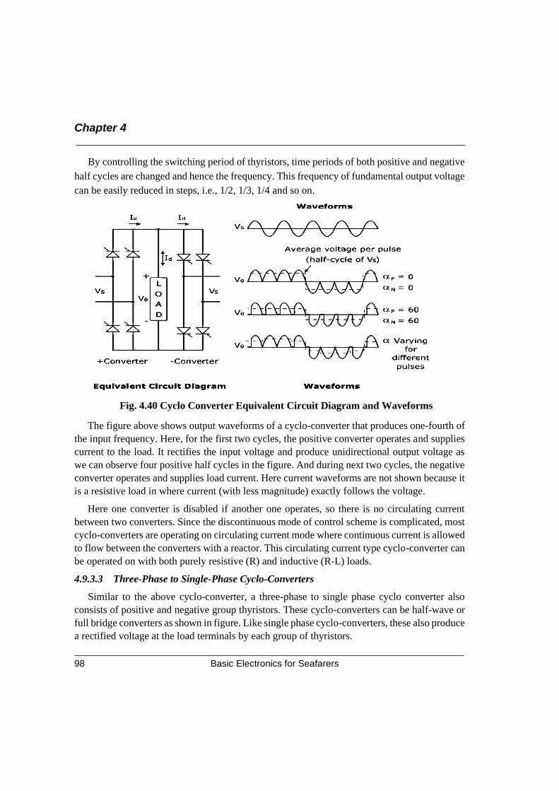
Chapter 4
Basic Electronics for Seafarers 98
By controlling the switching period of thyristors, time periods of both positive and negative
half cycles are changed and hence the frequency. This frequency of fundamental output voltage
can be easily reduced in steps, i.e., 1/2, 1/3, 1/4 and so on.
Fig. 4.40 Cyclo Converter Equivalent Circuit Diagram and Waveforms
The figure above shows output waveforms of a cyclo-converter that produces one-fourth of
the input frequency. Here, for the first two cycles, the positive converter operates and supplies
current to the load. It rectifies the input voltage and produce unidirectional output voltage as
we can observe four positive half cycles in the figure. And during next two cycles, the negative
converter operates and supplies load current. Here current waveforms are not shown because it
is a resistive load in where current (with less magnitude) exactly follows the voltage.
Here one converter is disabled if another one operates, so there is no circulating current
between two converters. Since the discontinuous mode of control scheme is complicated, most
cyclo-converters are operating on circulating current mode where continuous current is allowed
to flow between the converters with a reactor. This circulating current type cyclo-converter can
be operated on with both purely resistive (R) and inductive (R-L) loads.
4.9.3.3 Three-Phase to Single-Phase Cyclo-Converters
Similar to the above cyclo-converter, a three-phase to single phase cyclo converter also
consists of positive and negative group thyristors. These cyclo-converters can be half-wave or
full bridge converters as shown in figure. Like single phase cyclo-converters, these also produce
a rectified voltage at the load terminals by each group of thyristors.
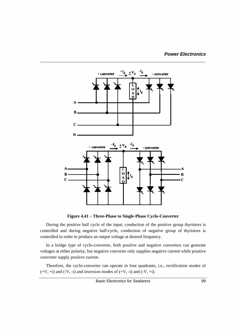
Power Electronics
Basic Electronics for Seafarers 99
Figure 4.41 – Three-Phase to Single-Phase Cyclo-Converter
During the positive half cycle of the input, conduction of the positive group thyristors is
controlled and during negative half-cycle, conduction of negative group of thyristors is
controlled in order to produce an output voltage at desired frequency.
In a bridge type of cyclo-converter, both positive and negative converters can generate
voltages at either polarity, but negative converter only supplies negative current while positive
converter supply positive current.
Therefore, the cyclo-converter can operate in four quadrants, i.e., rectification modes of
(+V, +i) and (-V, -i) and inversion modes of (+V, -i) and (-V, +i).
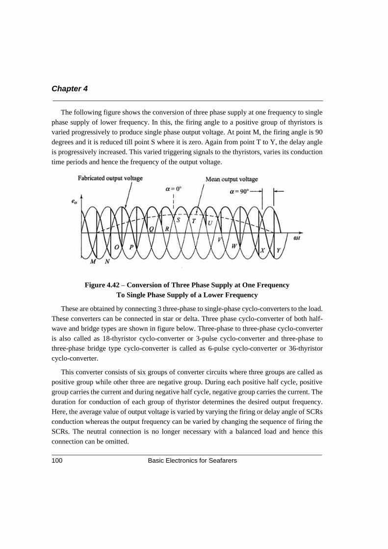
Chapter 4
Basic Electronics for Seafarers 100
The following figure shows the conversion of three phase supply at one frequency to single
phase supply of lower frequency. In this, the firing angle to a positive group of thyristors is
varied progressively to produce single phase output voltage. At point M, the firing angle is 90
degrees and it is reduced till point S where it is zero. Again from point T to Y, the delay angle
is progressively increased. This varied triggering signals to the thyristors, varies its conduction
time periods and hence the frequency of the output voltage.
Figure 4.42 – Conversion of Three Phase Supply at One Frequency
To Single Phase Supply of a Lower Frequency
These are obtained by connecting 3 three-phase to single-phase cyclo-converters to the load.
These converters can be connected in star or delta. Three phase cyclo-converter of both half-
wave and bridge types are shown in figure below. Three-phase to three-phase cyclo-converter
is also called as 18-thyristor cyclo-converter or 3-pulse cyclo-converter and three-phase to
three-phase bridge type cyclo-converter is called as 6-pulse cyclo-converter or 36-thyristor
cyclo-converter.
This converter consists of six groups of converter circuits where three groups are called as
positive group while other three are negative group. During each positive half cycle, positive
group carries the current and during negative half cycle, negative group carries the current. The
duration for conduction of each group of thyristor determines the desired output frequency.
Here, the average value of output voltage is varied by varying the firing or delay angle of SCRs
conduction whereas the output frequency can be varied by changing the sequence of firing the
SCRs. The neutral connection is no longer necessary with a balanced load and hence this
connection can be omitted.
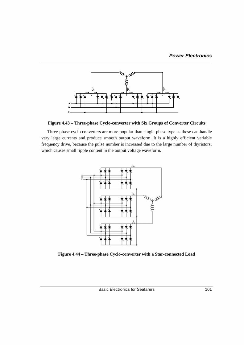
Power Electronics
Basic Electronics for Seafarers 101
Figure 4.43 – Three-phase Cyclo-converter with Six Groups of Converter Circuits
Three-phase cyclo converters are more popular than single-phase type as these can handle
very large currents and produce smooth output waveform. It is a highly efficient variable
frequency drive, because the pulse number is increased due to the large number of thyristors,
which causes small ripple content in the output voltage waveform.
Figure 4.44 – Three-phase Cyclo-converter with a Star-connected Load
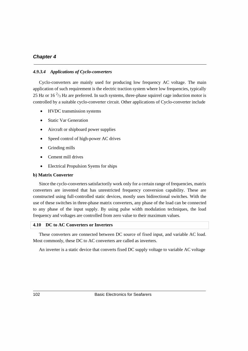
Chapter 4
Basic Electronics for Seafarers 102
4.9.3.4 Applications of Cyclo-converters
Cyclo-converters are mainly used for producing low frequency AC voltage. The main
application of such requirement is the electric traction system where low frequencies, typically
25 Hz or 16 2/3 Hz are preferred. In such systems, three-phase squirrel cage induction motor is
controlled by a suitable cyclo-converter circuit. Other applications of Cyclo-converter include
• HVDC transmission systems
• Static Var Generation
• Aircraft or shipboard power supplies
• Speed control of high-power AC drives
• Grinding mills
• Cement mill drives
• Electrical Propulsion Syems for ships
b) Matrix Converter
Since the cyclo-converters satisfactorily work only for a certain range of frequencies, matrix
converters are invented that has unrestricted frequency conversion capability. These are
constructed using full-controlled static devices, mostly uses bidirectional switches. With the
use of these switches in three-phase matrix converters, any phase of the load can be connected
to any phase of the input supply. By using pulse width modulation techniques, the load
frequency and voltages are controlled from zero value to their maximum values.
4.10 DC to AC Converters or Inverters
These converters are connected between DC source of fixed input, and variable AC load.
Most commonly, these DC to AC converters are called as inverters.
An inverter is a static device that converts fixed DC supply voltage to variable AC voltage
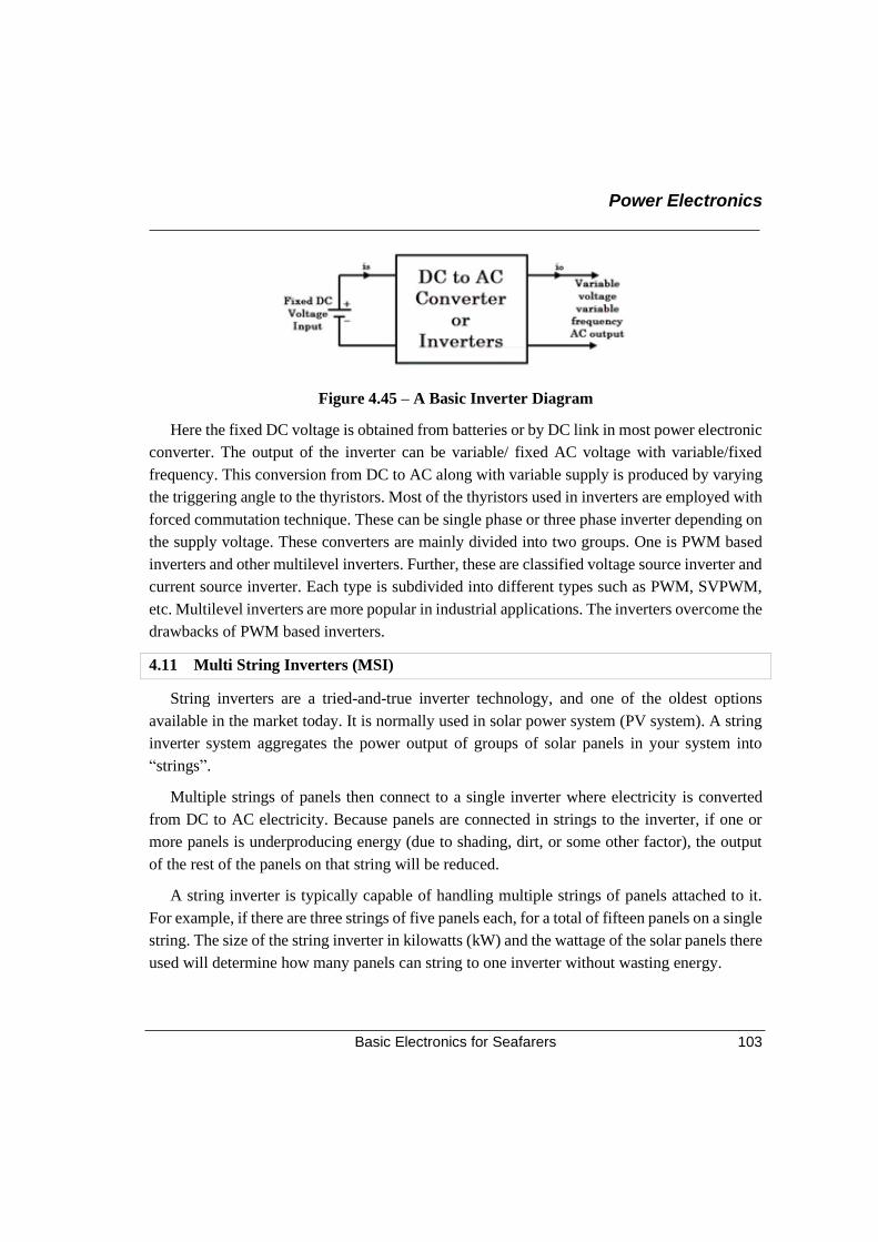
Power Electronics
Basic Electronics for Seafarers 103
Figure 4.45 – A Basic Inverter Diagram
Here the fixed DC voltage is obtained from batteries or by DC link in most power electronic
converter. The output of the inverter can be variable/ fixed AC voltage with variable/fixed
frequency. This conversion from DC to AC along with variable supply is produced by varying
the triggering angle to the thyristors. Most of the thyristors used in inverters are employed with
forced commutation technique. These can be single phase or three phase inverter depending on
the supply voltage. These converters are mainly divided into two groups. One is PWM based
inverters and other multilevel inverters. Further, these are classified voltage source inverter and
current source inverter. Each type is subdivided into different types such as PWM, SVPWM,
etc. Multilevel inverters are more popular in industrial applications. The inverters overcome the
drawbacks of PWM based inverters.
4.11 Multi String Inverters (MSI)
String inverters are a tried-and-true inverter technology, and one of the oldest options
available in the market today. It is normally used in solar power system (PV system). A string
inverter system aggregates the power output of groups of solar panels in your system into
“strings”.
Multiple strings of panels then connect to a single inverter where electricity is converted
from DC to AC electricity. Because panels are connected in strings to the inverter, if one or
more panels is underproducing energy (due to shading, dirt, or some other factor), the output
of the rest of the panels on that string will be reduced.
A string inverter is typically capable of handling multiple strings of panels attached to it.
For example, if there are three strings of five panels each, for a total of fifteen panels on a single
string. The size of the string inverter in kilowatts (kW) and the wattage of the solar panels there
used will determine how many panels can string to one inverter without wasting energy.
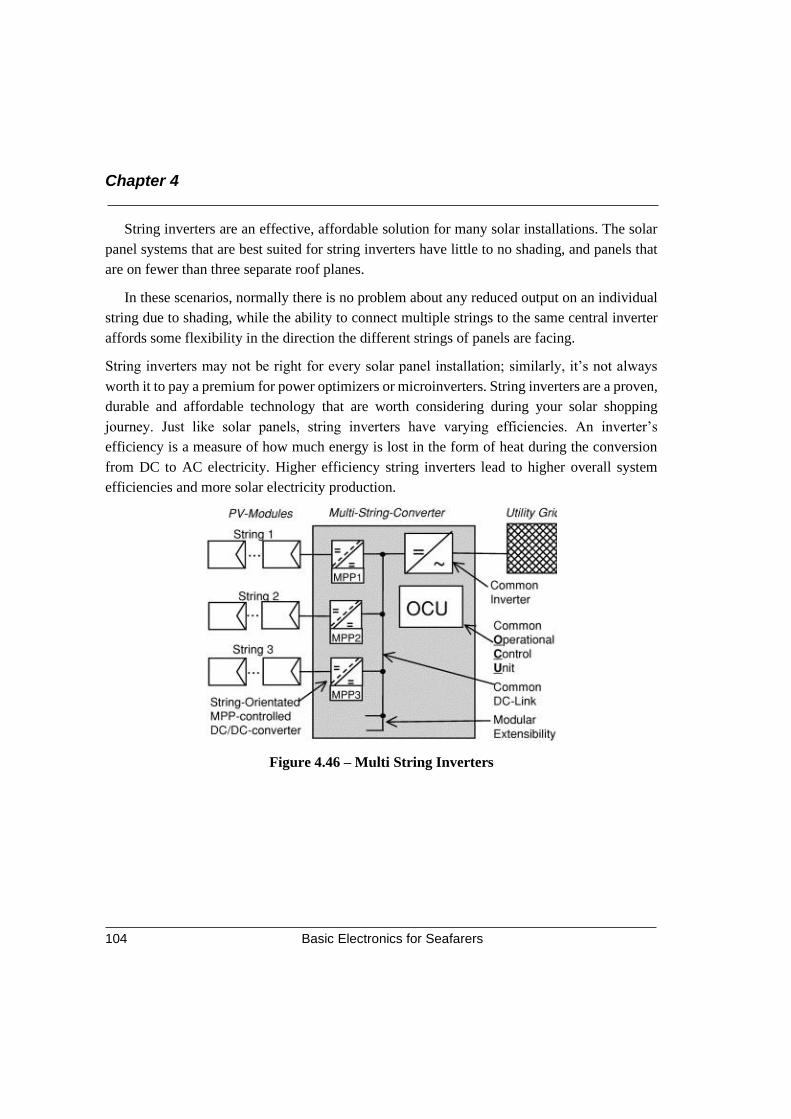
Chapter 4
Basic Electronics for Seafarers 104
String inverters are an effective, affordable solution for many solar installations. The solar
panel systems that are best suited for string inverters have little to no shading, and panels that
are on fewer than three separate roof planes.
In these scenarios, normally there is no problem about any reduced output on an individual
string due to shading, while the ability to connect multiple strings to the same central inverter
affords some flexibility in the direction the different strings of panels are facing.
String inverters may not be right for every solar panel installation; similarly, it’s not always
worth it to pay a premium for power optimizers or microinverters. String inverters are a proven,
durable and affordable technology that are worth considering during your solar shopping
journey. Just like solar panels, string inverters have varying efficiencies. An inverter’s
efficiency is a measure of how much energy is lost in the form of heat during the conversion
from DC to AC electricity. Higher efficiency string inverters lead to higher overall system
efficiencies and more solar electricity production.
Figure 4.46 – Multi String Inverters
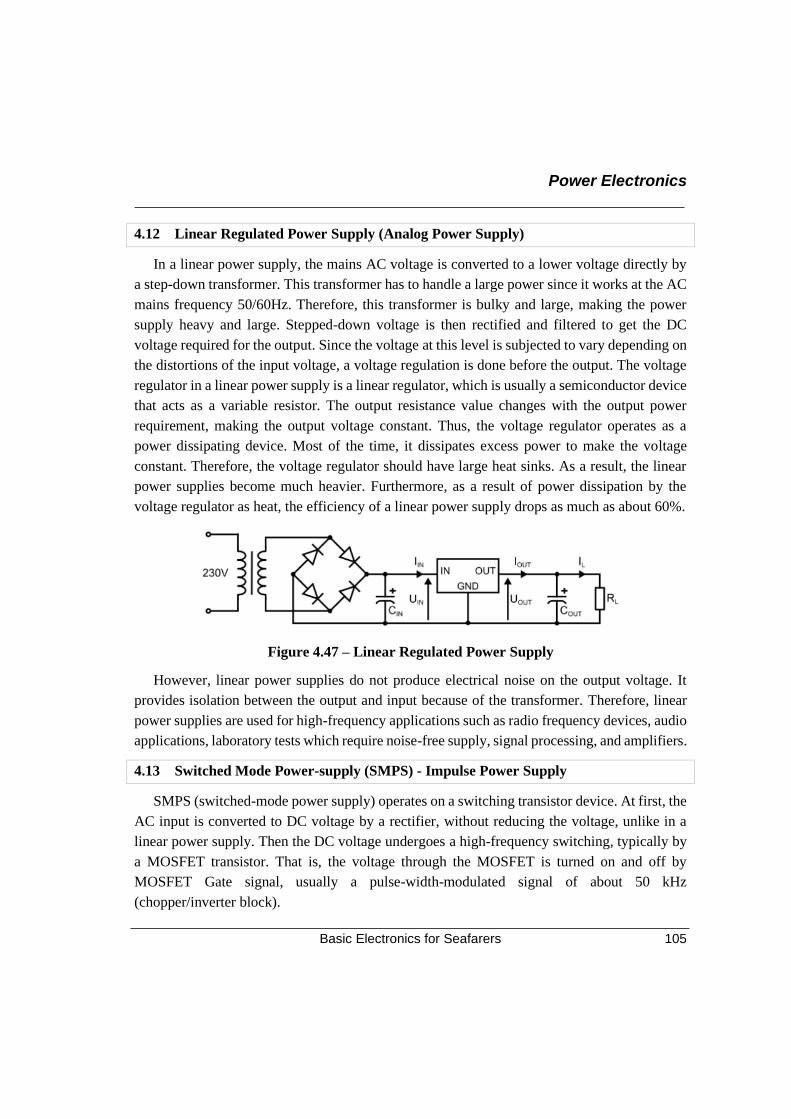
Power Electronics
Basic Electronics for Seafarers 105
4.12 Linear Regulated Power Supply (Analog Power Supply)
In a linear power supply, the mains AC voltage is converted to a lower voltage directly by
a step-down transformer. This transformer has to handle a large power since it works at the AC
mains frequency 50/60Hz. Therefore, this transformer is bulky and large, making the power
supply heavy and large. Stepped-down voltage is then rectified and filtered to get the DC
voltage required for the output. Since the voltage at this level is subjected to vary depending on
the distortions of the input voltage, a voltage regulation is done before the output. The voltage
regulator in a linear power supply is a linear regulator, which is usually a semiconductor device
that acts as a variable resistor. The output resistance value changes with the output power
requirement, making the output voltage constant. Thus, the voltage regulator operates as a
power dissipating device. Most of the time, it dissipates excess power to make the voltage
constant. Therefore, the voltage regulator should have large heat sinks. As a result, the linear
power supplies become much heavier. Furthermore, as a result of power dissipation by the
voltage regulator as heat, the efficiency of a linear power supply drops as much as about 60%.
Figure 4.47 – Linear Regulated Power Supply
However, linear power supplies do not produce electrical noise on the output voltage. It
provides isolation between the output and input because of the transformer. Therefore, linear
power supplies are used for high-frequency applications such as radio frequency devices, audio
applications, laboratory tests which require noise-free supply, signal processing, and amplifiers.
4.13 Switched Mode Power-supply (SMPS) - Impulse Power Supply
SMPS (switched-mode power supply) operates on a switching transistor device. At first, the
AC input is converted to DC voltage by a rectifier, without reducing the voltage, unlike in a
linear power supply. Then the DC voltage undergoes a high-frequency switching, typically by
a MOSFET transistor. That is, the voltage through the MOSFET is turned on and off by
MOSFET Gate signal, usually a pulse-width-modulated signal of about 50 kHz
(chopper/inverter block).
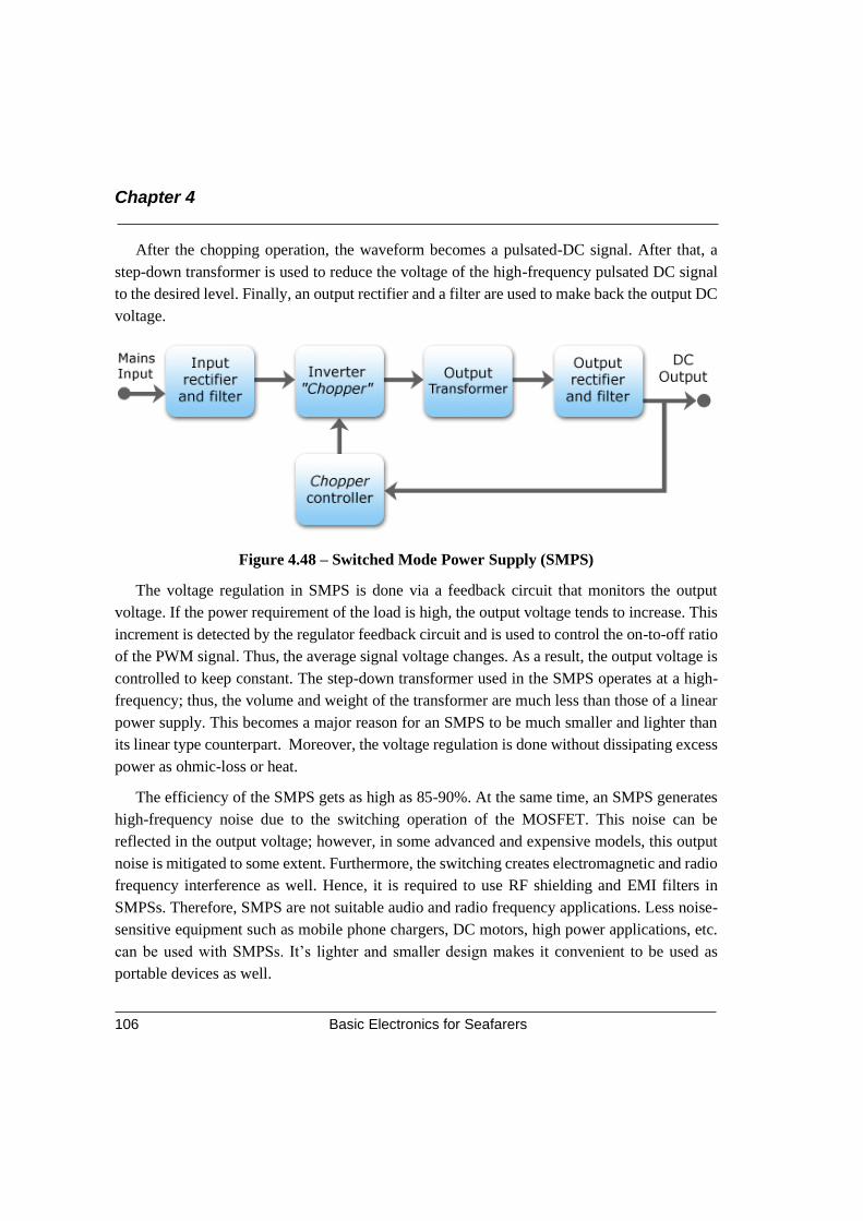
Chapter 4
Basic Electronics for Seafarers 106
After the chopping operation, the waveform becomes a pulsated-DC signal. After that, a
step-down transformer is used to reduce the voltage of the high-frequency pulsated DC signal
to the desired level. Finally, an output rectifier and a filter are used to make back the output DC
voltage.
Figure 4.48 – Switched Mode Power Supply (SMPS)
The voltage regulation in SMPS is done via a feedback circuit that monitors the output
voltage. If the power requirement of the load is high, the output voltage tends to increase. This
increment is detected by the regulator feedback circuit and is used to control the on-to-off ratio
of the PWM signal. Thus, the average signal voltage changes. As a result, the output voltage is
controlled to keep constant. The step-down transformer used in the SMPS operates at a high-
frequency; thus, the volume and weight of the transformer are much less than those of a linear
power supply. This becomes a major reason for an SMPS to be much smaller and lighter than
its linear type counterpart. Moreover, the voltage regulation is done without dissipating excess
power as ohmic-loss or heat.
The efficiency of the SMPS gets as high as 85-90%. At the same time, an SMPS generates
high-frequency noise due to the switching operation of the MOSFET. This noise can be
reflected in the output voltage; however, in some advanced and expensive models, this output
noise is mitigated to some extent. Furthermore, the switching creates electromagnetic and radio
frequency interference as well. Hence, it is required to use RF shielding and EMI filters in
SMPSs. Therefore, SMPS are not suitable audio and radio frequency applications. Less noise-
sensitive equipment such as mobile phone chargers, DC motors, high power applications, etc.
can be used with SMPSs. It’s lighter and smaller design makes it convenient to be used as
portable devices as well.
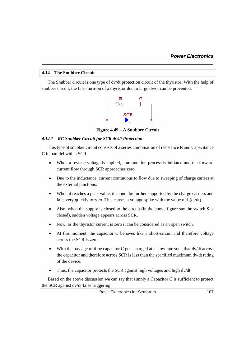
Power Electronics
Basic Electronics for Seafarers 107
4.14 The Snubber Circuit
The Snubber circuit is one type of dv/dt protection circuit of the thyristor. With the help of
snubber circuit, the false turn-on of a thyristor due to large dv/dt can be prevented.
Figure 4.49 – A Snubber Circuit
4.14.1 RC Snubber Circuit for SCR dv/dt Protection
This type of snubber circuit consists of a series combination of resistance R and Capacitance
C in parallel with a SCR.
• When a reverse voltage is applied, commutation process is initiated and the forward
current flow through SCR approaches zero.
• Due to the inductance, current continuous to flow due to sweeping of charge carries at
the external junctions.
• When it reaches a peak value, it cannot be further supported by the charge carriers and
falls very quickly to zero. This causes a voltage spike with the value of L(di/dt).
• Also, when the supply is closed to the circuit (in the above figure say the switch S is
closed), sudden voltage appears across SCR.
• Now, as the thyristor current is zero it can be considered as an open switch.
• At this moment, the capacitor C behaves like a short-circuit and therefore voltage
across the SCR is zero.
• With the passage of time capacitor C gets charged at a slow rate such that dv/dt across
the capacitor and therefore across SCR is less than the specified maximum dv/dt rating
of the device.
• Thus, the capacitor protects the SCR against high voltages and high dv/dt.
Based on the above discussion we can say that simply a Capacitor C is sufficient to protect
the SCR against dv/dt false triggering.
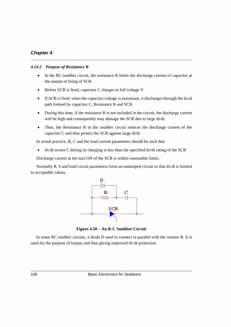
Chapter 4
Basic Electronics for Seafarers 108
4.14.2 Purpose of Resistance R
• In the RC snubber circuit, the resistance R limits the discharge current of capacitor at
the instant of firing of SCR.
• Before SCR is fired, capacitor C charges to full voltage V.
• If SCR is fired, when the capacitor voltage is maximum, it discharges through the local
path formed by capacitor C, Resistance R and SCR.
• During this time, if the resistance R is not included in the circuit, the discharge current
will be high and consequently may damage the SCR due to large di/dt.
• Thus, the Resistance R in the snubber circuit reduces the discharge current of the
capacitor C and thus protect the SCR against large di/dt.
In actual practice, R, C and the load current parameters should be such that
• dv/dt across C during its charging is less than the specified dv/dt rating of the SCR
Discharge current at the turn ON of the SCR is within reasonable limits.
Normally R, S and load circuit parameters form an undamped circuit so that dv/dt is limited
to acceptable values.
Figure 4.50 – An R-C Snubber Circuit
In some RC snubber circuits, a diode D used to connect in parallel with the resistor R. It is
used for the purpose of bypass and thus giving improved dv/dt protection.
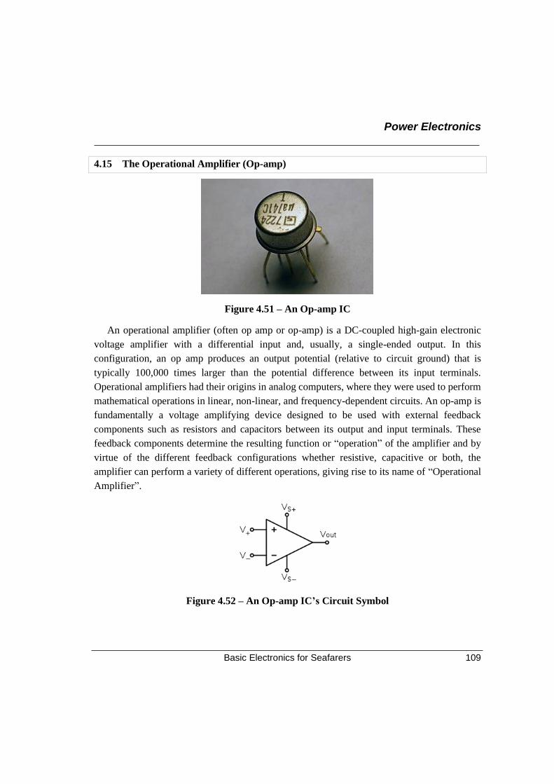
Power Electronics
Basic Electronics for Seafarers 109
4.15 The Operational Amplifier (Op-amp)
Figure 4.51 – An Op-amp IC
An operational amplifier (often op amp or op-amp) is a DC-coupled high-gain electronic
voltage amplifier with a differential input and, usually, a single-ended output. In this
configuration, an op amp produces an output potential (relative to circuit ground) that is
typically 100,000 times larger than the potential difference between its input terminals.
Operational amplifiers had their origins in analog computers, where they were used to perform
mathematical operations in linear, non-linear, and frequency-dependent circuits. An op-amp is
fundamentally a voltage amplifying device designed to be used with external feedback
components such as resistors and capacitors between its output and input terminals. These
feedback components determine the resulting function or “operation” of the amplifier and by
virtue of the different feedback configurations whether resistive, capacitive or both, the
amplifier can perform a variety of different operations, giving rise to its name of “Operational
Amplifier”.
Figure 4.52 – An Op-amp IC’s Circuit Symbol
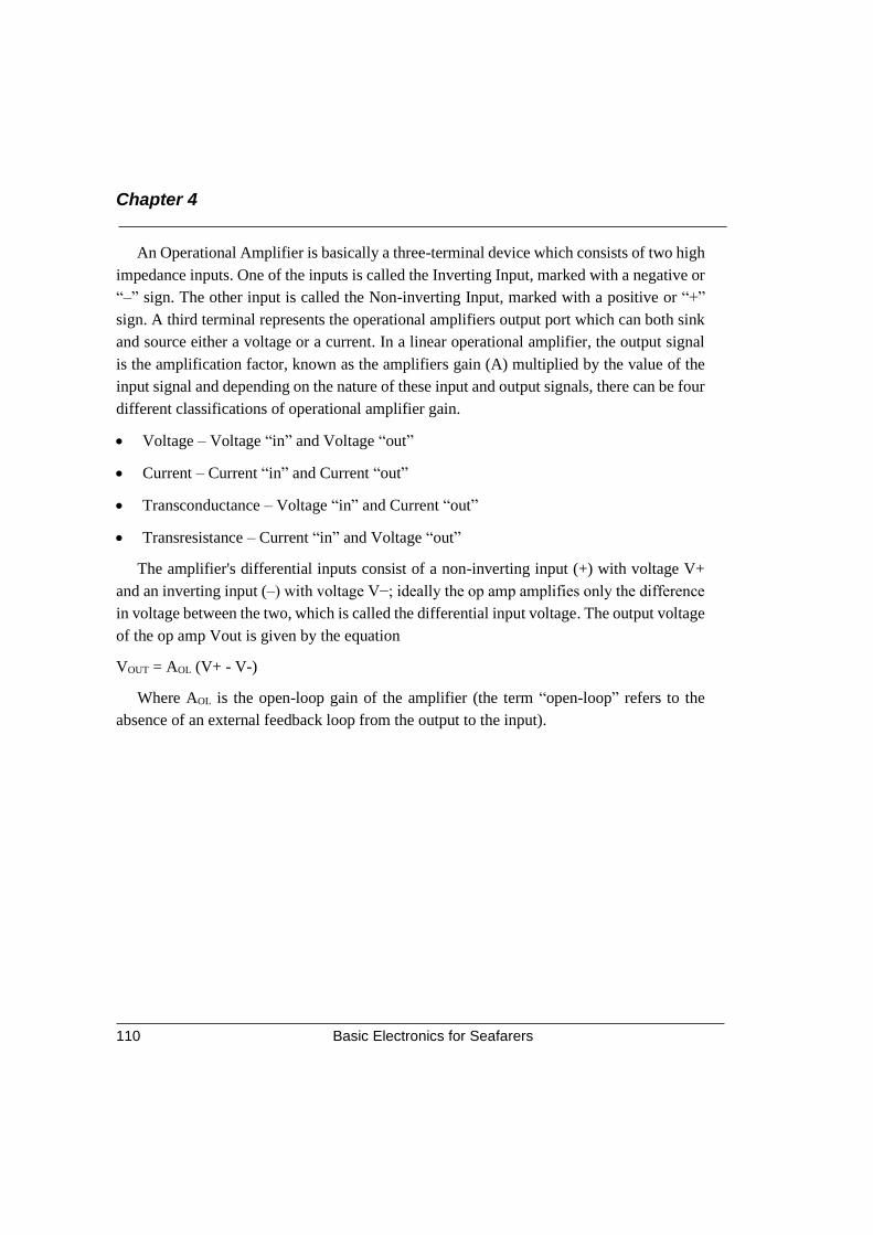
Chapter 4
Basic Electronics for Seafarers 110
An Operational Amplifier is basically a three-terminal device which consists of two high
impedance inputs. One of the inputs is called the Inverting Input, marked with a negative or
“–” sign. The other input is called the Non-inverting Input, marked with a positive or “+”
sign. A third terminal represents the operational amplifiers output port which can both sink
and source either a voltage or a current. In a linear operational amplifier, the output signal
is the amplification factor, known as the amplifiers gain (A) multiplied by the value of the
input signal and depending on the nature of these input and output signals, there can be four
different classifications of operational amplifier gain.
• Voltage – Voltage “in” and Voltage “out”
• Current – Current “in” and Current “out”
• Transconductance – Voltage “in” and Current “out”
• Transresistance – Current “in” and Voltage “out”
The amplifier's differential inputs consist of a non-inverting input (+) with voltage V+
and an inverting input (–) with voltage V−; ideally the op amp amplifies only the difference
in voltage between the two, which is called the differential input voltage. The output voltage
of the op amp Vout is given by the equation
VOUT = AOL (V+ - V-)
Where AOL is the open-loop gain of the amplifier (the term “open-loop” refers to the
absence of an external feedback loop from the output to the input).
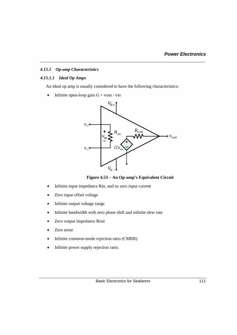
Power Electronics
Basic Electronics for Seafarers 111
4.15.1 Op-amp Characteristics
4.15.1.1 Ideal Op Amps
An ideal op amp is usually considered to have the following characteristics:
• Infinite open-loop gain G = vout / vin
Figure 4.53 – An Op-amp’s Equivalent Circuit
• Infinite input impedance Rin, and so zero input current
• Zero input offset voltage
• Infinite output voltage range
• Infinite bandwidth with zero phase shift and infinite slew rate
• Zero output impedance Rout
• Zero noise
• Infinite common-mode rejection ratio (CMRR)
• Infinite power supply rejection ratio.
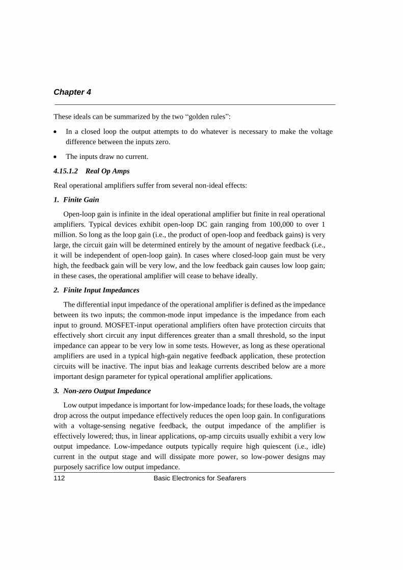
Chapter 4
Basic Electronics for Seafarers 112
These ideals can be summarized by the two “golden rules”:
• In a closed loop the output attempts to do whatever is necessary to make the voltage
difference between the inputs zero.
• The inputs draw no current.
4.15.1.2 Real Op Amps
Real operational amplifiers suffer from several non-ideal effects:
1. Finite Gain
Open-loop gain is infinite in the ideal operational amplifier but finite in real operational
amplifiers. Typical devices exhibit open-loop DC gain ranging from 100,000 to over 1
million. So long as the loop gain (i.e., the product of open-loop and feedback gains) is very
large, the circuit gain will be determined entirely by the amount of negative feedback (i.e.,
it will be independent of open-loop gain). In cases where closed-loop gain must be very
high, the feedback gain will be very low, and the low feedback gain causes low loop gain;
in these cases, the operational amplifier will cease to behave ideally.
2. Finite Input Impedances
The differential input impedance of the operational amplifier is defined as the impedance
between its two inputs; the common-mode input impedance is the impedance from each
input to ground. MOSFET-input operational amplifiers often have protection circuits that
effectively short circuit any input differences greater than a small threshold, so the input
impedance can appear to be very low in some tests. However, as long as these operational
amplifiers are used in a typical high-gain negative feedback application, these protection
circuits will be inactive. The input bias and leakage currents described below are a more
important design parameter for typical operational amplifier applications.
3. Non-zero Output Impedance
Low output impedance is important for low-impedance loads; for these loads, the voltage
drop across the output impedance effectively reduces the open loop gain. In configurations
with a voltage-sensing negative feedback, the output impedance of the amplifier is
effectively lowered; thus, in linear applications, op-amp circuits usually exhibit a very low
output impedance. Low-impedance outputs typically require high quiescent (i.e., idle)
current in the output stage and will dissipate more power, so low-power designs may
purposely sacrifice low output impedance.
Power Electronics
Basic Electronics for Seafarers 113
4. Input Current
Due to biasing requirements or leakage, a small amount of current (typically ~10
nanoamperes for bipolar op amps, tens of picoamperes for JFET input stages, and only a few
pA for MOSFET input stages) flows into the inputs. When large resistors or sources with high
output impedances are used in the circuit, these small currents can produce large unmodeled
voltage drops. If the input currents are matched, and the impedance looking out of both inputs
are matched, then the voltages produced at each input will be equal. Because the operational
amplifier operates on the difference between its inputs, these matched voltages will have no
effect. It is more common for the input currents to be slightly mismatched. The difference is
called input offset current, and even with matched resistances a small offset voltage (different
from the input offset voltage below) can be produced. This offset voltage can create offsets or
drifting in the operational amplifier.
5. Input Offset Voltage
This voltage, which is what, is required across the op amp's input terminals to drive the
output voltage to zero. In the perfect amplifier, there would be no input offset voltage.
However, it exists in actual op amps because of imperfections in the differential amplifier that
constitutes the input stage of the vast majority of these devices. Input offset voltage creates two
problems: First, due to the amplifier's high voltage gain, it virtually assures that the amplifier
output will go into saturation if it is operated without negative feedback, even when the input
terminals are wired together. Second, in a closed loop, negative feedback configuration, the
input offset voltage is amplified along with the signal and this may pose a problem if high
precision DC amplification is required or if the input signal is very small.
6. Common-mode Gain
A perfect operational amplifier amplifies only the voltage difference between its two inputs,
completely rejecting all voltages that are common to both. However, the differential input stage
of an operational amplifier is never perfect, leading to the amplification of these common
voltages to some degree. The standard measure of this defect is called the common-mode
rejection ratio (denoted CMRR). Minimization of common mode gain is usually important in
non-inverting amplifiers (described below) that operate at high amplification.
Chapter 4
Basic Electronics for Seafarers 114
7. Power-supply Rejection
The output of a perfect operational amplifier will be completely independent from its
power supply. Every real operational amplifier has a finite power supply rejection ratio
(PSRR) that reflects how well the op amp can reject changes in its supply voltage.
8. Finite Bandwidth
All amplifiers have finite bandwidth. To a first approximation, the op amp has the
frequency response of an integrator with gain. That is, the gain of a typical op amp is
inversely proportional to frequency and is characterized by its gain–bandwidth product
(GBWP). For example, an op amp with a GBWP of 1 MHz would have a gain of 5 at 200
kHz, and a gain of 1 at 1 MHz. This dynamic response coupled with the very high DC gain
of the op amp gives it the characteristics of a first-order low-pass filter with very high DC
gain and low cutoff frequency given by the GBWP divided by the DC gain.
9. Non-Linear Input-Output Relationship
The output voltage may not be accurately proportional to the difference between the
input voltages. It is commonly called distortion when the input signal is a waveform. This
effect will be very small in a practical circuit where substantial negative feedback is used.
10. Limited Output Current
The output current must be finite. In practice, most op amps are designed to limit the
output current so as not to exceed a specified level – around 25 mA for a type 741 IC op
amp – thus protecting the op amp and associated circuitry from damage. Modern designs
are electronically more rugged than earlier implementations and some can sustain direct
short circuits on their outputs without damage.
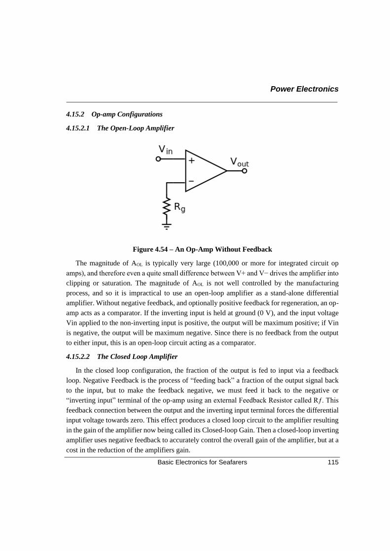
Power Electronics
Basic Electronics for Seafarers 115
4.15.2 Op-amp Configurations
4.15.2.1 The Open-Loop Amplifier
Figure 4.54 – An Op-Amp Without Feedback
The magnitude of AOL is typically very large (100,000 or more for integrated circuit op
amps), and therefore even a quite small difference between V+ and V− drives the amplifier into
clipping or saturation. The magnitude of AOL is not well controlled by the manufacturing
process, and so it is impractical to use an open-loop amplifier as a stand-alone differential
amplifier. Without negative feedback, and optionally positive feedback for regeneration, an op-
amp acts as a comparator. If the inverting input is held at ground (0 V), and the input voltage
Vin applied to the non-inverting input is positive, the output will be maximum positive; if Vin
is negative, the output will be maximum negative. Since there is no feedback from the output
to either input, this is an open-loop circuit acting as a comparator.
4.15.2.2 The Closed Loop Amplifier
In the closed loop configuration, the fraction of the output is fed to input via a feedback
loop. Negative Feedback is the process of “feeding back” a fraction of the output signal back
to the input, but to make the feedback negative, we must feed it back to the negative or
“inverting input” terminal of the op-amp using an external Feedback Resistor called Rƒ. This
feedback connection between the output and the inverting input terminal forces the differential
input voltage towards zero. This effect produces a closed loop circuit to the amplifier resulting
in the gain of the amplifier now being called its Closed-loop Gain. Then a closed-loop inverting
amplifier uses negative feedback to accurately control the overall gain of the amplifier, but at a
cost in the reduction of the amplifiers gain.
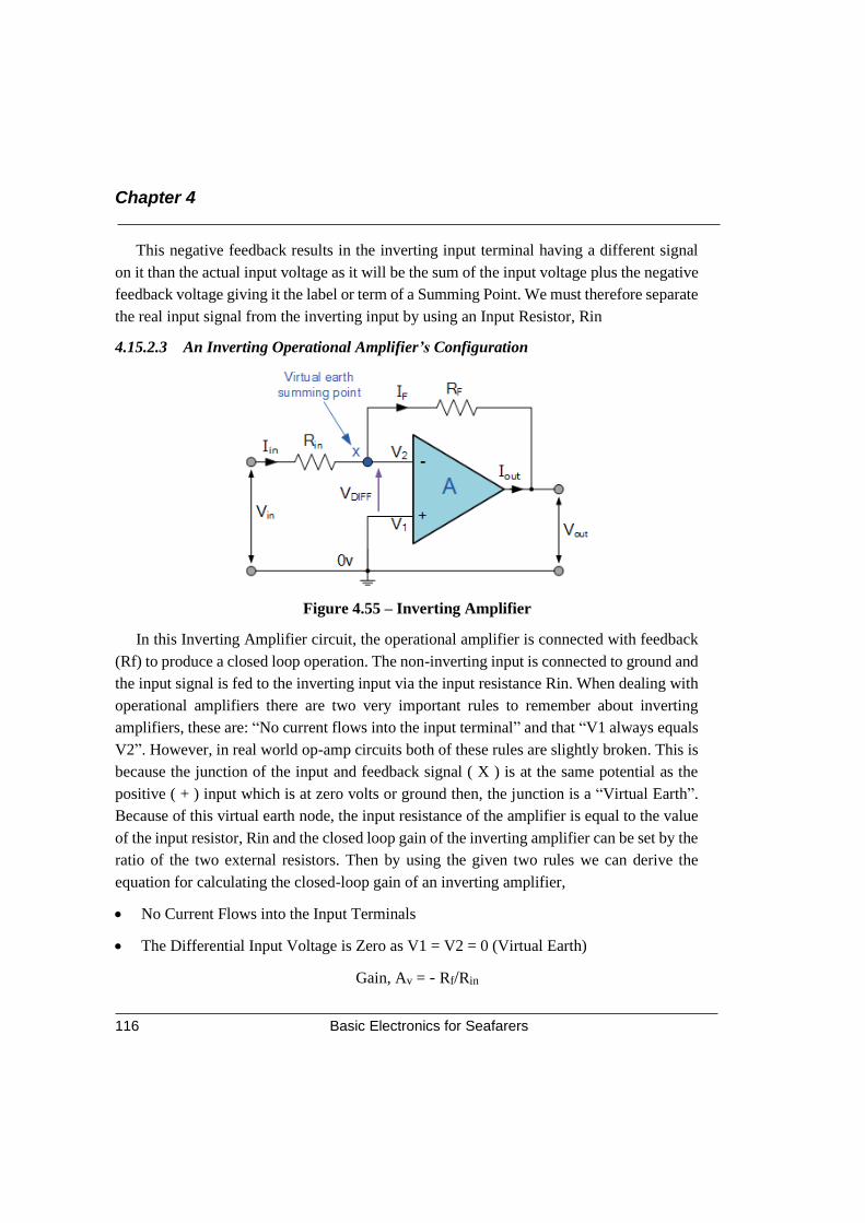
Chapter 4
Basic Electronics for Seafarers 116
This negative feedback results in the inverting input terminal having a different signal
on it than the actual input voltage as it will be the sum of the input voltage plus the negative
feedback voltage giving it the label or term of a Summing Point. We must therefore separate
the real input signal from the inverting input by using an Input Resistor, Rin
4.15.2.3 An Inverting Operational Amplifier’s Configuration
Figure 4.55 – Inverting Amplifier
In this Inverting Amplifier circuit, the operational amplifier is connected with feedback
(Rf) to produce a closed loop operation. The non-inverting input is connected to ground and
the input signal is fed to the inverting input via the input resistance Rin. When dealing with
operational amplifiers there are two very important rules to remember about inverting
amplifiers, these are: “No current flows into the input terminal” and that “V1 always equals
V2”. However, in real world op-amp circuits both of these rules are slightly broken. This is
because the junction of the input and feedback signal ( X ) is at the same potential as the
positive ( + ) input which is at zero volts or ground then, the junction is a “Virtual Earth”.
Because of this virtual earth node, the input resistance of the amplifier is equal to the value
of the input resistor, Rin and the closed loop gain of the inverting amplifier can be set by the
ratio of the two external resistors. Then by using the given two rules we can derive the
equation for calculating the closed-loop gain of an inverting amplifier,
• No Current Flows into the Input Terminals
• The Differential Input Voltage is Zero as V1 = V2 = 0 (Virtual Earth)
Gain, Av = - Rf/Rin
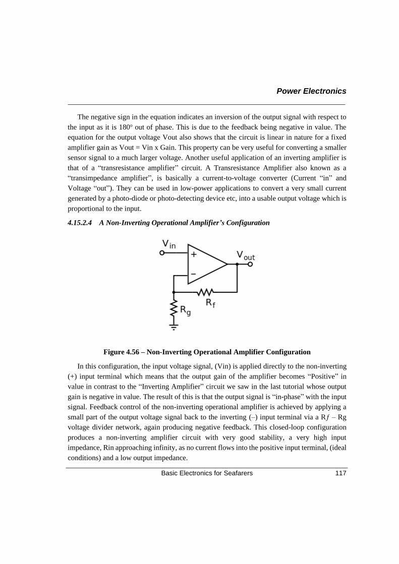
Power Electronics
Basic Electronics for Seafarers 117
The negative sign in the equation indicates an inversion of the output signal with respect to
the input as it is 180o out of phase. This is due to the feedback being negative in value. The
equation for the output voltage Vout also shows that the circuit is linear in nature for a fixed
amplifier gain as Vout = Vin x Gain. This property can be very useful for converting a smaller
sensor signal to a much larger voltage. Another useful application of an inverting amplifier is
that of a “transresistance amplifier” circuit. A Transresistance Amplifier also known as a
“transimpedance amplifier”, is basically a current-to-voltage converter (Current “in” and
Voltage “out”). They can be used in low-power applications to convert a very small current
generated by a photo-diode or photo-detecting device etc, into a usable output voltage which is
proportional to the input.
4.15.2.4 A Non-Inverting Operational Amplifier’s Configuration
Figure 4.56 – Non-Inverting Operational Amplifier Configuration
In this configuration, the input voltage signal, (Vin) is applied directly to the non-inverting
(+) input terminal which means that the output gain of the amplifier becomes “Positive” in
value in contrast to the “Inverting Amplifier” circuit we saw in the last tutorial whose output
gain is negative in value. The result of this is that the output signal is “in-phase” with the input
signal. Feedback control of the non-inverting operational amplifier is achieved by applying a
small part of the output voltage signal back to the inverting (–) input terminal via a Rƒ – Rg
voltage divider network, again producing negative feedback. This closed-loop configuration
produces a non-inverting amplifier circuit with very good stability, a very high input
impedance, Rin approaching infinity, as no current flows into the positive input terminal, (ideal
conditions) and a low output impedance.
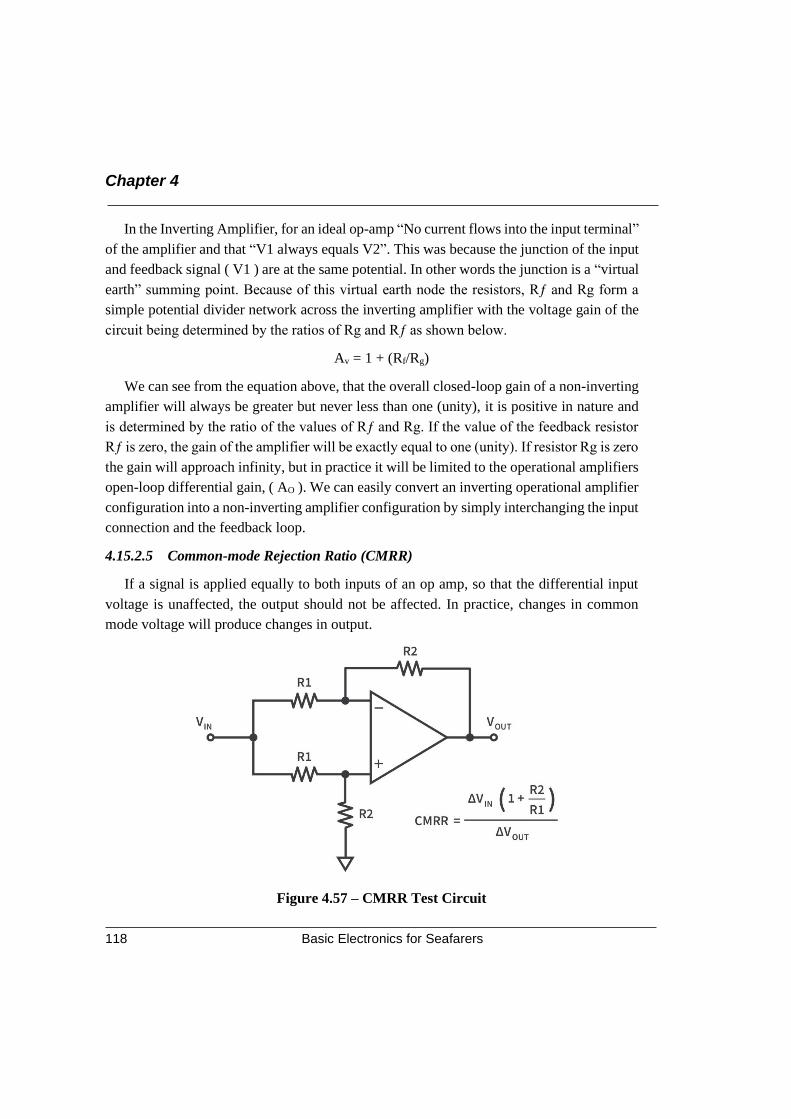
Chapter 4
Basic Electronics for Seafarers 118
In the Inverting Amplifier, for an ideal op-amp “No current flows into the input terminal”
of the amplifier and that “V1 always equals V2”. This was because the junction of the input
and feedback signal ( V1 ) are at the same potential. In other words the junction is a “virtual
earth” summing point. Because of this virtual earth node the resistors, Rƒ and Rg form a
simple potential divider network across the inverting amplifier with the voltage gain of the
circuit being determined by the ratios of Rg and Rƒ as shown below.
Av = 1 + (Rf/Rg)
We can see from the equation above, that the overall closed-loop gain of a non-inverting
amplifier will always be greater but never less than one (unity), it is positive in nature and
is determined by the ratio of the values of Rƒ and Rg. If the value of the feedback resistor
Rƒ is zero, the gain of the amplifier will be exactly equal to one (unity). If resistor Rg is zero
the gain will approach infinity, but in practice it will be limited to the operational amplifiers
open-loop differential gain, ( AO ). We can easily convert an inverting operational amplifier
configuration into a non-inverting amplifier configuration by simply interchanging the input
connection and the feedback loop.
4.15.2.5 Common-mode Rejection Ratio (CMRR)
If a signal is applied equally to both inputs of an op amp, so that the differential input
voltage is unaffected, the output should not be affected. In practice, changes in common
mode voltage will produce changes in output.
Figure 4.57 – CMRR Test Circuit
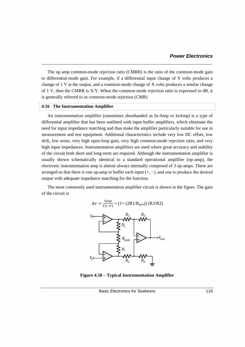
Power Electronics
Basic Electronics for Seafarers 119
The op amp common-mode rejection ratio (CMRR) is the ratio of the common-mode gain
to differential-mode gain. For example, if a differential input change of Y volts produces a
change of 1 V at the output, and a common-mode change of X volts produces a similar change
of 1 V, then the CMRR is X/Y. When the common-mode rejection ratio is expressed in dB, it
is generally referred to as common-mode rejection (CMR)
4.16 The Instrumentation Amplifier
An instrumentation amplifier (sometimes shorthanded as In-Amp or InAmp) is a type of
differential amplifier that has been outfitted with input buffer amplifiers, which eliminate the
need for input impedance matching and thus make the amplifier particularly suitable for use in
measurement and test equipment. Additional characteristics include very low DC offset, low
drift, low noise, very high open-loop gain, very high common-mode rejection ratio, and very
high input impedances. Instrumentation amplifiers are used where great accuracy and stability
of the circuit both short and long-term are required. Although the instrumentation amplifier is
usually shown schematically identical to a standard operational amplifier (op-amp), the
electronic instrumentation amp is almost always internally composed of 3 op-amps. These are
arranged so that there is one op-amp to buffer each input (+, −), and one to produce the desired
output with adequate impedance matching for the function.
The most commonly used instrumentation amplifier circuit is shown in the figure. The gain
of the circuit is
𝐴𝑣 =Vout
𝑉2−𝑉1 = (1+ (2R1/Rgain)) (R3/R2)
Figure 4.58 – Typical Instrumentation Amplifier
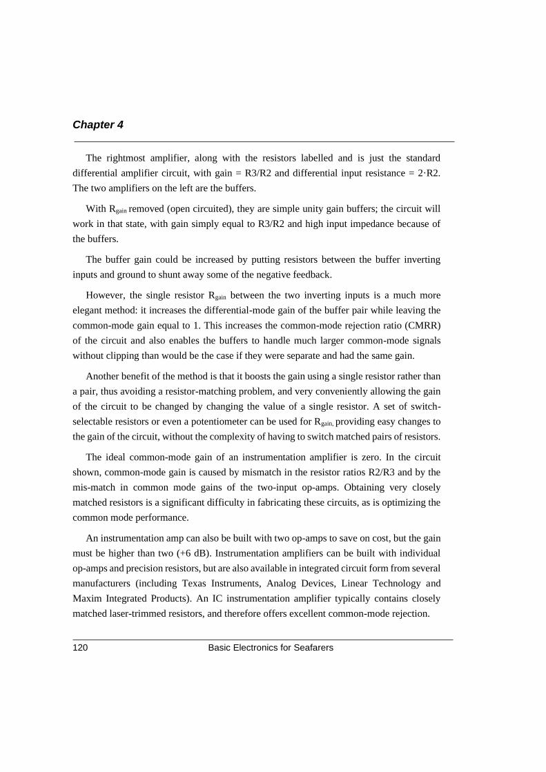
Chapter 4
Basic Electronics for Seafarers 120
The rightmost amplifier, along with the resistors labelled and is just the standard
differential amplifier circuit, with gain = R3/R2 and differential input resistance = 2·R2.
The two amplifiers on the left are the buffers.
With Rgain removed (open circuited), they are simple unity gain buffers; the circuit will
work in that state, with gain simply equal to R3/R2 and high input impedance because of
the buffers.
The buffer gain could be increased by putting resistors between the buffer inverting
inputs and ground to shunt away some of the negative feedback.
However, the single resistor Rgain between the two inverting inputs is a much more
elegant method: it increases the differential-mode gain of the buffer pair while leaving the
common-mode gain equal to 1. This increases the common-mode rejection ratio (CMRR)
of the circuit and also enables the buffers to handle much larger common-mode signals
without clipping than would be the case if they were separate and had the same gain.
Another benefit of the method is that it boosts the gain using a single resistor rather than
a pair, thus avoiding a resistor-matching problem, and very conveniently allowing the gain
of the circuit to be changed by changing the value of a single resistor. A set of switch-
selectable resistors or even a potentiometer can be used for Rgain, providing easy changes to
the gain of the circuit, without the complexity of having to switch matched pairs of resistors.
The ideal common-mode gain of an instrumentation amplifier is zero. In the circuit
shown, common-mode gain is caused by mismatch in the resistor ratios R2/R3 and by the
mis-match in common mode gains of the two-input op-amps. Obtaining very closely
matched resistors is a significant difficulty in fabricating these circuits, as is optimizing the
common mode performance.
An instrumentation amp can also be built with two op-amps to save on cost, but the gain
must be higher than two (+6 dB). Instrumentation amplifiers can be built with individual
op-amps and precision resistors, but are also available in integrated circuit form from several
manufacturers (including Texas Instruments, Analog Devices, Linear Technology and
Maxim Integrated Products). An IC instrumentation amplifier typically contains closely
matched laser-trimmed resistors, and therefore offers excellent common-mode rejection.
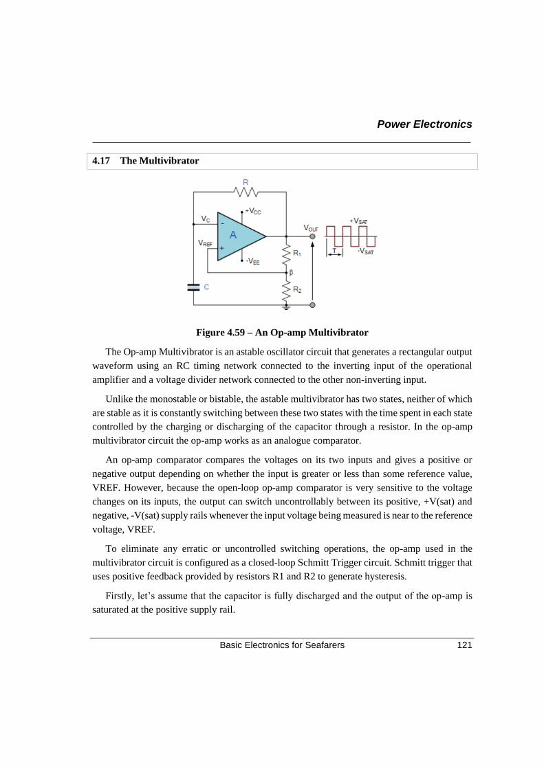
Power Electronics
Basic Electronics for Seafarers 121
4.17 The Multivibrator
Figure 4.59 – An Op-amp Multivibrator
The Op-amp Multivibrator is an astable oscillator circuit that generates a rectangular output
waveform using an RC timing network connected to the inverting input of the operational
amplifier and a voltage divider network connected to the other non-inverting input.
Unlike the monostable or bistable, the astable multivibrator has two states, neither of which
are stable as it is constantly switching between these two states with the time spent in each state
controlled by the charging or discharging of the capacitor through a resistor. In the op-amp
multivibrator circuit the op-amp works as an analogue comparator.
An op-amp comparator compares the voltages on its two inputs and gives a positive or
negative output depending on whether the input is greater or less than some reference value,
VREF. However, because the open-loop op-amp comparator is very sensitive to the voltage
changes on its inputs, the output can switch uncontrollably between its positive, +V(sat) and
negative, -V(sat) supply rails whenever the input voltage being measured is near to the reference
voltage, VREF.
To eliminate any erratic or uncontrolled switching operations, the op-amp used in the
multivibrator circuit is configured as a closed-loop Schmitt Trigger circuit. Schmitt trigger that
uses positive feedback provided by resistors R1 and R2 to generate hysteresis.
Firstly, let’s assume that the capacitor is fully discharged and the output of the op-amp is
saturated at the positive supply rail.
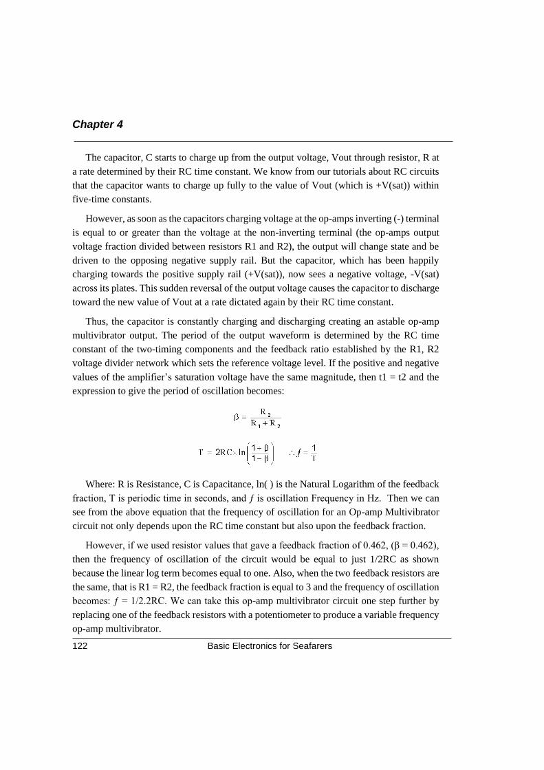
Chapter 4
Basic Electronics for Seafarers 122
The capacitor, C starts to charge up from the output voltage, Vout through resistor, R at
a rate determined by their RC time constant. We know from our tutorials about RC circuits
that the capacitor wants to charge up fully to the value of Vout (which is +V(sat)) within
five-time constants.
However, as soon as the capacitors charging voltage at the op-amps inverting (-) terminal
is equal to or greater than the voltage at the non-inverting terminal (the op-amps output
voltage fraction divided between resistors R1 and R2), the output will change state and be
driven to the opposing negative supply rail. But the capacitor, which has been happily
charging towards the positive supply rail (+V(sat)), now sees a negative voltage, -V(sat)
across its plates. This sudden reversal of the output voltage causes the capacitor to discharge
toward the new value of Vout at a rate dictated again by their RC time constant.
Thus, the capacitor is constantly charging and discharging creating an astable op-amp
multivibrator output. The period of the output waveform is determined by the RC time
constant of the two-timing components and the feedback ratio established by the R1, R2
voltage divider network which sets the reference voltage level. If the positive and negative
values of the amplifier’s saturation voltage have the same magnitude, then t1 = t2 and the
expression to give the period of oscillation becomes:
Where: R is Resistance, C is Capacitance, ln( ) is the Natural Logarithm of the feedback
fraction, T is periodic time in seconds, and ƒ is oscillation Frequency in Hz. Then we can
see from the above equation that the frequency of oscillation for an Op-amp Multivibrator
circuit not only depends upon the RC time constant but also upon the feedback fraction.
However, if we used resistor values that gave a feedback fraction of 0.462, (β = 0.462),
then the frequency of oscillation of the circuit would be equal to just 1/2RC as shown
because the linear log term becomes equal to one. Also, when the two feedback resistors are
the same, that is R1 = R2, the feedback fraction is equal to 3 and the frequency of oscillation
becomes: ƒ = 1/2.2RC. We can take this op-amp multivibrator circuit one step further by
replacing one of the feedback resistors with a potentiometer to produce a variable frequency
op-amp multivibrator.
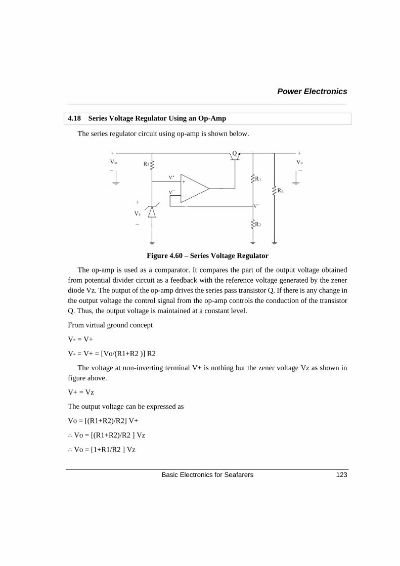
Power Electronics
Basic Electronics for Seafarers 123
4.18 Series Voltage Regulator Using an Op-Amp
The series regulator circuit using op-amp is shown below.
Figure 4.60 – Series Voltage Regulator
The op-amp is used as a comparator. It compares the part of the output voltage obtained
from potential divider circuit as a feedback with the reference voltage generated by the zener
diode Vz. The output of the op-amp drives the series pass transistor Q. If there is any change in
the output voltage the control signal from the op-amp controls the conduction of the transistor
Q. Thus, the output voltage is maintained at a constant level.
From virtual ground concept
V- = V+
V- = V+ = [Vo/(R1+R2 )] R2
The voltage at non-inverting terminal V+ is nothing but the zener voltage Vz as shown in
figure above.
V+ = Vz
The output voltage can be expressed as
Vo = [(R1+R2)/R2] V+
∴ Vo = [(R1+R2)/R2 ] Vz
∴ Vo = [1+R1/R2 ] Vz
Chapter 4
Basic Electronics for Seafarers 124
4.19 The 4-20 mA Current Loop Transmitter Using an Op-Amp
In instrumentation circuitry, DC signals are often used as analog representations of
physical measurements such as temperature, pressure, flow, weight, and motion. Most
commonly, DC current signals are used in preference to DC voltage signals, because current
signals are exactly equal in magnitude throughout the series circuit loop carrying current
from the source (measuring device) to the load (indicator, recorder, or controller), whereas
voltage signals in a parallel circuit may vary from one end to the other due to resistive wire
losses. Furthermore, current-sensing instruments typically have low impedances (while
voltage-sensing instruments have high impedances), which gives current-sensing
instruments greater electrical noise immunity.
Figure 4.61 – 4-20 mA Transmitter
The input voltage to this circuit is assumed to be coming from some type of physical
transducer/amplifier arrangement, calibrated to produce 1 volt at 0 percent of physical
measurement, and 5 volts at 100 percent of physical measurement. The standard analog
current signal range is 4 mA to 20 mA, signifying 0% to 100% of measurement range,
respectively. With a 5 volts input, the 250 Ω (precision) resistor will have 5 volts applied
across it, resulting in 20 mA of current in the large loop circuit (with Rload).
It does not matter what resistance value Rload is, or how much wire resistance is present
in that large loop, so long as the op-amp has a high enough power supply voltage to output
the voltage necessary to get 20 mA flowing through Rload.
Power Electronics
Basic Electronics for Seafarers 125
The 250 Ω resistor establishes the relationship between input voltage and output current, in
this case creating the equivalence of 1-5 V in / 4-20 mA out. If we were converting the 1–5-
volt input signal to a 10-50 mA output signal (an older, obsolete instrumentation standard for
industry), we’d use a 100 Ω precision resistor instead.

Chapter 4
Basic Electronics for Seafarers 126
Sources
• https://www.circuitstoday.com/
• https://en.wikipedia.org/
• https://www.electronics-notes.com/
• https://www.electrical4u.com/
• https://instrumentationtools.com/
• https://www.electronics-tutorials.ws/
• https://industrialcircuits.wordpress.com/
• https://www.circuitstoday.com/
• https://www.electronicshub.org/
• https://news.energysage.com/
• https://www.differencebetween.com/
In the end of this book. I would
like to take the opportunity to
thank all my readers. May all of
you achieve more and more in life.
All the best for your future. I
would like to convey a happy
message to all of you by a quote
by Swami Vivekanand that is close
to my heart, “Strength is Life,
Weakness is Death.
Expansion is Life, Contraction
is Death.
Love is Life, Hatred is Death.”
Thank You.

Chapter 5 ICs and LSI
Basic Electronics for Seafarers
Sir! I’ve always wondered how do
these Automatic Lighting,
Automatic Faucets and these
latest, so called, “cool” gadgets
work with minimal human
interference. I’m so much
fascinated to learn about it! Things
like IOT and AI just widen up my
eyes!
Divyam! What I believe is
that, if you want to master
any field. Then, you should
start with the small bits.
Try to break every big
thing you see infront of
you into its basics. In this
chapter I’m going to tell
you about the IC and LSI
techniques. You are also
going to learn that to
create BIG buildings you
need to create a strong
foundation first!
Chapter 5
Basic Electronics for Seafarers 128
5.1 Introduction
An electronic circuit is created by connecting different discrete components like resistors,
capacitors, transistors, mosfets, etc., by soldering them on a PCB (printed circuit board). But it
has lot of disadvantages - it consumes lot of space and the chance for a break down is very high
due to lots of soldering joints, so it is less reliable. To overcome these problems scientists,
developed a method to create the whole circuit into a single silicon chip to form a small package
called an Integrated Circuit or IC. That means every IC contain lots of discrete components and
they are connected in a manner to achieve a particular function. By this method, the cost and
space re easily reduced and also the reliability is greatly increased. ICs are now used in virtually
all electronic systems and have revolutionized the world of electronics. Computers, mobile
phones, and other digital home appliances are now inextricable parts of the structure of modern
societies, made possible by the small size and low cost of ICs.
5.1.1 Advantages of an IC
• The entire physical size of IC is extremely small than that of discrete circuit.
• The weight of an IC is very less as compared entire discrete circuits.
• It is more reliable.
• Lower power consumption.
• It can easily replace but it can hardly repair, in case of failure.
• High operating speed due to low parasitic capacitance.
• Temperature differences between components of a circuit are small.
• It has suitable for small signal operation.
• Low cost
5.1.2 Disadvantages of an IC
• It can handle only a limited amount of power.
• It is difficult to be achieved low temperature coefficient.
• The power dissipation is limited to 10 watts.
• Low noise and high voltage operation are not easily obtained.
• Inductors and transformers are needed connecting to exterior to the semiconductor chip
as it is not possible to fabricate inductor and transformers on the semiconductor chip
surface.
• Not repairable in the case of failure.
ICs and LSI
Basic Electronics for Seafarers 129
Semiconductor ICs are fabricated in a planar process which includes three key process steps
– photolithography, deposition (such as chemical vapour deposition), and etching. The main
process steps are supplemented by doping and cleaning. More recent or high-performance ICs
may instead the use of multi-gate FinFET or GAAFET transistors instead of planar ones,
starting at the 22 nm node (Intel) or 16/14 nm nodes.
Mono-crystal silicon wafers are used in most applications (or for special applications, other
semiconductors such as gallium arsenide are used). The wafer need not be entirely silicon.
Photolithography is used to mark different areas of the substrate to be doped or to have
polysilicon, insulators or metal (typically aluminium or copper) tracks deposited on them.
Dopants are impurities intentionally introduced to a semiconductor to modulate its electronic
properties. Doping is the process of adding dopants to a semiconductor material.
5.2 Fabrication
Integrated circuits are composed of many overlapping layers, each defined by
photolithography, and normally shown in different colors. Some layers mark where various
dopants are diffused into the substrate (called diffusion layers), some define where additional
ions are implanted (implant layers), some define the conductors (doped polysilicon or metal
layers), and some define the connections between the conducting layers (via or contact layers).
All components are constructed from a specific combination of these layers.
• In a self-aligned CMOS process, a transistor is formed wherever the gate layer
(polysilicon or metal) crosses a diffusion layer.
• Capacitive structures, in form very much like the parallel conducting plates of a
traditional electrical capacitor, are formed according to the area of the “plates”, with
insulating material between the plates. Capacitors of a wide range of sizes are common
on ICs.
• Meandering stripes of varying lengths are sometimes used to form on-chip resistors,
though most logic circuits do not need any resistors. The ratio of the length of the
resistive structure to its width, combined with its sheet resistivity, determines the
resistance.
• More rarely, inductive structures can be built as tiny on-chip coils, or simulated by
gyrators.
Chapter 5
Basic Electronics for Seafarers 130
There are different technologies to develop the ICs. These are indicating the different
generation of this process. Those are SSI, MSI, LSI, VLSI and ULSI. The comparison is
given below in the table.
Acronym Name Year Transistor count
SSI Small scale integration 1964 1-10
MSI Medium scale integration 1968 10-500
LSI Large scale integration 1971 500-20000
VLSI Very large-scale integration 1980 20000-1000000
ULSI Ultra large-scale integration 1984 >1000000
5.3 Large Scale Integration (LSI)
Large-scale integration (LSI) is the process of integrating or embedding thousands of
transistors on a single silicon semiconductor microchip. LSI technology was conceived in the
mid-1970s when computer processor microchips were under development. LSI is no longer in
use. It was succeeded by very large-scale integration (VLSI) and ultra large-scale integration
(ULSI) technologies.
5.4 Logic Gate Families
Logic Gates like NAND, NOR are used in daily applications for performing logic
operations. The Gates are manufactured using semiconductor devices like BJT, Diodes, or
FETs. Digital logic circuits are manufactured depending on the specific circuit technology or
logic families. The different logic families are RTL (Resistor Transistor Logic), DTL (Diode
Transistor Logic), TTL (Transistor-Transistor Logic), ECL (Emitter Coupled Logic) and
CMOS (Complementary Metal Oxide Semiconductor Logic). Out of these, RTL and DTL are
rarely used. Here we discuss about Transistor-Transistor Logic (TTL) and Emitter Coupled
Logic (ECL).
5.5 TTL (Transistor Transistor Logic)
The TTL or Transistor-Transistor Logic was invented in the year 1961 by “James L. Buie
of TRW”. It is suitable for developing new integrated circuits. The actual name of this TTL is
TCTL which means transistor-coupled transistor logic. After their introduction in integrated
circuit form in 1963 by Sylvania Electric Products, TTL integrated circuits were manufactured
by several semiconductor companies. The 7400 series by Texas Instruments became
particularly popular.
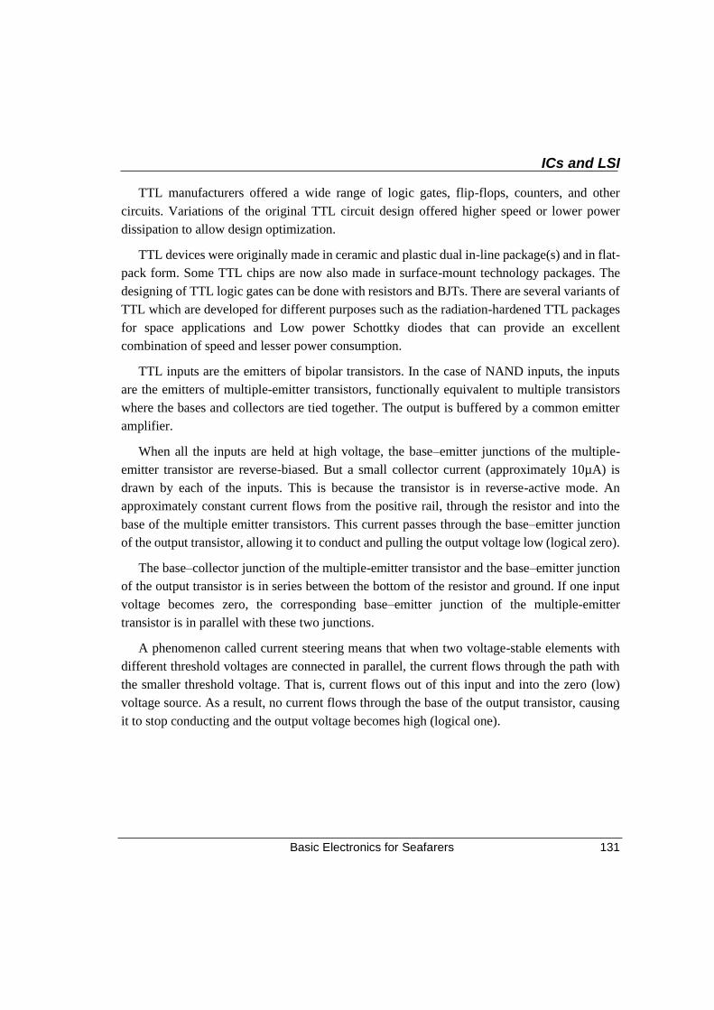
ICs and LSI
Basic Electronics for Seafarers 131
TTL manufacturers offered a wide range of logic gates, flip-flops, counters, and other
circuits. Variations of the original TTL circuit design offered higher speed or lower power
dissipation to allow design optimization.
TTL devices were originally made in ceramic and plastic dual in-line package(s) and in flat-
pack form. Some TTL chips are now also made in surface-mount technology packages. The
designing of TTL logic gates can be done with resistors and BJTs. There are several variants of
TTL which are developed for different purposes such as the radiation-hardened TTL packages
for space applications and Low power Schottky diodes that can provide an excellent
combination of speed and lesser power consumption.
TTL inputs are the emitters of bipolar transistors. In the case of NAND inputs, the inputs
are the emitters of multiple-emitter transistors, functionally equivalent to multiple transistors
where the bases and collectors are tied together. The output is buffered by a common emitter
amplifier.
When all the inputs are held at high voltage, the base–emitter junctions of the multiple-
emitter transistor are reverse-biased. But a small collector current (approximately 10µA) is
drawn by each of the inputs. This is because the transistor is in reverse-active mode. An
approximately constant current flows from the positive rail, through the resistor and into the
base of the multiple emitter transistors. This current passes through the base–emitter junction
of the output transistor, allowing it to conduct and pulling the output voltage low (logical zero).
The base–collector junction of the multiple-emitter transistor and the base–emitter junction
of the output transistor is in series between the bottom of the resistor and ground. If one input
voltage becomes zero, the corresponding base–emitter junction of the multiple-emitter
transistor is in parallel with these two junctions.
A phenomenon called current steering means that when two voltage-stable elements with
different threshold voltages are connected in parallel, the current flows through the path with
the smaller threshold voltage. That is, current flows out of this input and into the zero (low)
voltage source. As a result, no current flows through the base of the output transistor, causing
it to stop conducting and the output voltage becomes high (logical one).
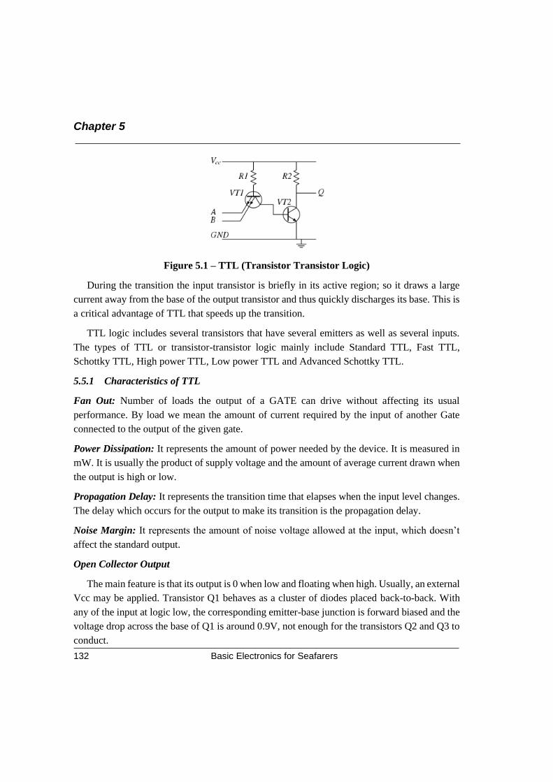
Chapter 5
Basic Electronics for Seafarers 132
Figure 5.1 – TTL (Transistor Transistor Logic)
During the transition the input transistor is briefly in its active region; so it draws a large
current away from the base of the output transistor and thus quickly discharges its base. This is
a critical advantage of TTL that speeds up the transition.
TTL logic includes several transistors that have several emitters as well as several inputs.
The types of TTL or transistor-transistor logic mainly include Standard TTL, Fast TTL,
Schottky TTL, High power TTL, Low power TTL and Advanced Schottky TTL.
5.5.1 Characteristics of TTL
Fan Out: Number of loads the output of a GATE can drive without affecting its usual
performance. By load we mean the amount of current required by the input of another Gate
connected to the output of the given gate.
Power Dissipation: It represents the amount of power needed by the device. It is measured in
mW. It is usually the product of supply voltage and the amount of average current drawn when
the output is high or low.
Propagation Delay: It represents the transition time that elapses when the input level changes.
The delay which occurs for the output to make its transition is the propagation delay.
Noise Margin: It represents the amount of noise voltage allowed at the input, which doesn’t
affect the standard output.
Open Collector Output
The main feature is that its output is 0 when low and floating when high. Usually, an external
Vcc may be applied. Transistor Q1 behaves as a cluster of diodes placed back-to-back. With
any of the input at logic low, the corresponding emitter-base junction is forward biased and the
voltage drop across the base of Q1 is around 0.9V, not enough for the transistors Q2 and Q3 to
conduct.
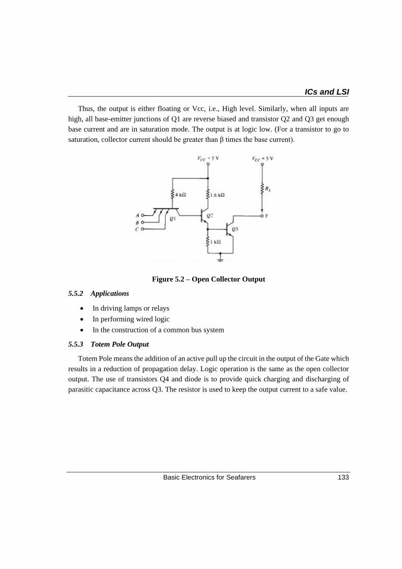
ICs and LSI
Basic Electronics for Seafarers 133
Thus, the output is either floating or Vcc, i.e., High level. Similarly, when all inputs are
high, all base-emitter junctions of Q1 are reverse biased and transistor Q2 and Q3 get enough
base current and are in saturation mode. The output is at logic low. (For a transistor to go to
saturation, collector current should be greater than β times the base current).
Figure 5.2 – Open Collector Output
5.5.2 Applications
• In driving lamps or relays
• In performing wired logic
• In the construction of a common bus system
5.5.3 Totem Pole Output
Totem Pole means the addition of an active pull up the circuit in the output of the Gate which
results in a reduction of propagation delay. Logic operation is the same as the open collector
output. The use of transistors Q4 and diode is to provide quick charging and discharging of
parasitic capacitance across Q3. The resistor is used to keep the output current to a safe value.
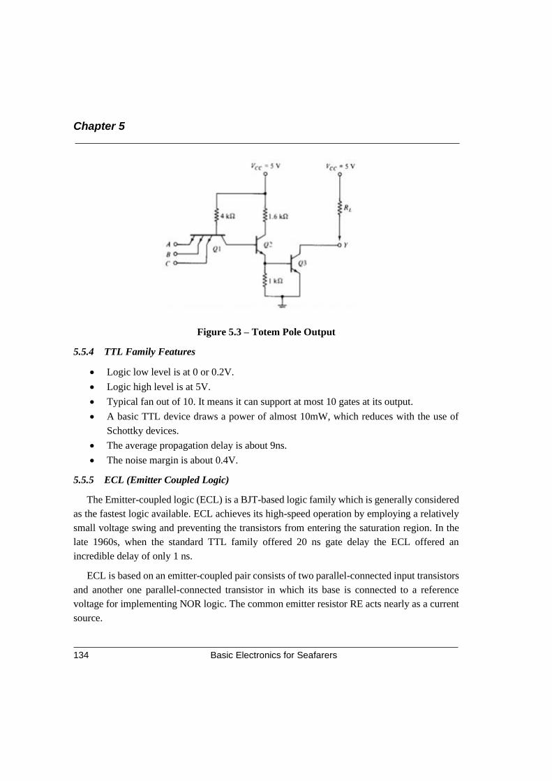
Chapter 5
Basic Electronics for Seafarers 134
Figure 5.3 – Totem Pole Output
5.5.4 TTL Family Features
• Logic low level is at 0 or 0.2V.
• Logic high level is at 5V.
• Typical fan out of 10. It means it can support at most 10 gates at its output.
• A basic TTL device draws a power of almost 10mW, which reduces with the use of
Schottky devices.
• The average propagation delay is about 9ns.
• The noise margin is about 0.4V.
5.5.5 ECL (Emitter Coupled Logic)
The Emitter-coupled logic (ECL) is a BJT-based logic family which is generally considered
as the fastest logic available. ECL achieves its high-speed operation by employing a relatively
small voltage swing and preventing the transistors from entering the saturation region. In the
late 1960s, when the standard TTL family offered 20 ns gate delay the ECL offered an
incredible delay of only 1 ns.
ECL is based on an emitter-coupled pair consists of two parallel-connected input transistors
and another one parallel-connected transistor in which its base is connected to a reference
voltage for implementing NOR logic. The common emitter resistor RE acts nearly as a current
source.
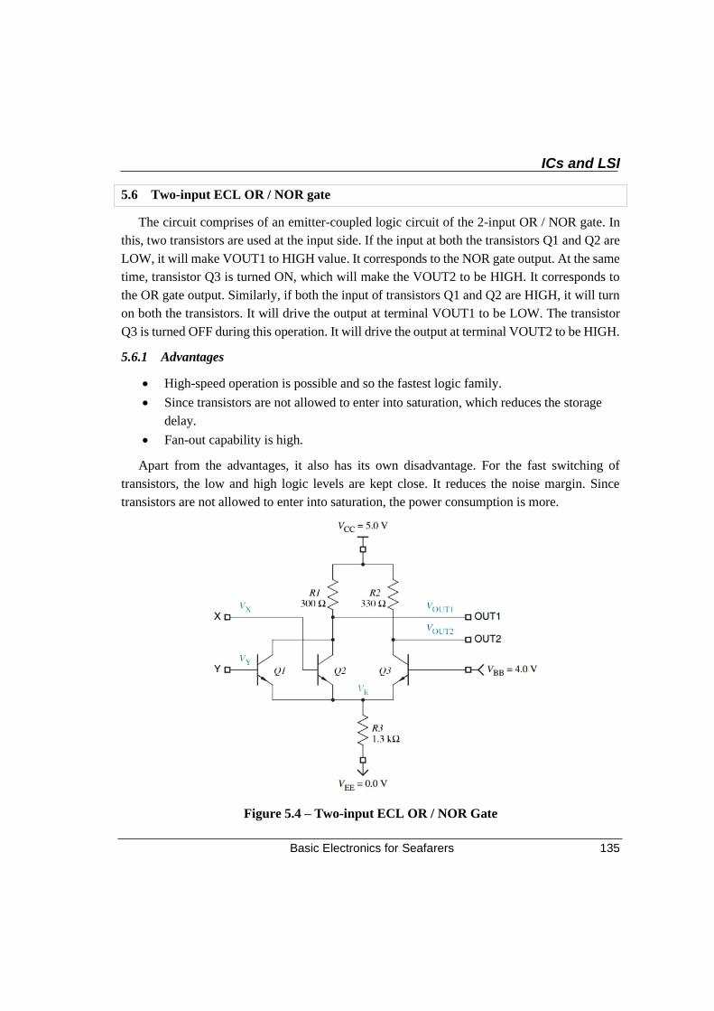
ICs and LSI
Basic Electronics for Seafarers 135
5.6 Two-input ECL OR / NOR gate
The circuit comprises of an emitter-coupled logic circuit of the 2-input OR / NOR gate. In
this, two transistors are used at the input side. If the input at both the transistors Q1 and Q2 are
LOW, it will make VOUT1 to HIGH value. It corresponds to the NOR gate output. At the same
time, transistor Q3 is turned ON, which will make the VOUT2 to be HIGH. It corresponds to
the OR gate output. Similarly, if both the input of transistors Q1 and Q2 are HIGH, it will turn
on both the transistors. It will drive the output at terminal VOUT1 to be LOW. The transistor
Q3 is turned OFF during this operation. It will drive the output at terminal VOUT2 to be HIGH.
5.6.1 Advantages
• High-speed operation is possible and so the fastest logic family.
• Since transistors are not allowed to enter into saturation, which reduces the storage
delay.
• Fan-out capability is high.
Apart from the advantages, it also has its own disadvantage. For the fast switching of
transistors, the low and high logic levels are kept close. It reduces the noise margin. Since
transistors are not allowed to enter into saturation, the power consumption is more.
Figure 5.4 – Two-input ECL OR / NOR Gate
Chapter 5
Basic Electronics for Seafarers 136
ECL circuits usually operate with negative power supplies (positive end of the supply is
connected to ground). Other logic families ground the negative end of the power supply. This
is done mainly to minimize the influence of the power supply variations on the logic levels.
ECL is more sensitive to noise on the VCC and is relatively immune to noise on VEE. Because
ground should be the most stable voltage in a system, ECL is specified with a positive ground.
5.7 TTL Comparison with ECL
Specification TTL ECL
Basic Gate NAND OR/NOR
Fan-out 10 25
Noise Immunity Strong Good
Clock Speed in MHz 35 >60
Power in mW 10 40-55
Propagation Delay in ns 10-30 1-2
Noise Margin Medium Low
5.8 Semiconductor Memories
A Memory is the portion of a system for storing data in large quantities. In semiconductor
memories latches or capacitors are used to store the data in binary form either a logical Zero or
a logical One. The smallest unit of binary data is a bit. The collection of 8 bits is called a byte
of data.
The data is stored as arrays and the one bit of data in it is called a cell. The location of each
cell is called an address. There are two major semiconductor memory categories RAM
(Random access memory) and ROM (Read only memory).
5.8.1 RAM (Random Access Memory)
In a RAM, all the addresses are accessible in an equal amount of time and can be selected
on any order for a read or write operation. All RAMs have both read and write capabilities.
RAM loose stored data when the power is turned off, so they are volatile memories. Flip-Flop
is an example for RAM.
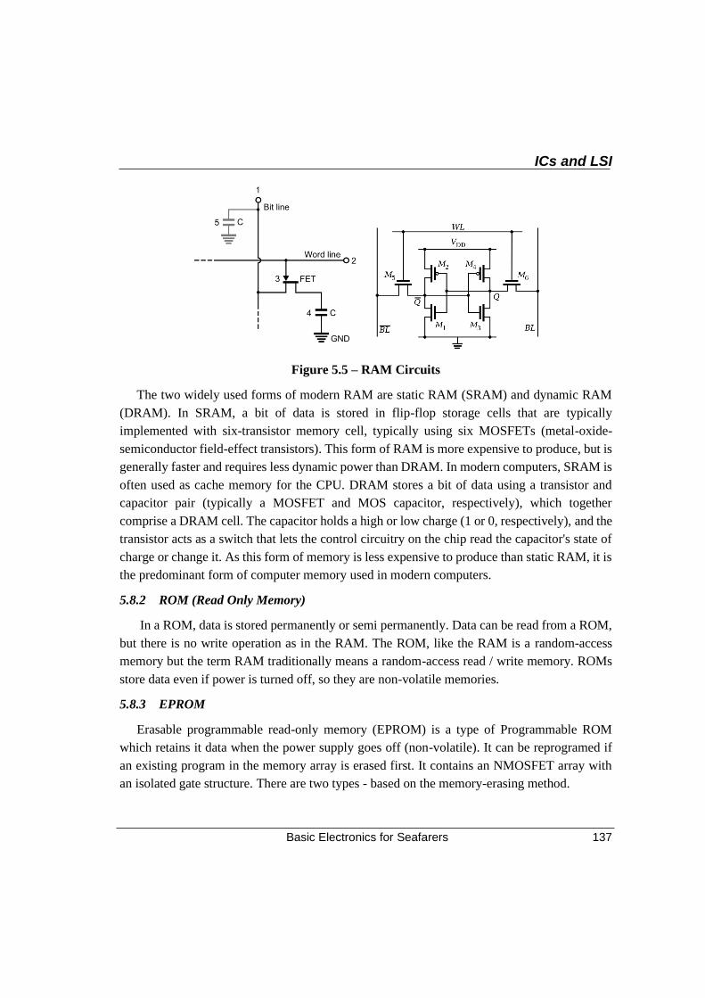
ICs and LSI
Basic Electronics for Seafarers 137
Figure 5.5 – RAM Circuits
The two widely used forms of modern RAM are static RAM (SRAM) and dynamic RAM
(DRAM). In SRAM, a bit of data is stored in flip-flop storage cells that are typically
implemented with six-transistor memory cell, typically using six MOSFETs (metal-oxide-
semiconductor field-effect transistors). This form of RAM is more expensive to produce, but is
generally faster and requires less dynamic power than DRAM. In modern computers, SRAM is
often used as cache memory for the CPU. DRAM stores a bit of data using a transistor and
capacitor pair (typically a MOSFET and MOS capacitor, respectively), which together
comprise a DRAM cell. The capacitor holds a high or low charge (1 or 0, respectively), and the
transistor acts as a switch that lets the control circuitry on the chip read the capacitor's state of
charge or change it. As this form of memory is less expensive to produce than static RAM, it is
the predominant form of computer memory used in modern computers.
5.8.2 ROM (Read Only Memory)
In a ROM, data is stored permanently or semi permanently. Data can be read from a ROM,
but there is no write operation as in the RAM. The ROM, like the RAM is a random-access
memory but the term RAM traditionally means a random-access read / write memory. ROMs
store data even if power is turned off, so they are non-volatile memories.
5.8.3 EPROM
Erasable programmable read-only memory (EPROM) is a type of Programmable ROM
which retains it data when the power supply goes off (non-volatile). It can be reprogramed if
an existing program in the memory array is erased first. It contains an NMOSFET array with
an isolated gate structure. There are two types - based on the memory-erasing method.
Chapter 5
Basic Electronics for Seafarers 138
First there is the UVEPROM, here erase can be done by exposure of the mercury array chip
to a high intensity UV radiation through quartz window on top of the package. It can be easily
recognizable by the transparent fused quartz window on the top of the package, through which
the silicon chip is visible. The erasing window must be kept covered with an opaque label to
prevent accidental erasure by the UV found in sunlight or camera flashes.
The second one is the EEPROM, it is electrically erasable programmable ROM. It can be
both programed and erased by using electrical pulses. It is available in floating gate type MOS
and Metal nitride-oxide silicone (MNOS) types.
5.8.4 CMOS Memory
Complementary metal–oxide–semiconductor (CMOS), is a type of metal–oxide–
semiconductor field-effect transistor (MOSFET) fabrication process that uses complementary
and symmetrical pairs of p-type and n-type MOSFETs for logic functions. CMOS technology
is used for constructing integrated circuit (IC) chips, including microprocessors,
microcontrollers, memory chips (including CMOS BIOS), and other digital logic circuits.
CMOS technology is also used for analog circuits such as image sensors (CMOS sensors), data
converters, RF circuits (RF CMOS), and highly integrated transceivers for many types of
communication.
CMOS memory is the area of memory which is sort of semi-permanent. . CMOS holds data
very well with minimal power (by the use of a low voltage battery), meaning that it can retain
important system configuration data for a device even when it is powered off. Unlike ROM
however, CMOS can be updated and changed through the use of plug and play devices. It stores
things such as the amount of memory installed, the date and time for the system, the number
and size of the hard drives that are installed and the clock.
5.9 Central Processing Unit (CPU)
A central processing unit (CPU) is an electronic circuitry that executes instructions
comprising a computer program. The CPU performs basic arithmetic, logic, controlling, and
input/output (I/O) operations specified by the instructions in the program. This contrasts with
external components such as main memory and I/O circuitry, and specialized processors such
as graphics processing units (GPUs).
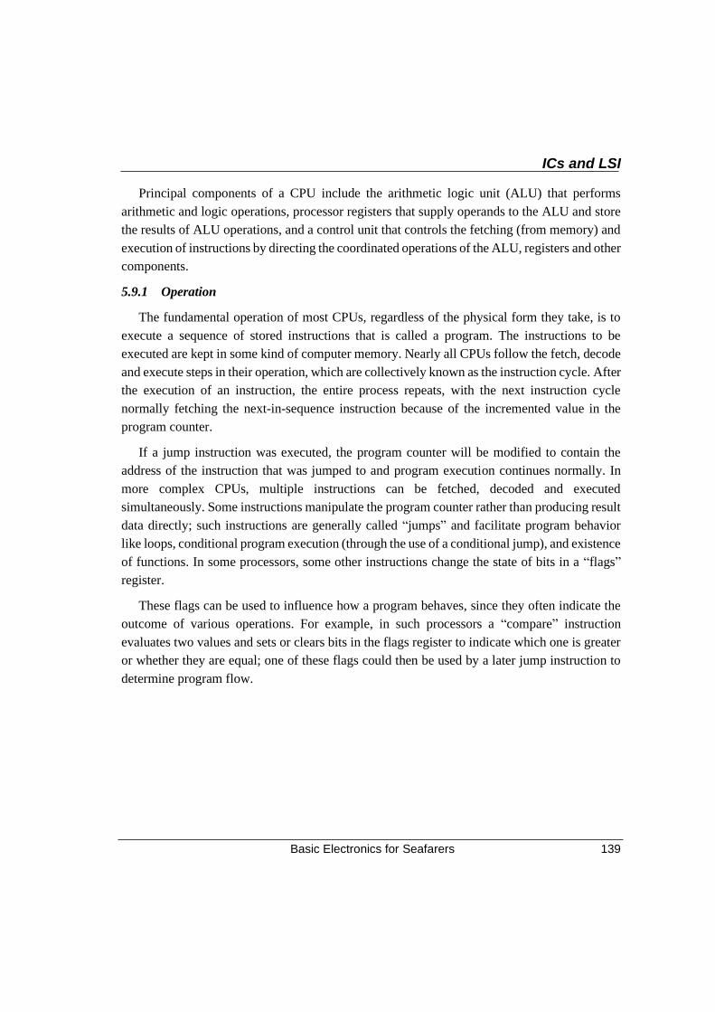
ICs and LSI
Basic Electronics for Seafarers 139
Principal components of a CPU include the arithmetic logic unit (ALU) that performs
arithmetic and logic operations, processor registers that supply operands to the ALU and store
the results of ALU operations, and a control unit that controls the fetching (from memory) and
execution of instructions by directing the coordinated operations of the ALU, registers and other
components.
5.9.1 Operation
The fundamental operation of most CPUs, regardless of the physical form they take, is to
execute a sequence of stored instructions that is called a program. The instructions to be
executed are kept in some kind of computer memory. Nearly all CPUs follow the fetch, decode
and execute steps in their operation, which are collectively known as the instruction cycle. After
the execution of an instruction, the entire process repeats, with the next instruction cycle
normally fetching the next-in-sequence instruction because of the incremented value in the
program counter.
If a jump instruction was executed, the program counter will be modified to contain the
address of the instruction that was jumped to and program execution continues normally. In
more complex CPUs, multiple instructions can be fetched, decoded and executed
simultaneously. Some instructions manipulate the program counter rather than producing result
data directly; such instructions are generally called “jumps” and facilitate program behavior
like loops, conditional program execution (through the use of a conditional jump), and existence
of functions. In some processors, some other instructions change the state of bits in a “flags”
register.
These flags can be used to influence how a program behaves, since they often indicate the
outcome of various operations. For example, in such processors a “compare” instruction
evaluates two values and sets or clears bits in the flags register to indicate which one is greater
or whether they are equal; one of these flags could then be used by a later jump instruction to
determine program flow.
Chapter 5
Basic Electronics for Seafarers 140
Figure 5.6 – A Block Diagram of A CPU
5.9.2 Fetch
The first step, fetch, involves taking an instruction from program memory. The instruction's
location (address) in program memory is determined by the program counter (PC) which stores
a number that identifies the address of the next instruction to be fetched.
After an instruction is fetched, the PC is incremented by the length of the instruction so that
it will contain the address of the next instruction in the sequence.
5.9.3 Decode
The instruction that the CPU fetches from memory determines what the CPU will do. In the
decode step, performed by the circuitry known as the instruction decoder, the instruction is
converted into signals that control other parts of the CPU.
ICs and LSI
Basic Electronics for Seafarers 141
One group of bits (“field”) within the instruction, called the opcode, indicates which
operation is to be performed, while the remaining fields usually provide supplemental
information required for the operation, such as the operands. Those operands may be specified
as a constant value (called an immediate value), or as the location of a value that may be a
processor register or a memory address, as determined by some addressing mode.
5.9.4 Execute
After the fetch and decode steps, the execute step is performed. Depending on the CPU
architecture, this may consist of a single action or a sequence of actions. During each action,
various parts of the CPU are electrically connected so they can perform all or part of the desired
operation and then the action is completed, typically in response to a clock pulse.
Very often the results are written to an internal CPU register for quick access by subsequent
instructions. In other cases, results may be written to slower, but less expensive and higher
capacity main memory.
For example, if an addition instruction is to be executed, the arithmetic logic unit (ALU)
inputs are connected to a pair of operand sources (numbers to be summed), the ALU is
configured to perform an addition operation so that the sum of its operand inputs will appear at
its output, and the ALU output is connected to storage (e.g., a register or memory) that will
receive the sum.
When the clock pulse occurs, the sum will be transferred to storage and, if the resulting sum
is too large (i.e., it is larger than the ALU's output word size), an arithmetic overflow flag will
be set.

Chapter 5
Basic Electronics for Seafarers 142
Sources
• www.daenotes.com/
• www.elprocus.com/
• www.wikipedia.org/
• http://wakerly.org/DDPP/DDPP4student/Supplementary_sections/ECL.pdf
I hope that I was able to make you
understand the basics of the IC and
LSI techniques and all the other
topics that I mentioned above. Also,
now you can co-relate the
applications of these topics with
your so called “cool electronic
gadgets”
WOOOOOHHHOOOOOOO!! These
topics were so interesting Sir! I was
able to grasp them very well. All
these diagrams were so self
explanatory. Also, as you said sir.
“Going back to basics strengthens
your foundation”. And so, it did to me!

Chapter 6 Digital Techniques
Basic Electronics for Seafarers
Sir, I was waiting for this chapter for
a while. Frankly speaking whenever I
think of electronics. The first picture
that comes in my mind is of those
triangular logic gates and truth tables.
LOL!!!!
It’s literally fun to solve all those logic
circuits.
Yes Divyam, well said!
These logic gates are very
important in the study of
digital electronics. But our
aim is not only to solve
those logic gate diagrams
and memorise truth tables.
More than that, you should
know the application of it.
Also, a good understading
of digital electronics is a
must!!
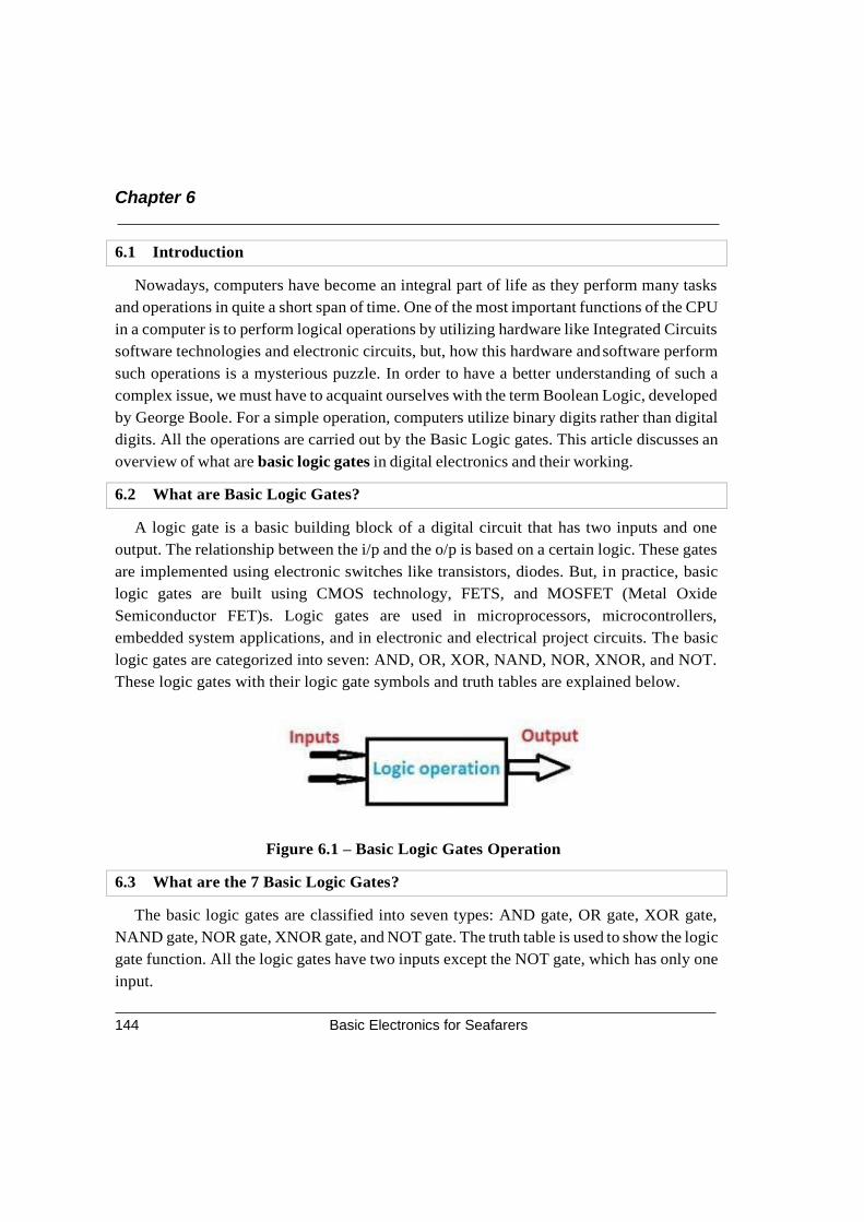
Chapter 6
Basic Electronics for Seafarers 144
6.1 Introduction
Nowadays, computers have become an integral part of life as they perform many tasks
and operations in quite a short span of time. One of the most important functions of the CPU
in a computer is to perform logical operations by utilizing hardware like Integrated Circuits
software technologies and electronic circuits, but, how this hardware and software perform
such operations is a mysterious puzzle. In order to have a better understanding of such a
complex issue, we must have to acquaint ourselves with the term Boolean Logic, developed
by George Boole. For a simple operation, computers utilize binary digits rather than digital
digits. All the operations are carried out by the Basic Logic gates. This article discusses an
overview of what are basic logic gates in digital electronics and their working.
6.2 What are Basic Logic Gates?
A logic gate is a basic building block of a digital circuit that has two inputs and one
output. The relationship between the i/p and the o/p is based on a certain logic. These gates
are implemented using electronic switches like transistors, diodes. But, in practice, basic
logic gates are built using CMOS technology, FETS, and MOSFET (Metal Oxide
Semiconductor FET)s. Logic gates are used in microprocessors, microcontrollers,
embedded system applications, and in electronic and electrical project circuits. The basic
logic gates are categorized into seven: AND, OR, XOR, NAND, NOR, XNOR, and NOT.
These logic gates with their logic gate symbols and truth tables are explained below.
Figure 6.1 – Basic Logic Gates Operation
6.3 What are the 7 Basic Logic Gates?
The basic logic gates are classified into seven types: AND gate, OR gate, XOR gate,
NAND gate, NOR gate, XNOR gate, and NOT gate. The truth table is used to show the logic
gate function. All the logic gates have two inputs except the NOT gate, which has only one
input.
Digital Techniques
Basic Electronics for Seafarers 145
When drawing a truth table, the binary values 0 and 1 are used. Every possible
combination depends on the number of inputs. If you don’t know about the logic gates and
their truth tables and need guidance on them, please go through the following infographic
that gives an overview of logic gates with their symbols and truth tables.
6.4 Why we use Basic Logic Gates?
The basic logic gates are used to perform fundamental logical functions. These are the
basic building blocks in the digital ICs (integrated circuits). Most of the logic gates use two
binary inputs and generates a single output like 1 or 0. In some electronic circuits, few logic
gates are used whereas in some other circuits, microprocessors include millions of logic
gates.
The implementation of Logic gates can be done through diodes, transistors, relays,
molecules, and optics otherwise different mechanical elements. Because of this reason,
basic logic gates are used like electronic circuits.
6.4.1 Binary and Decimal
Before talking about the truth tables of logic gates, it is essential to know the background
of binary and decimal numbers. We all know the decimal numbers which we utilize in
everyday calculations like 0 to 9. This kind of number system includes the base-
In the same way, binary numbers like 0 and 1 can be utilized to signify decimal numbers
wherever the base of the binary numbers is 2.
The significance of using binary numbers here is to signify the switching position
otherwise voltage position of a digital component. Here 1 represents the High signal or high
voltage whereas “0” specifies low voltage or low signal. Therefore, Boolean algebra was
started. After that, each logic gate is discussed separately this contains the logic of the gate,
truth table, and its typical symbol.
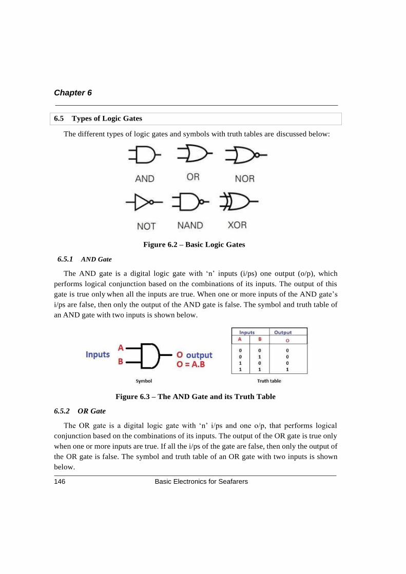
Chapter 6
Basic Electronics for Seafarers 146
6.5 Types of Logic Gates
The different types of logic gates and symbols with truth tables are discussed below:
Figure 6.2 – Basic Logic Gates
6.5.1 AND Gate
The AND gate is a digital logic gate with ‘n’ inputs (i/ps) one output (o/p), which
performs logical conjunction based on the combinations of its inputs. The output of this
gate is true only when all the inputs are true. When one or more inputs of the AND gate’s
i/ps are false, then only the output of the AND gate is false. The symbol and truth table of
an AND gate with two inputs is shown below.
Figure 6.3 – The AND Gate and its Truth Table
6.5.2 OR Gate
The OR gate is a digital logic gate with ‘n’ i/ps and one o/p, that performs logical
conjunction based on the combinations of its inputs. The output of the OR gate is true only
when one or more inputs are true. If all the i/ps of the gate are false, then only the output of
the OR gate is false. The symbol and truth table of an OR gate with two inputs is shown
below.
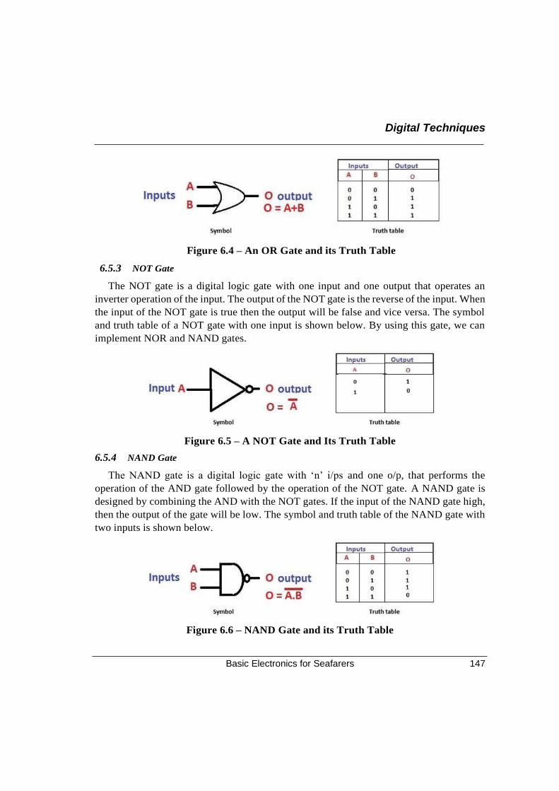
Digital Techniques
Basic Electronics for Seafarers 147
Figure 6.4 – An OR Gate and its Truth Table
6.5.3 NOT Gate
The NOT gate is a digital logic gate with one input and one output that operates an
inverter operation of the input. The output of the NOT gate is the reverse of the input. When
the input of the NOT gate is true then the output will be false and vice versa. The symbol
and truth table of a NOT gate with one input is shown below. By using this gate, we can
implement NOR and NAND gates.
Figure 6.5 – A NOT Gate and Its Truth Table
6.5.4 NAND Gate
The NAND gate is a digital logic gate with ‘n’ i/ps and one o/p, that performs the
operation of the AND gate followed by the operation of the NOT gate. A NAND gate is
designed by combining the AND with the NOT gates. If the input of the NAND gate high,
then the output of the gate will be low. The symbol and truth table of the NAND gate with
two inputs is shown below.
Figure 6.6 – NAND Gate and its Truth Table
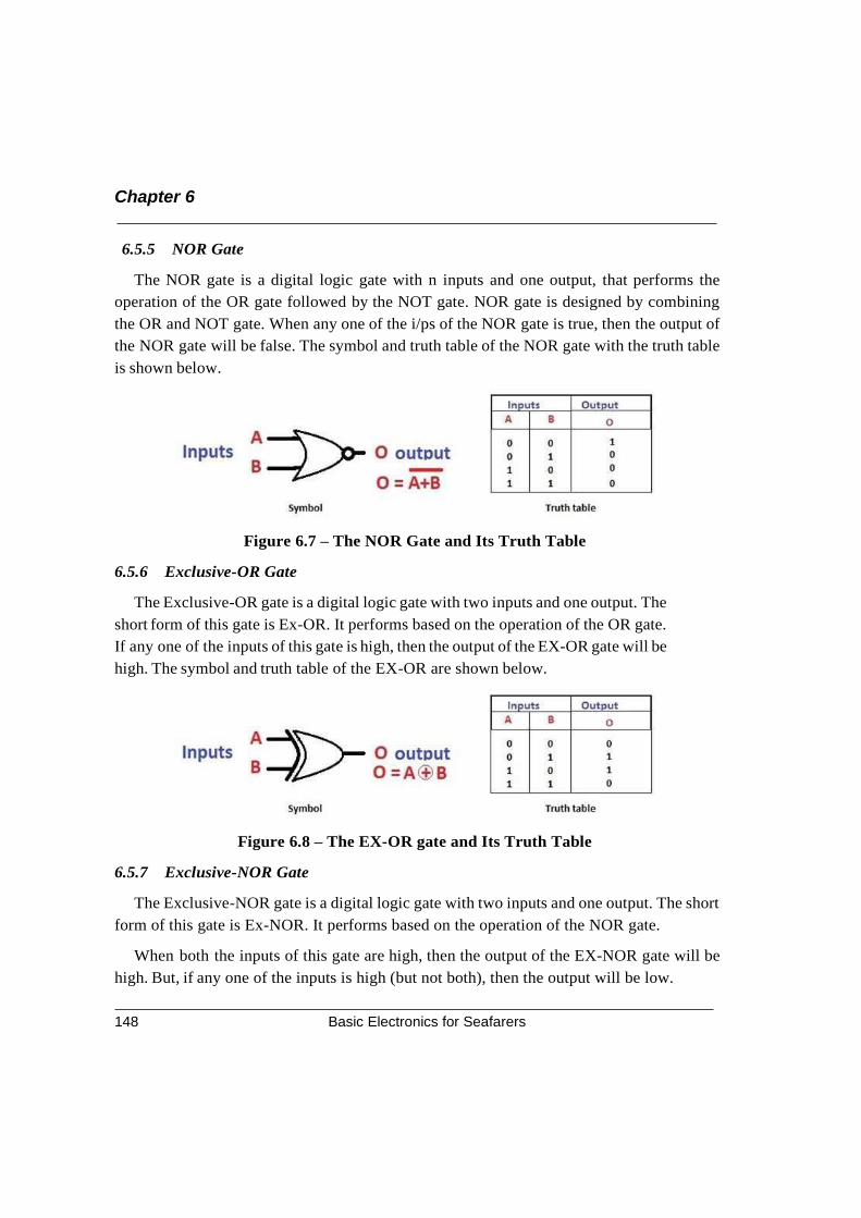
Chapter 6
Basic Electronics for Seafarers 148
6.5.5 NOR Gate
The NOR gate is a digital logic gate with n inputs and one output, that performs the
operation of the OR gate followed by the NOT gate. NOR gate is designed by combining
the OR and NOT gate. When any one of the i/ps of the NOR gate is true, then the output of
the NOR gate will be false. The symbol and truth table of the NOR gate with the truth table
is shown below.
Figure 6.7 – The NOR Gate and Its Truth Table
6.5.6 Exclusive-OR Gate
The Exclusive-OR gate is a digital logic gate with two inputs and one output. The
short form of this gate is Ex-OR. It performs based on the operation of the OR gate.
If any one of the inputs of this gate is high, then the output of the EX-OR gate will be
high. The symbol and truth table of the EX-OR are shown below.
Figure 6.8 – The EX-OR gate and Its Truth Table
6.5.7 Exclusive-NOR Gate
The Exclusive-NOR gate is a digital logic gate with two inputs and one output. The short
form of this gate is Ex-NOR. It performs based on the operation of the NOR gate.
When both the inputs of this gate are high, then the output of the EX-NOR gate will be
high. But, if any one of the inputs is high (but not both), then the output will be low.
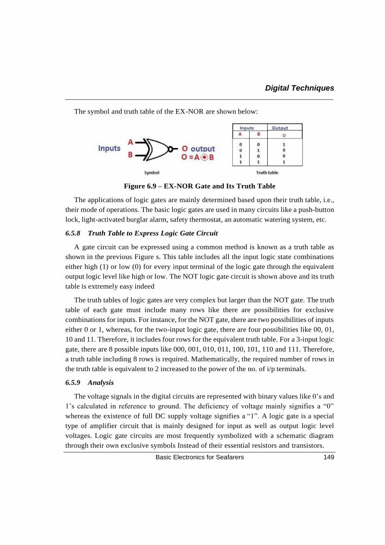
Digital Techniques
Basic Electronics for Seafarers 149
The symbol and truth table of the EX-NOR are shown below:
Figure 6.9 – EX-NOR Gate and Its Truth Table
The applications of logic gates are mainly determined based upon their truth table, i.e.,
their mode of operations. The basic logic gates are used in many circuits like a push-button
lock, light-activated burglar alarm, safety thermostat, an automatic watering system, etc.
6.5.8 Truth Table to Express Logic Gate Circuit
A gate circuit can be expressed using a common method is known as a truth table as
shown in the previous Figure s. This table includes all the input logic state combinations
either high (1) or low (0) for every input terminal of the logic gate through the equivalent
output logic level like high or low. The NOT logic gate circuit is shown above and its truth
table is extremely easy indeed
The truth tables of logic gates are very complex but larger than the NOT gate. The truth
table of each gate must include many rows like there are possibilities for exclusive
combinations for inputs. For instance, for the NOT gate, there are two possibilities of inputs
either 0 or 1, whereas, for the two-input logic gate, there are four possibilities like 00, 01,
10 and 11. Therefore, it includes four rows for the equivalent truth table. For a 3-input logic
gate, there are 8 possible inputs like 000, 001, 010, 011, 100, 101, 110 and 111. Therefore,
a truth table including 8 rows is required. Mathematically, the required number of rows in
the truth table is equivalent to 2 increased to the power of the no. of i/p terminals.
6.5.9 Analysis
The voltage signals in the digital circuits are represented with binary values like 0’s and
1’s calculated in reference to ground. The deficiency of voltage mainly signifies a “0”
whereas the existence of full DC supply voltage signifies a “1”. A logic gate is a special
type of amplifier circuit that is mainly designed for input as well as output logic level
voltages. Logic gate circuits are most frequently symbolized with a schematic diagram
through their own exclusive symbols Instead of their essential resistors and transistors.
Chapter 6
Basic Electronics for Seafarers 150
Just like with Op-Amps (operational amplifiers), the connections of power supply to
logic gates are frequently misplaced in schematic diagrams for the benefit of simplicity. It
includes the probable input logic level combinations through their particular output logic
levels.
The easiest way to learn the function of basic logic gates is explained below:
• For AND Gate – If both the inputs are high then the output is also high
• For OR Gate – If a minimum of one input is high then the output is High
• For XOR Gate – If the minimum one input is high then only the output is high
• NAND Gate – If the minimum one input is low then the output is high
• NOR Gate – If both the inputs are low then the output is high.
6.6 De Morgan’s Theorem
The first theorem of DeMorgan states that the logic gate like NAND is equal to an OR
gate with a bubble. The logic function of the NAND gate is
A’B = A’+B’
The second theorem of DeMorgan states that the NOR logic gate is equal to an AND
gate with a bubble. The logic function of NOR gate is
(A+B)’= A’. B’
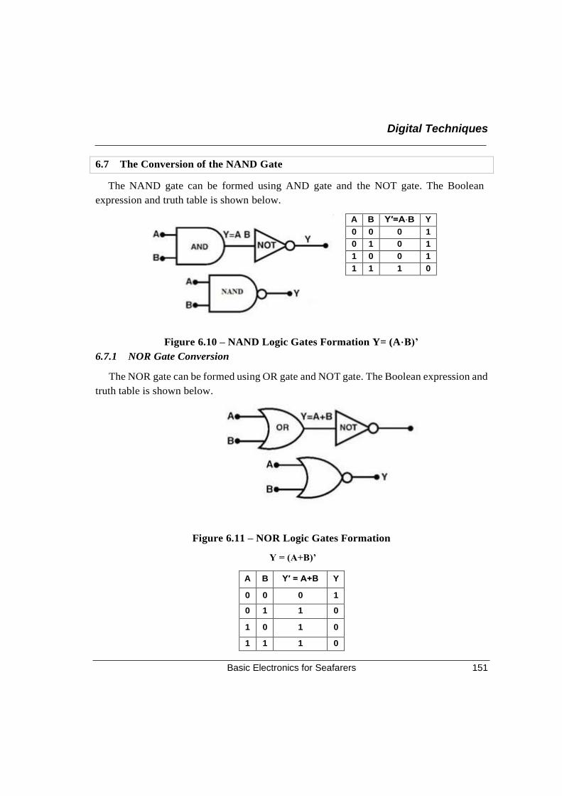
Digital Techniques
Basic Electronics for Seafarers 151
6.7 The Conversion of the NAND Gate
The NAND gate can be formed using AND gate and the NOT gate. The Boolean
expression and truth table is shown below.
A B Y′=A⋅B Y
0 0 0 1
0 1 0 1
1 0 0 1
1 1 1 0
Figure 6.10 – NAND Logic Gates Formation Y= (A⋅B)’
6.7.1 NOR Gate Conversion
The NOR gate can be formed using OR gate and NOT gate. The Boolean expression and
truth table is shown below.
Figure 6.11 – NOR Logic Gates Formation
Y = (A+B)’
A B Y′ = A+B Y
0 0 0 1
0 1 1 0
1 0 1 0
1 1 1 0
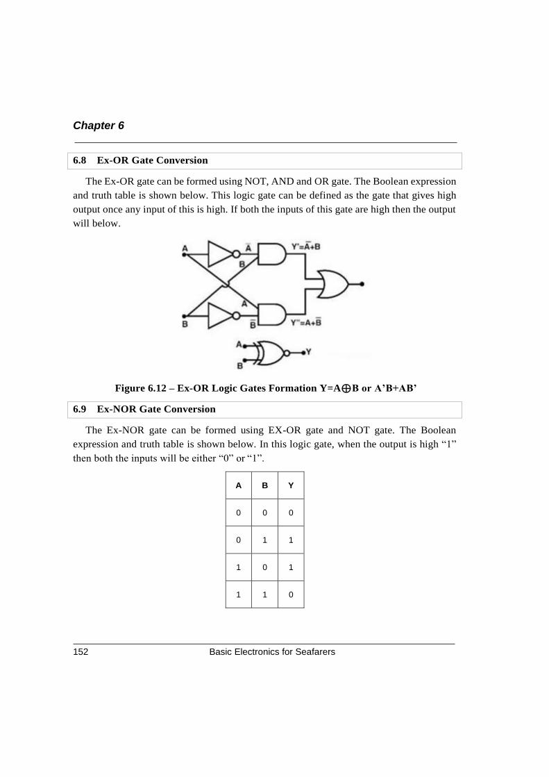
Chapter 6
Basic Electronics for Seafarers 152
6.8 Ex-OR Gate Conversion
The Ex-OR gate can be formed using NOT, AND and OR gate. The Boolean expression
and truth table is shown below. This logic gate can be defined as the gate that gives high
output once any input of this is high. If both the inputs of this gate are high then the output
will below.
Figure 6.12 – Ex-OR Logic Gates Formation Y=A⊕B or A’B+AB’
6.9 Ex-NOR Gate Conversion
The Ex-NOR gate can be formed using EX-OR gate and NOT gate. The Boolean
expression and truth table is shown below. In this logic gate, when the output is high “1”
then both the inputs will be either “0” or “1”.
A B Y
0 0 0
0 1 1
1 0 1
1 1 0
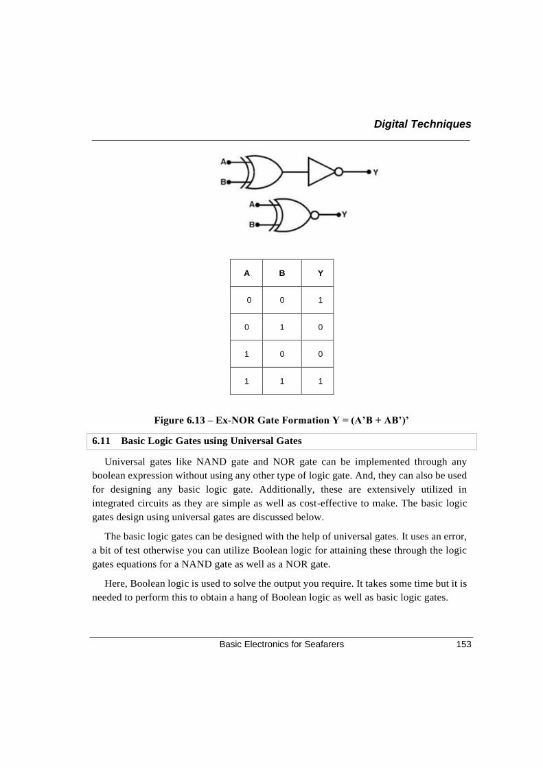
Digital Techniques
Basic Electronics for Seafarers 153
A B Y
0 0 1
0 1 0
1 0 0
1 1 1
Figure 6.13 – Ex-NOR Gate Formation Y = (A’B + AB’)’
6.11 Basic Logic Gates using Universal Gates
Universal gates like NAND gate and NOR gate can be implemented through any
boolean expression without using any other type of logic gate. And, they can also be used
for designing any basic logic gate. Additionally, these are extensively utilized in
integrated circuits as they are simple as well as cost-effective to make. The basic logic
gates design using universal gates are discussed below.
The basic logic gates can be designed with the help of universal gates. It uses an error,
a bit of test otherwise you can utilize Boolean logic for attaining these through the logic
gates equations for a NAND gate as well as a NOR gate.
Here, Boolean logic is used to solve the output you require. It takes some time but it is
needed to perform this to obtain a hang of Boolean logic as well as basic logic gates.
Chapter 6
Basic Electronics for Seafarers 154
6.11.1 Basic Logic Gates Using NAND Gate
The designing of basic logic gates using NAND gate is discussed below.
6.11.1.1 NOT Gate Design using NAND
The designing of the NOT gate is very simple by simply connecting both the inputs as one.
6.11.1.2 AND Gate Design using NAND
The designing of AND gate using NAND gate can be done at the NAND gate’s output to
reverse it and obtain AND logic.
6.11.1.3 OR Gate Design using NAND
The designing of OR gate using NAND gate can be done by connecting two NOT gates
using NAND gates at the NAND’s inputs to obtain OR logic.
6.11.1.4 NOR Gate Design using NAND
The designing of NOR gate using NAND gate can be done by simply connecting another
NOT gate through NAND gate to the o/p of an OR gate through NAND. EXOR Gate Design
using NAND
This one’s a bit tricky. You share the two inputs with three gates. The output of the first
NAND is the second input to the other two. Finally, another NAND takes the outputs of these
two NAND gates to give the final output.
6.11.2 Basic Logic Gates using NOR Gate
The designing of basic logic gates using NOR gate is discussed below.
6.11.2.1 NOT Gate using NOR
The designing of NOT gate with NOR gate is simple by connecting both the inputs as one.
6.11.2.2 OR Gate using NOR
The designing of OR Gate with NOR gate is simple by connecting at the o/p of the NOR
gate to reverse it and obtain OR logic.
6.11.2.3 AND Gate using NOR
The designing of AND gate using NOR gate can be done by connecting two NOT with
NOR gates at the NOR inputs to obtain AND logic.
Digital Techniques
Basic Electronics for Seafarers 155
6.11.2.4 NAND Gate using NOR
The designing of NAND Gate using NOR gate can be done by simply connecting another
NOT gate through NOR gate to the AND gate’s output with NOR.
6.11.2.5 EX-NOR Gate using NOR
This type of connection is a bit difficult because the two inputs can be shared with three
logic gates. The first NOR gate output is the next input to the remaining two gates. Finally,
another NOR gate uses the two NOR gate outputs to provide the last output.
6.11.2.6 Applications
The applications of basic logic gates are so many however they mostly depend on their
truth tables otherwise form of operations. Basic logic gates are frequently used in circuits like
a lock with push-button, the watering system automatically, burglar alarm activated through
light, safety thermostat and other types of electronic devices.
The main advantage of basic logic gates is, these can be used in a different combination
circuit. In addition, there is no boundary to the number of logic gates that can be utilized in a
single electronic device. But it can be limited because of the specified physical gap within the
device. In digital ICs (integrated circuits) we will discover a collection of the logic gate region
unit.
By using mixtures of basic logic gates, advanced operations are often performed. In theory,
there’s no limit to the number of gates that may be clad along during a single device. However,
in the application, there’s a limit to the number of gates that may be packed into a given
physical area. Arrays of the logic gate area unit are found in digital integrated circuits (ICs).
As IC technology advances, the desired physical volume for every individual gate
decrease, and digital devices of an equivalent or smaller size become capable of acting with
more complicated operations at ever-increasing speeds.
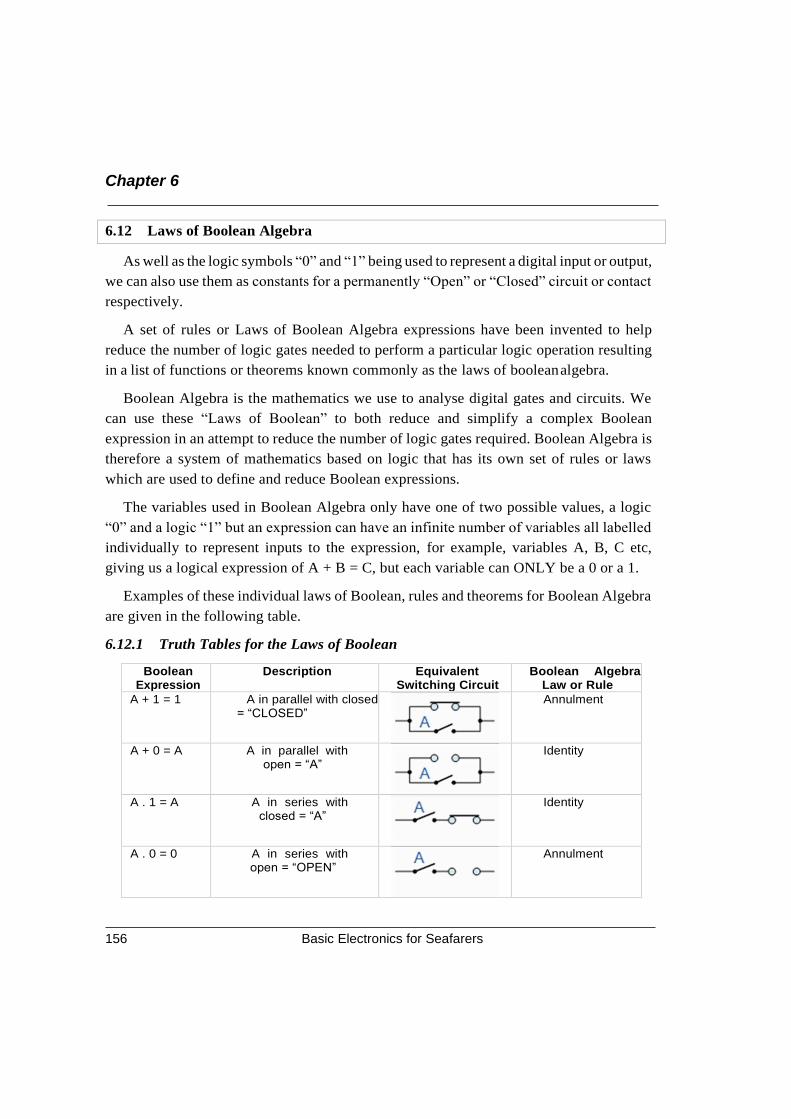
Chapter 6
Basic Electronics for Seafarers 156
6.12 Laws of Boolean Algebra
As well as the logic symbols “0” and “1” being used to represent a digital input or output,
we can also use them as constants for a permanently “Open” or “Closed” circuit or contact
respectively.
A set of rules or Laws of Boolean Algebra expressions have been invented to help
reduce the number of logic gates needed to perform a particular logic operation resulting
in a list of functions or theorems known commonly as the laws of boolean algebra.
Boolean Algebra is the mathematics we use to analyse digital gates and circuits. We
can use these “Laws of Boolean” to both reduce and simplify a complex Boolean
expression in an attempt to reduce the number of logic gates required. Boolean Algebra is
therefore a system of mathematics based on logic that has its own set of rules or laws
which are used to define and reduce Boolean expressions.
The variables used in Boolean Algebra only have one of two possible values, a logic
“0” and a logic “1” but an expression can have an infinite number of variables all labelled
individually to represent inputs to the expression, for example, variables A, B, C etc,
giving us a logical expression of A + B = C, but each variable can ONLY be a 0 or a 1.
Examples of these individual laws of Boolean, rules and theorems for Boolean Algebra
are given in the following table.
6.12.1 Truth Tables for the Laws of Boolean
Boolean Expression
Description Equivalent Switching Circuit
Boolean Algebra Law or Rule
A + 1 = 1 A in parallel with closed = “CLOSED”
Annulment
A + 0 = A A in parallel with open = “A”
Identity
A . 1 = A A in series with closed = “A”
Identity
A . 0 = 0 A in series with open = “OPEN”
Annulment
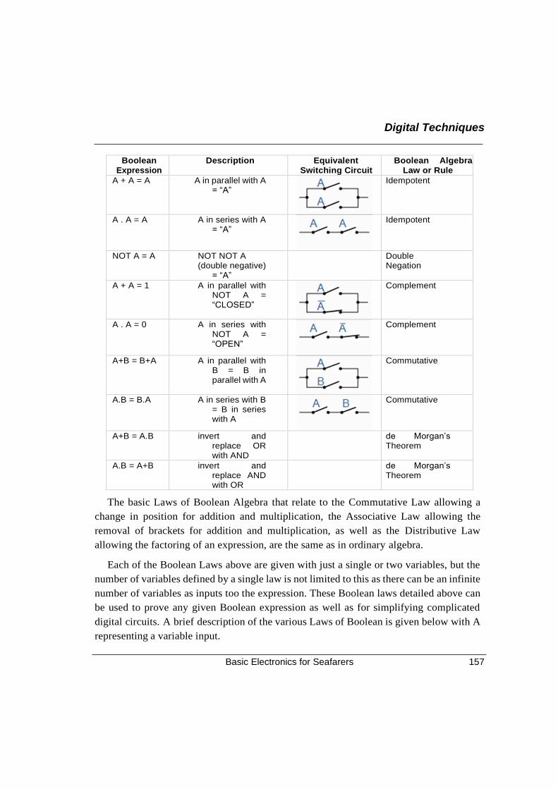
Digital Techniques
Basic Electronics for Seafarers 157
Boolean Expression
Description Equivalent Switching Circuit
Boolean Algebra Law or Rule
A + A = A A in parallel with A = “A”
Idempotent
A . A = A A in series with A = “A”
Idempotent
NOT A = A NOT NOT A (double negative)
= “A”
Double Negation
A + A = 1 A in parallel with NOT A = “CLOSED”
Complement
A . A = 0 A in series with NOT A = “OPEN”
Complement
A+B = B+A A in parallel with B = B in parallel with A
Commutative
A.B = B.A A in series with B = B in series with A
Commutative
A+B = A.B invert and replace OR with AND
de Morgan’s Theorem
A.B = A+B invert and replace AND with OR
de Morgan’s Theorem
The basic Laws of Boolean Algebra that relate to the Commutative Law allowing a
change in position for addition and multiplication, the Associative Law allowing the
removal of brackets for addition and multiplication, as well as the Distributive Law
allowing the factoring of an expression, are the same as in ordinary algebra.
Each of the Boolean Laws above are given with just a single or two variables, but the
number of variables defined by a single law is not limited to this as there can be an infinite
number of variables as inputs too the expression. These Boolean laws detailed above can
be used to prove any given Boolean expression as well as for simplifying complicated
digital circuits. A brief description of the various Laws of Boolean is given below with A
representing a variable input.
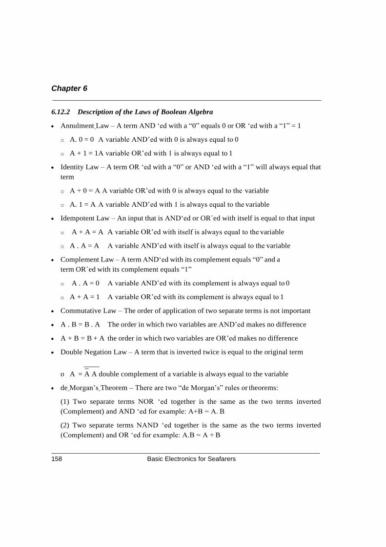
Chapter 6
Basic Electronics for Seafarers 158
6.12.2 Description of the Laws of Boolean Algebra
• Annulment Law – A term AND ‘ed with a “0” equals 0 or OR ‘ed with a “1” = 1
o A. 0 = 0 A variable AND’ed with 0 is always equal to 0
o A + 1 = 1A variable OR’ed with 1 is always equal to 1
• Identity Law – A term OR ‘ed with a “0” or AND ‘ed with a “1” will always equal that
term
o A + 0 = A A variable OR’ed with 0 is always equal to the variable
o A. 1 = A A variable AND’ed with 1 is always equal to the variable
• Idempotent Law – An input that is AND‘ed or OR´ed with itself is equal to that input
o A + A = A A variable OR’ed with itself is always equal to the variable
o A . A = A A variable AND’ed with itself is always equal to the variable
• Complement Law – A term AND‘ed with its complement equals “0” and a
term OR´ed with its complement equals “1”
o A . A = 0 A variable AND’ed with its complement is always equal to 0
o A + A = 1 A variable OR’ed with its complement is always equal to 1
• Commutative Law – The order of application of two separate terms is not important
• A . B = B . A The order in which two variables are AND’ed makes no difference
• A + B = B + A the order in which two variables are OR’ed makes no difference
• Double Negation Law – A term that is inverted twice is equal to the original term
_
o A = A A double complement of a variable is always equal to the variable
• de Morgan’s Theorem – There are two “de Morgan’s” rules or theorems:
(1) Two separate terms NOR ‘ed together is the same as the two terms inverted
(Complement) and AND ‘ed for example: A+B = A. B
(2) Two separate terms NAND ‘ed together is the same as the two terms inverted
(Complement) and OR ‘ed for example: A.B = A + B
Digital Techniques
Basic Electronics for Seafarers 159
Other algebraic Laws of Boolean not detailed above include:
• Boolean Postulates – While not Boolean Laws in their own right, these are a set of
Mathematical Laws which can be used in the simplification of Boolean Expressions.
o 0 . 0 = 0 A 0 AND’ed with itself is always equal to 0
o 1 . 1 = 1 A 1 AND’ed with itself is always equal to 1
o 1 . 0 = 0 A 1 AND’ed with a 0 is equal to 0
o 0 + 0 = 0 A 0 OR’ed with itself is always equal to 0
o 1 + 1 = 1 A 1 OR’ed with itself is always equal to 1
o 1 + 0 = 1 A 1 OR’ed with a 0 is equal to 1
o 1 = 0 The Inverse (Complement) of a 1 is always equal to 0
o 0 = 1 The Inverse (Complement) of a 0 is always equal to 1
• Distributive Law – This law permits the multiplying or factoring out of an expression.
• A(B + C) = A.B + A.C (OR Distributive Law)
• A + (B.C) = (A + B).(A + C) (AND Distributive Law)
• Absorptive Law – This law enables a reduction in a complicated
expression to a simpler one by absorbing like terms.
• A + (A.B) = (A.1) + (A.B) = A(1 + B) = A (OR Absorption Law)
• A(A + B) = (A + 0).(A + B) = A + (0.B) = A (AND Absorption Law)
• Associative Law – This law allows the removal of brackets from
an expression and regrouping of the variables.
• A + (B + C) = (A + B) + C = A + B + C (OR Associate Law)
• A(B.C) = (A.B)C = A . B . C (AND Associate Law)
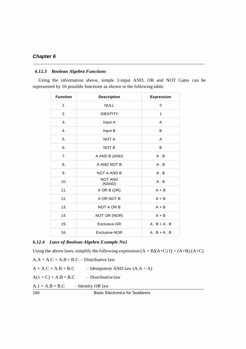
Chapter 6
Basic Electronics for Seafarers 160
6.12.3 Boolean Algebra Functions
Using the information above, simple 2-input AND, OR and NOT Gates can be
represented by 16 possible functions as shown in the following table:
Function Description Expression
1. NULL 0
2. IDENTITY 1
3. Input A A
4. Input B B
5. NOT A A
6. NOT B B
7. A AND B (AND) A . B
8. A AND NOT B A . B
9. NOT A AND B A . B
10. NOT AND (NAND)
A . B
11. A OR B (OR) A + B
12. A OR NOT B A + B
13. NOT A OR B A + B
14. NOT OR (NOR) A + B
15. Exclusive-OR A . B + A . B
16. Exclusive-NOR A . B + A . B
6.12.4 Laws of Boolean Algebra Example No1
Using the above laws, simplify the following expression:(A + B)(A+C) Q = (A+B).(A+C)
A.A + A.C + A.B + B.C – Distributive law
A + A.C + A.B + B.C – Idempotent AND law (A.A = A)
A(1 + C) + A.B + B.C – Distributive law
A.1 + A.B + B.C – Identity OR law
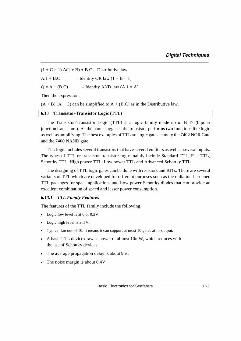
Digital Techniques
Basic Electronics for Seafarers 161
(1 + C = 1) A(1 + B) + B.C – Distributive law
A.1 + B.C – Identity OR law (1 + B = 1)
Q = A + (B.C) – Identity AND law (A.1 = A)
Then the expression:
(A + B) (A + C) can be simplified to A + (B.C) as in the Distributive law.
6.13 Transistor-Transistor Logic (TTL)
The Transistor-Transistor Logic (TTL) is a logic family made up of BJTs (bipolar
junction transistors). As the name suggests, the transistor performs two functions like logic
as well as amplifying. The best examples of TTL are logic gates namely the 7402 NOR Gate
and the 7400 NAND gate.
TTL logic includes several transistors that have several emitters as well as several inputs.
The types of TTL or transistor-transistor logic mainly include Standard TTL, Fast TTL,
Schottky TTL, High power TTL, Low power TTL and Advanced Schottky TTL.
The designing of TTL logic gates can be done with resistors and BJTs. There are several
variants of TTL which are developed for different purposes such as the radiation-hardened
TTL packages for space applications and Low power Schottky diodes that can provide an
excellent combination of speed and lesser power consumption.
6.13.1 TTL Family Features
The features of the TTL family include the following.
• Logic low level is at 0 or 0.2V.
• Logic high level is at 5V.
• Typical fan out of 10. It means it can support at most 10 gates at its output.
• A basic TTL device draws a power of almost 10mW, which reduces with
the use of Schottky devices.
• The average propagation delay is about 9ns.
• The noise margin is about 0.4V
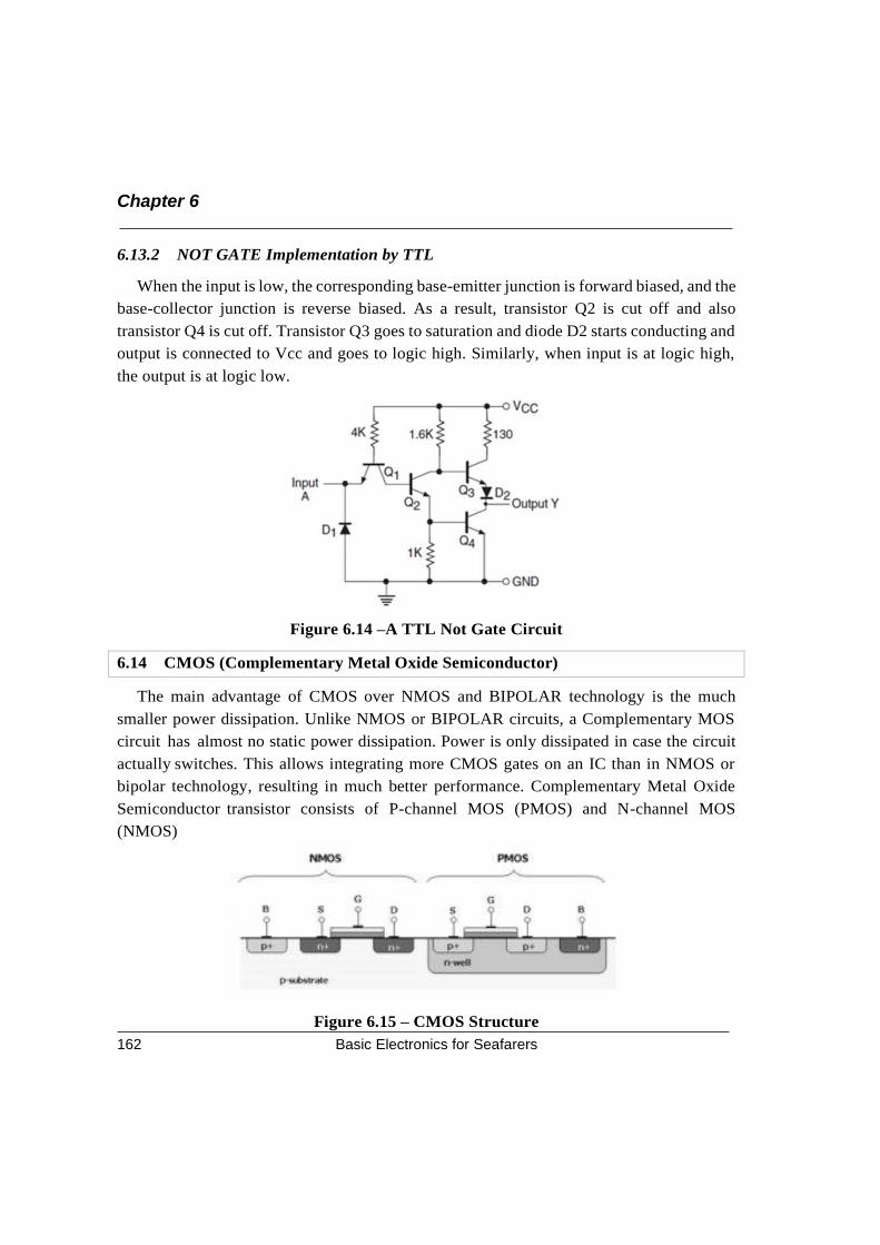
Chapter 6
Basic Electronics for Seafarers 162
6.13.2 NOT GATE Implementation by TTL
When the input is low, the corresponding base-emitter junction is forward biased, and the
base-collector junction is reverse biased. As a result, transistor Q2 is cut off and also
transistor Q4 is cut off. Transistor Q3 goes to saturation and diode D2 starts conducting and
output is connected to Vcc and goes to logic high. Similarly, when input is at logic high,
the output is at logic low.
Figure 6.14 –A TTL Not Gate Circuit
6.14 CMOS (Complementary Metal Oxide Semiconductor)
The main advantage of CMOS over NMOS and BIPOLAR technology is the much
smaller power dissipation. Unlike NMOS or BIPOLAR circuits, a Complementary MOS
circuit has almost no static power dissipation. Power is only dissipated in case the circuit
actually switches. This allows integrating more CMOS gates on an IC than in NMOS or
bipolar technology, resulting in much better performance. Complementary Metal Oxide
Semiconductor transistor consists of P-channel MOS (PMOS) and N-channel MOS
(NMOS)
Figure 6.15 – CMOS Structure
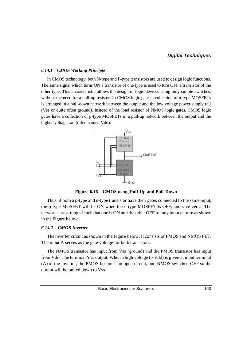
Digital Techniques
Basic Electronics for Seafarers 163
6.14.1 CMOS Working Principle
In CMOS technology, both N-type and P-type transistors are used to design logic functions.
The same signal which turns ON a transistor of one type is used to turn OFF a transistor of the
other type. This characteristic allows the design of logic devices using only simple switches,
without the need for a pull-up resistor. In CMOS logic gates a collection of n-type MOSFETs
is arranged in a pull-down network between the output and the low voltage power supply rail
(Vss or quite often ground). Instead of the load resistor of NMOS logic gates, CMOS logic
gates have a collection of p-type MOSFETs in a pull-up network between the output and the
higher-voltage rail (often named Vdd).
Figure 6.16 – CMOS using Pull-Up and Pull-Down
Thus, if both a p-type and n-type transistor have their gates connected to the same input,
the p-type MOSFET will be ON when the n-type MOSFET is OFF, and vice-versa. The
networks are arranged such that one is ON and the other OFF for any input pattern as shown
in the Figure below.
6.14.2 CMOS Inverter
The inverter circuit as shown in the Figure below. It consists of PMOS and NMOS FET.
The input A serves as the gate voltage for both transistors.
The NMOS transistor has input from Vss (ground) and the PMOS transistor has input
from Vdd. The terminal Y is output. When a high voltage (~ Vdd) is given at input terminal
(A) of the inverter, the PMOS becomes an open circuit, and NMOS switched OFF so the
output will be pulled down to Vss.
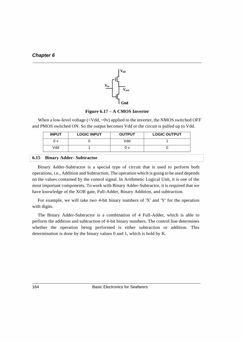
Chapter 6
Basic Electronics for Seafarers 164
Figure 6.17 – A CMOS Inverter
When a low-level voltage (<Vdd, ~0v) applied to the inverter, the NMOS switched OFF
and PMOS switched ON. So the output becomes Vdd or the circuit is pulled up to Vdd.
INPUT LOGIC INPUT OUTPUT LOGIC OUTPUT
0 v 0 Vdd 1
Vdd 1 0 v 0
6.15 Binary Adder- Subtractor
Binary Adder-Subtractor is a special type of circuit that is used to perform both
operations, i.e., Addition and Subtraction. The operation which is going to be used depends
on the values contained by the control signal. In Arithmetic Logical Unit, it is one of the
most important components. To work with Binary Adder-Subtractor, it is required that we
have knowledge of the XOR gate, Full-Adder, Binary Addition, and subtraction.
For example, we will take two 4-bit binary numbers of 'X' and 'Y' for the operation
with digits.
The Binary Adder-Subtractor is a combination of 4 Full-Adder, which is able to
perform the addition and subtraction of 4-bit binary numbers. The control line determines
whether the operation being performed is either subtraction or addition. This
determination is done by the binary values 0 and 1, which is hold by K.
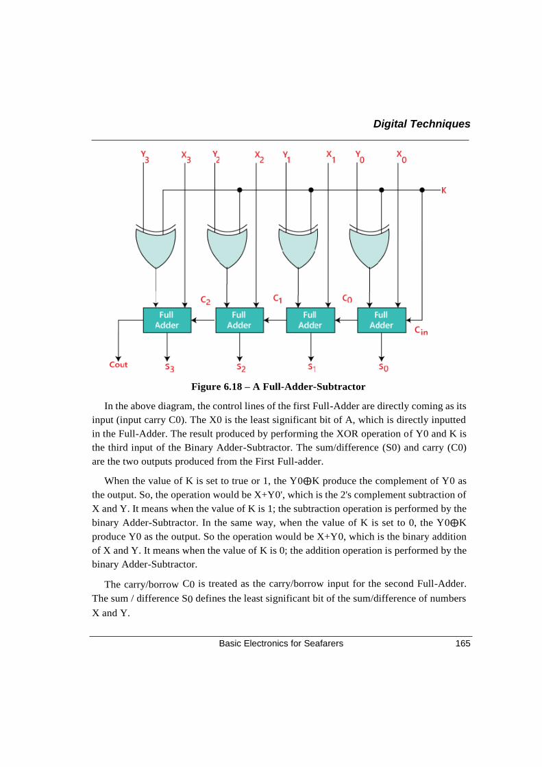
Digital Techniques
Basic Electronics for Seafarers 165
Figure 6.18 – A Full-Adder-Subtractor
In the above diagram, the control lines of the first Full-Adder are directly coming as its
input (input carry C0). The X0 is the least significant bit of A, which is directly inputted
in the Full-Adder. The result produced by performing the XOR operation of Y0 and K is
the third input of the Binary Adder-Subtractor. The sum/difference (S0) and carry (C0)
are the two outputs produced from the First Full-adder.
When the value of K is set to true or 1, the Y0⨁K produce the complement of Y0 as
the output. So, the operation would be X+Y0', which is the 2's complement subtraction of
X and Y. It means when the value of K is 1; the subtraction operation is performed by the
binary Adder-Subtractor. In the same way, when the value of K is set to 0, the Y0⨁K
produce Y0 as the output. So the operation would be X+Y0, which is the binary addition
of X and Y. It means when the value of K is 0; the addition operation is performed by the
binary Adder-Subtractor.
The carry/borrow C0 is treated as the carry/borrow input for the second Full-Adder.
The sum / difference S0 defines the least significant bit of the sum/difference of numbers
X and Y.
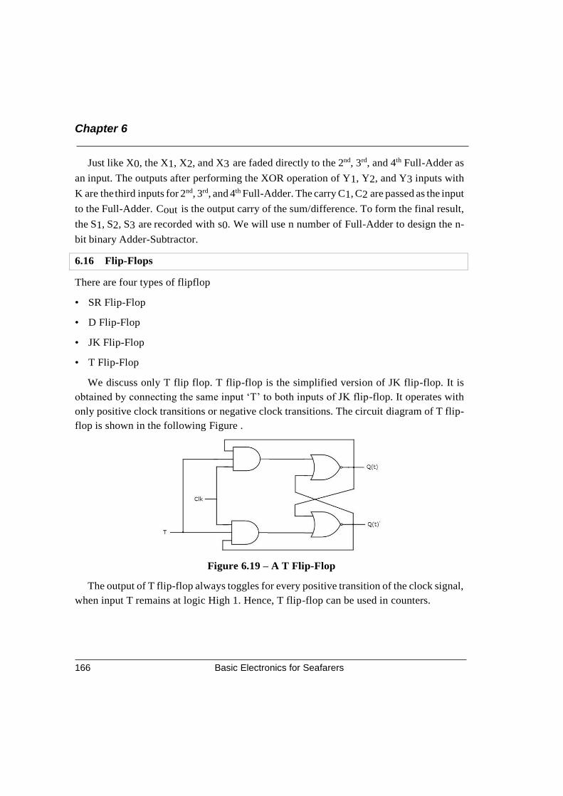
Chapter 6
Basic Electronics for Seafarers 166
Just like X0, the X1, X2, and X3 are faded directly to the 2nd, 3rd, and 4th Full-Adder as
an input. The outputs after performing the XOR operation of Y1, Y2, and Y3 inputs with
K are the third inputs for 2nd, 3rd, and 4th Full-Adder. The carry C1, C2 are passed as the input
to the Full-Adder. Cout is the output carry of the sum/difference. To form the final result,
the S1, S2, S3 are recorded with s0. We will use n number of Full-Adder to design the n-
bit binary Adder-Subtractor.
6.16 Flip-Flops
There are four types of flipflop
• SR Flip-Flop
• D Flip-Flop
• JK Flip-Flop
• T Flip-Flop
We discuss only T flip flop. T flip-flop is the simplified version of JK flip-flop. It is
obtained by connecting the same input ‘T’ to both inputs of JK flip-flop. It operates with
only positive clock transitions or negative clock transitions. The circuit diagram of T flip-
flop is shown in the following Figure .
Figure 6.19 – A T Flip-Flop
The output of T flip-flop always toggles for every positive transition of the clock signal,
when input T remains at logic High 1. Hence, T flip-flop can be used in counters.
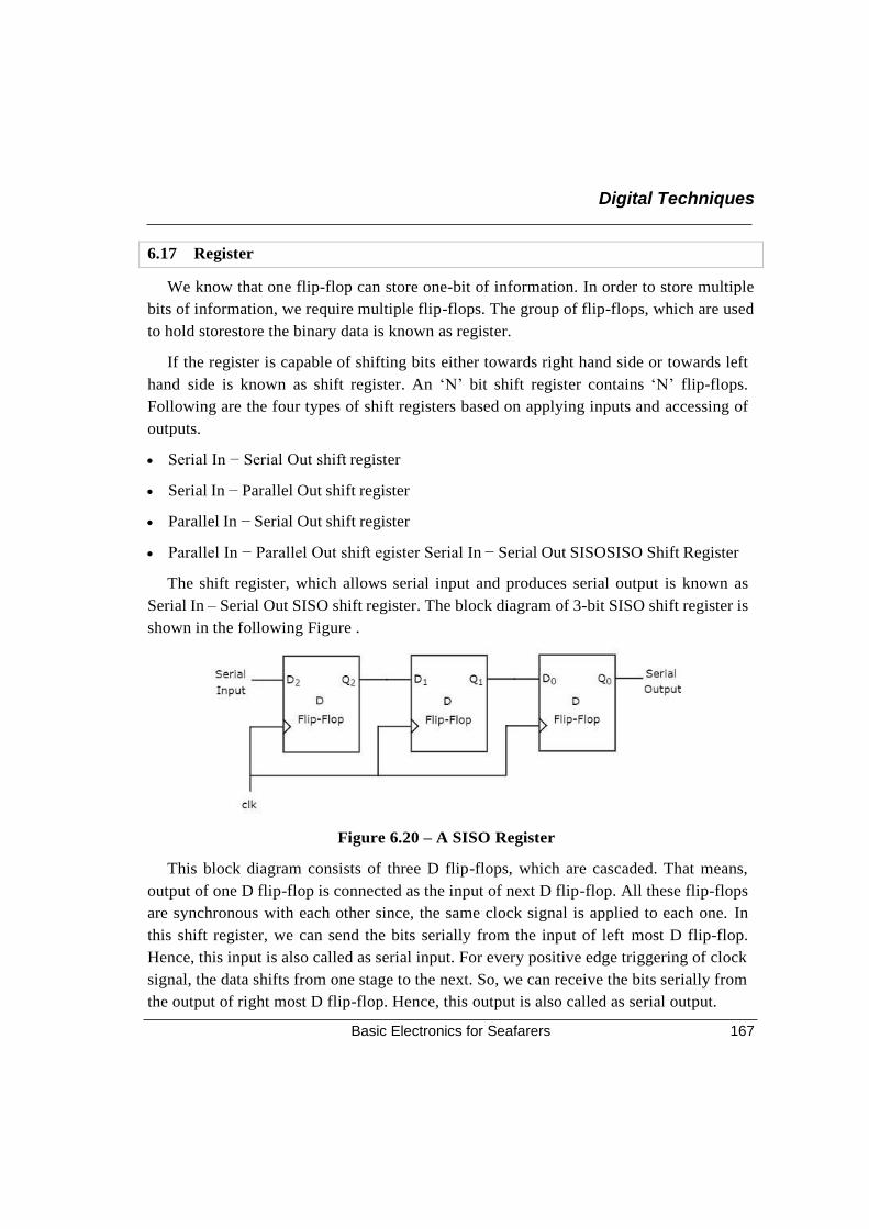
Digital Techniques
Basic Electronics for Seafarers 167
6.17 Register
We know that one flip-flop can store one-bit of information. In order to store multiple
bits of information, we require multiple flip-flops. The group of flip-flops, which are used
to hold storestore the binary data is known as register.
If the register is capable of shifting bits either towards right hand side or towards left
hand side is known as shift register. An ‘N’ bit shift register contains ‘N’ flip-flops.
Following are the four types of shift registers based on applying inputs and accessing of
outputs.
• Serial In − Serial Out shift register
• Serial In − Parallel Out shift register
• Parallel In − Serial Out shift register
• Parallel In − Parallel Out shift egister Serial In − Serial Out SISOSISO Shift Register
The shift register, which allows serial input and produces serial output is known as
Serial In – Serial Out SISO shift register. The block diagram of 3-bit SISO shift register is
shown in the following Figure .
Figure 6.20 – A SISO Register
This block diagram consists of three D flip-flops, which are cascaded. That means,
output of one D flip-flop is connected as the input of next D flip-flop. All these flip-flops
are synchronous with each other since, the same clock signal is applied to each one. In
this shift register, we can send the bits serially from the input of left most D flip-flop.
Hence, this input is also called as serial input. For every positive edge triggering of clock
signal, the data shifts from one stage to the next. So, we can receive the bits serially from
the output of right most D flip-flop. Hence, this output is also called as serial output.
Chapter 6
Basic Electronics for Seafarers 168
• A shift register is used as a Parallel to serial converter, which converts the parallel data
into serial data. It is utilized at the transmitter section after Analog to Digital Converter
ADC block.
• A Shift register is also used as a Serial to parallel converter, which converts the serial
data into parallel data. It is utilized at the receiver section before Digital to Analog
Converter DAC block.
6.18 Counter
An ‘N’ bit binary counter consists of ‘N’ T flip-flops. If the counter counts from 0 to 2𝑁 −
1, then it is called as binary up counter. Similarly, if the counter counts down from
2𝑁 − 1 to 0, then it is called as binary down counter.
There are two types of counters based on the flip-flops that are connected in
synchronous or not.
1. Asynchronous counters
2. Synchronous counters
6.18.1 Asynchronous Counters
If the flip-flops do not receive the same clock signal, then that counter is called as
Asynchronous counter. The output of system clock is applied as clock signal only to first
flip-flop. The remaining flip-flops receive the clock signal from output of its previous
stage flip-flop. Hence, the outputs of all flip-flops do not change affect at the same time.
There are two types:
1. Asynchronous Binary up counter
2. Asynchronous Binary down counter
6.18.2 Synchronous Counters
If all the flip-flops receive the same clock signal, then that counter is called as
Synchronous counter. Hence, the outputs of all flip-flops change affect at the same time.
There are two types:
1. Synchronous Binary up counter
2. Synchronous Binary down counter
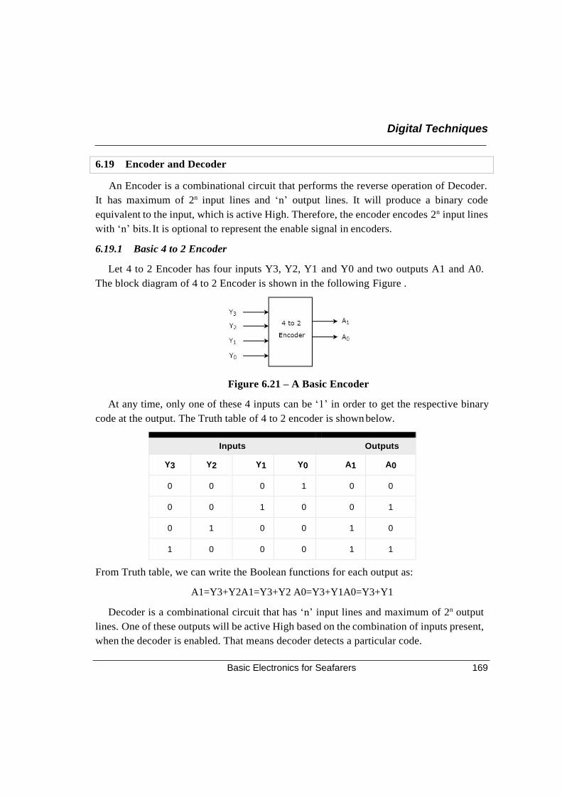
Digital Techniques
Basic Electronics for Seafarers 169
6.19 Encoder and Decoder
An Encoder is a combinational circuit that performs the reverse operation of Decoder.
It has maximum of 2n input lines and ‘n’ output lines. It will produce a binary code
equivalent to the input, which is active High. Therefore, the encoder encodes 2n input lines
with ‘n’ bits. It is optional to represent the enable signal in encoders.
6.19.1 Basic 4 to 2 Encoder
Let 4 to 2 Encoder has four inputs Y3, Y2, Y1 and Y0 and two outputs A1 and A0.
The block diagram of 4 to 2 Encoder is shown in the following Figure .
Figure 6.21 – A Basic Encoder
At any time, only one of these 4 inputs can be ‘1’ in order to get the respective binary
code at the output. The Truth table of 4 to 2 encoder is shown below.
Inputs Outputs
Y3 Y2 Y1 Y0 A1 A0
0 0 0 1 0 0
0 0 1 0 0 1
0 1 0 0 1 0
1 0 0 0 1 1
From Truth table, we can write the Boolean functions for each output as:
A1=Y3+Y2A1=Y3+Y2 A0=Y3+Y1A0=Y3+Y1
Decoder is a combinational circuit that has ‘n’ input lines and maximum of 2n output
lines. One of these outputs will be active High based on the combination of inputs present,
when the decoder is enabled. That means decoder detects a particular code.
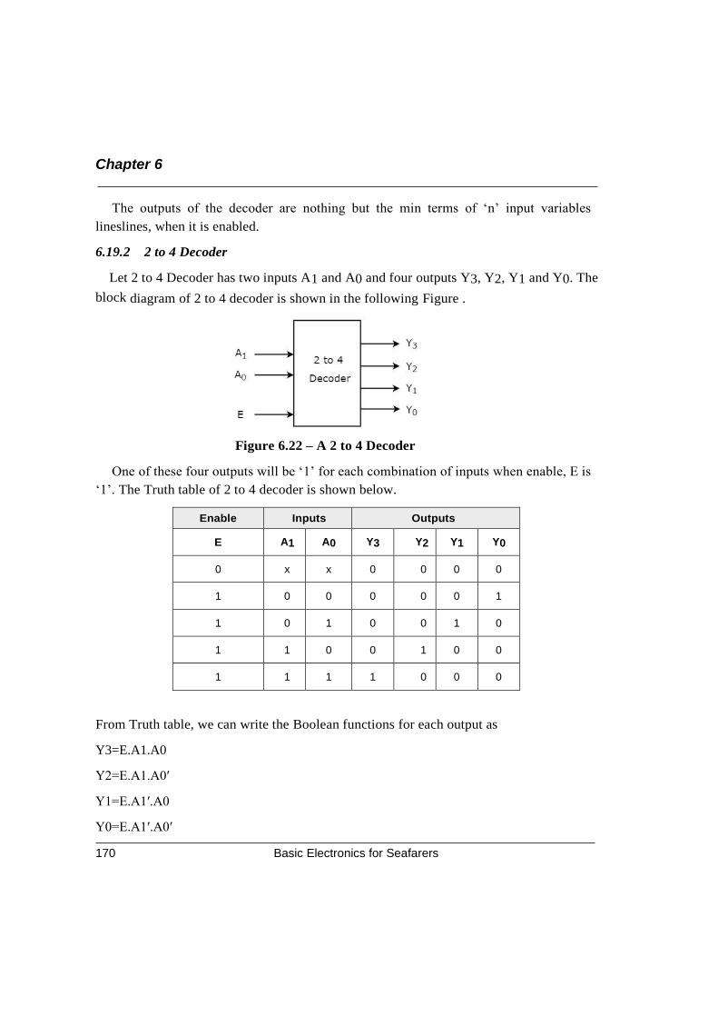
Chapter 6
Basic Electronics for Seafarers 170
The outputs of the decoder are nothing but the min terms of ‘n’ input variables
lineslines, when it is enabled.
6.19.2 2 to 4 Decoder
Let 2 to 4 Decoder has two inputs A1 and A0 and four outputs Y3, Y2, Y1 and Y0. The
block diagram of 2 to 4 decoder is shown in the following Figure .
Figure 6.22 – A 2 to 4 Decoder
One of these four outputs will be ‘1’ for each combination of inputs when enable, E is
‘1’. The Truth table of 2 to 4 decoder is shown below.
Enable Inputs Outputs
E A1 A0 Y3 Y2 Y1 Y0
0 x x 0 0 0 0
1 0 0 0 0 0 1
1 0 1 0 0 1 0
1 1 0 0 1 0 0
1 1 1 1 0 0 0
From Truth table, we can write the Boolean functions for each output as
Y3=E.A1.A0
Y2=E.A1.A0′
Y1=E.A1′.A0
Y0=E.A1′.A0′
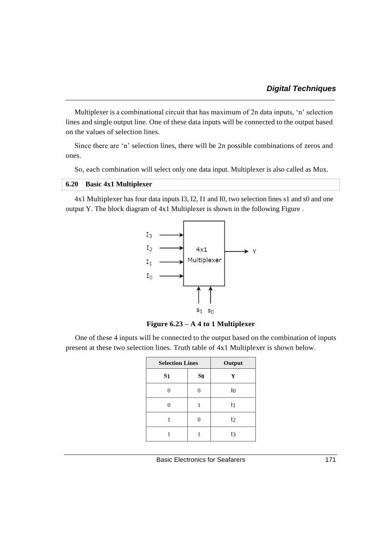
Digital Techniques
Basic Electronics for Seafarers 171
Multiplexer is a combinational circuit that has maximum of 2n data inputs, ‘n’ selection
lines and single output line. One of these data inputs will be connected to the output based
on the values of selection lines.
Since there are ‘n’ selection lines, there will be 2n possible combinations of zeros and
ones.
So, each combination will select only one data input. Multiplexer is also called as Mux.
6.20 Basic 4x1 Multiplexer
4x1 Multiplexer has four data inputs I3, I2, I1 and I0, two selection lines s1 and s0 and one
output Y. The block diagram of 4x1 Multiplexer is shown in the following Figure .
Figure 6.23 – A 4 to 1 Multiplexer
One of these 4 inputs will be connected to the output based on the combination of inputs
present at these two selection lines. Truth table of 4x1 Multiplexer is shown below.
Selection Lines Output
S1 S0 Y
0 0 I0
0 1 I1
1 0 I2
1 1 I3
Chapter 6
Basic Electronics for Seafarers 172
From the previous truth table, we can directly write the Boolean function for output, Y
as Y= S1′S0′I0+S1′S0I1+S1S0′I2+S1S0I3
6.21 Semiconductor Memory Technologies
A semiconductor memory is used in any electronics assembly that uses computer
processing technology. Semiconductor memory is the essential electronics component
needed for any computer-based PCB assembly.
In addition to this, memory cards have become commonplace items for temporarily
storing data - everything from the portable flash memory cards used for transferring files,
to semiconductor memory cards used in cameras, mobile phones and the like.
The use of semiconductor memory has grown, and the size of these memory cards has
increased as the need for larger and larger amounts of storage is needed.
To meet the growing needs for semiconductor memory, there are many types and
technologies that are used. As the demand grows new memory technologies are being
introduced and the existing types and technologies are being further developed.
A variety of different memory technologies are available - each one suited to different
applications. Names such as ROM, RAM, EPROM, EEPROM, Flash memory, DRAM,
SRAM, SDRAM, as well as F-RAM and MRAM are available, and new types are being
developed to enable improved performance.
Terms like DDR3, DDR4, DDR5 and many more are seen and these refer to different
types of SDRAM semiconductor memory.
In addition to this the semiconductor devices are available in many forms - ICs for
printed board assembly, USB memory cards, Compact Flash cards, SD memory cards and
even solid-state hard drives. Semiconductor memory is even incorporated into many
microprocessor chips as on-board memory.

Digital Techniques
Basic Electronics for Seafarers 173
Figure 6.24 – Printed circuit board containing computer memory
Semiconductor Memory Main Types
There are two main types or categories that can be used for semiconductor technology.
These memory types or categories differentiate the memory to the way in which it operates:
6.21.1 RAM - Random Access Memory
As the names suggest, the RAM or random-access memory is a form of semiconductor
memory technology that is used for reading and writing data in any order - in other words
as it is required by the processor. It is used for such applications as the computer or
processor memory where variables and other stored and are required on a random basis.
Data is stored and read many times to and from this type of memory. Random access
memory is used in huge quantities in computer applications as current day computing and
processing technology requires large amounts of memory to enable them to handle the
memory hungry applications used today. Many types of RAMs including the SDRAM with
its DDR3, DDR4, and soon DDR5 variants are used in huge quantities.
6.21.2 ROM - Read Only Memory
A ROM is a form of semiconductor memory technology used where the data is written
once and then not changed. I
n view of this it is used where data needs to be stored permanently, even when the power
is removed - many memory technologies lose the data once the power is removed.
As a result, this type of semiconductor memory technology is widely used for storing
programs and data that must survive when a computer or processor is powered down. For
example, the BIOS of a computer will be stored in ROM. As the name implies, data cannot
be easily written to ROM.
Chapter 6
Basic Electronics for Seafarers 174
Depending on the technology used in the ROM, writing the data into the ROM initially
may require special hardware. Although it is often possible to change the data, this gain
requires special hardware to erase the data ready for new data to be written in.
As can be seen, these two types of memory are very different, and as a result they are
used in very different ways.
Each of the semiconductor memory technologies outlined below falls into one of these
two types. Each technology offers its own advantages and is used in a particular way, or
for a particular application.
6.21.3 RAM - Random Access Memory
As the names suggest, the RAM or random-access memory is a form of semiconductor
memory technology that is used for reading and writing data in any order - in other words
as it is required by the processor.
It is used for such applications as the computer or processor memory where variables
and other stored and are required on a random basis.
Data is stored and read many times to and from this type of memory. Random access
memory is used in huge quantities in computer applications as current day computing and
processing technology requires large amounts of memory to enable them to handle the
memory hungry applications used today. Many types of RAM including SDRAM with its
DDR3, DDR4, and soon DDR5 variants are used in huge quantities.
6.21.4 ROM - Read Only Memory
A ROM is a form of semiconductor memory technology used where the data is written
once and then not changed. In view of this it is used where data needs to be stored
permanently, even when the power is removed - many memory technologies lose the data
once the power is removed.
As a result, this type of semiconductor memory technology is widely used for storing
programs and data that must survive when a computer or processor is powered down. For
example, the BIOS of a computer will be stored in ROM. As the name implies, data cannot
be easily written to ROM. Depending on the technology used in the ROM, writing the data
into the ROM initially may require special hardware. Although it is often possible to change
the data, this gain requires special hardware to erase the data ready for new data to be
written in.
Digital Techniques
Basic Electronics for Seafarers 175
As can be seen, these two types of memory are very different, and as a result they are
used in very different ways.
Each of the semiconductor memory technologies outlined below falls into one of these
two categories. each technology offers its own advantages and is used in a particular way,
or for a particular application.
There is a large variety of types of ROM and RAM that are available. Often the overall
name for the memory technology includes the initials RAM or ROM and this gives a guide
as to the overall type of format for the memory.
With technology moving forwards apace, not only are the established technologies
moving forwards with SDRAM technology moving from DDR3 to DDR4 and then to
DDR5, but Flash memory used in memory cards is also developing as are the other
technologies.
In addition to this, new memory technologies are arriving on the scene and they are
starting to make an impact in the market, enabling processor circuits to perform more
effectively.
The different memory types or memory technologies are detailed below:
6.21.5 DRAM
Dynamic RAM is a form of random-access memory. DRAM uses a capacitor to store
each bit of data, and the level of charge on each capacitor determines whether that bit is a
logical 1 or 0. However these capacitors do not hold their charge indefinitely, and therefore
the data needs to be refreshed periodically. As a result of this dynamic refreshing, it gains
its name of being a dynamic RAM. DRAM is the form of semiconductor memory that is
often used in equipment including personal computers and workstations where it forms the
main RAM for the computer. The semiconductor devices are normally available as
integrated circuits for use in PCB assembly in the form of surface mount devices or less
frequently now as leaded components.
6.21.6 EEPROM
This is an Electrically Erasable Programmable Read Only Memory. Data can be written
to these semiconductor devices and it can be erased using an electrical voltage.
Chapter 6
Basic Electronics for Seafarers 176
This is typically applied to an erase pin on the chip. Like other types of PROMS,
EEPROM retains the contents of the memory even when the power is turned off. Also, like
other types of ROM, EEPROM is not as fast as RAM.
6.21.7 EPROM
This is an Erasable Programmable Read Only Memory. These semiconductor devices
can be programmed and then erased at a later time. This is normally achieved by exposing
the semiconductor device itself to ultraviolet light. To enable this to happen there is a
circular window in the package of the EPROM to enable the light to reach the silicon of the
device. When the PROM is in use, this window is normally covered by a label, especially
when the data may need to be preserved for an extended period. The PROM stores its data
as a charge on a capacitor.
There is a charge storage capacitor for each cell and this can be read repeatedly as
required. However, it is found that after many years the charge may leak away and the data
may be lost. Nevertheless, this type of semiconductor memory used to be widely used in
applications where a form of ROM was required, but where the data needed to be changed
periodically, as in a development environment, or where quantities were low.
6.21.8 Flash Memory
Flash memory may be considered as a development of EEPROM technology. Data can
be written to it and it can be erased, although only in blocks, but data can be read on an
individual cell basis. To erase and re-programme areas of the chip, programming voltages
at levels that are available within electronic equipment are used. It is also non-volatile, and
this makes it particularly useful. As a result, Flash memory is widely used in many
applications including USB memory sticks, compact Flash memory cards, SD memory cards
and also now solid-state hard drives for computers and many other applications.
6.21.9 F-RAM
Ferroelectric RAM is a random-access memory technology that has many similarities
to the standard DRAM technology. The major difference is that it incorporates a
ferroelectric layer instead of the more usual dielectric layer and this provides its non-
volatile capability. As it offers a non-volatile capability, F-RAM is a direct competitor to
Flash.
Digital Techniques
Basic Electronics for Seafarers 177
6.21.10 M-RAM
This is Magneto-resistive RAM, or Magnetic RAM. It is a non-volatile RAM memory
technology that uses magnetic charges to store data instead of electric charges. Unlike
technologies including DRAM, which require a constant flow of electricity to maintain the
integrity of the data, MRAM retains data even when the power is removed. An additional
advantage is that it only requires low power for active operation. As a result, this
technology could become a major player in the electronics industry now that production
processes have been developed to enable it to be produced.
6.21.11 P-RAM / PCM
This type of semiconductor memory is known as Phase change Random Access
Memory, P-RAM or just Phase Change memory, PCM. It is based around a phenomenon
where a form of chalcogenide glass changes is state or phase between an amorphous state
(high resistance) and a polycrystalline state (low resistance).
It is possible to detect the state of an individual cell and hence use this for data storage.
Currently this type of memory has not been widely commercialised, but it is expected to
be a competitor for flash memory.
6.21.12 PROM
This stands for Programmable Read Only Memory. It is a semiconductor memory which
can only have data written to it once - the data written to it is permanent.
These memories are bought in a blank format and they are programmed using a special
PROM programmer. Typically, a PROM will consist of an array of fuseable links some of
which are "blown" during the programming process to provide the required data pattern.
6.21.13 SDRAM
Synchronous DRAM. This form of semiconductor memory can run at faster speeds than
conventional DRAM. It is synchronised to the clock of the processor and is capable of
keeping two sets of memory addresses open simultaneously. By transferring data alternately
from one set of addresses, and then the other, SDRAM cuts down on the delays associated
with non-synchronous RAM, which must close one address bank before opening the next.
Within the SDRAM family there are several types of memory technologies that are seen.
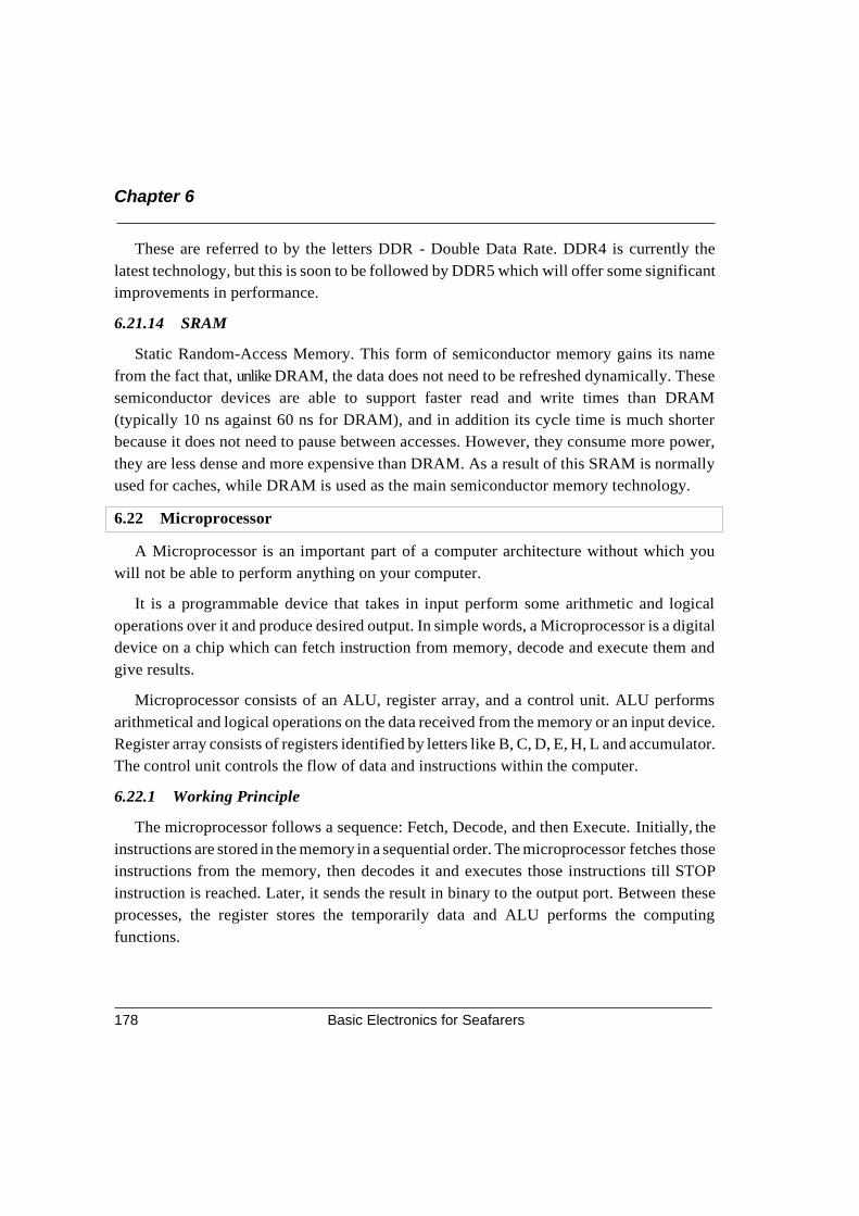
Chapter 6
Basic Electronics for Seafarers 178
These are referred to by the letters DDR - Double Data Rate. DDR4 is currently the
latest technology, but this is soon to be followed by DDR5 which will offer some significant
improvements in performance.
6.21.14 SRAM
Static Random-Access Memory. This form of semiconductor memory gains its name
from the fact that, unlike DRAM, the data does not need to be refreshed dynamically. These
semiconductor devices are able to support faster read and write times than DRAM
(typically 10 ns against 60 ns for DRAM), and in addition its cycle time is much shorter
because it does not need to pause between accesses. However, they consume more power,
they are less dense and more expensive than DRAM. As a result of this SRAM is normally
used for caches, while DRAM is used as the main semiconductor memory technology.
6.22 Microprocessor
A Microprocessor is an important part of a computer architecture without which you
will not be able to perform anything on your computer.
It is a programmable device that takes in input perform some arithmetic and logical
operations over it and produce desired output. In simple words, a Microprocessor is a digital
device on a chip which can fetch instruction from memory, decode and execute them and
give results.
Microprocessor consists of an ALU, register array, and a control unit. ALU performs
arithmetical and logical operations on the data received from the memory or an input device.
Register array consists of registers identified by letters like B, C, D, E, H, L and accumulator.
The control unit controls the flow of data and instructions within the computer.
6.22.1 Working Principle
The microprocessor follows a sequence: Fetch, Decode, and then Execute. Initially, the
instructions are stored in the memory in a sequential order. The microprocessor fetches those
instructions from the memory, then decodes it and executes those instructions till STOP
instruction is reached. Later, it sends the result in binary to the output port. Between these
processes, the register stores the temporarily data and ALU performs the computing
functions.
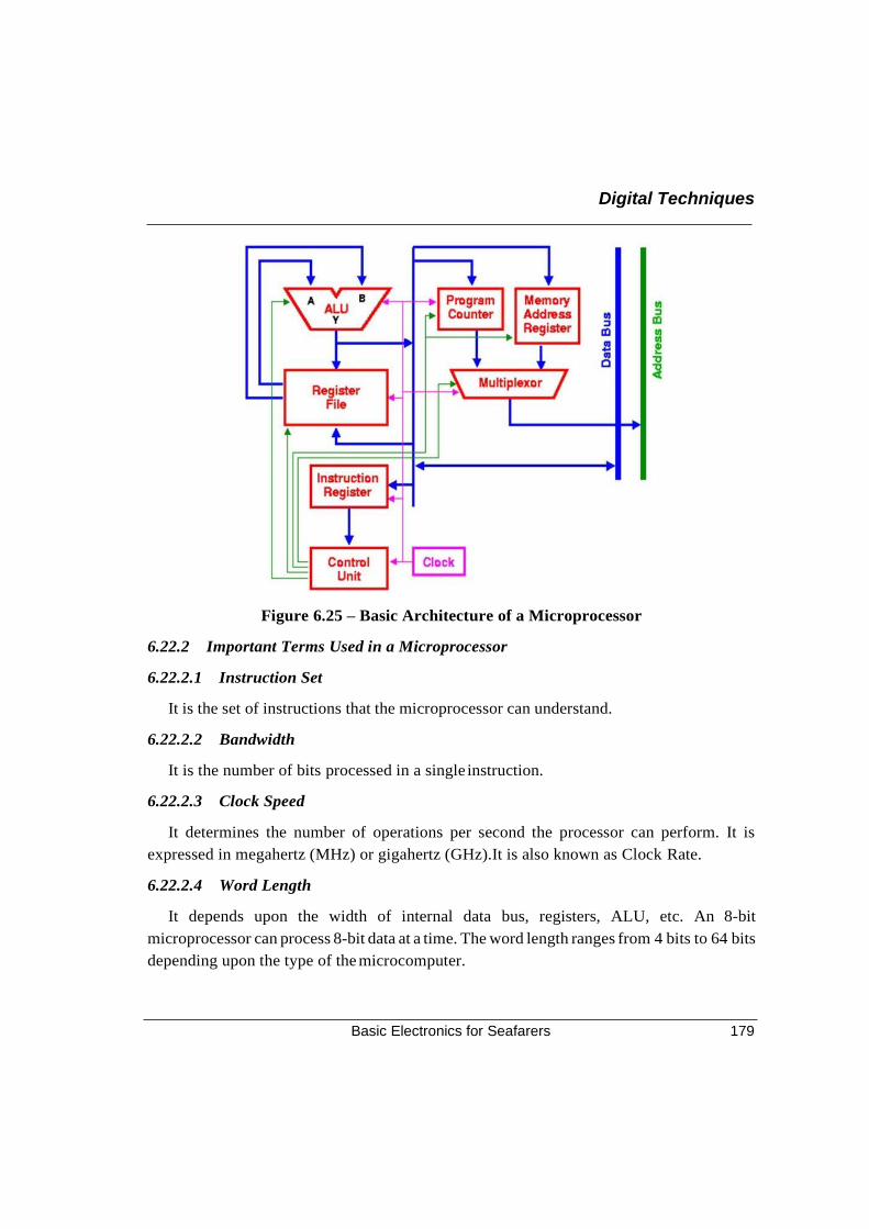
Digital Techniques
Basic Electronics for Seafarers 179
Figure 6.25 – Basic Architecture of a Microprocessor
6.22.2 Important Terms Used in a Microprocessor
6.22.2.1 Instruction Set
It is the set of instructions that the microprocessor can understand.
6.22.2.2 Bandwidth
It is the number of bits processed in a single instruction.
6.22.2.3 Clock Speed
It determines the number of operations per second the processor can perform. It is
expressed in megahertz (MHz) or gigahertz (GHz).It is also known as Clock Rate.
6.22.2.4 Word Length
It depends upon the width of internal data bus, registers, ALU, etc. An 8-bit
microprocessor can process 8-bit data at a time. The word length ranges from 4 bits to 64 bits
depending upon the type of the microcomputer.
Chapter 6
Basic Electronics for Seafarers 180
6.22.2.5 Data Types
The microprocessor has multiple data type formats like binary, BCD, ASCII, signed and
unsigned numbers.
6.22.3 Functional Parts
6.22.3.1 ALU
Arithmetic and logic unit, As the name suggests, it performs arithmetic and logical
operations like Addition, Subtraction, AND, OR, etc.
6.22.3.2 Instruction Sets and Registers
The group of instructions a processor can execute are called its "instruction set." The
instruction set determines things such as the type of programs a CPU can work with.
Registers are small memory locations that also contain instructions. Unlike regular memory
locations, registers are referred to by a name instead of a number. For example, the IP
(instruction pointer) contains the location of the next instruction, and the "accumulator"
is where the processor stores the next value it plans to work on.
6.22.3.3 Cache Memory
Cache memory is an area on the CPU where copies of common instructions required to
perform functions and run programs are stored temporarily. Since the processor has its own
smaller, faster cache memory, it can process data more quickly than reading and writing to
the main system memory. Types of microprocessor memory include ROM (read-only) and
RAM (random-access).
6.22.3.4 Bus
Connection lines used to connect the internal parts of the microprocessor chip is called
bus. There are three types of buses in a microprocessor. Data bus, address bus, control bus.
6.22.3.5 Input Output Interface
Input-Output Interface is used as a method which helps in transferring of information
between the internal storage devices i.e., memory and the external peripheral device. A
peripheral device is that which provide input and output for the computer, it is also called
an I/O device e.g., a keyboard and mouse provide Input to the computer are called input
devices while a monitor and printer that provide output to the computer are called output
devices. Just like the external hard-drives, there is also availability of some peripheral
devices which are able to provide both input and output.
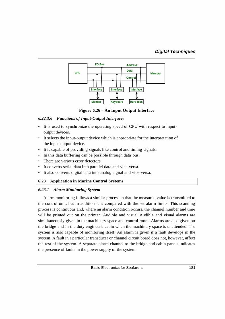
Digital Techniques
Basic Electronics for Seafarers 181
Figure 6.26 – An Input Output Interface
6.22.3.6 Functions of Input-Output Interface:
• It is used to synchronize the operating speed of CPU with respect to input-
output devices.
• It selects the input-output device which is appropriate for the interpretation of
the input-output device.
• It is capable of providing signals like control and timing signals.
• In this data buffering can be possible through data bus.
• There are various error detectors.
• It converts serial data into parallel data and vice-versa.
• It also converts digital data into analog signal and vice-versa.
6.23 Application in Marine Control Systems
6.23.1 Alarm Monitoring System
Alarm monitoring follows a similar process in that the measured value is transmitted to
the control unit, but in addition it is compared with the set alarm limits. This scanning
process is continuous and, where an alarm condition occurs, the channel number and time
will be printed out on the printer. Audible and visual Audible and visual alarms are
simultaneously given in the machinery space and control room. Alarms are also given on
the bridge and in the duty engineer's cabin when the machinery space is unattended. The
system is also capable of monitoring itself. An alarm is given if a fault develops in the
system. A fault in a particular transducer or channel circuit board does not, however, affect
the rest of the system. A separate alarm channel to the bridge and cabin panels indicates
the presence of faults in the power supply of the system
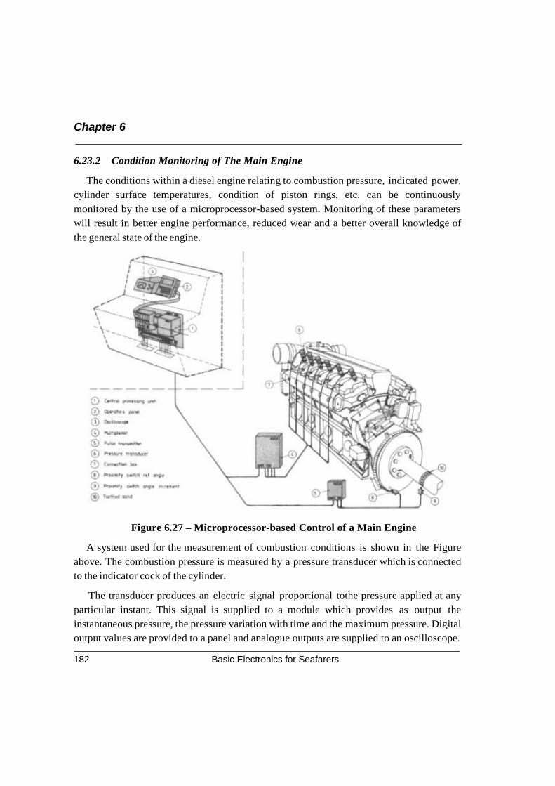
Chapter 6
Basic Electronics for Seafarers 182
6.23.2 Condition Monitoring of The Main Engine
The conditions within a diesel engine relating to combustion pressure, indicated power,
cylinder surface temperatures, condition of piston rings, etc. can be continuously
monitored by the use of a microprocessor-based system. Monitoring of these parameters
will result in better engine performance, reduced wear and a better overall knowledge of
the general state of the engine.
Figure 6.27 – Microprocessor-based Control of a Main Engine
A system used for the measurement of combustion conditions is shown in the Figure
above. The combustion pressure is measured by a pressure transducer which is connected
to the indicator cock of the cylinder.
The transducer produces an electric signal proportional tothe pressure applied at any
particular instant. This signal is supplied to a module which provides as output the
instantaneous pressure, the pressure variation with time and the maximum pressure. Digital
output values are provided to a panel and analogue outputs are supplied to an oscilloscope.
Digital Techniques
Basic Electronics for Seafarers 183
The crankshaft rotation angle is measured by two proximity switches. One reads the
incremental angle from the flywheel teeth or a toothed band on the shaft. The other is a
reference point which is the top dead centre position for the cylinder nearest to the
flywheel. The pulses from the proximity switches are passed to a transmitter where they are
modified and then pass to the central processing unit.
The multiplexer transmits the pressure signals, cylinder by cylinder, to the central
processing unit.
The operator's panel communicates with the central processing unit to enable display, as
digital values, of mean indicated combustion pressure, indicated power, engine speed,
maximum combustion pressure, compression pressure and ignition angle.
Diagrams can be displayed on the oscilloscope of pressure against crank angle and peak
pressure against time. The system incorporates several test and calibration functions which
enable simple operation and fault tracing.
For each particular installation, parameters such as firing order, swept volume,
connecting rod length and stroke length are pre-programmed into the microcomputer
memory.
The program will also contain the appropriate mathematics to generate the output
functions from the input data. T he fitting of appropriate sensors and suitable programming
of the microcomputer will enable many other engine conditions to be monitored. One
example is the use of thermoelement surface temperature sensors inserted into cylinder
liners. The liner surface temperature can then be continuously monitored.
6.23.3 Generator Plant Control
• Integrated control
• Integrated bridge control
• Integrated ship instrumentation system
• Cargo control system
6.24 The 8085 Microprocessor
The 8085 microprocessor is pronounced as the "eighty-eighty-five" microprocessor. It
is an 8-bit microprocessor designed by Intel in 1977 using NMOS technology. It is a very
basic type of microprocessor that is used in washing machines, microwave ovens, mobile
phones, etc.
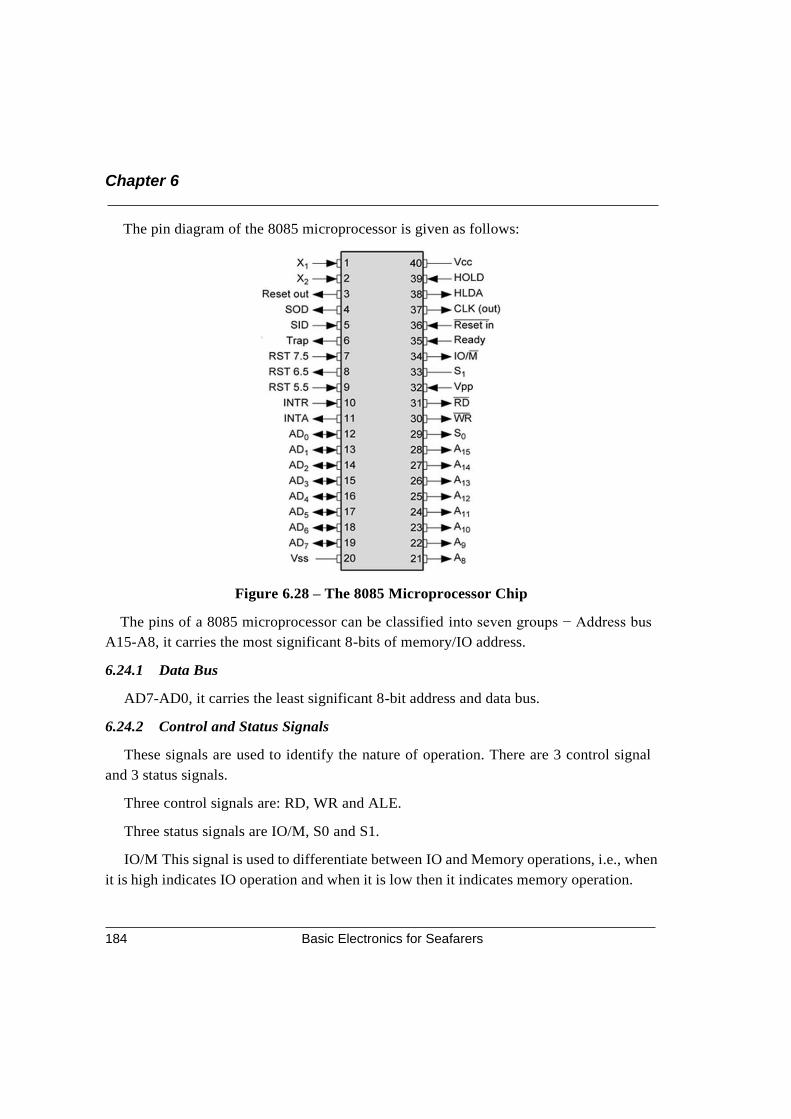
Chapter 6
Basic Electronics for Seafarers 184
The pin diagram of the 8085 microprocessor is given as follows:
Figure 6.28 – The 8085 Microprocessor Chip
The pins of a 8085 microprocessor can be classified into seven groups − Address bus
A15-A8, it carries the most significant 8-bits of memory/IO address.
6.24.1 Data Bus
AD7-AD0, it carries the least significant 8-bit address and data bus.
6.24.2 Control and Status Signals
These signals are used to identify the nature of operation. There are 3 control signal
and 3 status signals.
Three control signals are: RD, WR and ALE.
Three status signals are IO/M, S0 and S1.
IO/M This signal is used to differentiate between IO and Memory operations, i.e., when
it is high indicates IO operation and when it is low then it indicates memory operation.
Digital Techniques
Basic Electronics for Seafarers 185
6.24.3 S1 and S0
These signals are used to identify the type of current operation.
6.24.4 Power Supply
There are 2 power supply signals − VCC and VSS. VCC indicates +5v power supply
and VSS indicates ground signal.
6.24.5 Clock Signals
There are 3 clock signals, i.e. X1, X2, CLK OUT.
6.24.6 X1, X2 − A crystal (RC, LC N/W) is connected at these two pins and is used to
set frequency of the internal clock generator. This frequency is internally divided by 2.
6.24.7 CLK OUT − This signal is used as the system clock for devices connected with
the microprocessor.
6.24.8 Interrupts and Externally Initiated Signals
Interrupts are the signals generated by external devices to request the microprocessor to
perform a task. There are 5 interrupt signals, i.e. TRAP, RST 7.5, RST 6.5, RST 5.5, and
INTR. We will discuss interrupts in detail in interrupts section.
6.24.9 INTA − It is an interrupt acknowledgment signal.
6.24.10 RESET IN − This signal is used to reset the microprocessor by setting the
program counter to zero.
6.24.11 RESET OUT − This signal is used to reset all the connected devices when the
microprocessor is reset.
6.24.12 READY − This signal indicates that the device is ready to send or receive data.
If READY is low, then the CPU has to wait for READY to go high.
6.24.13 HOLD − This signal indicates that another master is requesting the use of the
address and data buses.
6.24.14 HLDA (HOLD Acknowledge) − It indicates that the CPU has received the HOLD
request and it will relinquish the bus in the next clock cycle. HLDA is set to low after the
HOLD signal is removed.
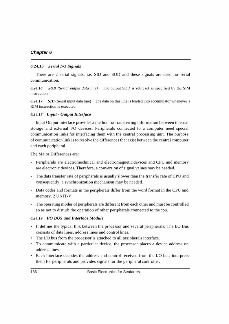
Chapter 6
Basic Electronics for Seafarers 186
6.24.15 Serial I/O Signals
There are 2 serial signals, i.e. SID and SOD and these signals are used for serial
communication.
6.24.16 SOD (Serial output data line) − The output SOD is set/reset as specified by the SIM
instruction.
6.24.17 SID (Serial input data line) − The data on this line is loaded into accumulator whenever a
RIM instruction is executed.
6.24.18 Input - Output Interface
Input Output Interface provides a method for transferring information between internal
storage and external I/O devices. Peripherals connected to a computer need special
communication links for interfacing them with the central processing unit. The purpose
of communication link is to resolve the differences that exist between the central computer
and each peripheral.
The Major Differences are:
• Peripherals are electromechnical and electromagnetic devices and CPU and memory
are electronic devices. Therefore, a conversion of signal values may be needed.
• The data transfer rate of peripherals is usually slower than the transfer rate of CPU and
consequently, a synchronization mechanism may be needed.
• Data codes and formats in the peripherals differ from the word format in the CPU and
memory. 2 UNIT-V
• The operating modes of peripherals are different from each other and must be controlled
so as not to disturb the operation of other peripherals connected to the cpu.
6.24.19 I/O BUS and Interface Module
• It defines the typical link between the processor and several peripherals. The I/O Bus
consists of data lines, address lines and control lines.
• The I/O bus from the processor is attached to all peripherals interface.
• To communicate with a particular device, the processor places a device address on
address lines.
• Each Interface decodes the address and control received from the I/O bus, interprets
them for peripherals and provides signals for the peripheral controller.
Digital Techniques
Basic Electronics for Seafarers 187
• It also synchronizes the data flow and supervises the transfer between peripheral and
processor.
Figure 6.29 – I/O BUS and Interface Module
6.25 One-Time-Programmable Memory (OTP)
While the memory contents for a ROM are set at design/manufacturing time,
Programmable Read Only memories (PROM) and more recently One-Time Programmable
(OTP) devices can be programmed after manufacturing making them a lot more flexible.
Once programmed, or blown, the contents cannot be changed and the contents are retained
after power is removed.
The term “blown” is a historical term related to the programming mechanism of
PROMs.
Contents were written by using a high voltage to burn out interconnection fuses. These
PROMs were blown on special devices called PROM Programmers.
The PROM was originally developed as part of a military program related to ICBMs
in 1956. The invention is attributed to Wen Tsing Chow who was working for American
Bosch Arma Corporation. Commercial devices became available in the late 1960s.
The integration of PROM technology into a standard CMOS process is attributed to
Kilopass Technology Inc. Kilopass has 1T, 2T and 3.5T antifuse bit cells and have been
available since 2001. In 2005, Sidense developed a split channel antifuse 1T device.
Synopsys has since acquired both Sidense and Kilopass.
6.26 NOR Flash Memory
Flash memory is NON volatile memory and currently very popular. Two the most
popular types are: NOR and NAND flash memory.
Chapter 6
Basic Electronics for Seafarers 188
NOR memory is used for storing code and execution. Allows quick random access to any
location in memory array.
NAND memory is used for data storage. Requires relatively long random access.
Programming and erasing is easier than in NAND memory. Cost of bit of NAND
memory is cheaper that NOR memory.
Flash memory architecture based on floating gate technology. In NOR flash memory
every memory cell is connected to the floating gate. In NAND flash memory, several
memory cells are connected in parallel.
NOR flash memory works on bit level. Due to the accessibility of every single bits in
NOR flash memory, it is slow comparatively. It is normally used for ROM memory. It is
comparatively expensive than NAND memory.
6.27 GPIO
A GPIO is a signal pin on an integrated circuit or board that can be used to perform
digital input or output functions. By design it has no predefined purpose and can be used by
the hardware or software developer to perform the functions they choose.
Typical applications include controlling LEDs, reading switches and controlling various
types of sensors.
The most common functions of GPIO pins include:
• Being configurable in software to be input or output
• Being enabled or disabled
• Setting the value of a digital output
• Reading the value of a digital output
• Generating an interrupt when the input changes value
GPIO pins are digital, meaning they only support high/low or on/off levels. They
generally don't support analog input or output with many discrete voltage levels.
Digital Techniques
Basic Electronics for Seafarers 189
6.27.1 Objectives
General Purpose I/O (GPIO) pins are single need to be provided to be versatile to digital
and analog signals for ADC conversions. To provide efficiency the signals must be signals
individually controllable on a particular chip board. Each GPIO should be able to define
either an input mode or an output mode for individual pins on the chip.
Finally, the pins must be extendable for a wide array of applications and functional uses
that define its generality in use.
6.27.2 GPIO on the LM3S89
On the LM3S8962 the GPIO modules consist of seven separate blocks, each of these
blocks will corresponding to individual ports on the GPIO interface, the ports in order are:
(Port A, Port B, Port C, Port D, Port E, Port F, Port G). The GPIO module on this board
supports up to 42 programmable input or output pins depending on the specific
configuration being chosen.
Some of the features of the ports include: a standard logic tolerance of up to 5-V on
both input and output, specific programmable control for GPIO interrupts which include
interrupt generation masking, ADC sampling, programmable control for GPIO pad,
digital input enables and open drain enables.
On the 8962 the data control registers allow software to conFigure the separate
programmable modes on the GPIOs. This is done by configuring the data direction
registers on the pins as either input or output for the lines. The data registers themselves
will contain information to be driven out of the system or new data that’s entered the
system. An example of the seven physical blocks of the GPIO is illustrated below:
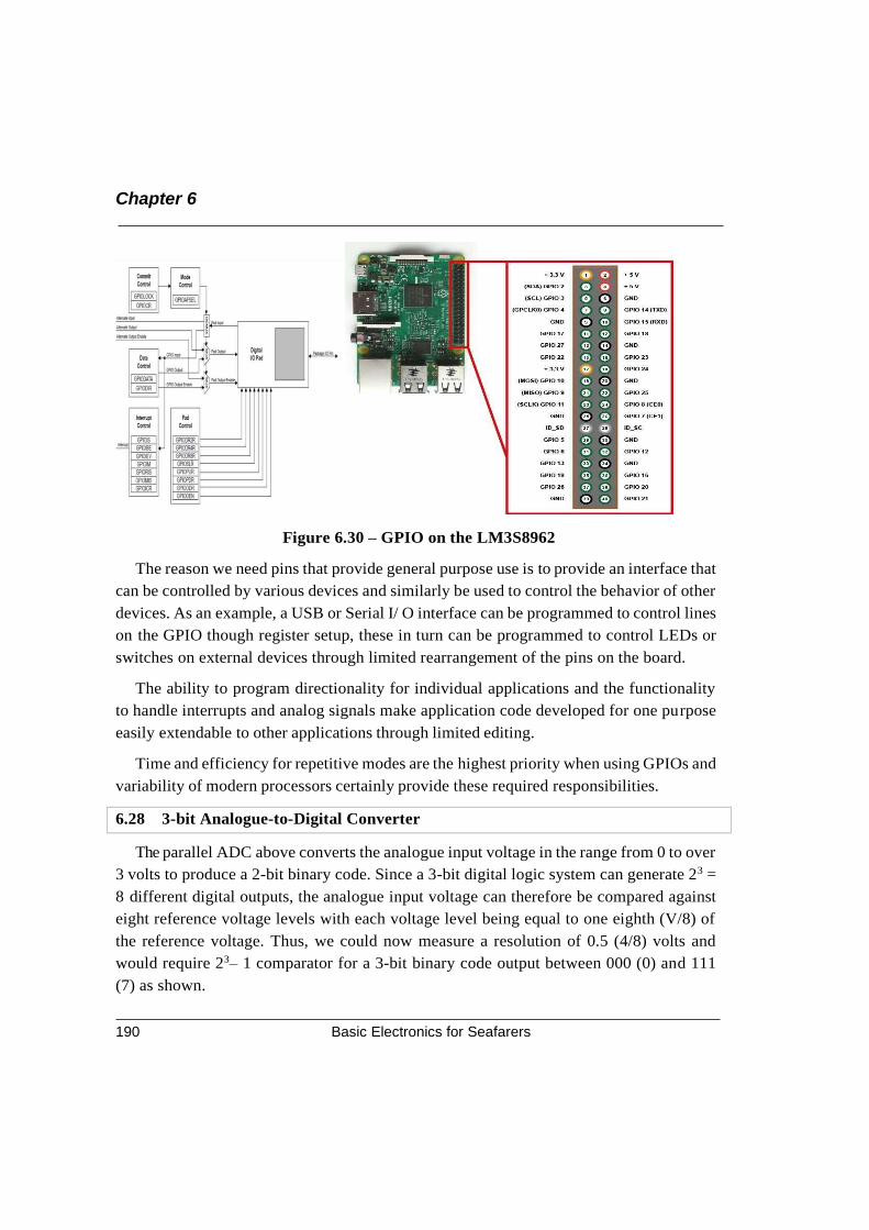
Chapter 6
Basic Electronics for Seafarers 190
Figure 6.30 – GPIO on the LM3S8962
The reason we need pins that provide general purpose use is to provide an interface that
can be controlled by various devices and similarly be used to control the behavior of other
devices. As an example, a USB or Serial I/ O interface can be programmed to control lines
on the GPIO though register setup, these in turn can be programmed to control LEDs or
switches on external devices through limited rearrangement of the pins on the board.
The ability to program directionality for individual applications and the functionality
to handle interrupts and analog signals make application code developed for one purpose
easily extendable to other applications through limited editing.
Time and efficiency for repetitive modes are the highest priority when using GPIOs and
variability of modern processors certainly provide these required responsibilities.
6.28 3-bit Analogue-to-Digital Converter
The parallel ADC above converts the analogue input voltage in the range from 0 to over
3 volts to produce a 2-bit binary code. Since a 3-bit digital logic system can generate 23 =
8 different digital outputs, the analogue input voltage can therefore be compared against
eight reference voltage levels with each voltage level being equal to one eighth (V/8) of
the reference voltage. Thus, we could now measure a resolution of 0.5 (4/8) volts and
would require 23– 1 comparator for a 3-bit binary code output between 000 (0) and 111
(7) as shown.
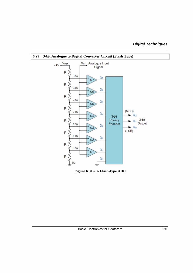
Digital Techniques
Basic Electronics for Seafarers 191
6.29 3-bit Analogue to Digital Converter Circuit (Flash Type)
Figure 6.31 – A Flash-type ADC
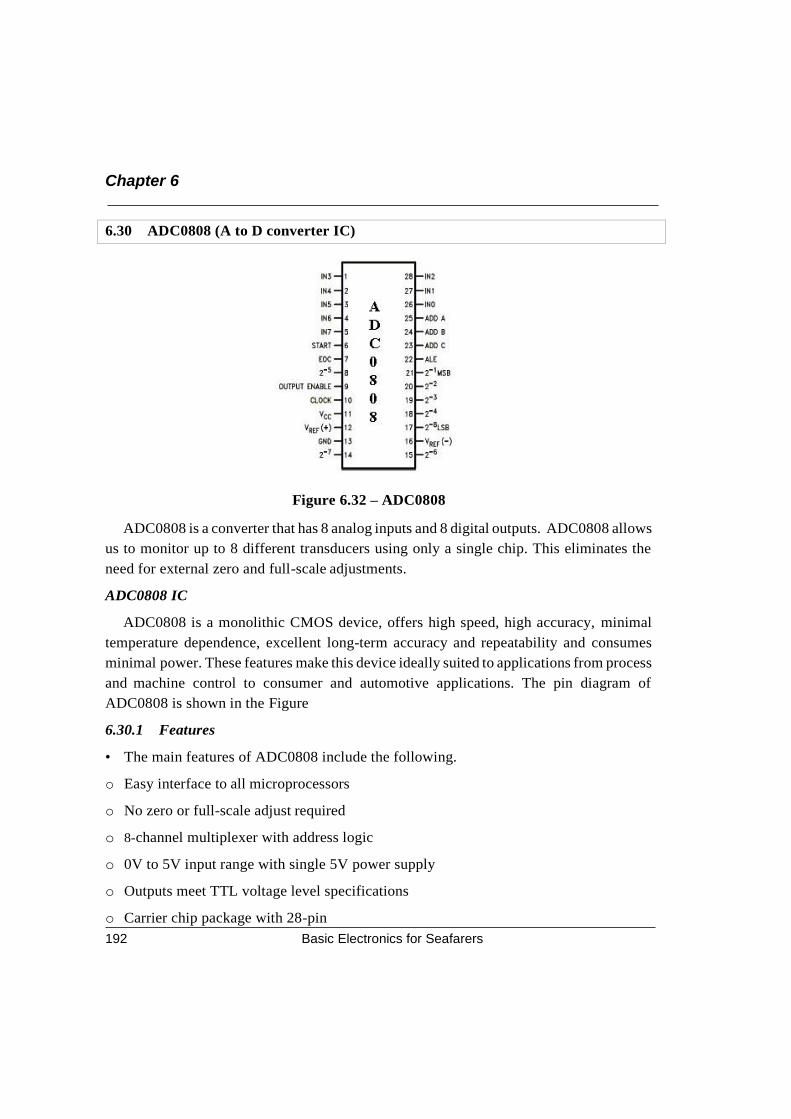
Chapter 6
Basic Electronics for Seafarers 192
6.30 ADC0808 (A to D converter IC)
Figure 6.32 – ADC0808
ADC0808 is a converter that has 8 analog inputs and 8 digital outputs. ADC0808 allows
us to monitor up to 8 different transducers using only a single chip. This eliminates the
need for external zero and full-scale adjustments.
ADC0808 IC
ADC0808 is a monolithic CMOS device, offers high speed, high accuracy, minimal
temperature dependence, excellent long-term accuracy and repeatability and consumes
minimal power. These features make this device ideally suited to applications from process
and machine control to consumer and automotive applications. The pin diagram of
ADC0808 is shown in the Figure
6.30.1 Features
• The main features of ADC0808 include the following.
o Easy interface to all microprocessors
o No zero or full-scale adjust required
o 8-channel multiplexer with address logic
o 0V to 5V input range with single 5V power supply
o Outputs meet TTL voltage level specifications
o Carrier chip package with 28-pin

Digital Techniques
Basic Electronics for Seafarers 193
I hope everyone was able to
grasp this chapter of digital
techniques. It was written in
such an easy language and each
topic was explained with
diagrams. I would like to thank
Elstan sir for making this book
so interactive and easy to
understand.
At the end of this book, I would
like to take the opportunity to
thank all my readers. May all of
you achieve much more in life. All
the best for your future!
I would like to convey a message
to all of you with a quote by
Swami Vivekananda that is close
to my heart, “Strength is Life,
Weakness is Death.
Expansion is Life, Contraction
is Death.
Love is Life, Hatred is Death.”
Thank You.
Chapter 6
Basic Electronics for Seafarers 194
Sources
• www.elprocus.com/
• www.electronics-tutorials.ws
• https://www.electronics-notes.com/
• www.techwalla.com
• www.t https://www.geeksforgeeks.org
• https://www.tutorialspoint.com
• http://www.pvpsiddhartha.ac.in/
• Marine Control Practice by DA Taylor
• www.marineeto.we.bs
• www.fierceelectronics.com
• https://www.electronics-tutorials.ws
• https://www.omega.com/