basics of digital logic and data representation
TRANSCRIPT

Basics OfDigital Logic
AndData Representation
The FundamentalsFrom Which Computers
Are Built
ISB
N: 0
-558
-138
56-X
Essentials of Computer Architecture, by Douglas E. Comer. Published by Prentice Hall. Copyright © 2005 by Pearson Education, Inc.

ISB
N: 0-558-13856-X
Essentials of Computer Architecture, by Douglas E. Comer. Published by Prentice Hall. Copyright © 2005 by Pearson Education, Inc.

2
Fundamentals Of DigitalLogic
2.1 Introduction
This chapter covers the basics of digital logic. The goal is straightforward — pro-vide a background that is sufficient for a reader to understand remaining chapters.Thus, we will not need to delve into electrical details, discuss the underlying physics, orlearn the design rules that engineers follow to interconnect devices. Instead, we willlearn a few basics that will allow us to understand how complex digital systems work.
2.2 Electrical Terminology: Voltage And Current
Engineers use the terms voltage and current to refer to quantifiable properties ofelectricity: the voltage between two points (measured in volts) represents the potentialforce, and the current (measured in amperes or amps) represents the flow of electronsalong a path (e.g., along a wire). A good analogy can be made with water: voltagecorresponds to water pressure, and current corresponds to the amount of water flowingthrough a pipe at a given time. There is also an analogy in the relationship betweenwater pressure and water flow and the relationship between voltage and current. If ahole appears that allows water to flow, water pressure drops; if current starts flowingthrough a wire, voltage drops.
The most important thing to know about electrical voltage is that voltage can onlybe measured as the difference between two points (i.e., the measurement is relative).Thus, a voltmeter, which is used to measure voltage, always has two probes; the meter
7
ISB
N: 0
-558
-138
56-X
Essentials of Computer Architecture, by Douglas E. Comer. Published by Prentice Hall. Copyright © 2005 by Pearson Education, Inc.

8 Fundamentals Of Digital Logic Chap. 2
does not register a voltage until both probes have been connected. To simplify meas-urement, we assume one of the two points represents zero volts, and express the voltageof the second point relative to zero. Electrical engineers use the term ground to refer tothe point that is assumed to be at zero volts. In all digital circuits shown in this text,for example, we will assume that electrical power is supplied by two wires: one wire isa ground wire, which is assumed to be at zero volts, and a second wire is at five volts.
Fortunately, we can understand the essentials of digital logic without knowingmore about voltage and current. We only need to understand how electrical flow can becontrolled and how electricity can be used to represent digital values.
2.3 The Transistor
The mechanism used to control flow of electrical current is a semiconductor devicethat is known as a transistor†. At the lowest level, all digital systems are composed oftransistors.
Each individual transistor functions like a miniature switch that can be operatedelectrically. A transistor has three connections: two through which a large current canflow and one for a small current that controls the flow. When a small, positive currentflows through the control connection, a large current can flow through the other twoconnections; when the small current stops flowing through the control connection, thelarge current also stops flowing. Figure 2.1 shows the diagram engineers use to denotea transistor‡.
B
C
E
small current flowsfrom here to point E
large current flowsfrom point C to point E
Figure 2.1 A transistor. When a small current flows between points B and E,a large current can flow between points C and E.
It may seem that a single transistor — a device that controls electrical current — isirrelevant to digital circuits and computer architecture. We will see, however, howtransistors can be used to build more complex components that are used to build digitalsystems.
33333333333333333333333333333333†Although other semiconductors can be used, most transistors are made from silicon.‡Technically, the diagram shows an NPN transistor because the emitter and collector (labeled E and C)
are made from N-type silicon and the base (labeled B) is made from P-type silicon.
ISB
N: 0-558-13856-X
Essentials of Computer Architecture, by Douglas E. Comer. Published by Prentice Hall. Copyright © 2005 by Pearson Education, Inc.

Sec. 2.4 Logic Gates 9
2.4 Logic Gates
How are digital circuits built? The answer lies in Boolean algebra. Programmersare familiar with the three basic Boolean functions: and, or, and not. Figure 2.2 liststhe possible input values and the result of each function.
A B A and B
0
0
1
1
0
1
0
1
0
0
0
1
A B A or B
0
0
1
1
0
1
0
1
0
1
1
1
A not A
0
1
1
0
Figure 2.2 Boolean functions and the result for each possible set of inputs. Alogical value of zero represents false, and a logical value of onerepresents true.
Boolean functions are used in building digital hardware. More important, it is pos-sible to use transistors to construct circuits that implement each of the Boolean func-tions. Thus, Boolean functions can be translated directly into hardware.
To understand the relationship between Boolean functions and hardware, considerthe Boolean not. If we use five volts to represent a Boolean 1 and zero volts torepresent a Boolean 0, a single transistor plus a component known as a resistor can im-plement the Boolean not. That is, the output is the opposite of the input — when fivevolts is placed on the input, the output drops to zero volts; when zero volts is placed onthe input, the output rises to five volts†. Figure 2.3 illustrates a circuit that implementsBoolean not.
input
output
+5 volts
0 volts
resistor
Figure 2.3 A transistor and a resistor used to implement the Boolean functionnot. When the input is zero volts, the output is five volts, andvice versa.
33333333333333333333333333333333†In practice, the resistor limits the amount of current that can flow, which means the two values for vol-
tage are not exactly zero and five. However, the voltages are close enough that we can think of them as exact.
ISB
N: 0
-558
-138
56-X
Essentials of Computer Architecture, by Douglas E. Comer. Published by Prentice Hall. Copyright © 2005 by Pearson Education, Inc.

10 Fundamentals Of Digital Logic Chap. 2
To understand how the circuit operates, imagine the transistor to be a switch.When it is turned on, the transistor connects the output to zero volts; when it is turnedoff, the transistor disconnects the output from zero volts, and the output registers fivevolts. An input of five volts causes the transistor to turn on, and an input of zero voltscauses the transistor to turn off. Thus, the output is always the opposite of the input.
Boolean circuits are fundamental to digital systems, and are given the name logicgates. Engineers do not construct gates from individual transistors because manufactur-ers sell electronic parts (actually integrated circuits) that contain all the circuitry for agate.
A detail adds a minor complication: because of the way electronic circuits work, ittakes fewer transistors to provide the inverse of Boolean functions. Thus, electronicparts that implement logic gates provide the inverse of and and or: nand (which standsfor not and) and nor (which stands for not or). Figure 2.4 shows how truth tables canbe used to list the functions that logic gates provide.
A B A nand B
0
0
1
1
0
1
0
1
1
1
1
0
A B A nor B
0
0
1
1
0
1
0
1
1
0
0
0
Figure 2.4 The nand and nor functions implemented by logic gates. Usingthe inverse simplifies the circuitry required.
2.5 Symbols Used For Gates
When they design circuits, engineers do not think about individual transistors. In-stead, they represent each gate by a symbol, and draw circuits by interconnecting gates.Figure 2.5 shows the symbols used for the three basic Boolean functions that hardwareprovides. Engineers use the term inverter for a gate that performs the Boolean notoperation.
nand gate nor gate inverter
Figure 2.5 The symbols for nand, nor, and inverter gates. Inputs are shownon the left, and the output is shown on the right.
ISB
N: 0-558-13856-X
Essentials of Computer Architecture, by Douglas E. Comer. Published by Prentice Hall. Copyright © 2005 by Pearson Education, Inc.

Sec. 2.5 Symbols Used For Gates 11
2.6 Construction Of Gates From Transistors
For our purposes, the internal details of gates are unimportant. All we need tounderstand is how gates are used. However, it is interesting to see that transistors canbe used to create a gate. Figure 2.6 provides an example by showing the internal struc-ture of a nor gate composed of transistors, resistors, and components known as diodes.The diagram reveals the underlying complexity: six transistors, five resistors, and threediodes are needed to form a single nor gate.
input 1
input 2
0 volts
output
5 volts
4 k 4 k 1.6 k
1 k
130
diode
Figure 2.6 The internal structure of a nor gate formed from transistors andother components. A solid dot indicates an electrical connectionbetween two wires. Resistors are labeled with a value in ohms,with k indicating multiplication by 1000.
The drawing in the figure is known as a schematic diagram. Each line on aschematic corresponds to a wire that connects one component to another. In addition,the schematic shows wires that correspond to two inputs, an output, power (five volts),and ground (zero volts).
The diagram in Figure 2.6 uses a common convention: two lines that cross do notindicate an electrical connection unless a solid dot appears. That is, two lines that crosswithout a dot correspond to a situation in which there is no physical connection; we canimagine that the wires are positioned so an air gap exists between them (i.e., the wiresdo not touch).
ISB
N: 0
-558
-138
56-X
Essentials of Computer Architecture, by Douglas E. Comer. Published by Prentice Hall. Copyright © 2005 by Pearson Education, Inc.

12 Fundamentals Of Digital Logic Chap. 2
Now that we have seen an example of how a gate can be created out of transistors,we do not need to consider individual transistors again. Throughout the rest of thechapter, we will discuss gates without referring to their internal mechanisms; laterchapters discuss larger, more complex mechanisms that are composed of gates.
2.7 Example Interconnection Of Gates
The electronic parts that implement gates are classified as Transistor-TransistorLogic (TTL) because the output transistors in each gate are designed to connect directlyto input transistors in other gates. In fact, an output can connect to several inputs†. Forexample, suppose a circuit is needed in which the output is true if a disk is spinning andthe user presses a power-down button. Logically, the output is a Boolean and of twoinputs, but none of the gates described above provides and. However, the and functioncan be created by directly connecting the output of a nand gate to the input of an invert-er. Figure 2.7 illustrates the connection.
input frompower button
input fromdisk
output
Figure 2.7 Illustration of gate interconnection. The output from one logicgate can connect directly to the inputs of other gates.
As another example, consider the circuit in Figure 2.8 that shows three inputs.What function does the circuit in the figure implement? There are two ways to answerthe question: we can determine the Boolean formula to which the circuit corresponds, orwe can enumerate the value that appears on each wire for all eight possible combina-tions of input values.
To derive a Boolean formula, observe that input Y is connected directly to an in-verter. Thus, the value on wire A corresponds to the Boolean function not Y. The norgate takes inputs not Y (from the inverter) and Z, so the value on wire B corresponds tothe Boolean function:
Z nor (not Y)
33333333333333333333333333333333†The technology limits the number of inputs that can be supplied from a single output; we use the term
fanout to specify the number of inputs to which an output connects.
ISB
N: 0-558-13856-X
Essentials of Computer Architecture, by Douglas E. Comer. Published by Prentice Hall. Copyright © 2005 by Pearson Education, Inc.

Sec. 2.7 Example Interconnection Of Gates 13
X
Y
Z
AB
C output
Figure 2.8 An example of a circuit with three inputs labeled X, Y, and Z.Internal interconnections are also labeled to allow us to discussintermediate values.
Finally, from Figure 2.7, we know that the combination of a nand gate followed by aninverter produces the Boolean and of the two inputs. Thus, the output valuecorresponds to:
X and (Z nor (not Y))
which can also be expressed:
X and not (Z or (not Y)) (2.1)
In practice, engineers spend more time constructing new circuits than analyzing ex-isting circuits. The equivalence between Boolean expressions and digital logic circuitsis also used in design. An engineer can start by finding a Boolean expression thatsolves the problem, and then translate the expression into equivalent hardware. Moreimportant, tools are available that optimize Boolean expressions. That is, an engineercan create a Boolean expression that specifies the behavior of a circuit, and then use atool that automatically transforms the expression into an equivalent expression that re-quires fewer gates.
A second technique used to understand a logic circuit consists of enumerating allpossible inputs, and then finding the corresponding values at each point in the circuit.For example, because the circuit in Figure 2.8 has three inputs, eight possible combina-tions of input exist. The table in Figure 2.9 lists the input combinations on wires X, Y,and Z along with the resulting values on the wires labeled A, B, C, and output.
ISB
N: 0
-558
-138
56-X
Essentials of Computer Architecture, by Douglas E. Comer. Published by Prentice Hall. Copyright © 2005 by Pearson Education, Inc.

14 Fundamentals Of Digital Logic Chap. 2
X Y Z A B C output
0
0
0
0
1
1
1
1
0
0
1
1
0
0
1
1
0
1
0
1
0
1
0
1
1
1
0
0
1
1
0
0
0
0
1
0
0
0
1
0
1
1
1
1
1
1
0
1
0
0
0
0
0
0
1
0
Figure 2.9 A truth table that enumerates values for three inputs for the circuitin Figure 2.8, and the resulting values at various points in the cir-cuit.
To make the output easier to understand, it can be converted to conventionalBoolean operations. The resulting Boolean expression is equivalent to both the truthtable in the figure and expression (2.1) above†:
X and Y and (not Z))
2.8 Multiple Gates Per Integrated Circuit
The table in Figure 2.9 is generated by starting with the eight possible values incolumns X, Y, and Z, and then filling in the remaining columns one at a time. For ex-ample, point A in the circuit represents the output from the first inverter, which is theinverse of input Y. Thus, column A can be filled in by reversing the values in columnY. Similarly, column B represents the nor of columns A and Z.
Because the logic gates described above do not require many transistors, multiplegates that use TTL can be manufactured on a single, inexpensive electronic component.One popular set of TTL components that implement logic gates is known as the 7400family‡; each component in the family is assigned a part number that begins with 74.Physically, many of the parts in the 7400 family consist of a rectangular package ap-proximately one-half inch long with fourteen copper wires (called pins) that are used toconnect the part to a circuit. Part number 7400 contains four nand gates, part number7402 contains four nor gates, and part number 7404 contains six inverters. Figure 2.10illustrates how the inputs and outputs of individual logic gates connect to pins in eachcase.
33333333333333333333333333333333†Both Boolean equations and truth tables are useful. Boolean equations tend to be used during design,
and truth tables tend to be used when debugging circuits.‡In addition to the logic gates described in this section, the 7400 family also includes more sophisticated
mechanisms, such as flip-flops, counters, and demultiplexors, that are described later in the chapter.
ISB
N: 0-558-13856-X
Essentials of Computer Architecture, by Douglas E. Comer. Published by Prentice Hall. Copyright © 2005 by Pearson Education, Inc.

Sec. 2.8 Multiple Gates Per Integrated Circuit 15
1 2 3 4 5 6 7
891011121314
1 2 3 4 5 6 7
891011121314
1 2 3 4 5 6 7
891011121314
7400 7402 7404
Figure 2.10 Illustration of the pin connections on three commercially avail-able integrated circuits that implement logic gates. Pins 7 and14 supply power (zero volts and five volts) to run the circuit.
2.9 The Need For More Than Combinatorial Circuits
The circuits described above are classified as combinatorial because the output is aBoolean combination of input values. In a combinatorial circuit, the output onlychanges when an input value changes. Although combinatorial circuits are essential,they are not sufficient — computation requires circuits that can take action withoutwaiting for inputs to change. For example, when a user presses a button to power on acomputer, hardware must perform a sequence of operations, and the sequence mustproceed without further input from the user. The hardware does not require a user tohold the power button continuously — the startup sequence must continue even afterthe user releases the button. Furthermore, pressing the same button again causes thehardware to initiate a shutdown sequence.
How can digital logic perform a sequence of operations without requiring the inputvalues to change? How can a digital circuit continue to operate after an input reverts toits initial condition? The answers involve additional mechanisms. The first case is han-dled by circuits that are more sophisticated than Boolean logic gates, and the secondcase is handled by a clock. The next sections present examples of sophisticated circuits,and later sections explain clocks.
2.10 Circuits That Maintain State
In addition to Boolean gates, electronic parts are available that maintain state.Such a part responds to the history of inputs, not just the current input values. Themost trivial state maintaining mechanism is a flip-flop. One form of flip-flop acts ex-actly like the power switch on a computer: the first time its input becomes 1, the flip-flop turns on the output, and the second time its input becomes 1, the flip-flop turns off
ISB
N: 0
-558
-138
56-X
Essentials of Computer Architecture, by Douglas E. Comer. Published by Prentice Hall. Copyright © 2005 by Pearson Education, Inc.

16 Fundamentals Of Digital Logic Chap. 2
the output. That is, receiving an input of 1 causes the flip-flop to change the outputfrom the current state to the opposite. Like a push-button switch used to control power,a flip-flop does not respond to a continuous input — the input must return to 0 before avalue of 1 will cause the flip-flop to change state. Figure 2.11 shows a sequence of in-puts and the resulting output.
flip-flopinput output
in:
out:
time increases
0 0 1 0 1 1 0 0 0 0 1 0 1 0 1 0
0 0 1 1 0 0 0 0 0 0 1 1 0 0 1 1
Figure 2.11 Illustration of how one type of flip-flop reacts to a sequence ofinputs. The flip-flop output changes when the input transitionsfrom 0 to 1 (i.e., from zero volts to five volts).
2.11 Transition Diagrams
To understand how a flip-flop works, it is helpful to plot the input and output ingraphical form as a function of time. Engineers use the term transition diagram forsuch a plot. Figure 2.12 illustrates a transition diagram for the flip-flop values fromFigure 2.11.
in:
out:
0
1
0
1
time increases
Figure 2.12 Illustration of a transition diagram that shows how a flip flopreacts to the series of inputs in Figure 2.11. Marks along the x-axis indicate times; each corresponds to one bit.
ISB
N: 0-558-13856-X
Essentials of Computer Architecture, by Douglas E. Comer. Published by Prentice Hall. Copyright © 2005 by Pearson Education, Inc.

Sec. 2.11 Transition Diagrams 17
The transition diagram shows that for the example flip-flop, the output onlychanges when the input transitions from zero to one. Engineers say that the output tran-sition occurs on the leading edge of the input change; circuits that transition when theinput changes from one to zero are said to occur on the falling edge.
In practice, additional details complicate flip-flops. For example, most flip-flopsinclude an additional input named reset that places the output in a 0 state. In addition,several variants of flip-flops exist. For example, some flip-flops provide a second out-put that is the inverse of the main output (in some circuits, having the inverse availableresults in fewer gates).
2.12 Binary Counters
A single flip-flop only offers two possible output values: 0 or 1. An alternativemechanism, called a counter accumulates a numeric total. Like a flip-flop, a counter’soutput changes whenever the input transitions from 0 to 1. Unlike a flip-flop, however,a counter has multiple outputs that represent the total transition count in binary†. Fig-ure 2.13 illustrates how a counter with three outputs responds to input changes.
counter
inputoutputs
(a)
(b)
input outputs decimal
time
increases
0
0
1
0
1
1
0
1
0
1
0
1
0 0 0
0 0 0
0 0 1
0 0 1
0 1 0
0 1 0
0 1 0
0 1 1
0 1 1
1 0 0
1 0 0
1 0 1
0
0
1
1
2
2
2
3
3
4
4
5
.
.
.
Figure 2.13 Illustration of (a) a binary counter, and (b) a sequence of inputvalues and the corresponding outputs. The column labeled de-cimal gives the decimal equivalent of the outputs.
Like our description of a flip-flop, our description of a binary counter lacks severaldetails. For example, counters have an additional input used to reset the count to zero.
33333333333333333333333333333333†The next chapter considers data representation in more detail; for now it is sufficient to understand that
the outputs represent a number.
ISB
N: 0
-558
-138
56-X
Essentials of Computer Architecture, by Douglas E. Comer. Published by Prentice Hall. Copyright © 2005 by Pearson Education, Inc.

18 Fundamentals Of Digital Logic Chap. 2
Because it has a fixed number of output pins, a counter has a maximum value it canrepresent. When the accumulated count exceeds the maximum value, the counter resetsthe output to zero, and has an additional output that is used to indicate that an overflowoccurred.
2.13 Clocks And Sequences
We said that a mechanism known as a clock allows hardware to operate without re-quiring the input to change. In fact, most digital logic circuits are said to be clocked,which means that a clock, rather than a set of inputs, controls and synchronizes theoperation of individual components and subassemblies to ensure that they work togetheras intended.
What is a clock? In terms of digital circuits, we can imagine that a clock is amechanism that emits an alternating sequence of 0 and 1 values at a regular rate. Thespeed of a clock is measured in Hertz (Hz) (the number of times per second the clockcycles through a 1 followed by a 0). Most clocks in high-speed digital computersoperate at a speed of one hundred megahertz (100 MHz) or several gigahertz (GHz).For example, at present, the clock in a high-speed PC operates at 3 GHz.
It is difficult for a human to imagine clocks that operate at such high rates. Tomake the concept clear, let’s assume a clock is available that operates at an extremelyslow rate of 1Hz. Such a clock might be used to control an interface for a human. Forexample, if a computer contains an LED that flashes on and off to indicate that thecomputer is active, a slow clock is needed to control the LED. Note that a clock rate of1Hz means the clock completes an entire cycle in one second. That is, the clock emitsa logical 1 for one-half cycle followed by a logical zero for one-half cycle. If a circuitarranges to turn on an LED whenever the clock emits a logical 1, the LED will remainon for one-half second, and then will be off for one-half second.
How does an alternating sequence of 0 and 1 make digital circuits more powerful?To understand, we will consider a simple clocked circuit. Suppose that during startup, acomputer must perform the following sequence of steps:
d Test the battery
d Power on and test the memory
d Start the disk spinning
d Power up the CRT
d Read the boot sector from disk into memory
d Start the CPU
ISB
N: 0-558-13856-X
Essentials of Computer Architecture, by Douglas E. Comer. Published by Prentice Hall. Copyright © 2005 by Pearson Education, Inc.

Sec. 2.13 Clocks And Sequences 19
Furthermore, to simplify the explanation, we will assume that one second mustpass after starting a step before the circuit starts the next step. Thus, we desire a circuitthat, once it has been started, will perform the six steps in sequence, at one-second in-tervals with no further changes in input.
For now, we will focus on the essence of the circuit, and consider how it can bestarted later. A circuit to handle the task of performing six steps in sequence can bebuilt from three building blocks: a clock, a binary counter, and a device known as ademultiplexor, often abbreviated demux. We have already considered a counter, and wewill assume that a clock is available that generates digital output at a rate of exactly onecycle per second. The last component, a demultiplexor, is a single integrated circuitthat maps between a binary value and a set of outputs. That is, a demultiplexor takes abinary value as input, and uses the value to choose an output. Only one output of ademultiplexor is on at any time; all others are off — when the input lines represent thevalue i in binary, the demultiplexor selects the ith output. Figure 2.14 illustrates theconcept.
demultiplexor
xyz
inputs
‘‘000’’
‘‘001’’
‘‘010’’
‘‘011’’
‘‘100’’
‘‘101’’
‘‘110’’
‘‘111’’
outputs
Figure 2.14 Illustration of a demultiplexor with three input lines and eightoutput lines. When inputs x, y, and z have the values 0, 1, and1, the fourth output from the top is selected.
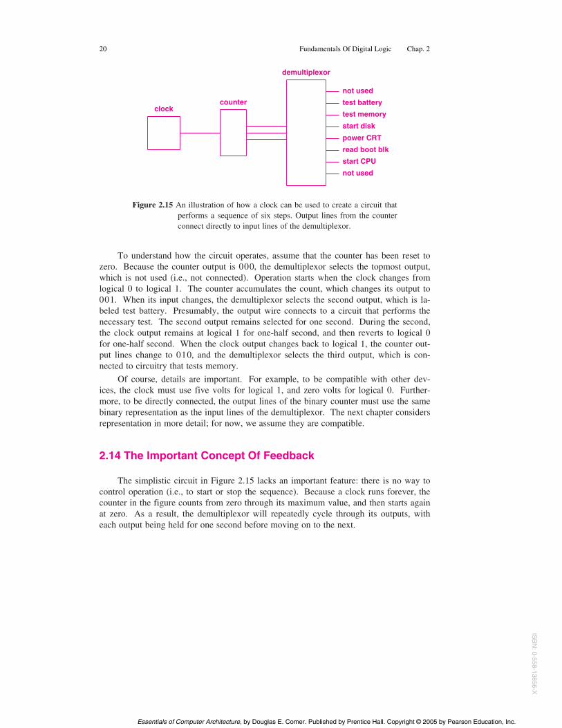
A demultiplexor provides the last piece needed for our simplistic sequencingmechanism — if we combine a clock, counter, and demultiplexor, the resulting circuitcan execute a series of steps. For example, Figure 2.15 shows the interconnection inwhich the output of a clock is used as input to a binary counter, and the output of abinary counter is used as input to a demultiplexor.
ISB
N: 0
-558
-138
56-X
Essentials of Computer Architecture, by Douglas E. Comer. Published by Prentice Hall. Copyright © 2005 by Pearson Education, Inc.
20 Fundamentals Of Digital Logic Chap. 2
clockcounter
demultiplexor
not used
test battery
test memory
start disk
power CRT
read boot blk
start CPU
not used
Figure 2.15 An illustration of how a clock can be used to create a circuit thatperforms a sequence of six steps. Output lines from the counterconnect directly to input lines of the demultiplexor.
To understand how the circuit operates, assume that the counter has been reset tozero. Because the counter output is 000, the demultiplexor selects the topmost output,which is not used (i.e., not connected). Operation starts when the clock changes fromlogical 0 to logical 1. The counter accumulates the count, which changes its output to001. When its input changes, the demultiplexor selects the second output, which is la-beled test battery. Presumably, the output wire connects to a circuit that performs thenecessary test. The second output remains selected for one second. During the second,the clock output remains at logical 1 for one-half second, and then reverts to logical 0for one-half second. When the clock output changes back to logical 1, the counter out-put lines change to 010, and the demultiplexor selects the third output, which is con-nected to circuitry that tests memory.
Of course, details are important. For example, to be compatible with other dev-ices, the clock must use five volts for logical 1, and zero volts for logical 0. Further-more, to be directly connected, the output lines of the binary counter must use the samebinary representation as the input lines of the demultiplexor. The next chapter considersrepresentation in more detail; for now, we assume they are compatible.
2.14 The Important Concept Of Feedback
The simplistic circuit in Figure 2.15 lacks an important feature: there is no way tocontrol operation (i.e., to start or stop the sequence). Because a clock runs forever, thecounter in the figure counts from zero through its maximum value, and then starts againat zero. As a result, the demultiplexor will repeatedly cycle through its outputs, witheach output being held for one second before moving on to the next.
ISB
N: 0-558-13856-X
Essentials of Computer Architecture, by Douglas E. Comer. Published by Prentice Hall. Copyright © 2005 by Pearson Education, Inc.

Sec. 2.14 The Important Concept Of Feedback 21
Few digital circuits perform the same series of steps repeatedly. How can we ar-range to stop the sequence after the six steps have been executed? The solution lies in afundamental concept: feedback. Feedback lies at the heart of complex digital circuitsbecause it allows the results of processing to affect the way a circuit behaves. In thecomputer startup sequence, feedback is needed for each of the steps. If the disk cannotbe started, for example, the boot sector cannot be read from the disk.
To see a trivial example of feedback, consider how we might use the final output,call it F, from the demultiplexor to stop the process. An easy way consists of using thevalue of F to prevent clock pulses from reaching the counter. That is, instead of con-necting the clock output directly to the counter input, we insert logic gates that only al-low the counter pulses to continue when F has the value 0. In terms of Boolean alge-bra, the counter input should be:
CLOCK and (not F)
That is, as long as F is false, the counter input should be equal to the clock; whenF is true, however, the counter input changes to (and remains) zero; Figure 2.16 showshow two inverters and a nand gate can be used to implement the necessary function.
demultiplexor
counterclock
not used
test battery
test memory
start disk
state CRT
read boot blk
start CPU
stopfeedback
these two gates performthe Boolean and function
Figure 2.16 A modification of the circuit in Figure 2.15 that includes feed-back to stop processing after one pass through each output.
The feedback in Figure 2.16 is fairly obvious because there is an explicit physicalconnection between the last output and the combinatorial circuit on the input side. Thefigure also makes it easy to see why feedback mechanisms are sometimes called feed-back loops†.
33333333333333333333333333333333†A feedback loop is also present among the gates used to construct a flip-flop.
ISB
N: 0
-558
-138
56-X
Essentials of Computer Architecture, by Douglas E. Comer. Published by Prentice Hall. Copyright © 2005 by Pearson Education, Inc.

22 Fundamentals Of Digital Logic Chap. 2
2.15 Starting A Sequence
Figure 2.16 shows that it is possible to use feedback to terminate a process. How-ever, the circuit is still incomplete because it does not contain a mechanism that allowsthe sequence to start. Fortunately, adding a starting condition is trivial. To understandwhy, recall that a counter contains a separate input line that resets the count to zero.All that is needed to make our circuit start running is another input (e.g., from a buttonthat a user pushes) connected to the counter reset.
When the user pushes the button, the counter resets to zero, which causes thecounter’s output to become 000. When it receives an input of all zeros, the demulti-plexor turns on the first output, and turns off the last output. When the last output turnsoff, the nand gate allows the clock pulses through, and the counter begins to run.
Although it does indeed start the sequence, allowing a user to reset the counter cancause problems. For example, consider what happens if a user becomes impatient dur-ing the startup sequence and presses the button a second time. Once the counter resets,the sequence starts again from the beginning. In some cases, performing an operationtwice simply wastes time. In other cases, however, repeating an operation causes prob-lems (e.g., some disk drives require that only one command be issued at a time). Thus,a production system uses complex combinatorial logic to prevent a sequence from beinginterrupted or restarted before it completes.
2.16 Iteration In Software Vs. Replication In Hardware
One of the fundamental differences between software and hardware arises from theway software and hardware handle operations that must be applied to a set of items. Insoftware, the fundamental paradigm for handling multiple items consists of iteration —a programmer writes code that repeatedly finds the next item in a set and applies theoperation to the item. That is, because the underlying system can only apply the opera-tion to one item at a time, a programmer must explicitly specify the number of items inthe set and the order in which they are to be processed. Iteration is so essential to pro-gramming that most programming languages provide a compact syntax that allows theprogrammer to express the iteration clearly (e.g., a for loop).
Although hardware can be built to perform iteration, doing so is difficult, and theresulting hardware is clumsy. Instead, the fundamental hardware paradigm for handlingmultiple items consists of replication — a hardware engineer creates multiple copies ofthe underlying gates, and allows each copy to act on one item. For example, supposewe need to compute a Boolean operation on a set of thirty-two Boolean values. Theideal hardware solution consists of replicating the necessary gate thirty-two times, andallowing each instance to operate on one of the thirty-two items. For example, to com-pute the Boolean not of thirty-two values, a hardware designer might use thirty-two in-verters.
ISB
N: 0-558-13856-X
Essentials of Computer Architecture, by Douglas E. Comer. Published by Prentice Hall. Copyright © 2005 by Pearson Education, Inc.

Sec. 2.16 Iteration In Software Vs. Replication In Hardware 23
Replication is difficult for programmers to understand and appreciate because repli-cation is antithetical to good programming — a programmer is taught to avoid duplicat-ing code. In the hardware world, however, replication has two distinct advantages.First, as we mentioned above, replication often makes the resulting hardware moreelegant than hardware that uses iteration because replication avoids the extra hardwareneeded to select an individual item, move it into place, and move the result back.Second, and more important, replication increases performance dramatically. In addi-tion to avoiding the overhead of selecting and moving items, replication allows multipleoperations to be performed simultaneously. For example, thirty-two inverters workingat the same time can invert thirty-two bits in exactly the same amount of time that ittakes one inverter to invert a single bit. To put it another way: thirty-two invertersworking simultaneously are more than thirty-two times faster than a single inverteriteratively solving the same problem. The notion of hardware replication and paralleloperation appears throughout the text; a later chapter explains how parallelism applieson a larger scale.
2.17 Gate And Chip Minimization
We have glossed over many of the underlying engineering details. For example,once they choose a general design and the amount of replication that will be used, en-gineers seek ways to minimize the amount of hardware needed. There are two issues:minimizing gates and minimizing integrated circuits. The first issue involves generalrules of Boolean algebra. For example, consider the Boolean expression:
not (not z)
A circuit to implement the expression consists of two inverters connected together. Ofcourse, we know that two not operations are the identity function, so the expression canbe replaced by z. That is, a pair of directly connected inverters can be removed from acircuit without affecting the result.
As another example of Boolean expression optimization, consider the expression:
x nor (not x)
Either x will have the value 1, or not x will have the value 1, which means the nor func-tion will always produce the same value, a logical 0. Therefore, the entire expressioncan be replaced by the value 0. In terms of a circuit, it would be foolish to use a norgate and an inverter to compute the expression because the two gates will always yieldthe same output. Thus, once an engineer writes a Boolean expression formula, the for-mula can be analyzed to look for instances of subexpressions that can be reduced or el-iminated without changing the result.
Although Boolean formulas can be optimized, further optimization is needed be-cause the overall goal is minimization of integrated circuits. To understand the com-plexity, recall that some integrated circuits contain multiple copies of a given type ofgate. Thus, minimizing the number of Boolean operations may not help if the optimiza-
ISB
N: 0
-558
-138
56-X
Essentials of Computer Architecture, by Douglas E. Comer. Published by Prentice Hall. Copyright © 2005 by Pearson Education, Inc.

24 Fundamentals Of Digital Logic Chap. 2
tion increases the types of gates required. For example, suppose a Boolean expressionrequires four nand gates, and consider an optimization that reduces the requirements tothree gates: two nand gates and a nor gate. Unfortunately, although the total number ofgates is lower, the optimization increases the number of integrated circuits required (be-cause a single integrated circuit contains four nand gates, but two circuits are requiredfor a nand and a nor gate).
2.18 Using Spare Gates
Consider the circuit in Figure 2.16 carefully†. Assuming the clock, counter, anddemultiplexor each require one integrated circuit, how many additional integrated cir-cuits are required? The obvious answer is two: one is needed for the nand gate (e.g., a7400) and another for the two inverters (e.g., a 7404). However, a hardware engineercan implement the circuit with only one additional integrated circuit. To see how, ob-serve that although the 7400 contains four nand gates, only one is needed. How can thespare gates be used? The trick lies in observing that nand of 1 and 0 is 1, and nand of1 and 1 is 0. That is,
1 nand x
is equivalent to:
not x
So, to use a nand gate as an inverter, an engineer simply connects one of the two inputsto five volts.
2.19 Power Distribution And Heat Dissipation
In addition to planning digital circuits that correctly perform the intended functionand minimizing the number of components used, engineers must contend with theunderlying power and cooling requirements. For example, although the diagrams in thischapter only depict the logical inputs and outputs of gates, every gate consumes power.By everyday standards, the amount of power used by a single integrated circuit is insig-nificant. However, because hardware designers tend to use replication instead of itera-tion, complex digital systems contain many circuits. An engineer must calculate the to-tal power required, construct the appropriate power supplies, and plan additional wiringthat carries power to each chip.
The laws of physics dictate that any device that consumes power will generateheat. The amount of heat generated is proportional to the amount of power consumed,so a small integrated circuit generates a small amount of heat. Because a digital systemuses hundreds of circuits that operate in a small, enclosed space, the total heat generatedcan be significant. Unless engineers plan a mechanism to dissipate heat, high tempera-
33333333333333333333333333333333†Figure 2.16 can be found on page 21.
ISB
N: 0-558-13856-X
Essentials of Computer Architecture, by Douglas E. Comer. Published by Prentice Hall. Copyright © 2005 by Pearson Education, Inc.

Sec. 2.19 Power Distribution And Heat Dissipation 25
tures will cause the circuits to fail. For small systems, engineers add holes to thechassis that allow hot air to escape and be replaced by cooler air from the surroundingroom. For intermediate systems, such as personal computers, fans are added to moveair through the system more quickly. For the largest digital systems, cool air is insuffi-cient — a refrigeration system with liquid coolant must be used.
2.20 Timing
Our quick tour of digital logic omits another important aspect that engineers mustconsider: timing. A gate does not act instantly. Instead a gate takes time to settle (i.e.,to change the output once the input changes). In our examples, timing is irrelevant be-cause the clock runs at the incredibly slow rate of 1Hz and all gates settle in less than amicrosecond. Thus, the gates settle long before the clock pulses.
In practice, timing is an essential aspect of engineering because digital circuits aredesigned to operate at high speed. To ensure that a circuit will operate correctly, an en-gineer must calculate the time required for all gates to settle.
Engineers must also calculate the time required to propagate signals throughout anentire system, and must ensure that the system does not fail because of clock skew. Tounderstand clock skew, consider Figure 2.17 that illustrates a circuit board with a clockthat controls three of the integrated circuits in the system.
IC1
IC2
IC3
clock
Figure 2.17 Illustration of three integrated circuits in a digital system that arecontrolled by a single clock. The length of wire between theclock and an integrated circuit determines when a clock signalarrives.
In the figure, the three integrated circuits are physically distributed (presumably,other integrated circuits occupy the remaining space). Unfortunately, a finite time is re-quired for a signal from the clock to reach each of the circuits, and the time is propor-tional to the length of wire between the clock and a given circuit. As a result, the clock
ISB
N: 0
-558
-138
56-X
Essentials of Computer Architecture, by Douglas E. Comer. Published by Prentice Hall. Copyright © 2005 by Pearson Education, Inc.
26 Fundamentals Of Digital Logic Chap. 2
signal will arrive at some of the integrated circuits sooner than it arrives at others. As arule of thumb, a signal requires one nanosecond to propagate across one foot of wire.Thus, for a system that measures eighteen inches across, the clock signal can reach loca-tions near the clock a nanosecond before the signal reaches the farthest location. Obvi-ously, clock skew can cause a problem if parts of the system must operate before otherparts. An engineer needs to calculate the length of each path and design a layout thatavoids the problem of clock skew.
As a consequence of clock skew, engineers seldom use a single global clock tocontrol a large system. Instead, several clocks are used, with each clock controlling onepart of the system. In particular, clocks that run at the highest rates are used in smallphysical areas. Although using multiple clocks avoids the problems of clock skew,multiple clocks introduce another problem, clock synchronization: all clocks must beengineered to coordinate.
2.21 Physical Size And Process Technologies
Most digital circuits are built from integrated circuits (ICs), a technology that per-mits many transistors to be placed on a single silicon chip along with wiring that inter-connects them. The idea is that the components on an IC form a useful circuit.
ICs are often created by using Complementary Metal Oxide Semiconductor(CMOS) technology. Silicon is doped with impurities to give it negative or positiveionization. The resulting substances are known as N-type silicon or P-type silicon.When arranged in layers, N-type and P-type silicon form transistors.
IC manufacturers do not create a single IC at a time. Instead, a manufacturercreates a round wafer that is a few inches in diameter and contains many copies of agiven IC design. Once the wafer has been created, the vendor cuts out the individualchips, and packages each chip in a plastic case along with pins that connect to the chip.
ICs come in a variety of shapes and sizes; some have only eight external connec-tions (i.e., pins), and others have over four hundred†. Some ICs contain dozens oftransistors, others contain millions.
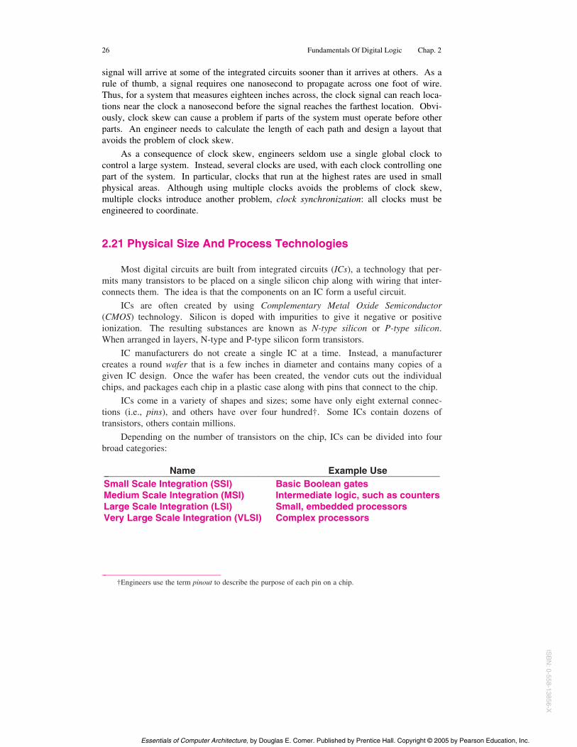
Depending on the number of transistors on the chip, ICs can be divided into fourbroad categories:
Name Example Use222222222222222222222222222222222222222222222222222222222222222222222222Small Scale Integration (SSI) Basic Boolean gatesMedium Scale Integration (MSI) Intermediate logic, such as countersLarge Scale Integration (LSI) Small, embedded processorsVery Large Scale Integration (VLSI) Complex processors
33333333333333333333333333333333†Engineers use the term pinout to describe the purpose of each pin on a chip.
ISB
N: 0-558-13856-X
Essentials of Computer Architecture, by Douglas E. Comer. Published by Prentice Hall. Copyright © 2005 by Pearson Education, Inc.

Sec. 2.21 Physical Size And Process Technologies 27
For example, integrated 7400, 7402, and 7404 circuits described in this chapter are clas-sified as SSI. A binary counter or flip-flop is classified as MSI.
The definition of VLSI keeps changing as manufacturers devise new ways to in-crease the density of transistors per square area. Gordon Moore, a cofounder of IntelCorporation, is attributed with having observed that the density of silicon circuits, meas-ured in the number of transistors per square inch, would double every year. The obser-vation, known as Moore’s Law, was revised in the 1970s, when the rate slowed to dou-bling every eighteen months.
In addition to general-purpose ICs that are designed and sold by vendors, it has be-come possible to build special-purpose ICs. Known as Application Specific IntegratedCircuits (ASICs), the ICs are designed by a private company, and then the designs aresent to a vendor to be manufactured. Although designing an ASIC is expensive andtime-consuming — approximately a million dollars and nearly two years — once thedesign is completed, copies of the ASIC are inexpensive to produce. Thus, high-end di-gital systems often use ASIC chips.
2.22 Circuit Boards And Layers
Most digital systems are built using a printed circuit board that consists of a fiber-glass board with thin metal strips attached to the surface and holes for mounting in-tegrated circuits and other components. In essence, the metal strips on the circuit boardform the wiring that interconnects components.
Can a circuit board be used for complex interconnections that require wires tocross? Interestingly, engineers have developed multilayer circuit boards that solve theproblem. In essence, a multilayer circuit board allows wiring in three dimensions —when a wire must cross another, the designer can arrange to pass the wire up to a higherlayer, make the crossing, and then pass the wire back down.
It may seem that a few layers will suffice for any circuit. However, large complexcircuits with thousands of interconnections may need additional layers. It is not uncom-mon for engineers to design circuit boards that have eighteen layers; the most advancedboards can have twenty-four layers.
2.23 Levels Of Abstraction
As this chapter illustrates, it is possible to view digital logic at various levels ofabstraction. At the lowest level, a transistor is created from silicon. At the next level,multiple transistors are used along with components, such as resistors and diodes, toform gates. At the next level, multiple gates are combined to form intermediate scaleunits, such as flip flops. In later chapters, we will discuss more complex mechanisms,such as processors, memory systems, and I/O devices, that are each constructed frommultiple intermediate scale units. Figure 2.18 summarizes the levels of abstraction.
ISB
N: 0
-558
-138
56-X
Essentials of Computer Architecture, by Douglas E. Comer. Published by Prentice Hall. Copyright © 2005 by Pearson Education, Inc.

28 Fundamentals Of Digital Logic Chap. 2
Abstraction Implemented With22222222222222222222222222222222222222222222222222222222222Computer Circuit board(s)Circuit board Components such as processor and memoryProcessor VLSI chipVLSI chip Many gatesGate Many transistorsTransistor Semiconductor implemented in silicon
Figure 2.18 An example of levels of abstraction in digital logic. An item atone level is implemented using items at the next lower level.
The important point is that moving up the levels of abstraction allows us to hidemore details and talk about larger and larger pieces without giving internal details.When we describe processors, for example, we can consider how a processor workswithout examining the internal structure at the level of gates or transistors.
An important consequence of abstraction arises in the diagrams architects and en-gineers use to describe digital systems. As we have seen, schematic diagrams canrepresent the interconnection of transistors, resistors, and diodes. Diagrams can also beused to represent an interconnection among gates. In later chapters, we will use high-level diagrams that represent the interconnection of processors and memory systems. Insuch diagrams, a small rectangular box will represent a processor or a memory withoutshowing the interconnection of gates. When looking at an architectural diagram, it willbe important to understand the level of abstraction, and to remember that a single itemin a high-level diagram can correspond to an arbitrarily large number of gates.
2.24 Summary
Digital logic refers to the pieces of hardware used to construct digital systems suchas computers. As we have seen, Boolean algebra is an important tool in digital circuitdesign; there is a direct relationship between Boolean functions and the gates used toimplement combinatorial digital circuits. We have also seen that Boolean logic valuescan be described using truth tables.
A clock is a straightforward mechanism that emits pulses at regular intervals. Aclock allows a digital circuit to change without requiring inputs to change, and can beused to provide synchronization among multiple parts of a circuit.
Although we think of digital logic from a mathematical point of view, buildingpractical circuits involves understanding the underlying hardware details. In particular,besides basic correctness, engineers must contend with problems of power distribution,heat dissipation, and clock skew.
ISB
N: 0-558-13856-X
Essentials of Computer Architecture, by Douglas E. Comer. Published by Prentice Hall. Copyright © 2005 by Pearson Education, Inc.