be lab manual
DESCRIPTION
Basic Electronics Lab ManualTRANSCRIPT

L A B O R A T O R Y M A N U A L
Basic Electronics (2110016)
Semester II
Enrollment No. :
Name:
Bachelor of Engineering in
(Electronics & Communication Engineering)
at
Shankersinh Vaghela Bapu Institute of Technology
Gandhinagar

Shankersinh Vaghela Bapu Institute Of Technology
Department of Electronics and Communication Engineering
CERTIFICATE
This is to certify Of class
B.E. Engineering
Enrolment No. has satisfactorily completed his
term work in subject 2110016 – Basic Electronics for the
term ending in June 2014.
Date: ____________
Submitted to: Signature

EC#Department# SVBIT,#Gandhinagar# #pg.$2#
List of Experiments
Sr. Experiment Title Date Sign
1 Introduction to MULTISIM simulation environment and learn how to perform simulations.
2 Perform the following using MULTISIM and verify the operation:
a) Voltage divider circuit b) Current divider circuit
3 Observe the behavior of RLC circuit with ideal voltage source and non-ideal voltage source in MULTISIM.
4 Verify Thevenin’s and Norton’s Theorems using MULTISIM simulator and compare the simulated response with that of the actual circuit.
5
Perform the following using MULTISIM and verify the operation: a) Basic gates OR, AND, NOT realization. b) Prove that NAND and NOR are Universal Gates. c) Implement a Half/Full-Adder Circuit.
6
Perform the following using MULTISIM and verify the operation: a) Realize SR flip-flop using NAND gates. b) Realize D flip-flop using SR flip-flop. c) Realize clocked JK flip-flop using NAND gate.
7 Perform the following using MULTISIM and verify the operation:
a) OPAMP as Inverting Amplifier b) OPAMP as Non-Inverting Amplifier
8 Simulate following signal processing function in MULTISIM:
a) Low-Pass Filter b) High-Pass Filter
9
Case#Studies#Part:I#a) Resistance#Strain#Gauge#b) Automotive#Power:Assisted#Steering#System#c) Microcomputer:controlled#bread#making#machine
10
Case#Studies#Part:II#a) Antinoise#Systems—Noise#Cancellation#b) Global#Positioning#System#c) Digital#Process#Control

EC#Department# SVBIT,#Gandhinagar# #pg.$3#
Experiment 01 AIM: Introduction to MULTISIM simulation environment and learn how to perform simulations. About MULTISIM
It is a schematic capture and simulation program for analog, digital and mixed analog/digital circuits, and is one application program of the National Instruments “Circuit Design Suite”.
The basic steps in modeling and analysis of a digital logic circuit are:
1. Open MULTISIM and create a “design”. 2. Draw a schematic diagram of the circuit (components and interconnections). 3. Define digital test patterns to be applied to the circuit inputs to stimulate the circuit
and connect signal sources to the inputs to produce these patterns. 4. Connect the circuit outputs to one or more indicators to display the response of the
circuit to the test patterns. 5. Run the simulation and examine the results, copying and pasting MULTISIM
windows into lab reports and other documents as needed. 6. Save the design.
Step 1. Open MULTISIM and create a design
MULTISIM is opened from the Start Menu:
Start Menu > All Programs > National Instruments > Circuit Design Suite 11.0 > MULTISIM 11.0 (Version numbers may differ). This creates a blank design called “Design1”, as illustrated in Figure 1. Save the file with the desired design name via menu bar File > Save As to use the standard Windows Save dialog, shown in Figure 2. Navigate to the directory in which you want to save your design, enter the desired file name, and click the Save button. The default file extension for MULTISIM 11.0 design files is .ms11.
Note: A previously created design can be opened via File > Open. In the dialog window, navigate to the directory in which the design is stored, select the file, and click the Open button.

EC#Department# SVBIT,#Gandhinagar# #pg.$4#
Figure 1. Blank design with default name “Design 1”
Figure 2. “File > Save As” dialog window. Design to be saved as file Lab1.ms11
Step 2. Draw a schematic diagram of the circuit

EC#Department# SVBIT,#Gandhinagar# #pg.$5#
• Placing Components
A schematic diagram comprises one or more circuit components, interconnected by wires. Optionally, signal “sources” may be connected to the circuit inputs, and “indicators” to the circuit outputs. Each component is selected from the MULTISIM library and placed on the drawing sheet in the Circuit Window (also called the Workspace). The MULTISIM library is organized into “groups” of related components (Transistors, Diodes, MISC Digital, TTL, etc.). Each group comprises one or more “families”, in which the components are implemented with a common technology. For designing and simulating digital logic circuits, two groups are to be used: “MISC Digital” (TIL family only) and “TTL”.
The “MISC Digital” group has three families of components, of which family “TIL” contains models of generic logic gates, flip-flops, and modular functions. These components are technology-independent, which means that they have only nominal circuit delays and power dissipation, unrelated to any particular technology. Generic components can be used to test the basic functionality of a design, whereas realistic timing information requires the use of technology-specific part models, such as those in the TTL group.
To place a component on the drawing sheet, select it via the Component Browser, which is opened via the component toolbar or the menu bar. From the menu bar, select Place>Component to open the Component Browser window, illustrated in Figure 3. You can also open this window by clicking on the MISC Digital icon in the component toolbar. On the left side of the window, select “Master Database”, group “MISC Digital”, and family “TTL”. The component panel in the center lists all components in the selected family. Scroll down to and click on the desired gate (NAND2 in Figure 3); its symbol and description are displayed on the right side of the window. Then click the OK button. The selected gate will be shown on the drawing sheet next to the cursor; move the cursor to position the gate at the desired location, and then click to fix the position of the component. The component can later be moved to a different location, deleted, rotated, etc. by right clicking on the component and select the desired action. You may also select these operations via the menu bar Edit menu.
After a component has been positioned, the component browser is redisplayed and additional components can be placed by repeating the above actions. When the last component has been placed, click the Close button to close the component selection window. You may return to the component browser at any time to add additional components.
• Drawing Wires
Wires are drawn between component pins to interconnect them. Moving the cursor over a component pin changes the pointer to a crosshair, at which time you may click to initiate a wire from that pin. This causes a wire to appear, connected to the pin and the cursor. Move the cursor to the corresponding pin of the second component (the wire follows the cursor) and click to terminate the wire on that pin. If you do not like the path selected for the wire, you may click at a point on the drawing sheet to fix the wire to that point and then you can move the cursor to continue the wire from that point. You may also initiate or terminate a wire by clicking in the middle of a wire segment, creating a “junction” at that point. This is necessary when a wire is to be fanned out to more than one component input. A partially-wired circuit, including one junction point.
Step 3. Generating test input patterns.
To drive circuit simulations, MULTISIM provides several types of “sources” to generate and apply patterns of logic values to digital circuit inputs. Sources are placed on the schematic sheet and connected to circuit inputs in the same way as circuit components, selecting them from the

EC#Department# SVBIT,#Gandhinagar# #pg.$6#
“Digital_Sources” family of the “Sources” group in the component browser. Note that there is a Place Source shortcut icon in the tool bar.
Step 4. Connect circuit outputs to indicators
To facilitate studying the digital circuit output(s), MULTISIM provides a variety of “indicators”. For digital simulation, the most useful are digital “probes”, hex displays, and the Logic Analyzer instrument.
A logic analyzer is an instrument that captures and displays sequences of digital values over time, with the sequences displayed as waveforms rather than as tables of numbers. The MULTISIM Logic Analyzer instrument can capture and display up to 16 signals. Samples are triggered either by an internal clock (N samples per second) or by an external clock. The logic analyzer must be configured to capture values at the correct sampling times. This is done by clicking on the Set button in the Clock area under the logic analyzer display, opening the Clock Setup window.
Step 5. Run the simulation
A simulation is initiated by pressing the Run (green arrow) button in the toolbar or via the menu bar via Simulate > Run. Alternatively, simulation can be initiated from a Word Generator by pressing the Cycle, Burst, or Step buttons.
You may capture any window and paste it into a Word or other document for generating reports. An individual window is captured by pressing the ALT and Print Screen keys concurrently. You may then “paste” the captured window into a document via the editing features of that document. To capture a circuit diagram in the main window, the simplest method is via the menu bar Tools > Capture Screen Area. This produces a rectangle whose corners can be stretched to include the screen area to be captured; the “copy” icon on the top left corner is pressed to copy the area, which may then be pasted into a document.
Step 6. Save the design and close MULTISIM
The simplest way to save a design is to click the Save icon in the Design Toolbar on the left side of the window, directly above the design name. Alternatively, you may use the standard menu bar File>Save. As mentioned earlier, you should save all designs in a special course directory on either separate drive or on a flash memory device.
MULTISIM is exited as any other Windows program.

EC#Department# SVBIT,#Gandhinagar# #pg.$7#
Experiment 02 AIM: Perform the following using MULTISIM and verify the operation:
a) Voltage divider circuit b) Current divider circuit
Theory: Voltage and Current division allow us to simplify the task of analyzing a circuit.
Voltage Division allows us to calculate what fraction of the total voltage across a series string of resistors is dropped across any one resistor.
Figure 1: Voltage Divider Circuit
For the circuit of Figure 1, Voltage Division formulas are:
!! = !!!!!!!
!! (1)
!! = !!!!!!!
!! (2)
Current Division allows us to calculate what fraction of the total current into a parallel string of resistors flows through any one of the resistors.

EC#Department# SVBIT,#Gandhinagar# #pg.$8#
Figure 2: Current Divider Circuit
For the circuit of Figure 2, Current Division formulas are:
!! = !!!!!!!
!! (3)
!! = !!!!!!!
!! (4)
Procedure:
1. Verifying the voltage division:
a) Construct the circuit as shown in Figure 1. Measure the voltages V1 and V2 by choosing R1 = 5.6kΩ, R2 = 1.2kΩ and setting the variable power supply voltage Vs = 5V. Repeat this step for R1 = R2 = 5.6 KΩ and note down the measurements.
b) Calculate the voltages V1 and V2 by using the formulas (1) and (2) in each case.
c) Compare the results from steps 1a and 1b.
2. Verifying the current division:
a) Construct the circuit as shown in Figure 2. Measure the currents Is, I1 and I2 by choosing R1 = 2.4KΩ, R2 = 5.6 KΩ and Rs =1 KΩ. Set the variable power supply voltage at Vs=10 V. Repeat this step by using R1=R2 =2.4 KΩ and note down the measurements.
b) Calculate the currents I1 and I2 by using the formulas (3) and (4).
c) Compare the results from steps 2a and 2b.
Conclusion: 1) Voltage Division V1= …
V2= …
2) Current Division I1 = …
I2 = …

EC#Department# SVBIT,#Gandhinagar# #pg.$9#
Experiment 03 AIM: Observe the behavior of RLC circuits with ideal and non-ideal voltage sources. Theory:
In Transient Analysis, also called time-domain transient analysis, Multisim computes the circuit’s response as a function of time. This analysis divides the time into segments and calculates the voltage and current levels for each given interval. Finally, the results, voltage versus time, are presented in the Grapher View. Multisim performs Transient Analysis using the following process: 1. Each input cycle is divided into intervals. 2. A DC Operating Point Analysis is performed for each time point in the cycle. 3. The solution for the voltage waveform at a node is determined by the value of that
voltage at each time point over one complete cycle. Assumptions: DC sources have constant values; AC sources have time-dependent values. Capacitors and inductors are represented by energy storage models. Numerical integration is used to calculate the quantity of energy transfer over an interval of time. Running Transient Analysis:
Consider the series RLC circuit shown in Figure 1. According to the theory, the characteristic equation modeling this circuit can be represented as:
Where α is the damping factor and w0 is the natural frequency (or resonant frequency). They are defined by:
The value of the damping factor (α) in relation to the natural frequency (ω0) determines the behavior of the circuit’s response. There are three possible responses: ! α < ω0 : Underdamped response ! α = ω0 : Critically damped response ! α > ω0 : Overdamped response Note that as the value of α increases, the RLC circuit is driven towards an overdamped response. In this example you will use Transient Analysis to plot the step responses of the RLC circuit. Since α depends on the value of the resistance, you will use three different values for R: 40 Ω, 200 Ω and 1 k Ω.

EC#Department# SVBIT,#Gandhinagar# #pg.$10#
Figure 1. Series RLC circuit.
1. Configure the Analysis Parameters as shown in Figure 2. You can reset all the parameters to their default values by clicking the Reset to default button.
Figure 2. Analysis parameters for the Transient Analysis.
4. Select the Output tab.
EC#Department# SVBIT,#Gandhinagar# #pg.$11#
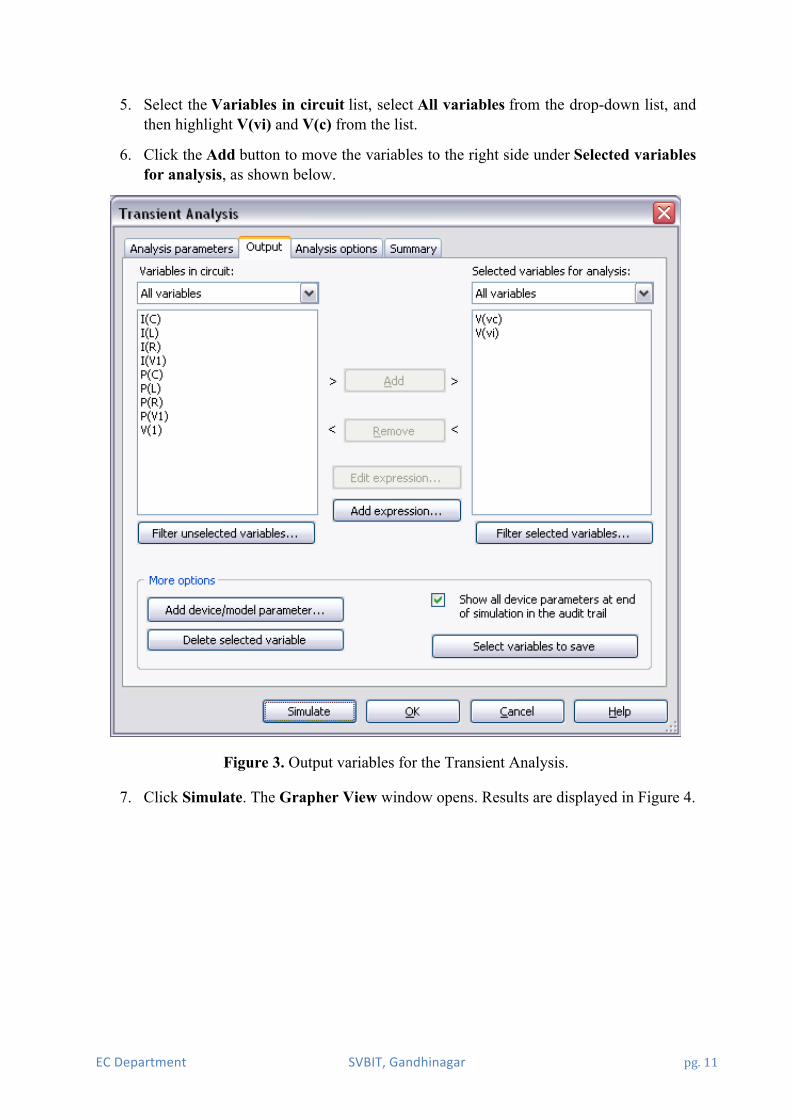
5. Select the Variables in circuit list, select All variables from the drop-down list, and then highlight V(vi) and V(c) from the list.
6. Click the Add button to move the variables to the right side under Selected variables for analysis, as shown below.
Figure 3. Output variables for the Transient Analysis.
7. Click Simulate. The Grapher View window opens. Results are displayed in Figure 4.

EC#Department# SVBIT,#Gandhinagar# #pg.$12#
Figure 4. Transient Analysis results.
As you can see, this is the typical underdamped response of a series RLC circuit.
Note: If you connect the Oscilloscope to the circuit and run the simulation, a similar analysis is performed.
8. Close the Grapher View.
9. Change the value of R to 200 Ω.
10. Run Transient Analysis once again. You will see the critically damped response.
11. Run Transient Analysis for R = 1 kΩ. The overdamped response will be plotted.
In order to compare the three results, merge the plots in one. You can use Overlay Traces from the Graph menu. Figure 5 shows a comparison graph of the results.

EC#Department# SVBIT,#Gandhinagar# #pg.$13#
Figure 5. Step responses of the RLC circuit.
In this example you executed the simulation three times in order to get the step responses of the RLC circuit, however, you can also use Parameter Sweep Analysis to verify the behavior of a circuit when a parameter is varied across a range of values.
Conclusion:

EC#Department# SVBIT,#Gandhinagar# #pg.$14#
Experiment 04 AIM: Verify Thevenin’s and Norton’s Theorems using MULTISIM simulator and compare the simulated response with that of the actual circuit.
THEORY: Thevenin Theorem: Any combination of batteries and resistances with two terminals can be replaced by a single voltage source e and a single series resistor r. The value of e is the open circuit voltage at the terminals, and the value of r is e divided by the current with the terminals short circuited. The Thevenin voltage e is an ideal voltage source equal to the open circuit voltage at the terminals.#
#
Thevenin resistance r is the resistance measured at terminals AB with all voltage sources replaced by short circuits and all current sources replaced by open circuits.
Finally the Load Resistance is put back into the Thevenin’s Equivalent circuit and current through the load resistance in calculated as:
!! =!!"
!! + !!"
Norton theorem:#Any collection of batteries and resistances with two terminals is electrically equivalent to an ideal current source i in parallel with a single resistor r. The value of r is the same as that in the Thevenin equivalent and the current i can be found by dividing the open circuit voltage by r.

EC#Department# SVBIT,#Gandhinagar# #pg.$15#
R1
50Ω
R2100Ω
R3
33Ω
R_L150Ω
V112V
Probe1
'V: '5.55'V'I : '37.0'mA
V_th8V
R_TH
66.33ΩR_L1150Ω
THEVENIN EQ. CIRCUIT
Probe2
'V: '5.55'V'I : '37.0'mA
R_T66.33Ω
R_L2150Ω
I_N120.6mA
NORTON EQ. CIRCUIT
Probe3
'V: '5.55'V'I : '37.0'mA

EC#Department# SVBIT,#Gandhinagar# #pg.$16#
Thevenin’s Observation Table
Sr no. Practical Theoretical
IL VOC IL VOC
Norton’s Observation Table
Sr no. Practical Theoretical
IL ISC IL ISC
Conclusion:

EC#Department# SVBIT,#Gandhinagar# #pg.$17#
Experiment 05 AIM: Perform the following using MULTISIM and verify the operation.
a) Basic gates OR, AND, NOT realization. b) Prove that NAND and NOR are Universal Gates. c) Implement a Half-Adder/Full-Adder Circuit.
a) Basic Gates Realization
Logic gates constitute the foundation blocks for digital logic. Let us start by reviewing these gates and their truth tables:
An AND Gate has two or more inputs and produces one output as follows: output = 1 if all of the inputs are high, output = 0 if one or more of the inputs are low.
An OR gate also has two or more inputs and produces one output as follows: output = 1 if one or more inputs are high, output = 0 if all inputs are low
The inverter gate has one input and produces one output as follows: output =1 if input is low, output = 0 if input is high.
EC#Department# SVBIT,#Gandhinagar# #pg.$18#
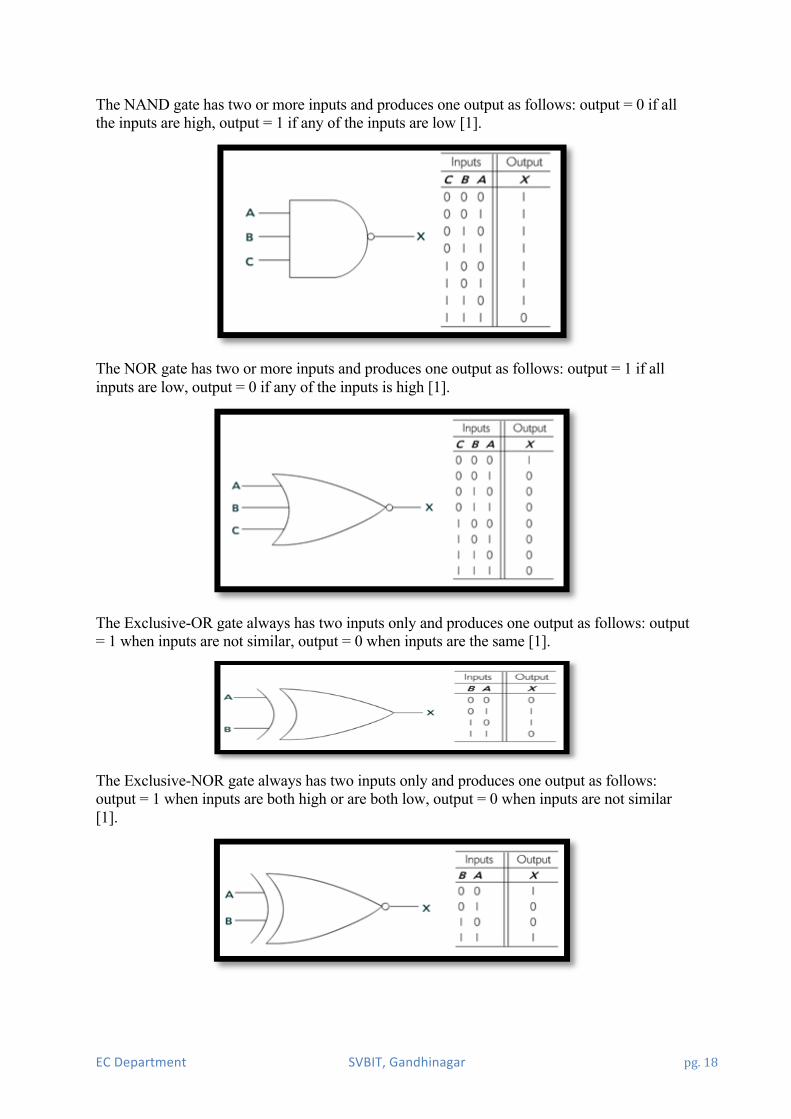
The NAND gate has two or more inputs and produces one output as follows: output = 0 if all the inputs are high, output = 1 if any of the inputs are low [1].
The NOR gate has two or more inputs and produces one output as follows: output = 1 if all inputs are low, output = 0 if any of the inputs is high [1].
The Exclusive-OR gate always has two inputs only and produces one output as follows: output = 1 when inputs are not similar, output = 0 when inputs are the same [1].
The Exclusive-NOR gate always has two inputs only and produces one output as follows: output = 1 when inputs are both high or are both low, output = 0 when inputs are not similar [1].

EC#Department# SVBIT,#Gandhinagar# #pg.$19#
b) NAND as Universal Gate
NOR as Universal Gate
c) Half Adder/Full Adder " Half-Adder: A combinational logic circuit that performs the addition
of two data bits, A and B, is called a half-adder. Addition will result in two output bits; one of which is the sum bit, S, and the other is the carry bit, C. The Boolean functions describing the half-adder are:
# # # S =A ⊕ B C = A B !
0
A U2A
7400N
U2B
7400N
U2C
7400N
U3A
7400N
U3B
7400N
U3C
7400N
1
B
1
C
0
A1
1
B1
A_BAR
B_AND_C
A1_OR_B1
0
A1 U3A
7402N
U3B
7402N
U3C
7402N
U1A
7402N
U1B
7402N
U1C
7402N
1
B1
0
C1
1
A2
1
B2
A_BAR1
B_OR_C1
A2_AND_B2

EC#Department# SVBIT,#Gandhinagar# #pg.$20#
" Full-Adder: The half-adder does not take the carry bit from its previous stage into account. This carry bit from its previous stage is called carry-in bit. A combinational logic circuit that adds two data bits, A and B, and a carry-in bit, Cin , is called a full-adder. The Boolean functions describing the full-adder are: !
S=(x ⊕ y) ⊕ Cin C=xy+Cin(x ⊕ y)
Logic Design Laboratory Manual 7 ___________________________________________________________________________
I. TO REALIZE HALF ADDER TRUTH TABLE BOOLEAN EXPRESSIONS: S=A ! B C=A B i) Basic Gates ii) NAND Gates
II. FULL ADDER TRUTH TABLE BOOLEAN EXPRESSIONS:
S= A ! B ! C C=A B + B Cin + A Cin
i)BASIC GATES
INPUTS OUTPUTS
A B S C
0 0 0 0
0 1 1 0
1 0 1 0
1 1 0 1
INPUTS OUTPUTS
A B Cin S C
0 0 0 0 0
0 0 1 1 0
0 1 0 1 0
0 1 1 0 1
1 0 0 1 0
1 0 1 0 1
1 1 0 0 1
1 1 1 1 1

EC#Department# SVBIT,#Gandhinagar# #pg.$21#
Conclusion:
Logic Design Laboratory Manual 7 ___________________________________________________________________________
I. TO REALIZE HALF ADDER TRUTH TABLE BOOLEAN EXPRESSIONS: S=A ! B C=A B i) Basic Gates ii) NAND Gates
II. FULL ADDER TRUTH TABLE BOOLEAN EXPRESSIONS:
S= A ! B ! C C=A B + B Cin + A Cin
i)BASIC GATES
INPUTS OUTPUTS
A B S C
0 0 0 0
0 1 1 0
1 0 1 0
1 1 0 1
INPUTS OUTPUTS
A B Cin S C
0 0 0 0 0
0 0 1 1 0
0 1 0 1 0
0 1 1 0 1
1 0 0 1 0
1 0 1 0 1
1 1 0 0 1
1 1 1 1 1
Logic Design Laboratory Manual 8 ___________________________________________________________________________
ii) NAND GATES
III. HALF SUBTRACTOR
TRUTH TABLE BOOLEAN EXPRESSIONS: D = A ! B
Br = BA_
INPUTS OUTPUTS
A B D Br
0 0 0 0
0 1 1 1
1 0 1 0
1 1 0 0

EC#Department# SVBIT,#Gandhinagar# #pg.$22#
Experiment 06 AIM: Perform the following:
a) Realize SR flip-flop using NAND gates and verify its operation. b) Realize D flip-flop using SR flip-flop. c) Realize clocked JK flip-flop using NAND gate.
THEORY: A) Realize SR flip-flop using NAND gates and verify its operation.
Logic circuits that incorporate memory cells are called sequential logic circuits; their output depends not only upon the present value of the input but also upon the previous values. Sequential logic circuits often require a timing generator (a clock) for their operation. The latch (flip-flop) is a basic bi-stable memory element widely used in sequential logic circuits. Usually there are two outputs, Q and its complementary value.
An S-R latch consists of two cross-coupled NOR gates. An S-R flip-flop can also be design using cross-coupled NAND gates as shown. The truth tables of the circuits are shown below.
A clocked S-R flip-flop has an additional clock input so that the S and R inputs are active only when the clock is high. When the clock goes low, the state of flip-flop is latched and cannot change until the clock goes high again. Therefore, the clocked S-R flip-flop is also called “enabled” S-R flip-flop.
S" R" QN+1" QN+1_BAR"
0# 0# Qn# Qn_BAR#
0# 1# 0# 1#
1# 0# 1# 0#
1# 1# Not#Defined#
#
SR"FLIP"FLOP"Truth"Table"

EC#Department# SVBIT,#Gandhinagar# #pg.$23#
"
SR"FILP"FLOP"IN"MULTISIM"
#
0
S NAND1A7400N
NAND2B7400N
NOT1A
7404N
NOT2A7404N
1
R
Q
Q_BAR
1
S1 NAND2A7400N
NAND1B7400N
NOT3A
7404N
NOT4A7404N
0
R1
Q1
Q_BAR1
1
S2 NAND3A7400N
NAND4B7400N
NOT5A
7404N
NOT6A7404N
1
R2
Q2
Q_BAR2

EC#Department# SVBIT,#Gandhinagar# #pg.$24#
B) Realize D flip-flop using SR flip-flop:
A D latch combines the S and R inputs of an S-R latch into one input by adding an inverter. When the clock is high, the output follows the D input, and when the clock goes low, the state is latched.
D" QN+1" QN+1_BAR"
0# 0# 1#
1# 1# 0#
D"FLIP"FLOP"TRUTH"TABLE"
#
#
D"FLIP"FLOP"IN"MULTISIM"
0
D NAND1A7400N
NAND2B7400N
NOT1A
7404N
NOT2A7404N
Q
Q_BAR
NOT3A7404N
R
S
1
D1 NAND2A7400N
NAND1B7400N
NOT4A
7404N
NOT5A7404N
Q1
Q_BAR1
NOT6A7404N
R
S

EC#Department# SVBIT,#Gandhinagar# #pg.$25#
C) Realize clocked JK flip-flop using NAND gate.
J" K" QN+1" QN+1_BAR"
0# 0# Qn# Qn_BAR#
0# 1# 0# 1#
1# 0# 1# 0#
1# 1# Qn’# Qn_BAR’#
#
#
1
J NAND1A7400N
NAND2B7400N
0
K
Q
Q_BAR
U1A
7410N
U1B
7410N
CLOCK
0
J1 NAND2A7400N
NAND1B7400N
1
K1
Q1
Q_BAR1
U2A
7410N
U2B
7410N
CLOCK1

EC#Department# SVBIT,#Gandhinagar# #pg.$26#
Experiment 07 AIM: Perform the following:
a) Realize OPAMP Inverting Amplifier b) Realize OPAMP Inverting Amplifier
THEORY:
A) OPAMP as inverting Amplifier
An ideal op-amp by itself is not a very useful device, since any finite non-zero input signal would result in infinite output. (For a real op-amp, the range of the output signal amplitudes is limited by the positive and negative power-supply voltages – referred to as “the rails”.) However, by connecting external components to the ideal op-amp, we can construct useful amplifier circuits.
The triangular block symbol is used to represent an ideal op-amp. The input terminal marked with a “+” (corresponding to V1) is called the non-inverting input; the input terminal marked with a “–” (corresponding to V2) is called the inverting input.
Figure shows basic op-amp circuit, the inverting amplifier. Input signal is applied to the inverting terminal via R1 and the non-inverting terminal is grounded. Let’s derive a relationship between the input voltage Vin and the output voltage Vout. First, since V1 = V2 and V1 is grounded, V2 = 0. Since the current flowing into the inverting input of an ideal op-amp is zero, the current flowing through R1 must be equal in magnitude and opposite in direction to the current flowing through RF (by Kirchhoff’s Current Law):

EC#Department# SVBIT,#Gandhinagar# #pg.$27#
!!"!!!!!!
= !!!"#!!!!!
Since V1 = V2 = 0, we have:
!!"# = −!!!!!!!"
Circuit Diagram In Multisim:
Output:
U2
741
3
2
4
7
6
51
R1
4kΩ
R2
2kΩ
V13 V
VCC12V
VEE-12V
XMM1
XMM2

EC#Department# SVBIT,#Gandhinagar# #pg.$28#
B) Realize OPAMP as non-inverting Amplifier
Figure shows a basic op-amp circuit, the non-inverting amplifier. Input signal is applied to the non-inverting terminal and the inverting terminal is grounded through R1.To understand how the non-inverting amplifier circuit works, we need to derive a relationship between the input voltage Vin and the output voltage Vout. For an ideal op-amp, there is no loading effect at the input, so
V1 = Vin
Since the current flowing into the inverting input of an ideal op-amp is zero, the current flowing through R1 is equal to the current flowing through R2 (by Kirchhoff’s Current Law -- which states that the algebraic sum of currents flowing into a node is zero -- to the inverting input node). We can therefore apply the voltage-divider formula find V1:
!! = !!!!!!!
!!!"#
we know that Vin = V1 = V2, so
Vout = 1+ RFR1
!
"#
$
%&Vin

EC#Department# SVBIT,#Gandhinagar# #pg.$29#
Conclusion:
R14kΩ
R2
2kΩ
U1
741
3
2
4
7
6
51
VCC12V
VEE-12V
XMM1XMM2
V13 V

EC#Department# SVBIT,#Gandhinagar# #pg.$30#
Experiment 08 AIM: Simulate following filtering signal processing function in Multisim:
a) Low-Pass Filter b) High-Pass Filter
Theory: a) Low Pass Filter
U1
741
3
2
47
6
5 1R1
2.2kΩ
R2
10kΩ
R3
10kΩ
R410kΩV1
12V
V212V
C14.7nF
XFG1
XSC2
A B
Ext Trig+
+
_
_ + _
XBP1
IN OUT

EC#Department# SVBIT,#Gandhinagar# #pg.$31#
b) High Pass Filter
Conclusion:
U1
741
3
2
47
6
5 1
R116kΩ
R2
10kΩ
R3
10kΩ
R410kΩV1
12V
V212V
C1
100nF
XFG1
XSC1
A B
Ext Trig+
+
_
_ + _
XBP1
IN OUT

EC#Department# SVBIT,#Gandhinagar# #pg.$32#
Experiment 09 AIM: Case Studies Part-I
Theory:
1. Resistance Strain Gauge: A strain gauge is a device that is bonded to the surface of an object, and whose resistance varies as a function of the surface strain experienced by the object. Strain gauges can be used to measure strain, stress, force, torque, and pressure. The resistance of a conductor with a circular cross-sectional area A, length l, and conductivity σ is given by Equation
! = !σ!!
Depending on the compression or elongation as a consequence of an external force, the length changes, and hence the resistance changes. The relationship between those changes is given by the gauge factor G,
! = !∆! !∆! !
in which the factor ∆!/!, the fractional change in length of an object, is known as the strain. Alternatively, the change in resistance due to an applied strain ε(= ∆!/!)is given by
∆! = !!!" Where R0 is the zero-strain resistance, that is, the resistance of the strain gauge under no strain. A typical gauge has R0=350Ω and G=2. Then for a strain of 1%, the change in resistance is!∆! = 7Ω. A Wheatstone bridge is usually employed to measure the small resistance changes associated with precise strain determination. A typical strain gauge, shown in Figure 9.1, consists of a metal foil (such as nickel–copper alloy) which is formed by a photoetching process in multiple conductors aligned with the direction of the strain to be measured. The conductors are usually bonded to a thin backing made out of a tough flexible plastic. The backing film, in turn, is attached to the test structure by a suitable adhesive.
Figure 9.1. Resistance strain gauge and circuit symbol.
EC#Department# SVBIT,#Gandhinagar# #pg.$33#
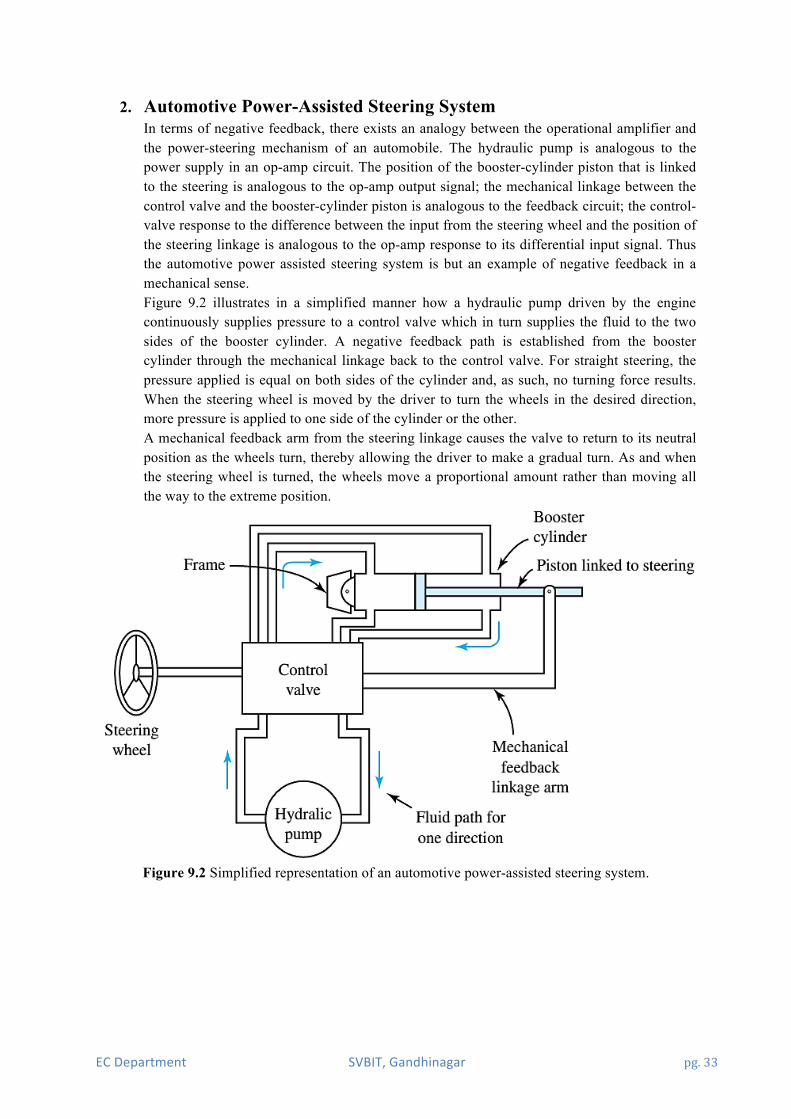
2. Automotive Power-Assisted Steering System In terms of negative feedback, there exists an analogy between the operational amplifier and the power-steering mechanism of an automobile. The hydraulic pump is analogous to the power supply in an op-amp circuit. The position of the booster-cylinder piston that is linked to the steering is analogous to the op-amp output signal; the mechanical linkage between the control valve and the booster-cylinder piston is analogous to the feedback circuit; the control-valve response to the difference between the input from the steering wheel and the position of the steering linkage is analogous to the op-amp response to its differential input signal. Thus the automotive power assisted steering system is but an example of negative feedback in a mechanical sense. Figure 9.2 illustrates in a simplified manner how a hydraulic pump driven by the engine continuously supplies pressure to a control valve which in turn supplies the fluid to the two sides of the booster cylinder. A negative feedback path is established from the booster cylinder through the mechanical linkage back to the control valve. For straight steering, the pressure applied is equal on both sides of the cylinder and, as such, no turning force results. When the steering wheel is moved by the driver to turn the wheels in the desired direction, more pressure is applied to one side of the cylinder or the other. A mechanical feedback arm from the steering linkage causes the valve to return to its neutral position as the wheels turn, thereby allowing the driver to make a gradual turn. As and when the steering wheel is turned, the wheels move a proportional amount rather than moving all the way to the extreme position.
Figure 9.2 Simplified representation of an automotive power-assisted steering system.

EC#Department# SVBIT,#Gandhinagar# #pg.$34#
3. Microcomputer-Controlled Breadmaking Machine Figure 9.3 shows a simplified schematic diagram of a microcomputer-controlled breadmaking machine. A microcomputer along with its timing circuit, keypad, and display unit controls the heating resistor, fan motor, and bread-ingredient mixing motor by means of digitally activated switches. An analog temperature sensor, through an A/D converter, provides the status of temperature to the microcomputer. A digital timer circuit counts down, showing the time remaining in the process. The control programs are stored in ROM and determine when and how long the machine should mix the ingredients added to the bread pan, when and how long the heating resistor should be turned on or off for various parts of the cycle, and when and how long the fan should be on to cool the loaf after baking is finished. The parameters such as light, medium, or dark bread crust are entered through the keypad into RAM. According to the programs stored and the parameters entered, the machine initially mixes the ingredients for several minutes. The heating resistor is turned on to warm the yeast, causing the dough to rise while a temperature of about 90°F is maintained. The time remaining and the temperature are continually checked until the baked loaf is cooled, and the finished bread is finally ready in about 4 hours. Microprocessors and computers in various forms are used extensively in household appliances, automobiles, and industrial equipment.
Figure 9.3 Simplified schematic diagram of a microcomputer-controlled bread making machine.

EC#Department# SVBIT,#Gandhinagar# #pg.$35#
Experiment 10 AIM: Case Studies Part-II
Theory:
1. Antinoise Systems—Noise Cancellation Traditionally sound-absorbing materials have been used quite effectively to reduce noise levels in aircraft, amphitheaters, and other locations. An alternate way is to develop an electronic system that cancels the noise. Ear doctors and engineers have successfully developed ear devices that will nearly eliminate the bothersome and irritating noise (so-called tinnitus) experienced by patients suffering from Meniere’s disease. For passengers in airplanes, helicopters, and other flying equipment, a proper headgear is being developed in order to eliminate the annoying noise. Applications could conceivably extend to people residing near airports and bothered by airplane takeoffs and landings. For industrial workers who are likely to develop long-term ill effects due to various noises they may be subjected to in their workplace, and even for persons who are irritated by the pedestrian noise levels in certain locations, antinoise systems that nearly eliminate or nullify noise become very desirable. Figure 10.1 illustrates in block-diagram form the principle of noise cancellation as applied to an aircraft carrying passengers. The electric signal resulting after sampling the noise at the noise sources is passed through a filter whose transfer function is continuously adjusted by a special-purpose computer to match the transfer function of the sound path. An inverted version of the signal is finally applied to loudspeakers, which project the sound waves out of phase with those from the noise sources, nearly canceling the noise. Microphones on the headrests monitor the sound experienced by the airline passengers so that the computer can determine the proper filter adjustments. Signal processing, which is concerned with manipulating signals to extract information and to use that information to generate other useful electric signals, is indeed an important and far reaching subject.
Figure 10.1 Block diagram of antinoise system to suppress the noise in an aircraft.

EC#Department# SVBIT,#Gandhinagar# #pg.$36#
2. Global Positioning Systems
A global positioning system (GPS) is a modern and sophisticated system in which signals are broadcast from a network of 24 satellites. A receiver, which contains a special-purpose computer to process the received signals and compare their phases, can establish its position quite accurately. Such receivers are used by flyers, boaters, and bikers. Various radio systems that utilize phase relationships among signals received from several radio transmitters have been employed in navigation, surveying, and accurate time determination. An early system of this type, known as LORAN, was developed so that the receivers could determine their latitudes and longitudes. Figure 10.2 illustrates in a simple way the working principle of LORAN, which consists of three transmitters (a master and two slaves) that periodically broadcast 10-cycle pulses of 100-kHz sine waves in a precise phase relationship. The signal received from each transmitter is phase shifted in proportion to the distance from that transmitter to the receiver. A phase reference is established at the receiver by the signal from the master transmitter; then the receiver determines the differential time delay between the master and each of the two slaves. The difference in time delay between the master and a given slave yields a line of position (LOP), as shown in Figure 10.2. If the time delays of the signals from the master and a given slave are equal (i.e., no differential delay), then the line of position is the perpendicular bisector of the line joining the master and that particular slave. On the other hand, if the time delay from the master is smaller by a certain amount, the line of position happens to be a hyperbola situated toward and near the master, as illustrated by LOP for slave 1 in Figure 15.5.1, and LOP for slave 2, where the time delay from slave 2 is smaller. The intersection of the LOPs for the two slaves determines the location of the receiver.
Figure.10.2 Working principle of LORAN.

EC#Department# SVBIT,#Gandhinagar# #pg.$37#
3. Digital Process Control Figure.10.3 shows a block diagram for microcomputer-based control of a physical process, such as a chemical plant. A slight variation of the system can be used for automotive instrumentation in which sensors furnish various signals for speed, fuel reserve, battery voltage, oil pressure, engine temperature, and so on. The data are presented to the driver in one or more displays on the dashboard. In a physical process on the other hand, based on the display information, an operator can assess and direct the operation of the control process through a keyboard or other input devices to the microcomputer. Various physical inputs, such as power and materials, are regulated by actuators, which are in turn controlled by the microcomputer. Electric signals related to the controlled-process parameters, such as pressure and temperature, are produced by various sensors, which in turn#feed the information to the microcomputer. Actuators and sensors may be either analog or digital. Digital-to-analog (D/A) converters are used to convert the digital signals to analog form so as to suit the analog actuators, whereas analog-to-digital (A/D) converters are employed to convert the analog sensor signals to digital form so as to suit the microcomputer. One can think of so many systems in daily practice controlled or monitored by microcomputers. Some examples include monitoring patients in intensive cardiac-care units of hospitals, nuclear-reactor controls, traffic signals, aircraft and automobile instrumentation, chemical plants, and various manufacturing processes.
Figure 10.3 Block diagram for microcomputer-based control of a physical process.