beneficial effects of potassium iodide incorporation on
TRANSCRIPT
RSC Advances
PAPER
Ope
n A
cces
s A
rtic
le. P
ublis
hed
on 1
0 Se
ptem
ber
2019
. Dow
nloa
ded
on 3
/20/
2022
6:1
9:37
PM
. T
his
artic
le is
lice
nsed
und
er a
Cre
ativ
e C
omm
ons
Attr
ibut
ion-
Non
Com
mer
cial
3.0
Unp
orte
d L
icen
ce.
View Article OnlineView Journal | View Issue
Beneficial effects
aInstitute of Solar Energy Materials and D
Engineering, Sichuan University, Chengdu
cn; [email protected]; Fax: +86 28 8bInstitute of New Energy and Low-Carbon T
610027, ChinacChengdu Research Center, Hanergy Thin F
China
† Electronic supplementary information (and incorporated devices; the absolute vfrom the degradation process of control aof control and KI incorporated devices dDOI: 10.1039/c9ra05371a
Cite this: RSC Adv., 2019, 9, 28561
Received 13th July 2019Accepted 26th August 2019
DOI: 10.1039/c9ra05371a
rsc.li/rsc-advances
This journal is © The Royal Society of C
of potassium iodideincorporation on grain boundaries and interfaces ofperovskite solar cells†
Yin Yang,a Lili Wu,*ab Xia Hao, *b Zeguo Tang,c Huagui Lai,a Jingquan Zhang,ab
Wenwu Wanga and Lianghuan Fenga
Grain boundaries and interfacial impurities are the main factors that limit the further development of
polycrystalline perovskite solar cells because their existence severely deteriorates the device
performance. In order to optimize the efficiency of perovskite solar cells, it is essential to eliminate these
defects. In the present work, potassium iodide (KI) is incorporated into the perovskite absorber. KI
incorporation improves the crystallinity of the perovskite, increases the grain size, and decreases the
contact potential distribution at the grain boundary, which are verified by X-ray diffraction, scanning
electronic microscopy and Kelvin probe force microscopy. Besides, the activation energy of the
recombination, estimated from the temperature dependent current–voltage of perovskite solar cells, is
larger than the bandgap calculated from the temperature coefficient. These suggest that KI
incorporation effectively passivates the grain boundaries and interfacial defects. As a result, charge
trapping in the absorber as well as the bimolecular and trap-assisted recombination of the device are
significantly suppressed. Consequently, the open circuit voltage and fill factor of the incorporated
devices are greatly improved, enabling an optimized power conversion efficiency of 19.5%, in
comparison with that of 17.3% for the control one. Our work provides an effective strategy of defect
passivation in perovskite solar cells by KI incorporation and clarifies the mechanism of the performance
optimization of KI incorporated devices.
Introduction
Over the past decade, the efficiency of organic–inorganic halidehybrid perovskite solar cells has increased from 3.8% to over24%. Such rapid development has made them a strongcompetitor in the thin lm solar cell community.1 One of themost important reasons for the wide investigation of perovskitesolar cells is the advantages of the organic–inorganic halidehybrid perovskite material, such as long lifetime and diffusionlength of the carrier,2–4 the tuneable band gap.5 Besides, theinexpensive raw materials and simple preparation processes
evices, College of Materials Science and
610064, China. E-mail: [email protected].
5412542; Tel: +86 28 85412542
echnology, Sichuan University, Chengdu
ilm Power Group Ltd., Chengdu 610200,
ESI) available: J–V curves of ve controlalues of Jsc, Voc, FF and PCE obtainednd KI incorporated devices; JVT curvesuring heating and cooling process. See
hemistry 2019
make it possible to achieve large-scale and cost-effectiveproduction.
The common structure of the organic–inorganic halidehybrid perovskite material is AMX3 (A ¼ methylammonium(MA) CH3NH3
+, or formamidinium (FA) CH3(NH2)2+; M ¼ Pb2+
or Sn2+; X ¼ Cl�, Br� or I�). The solution-processable spincoating is one of the regular techniques for preparing absorberand other functional layers of perovskite solar cells. However,impurities at the grain boundaries (GBs) and interfacial defectsare inevitable. Although GBs are not acting as recombinationcentres, they severely hinder the lateral diffusion of carriers andas a result, degrade the device performance.6 Thus, there havebeen many reports attempting to modify GBs by incorporatingvarious additives into the absorption layer of perovskite solarcells to achieve improvements both in efficiency and in stability.A passivation functional groups contained carboxyl, aminegroups and aromatic structures were customized by Yang et al.,and the loss of open circuit voltage for the perovskite solar cellwas reduced due to the successful elimination of defects in theabsorption layer.7 Niu et al. demonstrated that the trap statesnear the GB can be effectively passivated by semiconductormolecules having Lewis acid functional groups.8 In addition,interfacial defects are generated during the fabrication processof a sandwich-structured perovskite solar cells, they deteriorate
RSC Adv., 2019, 9, 28561–28568 | 28561
RSC Advances Paper
Ope
n A
cces
s A
rtic
le. P
ublis
hed
on 1
0 Se
ptem
ber
2019
. Dow
nloa
ded
on 3
/20/
2022
6:1
9:37
PM
. T
his
artic
le is
lice
nsed
und
er a
Cre
ativ
e C
omm
ons
Attr
ibut
ion-
Non
Com
mer
cial
3.0
Unp
orte
d L
icen
ce.
View Article Online
the device performance due to the increased trap-assistedrecombination probabilities and recombination velocities.The possible strategy could be modifying the contact propertiesbetween the perovskite layer and functional layers by incorpo-rating additives into absorber. Lee et al. added phenethylammonium to the absorption layer to form a quasi-two-dimensional material with a large band gap at the interface,which provided effective interface passivation and an optimizeddevice performance was witnessed.9
Alkali metals such as K,10,11 Rb12,13 and Cs14,15 with small ionicradii are oen used to replace part of the A-site organic ion ofthe perovskite structure and the incorporation of alkali metalsinto perovskites has been proved to be benecial to suppressthe hysteresis effect and improve the stability of perovskite solarcells. It has been conrmed that the incorporating of KI willimprove the overall performance of perovskite solar cells. Theresults of Tang et al. suggested that the band alignment of theperovskite could be modied by KI incorporation, and theelectron transport barrier was then reduced. The hysteresiseffect was therefore eliminated.11 Bu et al. found that KI couldeliminated hysteresis by enhancing conductivity which accel-erated the charge transport and distribution.16
In our work, we investigated the effects of the defects at GBsand interfaces from the point view of charge transportation andrecombination. We found that KI incorporation realized anobvious increase in PCE of perovskite solar cells and the shelflifetime s80 of the unencapsulated devices increased from lessthan 200 hours to over 1000 hours. The Kelvin probe forcemicroscopy (KPFM), steady state/time-resolved photo-luminescence (PL) and temperature-dependent currentdensity–voltage (JVT) measurements were carried out to clarifythe mechanism of performance improvement induced by KIincorporation. The results suggest that the main reason of theseimprovements is the effective GB and interface passivation,which decrease the barrier of charge transport at the GBs ofperovskites and suppress the bimolecular and trap-assistedrecombination of the solar cells. This veries the importanceof GB and interface passivation for optimizing both the powerconversion efficiency and the long-term stability of perovskitesolar cells.
ExperimentDevice fabrication
The structure of the perovskite solar cells in this work is glass/FTO/SnO2/compact-TiO2/mesoporous-TiO2/(FA0.83MA0.17)Pb(I0.83Br0.17)3/spiro-OMeTAD/Au. The FTO-coated glasssubstrates (NSG TEC 12D, with a 12 U ,�1 square resistance)were purchased from Pilkington Group Limited and a 30 nm-thick SnO2 was then sputtered. The substrates were cleaned insequence in an ultrasonic bath with Amway, deionized waterand ethanol. Aer being dried with N2, the substrates werenally treated by UV-ozone for 15 minutes. The titanium dii-sopropoxide diluted in absolute ethanol was used to prepare thecompact-TiO2 (c-TiO2) by spray pyrolysis with N2 as a carrier gason a hot plate at 400 �C. A mesoporous TiO2 (mp-TiO2) layer wasthen deposited by spin coating for 40 s at 4000 rpm with a ramp
28562 | RSC Adv., 2019, 9, 28561–28568
of 2000 rpm s�1 to achieve a 150–200 nm-thick layer, usinga TiO2 particle paste (Dyesol 30 NR-D) diluted in ethanol.
The (FA0.83MA0.17)Pb(I0.83Br0.17)3 lm was formed by one-step spin coating of the mixed perovskite precursor solution.The composition of the perovskite precursor solution was FAI (1M), PbI2 (1.05 M), MABr (0.2 M) and PbBr2 (0.2 M) in a mixedsolvent of anhydrous N,N-dimethylformamide (DMF) anddimethyl sulfoxide (DMSO). The KI incorporated perovskiteswere obtained by adding 1.5 M–KI solution into precursorswithout introducing any other chemicals.
To deposit a perovskite lm, the perovskite precursor solu-tion was transferred to an N2 glove box with a relative humidityless than 10%, and then dropped onto the TiO2-coated FTOsubstrate. The substrate was spun at 1000 rpm and 4000 rpm for10 s and 50 s respectively. 300 mL of chlorobenzene was pouredon the substrate 10 s prior to the end of the program. The as-spun perovskite lm was then annealed on a hot plate at160 �C for 15 minutes. The hole transport layer was spin-coatedon the surface of perovskite layer at 3000 rpm for 30 s bydropping a solution of spiro-OMeTAD in chlorobenzene (72.3mg/1 mL) incorporated by lithium bis(tri-uoromethylsulphonyl)imide (Li-TFSI, Sigma-Aldrich) and 4-tert-butylpyridine (TBP, Sigma-Aldrich). Finally, a 100 nm-thickAu electrode was thermally evaporated via a shadow mask andthe full structure of the solar cell with a typical area of 0.1886cm2 was completed.
Characterization
The X-Ray Diffraction (XRD) was performed on a DX-2600 X-raydiffractometer (Dandong Fangyuan Instrument Company) withCu-Ka radiation (scan range from 10� to 70�). The morphologyof the lm was observed by a eld emission scanning electronmicroscope (Hitachi S-4300). KPFM measurement was per-formed on the surface of the perovskite lms in ambient aircondition, usingMulti Mode 8 AFMwith commercially availableMESP conductive probe coated with Co/Cr. KPFM is used tostudy the spatially resolved imaging of surface contact potentialdifference (CPD). The photovoltaic characteristics weremeasured using a Keithley 2400 Source Meter under simulatedAM 1.5G sunlight (Sun 2000 solar simulator, ABET Technology)with an illumination power density of 100 mA cm�2, which iscalibrated by a GaAs standard cell. The JVT characteristics ofsolar cells were carried out under a simulated AM1.5 sunlight.The light-induced temperature gradient on the sample wasnegligible and the temperature was increased from 300 K to 360K with a step of 5 K. The device was heated by a self-maderesistance heater and the temperature was monitored bya bonded thermocouple (ST-50, PKC, Inc.). The steady statephotoluminescence (PL) and time-resolved photoluminescence(TRPL) of perovskite lms were characterized by the EdinburghInstruments FLS 980 uorescence spectrometer.
Results and discussion
The cell structure is glass/FTO/SnO2/c-TiO2/mp-TiO2/K(FA0.83MA0.17)Pb(I0.83Br0.17)3/spiro-OMeTAD/Au. The volume
This journal is © The Royal Society of Chemistry 2019
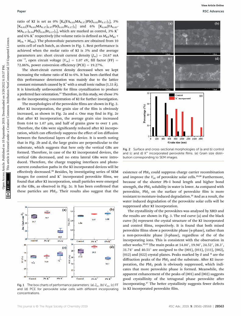
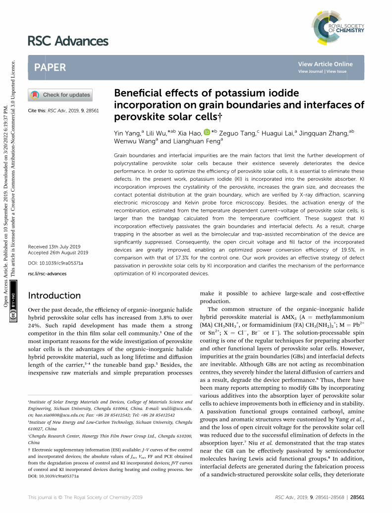
Fig. 2 Surface and cross-sectional morphologies of (a and b) controland (c and d) K+ incorporated perovskite films. (e) Grain size distri-bution corresponding to SEM images.
Paper RSC Advances
Ope
n A
cces
s A
rtic
le. P
ublis
hed
on 1
0 Se
ptem
ber
2019
. Dow
nloa
ded
on 3
/20/
2022
6:1
9:37
PM
. T
his
artic
le is
lice
nsed
und
er a
Cre
ativ
e C
omm
ons
Attr
ibut
ion-
Non
Com
mer
cial
3.0
Unp
orte
d L
icen
ce.
View Article Online
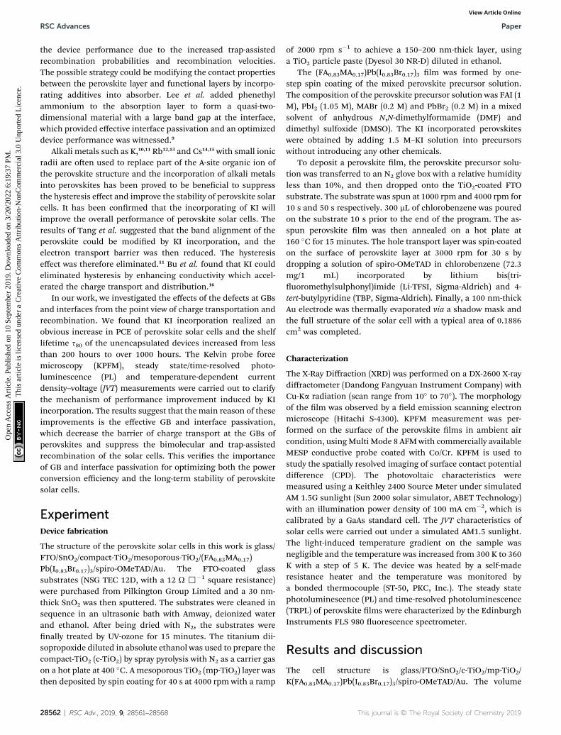
ratio of KI is set as 0% [K0(FA0.83MA0.17)Pb(I0.83Br0.17)3], 3%[K0.03(FA0.83MA0.17)0.97Pb(I0.83Br0.17)3] and 6% [K0.06(FA0.83-MA0.17)0.94Pb(I0.83Br0.17)3], which are marked as control, 3% K+
and 6% K+ respectively (the volume ratio is dened asMKI/MKI +MFA + MMA). The photovoltaic parameters are obtained from 10units cell of each batch, as shown in Fig. 1. Best performance isachieved when the molar ratio of KI is 3% and the averageparameters are: short circuit current density (Jsc) ¼ 24.67 mAcm�2, open circuit voltage (Voc) ¼ 1.07 eV, ll factor (FF) ¼72.86%, power conversion efficiency (PCE) ¼ 19.27%.
The short-circuit current density decreased when we keptincreasing the volume ratio of KI to 6%. It has been claried thatthis performance deterioration was mainly due to the latticeconstantmismatch caused by K+ with a small ionic radius (1.33 A).It is kinetically unfavourable for lms crystallization to producea preferred face orientation.17 Therefore, in this study, we chose 3%as the incorporating concentration of KI for further investigation.
Themorphologies of the perovskite lms are shown in Fig. 2.Aer KI incorporation, the grain size of the lm is obviouslyincreased, as shown in Fig. 2a and c. One may nd in Fig. 2ethat aer KI incorporation, the average grain size increasedfrom 0.64 to 1.07 mm, and half of grains grew to over 1 mm.Therefore, the GBs were signicantly reduced aer KI incorpo-ration, which can effectively suppress the effect of ion diffusionbetween the functional layers of the device. It is worth notingthat in Fig. 2b and d, the large grains are perpendicular to thesubstrate, which suggests that here only the vertical GBs areformed. Therefore, in case of the KI incorporated devices, thevertical GBs decreased, and no extra lateral GBs were intro-duced. Therefore, the charge trapping interfaces and photo-current conduction paths in the KI incorporated devices will beeffectively decreased.18 Besides, by investigating series of SEMimages for control and K+ incorporated perovskite lms, wefound that aer KI incorporation, small particles were emergedat the GBs, as observed in Fig. 2c. It has been conrmed thatthese particles are PbI2. Their results also suggest that the
Fig. 1 The box charts of performance parameters: (a) Jsc, (b) Voc, (c) FFand (d) PCE for perovskite solar cells with different incorporatingconcentrations.
This journal is © The Royal Society of Chemistry 2019
existence of PbI2 could suppress charge carrier recombinationand improve the Voc of perovskite solar cells.19,20 Furthermore,because of the shorter Pb–I bond length and higher bondstrength, the PbI2 solubility in water is lower. As compared withperovskite, PbI2 on the surface of perovskite lm is moreresistant to moisture-induced degradation.21 And as a result, thewater induced degradation of the perovskite solar cells will besuppressed aer KI incorporation.
The crystallinity of the perovskites was analysed by XRD andthe results are shown in Fig. 3. The red curve (a) and the blackcurve (b) represent the crystal structure of the KI incorporatedand control lms, respectively. It is found that both mixedperovskite lms show a perovskite phase (a-phase), rather thana non-perovskite phase (d-phase), regardless of the of theincorporating ions. This is consistent with the observation inother works.22,23 The main peaks at 14.04�, 19.94�, 24.52�, 28.3�,31.74� and 40.51� are assigned to the (001), (011), (111), (002),(012) and (022) crystal planes. Peaks marked by # and * are thediffraction peaks of the PbI2 and the substrate. Aer KI incor-poration, the PbI2 peak is obviously suppressed, which indi-cates that more perovskite phase is formed. Meanwhile, theapparent enhancement of the peaks of (001) and (002) suggestsgood crystallinity of the tetragonal phase perovskite aerincorporating.17 The better crystallinity suggests fewer defectsin KI incorporated perovskite lm.
RSC Adv., 2019, 9, 28561–28568 | 28563
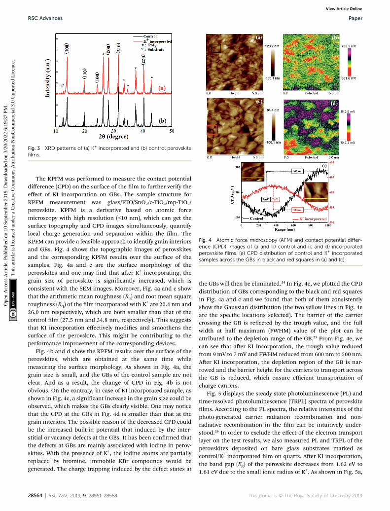
Fig. 3 XRD patterns of (a) K+ incorporated and (b) control perovskitefilms.
Fig. 4 Atomic force microscopy (AFM) and contact potential differ-ence (CPD) images of (a and b) control and (c and d) incorporatedperovskite films. (e) CPD distribution of control and K+ incorporatedsamples across the GBs in black and red squares in (a) and (c).
RSC Advances Paper
Ope
n A
cces
s A
rtic
le. P
ublis
hed
on 1
0 Se
ptem
ber
2019
. Dow
nloa
ded
on 3
/20/
2022
6:1
9:37
PM
. T
his
artic
le is
lice
nsed
und
er a
Cre
ativ
e C
omm
ons
Attr
ibut
ion-
Non
Com
mer
cial
3.0
Unp
orte
d L
icen
ce.
View Article Online
The KPFM was performed to measure the contact potentialdifference (CPD) on the surface of the lm to further verify theeffect of KI incorporation on GBs. The sample structure forKPFM measurement was glass/FTO/SnO2/c-TiO2/mp-TiO2/perovskite. KPFM is a derivative based on atomic forcemicroscopy with high resolution (<10 nm), which can get thesurface topography and CPD images simultaneously, quantifylocal charge generation and separation within the lm. TheKPFM can provide a feasible approach to identify grain interiorsand GBs. Fig. 4 shows the topographic images of perovskitesand the corresponding KPFM results over the surface of thesamples. Fig. 4a and c are the surface morphology of theperovskites and one may nd that aer K+ incorporating, thegrain size of perovskite is signicantly increased, which isconsistent with the SEM images. Moreover, Fig. 4a and c showthat the arithmetic mean roughness (Ra) and root mean squareroughness (Rq) of the lm incorporated with K+ are 20.4 nm and26.0 nm respectively, which are both smaller than that of thecontrol lm (27.5 nm and 34.8 nm, respectively). This suggeststhat KI incorporation effectively modies and smoothens thesurface of the perovskite. This might be contributing to theperformance improvement of the corresponding devices.
Fig. 4b and d show the KPFM results over the surface of theperovskites, which are obtained at the same time whilemeasuring the surface morphology. As shown in Fig. 4a, thegrain size is small, and the GBs of the control sample are notclear. And as a result, the change of CPD in Fig. 4b is notobvious. On the contrary, in case of KI incorporated sample, asshown in Fig. 4c, a signicant increase in the grain size could beobserved, which makes the GBs clearly visible. One may noticethat the CPD at the GBs in Fig. 4d is smaller than that at thegrain interiors. The possible reason of the decreased CPD couldbe the increased built-in potential that induced by the inter-stitial or vacancy defects at the GBs. It has been conrmed thatthe defects at GBs are mainly associated with iodine in perov-skites. With the presence of K+, the iodine atoms are partiallyreplaced by bromine, immobile KBr compounds would begenerated. The charge trapping induced by the defect states at
28564 | RSC Adv., 2019, 9, 28561–28568
the GBs will then be eliminated.24 In Fig. 4e, we plotted the CPDdistribution of GBs corresponding to the black and red squaresin Fig. 4a and c and we found that both of them consistentlyshow the Gaussian distribution (the two yellow lines in Fig. 4eare the specic locations selected). The barrier of the carriercrossing the GB is reected by the trough value, and the fullwidth at half maximum (FWHM) value of the plot can beattributed to the depletion range of the GB.25 From Fig. 4e, wecan see that aer KI incorporation, the trough value reducedfrom 9mV to 7mV and FWHM reduced from 600 nm to 500 nm.Aer KI incorporation, the depletion region of the GB is nar-rowed and the barrier height for the carriers to transport acrossthe GB is reduced, which ensure efficient transportation ofcharge carriers.
Fig. 5 displays the steady state photoluminescence (PL) andtime-resolved photoluminescence (TRPL) spectra of perovskitelms. According to the PL spectra, the relative intensities of thephoto-generated carrier radiation recombination and non-radiative recombination in the lm can be intuitively under-stood.26 In order to exclude the effect of the electron transportlayer on the test results, we also measured PL and TRPL of theperovskites deposited on bare glass substrates marked ascontrol/K+ incorporated lm on quartz. Aer KI incorporation,the band gap (Eg) of the perovskite decreases from 1.62 eV to1.61 eV due to the small ionic radius of K+. As shown in Fig. 5a,
This journal is © The Royal Society of Chemistry 2019
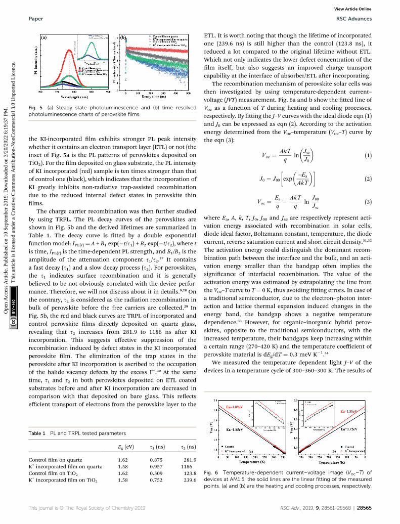
Fig. 5 (a) Steady state photoluminescence and (b) time resolvedphotoluminescence charts of perovskite films.
Paper RSC Advances
Ope
n A
cces
s A
rtic
le. P
ublis
hed
on 1
0 Se
ptem
ber
2019
. Dow
nloa
ded
on 3
/20/
2022
6:1
9:37
PM
. T
his
artic
le is
lice
nsed
und
er a
Cre
ativ
e C
omm
ons
Attr
ibut
ion-
Non
Com
mer
cial
3.0
Unp
orte
d L
icen
ce.
View Article Online
the KI-incorporated lm exhibits stronger PL peak intensitywhether it contains an electron transport layer (ETL) or not (theinset of Fig. 5a is the PL patterns of perovskites deposited onTiO2). For the lm deposited on glass substrate, the PL intensityof KI incorporated (red) sample is ten times stronger than thatof control one (black), which indicates that the incorporation ofKI greatly inhibits non-radiative trap-assisted recombinationdue to the reduced internal defect states in perovskite thinlms.
The charge carrier recombination was then further studiedby using TRPL. The PL decay curves of the perovskites areshown in Fig. 5b and the derived lifetimes are summarized inTable 1. The decay curve is tted by a double exponentialfunction model: IPL(t) ¼ A + B1 exp(�t/s1) + B2 exp(�t/s2), where tis time, IPL(t) is the time-dependent PL strength, and B1/B2 is theamplitude of the attenuation component s1/s2.27 It containsa fast decay (s1) and a slow decay process (s2). For perovskites,the s1 indicates surface recombination and it is generallybelieved to be not obviously correlated with the device perfor-mance. Therefore, we will not discuss about it in details.9,28 Onthe contrary, s2 is considered as the radiation recombination inbulk of perovskite before the free carriers are collected.29 InFig. 5b, the red and black curves are TRPL of incorporated andcontrol perovskite lms directly deposited on quartz glass,revealing that s2 increases from 281.9 to 1186 ns aer KIincorporation. This suggests effective suppression of therecombination induced by defect states in the KI incorporatedperovskite lm. The elimination of the trap states in theperovskite aer KI incorporation is ascribed to the occupationof the halide vacancy defects by the excess I�.30 At the sametime, s1 and s2 in both perovskites deposited on ETL coatedsubstrates before and aer KI incorporation are decreased incomparison with that deposited on bare glass. This reectsefficient transport of electrons from the perovskite layer to the
Table 1 PL and TRPL tested parameters
Eg (eV) s1 (ns) s2 (ns)
Control lm on quartz 1.62 0.875 281.9K+ incorporated lm on quartz 1.58 0.957 1186Control lm on TiO2 1.62 0.509 123.8K+ incorporated lm on TiO2 1.58 0.752 239.6
This journal is © The Royal Society of Chemistry 2019
ETL. It is worth noting that though the lifetime of incorporatedone (239.6 ns) is still higher than the control (123.8 ns), itreduced a lot compared to the original lifetime without ETL.Which not only indicates the lower defect concentration of thelm itself, but also suggests an improved charge transportcapability at the interface of absorber/ETL aer incorporating.
The recombination mechanism of perovskite solar cells wasthen investigated by using temperature-dependent current–voltage (JVT) measurement. Fig. 6a and b show the tted line ofVoc as a function of T during heating and cooling processes,respectively. By tting the J–V curves with the ideal diode eqn (1)and J0 can be expressed as eqn (2). According to the activationenergy determined from the Voc–temperature (Voc–T) curve bythe eqn (3):
Voc ¼ AkT
qln
�Jsc
J0
�(1)
J0 ¼ J00
�exp
��Ea
AkT
��(2)
Voc ¼ Ea
q� AkT
qln
J00
Jsc(3)
where Ea, A, k, T, J0, J00 and Jsc are respectively represent acti-vation energy associated with recombination in solar cells,diode ideal factor, Boltzmann constant, temperature, the diodecurrent, reverse saturation current and short circuit density.31,32
The activation energy could distinguish the dominant recom-bination path between the interface and the bulk, and an acti-vation energy smaller than the bandgap oen implies thesignicance of interfacial recombination. The value of theactivation energy was estimated by extrapolating the line fromthe Voc–T curve to T¼ 0 K, thus avoiding tting errors. In case ofa traditional semiconductor, due to the electron–photon inter-action and lattice thermal expansion induced changes in theenergy band, the bandgap shows a negative temperaturedependence.33 However, for organic–inorganic hybrid perov-skites, opposite to the traditional semiconductors, with theincreased temperature, their bandgaps keep increasing withina certain range (270–420 K) and the temperature coefficient ofperovskite material is dEg/dT ¼ 0.3 meV K�1.34
We measured the temperature dependent light J–V of thedevices in a temperature cycle of 300–360–300 K. The results of
Fig. 6 Temperature-dependent current–voltage image (Voc–T) ofdevices at AM1.5, the solid lines are the linear fitting of the measuredpoints. (a) and (b) are the heating and cooling processes, respectively.
RSC Adv., 2019, 9, 28561–28568 | 28565
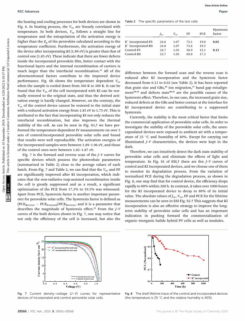
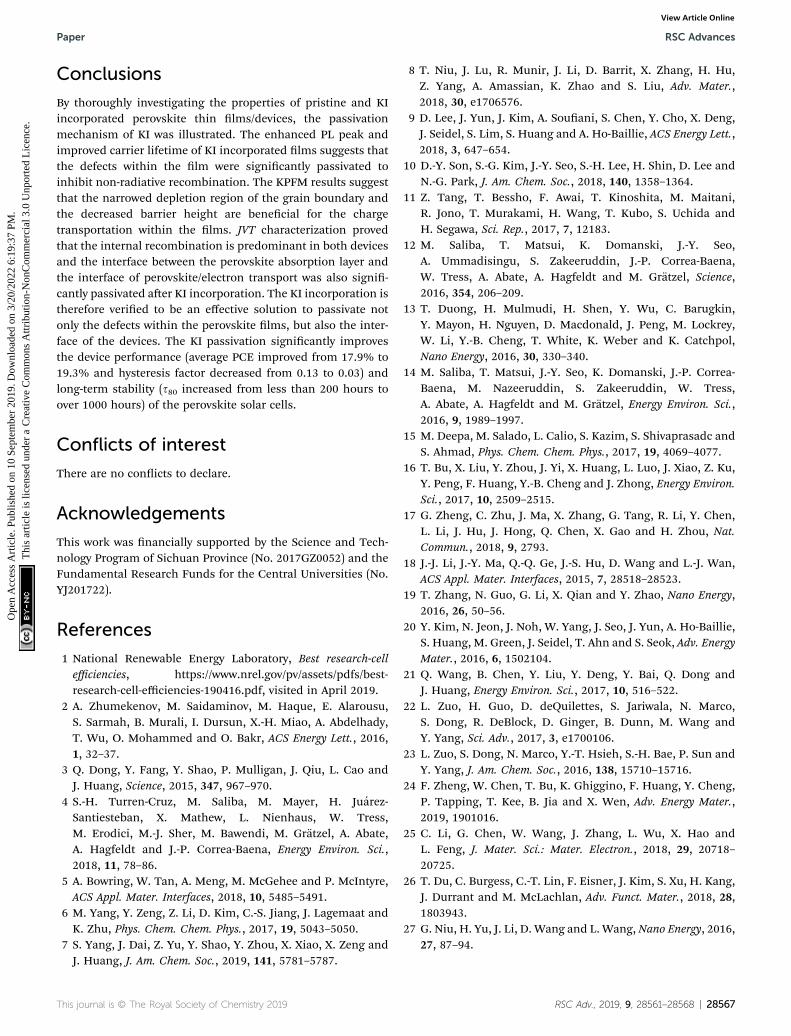
Table 2 The specific parameters of the test cells
Jsc Voc FF PCEHysteresisfactor
K+ incorporated-FS 24.6 1.07 72.1 19.0 0.03K+ incorporated-RS 24.8 1.07 73.6 19.5Control-FS 24.7 1.03 58.9 15.1 0.13Control-RS 23.7 1.05 69.8 17.3
RSC Advances Paper
Ope
n A
cces
s A
rtic
le. P
ublis
hed
on 1
0 Se
ptem
ber
2019
. Dow
nloa
ded
on 3
/20/
2022
6:1
9:37
PM
. T
his
artic
le is
lice
nsed
und
er a
Cre
ativ
e C
omm
ons
Attr
ibut
ion-
Non
Com
mer
cial
3.0
Unp
orte
d L
icen
ce.
View Article Online
the heating and cooling processes for both devices are shown inFig. 6. In heating process, the Voc are linearly correlated withtemperature. In both devices, Voc follows a straight line fortemperature and the extrapolation of the activation energy ishigher than the Eg of the perovskite calculated according to thetemperature coefficient. Furthermore, the activation energy ofthe device aer incorporating KI (1.89 eV) is greater than that ofcontrol one (1.85 eV). These indicate that there are fewer defectsinside the incorporated perovskite lm, better contact with thefunctional layers and the internal recombination of carriers ismuch larger than the interfacial recombination.31 All of theaforementioned factors contribute to the improved deviceperformance. Fig. 6b shows the temperature dependent Vocwhen the sample is cooled down from 360 K to 300 K. It can befound that the Voc of the cell incorporated with KI can be nor-mally restored to the original state, and thus the derived acti-vation energy is hardly changed. However, on the contrary, theVoc of the control device cannot be restored to the initial statewith a reduced activation energy from 1.85 eV to 1.75 eV. This isattributed to the fact that incorporating KI not only reduces theinterfacial recombination, but also improves the thermalstability of the cell. As can be seen in Fig. S3,† we have per-formed the temperature-dependent IV measurements on over 5sets of control/incorporated perovskite solar cells and foundthat results were well reproducible. The activation energies ofthe incorporated samples were between 1.89–1.96 eV, and thoseof the control ones were between 1.82–1.87 eV.
Fig. 7 is the forward and reverse scan of the J–V curves forspecic devices which possess the photovoltaic parameters(summarized in Table 2) close to the average values of eachbatch. From Fig. 7 and Table 2, we can nd that the Voc and FFare signicantly improved aer KI incorporation, which indi-cates that the non-radiative trap-assisted recombination insidethe cell is greatly suppressed and as a result, a signicantoptimization of the PCE from 17.3% to 19.5% was witnessed.Apart from PCE, hysteresis factor is another important param-eter for perovskite solar cells. The hysteresis factor is dened as(PCEReverse � PCEForward)/PCEReverse, and it is a parameter thatdescribes the magnitude of hysteresis effect.35 From the J–Vcurves of the both devices shown in Fig. 7, one may notice thatnot only the efficiency of the cell is increased, but also the
Fig. 7 Current density–voltage (J–V) curves for representativedevices of incorporated and control perovskite solar cells.
28566 | RSC Adv., 2019, 9, 28561–28568
difference between the forward scan and the reverse scan isreduced aer KI incorporation and the hysteresis factordecreased from 0.13 to 0.03 (see Table 2). It has been reportedthat grain size and GBs,36 ion migration,37 band gap misalign-ment38,39 and defects state40,41 are the possible causes of thehysteresis effect. Therefore, in our case, the increased grain size,reduced defects at the GBs and better contact at the interface forKI incorporated device are contributing to a suppressedhysteresis.
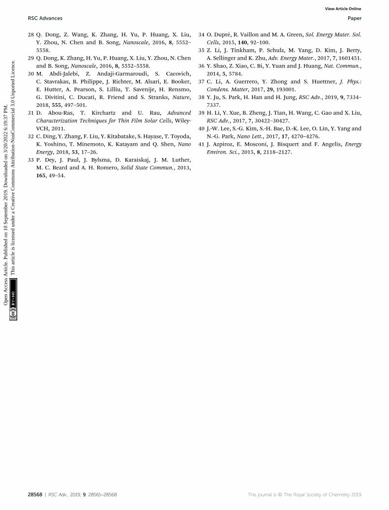
Currently, the stability is the most critical factor that limitsthe commercial application of perovskite solar cells. In order toinvestigate the stability of the perovskite solar cells, the unen-capsulated devices were exposed to ambient air with a temper-ature of 25 �C and humidity of 40%. Except for carrying outilluminated J–V characteristics, the devices were kept in thedark.
Therefore, we can intuitively detect the dark state stability ofperovskite solar cells and eliminate the effects of light andtemperature. In Fig. S1 of ESI,† there are ve J–V curves ofcontrol and KI incorporated devices, and we choose one of themto monitor its degradation process. From the variation ofnormalized PCE during the degradation process, as shown inFig. 8, one may nd that for control device, the efficiency dropsrapidly to 80%within 200 h. In contrast, it takes over 1000 hoursfor the KI incorporated device to decay to 80% of its initialvalue. The absolute values of Jsc, Voc, FF and PCE for the lifetimemeasurements can be seen in ESI Fig. S2.† This suggests that KIincorporation is also an effective strategy to improve the long-term stability of perovskite solar cells and has an importantindication in pushing forward the commercialization oforganic–inorganic halide hybrid PV cells as well as modules.
Fig. 8 The shelf lifetime trace of the control and incorporated devices(the temperature is 25 �C and the relative humidity is 40%).
This journal is © The Royal Society of Chemistry 2019
Paper RSC Advances
Ope
n A
cces
s A
rtic
le. P
ublis
hed
on 1
0 Se
ptem
ber
2019
. Dow
nloa
ded
on 3
/20/
2022
6:1
9:37
PM
. T
his
artic
le is
lice
nsed
und
er a
Cre
ativ
e C
omm
ons
Attr
ibut
ion-
Non
Com
mer
cial
3.0
Unp
orte
d L
icen
ce.
View Article Online
Conclusions
By thoroughly investigating the properties of pristine and KIincorporated perovskite thin lms/devices, the passivationmechanism of KI was illustrated. The enhanced PL peak andimproved carrier lifetime of KI incorporated lms suggests thatthe defects within the lm were signicantly passivated toinhibit non-radiative recombination. The KPFM results suggestthat the narrowed depletion region of the grain boundary andthe decreased barrier height are benecial for the chargetransportation within the lms. JVT characterization provedthat the internal recombination is predominant in both devicesand the interface between the perovskite absorption layer andthe interface of perovskite/electron transport was also signi-cantly passivated aer KI incorporation. The KI incorporation istherefore veried to be an effective solution to passivate notonly the defects within the perovskite lms, but also the inter-face of the devices. The KI passivation signicantly improvesthe device performance (average PCE improved from 17.9% to19.3% and hysteresis factor decreased from 0.13 to 0.03) andlong-term stability (s80 increased from less than 200 hours toover 1000 hours) of the perovskite solar cells.
Conflicts of interest
There are no conicts to declare.
Acknowledgements
This work was nancially supported by the Science and Tech-nology Program of Sichuan Province (No. 2017GZ0052) and theFundamental Research Funds for the Central Universities (No.YJ201722).
References
1 National Renewable Energy Laboratory, Best research-cellefficiencies, https://www.nrel.gov/pv/assets/pdfs/best-research-cell-efficiencies-190416.pdf, visited in April 2019.
2 A. Zhumekenov, M. Saidaminov, M. Haque, E. Alarousu,S. Sarmah, B. Murali, I. Dursun, X.-H. Miao, A. Abdelhady,T. Wu, O. Mohammed and O. Bakr, ACS Energy Lett., 2016,1, 32–37.
3 Q. Dong, Y. Fang, Y. Shao, P. Mulligan, J. Qiu, L. Cao andJ. Huang, Science, 2015, 347, 967–970.
4 S.-H. Turren-Cruz, M. Saliba, M. Mayer, H. Juarez-Santiesteban, X. Mathew, L. Nienhaus, W. Tress,M. Erodici, M.-J. Sher, M. Bawendi, M. Gratzel, A. Abate,A. Hagfeldt and J.-P. Correa-Baena, Energy Environ. Sci.,2018, 11, 78–86.
5 A. Bowring, W. Tan, A. Meng, M. McGehee and P. McIntyre,ACS Appl. Mater. Interfaces, 2018, 10, 5485–5491.
6 M. Yang, Y. Zeng, Z. Li, D. Kim, C.-S. Jiang, J. Lagemaat andK. Zhu, Phys. Chem. Chem. Phys., 2017, 19, 5043–5050.
7 S. Yang, J. Dai, Z. Yu, Y. Shao, Y. Zhou, X. Xiao, X. Zeng andJ. Huang, J. Am. Chem. Soc., 2019, 141, 5781–5787.
This journal is © The Royal Society of Chemistry 2019
8 T. Niu, J. Lu, R. Munir, J. Li, D. Barrit, X. Zhang, H. Hu,Z. Yang, A. Amassian, K. Zhao and S. Liu, Adv. Mater.,2018, 30, e1706576.
9 D. Lee, J. Yun, J. Kim, A. Souani, S. Chen, Y. Cho, X. Deng,J. Seidel, S. Lim, S. Huang and A. Ho-Baillie, ACS Energy Lett.,2018, 3, 647–654.
10 D.-Y. Son, S.-G. Kim, J.-Y. Seo, S.-H. Lee, H. Shin, D. Lee andN.-G. Park, J. Am. Chem. Soc., 2018, 140, 1358–1364.
11 Z. Tang, T. Bessho, F. Awai, T. Kinoshita, M. Maitani,R. Jono, T. Murakami, H. Wang, T. Kubo, S. Uchida andH. Segawa, Sci. Rep., 2017, 7, 12183.
12 M. Saliba, T. Matsui, K. Domanski, J.-Y. Seo,A. Ummadisingu, S. Zakeeruddin, J.-P. Correa-Baena,W. Tress, A. Abate, A. Hagfeldt and M. Gratzel, Science,2016, 354, 206–209.
13 T. Duong, H. Mulmudi, H. Shen, Y. Wu, C. Barugkin,Y. Mayon, H. Nguyen, D. Macdonald, J. Peng, M. Lockrey,W. Li, Y.-B. Cheng, T. White, K. Weber and K. Catchpol,Nano Energy, 2016, 30, 330–340.
14 M. Saliba, T. Matsui, J.-Y. Seo, K. Domanski, J.-P. Correa-Baena, M. Nazeeruddin, S. Zakeeruddin, W. Tress,A. Abate, A. Hagfeldt and M. Gratzel, Energy Environ. Sci.,2016, 9, 1989–1997.
15 M. Deepa, M. Salado, L. Calio, S. Kazim, S. Shivaprasadc andS. Ahmad, Phys. Chem. Chem. Phys., 2017, 19, 4069–4077.
16 T. Bu, X. Liu, Y. Zhou, J. Yi, X. Huang, L. Luo, J. Xiao, Z. Ku,Y. Peng, F. Huang, Y.-B. Cheng and J. Zhong, Energy Environ.Sci., 2017, 10, 2509–2515.
17 G. Zheng, C. Zhu, J. Ma, X. Zhang, G. Tang, R. Li, Y. Chen,L. Li, J. Hu, J. Hong, Q. Chen, X. Gao and H. Zhou, Nat.Commun., 2018, 9, 2793.
18 J.-J. Li, J.-Y. Ma, Q.-Q. Ge, J.-S. Hu, D. Wang and L.-J. Wan,ACS Appl. Mater. Interfaces, 2015, 7, 28518–28523.
19 T. Zhang, N. Guo, G. Li, X. Qian and Y. Zhao, Nano Energy,2016, 26, 50–56.
20 Y. Kim, N. Jeon, J. Noh, W. Yang, J. Seo, J. Yun, A. Ho-Baillie,S. Huang, M. Green, J. Seidel, T. Ahn and S. Seok, Adv. EnergyMater., 2016, 6, 1502104.
21 Q. Wang, B. Chen, Y. Liu, Y. Deng, Y. Bai, Q. Dong andJ. Huang, Energy Environ. Sci., 2017, 10, 516–522.
22 L. Zuo, H. Guo, D. deQuilettes, S. Jariwala, N. Marco,S. Dong, R. DeBlock, D. Ginger, B. Dunn, M. Wang andY. Yang, Sci. Adv., 2017, 3, e1700106.
23 L. Zuo, S. Dong, N. Marco, Y.-T. Hsieh, S.-H. Bae, P. Sun andY. Yang, J. Am. Chem. Soc., 2016, 138, 15710–15716.
24 F. Zheng, W. Chen, T. Bu, K. Ghiggino, F. Huang, Y. Cheng,P. Tapping, T. Kee, B. Jia and X. Wen, Adv. Energy Mater.,2019, 1901016.
25 C. Li, G. Chen, W. Wang, J. Zhang, L. Wu, X. Hao andL. Feng, J. Mater. Sci.: Mater. Electron., 2018, 29, 20718–20725.
26 T. Du, C. Burgess, C.-T. Lin, F. Eisner, J. Kim, S. Xu, H. Kang,J. Durrant and M. McLachlan, Adv. Funct. Mater., 2018, 28,1803943.
27 G. Niu, H. Yu, J. Li, D. Wang and L. Wang, Nano Energy, 2016,27, 87–94.
RSC Adv., 2019, 9, 28561–28568 | 28567
RSC Advances Paper
Ope
n A
cces
s A
rtic
le. P
ublis
hed
on 1
0 Se
ptem
ber
2019
. Dow
nloa
ded
on 3
/20/
2022
6:1
9:37
PM
. T
his
artic
le is
lice
nsed
und
er a
Cre
ativ
e C
omm
ons
Attr
ibut
ion-
Non
Com
mer
cial
3.0
Unp
orte
d L
icen
ce.
View Article Online
28 Q. Dong, Z. Wang, K. Zhang, H. Yu, P. Huang, X. Liu,Y. Zhou, N. Chen and B. Song, Nanoscale, 2016, 8, 5552–5558.
29 Q. Dong, K. Zhang, H. Yu, P. Huang, X. Liu, Y. Zhou, N. Chenand B. Song, Nanoscale, 2016, 8, 5552–5558.
30 M. Abdi-Jalebi, Z. Andaji-Garmaroudi, S. Cacovich,C. Stavrakas, B. Philippe, J. Richter, M. Alsari, E. Booker,E. Hutter, A. Pearson, S. Lilliu, T. Savenije, H. Rensmo,G. Divitini, C. Ducati, R. Friend and S. Stranks, Nature,2018, 555, 497–501.
31 D. Abou-Ras, T. Kirchartz and U. Rau, AdvancedCharacterization Techniques for Thin Film Solar Cells, Wiley-VCH, 2011.
32 C. Ding, Y. Zhang, F. Liu, Y. Kitabatake, S. Hayase, T. Toyoda,K. Yoshino, T. Minemoto, K. Katayam and Q. Shen, NanoEnergy, 2018, 53, 17–26.
33 P. Dey, J. Paul, J. Bylsma, D. Karaiskaj, J. M. Luther,M. C. Beard and A. H. Romero, Solid State Commun., 2013,165, 49–54.
28568 | RSC Adv., 2019, 9, 28561–28568
34 O. Dupre, R. Vaillon and M. A. Green, Sol. Energy Mater. Sol.Cells, 2015, 140, 92–100.
35 Z. Li, J. Tinkham, P. Schulz, M. Yang, D. Kim, J. Berry,A. Sellinger and K. Zhu, Adv. Energy Mater., 2017, 7, 1601451.
36 Y. Shao, Z. Xiao, C. Bi, Y. Yuan and J. Huang, Nat. Commun.,2014, 5, 5784.
37 C. Li, A. Guerrero, Y. Zhong and S. Huettner, J. Phys.:Condens. Matter, 2017, 29, 193001.
38 Y. Ju, S. Park, H. Han and H. Jung, RSC Adv., 2019, 9, 7334–7337.
39 H. Li, Y. Xue, B. Zheng, J. Tian, H. Wang, C. Gao and X. Liu,RSC Adv., 2017, 7, 30422–30427.
40 J.-W. Lee, S.-G. Kim, S.-H. Bae, D.-K. Lee, O. Lin, Y. Yang andN.-G. Park, Nano Lett., 2017, 17, 4270–4276.
41 J. Azpiroz, E. Mosconi, J. Bisquert and F. Angelis, EnergyEnviron. Sci., 2015, 8, 2118–2127.
This journal is © The Royal Society of Chemistry 2019