binary full adder - university of kentucky college of ...elias/projects/12.pdf · 4-bit binary...
TRANSCRIPT

4-Bit Binary AdderEE 584 – Introduction to VLSI
byKiran ArcotAlex Chee
Andrew JenkinsTyler Wells
Table of contents

Introduction......................................................................................................................................3Purpose.............................................................................................................................................3Design.............................................................................................................................................. 3
Circuit Requirements................................................................................................................... 3Block Diagram............................................................................................................................. 3
Description of Individual components.....................................................................................4Schematic Design.........................................................................................................................5
Full Adder................................................................................................................................ 5D-Flip Flop...............................................................................................................................6Shift Register........................................................................................................................... 6Verification Circuit.................................................................................................................. 7
Layout.......................................................................................................................................... 8Functional Verification.................................................................................................................... 9Characterization............................................................................................................................... 9
MOS_plowVT..............................................................................................................................9Par_RC.......................................................................................................................................11Cell_np.......................................................................................................................................11Mos_np...................................................................................................................................... 12
Feasibility of Real World Testing..................................................................................................13Conclusion..................................................................................................................................... 13

IntroductionAn N-bit binary adder is a circuit that upon receiving two N-bit binary numbers, it
computes the summation and returns the aforementioned result as another N-bit binary number.An N-bit adder works by employing a logical building block known as a 1-bit Binary Full Adder.Figure 1 below shows the logical schematic of a 1-bit Binary Full Adder.
Figure 1: 1 bit binary full adder and the truth table1
PurposeThe purpose of this project was to design and implement a 4-bit binary full adder at the
schematic and layout level. This report outlines how both the functionality and the performanceof the adder was characterized using Electronic Design Automation (EDA) software.
Design
Circuit RequirementsThe project itself entailed a few basic requirements. These requirements were that the
circuit could contain a maximum of 12 contact pads and footprint of the circuit had to fit withinthe specified bounding box.
Upon reviewing the basic requirements, it was decided that the Binary full adder wouldreceive inputs sequentially so that the bit width of the adder (number of bits that it could add)could be scaled without increasing the number of input pads. This had the drawback of slowingdown the time it took to complete an add.
It was also decided that a verification circuit would be added to the system so thatcharacterization could be made easy. This verification circuit allowed for a simple check to seeif the adder returned a valid 4-bit result.
1 Image from http://en.wikipedia.org/wiki/Adder_(electronics). Date accessed 11/7/06
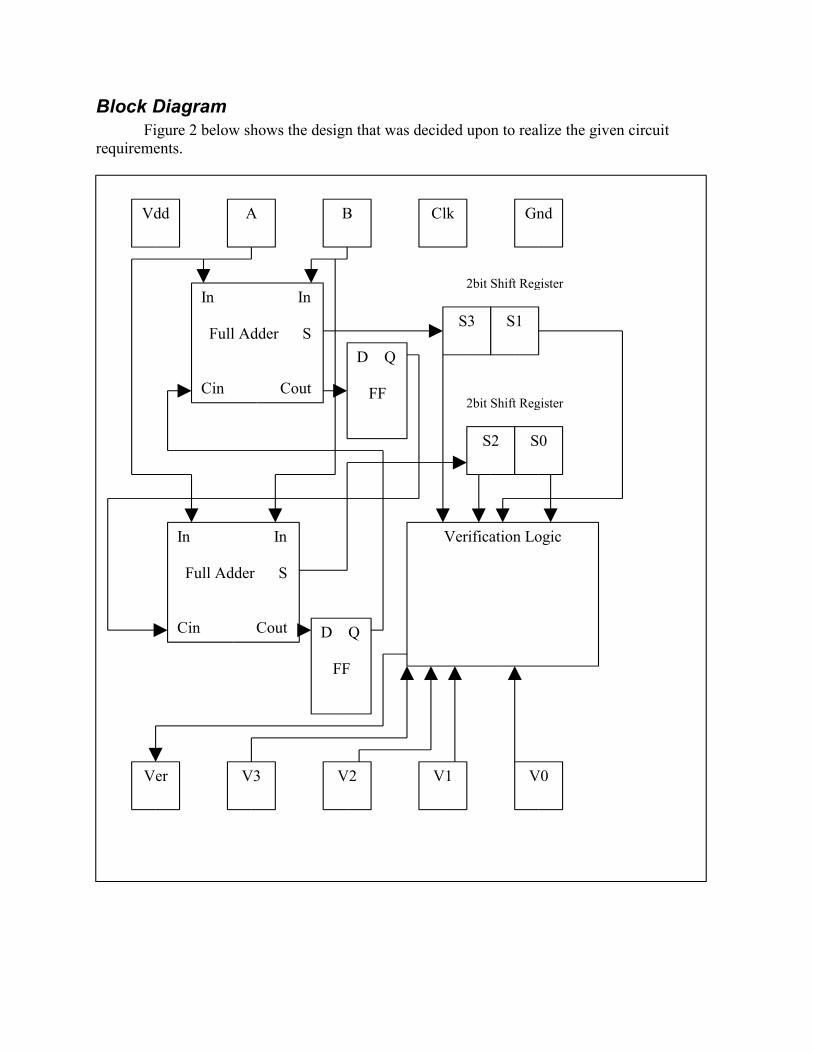
Block DiagramFigure 2 below shows the design that was decided upon to realize the given circuit
requirements.
Vdd A B
In In
Full Adder S
Cin Cout
GndClk
V0Ver V3 V2 V1
D Q
FF
S3 S1
2bit Shift Register
Verification Logic
D Q
FF
In In
Full Adder S
Cin Cout
S2 S0
2bit Shift Register

Description of Individual components
Full AdderThis is the circuit that was described in the introductory section. It receives two one-bit
numbers (plus an optional carry-in) and returns the sum of the two bits and a carry out.
D-Flip FlopA D-Flip flop in this case is implemented using a positive edge triggered Master-Slave D-
FF. Functionally, the D-FF latches whatever D is whenever the clock transitions from low tohigh. It holds this value until the next rising edge of clock.
Shift RegisterA shift register is a bank of D-Flip flops that were strung together such that each time the
first D-flop latches, the previous values of D get shifted to the right (in this design).
Verification CircuitThis circuit takes the output of the adder circuit and compares it with the values V3 – V0.
V3 – V0 is the correct result of the summation applied by tester of the circuit.

Schematic DesignThrough the use of the Cadence2 EDA software, schematic level designs were constructed
for each block in the block diagram listed above. The figures below show each schematic.
Full Adder
2 Cadence is a registered trademark of Cadence Design Systems, Inc, 2655 Seely Avenue, San Jose, CA 95134
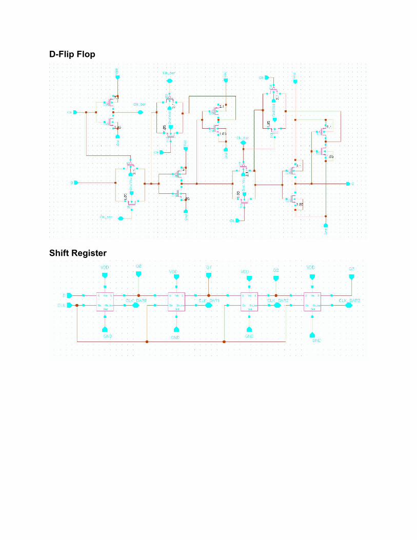
D-Flip Flop
Shift Register
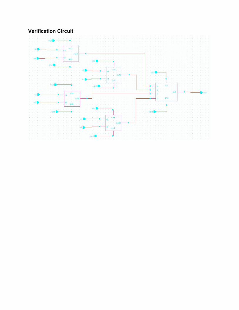
Verification Circuit

Layout--Layout will be finalized and reported at the presentation.
Functional Verification
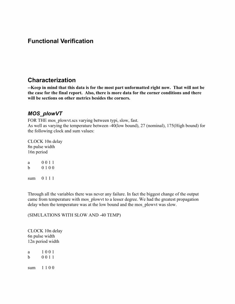
Characterization--Keep in mind that this data is for the most part unformatted right now. That will not bethe case for the final report. Also, there is more data for the corner conditions and therewill be sections on other metrics besides the corners.
MOS_plowVTFOR THE mos_plowvt.scs varying between typi, slow, fast.As well as varying the temperature between -40(low bound), 27 (nominal), 175(High bound) forthe following clock and sum values:
CLOCK 10n delay8n pulse width16n period
a 0 0 1 1b 0 1 0 0
sum 0 1 1 1
Through all the variables there was never any failure. In fact the biggest change of the outputcame from temperature with mos_plowvt to a lesser degree. We had the greatest propagationdelay when the temperature was at the low bound and the mos_plowvt was slow.
(SIMULATIONS WITH SLOW AND -40 TEMP)
CLOCK 10n delay6n pulse width12n period width
a 1 0 0 1b 0 0 1 1
sum 1 1 0 0

Even with the faster period the results of this waveform were similar to that of 16ns periodwaveform. The only difference is the output waveforms are slightly more distorted.
(SIMULATIONS WITH SLOW AND -40 TEMP with 12ns wavefrom)
In conclusion:
mos_plowvt.scs has little effect on the schematic unless the period of the waveform is extremelyfast. The simulation is optimal in the FAST position.

Par_RCTypi_typi
CornerFrequency
Temp 20Mhz 25Mhz 50Mhz 66Mhz 100Mhz155ºC 1 1 1 1 127ºC 1 1 1 1 0-40ºC 1 1 1 0 0
Low_highCorner
Frequency
Temp 20Mhz 25Mhz 50Mhz 66Mhz 100Mhz155ºC 1 1 1 1 127ºC 1 1 1 0 0-40ºC 1 1 1 0 0
High_lowCorner
Frequency
Temp 20Mhz 25Mhz 50Mhz 66Mhz 100Mhz155ºC 1 1 1 1 027ºC 1 1 1 0 0-40ºC 1 1 1 0 0
1’s indicate the summation was correct. 0’s indicate a fail.
Cell_np
Models:par_rc.scs cell_np.scs mos_plowvt.scs mos_np.scstypi_typi typi_typi typi typi_typi
T(°C) F (M Hz) -50 -40 27 155 175
62.5 0 1 1 1 1100 0 1 1 1 1
Models:par_rc.scs cell_np.scs mos_plowvt.scs mos_np.scs

typi_typi slow_slow typi typi_typi
T(°C) F (M Hz) -50 -40 27 155 175
62.5 1 1 1 1 1100 1 1 1 1 1
Models:par_rc.scs cell_np.scs mos_plowvt.scs mos_np.scstypi_typi fast_fast typi typi_typi
Input voltages (a,b) = 1.8 VT(°C)
F (M Hz) -50 -40 27 155 17562.5 0 1 1 1 1100 0 1 1 1 0
Models:par_rc.scs cell_np.scs mos_plowvt.scs mos_np.scstypi_typi fast_fast typi typi_typi
F = 100 MHzT(°C)
Input V-40 27 155 175
1.6 0 0 1 01.65 0 1 1 11.8 0 1 1 12 0 1 1 1
1’s indicate a pass, 0’s indicate a fail

Mos_np
62.5MhzFreq.
Corner
Temp Typi_typi Fast_fast Slow_slow Fast_slow Slow_fast175ºC 1 1 027ºC 1 1 0-40ºC 1 1 0
Slow_slowCorner
Frequency
Temp 6.67Mhz 20Mhz 62.5Mhz175ºC 1 1 0125º 1 1 0100º 1 0 085ºC 1 0 075ºC 1 0 045ºC 0 0 027º 0 0 00ºC 0 0 0
-20ºC 0 0 0-40ºC 0 0 0
1’s indicate a pass, 0’s indicate a fail
Feasibility of Real World Testing--Will be finalized for the presentation.
Conclusion--Will be finalized for the presentation