biogato-docs.its.txstate.edu/jcr:f0e11f8d-e398-498d-ac44...bfraunhofer ipa, nobelstr. 12, 70569...
TRANSCRIPT
BIO: Thomas Ackermann studied chemistry with emphasis on physical chemistry at the University of Würzburg from where he graduated in 2009. After research activities in the field of plasma coatings at the University of Cologne, Mr Ackermann joined the Graduate School of Excellence in advanced Manufacturing Engineering (GSaME) at the University of Stuttgart in 2011. He has recently submitted his PhD thesis. His research project ‘’Cost-efficient production of transparent electrodes based on percolating rodlike nanoparticles’’ has been carried out in cooperation with the Fraunhofer Institute for Manufacturing Engineering and Automation in Stuttgart, where he has worked within multiple public-funded and industrial projects in the field of nanotechnology and manufacturing engineering.
Technical requirements, manufacturing processes and cost
eciency for transparent electrodes based on silver nanowires
and carbon nanotubes
Thomas Ackermanna,b, Serhat Sahakalkanb, Ivica Kolaricb, Engelbert Westkampera andSiegmar Rothc
aGSaME, University of Stuttgart, Nobelstr. 12, 70569 Stuttgart, GermanybFraunhofer IPA, Nobelstr. 12, 70569 Stuttgart, Germany
cSineurop Nanotech GmbH, Munchner Freiheit 6, 80802 Munich, Germany
ABSTRACT
We outline the reasons why indium tin oxide is still not replaced in transparent electrodes although enormousresearch has been carried out in the past decade. We evaluate the advantages and drawbacks of possible alter-native materials with regard to material performance and cost-eciency. As a result, we state that grapheneis a very promising material but the production costs are very high. Without a technological breakthrough to-wards an energy- and material-ecient synthesis of graphene, this material will remain unfeasible for the use inindustrially scaled production of transparent electrodes. Silver nanowires are easier to process but they exhibithigh haze. Within our approach we produce ultra-transparent silver nanowire films and silver nanowire/carbonnanotube hybrid films with low haze. Our manufacturing technique is scalable on conventional smart phoneglass and we present a conceptual production cell for the fabrication of ultra-transparent electrodes with opticaltransmission higher than 97 % and sheet resistance lower than 70 /sq. The optoelectrical performance of thesefilms is superior to most of the recently published silver nanowire films. The theoretical material range for 1 gof AgNWs is 165 m2.
Keywords: Transparent electrodes, silver nanowires, carbon nanotubes, indium replacement, electrical perco-lation, display components, liquid film coating, energy-ecient manufacturing
1. INTRODUCTION
Shorter product life cycles of displays and decreasing prizes of solar cells increased the demand for transparentconductive films (transparent electrodes) within the past years. Transparent electrodes are fundamental compo-nents in displays and touch panels. Emerging markets like flexible electronics do not only increase the demandfor transparent electrodes. Several aspired future devices such as bendable touchscreens require new mechanicalfunctions. Conventional transparent electrodes are made of indium tin oxide (ITO). ITO is a brittle mixedcrystal. Its chemical composition is (In2O3)0.9(ZnO2)0.1. Therefore ITO is often referred to as tin-doped indiumoxide. The existence of a solid material which exhibits both electrical conductivity and optical transparence issomehow contradictory. On the one hand, electrical conductivity demands a delocalized electron gas and on theother hand the electrons absorb photons. The trick of creating a material which is conductive and sucientlytransparent is doping. The presence of tin atoms as n-dopands within an indium oxide lattice structure influencesthe band gap and allows delocalization of the electrons [1, 2, 3]. The optical transmission of ITO is slightly lowerthan of indium oxide.
Although ITO exhibits excellent optoelectrical performance there has been developing a research trend forits replacement. There are both economical and technological drawbacks accompanied with the use of ITO intransparent electrodes. Indium is a rare metal (but not a rare earth metal which is a chemical term) and aby-product from zinc and lead mining. The pure element is produced by an electrolytic process. Due to thesecircumstances the production of indium and hence of ITO is expensive with regard to the material prize. Figure1 illustrates the development of the indium prize during the past decades. The full thin curve represents the
Corresponding author: [email protected]
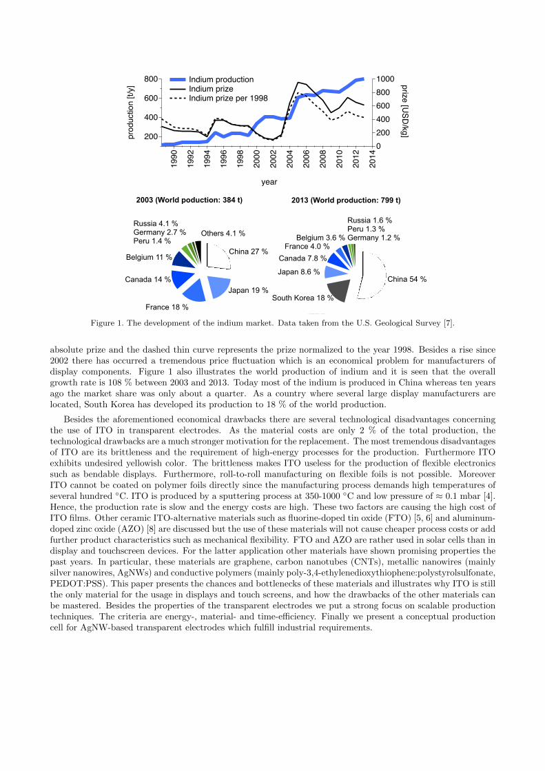
4,1 %1,4 %2,7 %4,1 %
10,8 %
13,5 %
17,6 %
18,9 %
27,0 %
China 27 %
Japan 19 %Canada 14 %
France 18 %
Belgium 11 %
Russia 4.1 %Germany 2.7 %Peru 1.4 %
Others 4.1 %
1,2 %1,3 %1,6 %3,6 %4,0 %
7,8 %
8,6 %
18,0 %
54,0 %China 54 %
South Korea 18 %
Japan 8.6 %
Canada 7.8 %France 4.0 %
Belgium 3.6 %
Russia 1.6 %Peru 1.3 %Germany 1.2 %
2003 (World poduction: 384 t) 2013 (World production: 799 t)
800
600
400
200prod
uctio
n [t/
y]
2014
2012
2010
2008
2006
2004
2002
2000
1998
1996
1994
1992
1990
year
10008006004002000
prize [USD
/kg]
Indium production Indium prize Indium prize per 1998
Figure 1. The development of the indium market. Data taken from the U.S. Geological Survey [7].
absolute prize and the dashed thin curve represents the prize normalized to the year 1998. Besides a rise since2002 there has occurred a tremendous price fluctuation which is an economical problem for manufacturers ofdisplay components. Figure 1 also illustrates the world production of indium and it is seen that the overallgrowth rate is 108 % between 2003 and 2013. Today most of the indium is produced in China whereas ten yearsago the market share was only about a quarter. As a country where several large display manufacturers arelocated, South Korea has developed its production to 18 % of the world production.
Besides the aforementioned economical drawbacks there are several technological disadvantages concerningthe use of ITO in transparent electrodes. As the material costs are only 2 % of the total production, thetechnological drawbacks are a much stronger motivation for the replacement. The most tremendous disadvantagesof ITO are its brittleness and the requirement of high-energy processes for the production. Furthermore ITOexhibits undesired yellowish color. The brittleness makes ITO useless for the production of flexible electronicssuch as bendable displays. Furthermore, roll-to-roll manufacturing on flexible foils is not possible. MoreoverITO cannot be coated on polymer foils directly since the manufacturing process demands high temperatures ofseveral hundred C. ITO is produced by a sputtering process at 350-1000 C and low pressure of 0.1 mbar [4].Hence, the production rate is slow and the energy costs are high. These two factors are causing the high cost ofITO films. Other ceramic ITO-alternative materials such as fluorine-doped tin oxide (FTO) [5, 6] and aluminum-doped zinc oxide (AZO) [8] are discussed but the use of these materials will not cause cheaper process costs or addfurther product characteristics such as mechanical flexibility. FTO and AZO are rather used in solar cells than indisplay and touchscreen devices. For the latter application other materials have shown promising properties thepast years. In particular, these materials are graphene, carbon nanotubes (CNTs), metallic nanowires (mainlysilver nanowires, AgNWs) and conductive polymers (mainly poly-3,4-ethylenedioxythiophene:polystyrolsulfonate,PEDOT:PSS). This paper presents the chances and bottlenecks of these materials and illustrates why ITO is stillthe only material for the usage in displays and touch screens, and how the drawbacks of the other materials canbe mastered. Besides the properties of the transparent electrodes we put a strong focus on scalable productiontechniques. The criteria are energy-, material- and time-eciency. Finally we present a conceptual productioncell for AgNW-based transparent electrodes which fulfill industrial requirements.
2. ALTERNATIVE MATERIALS FOR TRANSPARENT ELECTRODES
2.1 Why ITO is still used in displays and touch panels
As mentioned in the previous section, the major motivations for the replacement of ITO are the creation offurther functions or the implementation of energy-, time- and material-ecient manufacturing processes. Theprize of indium is high but it contributes only 2 % to the overall production costs of ITO-based transparentelectrodes [9]. Hence, alternative materials either have to allow further functionalities like bendabilty or cheapermanufacturing processes.
The principle of electrical conductivity is di↵erent for the aforementioned ITO-alternatives. Graphene andPEDOT:PSS are laminar films like ITO whereas carbon nanotubes and silver nanowires create jackstraw-likepercolating networks based on one-dimensional conductors. It is important to mention that there are two typesof percolation, structural and electrical percolation. Structural percolation represents a continuous physicalpathway along a macroscopic area. Electrical percolation means that the electrons are able to di↵use along thenetwork continuously. Structural percolation is a requirement for electrical percolation (we exclude tunnelinge↵ects) but it does not necessarily cause electrical conduction. The contact resistances of the rods have to besuciently low to allow the electrons to pass from one rod to another. As a result of the di↵erent principles offunction for the electrical conductivity there are di↵erent production methods for graphene, CNT, AgNW andPEDOT-PSS films. Let us go step by step through the alternative materials discussed in literature during thepast decade.
Graphene is a very promising material for several applications in electronics, lightweight construction andbarrier layers. With regard to the application in transparent electrodes, graphene has sparked huge interestsince Wu et al. predicted that a sheet resistance of Rs = 62.4/N /sq is possible, where N is the number ofgraphene layers [10]. The optical transmission is %T = 100 - 2.3N [11]. As of yet, the technologically feasiblesheet resistance is higher and the best value for the sheet resistance is reported by Samsung in cooperationwith several research institutes (Rs = 125 /sq, %T = 97.4) [12]. The industrial requirements for transparentelectrodes are Rs <100 /sq and %T > 90 [13]. Hence, with more layers of graphene the required sheet resistancecan be achieved and the optical transmission is still higher than 90 %. However the manufacturing process ofsuch high-quality graphene is rather inecient. The production of graphene is usually performed by chemicalvapor depostion (CVD) from short hydrocarbons at 1000 C [14]. Moreover, a copper or nickel foil is requiredas substrate since these metals function as a catalyst within the graphene formation. Consequently, besides thatmost of transparent substrates do not resist such high temperatures (exceptions are quartz and sapphire glas),the metal foil cannot be replaced for the process. Direct coating of quartz glas is possible but results in sheetresitance which is higher by orders of magnitude. Moreover, lower temperatures of down to 300 C are possiblewith plasma-enhanced chemical vapor deposition (PE-CVD) on copper foils. However this approach results inhigher sheet resistance than the thermal CVD process. In order the transfer the graphene on a transparentsubstrate, it is coated with a polymer layer. Afterwards the copper is dissolved in a bath of nitric acid andthe graphene-containing carrier polymer is roll-pressed on the final substrate (e.g. a PET foil) and removed bydissolving. The treatment with nitric acid has a further function. It causes p-doping of the graphene whichincreases the conductivity [12]. It is obvious that the high temperatures, the need of oxidizing acids and thelarge-scale consumption of copper is not energy- and material-ecient. Moreover, the coating velocity is ratherlow. Hence, the manufacturing of graphene-based transparent electrodes is not feasible for large-scale production.
Several works report on the liquid-film coating of graphene and CNTs. Thereby the nano carbon materialis dispersed as colloids in a liquid, usually water. After the drying of the liquid the graphene flakes or theCNTs create an electrically percolating network. Compared to CVD-graphene the optoelectrical performance ofdispersion-based graphene films is significantly lower [15]. Dispersion-based CNT films exhibit better optoelec-trical performance than dispersion-based graphene films but underperform compared to CVD-graphene. Mostof the CNT-films do not fulfill the industrial requirements of Rs <100 /sq and %T > 90. CNTs are usuallydispersed in water with a tenside using a tip sonicator. The tenside is needed in order to avoid bundle formation.These tensides reduce the optoelectrical performance due to insolation. They can be removed by treating theCNT films with nitric acid. Additionally it is estimated that the nitric acid causes p-doping of the CNTs as itwas mentioned for graphene previously. Only two publications report on conductivity closely sucient to the
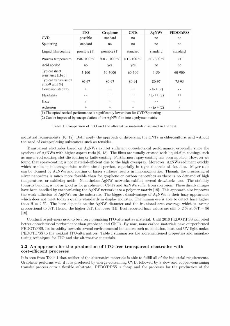
ITO Graphene CNTs AgNWs PEDOT:PSSCVD possible standard no no no
Sputtering standard no no no no
Liquid film coating possible (1) possible (1) standard standard standard
Prozess temperature 350-1000 °C 300 - 1000 °C RT - 100 °C RT - 300 °C RT
Acid needed no yes yes no no
Typical sheet resistance [Ω/sq]
5-100 30-3000 60-300 1-50 60-900
Typical transmission at 550 nm [%]
80-97 80-97 80-91 80-97 75-95
Corrosion stability + ++ ++ - to + (2) - -
Flexibility - - ++ ++ / to ++ (2) ++
Haze / + + - - /
Adhesion + + + - - to + (2) /(1) The optoelectrical performance is significantly lower than for CVD/Sputtering(2) Can be improved by encapsulation of the AgNW film into a polymer matrix
Table 1. Comparison of ITO and the alternative materials discussed in the text.
industrial requirements [16, 17]. Both apply the approach of dispersing the CNTs in chlorosulfuric acid withoutthe need of encapsulating substances such as tensides.
Transparent electrodes based on AgNWs exhibit sucient optoelectrical performance, especially since thesynthesis of AgNWs with higher aspect ratio [9, 18]. The films are usually created with liquid-film coatings suchas mayer-rod coating, slot-die coating or knife-coating. Furthermore spay-coating has been applied. However wefound that spray-coating is not material-ecient due to the high overspray. Moreover, AgNWs sediment quicklywhich results in inhomogeneities within the dispersion, especially in tight channels of slot dies. Mayer-rodscan be clogged by AgNWs and coating of larger surfaces results in inhomogeneities. Though, the processing ofsilver nanowires is much more feasible than for graphene or carbon nanotubes as there is no demand of hightemperatures or oxidizing acids. Nonetheless AgNW networks exhibit several drawbacks too. The stabilitytowards bending is not as good as for graphene or CNTs and AgNWs su↵er from corrosion. These disadvantageshave been handled by encapsulating the AgNW network into a polymer matrix [19]. This approach also improvesthe weak adhesion of AgNWs on the substrate. The biggest disadvantage of AgNWs is their hazy appearancewhich does not meet today’s quality standards in display industry. The human eye is able to detect haze higherthan H = 2 %. The haze depends on the AgNW diameter and the fractional area coverage which is inverseproportional to %T. Hence, the higher %T, the lower %H. Best reported haze values are still > 2 % at %T = 96[18].
Conductive polymers used to be a very promising ITO-alternative material. Until 2010 PEDOT:PSS exhibitedbetter optoelectrical performance than graphene and CNTs. By now, nano carbon materials have outperformedPEDOT:PSS. Its instabilty towards several environmental influences such as oxidation, heat and UV-light makesPEDOT:PSS to the weakest ITO-alternatives. Table 1 summarizes the aforementioned properties and manufac-turing techniques for ITO and the alternative materials.
2.2 An approach for the production of ITO-free transparent electrodes withcost-ecient processes
It is seen from Table 1 that neither of the alternative materials is able to fulfill all of the industrial requirements.Graphene performs well if it is produced by energy-consuming CVD, followed by a slow and copper-consumingtransfer process onto a flexible substrate. PEDOT:PSS is cheap and the processes for the production of the
PEDOT:PSS films are cost-ecient. However it has insucient optoelectrical performance and is unstabletowards environmental influences. The advantages and drawbacks of graphene and PEDOT:PSS are somehowreverse. Graphene exhibits sucient material properties whereas PEDOT:PSS allows cost-ecient processing.However, both of these materials are hard to justify for the replacement of ITO.
There is another inverse trend between two ITO-alternatives. Films made of CNTs are very stable towardscorrosion without a polymer matrix and exhibit haze which is low enough. But su↵er from insucient opto-electrical performance. The optoelectrical performance of AgNW networks can compete with the one of ITObut the haze of the AgNW films is a serious limitation for the use in displays. Despite of these disadvantages,CNTs and AgNWs appear to be the most promising materials for the industrial replacement of ITO, as long aswell-performing graphene can be only produced with inecient processes. This leads to two approaches towardsindustrial use. The first approach is further improvement of the optoelectrical performance of CNT films. Thesecond approach is reducing the haze of AgNW films. As there has been a lot of work published about CNTfilms for transparent electrodes and the best optoelectrical performance was reported in 2011, it seems that CNTfilms have reached their peak with regard to the optimization of conductivity [20]. Furthermore there is stillthe need of acids for best performance. On the other side, the research on AgNW films is more dynamic andthere has been developing a continuous and ongoing improvement of the optoelectrical performance, althoughAgNW networks are already performing very well compared to the other ITO-alternatives. The most importantreason for this development is the availability of AgNWs with high aspect ratio. It is known that the use oflonger AgNWs results in better conductivity since the electrons can di↵use along an AgNW without hitting ona high-resistance junction point for a longer distance in case of long AgNWs. Consequently we decide for thesecond approach and use AgNWs as a material for our transparent electrodes. In order to overcome the problemwith haze we produce ultra-transparent AgNW films, where haze should not be detectable for the human eye.The term ultra-transparent is not clearly defined and means the optical transmission is significantly higher than90 %. Here we refer to films with %T > 97 as ultra-transparent. In case of insucient optoelectrical perfor-mance we add CNTs to the AgNW network. The co-percolation of CNTs within an AgNW network increasesthe conductivity significantly as we have reported previously [33]. As a manufacturing technique we apply asimple dip-coating method. In any case, the AgNWs sediment but it is easier to homogenize a dispersion where asubstrate is dip-coated than doing so for a reservoir which is linked to a meyer-rod or a slot-die device. Moreover,there is no problem with clogging.
3. RESULTS AND DISCUSSION
3.1 Optoelectrical performance of the produced transparent electrodes
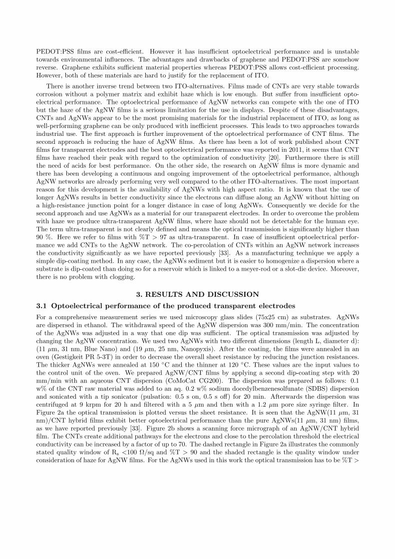
For a comprehensive measurement series we used microscopy glass slides (75x25 cm) as substrates. AgNWsare dispersed in ethanol. The withdrawal speed of the AgNW dispersion was 300 mm/min. The concentrationof the AgNWs was adjusted in a way that one dip was sucient. The optical transmission was adjusted bychanging the AgNW concentration. We used two AgNWs with two di↵erent dimensions (length L, diameter d):(11 µm, 31 nm, Blue Nano) and (19 µm, 25 nm, Nanopyxis). After the coating, the films were annealed in anoven (Gestigkeit PR 5-3T) in order to decrease the overall sheet resistance by reducing the junction resistances.The thicker AgNWs were annealed at 150 C and the thinner at 120 C. These values are the input values tothe control unit of the oven. We prepared AgNW/CNT films by applying a second dip-coating step with 20mm/min with an aqueous CNT dispersion (CoMoCat CG200). The dispersion was prepared as follows: 0.1w% of the CNT raw material was added to an aq. 0.2 w% sodium docedylbenzenesolfunate (SDBS) dispersionand sonicated with a tip sonicator (pulsation: 0.5 s on, 0.5 s o↵) for 20 min. Afterwards the dispersion wascentrifuged at 9 krpm for 20 h and filtered with a 5 µm and then with a 1.2 µm pore size syringe filter. InFigure 2a the optical transmission is plotted versus the sheet resistance. It is seen that the AgNW(11 µm, 31nm)/CNT hybrid films exhibit better optoelectrical performance than the pure AgNWs(11 µm, 31 nm) films,as we have reported previously [33]. Figure 2b shows a scanning force micrograph of an AgNW/CNT hybridfilm. The CNTs create additional pathways for the electrons and close to the percolation threshold the electricalconductivity can be increased by a factor of up to 70. The dashed rectangle in Figure 2a illustrates the commonlystated quality window of Rs <100 /sq and %T > 90 and the shaded rectangle is the quality window underconsideration of haze for AgNW films. For the AgNWs used in this work the optical transmission has to be %T >
AgNW
a) b)
with
draw
al d
irect
ion
102 4 6 8
1002 4 6 8
1000Rs [Ω/sq]
100
95
90
85
80
T[%
]
AgNW(L=19µm,d=25nm),AgNW(L=11µm,d=31 nm)/CNTAgNW(L=11µm,d=31nm)
LiteratureAgNW/CNT or AgNW/Graphene
[21] [22] [23][24], AgNW/Graphene[25], AgNW/GO
AgNW[26] [27][18] [28][29] [30][31] [32]
CNT[16] [17]
CNTs
c)
Figure 2. a) The optoelectrical performance T(Rs) for of the di↵erent AgNW and AgNW/CNT films produced in thiswork compared to values from recent literature. b) Scanning force micrograph of an AgNW/CNT film. c) Laser scanningmicrograph of an AgNW film with very low area coverage.
97 in order to exhibit acceptable haze. As the AgNWs used in this work belong to the thinest AgNWs generally,and haze increases with the AgNW diameter, we expect that AgNW films always have to have transmission inthe ultra-transparent range. It is seen that the pure AgNW(11 µm, 31 nm) networks do not meet the haze-corrected optoelectrical requirement whereas they do after CNTs have been added. However, using the longerAgNWs(19 µm, 25 nm) results in even better optoelectrical performance. Adding CNTs to these AgNWs alsoresults in a decrease of the sheet resistance but only at very low area coverage were both the AgNW and theAgNW/CNT films are significantly outside the quality window. Within and close to the quality window theaddition of CNTs does not influence the optoelectrical performance as it does in case of the shorter AgNWs.Our experiments show that low-haze transparent electrodes with sucient conductivity are possible by usinglong AgNWs without adding further co-percolating materials. Compared to our previous work we do not needto add CNTs in order to achieve sucient optoelectrical performance. With regard to the process eciencythese results are very promising as we do not have the need of a second dip coating step which is slower thanthe coating of AgNWs. We plot several %T(Rs) values from previous works in Figure 2a. We observe that only

our films and the films from Ref. [30] fulfill the haze-corrected industrial requirements. Moreover we observesignificantly better optoelectrical performance for the same AgNWs(19 µm, 25 nm) produced by dip coatingcompared to spray coating by Woo et al., who used AgNWs from the same material supplier [27].
Dip-coating causes anisotropic alignment of the AgNWs. Figure 2c shows a laser scanning micrograph ofAgNWs with L = 19 ± 9 µm and d = 25 ± 5 nm. The sample is aligned along the withdrawal direction of thedip coating process. We found that about 75 % of the AgNWs are aligned rather parallel than orthogonal to thewithdrawal direction (45 to 135 where 90 represents the withdrawal direction). For random percolation thisvalue is 50 %. The image in Figure 2c is a micrograph of a sample with very low area density to allow visibleevidence for anisotropic structural percolation. In order to evaluate whether or not the anisotropic structuralpercolation induces anisotropic electrical percolation we measured the sheet resistance of the films parallel andorthogonal to the withdrawal direction. Anistropy of electrical percolation is not observed for samples with %T= 98.0. It starts to set on at %T = 98.5 where Rs(orthogonal)/Rs(parallel) 1.3. Such a di↵erence is stillacceptable but for %T > 99.0 the ratio increases up to 30. For %T = 98.0 a sheet resistance of Rs 70-150/sq can be achieved. For %T = 97.5 a sheet resistance of Rs 55-75 /sq is possible. These values are withinthe quality window of sucient haze and structural anisotropy does not cause electrical anisostropy. For %T =98 the haze is %H 1.5 on microscopy slides. The bare substrates exhibit haze of %H 0.5.
3.2 Conceptual design of a production cell for transparent electrodes based on silvernanowires
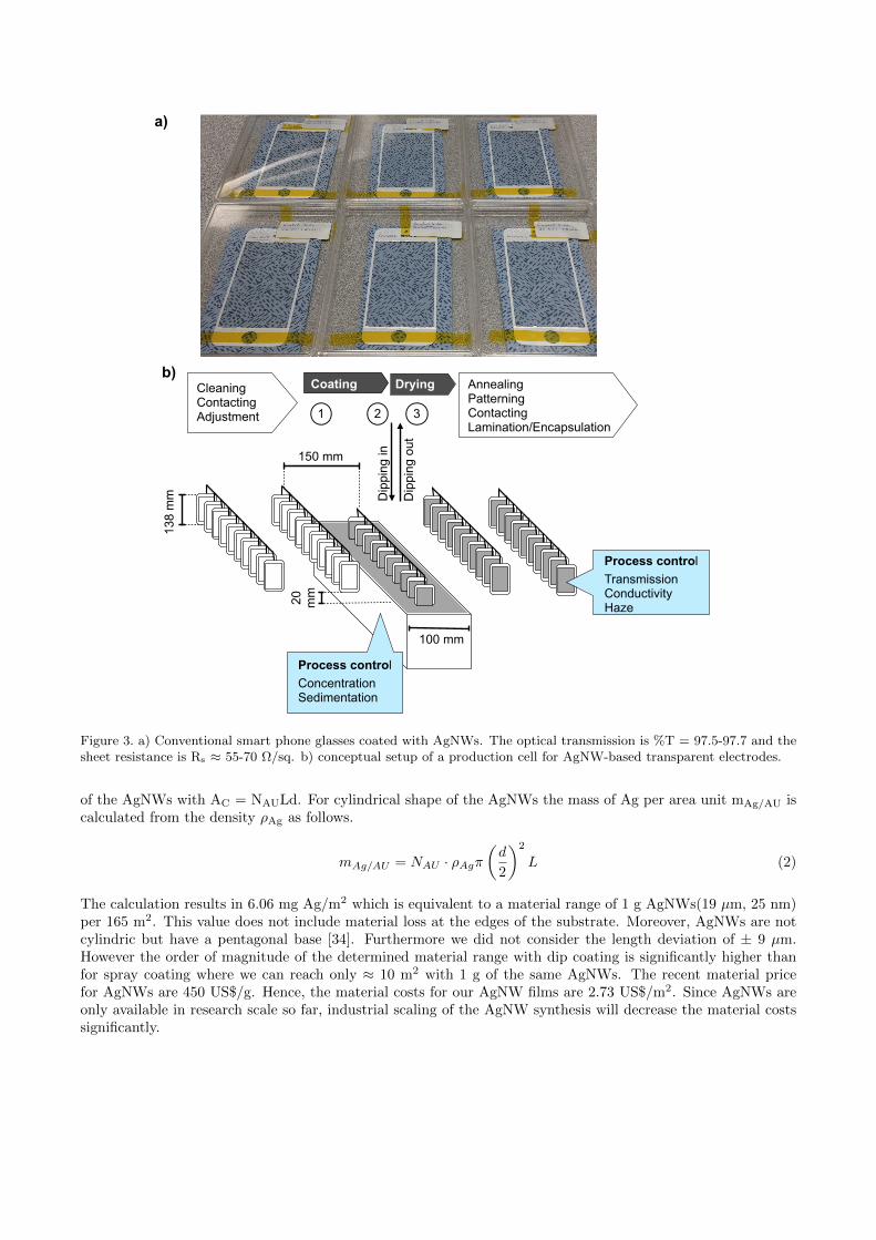
We scaled the dip coating process on commercial smart phone glass and found the film homogeneity to besucient. The optoelectrical performance and film homogeneity is reproducible for withdrawal speeds between150 and 1000 mm/min. The coating time and the drying time are opposed because higher withdrawal speedsresult in thicker liquid films which dry slower. Figure 3a shows six commercial smart phone cover glasses coatedwith AgNWs from this work. The optical transmission is %T = 97.5-97.7 and the sheet resistance is Rs 55-70 /sq. Figure 3b illustrates a conceptual production cell for the coating of smartphone cover glass with ourapproach. Ten substrates are coated simultaneously into a dispersion with a volume of 3750 ml (250x10x15 mm).The AgNW (L = 19 ± 9 µm and d = 25 ± 5 nm) concentration is 0.25 w%. One dip results with withdrawalspeed of 300 mm/min in an optoelectrical performance of %T(Rs) = 97.5(55 /sq). The coating process consistsof three sub processes: (1) positioning, (2) dipping in and (3) dipping out. The velocity of steps (1) and (2) donot have a direct influence of the coating process, step (1) has to be chosen with regard to previous steps suchas adjustment of the substrates and step (2) should not cause waves on the liquid surface. For the velocities (1)1000 mm/min, (2) 1000 mm/min and (3) 300 mm/min we calculated a production rate of 17,000 substratesper 24 h. This is about 3.4 % of the daily Iphone production in industry. Hence, we need at least 30 of theseproduction cells. It is important to mention that our calculations do not include breaks of the process due tohomogenization of the dispersion. The homogenization is needed since the AgNWs sediment. For the illustrateddip coating processes, homogenization is easy to handle. The process is stopped and the dispersion is stirredfor a few seconds. Afterwards, the coating process can continue. The process can be controlled by measuringthe absorbance of the AgNW dispersion. After the absorbance reaches a critical minimum, further AgNWs areadded.
For the calculation of the material range we need to know the area coverage AC of the AgNWs. Bergin et al.found the following relation between the area coverage and the optical transmission [28].
AC =100%T
a1(1)
The fitting parameter a1 depends on the wavelength of the incidenting light (which is conventionally 550 nm) andthe diameter of the AgNWs. Bergin et al. found that a value of a1 = 87 is in agreement with the experimentaldata for AgNWs with a diameter of 41 nm. Araki et al. calculated higher values for thicker AgNWs [18].Recently we found a very similar result (a1 = 85) for AgNWs with a diameter of 31 nm [33]. Hence, we estimatethat we can rely on this value for the AgNWs with a diameter of 25 nm. For %T = 97.5 the area coverage is AC
2.94·10-2. The number of AgNWs per area unit NAU can be calculated from the length L and the diameter d
138
mm
CleaningContactingAdjustment
AnnealingPatterningContactingLamination/Encapsulation
Coating Drying
Process controlTransmissionConductivityHaze
Dip
ping
in
Dip
ping
out
Process controlConcentrationSedimentation
100 mm
20
mm
150 mm
321
a)
b)
Figure 3. a) Conventional smart phone glasses coated with AgNWs. The optical transmission is %T = 97.5-97.7 and thesheet resistance is Rs 55-70 /sq. b) conceptual setup of a production cell for AgNW-based transparent electrodes.
of the AgNWs with AC = NAULd. For cylindrical shape of the AgNWs the mass of Ag per area unit mAg/AU iscalculated from the density Ag as follows.
mAg/AU = NAU · Ag
d
2
2
L (2)
The calculation results in 6.06 mg Ag/m2 which is equivalent to a material range of 1 g AgNWs(19 µm, 25 nm)per 165 m2. This value does not include material loss at the edges of the substrate. Moreover, AgNWs are notcylindric but have a pentagonal base [34]. Furthermore we did not consider the length deviation of ± 9 µm.However the order of magnitude of the determined material range with dip coating is significantly higher thanfor spray coating where we can reach only 10 m2 with 1 g of the same AgNWs. The recent material pricefor AgNWs are 450 US$/g. Hence, the material costs for our AgNW films are 2.73 US$/m2. Since AgNWs areonly available in research scale so far, industrial scaling of the AgNW synthesis will decrease the material costssignificantly.
4. CONCLUSION AND OUTLOOK
We have outlined why ITO is still not replaced by frequently discussed alternative materials. Basically thereare two reasons: Either the manufacturing processes are not ecient or the materials underperform in at leastone important requirement. With our approach, the production of ultra-transparent AgNW films we are ableto create low-haze transparent electrodes with good optoelectrical performance. We were able to achieve suchexcellent values since we used AgNWs with high aspect ratio. Dip-coating is a feasible and cost-ecient techniquefor the production of transparent AgNW films on glass substrates. However, the roll-to-roll feasibility still has tobe evaluated. Moreover the weak adhesion of the AgNWs is not only a drawback but it also o↵ers the possibilityof easy patterning with scratch lithography. We will report more about our ongoing research on transparentelectrodes based on ITO alternatives in the future.
ACKNOWLEDGMENTS
T. A. and E. W. thank the German Research Foundation (DFG, Deutsche Forschungsgemeinschaft) for thefunding of the Graduate School of Excellence advanced Manufacturing Engineering - GSaME in Stuttgart.
References
[1] Fan, J. C. C. and Goodenough, J. B., ”X-ray photoemission spectroscopy studies of tin-doped indium-oxidefilms,” J. Appl. Phys. 48, 3524-3531 (1977).
[2] Mizuhashi, M., ”Electrical properties of vacuum-deposited indium oxide and indium tin oxide film,” ThinSolid Films 10, 91-100 (1980).
[3] Kim, S.-M., Seo, K.-H., Lee, J.-H., Kim, J.-J. Lee, H. Y. and Lee, J.-S., ”Preparation and sintering ofnanocrystalline ITO powders with di↵erent SnO2 content,” J. Eur. Ceram. Soc. 26, 73-80 (2006)
[4] Yamaguchi, M., Ide-Ektessabi, A., Nomura, H. and Yasuim, N., ”Characteristics of indium tin oxide thinfilms prepared using electron beam evaporation,” Thin Solid Films 447, 115-118 (2004)
[5] Gratzel, M., ”Solar energy conversion by dye-sensitized photovoltaic cells,” Inorg. Chem. 44, 6841-6851(2005)
[6] Ito, S., Murakami, T. N., Comte, P., Liska, P., Gratzel, C., Nazeeruddin, M.K., and Gratzel, M., ”Fabricationof thin film dye sensitized solar cells with solar to electric power conversion eciency over 10 %,” Thin SolidFilms 516, 4613-4619 (2008)
[7] U.S. Geological Survey, ”Indium statistics and information,” 5 February 2015http://minerals.usgs.gov/minerals/pubs/commodity/indium/index.html
[8] Tohsophon, T., Hupkes, J., Siekmann, H., Rech, B., Schultheis, M. and Siriku-lrat, N., ”High rate directcurrent magnetron sputtered and texture-etched zinc oxide films for silicon thin film solar cells,” Thin SolidFilms 516, 4628-4632 (2008)
[9] Ye, S., Rathmell, A. R., Chen, Z. Steward, I. E. and Wiley, B. J., ”Metal Nanowire Networks: The NextGeneration of Transparent Conductors,” Adv. Mater. 26, 6670-6687 (2014)
[10] Wu, J., Agrawal, M., Becerril, H. A., Bao, Z., Liu, Z., Che, Y. and Peumans, P., ”Organic light-emittingdiodes on solution processed graphene transparent electrodes,” ACS Nano 4, 43-48 (2010)
[11] Nair, R. R., Blake, P., Grigorenko, A. N., Novoselov, K. S., Booth, T. J., Stauber, T., Peres, N. M. R. andGeim. A. K., ”Fine structure constant defines visual transparency of graphene,” Science 320, 1308 (2008)
[12] Bae, S., Kim, H., Lee, Y., Xu, X., Park, J.-S., Zheng, Y., Balakrishnan, J., Lei, T., Kim, H. R., Song, Y.I., Kim, Y.-J., Kim, K. S., Ozyilmaz, B., Ahn, J.-H., Hong, B. H. and Iijima, S., ”Roll-to-roll production of30-inch graphene films for transparent electrodes,” Nature Nanotech. 5, 574-578 (2010)
[13] De, S. and Coleman, J. N., ”The e↵ects of percolation in nanostructured transparent conductors,” MRSBull. 36, 774-781 (2008)
[14] Li, X., Cai, W., An, J. Kim, S. Nah, J. Yan, D. Piner, R., Velamakanni, A. Jung, I. Tutuc, E., Banerjee,S. K., Colombo, L and Ruo↵, R. S., ”Large-area synthesis of high-quality and uniform graphene films oncopper foils,” Science 324, 1312-1314 (2009)
[15] Hecht, D. S., Hu, L. and Irvin, G., ”Emerging transparent electrodes based on thin films of carbon nanotubes,graphene, and metallic nanostructures,” Adv. Mater. 23, 1482-1513 (2011)

[16] Hecht, D. S., Heintz, A. M., Lee, R., Hu, L., Moore, B., Cucksey, C. and Risser, S., ”High conductivitytransparent carbon nanotube films deposited from superacid,” Nanotechnology 22 075201 (2011)
[17] Mirri, F., Ma, A. W. K., Hsu, T. T., Behabtu, N., Eichmann, S. L., Young, C. C., Tsentalovich, D. E. andPasquali, M., ”High-performance carbon nanotube transparent conductive films by scalable dip coating,”ACS Nano 6, 9737-9744 (2012)
[18] Araki, T., Jiu, J., Nogi, M., Koga, H., Nagao, S., Sugahara, T. and Suganuma, K., ”Low haze transparentelectrodes and highly conducting air dried films with ultra-long silver nanowires synthesized by one-steppolyol method,” Nano Res. 7, 236-245 (2014)
[19] Moreno, I., Navascues, N., Arruebi, M., Irusta, S. and Santamaria, J., ”Facile preparation of transparentand conductive polymer films based on silver nanowire/polycarbonate nanocomposites,” Nanotechnology24, 275603 (2013)
[20] Du, J., Pei, S., Ma, L. and Cheng, H.-M., ”Carbon nanotube- and graphene-based transparent conductivefilms for optoelectronic devices,” Adv. Mater. 26, 1958-1991 (2014)
[21] Tokuno, T., Nogi, M.,Jiu, J. and Suganuma, K., ”Hybrid transparent electrodes of silver nanowires andcarbon nanotubes: a low-temperature solution process,” Nanoscale Res. Lett. 7, 281 (2014)
[22] Stapleton, A. J., Afre, R. A., Ellis, A. V., Shapter, J. G., Andersson, G. G., Quinton, J. S. and Lewis, D. A.,”Highly conductive interwoven carbon nanotube and silver nanowire transparent electrodes,” Sci. Technol.Adv. Mater. 14, 035004 (2013)
[23] Ackermann, T., Sahakalkan, S., Zhang, Y.,Mettenborger, A., Mathur, S., Kolaric, I. and Westkamper, E.,”Improved performance of transparent silver nanowire electrodes by adding carbon nanotubes,” Proc. IEEENEMS 9, 81-85 (2014)
[24] Lee, M.-S., Lee, K., Kim, S.-Y., Lee, H., Park, J., Choi, K.-H., Kim, H.-K., Kim, D.-G., Lee, D.-Y., Nam,S. W. and Park, J.-U., ”High-performance, transparent, and stretchable electrodes using graphene-metalnanowire hybrid structures,” Nano Lett. 13, 2814-2821 (2013)
[25] Choo, D. C. and Kim, T. W, ”Conducting Transparent Thin Films Based on Silver Nanowires and Graphene-Oxide Flakes,” J. Electrochem. Soc. 162, 419-421 (2015)
[26] Park, J. D., Kim, S. and Kim, H., ”Patterned silver nanowires using the gravure printing process for flexibleapplications,” Thin Solid Films 586, 70-75 (2015)
[27] Woo, J. S., Han, J. T., Jung, S., Jang, J. I., Kim, H. Y., Jeong, H. J., Jeong, S. Y., Baeg, K.-J. and Lee, G.-W., ”Electrically Robust Metal Nanowire Network Formation by In-Situ Interconnection with Single-WalledCarbon Nanotubes,” Scientific Reports 4, 4804 (2014)
[28] Bergin, S. M., Chen, Y.-H., Rathmell, A. R., Charbonneau, P, Li, Z.-Y. and Wiley B. J., ”The e↵ect ofnanowire length and diameter on the properties of transparent, conducting nanowire films,” Nanoscale 4,1996-2004 (2012)
[29] De, S., King, P. J., Lyons, P. E. Khan, U. and Coleman, J. N., ”Size e↵ects and the problem with percolationin nanostructured transparent conductors,” ACS Nano 4, 7064-7072 (2010)
[30] Song, M., You, D. S., Lim, K., Park, S., Jung, S., Kim, C. S., Kim, D.-H., Kim, D.-G., Kim, J.-K., Park,J., Kang, Y.-C., Heo, J., Jin, S.-H., Park, J. H. and Kang, J.-W., ”Highly ecient and bendable organicsolar cells with solution-processed silver nanowire electrodes,” Adv. Funct. Mater. 23, 4177-4184 (2013)
[31] Madeira, A. R., Kumar, A. and Zhou, C., ”Large scale, highly conductive and patterned transparent films ofsilver nanowires on arbitrary substrates and their application in touch screens,” Nanotechnology 22, 245201(2011)
[32] Scardaci, V., Coull, R., Lyons, P. E., Rickard, D. and Coleman, J. N., ”Spray deposition of highly trans-parent, low-resistance networks of silver nanowires over large areas,” Vacuum Science & Technology B 7,2621-2628 (2011)
[33] Ackermann, T., Sahakalkan, S., Kolaric, I., Westkamper, E. and Roth, S., ”Co-Percolation of carbon nan-otubes and silver nanowires at low area densities: Tuning the optoelectrical performance of transparentelectrodes,” Phys. Status Solidi RRL 9, 141-144 (2015)
[34] Sun, Y., Ren, Y., Liu, Y., Wen, J., Okasinsk, J. S. and Miller, D. J., ”Ambient-stable tetragonal phase insilver nanostructures,” Nat. Comm. 3, 971 (2012)