bolling air force base, dc 20332-0001 p · air force office of scientific research (afosr) bolling...
TRANSCRIPT

FINAL REPORTFOR
SILICON-BASED OXIDE/SILICON/OXIDE RESONANT TUNNELING
CONTRACT NO. F49620-95-C-00011 December 1994 - 31 March 1998
Prepared For
Department of the Air Force
Air Force Office of Scientific Research (AFOSR)
Bolling Air Force Base, DC 20332-0001
p
Prepared by:
Raytheon
Applied Research Laboratory
P.O. Box 660246 MS 35
Dallas, TX 75266
Principal Investigator: Co-Principal Investigator:
Dr. Alan Seabaugh Dr. Robert M. Wallace
Senior Member of Technical Staff Member of Technical Staff
Applied Research Laboratory Texas Instruments
Distribution Statement A. Approved for public release; distribution is unlimited.
r=C QUALITM INSPECEMD I

AERLSR-BL-TR- 9 8-
REPORT DOCUMENTATION~ PIAONo.M*C291naAFl1 it I I4 K11 4,1-n 10mi* tm %ht l 10M.00o'tM 0iaIq tO illMr. ayt~ .~biuJ~V~uC~IZO4, , 1g0f. 110411M WA ulIrdlYm. 16 Oi&16K t 0d1L" spj 3iw. Pio C1UOO COIC 41 fisiof Opp's t4C )11 20W) rw
1. AGtNCY USI MNY (Ltav@ b~enk 2. REPORT OAT[ _3 R&PORT 7MP AND DAME COVIA101 No 94to 1 Mar 98 Final
A. TITLE AND SUBTITLE 5. FUNDING NIUMB RSSilicon-Based Oxide/Silicon/Oxide Re sonantTunneling 61102F
L Aurkaft-n2305/CSDr Seabaugh
7. MORMIG VIGNIIIO;NAME(S) 1 GRISS(ES) Pf~fOMING ORGANIZATION
KEPOPT NUMSRITexas Instruments, IncDefense Systems & Electronics2501 West University M/S 8064
1. SF+N iOa JIMOIiIOR1104 X~tV0JAL4rS 15RINIMCNOR7kAGENCY REPORT NUMME
AFOSR/NE110 Duncan Ave RmB115 F49620-95-C-OO0lBolling AFB DC 20332-8050
-~-A-Al. SUPPLEMINIARY NOIES
12S. DIS RIRUTIONMIAAAIAWITY SIATEMENY 12b. DISTRiBUTJIO CODE
APPROVAL FOR PUBLIC RELEASED: DISTI-IBUTION UNLIMIT{D
13, ASSTAACT (MftX!fum 2r00woWs)We explored two metholds for forming 'i02,'S'i/Sio2 resonant tunneling doewith crYstal-line silicon quantum wel2!. dhiis ehogot hodghvoided ox-ide, was Successful in demon 3tra!7ing for the first time thatcrystalline Si can be grown through v..ids in the oxide. However conditionsfor forming the small void size needed to block electron transport, whileallowing nucleation of silicon throug:i thiý oxide, were not found. Asystematic search of the growth tempe:,atu:-e-Pressure space showed that theseconditions do not come naturally for :;he i100) and (111) srae. Frtireason, we adopted a lateral~oe t suroc i te fiales year to ifabricate the RTD. -vrgot prahi h ia ertThe Si02/Si/SjO2 resonant tunneling d: ode!: grown using the lateral siliconovergrowth process did not show the dcesirod negative differential resistancecharacteristic, but test on these diocies :.ndicate that the desiredheterostructure has not yet been achiceved This process has now beentransferred to DARPA's Si-Based Quantitm MOS Technology Development program(Contract No. F49620-96.C-0006), wherc. it will be used for lateral overgrowthof 9TD heteroistructures.
17, SECURITY CLASSIfICAIION I#. SECURiIy CLAS$IFlCATIO19. SECURITY 6ASSiIPCATION 20. UIMITATiON OF ASS TRCeA~!~2?SIFIHis PAGE jOf ASTRA AC1
7A-IF]~-5C LASSIFIED UNLSIIDU
tt9 r. bw ANN iod 21 -11HI

TABLE OF CONTENTS
Section Title PageI. O B JE C T IV E S ....................................................................................................................................... 1II. A C C O M PL ISH M EN T S ...................................................................................................................... 1III. F IN D IN G S ............................................................................................................................................ 4
A. Theoretical Limits to Oxide Tunnel Barrier Thickness Determined ....................................... 4B. Growth Techniques for Voided Ultrathin Oxides on Silicon (100) Developed ....................... 4C. Growth Techniques for Voided Ultrathin Oxides on Silicon (111) Developed ....................... 5D. First Crystalline Silicon Overgrowth Demonstrated on Voided Oxides .................................. 5E. STM-Based Current-Voltage Measurements of Double-Barrier Structures ............................. 6F. Ordered Silicon Nitride Growth Demonstrated on Si (111) and Si Overgrowth Explored ........... 6G. Process and Mask Set Developed for Production of Oxide/Silicon/Oxide RTDs .................... 7H. Demonstration of Interconnect Process for Low Current Density RTDs ................................ 11I. C on clu sion s ............................................................................................................................... 12
IV. PERSONNEL SUPPORTED ........................................................................................................ 13V . PU B L IC A T IO N S ............................................................................................................................... 15VI. INTERACTIONS/TRANSITIONS .............................................................................................. 15VII. NEW DISCOVERIES, INVENTIONS, OR PATENT DISCLOSURES ...................................... 16V III. H O N O R S/A W A R D S ......................................................................................................................... 16IX . R E FE R E N C E S ................................................................................................................................... 16
LIST OF ILLUSTRATIONS
Figure Title Page1. Schematic energy band diagram of a SiO,/c-Si/SiO, resonant tunneling diode
with a crystalline Si (c-Si) quantum well ...................................................................................... 22. Method for forming SiO,/c-Si/SiO, resonant tunneling diode by formation of oxide voids and
nucleation of c-Si through the voids .............................................................................................. 23. Method for forming SiO,/c-Si/SiO, resonant tunneling diode by lateral overgrowth
of c-Si on submicrometer oxide islands ......................................................................................... 34. Dependence of the SiO, void density and size on the annealing duration ....................................... 55. On the silicon (111) surface, dependence of the SiO, void density
and size on the annealing duration ................................................................................................ 66. Oxide/silicon/oxide I-V silicon over voided oxide (in situ STM measurement) ........................... 77. Void formation in ultrathin Si-oxide on Si (111) ................................................................................ 78. Oxide/silicon/oxide resonant tunneling diode mask layout ............................................................ 89. Optical micrograph of the resonant tunneling diode process shown after formation
of subm icrom eter oxide islands ...................................................................................................... 910. Scanning electron micrographs of the SiO,/Si/SiO, resonant tunneling diode (wafer A4)
taken after emitter formation over the double barrier .................................................................. 1111. Measured current-voltage characteristics for an n÷ Si/SiO/Si/SiO,/AI resonant tunneling
heterostructure with double-barrier dimensions of 2/3/1 nm at room temperature ....................... 1212. Comparison of the measured single- and double-barrier diodes against the
measured characteristics of single-barrier Si/SiO,/Al tunnel diodes from reference [3] .............. 1313. Demonstration of RTD anray contact process on III-V resonant tunneling diodes ....................... 14
LIST OF TABLES
Table Title Page1. Key device parameters outlining the RTD device dimensions for the 50 different devices
included on the m ask set in Figure 8 .............................................................................................. 10
111..

FINAL REPORTFOR
SILICON-BASED OXIDE/SILICON/OXIDE RESONANT TUNNELING
CONTRACT NO. F49620-95-C-0001
1 December 1994 - 31 March 1998
I. OBJECTIVES
The objective of this program was to demonstrate resonant tunneling diodes (RTDs) based
on the SiOx/Si/SiO, double-barrier heterostructure with amorphous oxide barriers but with crys-
talline silicon (c-Si) quantum well. A schematic band diagram illustrating the target heterostructure
is shown in Figure 1. Circuit simulations indicate that such a diode in silicon and integrated with
CMOS or bipolar transistors can increase circuit speed by 2 to lOx and reduce static power dissi-
pation in SRAM and DRAM by 10.x. The SiOx/Si system is attractive both because of the demon-
strated high quality of the oxide/silicon interface and because RTDs formed with these materialswould not require the introduction of new materials into current silicon production facilities. The
key technical impediment to successful growth of the SiO2/Si double-barrier heterostructure is the
growth of the single-crystal silicon quantum well on the silicon oxide surface.
We proposed two methods for forming single-crystal, silicon/oxide, double-barrier struc-tures. The first method is based on the fonration of oxides with nanometer scale voids and the
nucleation of crystalline Si through the voids.[1] The voids in the oxide tunneling ban-ier have
openings of sizes smaller than the electron wave packet spread, to ensure crystal alignment throughthe diode without diminishing the tunneling barrier height. In the second method, the crystalline Si
quantum well is formed over lithographically-defined oxide islands, by molecular beam lateral
epitaxial overgrowth. In this case, the greater silicon surface provides the seed for lateral crystal-
line overgrowth of the oxide islands. These two approaches are illustrated in Figures 2 and 3.
H. ACCOMPLISHMENTS
Raytheon TI Systems (formerly Texas Instruments Defense Systems) and Texas Instru-ments (TI) established conditions for the growth of ultrathin (-I nm) silicon oxide tunnel barriers
on both Si (100) and Si (111) surfaces. Techniques were developed for the controlled formation ofvoids in these oxides on both Si (100) and Si (111) surfaces by the thermal desorption of SiO from
the oxide in ultrahigh vacuum (UHV). For the first time, the growth of crystalline silicon on voided
oxide tunnel barriers was demonstrated. The growth parameter space was also mapped out show-
ing the growth conditions [on both (100) and (111) surfaces] under which polycrystalline, amor-
phous, and crystalline silicon overgrowth results. We found the growth conditions that result in
crystalline Si overgrowth correspond to void sizes exceeding 200 nm2, whereas 3 to 12 nm2 is
required to negate drift and diffusive transport over tunneling.

SiO 2
Energy SiOx
Al n+Si
Sc-Si quantum well
Figure 1. Schematic energy band diagram of a SiO2/c-Si/SiO2 resonant tunneling diodewith a crystalline Si (c-Si) quantum well.
4 SiO2 nSAu Pad
(100)AI1. Thermal oxidation 1-2 nm oxide
n-Si
voids SiO2
n* Si 4. Deposit Al, Au, pattern AuAl
2. UHV thermal anneal to form nm voids SiO2~Si
All UHV process Max. void Sio2STM characterization io2 S i extent < n÷ Si
bA=6=0 S-n+ SiI• *S fA
3. Overgrow 4 nm crystalline Si (MBE) 5. Reactive ion etch and metallizationfollowed by 1 nm oxidation to complete RTD
Figure 2. Method for forming SiO 2/c-Si/SiO 2 resonant tunneling diode by formation of oxide voids andnucleation of c-Si through the voids. The oxide voids must have sizes less than
the Fermi wavelength (leQ 3 nm) to maintain an effective tunneling barrier.
2

SSiO 2 Submicron. n*Si Au Post
(100)
1. Pattern submicron SiO 2 islands2 nm thickness
Al 3. E-beam pattern submicron Au postAIO
All UHV process / JS 2
RIE
n+ Si AlAl
2. Overgrow 4 nm crystalline Si (MBE)followed by 1 nm UV oxidation 4. Reactive ion etch and metallization
and 20 nmn Al deposition to complete RTD
Figure 3. Method for forming SiO 2/c-Si/SiO 2 resonant tunneling diode by lateral overgrowthof c-Si on submicrometer oxide islands.
Double-barrier resonant tunneling diodes were formed on voided oxide and characterized
by in situ scanning tunneling current-voltage (I-V) measurements and by the ex situ formation andmeasurement of device structures with crystalline, polycrystalline, and amorphous silicon quan-
tum wells. As expected for the large void size that could be obtained from this process, the oxide
barrier conducts, and no tunneling resonance in the I-V measurements was observed.
A general finding from the study of voided oxide growth is that, independent of the surface
orientation (100) or (111), the void size and density are directly related. As a result, as void size
becomes smaller, the spacing between voids becomes larger, which acts against the formation of acontinuous crystalline Si overgrown film in favor of polysilicon nucleation on the oxide. For this
reason, we decided not to pursue the voided growth further. Instead, in the last year of the pro-
gram, we focused resources on the lateral overgrowth approach, which now appears to be more
promising for producing oxide/silicon/oxide RTDs.
A five-level process and mask set were designed and released for fabricating the SiO2/Si/SiO2 RTD. RTDs from this process were grown and characterized, but resonant tunneling was not
observed. However, analysis of the measured I-V data indicates that the resonant tunneling was
probably suppressed because the thickness of the first tunnel barrier exceeded the design target
(-2 nm compared to the target thickness of 1 nm). Because of the large barrier height of the Si/
3

Si0 2 heterostructure (3.2 eV), resonant tunneling was not expected unless both barriers were
approximately 1 nm. The mask and processs have been transferred to the DARPA Quantum MOS
Technology program (Contract No. F49620-96-C-0006), where the lateral overgrowth is being
optimized.
Band offset calculations were undertaken and completed on a P-crystobalite SiO2/Si (100)
model, where four layers (7.5 A) of SiO 2 were determined to be necessary to obtain a high conduc-
tion band offset. Below this thickness, that band offset is decreased. Further, first-principles calcu-
lation of void growth energetics showed that the activation energies for SiO formation and for
mobile Si monomer formation on the silicon surface are indistinguishable. If this model is correct,
then the result suggests that it is not possible to suppress pin hole (void) formation kinetically in
oxides in the temperature-pressure regime examined. While pin holes are desired in the formation
of RTDs, they must not be allowed to form in CMOS device processes.
III. FINDINGS
A. Theoretical Limits to Oxide Tunnel Barrier Thickness Determined
A first-principles theoretical study was completed to determine the dependence of the Si/
Si0 2 conduction band offset on the thickness of the Si0 2 using a P3-crystobalite model for the Si0 2.
This calculation, detailed in Appendix A, "Band offset of ultrathin Si0 2-Si (001) interface: a first
principles study," was undertaken to provide insight into whether the bulklike behavior of Si0 2 can
be expected when the oxides are a nanometer thick or less. The calculation showed that after four
layers of Si0 2 (-7.5 A), the conduction band offset reaches its bulk value of -3.2 eV.
B. Growth Techniques for Voided Ultrathin Oxides on Silicon (100) Developed
Details of this development are contained in three publications attached as appendices:
Appendix B, "In situ flux cleaning technique for producing atomically flat Si (100) surfaces at low
temperatures"; Appendix C, "Void formation on ultrathin thermal silicon oxide films on Si (100)";
and Appendix D, "Controlled growth of Si0 2 tunnel barrier and crystalline Si quantum wells for Si
resonant tunneling diodes." The summary findings for this effort are provided in Figure 4, which
presents the dependence of oxide void density and size on annealing time for the (100) surface. For
the voided oxide tunnel ba-rier to work, we need conditions that provide void areas of 3 to 12
square nanometers. Our experiments show that the smallest voids [as determined by scanning tun-
neling microscopy (STM)] formed by UHV thermal desorption of SiO from ultrathin oxide on Si
(100) are -300 nm 2 (-20 nm diameter). We, therefore, conclude that this technique does not pro-vide a suitable voided oxide for formation of RTDs on the (100) surface.
A first-principles calculation was undertaken to seek other means to control the void forma-
tion process. The details of this study are contained in Appendix E, "Energetics of void enlarge-
4

3000 ....... 600
•500
Void 2000 AverageDensity 20- ____ 400 Void
Areanm2
1000Nano-crystalline: Crystalline
* overgrowth : overgrowth"•' 200
Target void area for resonant-unneling3-12 n 2, ý2-4 nm diamnter)0 111100
0 1 2 3 4
Annealing Time (min.)
Figure 4. Dependence of the SiO2 void density and size on the annealing duration. The thermal oxide thick-ness was 1 nm, grown at 5 x 10⁻⁵ Torr, 6500 C. The voids were formed by post-growth anneal in UHV at 750'C
for the indicated times. Crystalline Si overgrowth was obtained for void areasexceeding 20 x 20 square nanometers.
ment in thermally grown ultrathin Si-oxide on Si (001)." According to this calculation, the kinetics
are controlled by two separate surface reaction processes: Si monomer formation and SiO (gas)
formation at the void perimeter. In contrast to previously published results, we found that thesereaction steps have activation energies that are essentially indistinguishable as rate-limiting steps.
For this reason, changing temperature is not expected to change the void formation kinetics.
C. Growth Techniques for Voided Ultrathin Oxides on Silicon (111) Developed
Void formation and growth experiments in ultrathin thermal oxides on the Si (111) surface
exhibit similar behavior to that observed on Si (100). These results are summarized in Figure 5,
where an increase in void density and size are also observed with anneal time. Interestingly, the
formation of observable voids requires a longer time, suggesting that the void initiation on the
(111) surface is more difficult than on the (100) surface. Like the (100) surface, the smallest oxide
void areas found on the (111) surface (-29 nm 2) do not meet the specifications (3 to 12 nm2) for
oxide/silicon/oxide RTDs.
D. First Crystalline Silicon Overgrowth Demonstrated on Voided Oxides
Details of this demonstration are described in Appendix D. For the conditions indicated in
Figure 4, with void areas of -400 nm2 (-23 nm diameter) and for a number density of -2300/%Lm 2,
5

500 70
60
Void 400 50 AverageDensity Void
gm2 40 Area
300 30 nm2
Target void area for resonant tunneling 20
3-12 nm2, (2-4 nm diameter)200 .... 106 8 10 12
Annealing Time (min.)
Figure 5. On the silicon (111) surface, dependence of the SiO 2 void density and size on the annealing dura-tion: While smaller void areas can be obtained on the (111) surface compared to the (100) surface,
void density is significantly smaller and not improved for forming SiO 2/Si/SiO 2 resonant tunneling structures.
overgrowth of single-crystal Si on voided oxide was achieved. As the void size decreases, thedensity of voids decreases, and we observe nanocrystalline silicon formation instead of single-crystal as indicated in Figure 4.
E. STM-Based Current-Voltage Measurements of Double-Barrier Structures
Current-voltage characteristics of crystalline and nanocrystalline quantum wells were mea-sured using scanning tunneling microscope (STM) tips. Figure 6 shows a representative I-V mea-surement consisting of an averaged I-V response over the outlined areas. We found that localized I-V measurements of single- and double-barrier structures could exhibit negative differential resis-tance (NDR); however, when the I-V spectra were spatially averaged, no nonlocal tunneling reso-nances were observed. The observed NDR is not an unambiguous signature of resonant tunneling,as it could also result from tunneling into a surface state. Devices formed on these same materialsalso did not show clear evidence of resonant tunneling.
F. Ordered Silicon Nitride Growth Demonstrated on Si (111); Si Overgrowth Explored
Recently, the growth of an ordered silicon nitride film on Si (111) has been reported [2];however, in the reported work, the feasibility of crystalline Si overgrowth on nitride was not ex-
6

2.nA52.500
2.000
1.500
1.000
!!•-".! .... .. .... 0.500 /
0 0.5 1.0 1.5 2.0 2.5 3.0 3.5Figure 6. Oxide/silicon/oxide I-V silicon over voided oxide (in situ STM measurement).
Clean
Si(g 1 I um Si-(7x7
Nitridei• 1 um 21
-(8x8)(8/3x8/i
Figure 7. Void formation in ultrathin Si-oxide on Si (111). (Nitridation of Si (111)
by NH, crystalline nitride layers; 6 x 10⁻⁷ Torr NH- at 950 °C for 2 minutes.
plored. Because of the potential for use of the ultrathin nitride as a tunnel barrier, we also experi-mented briefly with the nitride to see if we could reproduce the published result and overgrow
crystalline Si. Our growth of the ordered silicon nitride is shown in Figure 7. On this nitride we
surveyed the deposition of Si over a wide range of temperatures >600 TC but were unable to get Si
to overgrow in crystalline form. Polysilicon growth could be the result of strain between the nitrideand the Si over-layer. As single-crystal did not result, this approach was not pursued further.
G. Process and Mask Set Developed for Production of Oxide/Silicon/Oxide RTDs
A five-level mask set was designed to implement the process outlined in Figure 3; the
process includes two electron beam lithography steps, to form the submicrometer oxide islands and
7

A&m~ ugm-ý .m *uR z•; -• •i, in• * _i ....' aml,
-l .... um ll ... W l ...... tm .... I i
.. .........! . ..
M~ "AF W,;e k.
Figure 8. Oxide/siliconloxide resonant tunneling diode mask layout.The actual size of the cell shown is 5.65 nun x 5.825 nun.
the emitters, and three projection optical lithography masks. The full mask is shown in Figure 8.
Since the silicon overgrowth process is formed on micrometer- to submicrometer-scale oxide me-
sas and the RTD emitter contact areas are slightly below this, the current through a single RTD can
easily become less than 10 fA (the approximate limit of our current measurement capability) if the
oxide thicknesses become too large (-2 nm). For this reason, each cell of the mask contains arrays
of the RTDs in addition to the single device: array sizes 10, 100, 1000, and 10,000 RTDs (labeled in
Figure 8) allow parallel measurements of the average current through an RTD when the single
device current is too low to be measured individually. Both square and circular RTD geometries are
defined on the mask set with sizes and orientations as listed in Table 1.
Figure 9 shows an optical micrograph of four of the mask cells and an enlargement of the
island array. This micrograph is from a process test run in which we used 50 nm thick silicon nitride
islands. For these thick films, it is possible to see the island pattern optically. On the ultrathin
oxides (I to 5 nm), optical observance of the patterned film is not possible; the pattern is observable
only in a scanning electron microscope (SEM) view.
Scanning electron micro graphs of the overgrown oxide/silicon/oxide double barrier are shownin Figure 10. This image is taken after the emitters are deposited and before reactive ion etching to
etch into the silicon and define the device areas; it is also taken in a region of the wafer from whichthe in situ aluminum deposition has been masked away. What can be seen in the lower right micro-
graph are 18 different RTD emitters, the first row with 0 degree orientation, the second row with a
8
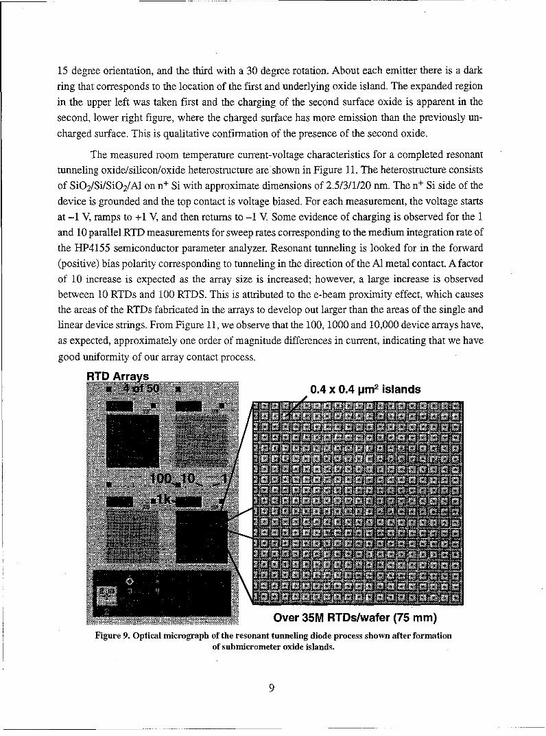
15 degree orientation, and the third with a 30 degree rotation. About each emitter there is a dark
ring that corresponds to the location of the first and underlying oxide island. The expanded region
in the upper left was taken first and the charging of the second surface oxide is apparent in the
second, lower right figure, where the charged surface has more emission than the previously un-
charged surface. This is qualitative confirmation of the presence of the second oxide.
The measured room temperature current-voltage characteristics for a completed resonanttunneling oxide/silicon/oxide heterostructure are shown in Figure 11. The heterostructure consists
of SiOjSi/SiOjAl on n+ Si with approximate dimensions of 2.5/3/1/20 nm. The n+ Si side of the
device is grounded and the top contact is voltage biased. For each measurement, the voltage starts
at -1 V, ramps to +1 V, and then returns to -1 V. Some evidence of charging is observed for the 1
and 10 parallel RTD measurements for sweep rates corresponding to the medium integration rate ofthe HP4155 semiconductor parameter analyzer. Resonant tunneling is looked for in the forward
(positive) bias polarity corresponding to tunneling in the direction of the Al metal contact. A factor
of 10 increase is expected as the array size is increased; however, a large increase is observedbetween 10 RTDs and 100 RTDS. This is attributed to the e-beam proximity effect, which causesthe areas of the RTDs fabricated in the arrays to develop out larger than the areas of the single andlinear device strings. From Figure 11, we observe that the 100, 1000 and 10,000 device arrays have,
as expected, approximately one order of magnitude differences in current, indicating that we have
good uniformity of our array contact process.
RTD Ary0.4 x 0.4 pm2 islands
,% Over 35M RTDs/wafer (75 mm)
Figure 9. Optical micrograph of the resonant tunneling diode process shown after formationof subinicrometer oxide islands.
9

Table 1. Key device parameters outlining the RTD device dimensions for the 50 different devicesincluded on the mask set in Figure 8. The submicrometer oxide island is formed in two steps. First a
pre-mesa pattern is formed to produce a large oxide mesa and clear the oxide from the greater surface ofthe wafer (75 mm). An e-beam step follows to form the submicrometer oxide island. The single-barrier
device, SB10, characterizes the second oxide barrier only.
Mesa Emitter-to-Width Mesa
Name (gim) Separation Emitter Pre-Mesa
1 EO1 0.3 x 0.3 0.1 x 0.1 0.1 2.2 x 2.2
2 E02 0.4 x 0.4 0.2 x 0.2 0.1 2.2 x 2.2
3 E03 0.5 x 0.5 0.3 x 0.3 0.1 2.2 x 2.2
4 E04 0.6 x 0.6 0.4 x 0.4 0.1 2.2 x 2.2
5 E05 0.7 x 0.7 0.5 x 0.5 0.1 2.2 x 2.2
6 E05A 0.8 x 0.8 0.5 x 0.5 0.15 2.2 x 2.2
7 E05B 0.9 x 0.9 0.5 x 0.5 0.2 2.2 x 2.2
8 E05C 1.0 x 1.0 0.5 x 0.5 0.25 2.2 x 2.2
9 El0 1.5 x 1.5 1.0 x 1.0 0.25 3.0 x 3.0
10 E1OA 2.0 x 2.0 1.0 x 1.0 0.5 3.0 x 3.0
There are four of each of the above cells that correspond to rotation angles of 0, 15, 30, and 45,and one each of the circular emitter cells below, for a total of 49 RTDs.
41 EDO0 0.3 0.1 0.1 2.2 x 2.2
42 ED02 0.4 0.2 0.1 2.2 x 2.2
43 ED03 0.5 0.3 0.1 2.2 x 2.2
44 ED04 0.6 0.4 0.1 2.2 x 2.2
45 ED05 0.7 0.5 0.1 2.2 x 2.2
46 ED05A 0.8 0.5 0.15 2.2 x 2.2
47 ED05B 0.9 0.5 0.2 2.2 x 2.2
48 ED05C 1.0 0.5 0.25 2.2 x 2.2
49 ED10 1.5 1.0 0.25 2.2 x 2.2
50 SB10 None 1.0 No mesa Single barrier
Note: Device-naming conventions: Ey means the emitter has an area of (0.y)2 square .Lm; EyRzmeans the emitter has an area (0.y)2, but the SiO2 island is rotated z degrees; EDy means theemitter diameter is O.y gtm; and SB stands for single barrier.
We can estimate the barrier thicknesses of the grown structure if we look more closely at the
positive bias polarity and compare the current densities obtained in the double-barrier and single-
barrier test structures with measurements we have obtained previously on single-barrier n+/SiO2/Al
heterostructures. Figure 12 shows a comparison of the current density measured through the 1 jim
diameter and double-barrier devices. The single-barrier devices have the first oxide layer com-
pletely removed in the area in which they appear; these devices then consist of the growth of an
undoped quantum well (4 nm) followed by ultraviolet ozone oxidation at room temperature. The
10

First Pass RTDFabrication
After EmitterBefore RIE
0.3 pm Emitter RTD
Figure 10. Scanning electron micrographs of the SiO 2/Si/SiO 2 resonant tunneling diode (wafer A4) taken afteremitter formation over the double barrier. The first oxide islands are seen as dark regions about the
submicrometer emitters.
UV-ozone oxide self-limits in thickness at about 1 nm. The oxide is then metallized with aluminumwhile still under vacuum and before removal from the growth/oxidation system.
The current density-voltage (J-V) characteristics for the single barrier can be seen in Figure
12 to correspond well with that of an oxide with thickness less than 1.6 nm, as expected. The J-V
characteristic for the double barrier corresponds to an effective oxide thickness of about 2 nm,
corresponding to a current density of about 10-2 A/cm 2. In simulation of tunneling in SiO/Si/ Si02,
we found that the resonant tunneling in these structures was not observable at room temperature
until both barrier thicknesses were near I nm, corresponding to a current density exceeding 10-1 A/
cm 2. Devices were being bonded for low-temperature measurements, but no resonance effects were
observed, even at 4.2 K.
H. Demonstration of Interconnect Process for Low Current Density RTDs
The interconnect scheme was verified on a wafer of low current density, InP-based RTDs
to demonstrate the process and to show that there are no measurement issues associated with char-
acterization of large arrays of low current density devices. Figure 13 shows the I-V characteristics
of the arrays with an order-of-magnitude increase in current for every lOX increase in array size.
The RTDs are asymmetric, showing the low voltage resonance in only one bias polarity. An elec-
tron charge storage effect (Figure 13) was found in the low current density RTDs; this is intrinsic to
the low current density Ill-V heterostructure.
11

1 04
Number of1 0 ........ RTDs in the .... ..
106 :~. Arrayl~
..... .........................S.......... . . .....
108
1 010
1 o12.
1 AG15C.TXT ' . . .1 0o141 I , . . . , . .
-1 -0.5 0 0.5 1
Voltage (V) AG15CplotI
Figure 11. Measured current-voltage characteristics for an n+ Si/SiO2/Si/SiO 2/Al resonant tunnelingheterostructure with double-barrier dimensions of 2/3/1 nm at room temperature. The array numbers
corresponding to the number of RTDs being tested in parallel (wafer A4, device ED05A, cell 4, 6; devicediameters, 0.5 pm)
I. ConclusionsWe explored two methods for forming SiO2/SiISiO 2 resonant tunneling diodes with crystal-
line silicon quantum wells. The first method, growth through voided oxide, was successful in dem-
onstrating for the first time that crystalline Si can be grown through voids in the oxide. However
conditions for forming the small void size needed to block electron transport, while allowing nucle-
ation of silicon through the oxide, were not found. A systematic search of the growth temperature-
pressure space showed that these conditions do not come naturally for the (100) and (111) surfaces.
Off-orientation could be explored, but there is no theory to guide experiments and no good reason
to believe the results will be significantly different. For this reason, we adopted a lateral-over-
growth approach in the final year to fabricate the RTD.
The SiO/Si/SiO, resonant tunneling diodes grown using the lateral silicon overgrowth pro-
cess did not show the desired negative differential resistance characteristic, but tests on these di-
odes indicate that the desired heterostructure has not yet been achieved. Further optimization of the
12

/10k, solid 1 5single barrier .0- 1'.d /1 A
S 0 • . .r .-/1 k- 21.5/..-100,.,'
1.- 2145- ,22.5101 fi ,t /lO.10• .- 24.2'S , /10k",'la,. 25.9
,-" J_1" ,&'owlbe arrier -"" ." .
@ o1 " .-0 + 28.6,,"-," -. ... ..- 29.6
S. " .- , " . " 0- • - 3 1 .2 "
1 05 -
W 10 35.1
Normalized1 gm diam.
0 0.5 1 1.5 2 2.5Voltage [ V ] AG15IJ.plotl
Figure 12. Comparison of the measured single- and double-barrier diodes against the measured characteris-tics of single-barrier Si/SiO 2/Al tunnel diodes from reference [3]. The curves from reference [2] are shown in
the range 0 to 2 V; the new measured data (for various array sizes) were taken from 0 to 0.5 V (wafer A4;device diameter, 1 Jim).
overgrowth process is needed to demonstrate the RTD. This process has now been transferred toDARPA's Si-Based Quantum MOS Technology Development program (Contract No. F49620-96-
C-0006), where it will be used for lateral overgrowth of RTD heterostructures.
Appendix F, "Beyond-the-roadmap technology: Silicon heterojunctions, optoelectronics,
and quantum devices," addresses future prospects for silicon heterojunctions and their potential for
use in device scaling and in silicon substrate, quantum well, and optical device applications.
IV. PERSONNEL SUPPORTED
Principal Investigator:
Dr. Alan Seabaugh
Distinguished Member of Technical Staff
Raytheon Systems Company
13

10-2 ...
10.4 Array__ \ Size
10 k
i- 10.8 1
0 1 0 .-1 0. .. .. .. .... .. . . .... . .....!: 0. X 0. •m2higher current trace results
0.2 X 6.2 ýrrlzfollowing negativle voltage biar V3497 and stabilizes to lower trace'E02 300 K after a single positive trace !
10-12 j . .. . . . .
-3 -2 -1 0 1 2 3VOLTAGE (V) Vs497p
Figure 13. Demonstration of RTD array contact process on HIN- resonant tunneling diodes.
Co-Principal Investigator:
Dr. Robert M. Wallace
Senior Member of Technical Staff
Texas Instruments
Dr. Yi Wei
Post-Doctoral Visiting Research Scientist
Texas Instruments
Dr. Shaoping Tang
Member of Technical Staff
Texas Instruments
Dr. Glen D. Wilk
Member of Technical Staff
Texas Instruments
Dr. Berinder Brar
Member of Technical Staff
Raytheon Systems Company
14
Dr. Paul van der Wagt
Member of Technical Staff
Raytheon Systems Company
Dr. J. Mark Anthony
Manager, Si Materials and Processing Branch
Texas Instruments
V. PUBLICATIONS
Robert M. Wallace and Shaoping Tang, "Designing materials by first-principles computational
methods," Texas Instruments Technical Journal 12 (1995), p. 66.
Yi Wei, Robert M. Wallace, and Alan Seabaugh, "Void formation on ultrathin thermal silicon oxide
films on the Si (100) surface," Applied Physics Letters 69 (1996), p. 1270.
Yi Wei, Robert M. Wallace, and Alan C. Seabaugh, "Controlled growth of Si0 2 tunnel barrier and
crystalline Si quantum wells for Si resonant tunneling diodes," Journal ofApplied Physics 81 (1997)
p. 6415.
Glen D. Wilk, Yi Wei, Hal Edwards, and Robert M. Wallace, "In situ flux cleaning technique forproducing atomically flat Si (100) surface at low temperatures," Applied Physics Letters 70 (1997)
p. 2288.
Shaoping Tang, Yi Wei, and Robert M. Wallace, "Energetics of void enlargement in thermally
grown ultrathin Si-oxide on Si (001)," accepted for publication in Surface Science Letters (1997).
Shaoping Tang, Robert M. Wallace, Alan Seabaugh, and Dominic King-Smith, "Band offset ofultrathin Si0 2.Si (001) interface: a first-principles study," to be submitted to Applied Surface Sci-
ence (1997).
VI. INTERACTIONS/TRANSITIONS
Presentations at Conferences (for the period 1 September 1994 - 31 August 1997)
Presented at the American Physical Society March Meeting, St. Louis, MO:
"Evolution of Si (100) Surface Morphology During Thermal Annealing and Post-Oxidation
Annealing," Yi Wei, Robert M. Wallace, and Alan Seabaugh
"Electronic Structure of the Ultrathin SiO2/Si(100) Interface: A First Principles Study," Shaoping
Tang, Robert M. Wallace, Dominic King-Smith, and Alan Seabaugh.
Presented at the Si-Nanoelectronics Workshop in Honolulu, HI, June 1996:
"Controlled Growth of Si-Oxide Banriers for Si-Based Resonant Tunneling Devices," Yi Wei,
15

Shaoping Tang, Robert M. Wallace, and Alan Seabaugh
Presented at the Gordon Conference on Chemical Reactions at Surfaces, Ventura, CA, March 1997:
"Energetics of Void Formation in SiO2 on Si (100)," Robert M. Wallace, Shaoping Tang, and Yi
Wei
Presented at the Materials Research Society, Boston, MA, December 1997:
"Beyond-the-Roadmap Technology: Silicon Heterojunctions, Optoelectronics, and Quantum
Devices" (Invited)
VII. NEW DISCOVERIES, INVENTIONS, OR PATENT DISCLOSURES
Filed with USPTO 18 March 1996: "Method to produce ultrathin porous silicon-oxide layer," TI-
22384.
Filed with USPTO 18 March 1996: "Method to produce ultrathin porous silicon-oxide layer em-
ploying island nucleation," TI-22978.
Filed with USPTO 14 August 1996: "Method to produce pin-hole-free, high-quality Si (100) sur-
faces using Si-flux cleaning," TI-22960.
Disclosure date 23 May 1997: "Method to grow crystalline silicon overlayers on thin amorphous
silicon dioxide layers at low temperature for the purpose of resonant tunneling diodes," TI-26176.
VIII. HONORS/AWARDS
None.
IX. REFERENCES
[1] R.W. Wallace and A.C. Seabaugh, "Silicon oxide resonant tunneling diode structure," U.S.
Patent Number 5,606,177, February 25, 1997.
[2] E. Bauer, Y Wei, T. Muller, A. Pavalovska, and I.S.T. Tsong, "Reactive crystal growth in
two dimensions: silicon nitride on Si (111)," Physical Review B51, 17891, 1995.
[3] B. Brar, G.D. Wilk, and A.C. Seabaugh, "Direct Extraction of the Electron Tunneling Ef-
fective Mass in Ultrathin SiO2 ," Appl. Phys. Lett. 69, pp. 2728-2731, 1996.
16

Appendix A
Band offset of ultrathin SiO 2.Si (001) interface: a first principles study.To be submitted to Applied Surface Science (1997).

Band offset of ultrathin SiO2/Si(100) interface: a first-principles study
Shaoping Tang 1, Robert M. Wallace 1 , Alan Seabaugh 2, and Dominic King-Smith 3
1 Materials Science Laboratory, Texas Instruments Inc., P.O.Box 655936, MS147, Dallas, Texas
752652 System Component Laboratory, Texas Instruments Inc., P.O.Box 655936, MS134, Dallas,
Texas 752653 MSI Inc., 9685 Scranton Road, San Diego, CA 92121-3752
Abstract
Using a first-principles pseudopotential approach, we have studied Si0 2/Si(100)superlattice structure constructed between f3-cristobalite Si0 2 and Si(001). Threesuperlattices containing 2, 4 and 8 layers of Si0 2 are considered. The resultsshowed that once the Si dangling bond is properly saturated, no electronic statesare present within the fundamental gap. The calculated conduction band offsetbetween Si and Si0 2 is found to increase with oxide thickness and reach asaturation value beyond the 4 layers of Si0 2 .
Introduction
The critical role of silicon dioxide and its interface with silicon for metal-oxide-semiconductor(MOS) technology can never be overemphasized. The physical and electronic propertiesassociated with the Si0 2 /Si interface determines the fundamental device operational parameters.As MOS critical dimensions continue to scale down, there is an increasing need to fullyunderstand the physical and electronic structures of the Si0 2/Si interface.
Unfortunately, much remains to be understood about the detailed interface atomic and electronicstructure, despite a great deal of efforts to grow thin-oxide layers on Si surface in the last threedecades. Previous studies generally supported an interface model with a non-stoichiometrictransition region separating crystalline Si and amorphous Si0 2 . However, a flurry of recentexperiments showed evidence that an abrupt and ordered interface structure between Si and Si0 2
is formed. Theoretical simulations of such interface had been hampered partly by the uncertaintyand complexity of the interface structure.
The core-level spectroscopy measurement on Si0 2 /Si interface showed that there are suboxidespecies at the interface[l]. TEM and X-ray reflectivity studies showed the evidence of orderedstructure in the Si/Si0 2 interface[2,3]. A recent theoretical calculation by Pasquarello, Hybertsonand Car [4] on a model Si0 2/Si interface derived from tridymite Si0 2 grown on Si(100)provides a detailed analysis of bond length and bond angle distributions at the interface. Theirresults also suggested that a transition region which is similar to amorphous bulk Si0 2 exists atthe SiO 2/Si interface. These studies contribute substantially to the understanding of the atomicand electronic structure of Si0 2 /Si, although none of the proposed structures has beenunambiguously accepted.

in this work, we aim at gaining a basic understanding of the electronic properties of SiO2/Siinterface using a structural model proposed by Herman, Batra and Kasowski[5] (thereafterreferred as HBK model). We studied three superlattice structures containing alternate Si andSiO 2 layers as a function of varying the thickness of the included SiO2 layers. Because of theway the model is constructed, a Si dangling bond exists at the interface within a unit cell.Himpsel et al. [1] suggested using H, 0 or OH to saturate the Si dangling bond. Our studyshowed that a single hydrogen atom is unable to perform the complete saturation of a danglingbond in the HBK model. On the other hand, a single oxygen can form a double bond with a Siand completely saturates the Si dangling bond. This 0 saturation leaves no interface states in thefundamental gap of the superlattice.
Methodology and models
We used a first-principles plane wave pseudopotential method[6] based on the local densityapproximation (LDA) to density functional theory. The exchange-correlation energy iscalculated using a parameterized form of the exchange-correlation energy[7] of thehomogeneous electron gas obtained using quantum Monte Carlo techniques[8]. Norm-conserving pseudopotentials constructed within the scheme developed by Troullier andMartin[9] are used. The wave functions are expanded in a plane-wave basis set with an energycutoff of up to 30 hartrees. One special k point is used for sampling k space[ 10].
Figure 1: The construction of HKB Si0 2/Si interface model.
The Si/SiO2 interface is constructed according to the HKB model[5] assuming that a f3-cristobalite SiO 2 is epitaxially grown on Si(0O 1) surface, shown in Figure 1. By rotating the unitcell of P-cristobalite by 450, one can get a smaller tetragonal unit cell which can align withSi(001) substrate provided that the lattice constants of this tetragonal cell is the same with Si. Inpractice, we expand the Si0 2 lattice constant by 6.8% to allow an epitaxial growth of Si0 2 onSi(0O 1). The virtue of this model is its relative simplicity and the ease of incorporating variouschemical imperfections at or near the interface. Additionally, the strain imposed on the SiO 2structure, relative to the Si lattice (6.8% lattice mismatch), is smaller than other known phases ofSi0 2 . Previous experimental studies also suggest that this structure may be close to the realinterface structure. Figure 2 shows the three structural models we used in the calculation. Eachmodel has four Si layer sandwiched between Si0 2 . The smallest structure is (Si)4(SiO 2 )2 whichcontains 2 Si0 2 layers of thickness of 3.8A and the largest structure is (Si) 4 (SiO 2 )8 that containseight layers of Si0 2 with a thickness of 15.4A. An alternative interface model based on the

tridymite SiO 2-Si interface has been studied theoretically by Pasquarello, Hybertsen and Car[4].However, the mismatch between tridymite Si0 2 and Si is much larger than that from cristobalite(-12%).
Si/Si0 2 interface structural models
(SW4(St02a i (Si)4(SiO 2 )A (Sp ic(St0 re A
(a) (b) (C)Figure 2: Three SiO2/Si interface models used in the calculation.
Results and discussion
Band structures
We start with a (Si)4(SiO2)2 superlattice structure shown in Figure 2(a). At the Si-SiO2
interface, there are two Si dangling bonds pointing to the oxide. Initially, these dangling bondswere saturated by oxygen. Without considering the lattice relaxation, the calculation showed that,there is an indirect fundamental gap of 0.56eV. The actual bandgap, of course, should be largerthan 0.56eV as it is well known that LDA theory always underestimates excited state propertiessuch as the band gap. If the atomic positions are fully relaxed, the bandgap is still indirect, butthe calculated gap size is increased to 0.7eV. This result shows that an unrelaxed (i.e. strained)interface structure has smaller bandgap than the relaxed structure.
We also performed the calculation on (Si) 4 (SiO 2 )2 structure by using H to saturate the Sidangling bonds at the interface. The purpose of such study is to simulate the effect of a Himpurity on the electronic band structure, since hydrogen incorporation is unavoidable in thematerials processing. We find that H does affect the band structure by introducing two interfacestates within the forbidden band. These states fill the bandgap and make this Si-SiO 2 superlatticemodel exhibit metallic electronic behavior.
In another attempt to simulate the various interface conditions, we studied the structure(Si)4 (SiO 2 )2 assuming that Si dangling bonds are not saturated at the interface. The results showthat two unoccupied surface states appear in the forbidden band. These surface states can readilyinteract with any impurities at the interface and introduce unwanted electronic states.
In order to evaluate the effects of thickness variation of the Si0 2 layer on the overall bandstructure, we studied a four layer Si0 2 superlattice structure (ie. (Si) 4 (SiO 2 )4) shown in Figure2(b)) while the Si layer is kept the same as the previous two layer Si0 2 HKB structure. Thecalculation is done without considering the lattice relaxation. The results show that this four

tructure has an indirect bandgap of 0.91eV which is 0.35eV larger than that of
)2 HKB structure. This result, coupled with the fact that bulk SiO 2 has asuggests that the bandgap of SiO 2-Si superlattice increases with the thickness
tlation
, most important parameters characterizing heterojunctions are the valence anddiscontinuities (or band offset). The knowledge of these quantities is essentialae transport properties of the interface, or the electrostatic potential in avice. A main problem in calculating the band discontinuity is to correctly lineie two materials at the interface. This information can not be obtained from the
alone because no absolute energy reference is defined in a infinite solid
-come the band line up problem was developed by Van de Walle and Martinto calculate the average potential for each bulk material and then calculate theom one material to another at the interface from a combined heterojunctiona superlattice structure. The potential shift between the two materials is used to)etween the average potential of each bulk material. Figure 3 illustrates this ideaterface as an example. The average potential of each bulk material (i.e. Si and-d by a potential AV which is calculated from the Si/SiO 2 superlattice. Theduction band offset can then be obtained based on the band gap value and the;ition (Ev) relative to the average potential for each material.
•IE.
AEý
E,=8.9ev
AE,
*.. .. .. Vsio 2AV
Si0 2
natic representation of band lineups. The calculated potential shift (AV) acrosstermines the lineup of average potential in the bulk.
potential shift and the corresponding valence (AEv) and conduction (AEc) bandinterface models are listed in Table 1. It can be seen that the conduction band
*along with the increase of the oxide thickness. It has to be emphasized that these| for determining trends and not for quantitative description (values) of the band
for the (Si)4 (SiO 2)2 model where only two layers of SiO 2 is included, theI offsets have potentially large error because the band gap of this thin SiO 2 layeris reasonable to assume that the bandgap of this thin oxide region is smaller than
d gap (8.9eV). Thus, the conduction band offset result for this model (1.71eV) isactual value. Another error in such calculations comes form the models assumed

because these were constructed using a expanded SiO2 lattice (with 6.8% expansion) stacked onSi(001) (Figure 1). The uncertainty of the band gap of the expanded SiO 2 will also introducesome error in the calculation. Our calculations showed that the expanded SiO2 lattice will havesmaller band gap than the regular SiO 2 lattice. As a result, the band offset result in Table 1 willbecomes smaller.
Table 1: The potential shift (AV) across the Si/SiO 2 interface and the valence and conductionband offset for three different structural models.
interface (Si) 4 (SiO 2) (Si) 4(SiO 2 ) (Si)4(SiO 2 )
2 4 8AV (eV) 0.65 5.85 5.85AEv (eV) 6.02 0.82 0.82AEc (eV) 1.71 6.91 6.91
To estimate the effect of an expanded SiO 2 lattice on the band offset calculation, we studied thebandgap of a regular SiO 2 bulk and an expanded SiO 2 bulk with a 6.8% expansion of regularlattice constant of a SiO2 . The calculated band gaps are 5.46eV and 4.70eV respectively. Thus,it is not surprising to see that the calculated band gap (5.46eV) of SiO 2 is smaller than theexperimental result (8.9eV), because of the well known underestimation of band gap by LDAmethod. To adjust the calculated band gap to experimental result, a factor of 1.63 is used to bringthe theoretical band gap result in line with the experimental result. Using the same factor, we canobtain the estimated band gap of the 6.8% expanded SiO2 lattice to be 7.66eV. If this band gapresult is used, the conduction band offsets are shown in Table 2. Compared to Table 1, it can beseen that all conduction band offsets are shifted down.
Table 2: Revised valence and conduction band offset for three different structural models atSi/SiO 2 interface.
interface (Si) 4 (SiO 2) (Si) 4(SiO 2 ) (Si)4(SiO 2 )2 4 8
AEv (eV) 6.02 0.82 0.82AEc (eV) 0.47 5.26 5.26
An important result from the present study is that the band offset reaches a saturation value afterfour layers of Si-oxide which is about 7.5A. This shows that the thin Si-oxide film will thereforehave bulk-like electronic properties after this thickness. Atomic relaxation studies on(Si) 4 (SiO 2 )2 and (Si) 4(SiO 2 )4 models showed a large atomic relaxation within the 7.5A region.
In summary, we have studied the electronic structure of Si-SiO2 interface using a first-principlepseudopotential method. The results showed that no electronic states are present within thefundamental gap. An important conclusion is that the conduction band offset increases with thethickness of the oxide and reaches a constant value beyond 7A oxide thickness. Our study alsoshown that a relaxed superlattice structure yield larger bandgap than a strained superlattice.
References:[1] F.J. Himpsel, F.R. McFeely, A. Taleb-Ibrahimi, J.A. Yarmoff, and G. Hollinger, Phys. Rev.B 38, 6084(1988).

[2] T.A. Rabedeau, I.M. Tidswell, P.S. Pershan, J. Bevk, and B.S. Freer, Appl. Phys. Lett, 59,3422(1991).[3] A. Ourmazd, D.W. Taylor, J.A. Rentschler, and J. Bevk, Phys. Rev. Lett., 59, 213(1987).[4] A. Pasquarello, M.S. Hybertsen, and R. Car, Appl. Phys. Lett. 68, 625(1996); ibid, in 2ndInternational Conference on Physics of Semiconductor, ed. D.J. Lockwood, vol. 1, 1994, p. 6 12 .[5] F. Herman, I.P. Batra and R.V. Kasowski, "Electronic Structure of a Model Si-SiO 2
Interface", in the Physics of SiO2 , ed. by S.T. Pantelides, Pergamon Press, 1978. p.3 3 3 .[6] PlaneWave code is a software package from Molecular Simulation Incorporated.[7] M.P. Teter, unpublished(1990). This parameterization of the exchange correlation energy isvery similar to the one proposed by Vosko et al. in S.J. Vosko, L. Wilk and M. Nusair, Can. J.Phys., 58, 1200(1980).[8] D.M. Ceperley and B.J. Alder, Phys. Rev. Lett., 45, 566(1980).[9] N. Troullier and J.L. Martins, Teter, Solid State Communications, 74, 613(1990).[10 ]H.J. Monkhorst and J.D. Pack, Phys. Rev. B 13, 5188(1976).[11] C. G. Van de Walle and R.M. Martin, Phys. Rev. B 35, 8154(1987).

Appendix B
In situ flux cleaning technique for producing atomically flat Si (100)surface at low temperatures, Applied Physics Letters 70 (1997) 2288.

In situ Si flux cleaning technique for producing atomically flat Si(100)surfaces at low temperature
G. D. Wilk,a) Yi Wei, Hal Edwards, and R. M. WallaceCentral Research Laboratories, Texas Instruments, Dallas, Texas 75265
(Received 4 November 1996; accepted for publication 28 February 1997)
We have developed a method for removing oxides and producing atomically flat Si(100) surfaceswith single atomic height steps using a Si flux cleaning technique. By introducing a Si flux in therange 1.0-1.5 A/s at the onset of an SiO 2 thermal desorption step as low as 780 'C, scanningtunneling microscopy (STM) and atomic force microscopy images reveal smooth surfaces withatomically flat terraces with an rms roughness of 0.5 A and single-step heights of 1.4 A. STMreveals that A- and B-type steps are present across the entire area of the scanned surface. Desorptionof the surface oxide layer with Si fluxes below this range results in rougher surfaces with pits -50A deep and 1000 A across. For Si fluxes above this range, no pits are seen but atomic steps are notvisible on the surface. © 1997 American Institute of Physics. [S0003-6951 (97)04017-5]
Device scaling in CMOS is requiring ever thinner gate mation of a chemical oxide as a protective cap on the Sioxides while still demanding high reliability of these oxides. surface. Once the sample is placed in vacuum, resistive orThe gate oxide thinning trend is now placing more focus on radiative heating is used to anneal the sample at 800-900 'Cthe interface between the Si0 2 layer and the Si substrate as a for several minutes to desorb the oxide. Various low Si depo-means of identifying the sources of premature breakdown sition rates (-0.1-0.6 A/s) have also been used14-16 for sev-and perhaps improving reliability.1- 3 The interface rough- eral minutes in an attempt to improve the surface quality forness depends strongly on the cleaning procedure used in pre- subsequent thin-film growth. While the emergence of reflec-paring the Si surfaces, and standard techniques4' 5 of produc- tion high-energy electron diffraction (RHEED) streaks anding a surface oxide cap followed by an in situ anneal step at spot patterns was used as an indication of oxide removal in800-900 TC can actually produce pits on the surface which some of these studies, it was assumed that these processesare 50 A deep and up to 1000 A across. For thin-film growth, yield a flat, uniform surface. Under many oxide desorptionthis large roughness can significantly affect the properties of conditions, however, a rough surface can result which maythe film. have a significantly detrimental effect on ultrathin film prop-
It has been suggested for thick oxides6 8 (-200 A) and erties, particularly where a uniform interface is required. Tofor thin oxides 9-12 (_-30 A) that the pits form by SiO etching our knowledge no one has investigated the Si surfaces withof the substrate, where suboxides (SiOx ,0<x<2) near the atomic resolution probes following these treatments. An ininterface desorb as volatile SiO molecules, followed by re- situ Si surface cleaning technique which uses relatively lowduction of the oxide layer in the reaction Si0 2+Si temperatures and yields an atomically flat, stepped surface is-2SiO (g). Mobile Si monomers are suggested'° to form in very desirable. In this letter, we describe a Si flux cleaningthe substrate voids left by the suboxides near the interface technique which can be used to obtain atomically flat, single-which then reduce SiO 2 molecules to the volatile SiO form, height steps on Si(100) at temperatures between 700 andwhich desorbs from the substrate. Engel et al.9 has also ar- 800 'C. The surface cleaning conditions have been varied asgued through energetics considerations that the formation of a function of Si deposition rate and substrate temperature.mobile monomers is the rate-limiting step in the reaction. The substrates were nominally flat 4-in Si(100), n-typeRecent investigations on the void growth process, however, wafers with p=0.01-0.02 f cm. Some of the as-receivedsuggest that mobile Si monomer formation and SiO forma- wafers were placed directly into a molecular beam epitaxytion are kinetically competing processes on the Si surface.' 3 (MBE) chamber without any ex situ chemical cleaning, while
While this method removes the oxide, it does so at the ex- others received an initial degreasing with acetone and metha-pense of forming pits in the Si substrate. It is very desirable, nol. The substrates where heated radiatively by a strip heaterhowever, to remove the oxide without forming pits in the near the backside of the wafer. A thermocouple placed nearsubstrate and also without using chemical etching. Removing the substrate was used for temperature measurements. Sincethe chemical etching steps could reduce and simplify the the substrate holder rotates during the surface preparationnumber of surface preparation steps used in standard pro- procedure, direct contact between the thermocouple and sub-cessing procedures. Further, while HF etching removes the strate was not possible. The thermocouple was calibrated tooxides and yields a smooth, H-terminated surface (rms an optical pyrometer over the temperature range used in thisroughness -1 A), there is no well-ordered structure to the experiment. While the temperature reproducibility wassurface. An atomically flat Si surface with well-ordered steps +5 'C, the absolute temperature is accurate to ±25 °C. Aftercan be obtained by flashing the sample at 1200 'C but this a long degas at 400 'C, the wafers were heated up to 650 'C,process is not practical for large wafers and thermal budget at which point the wafer surface was exposed to the Si flux.concerns. The anneals were then done at various temperatures and
A typical surface preparation method starts with the for- times while the Si flux impinged on the substrate. The base
pressure in the MBE chamber was 5 X 10- 11 Torr, and wasa)Electronic mail: [email protected] - 8 X 10⁻¹⁰ Torr during Si deposition. Following the Si flux
2288 Appl. Phys. Lett. 70 (17), 28 April 1997 0003-6951/97/70(17)/2288/3/$1l.O0 © 1997 American Institute of Physics

P % , , ...
*114
S' . '* 444P 9I
44
FIG. 1. IO10× um /2 AFM image of Si(100) with a native oxide which hasbeen partially desorbed by annealing at 780 'C for 30 min. A high density ofvoids (1000-5000 A wide, 40 ,A deep) is seen on the surface.
cleaning step, the wafers were removed from vacuum,cleaved and transferred in air as rapidly as possible (nolonger than 30 min) for STM (in UHV after transfer) andatomic force microscopy (AFM) (in ambient, performed in r:,,•"tapping" mode) analyses,., ..
Figure I shows a 10× 10 /=m2 abetAMiaeo
Si(100) surface which has undergone a partial thermal de- ,< •......sorption of the native oxide. The sample was heated at ••780 'C for 30 min under UHV conditions. A very high den-sity of holes is clearly seen across the surface. The holesrange from -500 to 5000 A& wide and are -40 ,A deep. The FIG. 2. (a) 10X 10 /.Lm2 AFM image of Si(100) after complete desorption
initial native oxide is still present in the regions between the of the native oxide. The sample was annealed at 780 'C for 30 rain with a Sihols.Wih o S fuxprvied urngth anea sep i i deposition rate=0.3 ,Z/s being introduced for thefina1 10 rain of the anneal.
7 ~ (b) 0.5 X 0.5 /.Lm2 STM image of the sample in Fig. 2(a). The holes reflectseen that a rough, nonuniform surface results,.h orfl ymtyo h usraeadata tppnigcnes
Figure 2(a :) shows a 10 X 10 Azm2 AFM image of a tefu-odsmer ftesbtaeadata tppnigcnes
Si(100) surface (initially containing a native oxide) whichhas been annealed at 780 'C for 30 min, with a Si flux (-0.3 Azm2 in AFM). The measured rms roughness is 0.5 .A for thisA/s of Si) being introduced for the final 10 min of the anneal image. Alternating A-type (smooth) and B-type (rough) stepsonly. While etching of the substrate still occurs, the void can be seen in the image which indicates a smooth, highdensity and size have been reduced by the addition of a Si quality surface with 1.4 A• single atomic height steps. Thisflux during, the anneal. Figure 2(b) shows a 5000 image reveals an extremely well-defined step structure on the× 5000 ,k2 UHV STM image of the sample in Fig. 2(a). surface. Atomically flat surfaces such as this one were oh-Compared to the surface in Fig. 1, the surface is much served for all samples which were Si flux-cleaned with the Sismoother between the voids, and the voids themselves are deposition rate between 1.0 and 1.5 A•/s.much better defined: there is clearly a four-fold symmetry to Most Si cleaning, methods which use Si deposition tothe voids, reflecting the symmetry of the Si(100) substrate. improve the surface quality introduce a Si flux at some pointThe addition of a Si flux has resulted in a clean surface and after the heating has been initiated, and often it is done afterthe formation of a well-defined step structure corresponding the anneal step has been completed. This work demonstrates,to the original miscut angle of the surface. This indicates that however, that it is critical that the Si flux be started at thealthough the addition of a Si flux for the final 10 min helps to onset of the heating step, in our case 650 'C, so that reduc-reduce the void size and density, it does not prevent void tion of the oxide at the top surface prevents oxide reductionformation. The holes also appear to act as step pinning cen- at the interface. It is also essential that Si is deposited at anters, as the image shows several steps with very small terrace appropriate rate to compete with the interfacial reduction re-widths near the hole edge. This behavior may contribute to action. For Si deposition conditions outside of the range ofthe depth of the holes in addition to substrate etching by SiO 0.2-22k/s, the surface becomes significantly rougher. For Siformation. deposition rates below -0.2 ks, Si is not supplied quickly
Figure 3 shows a 1 X I jtm 2 STM image of a Si(100) enough to reduce SiO2 from the top surface, and voids formsurface (initially containing a native oxide) which has been from reaction at the bottom SiO2 interface. For depositionannealed at 780 'C for 10 min, with the Si flux (-I k•sý rates higher than -2 ,k/s, Si deposits too quickly for the
being introduced at the onset of the thermal anneal (at decomposition to occur, thus excess Si blankets the surface650 'C, followed by a temperature ramp up to 780 °'). No and creates less well-defined steps. It is also possible that notholes are visible (larger-area scans show no holes across 100 all of the SiO2 is desorbed in this case, which would account
Appl. Phys. Lett., Vol. 70, No. 17, 28 April 1997 Wilk eta!. 2289

FIG. 3. 1 X I gzm2 STM image of Si(100) after desorption of the native FIG. 4. 1 X 1 /.m
2 STM image of a Si sample initially containing a nativeoxide at 780 'C for 10 min with a Si flux of -1 A,/s, introduced at the onset oxide after an anneal at 800 'C for 10 min with a Si flux of 6 A/min. Aof the thermal desorption step. The measured rms roughness is 0.5 A and highly nonuniform surface results with a high density of large holes. Theboth A-type and B-type single atomic height steps can be seen. inset shows the corresponding RHEED pattern taken from this surface.
for the less well-defined surface structure. The optimum Si than that at the interface. Since the Si atoms arrive uniformly
deposition rates were found to be 1.0-1.5 ks, where STM as monomers in the flux, the activation barrier for Si mono-and AFM both observed atomically flat terraces and single- mer formation is removed. Recent calculations suggest' 8 thatheight A- and B-type steps (as seen in Fig. 3). Within this the activation energy for Si monomer formation from therange, it appears that the Si monomer arrival rate is balanced 2X 1 reconstructed surface is comparable to that for reduc-with the SiO2 reduction rate and a high-quality surface can tion of SiO2 to SiO. If this is the case, the reaction at thebe obtained, oxide surface may occur more rapidly than the interface re-
These results indicate that at low deposition rates a action. For very thin oxides (-_30 A), the SiO2 layer can berough, very nonuniform surface results. We reproduced pre- completely removed before voids of significant size form atviously reported cleaning conditions by preparing a sample the interface. For thicker oxides (>30 A), significant reduc-with an anneal step at 800 'C for 10 min and a Si flux of -6 tion of the oxide may be unavoidable by this technique, butA/min, which closely approximates the rate of -8 A/min at the Si flux cleaning method should work well for oxides800 °C as suggested by others.' 5 Figure 4 shows a 1 formed in air and by standard chemical cleaning procedures.XI 1um2 STM image of the surface under these conditions. The authors thank Marshall Howell and John Powell forIt can be seen that the surface is marked by a very high their excellent technical assistance and J. P. A. van der Wagtdensity of pits which are -50 A deep. The inset of Fig. 4 for very useful discussions.
shows the corresponding RHEED pattern from this surface,which contains streaks normally associated with a smooth,reconstructed crystalline surface. Although RHEED is often 'K. F. Schuegraf and C. Hu, Semicond. Sci. Technol. 9. 989 (1994).
2C. j. Sofield and A. M. Stoneham, Semicond. Sci. Technol. , 215 (1995).used as an indicator for smooth, uniform and crystalline sur- 3 H. S. Momose, M. Ono, T. Yoshitomi, T. Ohguro, S.-I. Nakamura, M.
faces, defects of this type will yield a deceptive RHEED Saito, and H. Iwai, IEEE Trans. Electron Devices 43, 1233 (1996).
pattern which may be mistaken for a high-quality surface. 4 Ishizaka, N. Nakagawa, and Y. Shiraki, Proceedings of the 2nd Interna-The presence of pits is expected only to decrease the inten- tional Symposium on Molecular Beam Epitaxy (Japanese Society of Phys-
h7 Iics, Tokyo, Japan, 1982), p. 182.sity of and slightly broaden the RHEED spots.7 It is clear 5 W. Kern, Handbook of Semiconductor Wafer Cleaning Technologythat this type of RHEED pattern may be incorrectly inter- (Noyes, Park Ridge, NJ, 1993).
preted without STM examination of the surface. These sur- 6 R. Tromp, G. W. Rubloff. P. Balk, F. K. LeGoues, and J. van Loenen,
face nonuniformities can have a profound effect on any sub- Phys. Rev. Lett. 55, 2332 (1985).tfilm growth. 7 M. Liehr, J. E. Lewis, and G. W. Rubloff, J. Vac. Sci. Technol. A 5, 1559
sequent f(1987).At substrate temperatures up to 900 'C, the surface 8G. W. Rubloff, J. Vac. Sci. Technol. A 8, 1857 (1990).
maintains sharp single-height steps and atomically flat ter- 9 Y.-K. Sun. D. J. Bonser, and T. Engel, Phys. Rev. B 43, 14309 (1991).
races. This behavior is not surprising, as an increased Si 10 Y.-K. Sun, D. J. Bonser, and T. Engel, J. Vac. Sci. Technol. A 10, 2314adatom diffusion lenth maintains hih surface quality. At 1992).a o d o l11 K. E. Johnson and T. Engel, Phys. Rev. Lett. 69, 339 (1992).much higher temperatures, however, it is expected that sur- '2K. E. Johnson, P. K. Wu, M. Sander, and T. Engel, Surf. Sci. 290, 213
face roughening will occur during deposition. High-quality (1993).surfaces have also been observed down to temperatures of '5 Y. Wei. R. M. Wallace, and A. C. Seabaugh, Appl. Phys. Lett. 69, 1270(1996).700 °C, although the step edges are not as well defined and 'M. Tabe, K. Arai, and H. Nakamura, Jpn. J. Appl. Phys. 20, 703 (1981).the terraces show more roughness. Within large windows of 15 M. Tabe, Jpn. J. Appl. Phys. 1 21, 534 (1982).
deposition rate and substrate temperature, very high-quality 16K. Kugimiya, Y. Hirofuji, and N. Matsuo, Jpn. J. Appl. Phys. 1 24, 564
Si surfaces can be obtained using this technique. e(1985).Z>ni 17J. E. Mahan, K. M. Geib, G. Y. Robinson, and R. G. Long, J. Vac. Sci.
This method appears to work well because the oxide Technol. A 8, 3692 (1990).
reduction reaction at the surface has one less reaction step 18S. Tang (private communication).
2290 Appl. Phys. Lett., Vol. 70, No. 17, 28 April 1997 Wilk et al.

Appendix C
Void formation on ultrathin thermal silicon oxide films on the Si (100)surface, Applied Physics Letters 69 (1996) 1270.

Void formation on ultrathin thermal silicon oxide filmson the Si(100) surface
Yi Wei, Robert M. Wallace, and Alan C. SeabaughTexas instruments Incorporated. Dallas, Texas 7.5265
(Received 8 March 1996; accepted for publication 1 July 1996)
The formation of voids on the thermally grown (650 °C) ultrathin (-I nm) silicon oxide films onthe Si(100) surface was investigated by using ultrahigh vacuum scanning tunneling microscopy.Voids form randomly on the ultrathin oxide film upon thermal annealing at 750 'C. In contrast tovoid formation observed on thicker (>5 nm) thermal silicon oxide films and that observed onultrathin (-1 nm) oxide films formed by room temperature 02 adsorption, the number of voidsincreases during annealing. We find that Si monomer creation and SiO production competekinetically in the void formation process. © 1996 American Institute o' Physics.[S0003-6951(96)02735-0]
The ultrathin silicon oxide film and its interface with with Si-monomer formation as a rate limiting step in voidsilicon have drawn increased attention in recent years due to development.the continued scaling of metal-oxide-semiconductor (MOS) The experiments were performed in a multiple-chamberdevice technology. Transistors with ultrathin gate oxides ultrahigh vacuum (UHV) system equipped with a scanningwell within the direct tunneling regime (_-3 nm) have been tunneling/atomic force microscope" and a monochromaticrecently demonstrated.' Moreover. prospects for Si-based na- x-ray photoelectron spectroscopy (XPS) system.' 2 Thenoelectronic devices, such as resonant tunneling diodes, de- samples were P-doped n-type Si(100) (p=0.l & cm). Thepend critically on the control of ultrathin, Si-compatible tun- surfaces were cleaned by standard resistive heating methodsnel barrier materials. 2 The thermal stability of ultrathin oxide resulting in well-ordered Si(100)-(2x 1) reconstruction withfilms is a prerequisite to the production of either of these very low defect density (<2%). Surface temperature wasdevices. monitored by calibrated optical pyrometry. Chemical analy-
Void formation on thermally grown oxide films.' 5 ul- sis of the surface by XPS indicated that impurities were be-trathin oxide films formed by room temperature 02 low the detectable limits (<1%). The ultrathin (-I nm) ox-adsorption,6-8 and native oxide films9 has been studied pre- ide films were formed thermally by exposure to 5 X 10⁻⁵viously. At elevated temperatures and subatmospheric pres- Torr 02 at 650 'C for 90 s. The thickness of the oxide filmsures, silicon oxide films decompose by the interfacial reac- was determined by XPS.13,' 4 The morphological evolution oftions Si+SiO2-+2SiO(g)."' The decomposition of the oxide the voids after thermal annealing in UHV was measured byfilm is spatially inhomogeneous: decomposition starts locally STM.and proceeds laterally as the reaction proceeds at the void After the oxide was grown, no long-range atomic struc-perimeter. The clean surface of the void is lower than the ture can be resolved by STM. In contrast to the case of RToxide/Si interface due to bulk Si consumption.5 7 This 02 adsorption, 7,8 steps and terraces which correspond to themechanism leaves the oxide areas between the voids unper- underlying Si(100) substrate are not observed.turbed, i.e., there is no oxide film thinning observed. For Figure 1 is a series of STM images showing the se-thermal oxide films of 50-500 A thick,3 4 it has been sug- quence of void formation when the ultrathin thermal oxide isgested that the voids are nucleated at defect sites. The void annealed at 750 'C for different durations. Before the voidssize grows linearly with time for diameters in the range 2-80 start to overlap [Fig. 1(a)], the sizes of the voids observedýtm, but the number of voids is nearly unchanged with con- here (-300-400 nm 2 ) are much smaller than those ob-tinued annealing at T> 1000 °C. This behavior was attrib- served on thicker thermal oxide films (_-3 Azm 2)3.4 bututed to the perimeter interfacial SiO reaction as the rate lim- larger than those observed on ultrathin oxides grown by theiting step in void development. means of RT 02 adsorption (-_40 nm2) 6-8 at comparable
In previous scanning tunneling microscopy (STM) stud- annealing temperatures. The depth of the voids in the regionies of oxide films formed by room temperature (RT) 02 depicted in Fig. 1(a) is estimated to be 1.2 nm by STM andadsorption, 7.8 much smaller voids were observed on anneal- is uncertain due to the differences in the tip-Si and tip-ing and again no new voids were observed once desorption oxide tunneling barriers.was initiated. However, modeling of the void size evolution It is apparent from the STM image sequence that thewith annealing indicated that the production of a mobile Si void density increases with annealing duration. Also, beforemonomer is the rate limiting step in void development. the void density increases to the point that the voids start to
In this letter, we present the results of void formation on coalesce [Fig. 1(c)], the void size initially increases and ap-ultrathin thermal oxide films (- ] nm thick). A mechanism pears to reach a limiting size. From such STM images takenfor void formation is observed where the number of voids before the voids started to strongly overlap (i.e., individual(void density) increases with annealing and existing voids voids can still be distinguished), we measured the void den-continue to grow marginally. These results are consistent sity [Fig. 2 (0)] and averaged void size [Fig. 2 (0] as func-
1270 Appl. Phys. Lett. 69 (9), 26 August 1996 0003-6951/96/69(9)/1270/3/$10.00 © 1996 American Institute of Physics

30 - 1 1 1 1 1 1 '6
25-
C4
E 20-N e/ 0
0. _ 15 o 4
10 - I>0
.25-
0-
0 1 2 3 4
Annealing Time (min.)
FIG. 2. Void number density (0) increases linearly with annealing duration.A marginal increase in void size (0) is observed with annealing.
voids results from SiO formation at the interface which mustdiffuse through the oxide film to escape from the interface.Assuming that defect sites in the thicker oxide films or at theoxide/Si interface provide efficient pathways for SiO libera-tion, the voids would prefer to open about these oxide defectsites. The spatial resolution limitations of the electron mi-croscopy methods employed in the earlier studies3-5 and theSiO diffusion processes are likely the cause for the failure ofthe detection of the voids of the size reported here, althoughthe existence of "microvoids" (smaller than thosereported here) was supported from positron-annihilationexperiments.4
In ultrathin Si-oxide films, the SiO formed at the inter-face is readily liberated and does not require oxide defectpathways. Thus it is reasonable that void formation wouldproceed randomly throughout the oxide film and the void
FIG. 1. Evolution of oxide void formation after annealing at 750 'C for (a) density would continue to increase, as is observed here. In30, (b), 90, and (c) 120 s durations. Scan area of all images is 500 nmX500 previous studies of void formation on ultrathin oxidesnm; sample bias +3 V. formed by room temperature 02 adsorption,7,8 it was con-
cluded that the production of a mobile monomer (which thentions ofannealing duration to reveal this dependence. These diffused to the void perimeter to react with oxide to formresults are in contrast to the void formation observations on SiO) is the only rate limiting step. The diffusion of Si mono-thicker thermal oxide films where void density was constant mer on ideal Si(100) surfaces has been examinedand the void size increased linearly with annealing duration experimentally' 5 and in theoretical treatments! 6- 18 where ac-at T> 1000 'C. A similar observation of constant void den- tivation energies of diffusion < 1 eV have been reported.sity was also reported for the RT ultrathin oxides.7 "8 We Although the void base surface morphology here is consid-observe an increase in void density in the ultrathin thermal erably more complicated than the ideal Si(100) surfacesoxide during annealing; our results suggest that the density studied, we also assume that the monomer diffusion to theof defects which gives rise to void formation in ultrathin perimeter is facile.Si-oxide films also increases with temperature. We also ob- The increase in void density with annealing duration ob-serve a decrease in the rate of void growth (area) which served concomitantly with marginal void growth under thesuggests that the rate of void growth is affected by the UHV conditions employed here is alsoconsistent with the forma-annealing process while the rate of void nucleation is not. tion of a Si monomer as the rate limiting step in void
The difference in void formation behavior between thick development. 7.8 Experimental evidence for the activation en-
and ultrathin Si-oxide films is intriguing. Under the growth ergy for mobile Si-monomer formation is lacking, but esti-conditions here, the SiO formation reaction occurs at the mates of -3.5-4 eV are consistent with Si adatom bondoxide/Si interface. For thicker oxide films, initiation of the scission (3 eV) and bulk Si bond scission (4.3 eV). 17"18 Re-
Appl. Phys. Lett., Vol. 69, No. 9, 26 August 1996 Wei, Wallace, and Seabaugh 1271

cently, we calculated the activation energy of Si-monomer 1M. Ono, M. Saito, T. Yoshitomi, C. Fiegna. T. Ohguro. H. S. Momose.
formation to be in the range of 3.2-4 eV using first- and H. Iwai. J. Vac. Sci. Technol. B 13, 1740 (1995).principles density functional theory. 9 As experimental re- 2A. C. Seabaugh. C.-C. Cho. R. M. Steinhoff, T. S. Moise. K. H. Park. and
Y. Okuno. Silicon-Based Resonant Tunneling (R & D Association forsuits indicate that the activation energy for SiO formation is Future Electron Devices. Tokyo, 1996), Vol. 6.
3.2-3.6 eV,6 "8 the observed marginal increase in void forma- 3 M. Liehr. J. E. Lewis. and G. W. Rubloff, J. Vac. Sci. Technol. A 5, 1559
tion here is consistent with this estimate. Thus, at the tem- (1987).
perature employed here (750 'Q, the creation of the Si o4G. W. Rubloff. J. Vac. Sci. Technol. A 8. 1857 (1990).5 R. Tromp, G. W. Rubloff. P. Balk, F. K. LeGoues. and J. Van Loenen.
monomer and the SiO production competes kinetically in the Phys. Rev. Lett. 55, 2332 (1985).
void formation process. 6Y.-K. Sun, D. J. Bonser. and T. Engel, Phys. Rev. B 43. 14309 (1991).We conclude that, on the ultrathin thermal oxide film, 7 K. E. Johnson and T. Engel. Phys. Rev. Lett. 69, 339 (1992).
voids form randomly durng annealing. Before the voids start .K. E. Johnson, P. K. Wu, M. Sander. and T. Engel, Surf. Sci. 290, 213i fm r(1993).
to overlap, the void density continues to increase but the void 9 Y. Kobayashi and K. Suggii, J. Vac. Sci. Technol. B 9, 748 (1991): Y.
size increases marginally, in contrast to void formation on Kobayashi. Y. Shinoda, and K. Suggii, Jpn. J. Appl. Phys. 29, 1004
thickener oxides. The difference in the behavior of void for- (1990).10 J. J. Lander and J. Morrison, J. Appl. Phys. 33. 2098 (1962).
mation between the ultrathin oxide and thicker oxides is ex- "Omicron Associates UHV AFM/STM.
plained by the ready liberation of SiO through the ultrathin '-R. M. Wallace, P. J. Chen, S. A. Henck, and D. A. Webb, J. Vac. Sci.
oxide. The void enlargement is limited by the creation of Si Technol. A 13, 1345 (1995).monomers. However, Si monomer creation and SiO produc- 3
J. L. Alay. M. Fukuda. C. H. Bjorkman, K. Nakagawa. S. Yokoyama, S.Sasaki, and M. Hirose, Jpn. J. Appl. Phys. 34, L653 (1995).
tion compete kinetically in the void formation process. '4 R. M. Wallace and Y. Wei (unpublished).
This work was supported by the AFOSR (Contract No. 15Y. M. Mo, J. Kleiner, M. B. Webb, and M. G. Lagally. Phys. Rev. Lett.
F49620-95-C-0001). The authors acknowledge the useful 66, 1998 (1991).16G. Brocks. P. J. Kelly, and R. Car, Phys. Rev. Lett. 66, 1729 (1991).discussions with Dr. M. Anthony and Dr. S. Tang and the 7.RlnadG.ilePy.evB46132(92)
Cý 17"C. Roland and G. Gilmer, Phys. Rev. B 46, 13428 (1992).technical assistance of J. Powell in the completion of this '8C. Roland and G. Gilmer, Phys. Rev. B 46, 13437 (1992).
work. 19 S. Tang. Y. Wei, and R. M. Wallace (unpublished).
1272 App!. Phys. Lett., Vol. 69, No. 9, 26 August 1996 Wei, Wallace, and Seabaugh

Appendix D
Controlled growth of SiO 2 tunnel barrier and crystalline Si quantumwells for Si resonant tunneling diodes, Journal of Applied Physics 81(1997) 6415.

Controlled growth of SiO 2 tunnel barrier and crystalline Si quantum wellsfor Si resonant tunneling diodes
Yi Wei and Robert M. Wallacea)Materials Science Laboratory, Texas Instruments Incorporated, P.O. Box 655936, MS 147, Dallas,Texas 75265
Alan C. SeabaughSystem Components Laboratory, Texas Instruments Incorporated, P.O. Box 655936, MS 134, Dallas,Texas 75265
(Received 19 September 1996; accepted for publication 29 January 1996)
Two methods for producing Si-oxide barriers upon which crystalline Si layers can be grown arepresented. One method entails oxide island nucleation on a clean vicinal Si(001) surface. Thesecond method makes use of void formation in ultrathin oxides on the Si(100) surface at elevatedtemperatures. Either method results in an oxide barrier which is porous and the exposed Si withinthese pores can serve as a way to seed c-Si overgrowth. We demonstrate that it is feasible to growcrystalline Si overlayers on top of such porous oxide barriers, while on the continuous Si-oxidesurface, only amorphous or nanocrystalline Si layer overgrowth can be achieved. The controlledoxide growth and Si overgrowth on the oxide can find possible applications in Si-based resonanttunneling devices, optoelectronics, and other Si-based nanoelectronics. © 1997 American Instituteof Physics. [S0021-8979(97)08509-5]
I. INTRODUCTION the formation of gas phase SiO (etching of the Si surface)within the temperature-pressure phase space. By controlling
The best Si-based resonant tunneling diodes (RTDs) ob- the temperature and the 02 pressure, the size and density oftained to date have been produced by epitaxial release and the oxide islands can be controlled while a clean crystallineplacement of lII-V heterostructures onto Si,1 but the process Si surface exists between the islands. The second barrierincompatibility with mainstream Si technology limits their growth method starts with a continuous ultrathin oxide filmcommercial applications. Epitaxial growth of III-V and Si/ grown on an atomically clean Si(100) surface; voids areSiGe RTDs directly onto Si for electron tunneling suffers a formed in the oxide film through the controlled production ofsimilar process incompatibility as well as a low peak-to- volatile SiO. The desorption of the ultrathin oxide film isvalley current ratio (PVR). 2 4 Other candidate barrier mate- inhomogeneous and we find that the density and size of therials for Si resonant tunneling, such as CaF 2,
5'6 Si0 2,7 ZnS,s voids are functions of the annealing temperature and anneal-and ternaries based on Mg, Se, and SiGeC,9 could provide ing time under ultrahigh vacuum (UHV) conditions.12useful conduction band offsets and corresponding high PVRsfor room temperature circuit operation. Of these, Si0 2 ishighly desirable as an RTD barrier material as its process II. EXPERIMENT
capabilities and manufacturability are well established and The experiments were performed in a multiple-chamberused in current Si production lines. UHV system equipped with an atomic force/scanning tunnel-
One of the key issues in the construction of silicon based ing microscope [OMICRON UHV atomic force microscope/resonant tunneling devices with silicon oxide as the tunnel- scanning tunneling microscope (AFM/STM)] and a mono-ing barrier is how to produce a crystalline Si quantum well chromatic x-ray photoelectron spectroscopy (XPS) system(QW) layer over the Si-oxide tunneling barrier. It has been (VG ESCALAB Mark II) shown in Fig. 1. The system is also
shown that a Si overlayer grown on an amorphous Si-oxide equipped with low energy electron diffraction (LEED), Au-can be amorphous or microcrystalline.1i One way to grow ger electron spectroscopy (AES), and thermal desorptioncrystalline Si QW layers upon an ultrathin silicon oxide bar- spectroscopy (TDS) capability. The Si(100) sampleriers is to create nanometer-size holes (voids) in the oxide (P-doped, p = 0.1 f2 cm)is mounted onto a holder which isfilm. The crystalline silicon exposed by these holes acts as capable of transport and analysis throughout the surface"seeds" for nucleation of crystalline Si overlayers. It is im- analysis system.13 The samples are transferred into the sys-portant in this case that the void dimensions are small rela- tern through a loadlock to maintain UHV pressures (1
tive to the electron wavelength so that the tunneling potential t 10- Torr) throughout the system. The loadlock is
barrier remains essentially continuous to the impinging pumped initially by a Venturi pump from atmosphere to 1
electron." In this article, we report two methods which can X 10-3 Torr, and then by a turbo pump to 1 X 10⁻⁶ Torr.be used to produce such tunneling barriers. The sample is then delivered down to the transfer chamber
The first barrier growth method entails the use of the which provides access to the XPS analytical chamber or thekinetic competition between nucleation of Si0 2 islands and TDS/LEED/STM portion of the system. A combination of
magnetic manipulators, wobble sticks, and sliding tracks en-a)Corresponding author. Electronic mail: [email protected] able sample transfer.
J. Appl. Phys. 81 (9), 1 May 1997 0021-8979/97/81(9)/6415/10/$10.00 © 1997 American Institute of Physics 6415

XYZTDS Heating and CoolingQuadrupole Sample ManipulatorSape Mass
Lodok SpectrometerHemispherical
Electron Energy
Analyzer
Monochromatic RLE
Al X-ray Source
zPsAnalyticalUtaviol e Scanning Tunneling/
Sourcea MicroscopeS• ransfer Sample
SChamber UHV Evaporation Preparation
SDifferentially SucsAe
Pumped Ion SputteringXYZ SourceHeating and Cooling
Manipulator Mg/Al X-raySourceAuger
ElectronSource
FIG. 1. Multitechnique surface analysis system used to study ultrathin oxides.
Two vicinal orientations were used in this study: 0.10 Si+O 2-+SiO 2 at low temperatures and high oxygen partialmiscut (for oxide growth and void formation) and a 4' mis- pressures; and (b) formation of volatile SiO via reactioncut toward the [011] direction (for oxide island nucleation). 2Si+O 2-- 2SiO(g), which leads to etching of the surface atThe surfaces are cleaned by standard resistive heating meth- high temperatures and low oxygen partial pressures.14ods resulting in a well-ordered Si(100)-(2× 1) reconstruc- To achieve the required control of oxide island size andtion with a low defect density (<2%). Sample surfaces are density, we have examined the SiO2 /SiO phase space shownprepared in a heated stage adjacent to the STM and quenched in Fig. 2. A well known "critical line" which separates theto room temperature prior to placement in the STM. Surface SiO 2 growth and etching of the Si surface in 02 pressure-temperatures during the annealing process are monitored bya calibrated optical pyrometer with an accuracy estimated tobe ±30 'C. Following STM examination of the prepared sur- Temperature (C)
face, XPS indicated that surface impurities were below de-tectable limits (<1 at. %). The ultrathin ( - 1 nm) oxide 10.1 6 7
films are formed thermally by exposure to 5X10⁻¹Toff 02 (research grade) at 650 °C for 90 S. The thickness of 10 Si+O 2 -- SiO2 (s)the oxide film was determined by XPS measurements. The 10-3morphological evolution of the voids after thermal annealing SiO 2 Formationin UHV was measured by STM. 10-
In the Si overgrowth studies, Si is deposited onto the 0surface by using an OMICRON EFM-3 evaporator equippedwith water cooling. The Si source consists of an intrinsic Si • 10-6rod 1.5 mm in diameter. The tip of the Si rod is melted by aelectron bombardment from a hot W-filament which results 1O-7
in a high Si vapor pressure thus producing the required Si , Si o rm, iZD 10.8flux. Deposition rates range from 1-1.5 A/min and the pres- (etc
sure of the system is kept below 1 X 10⁻⁹ Torr during Si 10-9evaporation.
10.10
Ill. RESULTS AND DISCUSSION 1.2 1.1 1.0 0.9 0.8 0.7 0.6
A. Oxide island nucleation on the vicinal Si(100) 1000rr (K-1)surface
FIG. 2. Pressure-temperature phase diagram for 02 interaction with a SiWhen 02 reacts with clean silicon surfaces, two pro- surface. The boxed region corresponds to the oxide-island nucleation region
cesses take place: (a) growth of a Si0 2 film via the reaction reported here. - - - Ref. 14; - Ref. 15; V-V Ref. 16; 0-0 Ref. 17.
6416 J. Appl. Phys., Vol. 81, No. 9, 1 May 1997 Wei, Wallace, and Seabaugh

substrate temperature phase diagram has been established us-ing the LEED method14 and emissivity changes and/or opti-cal inspection.15 By combining these early studies and theresults of more recent studies'6-18 of these processes, a"critical curve" is established as shown in Fig. 2. Within thegray region, the reaction of Si and 02 produces volatileSiO(g), while within the white region the reaction results inSiO2 growth. We note that it has been suggested that thedeviation of the curve from the original line might be due toexperimental artifacts.19 However, the recent STM and lowenergy electron microscopy (LEEM) studies17" 8 and ourwork within the SiO 2-SiO phase space indicates that thedeviation is real.
In the vicinity of the critical curve, etching of the Sisurface as well as oxide island nucleation are expected. 5"16
However, within this etching to nucleation transition region,the oxide nucleation rate depends on the surface miscutangle. On the nominally flat Si(100) surface, nucleation sitesare difficult to detect.' 7 18 On the Si(100) surface with a small (a)miscut angle, oxide nucleation sites start to form after pro-longed oxygen exposure and can be detected.'17
In our experiment, the Si(100) surface with a 40 miscuttowards [011] was used. This surface has high step density,with evenly spaced double B-type (DB) steps of 2.8 ,height. Dimer rows on the terraces are perpendicular to thestep edges. The high step density is expected to increase thenucleation rate of oxide islands, which can avoid a long ex-posure time needed to achieve high oxide island density andisland size. Figure 3(a) shows a typical large scale STMimage of the clean surface and a smaller scan [Fig. 3(b)] withdimer row resolution. After the low defect density surface isobtained, it is exposed to various oxygen pressures at differ-ent substrate temperatures in the vicinity of the critical curvein the pressure-temperature phase diagram for island nucle-ation outlined in Fig. 2.
Figure 4 shows a series of STM images of the vicinalSi(100) surface exposed to 1 X 10⁻⁷ Torr 02 at 600 'C as a (b)
function of exposure time. Figure 4(a) is a 500 nmX500 nm area of the surface after it has been exposed to FIG. 3. Clean vicinal Si(100) surface. 40 miscut towards [01 1]: (a)02 for 5 min (30 L, 1 L=1 X 10⁻⁶ TorrXs); small oxide 200nmX200nm; (b) 53 nmX53 nm. Sample bias is -2 V for both images.nucleation centers ('- 2- 5 nm diameter) have formed. Figure4(b) is a higher resolution scan (50 nmX50 nm) of the samesurface where the oxide nucleation centers (bright areas) are 15 min, respectively. It is evident that the sizes of the oxideevident and the steps are clearly visible but with a smaller islands become bigger.terrace width than that of the original 40 miscut surface. On Figure 5 shows the evolution of the average island sizeSi(100) surfaces with small miscut angles towards the [011] [Fig. 5(a)] and the oxide island density [Fig. 5(b)] as a func-direction (i.e., where A- and B-type steps are observed), the tion of exposure time to the oxygen (I X 10-7 Torr, 600 °C).oxygen induced etching happens preferentially at B-type Initially, the average size of an oxide island increases withsteps, causing the retraction of B-type steps, and the oxide exposure, and then saturates at higher exposures. For thenucleation centers act as pinning centers for step motion. 16.18 island density, a rapid increase is observed in the lower doseThus, the surface etching proceeds in the step-flow mode. region which may be a result of the competition between two
On the 4' miscut Si(100) surface, where step edges are processes, viz., solid phase SiO2 formation and gas phasedouble B-type (DB), oxide nucleation promotes etching in SiO formation, where SiO 2 formation dominates resulting inthe vertical direction, instead of through B-type step edge a large oxide island density. However in the context of con-etching. Thus, even in the very early stage of the oxide island trolled island growth, the more important feature of the is-nucleation, the local terrace width is smaller than the original land density-exposure time relationship is the observed den-miscut terrace, since the vertical etching will create a bigger sity saturation at the time where the island size also reacheslocal miscut angle. Figures 4(c) and 4(d) show the 4' miscut saturation (- 15 min). The observation of island densitysurface after 02 exposure at the same conditions for 10 and saturation is consistent with the oxide nucleation being
J. Appl. Phys., Vol. 81, No. 9, 1 May 1997 Wei, Wallace, and Seabaugh 6417

A
(a) (c)
(b) (d)
FIG. 4. Evolution of the vicinal surface after exposure to I X 10-7 Torr0, at 600 'C. (a) and (b) 5 min: (c) 10 min: (d) 15 min. The scan area is500 nmX500 nm for (a). (c), and (d), 50 nmX50 nm for (b). The sample bias is +3 V for all images.
strongly suppressed at a high 02 dose on flat Si(100) surfaces unshielded region. This also provides an effective way toobserved by Seiple et al., albeit at a much higher dose create Si pillars with regular size when the oxide nucleation(-200 L). 20 '2 The fact that both oxide island size and den- and etching reach equilibrium. Such structures may also havesity saturate at higher doses makes it possible to obtain the possible applications in Si nanoelectronics.desired island size and density repeatedly for controlled ox-ide barrier growth. B. Void formation on ultrathin thermal oxide
The density of oxide islands is also sensitive to the oxy-gen partial pressure. Figure 6 shows the surface after being Void formation on thermally grown oxide films2-24 andexposed to 7 X l0- Torr 02 at 600 'C for 15 min where it is ultrathin oxide films formed by room temperature 02evident that the island density is much lower than that shown adsorption 2 -27 is well known. At elevated temperatures andin Fig. 4(d). Thus the oxide island density can also be con- subatmospheric pressures, silicon oxide films decompose bytrolled by varying 02 pressure. the interfacial reaction Si+SiO2-- 2SiO(g) thus producing
Figure 7 shows a three-dimensional STM image of these voids in the film.14 We have examined the thermal stabilityoxide islands. The oxide layer is on top of the cone shape of continuous oxide films (as determined by STM images)structures preventing the underlying Si from being under vacuum and have been unable to detect the presence ofetched.'5 "20 However, oxygen keeps etching the surrounding voids in these films after 30 min of annealing at 600 'C.
6418 J. Appl. Phys., Vol. 81, No. 9, 1 May 1997 Wei, Wallace, and Seabaugh

18
16- -. .
14- /
•12 /
010-E
C /cn6
4--
2
/0 K K
0 5 10 15 20 25 30
(a) Time (mi) FIG. 6. A 4' off vicinal Si(100) surface has been exposed to 7
22000 X 10.8 TorrO, at 600'C for 15 min. Scan area is 500nmx500nm.Sample bias is + 3 V.
20000100
18000 ibecause the void number density is observed to remain con-16000 - stant as a function of annealing duration. The sizes of the
S14000 voids observed on the thick thermal oxides are in the. 12000 g /Lm-range21 -23-too large for use as a tunneling barrier. Such12000o - :oxide films are also too thick for resonant tunneling devices
10000 which need an oxide thickness resulting in direct tunneling
8 000(<35 A). The void size grows linearly with time for diam-"" -0 eters in the range of 2-80 /im, but the number of voids is
6000 " nearly unchanged with continued annealing at T_- 1000 'C.
"4000 This behavior was attributed to the perimeter interfacial SiOreaction as the rate limiting step in void development. Since
2000 the number density of the voids in thick thermal oxides is0 . . constant and the void size increases linearly during annealing
0 5 10 15 20 25 30 in this case, control of the number density of voids for crys-
(b) Time (min) talline Si overlayers growth is not possible.In contrast to the thick oxide case, void formation on
FIG. 5. (a) Average oxide island size as a function of exposure time; (b) ultrathin thermal oxides is controllable. After growth of aoxide island density as a fungtion of exposure time. -10 A thick oxide on atomically clean Si(100) surface (by
exposure to 5 X 10⁻⁵ Torr 02 at 650 °C), the oxide is an-nealed at 750 'C in UHV. Figure 9 is a series of STM images
Higher annealing temperatures (-700 'Q can lead to voidformation in shorter annealing durations (- 5 min).
After a void is initiated, enlargement occurs through athree-step mechanism:26 ,27 (a) Si-monomers are created onthe exposed Si surface, (b) facile Si-monomers diffuse to thevoid perimeter where they (c) react with the oxide to formvolatile SiO, as illustrated in Fig. 8. The decomposition ofthe oxide film is spatially inhomogeneous: decompositionstarts locally and proceeds laterally as the reaction proceedsat the void perimeter. The clean surface of the void is lowerthan the oxide/Si interface due to the bulk Si consumption(i.e., etching).26'27 This mechanism leaves the oxide areasbetween the voids unperturbed, i.e., there is no oxide filmthinning observed.
For thermal oxide films of 50 to 500 A thick-22.23 it has FIG. 7. Three-dimensional STM image of the oxide islands and the surface
been suggested that the voids are nucleated at defect sites etching effect. Scan area is 25 nmX25 nm. Sample bias is + 3 V.
J. Appl. Phys., Vol. 81, No. 9, 1 May 1997 Wei, Wallace, and Seabaugh 6419

Si + SiO-- SiO (g) images, we clearly observe that the void number density in-creases with annealing duration. Also, before the void den-sity increases to the point that the voids start to coalesce
siox [Fig. 9(c)], the void size increases marginally. We have alsos ...." - found in subsequent annealing experiments (not shown here)S()that the observed void morphology is stable to at least
(a) 650 'C for annealing durations of 30 min within STM detec-
tion limits.FIG. 8. Three-step mechanism schematic of void formation in silicon oxide. From such STM images, we measured the void density(a) Mobile Si-monomer formation, (b) Si-monomer diffusion, and (c) SiO [formation. Process (b) is considered to be facile. [Fig. 9(d)] and average void size as functions of annealing
duration to reveal this dependence. These results are in con-trast to the void formation observations on thicker thermal
showing the sequence of void formation when the ultrathin oxide films where void density was constant and the voidoxide is annealed for different durations. Before the voids size increased linearly with annealing duration at Tstart to overlap, the sizes of the voids observed here > 1000 C.22- 24
(- 300- 400 nm 2 ) are much smaller than that observed on The reasons for the differences in void formation behav-thicker thermal oxide films (_-3 /m 2 ).22.23 In these STM ior in thick thermal oxide and ultrathin thermal oxide have
a'* 5,..
*
(a) (c)
30 - 6
25
E2
• 15
0 1 2 3 4o (d) Annealing Time (min.)
(b)
FIG. 9. EvoIlution 0f oxide 11orplholo"gy after annealing at 750 'C for (a) 30 s, (b) 90 s, (c) 120 s duration. Scan area is 500 nm×500 nm for all images. Samplebias + 3 V. (d) Vold numberhQ1 dmiC.1 (filled circles) increases linearly with annealing duration. A marginal increase in void size (open circles) is observed withannealing dLurafiO1.
6420 J. Appl. Phys., Vol. 81, No. 9, 1 May 1997 Wei, Wallace, and Seabaugh

y Although the surface shown in Fig. 10 is far from ideal, wealso assume the Si-monomer diffusion over the step featuresis also facile. Thus we consider only the monomer and SiOformation processes in the void formation. 26 "27
If the activation energy for SiO formation is much largerthan that of Si-monomer formation, then one would not ex-pect to observe an increase of void density with annealingduration and void enlargement would be observed. Con-versely, if the activation energy of Si-monomer formation ismuch larger than that of SiO formation, an increase in voidnumber density is expected and the size of the voids wouldincrease at a lower rate. Therefore, to explain the increase ofboth void number density and void size during annealing asobserved here, the activation energy of SiO formation andthat of Si-monomer formation must be comparable, which is
2 8consistent with our first-principles cluster calculations."
Since we observe that both void size and void densityincrease during annealing of ultrathin oxide films, it is pos-
FIG. I0. Clean Si surface within an oxide void. sible to control the void size and number density in the ul-trathin oxide film so that the surfaces within the voids canserve as seeds for the overgrowth of crystalline Si. By con-
been explained elsewhere.' 2 Under the growth conditions trolling the size and number of voids in the oxide, a tunnel-
employed here, the SiO formation reaction occurs at the ing barrier for Si-based resonant tunneling devices may be
oxide/Si interface. For thicker oxide films, initiation of the produced. We note that this is also a promising way to pro-voids results from interfacial SiO formation and subsequent duce a new kind of silicon-on-insulator (S01) structure,
diffusion of SiO through the oxide film to be liberated. For which the silicon layer on top of the insulator (oxide) isthe ultrathin films, SiO liberation proceeds unimpeded. crystalline. This could improve the quality of the SOI struc-
We have also recently examined the energetics which ture and the performance of devices built in the SOI struc-explain the coexistence of void size enlargement and void ture.number density increase during annealing using first-principles density functional methods.28 We find that the cal-culated activation energy of Si-monomer formation to be in As shown above, void formation in oxide films can bethe range of 3.6-4.6 eV. Experimental results indicate that controlled by control of annealing temperatures and durationthe activation energy for SiO formation is 3.5-4.3 eV.25 The in vacuum. Stable continuous oxide films are observed forobserved marginal increase in void size and the linear in- sample temperatures near 600 °C for durations of at least 30crease in number density observed here is consistent with the min. Deposition of Si on such a continuous ultrathin oxideactivation energies of the two processes (Si-monomer forma- film at elevated temperatures can result in the formation oftion and SiO formation) being essentially indistinguishable. polycrystalline silicon, as shown in Fig. 11. This Si film wasThat is, both reactions channels kinetically compete in the deposited at 600 'C and has a film thickness of -40 A. Thevoid enlargement process. Of course, the rate limiting step size of these "nanocrystals" is - 100 A in diameter and afor void initiation is SiO formation, as it is the only reaction height of -30 A. A perspective view of these features isinvolved. presented in Fig. 11(c). At a higher surface temperature
After void initiation has occurred and the Si surface (630 0C), the nanocrystals grow in size to form a polycrys-within the void is exposed, the three-step process involved talline grain structure (Fig. 12), as expected from the en-with void enlargement can be considered, viz., (a) mobile hanced diffusivity of Si atoms at the higher temperatures. AnSi-monomer formation, (b) Si monomer diffusion, and (c) edge delineated STM image of this granular structure isSiO formation. The exposed Si surface within a void is shown in Fig. 12(c) where the boundaries between theshown in Fig. 10. It may be seen that this surface presents a nanocrystals are clearly visible. The angles between thesenumber of elevated features (possibly residual oxide islands) boundaries are - 60' and - 1200 which reflect the symmetryamongst flat terraces. Steps are observed to separate the flat of (111) facets of Si.terrace regions and step bunching is also observed near some This result demonstrates that the ultrathin (10 ,) con-of the elevated features. This observed surface morphology tinuous amorphous oxide layer appears to be effective inwould require a mobile Si-monomer to diffuse in an "up- precluding single-crystal Si overgrowth. Previous studiesstep" direction over the terraces, as well as potential inter- have examined the potential of epitaxial growth upon singleactions with the elevated features, in order to react with crystal substrates where thin amorphous oxides are present.30
SiO., present at the void perimeter. Thus, one may anticipate In these studies, the observation of preferential orientation ofsome energetic barriers to monomer diffusion. However, dif- layers over an amorphous oxide was explained by "longfusion of Si-monomers on the ideal Si(100) surface has been range ordering effects" through the amorphous layer. Al-shown to be facile (<I eV diffusion activation energies). 29 though the results here do not directly refute such explana-
J. Appl. Phys., Vol. 81, No. 9, 1 May 1997 Wei, Wallace, and Seabaugh 6421

(a) (a)
(b) (b)
(c)
(c)
FIG. I I a500) ill 5~()( n- Sl\ image of Si nanocrystals grown on FIG. 12. (a) 500 nmX500 nn nmage of Si nanocrystals grown on ultrathinultrathin oxide in ()()() C. (h lM() amn I(S ma0n reg ion in (a). (c) perspective oxide at 630 'C. (b) 100 nmx 100) am image in (a). (c) 50 nmX5O nm edgeview of the iaaaoclŽ ,lzlI 11lraeoae1*. delineated STM image showing the grain boundaries.
6422 J. Appl. PhyS- Vol. 81. No. 9. 1 May 1997 Wei, Wallace, and Seabaugh

seen on the surface with Si overlayers. A higher spatial reso-lution image on the flat domains is shown in Fig. 13(b),where the Si(100)-(2x 1) dimer reconstruction is evident.
This result verifies the feasibility of the production of anordered Si layer over a porous Si-oxide barrier. Examinationof the electrical properties of tunneling structures based onthese growth methods, such as SiO 2/Si/SiO 2 RTDs, is cur-rently in progress.
IV. SUMMARY
We have introduced two methods for controlled growthA •of Si-oxide barriers for Si based resonant tunneling devices.
The first method utilizes the oxide island nucleation on a7- vicinal Si(100) surface. By controlling the 02 pressure and
substrate temperature, the desired oxide density and size suit-able for Si overgrowth can be achieved. The second method
(a) starts with a continuous ultrathin thermal oxide film; voidsare formed by inhomogeneous decomposition of the siliconoxide to expose the underlying clean crystalline Si surface. Itis found that during the decomposition of ultrathin oxide,void number density increases linearly but void size in-creases marginally since both Si-monomer formation and
,• : SiO formation contribute to void enlargement. This phenom-enon enables us to control the size and density of the voidsby controlling the annealing temperature and time. Bothmethods form porous oxide networks where clean Si sur-faces are exposed that can serve as seeds for the subsequentcrystalline Si layer overgrowth. The surface of the overlayers"has the (2 X 1 ) dimer reconstruction, which is the character-istic reconstruction on Si(100) surface.
ACKNOWLEDGMENTS
9."• ýWe acknowledge many useful discussions with S. Tang,0• :G. Wilk, B. Brar, T. Moise, and M. Anthony. We acknowl-
(b) edge the excellent technical assistance of John Powell in thecompletion of this work. This work was supported by the
FIG. 13. (a) 200 nmX200 nm STM image after Si overgrowth, (b) AFOSR (Contract No. F49620-95-C-0001).20 nmX20 nm region in (a). The Si(100)-(2x 1) reconstruction is observedindicating crystalline overgrowth.
N. Evers, 0. Vendier, C. Chun, M. R. Murti, J. Laskar, N. M. Jokerst, T.S. Moise, and Y.-C. Kao, IEEE Electron Dev. Lett. 17, 443 (1996).
2S. C. Kan, H. Morkoc, and A. Yariv, Appl. Phys. Lett. 52, 2250 (1988).tions, we note that the presence of voids in thin oxide films 3 K. Ismail, B. S. Meyerson, and P. J. Wang, Appl. Phys. Lett. 59, 973whose size is below our detection limits could be (1991).
)617 WeS. C. Jain, Adv. Electron. Electronphysics Suppl. 24, 72 (1994).possible."- We have observed polycrystalline overgrowth 5M. Watanabe, T. Suemasu, S. Muratake, and M. Asada, Appl. Phys. Lett.
(not shown here) under conditions where voids with detect- 62, 300 (1993).
able sizes are deliberately introduced with a density so as to 6 C.-C. Cho, T. S. Kim, B. E. Gnade, and H.-Y. Liu, Appl. Phys. Lett. 60,
facilitate the observed poly-Si growth. 338 (1992).4 7 K. Yuki, Y. Hirai, K. Morimoto, K. Inoue, M. Niwa, and J. Yasui, Inter-Finally we examine the feasibility of the growth of a national Conference on Solid State Devices and Materials, Yokohama,
crystalline Si overlayer on top of the porous oxide barriers. 1994 (unpublished), p. 319.
The porous oxide employed here is produced by using the 8X. Zhou and W. P. Kirk, Mater. Res. Soc. Symp. Proc. 318, 207 (1994).
void formation method described previously. After the J. Kolodzey, S. Zhang, P. O'Neil, E. Hall, R. McAnnally, and C. P.Swann, Proceedings of the International Conference on SiC and Relatedgrowth of -• 10 A continuous oxide, the film is annealed at Materials. Inst. Phys. Conf. Ser. No. 137 (AIP, New York. 1993), p. 357.
750 'C for 3 min in UHV to create voids throughout the film. '0 Q. Ye, R. Tsu, and E. H. Nicollian, Phys. Rev. B 44, 1806 (1993).Deposition of a -60 A Si film on this porous oxide at 11R. Tsu, A. Filos, C. Lofgren, D. Cahill, J. Vannostrand, and C. G. Wang,
Solid-State Electron. 40, 221 (1996).600 'C (where the void morphology remains thermally 1
2Y. Wei. R. M. Wallace, and A. C. Seabaugh, Appl. Phys. Lett. 69, 1270
stable) results in the production of an ordered, single crystal (1996).
Si layer, as seen in Fig. 13. In Fig. 13(a), flat domains can be 13B. G. Frederick, G. Apai, and T. N. Rhodin, Surf. Sci. 277, 337 (1992).
J. Appl. Phys., Vol. 81, No. 9, 1 May 1997 Wei, Wallace, and Seabaugh 6423

14 j. J. Lander and J. Morrison, J. Appl. Phys. 33, 2098 (1962). 24 R. Tromp, G. W. Rubloff, P. Balk, F. K. LeGoues, and J. van Loenen,"15F. W. Smith and G. Ghidini, J. Electrochem. Soc. 129, 1300 (1982). Phys. Rev. Lett. 55, 2332 (1985).16 J. V. Seiple and J. P. Pelz, Phys. Rev. Lett. 73, 999 (1994). 25Y.-K. Sun, D. J. Bonser, and T. Engel, Phys. Rev. B 43, 14 309 (1991); J.17 K. Wurm, R. Kliese, Y. Hong, B. Rottger, Y. Wei, H. Neddermeyer, and Vac. Sci. Technol. A 10, 2314 (1992).
I. S. T. Tsong, Phys. Rev. B 50, 1567 (1994). 26 K. E. Johnson and T. Engel, Phys. Rev. Lett. 69, 339 (1992).18y. Wei, Y. Hong, and I. S. T. Tsong, Appl. Surf. Sci. 92, 491 (1996). 27 K. E. Johnson, P. K. Wu, M. Sander, and T. Engel, Surf. Sci. 290, 21319A. Feltz, U. Memmert, and R. J. Behm, Surf. Sci. 319, 34 (1994). (1993).2 0
j. V. Seiple, C. Ebner, and J. P. Pelz, Phys. Rev. B 53, 5432 (1996). 2S. Tang, Y. Wei, and R. M. Wallace (unpublished).21 C. Ebner, J. V. Seiple and J. P. Pelz, Phys. Rev. B 52, 1665 (1995). 29 y. W. Mo, J. Kleiner, M. B. Webb, and M. G. Lagally, Phys. Rev. Lett.22M. Liehr, J. E. Lewis, and G. W. Rubloff, J. Vac. Sci. Technol. A 5, 1559 66, 1998 (1991), and references therein.
(1987). 30 j. Shirokoff and U. Erb, Philos. Mag. A 70, 1055 (1994), and references23G. W. Rubloff, J. Vac. Sci. Technol. A 8, 1857 (1990). therein.
6424 J. Appl. Phys., Vol. 81, No. 9, 1 May 1997 Wei, Wallace, and Seabaugh

Appendix E
Energetics of void enlargement in thermally grown ultrathin Si-oxide onSi (001). Accepted for publication in Surface Science Letters (1997).

Energetics of Void Enlargement in Thermally GrownUltrathin Si-Oxide on Si(001)
Shaoping Tang*, Yi Wei And Robert M. Wallace
Components and Materials Research Center, Texas Instruments IncorporatedP.O. Box 655936, MS 147, Dallas, TX 75265
ABSTRACT
The energetics of void enlargement in ultrathin Si-oxide is investigated by first
principles density functional theory calculations and scanning tunneling microscopy. By
calculating the energetics of Si monomer formation on Si(001) surface using cluster models
containing up to 71 atoms, it is found that the activation energy of Si-monomer formation iswithin the range of SiO formation measured experimentally. This indicates that the rate
limiting step of the void enlargement process by either Si monomer or SiO formation isindistinguishable. Scanning tunneling microscopy studies confirm this prediction where an
increase of void size and an increase in void number density are concomitant.
PACS No: 68.35.Bs, 68.35.Fx, 68.55.-a
Keywords: surface, void formation, diffusion, Si monomer, density functional
theory(DFT), scanning tunneling microscopy(STM)
*Corresponding author. Email: [email protected], Tel: 1 972 995 4376 Fax: 1 972 995
7785

The continued reduction of integrated circuit size has created a revolution in many
families of metal oxide semiconductor (MOS) technologies. One of the areas in MOS
technology that receives great attention is ultrathin gate dielectric growth on silicon.
Although many dielectric materials have been proposed, silicon oxide remains the primary
choice for the gate dielectric. To realize a MOS device using ultrathin gate oxides, thermally
stable oxide films are required.
As observed from previous experiments [1-8], ultrathin oxide films on Si decompose
thermally during annealing, yielding volatile SiO(g) that results in void formation on the Si
oxide surface. The decomposition of the oxide film is spatially inhomogeneous: decomposition
starts locally and proceeds laterally as the reaction proceeds at the void perimeter. A
reaction sequence for void formation has been proposed which includes Si-monomer
formation, Si diffusion on the void surface, and SiO(g) formation[6,7]. However, which step
controls the rate of void growth remains controversial. Rubloff et al. [2-4] concluded that the
void growth is rate limited by the chemical reaction near the void periphery that yields volatile
SiO for thick thermally grown oxides. In contrast, Johnson et al. [6,7] suggested that the
creation of a mobile Si monomer within the void determines the rate of void growth for this
oxides produced by room temperature 02 adsorption. Also in contrast to the results reported
here, both of these groups reported an increase in void size without the observation of new
void formation[8].
Previous experimental[9-11] and theoretical [12-19] studies on Si adatom diffusion on
Si(001)(2x1) provided important fundamental understandings of the diffusion barrier and the
diffusion path for a Si adatom. Although there are still discrepancies over the detailed
diffusion path, all these studies agree that the preferred diffusion path is parallel to the Si
dimer row orientation. The calculated activation energy[12-19] parallel to the dimer row is in
the range of 0.24-0.76eV while the activation energy perpendicular to the dimer row is
around leV. The experimentally determined diffusion barrier parallel to dimer row is
0.67(0.08eV[11]. For Si adatom diffusion over terraces and steps, the measured and
calculated energy barriers are less than 2.4eV[9-12]. Thus, the Si monomer diffusion process
on surface is considered to be relatively facile since the various energy barriers for Si adatom
diffusion over terraces and steps is much smaller than, for example, the formation energy
(3.5-4.3eV)[5] of SiO. Vacancy diffusion, with a measured energy of 1.7eV[20], is not
considered in the reaction sequence as it is difficult to determine the corresponding reaction
complex preceding SiO formation[7].
In this letter, we report combined theoretical and experimental studies on the
dominant reaction that controls the rate of void growth. We find that the activation energy of
2

a Si monomer formation from a dimer is in the same range of SiO formation measured
experimentally [5], indicating that both reactions are indistinguishable in affecting the rate of
void growth. This prediction is confirmed by scanning tunneling microscopy (STM) studies
which show that an increase in void size is accompanied by an increase in void number
density. These results have important implications for the controlled growth of pinholes in
ultrathin oxide films on the Si(001) surface.
The theoretical calculations were carried out using first-principles total energy
molecular cluster approach (DMol)[21] within the local density approximation (LDA) to
density functional theory. It has been shown that generalized gradient approximation (GGA)corrections to the standard LDA yield better agreement with experiment on, for example, the
Si adatom binding energy on the Si surface[19]. In our calculation, the exchange and
correlation energies are described in Ceperley-Alder[22] form of LDA and the gradientdependent functional for correlation energy[23] and exchange energy[24]. Other forms of localexchange-correlation functional[25] are also used. As expected, the calculated bindingenergy from LDA is about 0.6-0.8eV higher than that from the LDA-GGA results. A detailed
comparison will be presented elsewhere[26]. The initial geometry of clean Si(001)(2xl)
surface is taken from Tang et al. [27]. Cluster models containing up to 71 atoms as shown in
Figure 1 are used to simulate the Si(001)(2xl) dimerized surface and Si monomer adsorption
on Si(001). The first three layers of Si atoms are relaxed until the forces on movable atoms
drop below 4.0 x 10⁻³ (Ry/a.u.) . Bulk Si dangling bonds are saturated using hydrogen atoms.
Since the oxide void enlargement consumes Si atoms at the surface, the continuous
creation of mobile Si monomers is the essential step to enlarge an oxide void. It has been
observed that the exposed surface of the void consists of dimer-based reconstruction[7] withextensive step structures resulting in a complicated surface morphology[8]. The formation of
a mobile Si monomer entails Si-bond scission and reattachment at a nearby surface positionso that the Si monomer can then readily diffuse in order to form SiO(g). Thus, the activationenergy of a mobile Si monomer includes a formation energy of a mobile Si monomer and an
energy to overcome the relevant surface diffusion barrier.
A way to calculate the activation energy of a Si monomer is to study the total energy
surface as a function of monomer position (x,y) around the vacancy site from which themonomer is created[15]. For each possible diffusion path that connects potential binding
sites for Si monomer, a maximum energy can be determined. The minimum energy among
these maxima is then the minimum energy for diffusion. The activation energy of a mobile Simonomer then includes this minimum energy plus the energy required to reach the binding
site from which the facile diffusion occurs. In this work, rather than calculating the energy
3

surface around the vacancy site, we derived the monomer activation energy simply based on
the calculated binding energy of a monomer from a dimer structure and the assumption that
the subsequent adsorption of a mobile Si monomer corresponds to a weakly bound species.
We started with a Si(001)(2xl) cluster model as shown in Fig.l(a) which contains
three dimers in a dimer row. The calculated dimer bond energy which is defined as the energy
gained from bulk terminated Si(001) to Si(001)(2xl) dimer surface is 1.66 eV/dimer. In
comparison, previous theoretical calculations[28] gave results between 1.8-2.0eV. The
smaller value of our results are mainly due to the use of the GGA correction to the LDA in
the calculation. Consider a process that extracts a Si atom from the Si(001)(2xl) surface and
moves it to a distance large enough to prohibit any interaction with the surface. The total
energy required for such a process will then be the maximum energy (Emax) required to
create a free Si atom. Readsorption of this free Si atom on the surface at a site (in the vicinity
of a vacancy) which enables facile diffusion reduces the expended energy. A cluster shown in
Fig. 1(b) which has a vacancy in the dimer Si atom position can be used to study the energy
needed for such process. The calculation is done by subtracting the total energy of the clean
Si(001)(2x1) (Fig. 1(a)) from the sum of the total energy of the surface with a single atom
vacancy(Fig. l(b)) and the energy of a free Si atom. This yields Emax as 4.56eV.
The above monomer creation calculation assumes the Si atom be removed to a large
distance from the surface. The actual process involves Si monomer diffusion on the surface, Si
rebinding with a vacancy site and Si adsorption at other various surface sites. No matter
what process is involved, the energy required to create a Si monomer is always less than
Emax calculated above because even a weak subsequent bonding of the Si monomer with the
substrate will release some energy. If, for example, the Si monomer adsorbs on the bridge
site near a vacancy as shown in Fig. 1(c), we find that this process results in an adsorption
energy of 2.9leV[29]. Thus Emax can be regarded as the upper limit of the activation energy
of monomer formation. In practice, once a mobile Si monomer is created, the Si atom on the
surface that was previously bonded with the bridge bonded monomer can also become a
mobile monomer with a lower activation energy. Thus the upper limit of an average Si
monomer formation activation energy should be somewhat less than 4.56eV.
We now consider the lower limit of the activation energy of Si monomer formation.
Since the oxide void enlargement process requires a Si monomer which is mobile enough to
diffuse to the void perimeter and form SiO(g), such Si monomers should be weakly bonded
with the Si surface. Although there is no clear quantitative distinction between a weak and a
strong chemical bond, we consider a species bounded with less than 1eV to be weakly bound.
Thus, a lower limit of Si monomer activation energy is crudely estimated to be (4.56-1.0=)
4
3.56eV. The estimated range of the mobile Si monomer formation activation energy is then
between 3.6-4.6eV. We note that this estimation overlaps with the measured range of the
activation energy (3.5-4.3eV) of SiO formation[5]. On this basis, we expect that both SiO
and Si monomer formation reactions can kinetically compete on the surface. Our STM studies
described below confirm the above conclusion.
The experiment is conducted in an ultrahigh vacuum (UHV) system with base
pressure <1 x 10⁻¹⁰ Torr. An ultrathin oxide (- 10= thick from in-situ X-ray photoelectron
spectroscopy measurements) is grown on an atomically clean Si(100) surface at 650ooC in 5 x
10-5 Torr 02 partial pressure. The oxide film is then annealed for different durations at
750o-C in UHV, and the resultant oxide surface morphologies are examined by STM after
quenching the sample to room temperature. Figure 2 shows two STM images of the oxide
film after'annealing for 30 seconds and 90 seconds. It is apparent from the STM image
sequence that the void number density increases with annealing duration in contrast to
previous observations[2-4,6,7]. Also, before the void number density increases to the point
that the voids start to coalesce, the void size increases and saturates[8].
These experimental observations are consistent with our theoretical calculations. The
rate limiting step for void initiation is SiO formation, as it is the only process (reaction)
involved in the void initiation. However, for the enlargement process, if Eact,SiO >
Eact,monomer, one expects voids to enlarge at some rate without a substantial increase in
void number density[1-4]. Alternatively, if Eact,monomer > Eact,SiO, one also expects void
enlargement but at a substantially lower rate[6,7] accompanied by new void formation. Since
we observe an increase in void number density concomitant with void enlargement in
thermally grown ultrathin oxide films, our observation suggests that the activation energy of
SiO formation and that of Si monomer formation must be comparable.
In conclusion, we have carried out combined theoretical and experimental studies to
elucidate the the dominant reactions that control the oxide void growth. We estimate that the
activation energy for a mobile Si monomer from Si(001)(2xl) dimerized surface is in the range
of 3.6-4.6eV based on our GGA corrected density functional theory cluster model calculation.
The calculated range of activation energy overlaps with the activation energy of SiO formation
measured experimentally, suggesting that these two reaction mechanisms should kinetically
compete on the surface. Our STM studies confirm this prediction where an increase of void
and an increase in void number density are concomitant.
5

bridge site
(a)
(b)
(c)
Figure 1. Three cluster models used in the calculation; Si and H atoms are represented bylarge and small solid circles, respectively: (a) Si35H36 cluster, Si(001)(2xl) dimerizedsurface; (b) Si34H36 cluster, Si(001)(2xl) surface with a vacancy; (c) Si35H36 cluster,
monomer adsorption on bridge site near a vacancy
6

Figure 2. STM images acquired after annealing the ultrathin oxide film for (a) 30 seconds
and (b) 90 seconds at 750 *C. Sample bias is +3 V.
7

Acknowledgment
The authors acknowledge many valuable discussions with Qiming Zhang of University
of Texas at Arlington and Glen Wilk of Texas Instruments.
References
1. R. Tromp, G.W. Rubloff, P. Balk, F.K. LeGoues and E.J. van Loenen, Phys. Rev. Lett. 55
(1985) 2332.
2. G.W. Rubloff, K. Hofmann, M. Liehr and D.R. Young, Phys. Rev. Lett. 58 (1987) 2379.
3. M. Liehr, J.E. Lewis and G.W. Rubloff, J. Vac. Sci. Technol. A 5 (1987) 1559.
4. G.W. Rubloff, J. Vac. Sci. Technol. A 8 (1990) 1857.
5. Y.-K. Sun, D.J. Bosner and T. Engel, Phys. Rev. B 43 (1991) 14309; ibid, J. Vac. Sci.
Technol. A 10 (1992) 2314.
6. K.E. Johnson and T. Engel, Phys. Rev. Lett. 69 (1992) 339.
7. K.E. Johnson, P.K. Wu, M. Sander and T. Engel, Surf. Sci. 290 (1993) 213.
8. Y. Wei, R.M. Wallace, and A. Seabaugh, Appl. Phys. Lett. 69 (1996) 1270; ibid, J. Appl.
Phys. 81(1997) 6415.
9. N. Kitamura, B.S. Swartzentruber, M.G. Lagally and M.B. Webb, Phys. Rev. B 48 (1993)
5704; B.S. Swartzentruber, Phys. Rev. B 55 (1997) 1322.
10. M.E. Keefe, C.C. Umbach and J.M. Blakely, J. Phys. Chem. Solid 55 (1994) 965.
11. M.B. Webb, F.K. Men, B.S. Swartzentruber, R. Kariotis and M.G. Lagally, Surf. Sci. 242
(1991) 23; Y.W. Mo and M.G. Lagally, Surf. Sci. 248 (1991) 313; Y.W. Mo, J. Kleiner,
M.B. Webb and M.G. Lagally, Phys. Rev. Lett 66 (1991) 1998.
12. Q.-M. Zhang, C. Roland, P. Boguslawski, and J. Bernholc, Phys. Rev. Lett. 75 (1995) 101.
13. C. Roland and G.H. Gilmer, Phys. Rev. Lett. 67 (1991) 3188; ibid, Phys. Rev. B 46 (1992)
13428.
14. Z.Y. Zhang, Y.T. Lu and H. Metiu, Surf. Sci. Lett. 248 (1991) L250.
15. G. Brocks, P.J. Kelly and R. Car, Phys. Rev. Lett. 66 (1991) 1729.
16. D. Srivastava and B.J. Garrison, J. Chem. Phys. 95 (1991) 6885.
17. T. Miyazaki, H. Hiramoto, and M. Okazaki, Jpn. J. Appl. Phys., 29 (1990) L1165.
18. C.P. Toh and C.K. Ong, Phys. Rev. B 45 (1992) 11120.
8

19. A.P. Smith, J.K. Wiggs, H. Jonsson, H. Yan, L.R. Corrales, P. Nachtigall and K.D. Jordan,
J. Chem. Phys. 102 (1995) 1044; A.P. Smith and H. Jonsson, Phys. Rev. Lett. 77 (1996)
1326.
20. N. Kitamura, M.G. Lagally and M.B. Webb, Phys. Rev. Lett. 71 (1993) 2082.
21. B. Delley, J. Chem. Phys. 92 (1990) 508; ibid 94 (1991) 7245.
22. D.M. Ceperley and B.J. Alder, Phys. Rev. Lett. 45 (1980) 566; J.P. Perdew and Y. Wang,
Phys. Rev. B 45 (1992) 13244.
23. J.P. Perdew, in Electronic Structure of Solids f91, edited by P. Ziesche and H. Eschrig
(Akademie Verlag, Berlin, 1991); J.P. Perdew, J.A. Chevary, S.H. Vosko, K.A. Jockson,
M.R. Pederson, D.J. Singh, and C. Fiolhhais, Phys. Rev. B 46 (1992) 6671.
24. A.D. Becke, Phys. Rev. A 38 (1988) 3098.
25. L. Hedin and B.I. Lundqvist, J. Phys. C 4 (1971) 2064; S.J. Vosko, L. Wilk, M. Nusair,
Can. J. Phys. 58 (1980) 1200.
26. Y.Wei, S.P. Tang and R. M. Wallace(unpublished).
27. S.P. Tang, A.J. Freeman, and B. Delley, Phys. Rev. B 45 (1992) 1776.
28. (a) I. Batra, Phys. Rev. B 41 (1990) 5048; (b) N. Roberts and R.J. Needs, Surf. Sci. 236
(1990) 112.
29. The adsorption energy for a monomer on the bridge site of an ideal Si(001)(2xl) surface is
calculated to be 2.86eV. The small difference between the Si adatom adsorption energies
on a surface with a vacancy and an ideal surface indicates that the presence of the
vacancy only results in a local perturbation in the adsorption energy around the vacancy
center.
9
Appendix F
Beyond-the-roadmap technology: Silicon heterojunctions,optoelectronics, and quantum devices (invited), Materials ResearchSociety Proceedings, Boston, MA (1997).

Materials Research Society Proceedings, Boston, MA, December 3, 1997.
BEYOND-THE-ROADMAP TECHNOLOGY: SILICON HETEROJUNCTIONS,OPTOELECTRONICS, AND QUANTUM DEVICES
(Invited)
Alan Seabaugh, Roger Lake, Bobby Brar, Robert Wallacet , and Glen Wilk'Raytheon TI Systems, Dallas TX 75243, [email protected] Instruments Incorporated, Dallas TX 75243
ABSTRACT
The roadmap for silicon device technology has been drawn, extending to the year 2010, andfeaturing a CMOS transistor with a gate length of 0.07 [tm [1]. Beyond this point, siliconheterojunctions could provide a means to further device scaling. Silicon heterojunctions could alsobring new devices to the silicon substrate including light emitters and detectors, and resonanttunneling diodes (RTDs). Today SiGe/Si and SiGeC/Si heterojunctions are receiving the greatestattention, but heterojunctions now being developed to realize silicon RTDs are increasing theheterojunction options for silicon-based quantum-well and optical devices. Here we outline thefundamental device requirements for silicon optical and tunneling devices and describe progress onsilicon heterojunction development towards demonstration of silicon-based RTDs. Materials nowunder study include, ZnS, crystalline oxides and nitrides; new processes could provide methodsfor forming crystalline materials over amorphous barriers.
INTRODUCTION
Striking differences between high performance silicon and compound semiconductor deviceapproaches can be seen in the cross-sectional micrographs of Figure 1. Shown at left is an0.18 mim MOSFET (metal-oxide-semiconductor field-effect transistor) with a polysilicon gate anda gate oxide of approximately 5 nm. In the MOSFET, the energy band profiles in both the lateraland vertical directions are engineered by close control of the dopant profiles. The dark contrast inthe transmission electron micrograph (TEM) of Figure 1(a) is caused by strain induced by the
7a1125.ppt
(a) (b)Figure 1. Comparison of (a) the silicon MOSFET and (b) the InP-based HFET at thesame scale and contrasting the differences between dopant and bandgap engineering.

heavy source/drain implants. In contrast, Figure l(b), an InP-based 0.2 urm gate heterojunctionfield-effect transistor (HFET) is shown at the same scale through a composite figure consisting of ascanning electron micrograph (SEM) of the gate above a TEM of the underlying epitaxyappropriately scaled. A silicon heterojunction technology which could harness both dopants andheterojunctions would enable a new flexibility in the optimization and continued scaling of MOSdevice technology.
Heterojunctions on silicon could also enable the construction of tunable silicon light emitters,detectors, optical interconnects, and tunneling devices. High performance resonant and interbandtunneling diodes, when combined with any transistor technology allow circuit compaction whichcan provide a speed increase of 2 to 5x and a reduction in power dissipation by a similar factor.Circuit simulations and layouts of RTDs in a CMOS process have shown that static powerdissipation can be reduced by approximately 100x in embedded memory/logic applications. Formore information on resonant tunneling circuit technology consult references [2-4].
In this paper, we outline the materials requirements for silicon based heterojunction devicedevelopment and review current progress in the development of silicon heterojunctions for RTDs.We find that the fundamental materials requirements for Si tunneling devices are the same as forphotonic sources; this is easy to accept since the RTD is the first step in the fabrication of thesilicon-based superlattices. In the experimental section, we outline recent progress in thedevelopment of amorphous, crystalline, and mixed amorphous/crystalline heterojunctions towardthe demonstration of resonant tunneling diodes.
Relationship Between Optical and Tunneling Devices
For devices which are not small in cross section (greater than -100 nm2), there are two classesinto which we can group both tunnel devices and optical devices such as sources and detectors.The two classes are (i) unipolar or intraband and (ii) bipolar or interband. The energy andmomentum conservation laws which govern the performance of both tunnel devices and opticaldevices are the same for each class. For intraband devices in which the transport or absorption andemission takes place solely within either the conduction or valence band, both conservation of totalenergy and transverse momentum are required to obtain good performance. This is because inintraband devices, there are no energy gaps, only momentum gaps. For interband devices in whichelectrons tunnel or optically recombine across the bandgap, only conservation of total energy isrequired to obtain good performance. Thus, interband devices, either electrical or optical, tend tobe more resilient to the effects of disorder since they require one less conservation law to work.
Figure 2(a) illustrates the energy and momentum conservation requirements of a unipolar RTD.The horizontal line in the well between the two barriers is generally referred to as the energy levelof the resonant state in the well or the "resonant energy." However, it is actually the bottom of a 2-dimensional (2D) subband of states represented by a parabola. In Figure 2(a), the RTD is biased inthe valley current region such that the electron in the emitter with zero transverse momentum isincident at an energy above the "resonant energy." In an ideal epitaxial structure, the periodiccrystal potential is undisturbed in the transverse plane, therefore transverse crystal momentum isconserved, and the process illustrated in Figure 2(a) is not allowed. In the presence of disorderfrom, for example, impurities, alloy, or interface roughness, the incident electron can pick up aFourier component of the disorder potential and scatter into a transverse momentum state k,'. Thisis the process by which elastic scattering from disorder contributes to the valley current.
2

Materials Research Society Proceedings. Boston, MA, December 3. 1997.
U- /Q12>
Ez r E r - i0:
r
EZ I> JB C
(a) (b)Figure 2. Comparison of unipolar intraband tunnel and optical devices: (a) resonanttunneling diode and (b) optical light emitter. The parabolas shown on the energy banddiagrams represent the transverse kinetic energy. An off-resonant incident electron in (a)with longitudinal energy Ef and zero transverse kinetic energy cannot tunnel andconserve total energy and transverse kinetic energy. The processes labeled F can occur iftransverse momentum is not conserved such as in amorphous materials; breakingtransverse momentum conservation results in an increase in valley current in RTDs and areduction in the quantum efficiency of optical devices.
Therefore, any process, either elastic or inelastic, that destroys transverse momentumconservation, reduces the peak-to-valley ratio (PVR) of a unipolar RTD.
In a similar way, lack of transverse momentum conservation reduces the performance ofintraband optical devices which are based on electron transitions from one "resonant state" toanother. A schematic example of an infrared source is shown in Figure 2(b). An electron is injectedfrom the emitter into the second resonant state in the left well. Ideally, it will then opticallyrecombine with the hole in the first resonant state and then tunnel out into the collector followingthe path A-Optical-B-C. However, if transverse momentum conservation is broken, the processeslabeled F can also occur. These processes reduce the quantum efficiency of the device.
For interband tunnel diodes such as the Esaki diode [5], the quantum well Esaki diode [6], orthe resonant interband tunnel diode [7], only conservation of total energy is required to obtain goodperformance since a true energy gap exists between the electron and hole states. Figure 3 comparesthe (a) Esaki diode biased into the valley current region with the (b) interband optical source.Neither device requires transverse momentum conservation to work. The tunneling event labeled Fin Figure 3(a) is prohibited in an ideal Esaki diode by energy conservation. Only processes thatdestroy the energy conservation of the tunneling electron such as phonon or photon emissionreduce the peak-to-valley current ratio and device performance. Therefore, interband tunnel devicesshould be more resilient to scattering due to disorder than intraband tunnel devices. This is evidentfor an Esaki diode since the active region is doped to concentrations of 1020 cm 3; such a highdoping in the well of an RTD would destroy its NDR.
In the same way, interband optical devices rely only on energy conservation for their operation.Figure 3(b) shows an interband optical source. Electrons are injected from the n-contact on the leftinto the well where they optically recombine with holes injected from the p-contact on the right.The quantum efficiency of this device is not effected if electrons do not conserve their transversemomentum. However, any nonradiative recombination reduces the efficiency of this device;
3
2>2
12>_ I>
(a) (b)Figure 3. Comparison of bipolar interband tunnel and optical devices: (a) Esaki diodebiased into the valley current region and (b) optical light emitter. The Esaki diode andinterband optical source do not require transverse momentum conservation.
nonradiative recombination requires an inelastic process for an electron to lose the energy of thebandgap.
The performance of both tunnel devices and optical devices is limited by the nonradiativerecombination from state 12> in subband 2 to state II> in subband 1. This recombination process islabeled as the F process in Figures 2 and 3. The nonradiative recombination rate from subband 2 to1 in intraband devices, Figure 2, is fast since the subbands are degenerate. The nonradiativelifetime resulting from phonon emission is on the order of 1 ps. For interband devices, thenonradiative lifetime is much longer. For an interband device, an electron must emit multiplephonons to lose an energy on the order of the bandgap and the recombination process is mediatedby localized states in the bandgap. Nonradiative lifetimes of interband devices can be on the orderof 1 ns resulting in a better quantum efficiency than intraband devices. The key point is that theperformance of interband devices is not effected by momentum conservation, therefore interbanddevices should be more resilient to the presence of disorder.
EXPERIMENT
Amorphous Si/SiO2 Superlattices and Resonant Tunneling Diodes
Experiment is consistent with the above theoretical discussion for both amorphous Si/SiO 2superlattices and resonant tunneling diodes. There have been a number of studies of the opticalproperties of Si/SiO2 superlattices to look for quantization and resonance effects [8,9]. Core levelx-ray spectroscopy and photoluminescence gives strong evidence that quantization does occur, andthat it follows the common inverse-square relationship to the well width [8]. The observation ofstate-quantization in these superlattices is to be expected despite the fact that the Si/SiO2superlattices are amorphous since the optical processes require only conservation of total energy.
In the case of resonant tunneling diodes formed out of the amorphous Si0/Si/SiO2 doublebarrier there have been no high-PVR demonstrations of resonant tunneling and negative differentialresistance (NDR). This is also consistent with theoretical expectations, since the observation ofNDR requires conservation of both total energy and transverse momentum and transversemomentum is not conserved in amorphous materials. The random potential resulting from theamorphous Si/SiO2 heterostructure breaks the translational periodicity and thus the transversemomentum conservation required for high PVR in RTDs. Typical findings for this system areillustrated in Figure 4.
4

sio.x A I6 f1/2/1 nm
• n3ZnS, SiOx, 4.2 KEnergy Pt
2 10.6,
Al n
c-Si, SiGeC i0 100quantum well 0 0.05 0.1 0.15 0.2
V [Volts ]
(a) (b) (c)Figure 4 Silicon resonant tunneling double barrier: (a) schematic energy band diagram,(b) transmission electron micrograph of an amorphous resonant tunneling heterostructurewith oxide thicknesses of 0.9 nm and quantum well width of 2 nm, and (c) measuredcurrent-voltage characteristics of an amorphous RTD like the device pictured in (b) at lowtemperature showing negative differential resistance (150 prm device diameter). The peak-to-valley current ratio is low and the characteristic varies widely from device to device;The peak voltage does not scale inversely as the square of the quantum well width. Thenegative differential resistance at 1.1 V is probably associated with zero-dimensionalstates (due to dangling bonds, interface or impurity states, or defects) located within thedouble barrier.
The amorphous SiO 2 barriers shown in Figure 4(b) were grown by a room temperatureultraviolet (UV) ozone process, but similar results are also obtained for oxides grown by thermaldry oxidation. The amorphous Si quantum well was deposited at room temperature in an MBE(molecular beam epitaxy) chamber. The aluminum top contact which serves as the positive terminalor collector of the RTD is typically formed in situ before removal from an ultrahigh vacuum systemwhich allows oxidation, MBE, and metallization processes without breaking vacuum.
Numerical simulations of the current-voltage (J-V) characteristics for amorphous devices hasshed some light on the experimental RTD results [10]. Current-voltage calculations that includescattering in the amorphous material as a random potential show clearly that the resonance width isdirectly related to the strength of the scattering as shown in Figure 5. Carrier mobility in thematerial is shown to be a useful parameter for characterizing the scattering in the amorphousstructure. The essence of the theoretical analysis is that crystalline material, at least in the wellregion, is necessary to observe resonant tunneling in these materials. Simply speaking the lack ofcrystalline periodicity results in increased carrier scattering thereby causing the resonances in thestructure to broaden. The broad resonances manifest themselves in poor or non-existent peak-to-valley ratios for resonant-tunneling diodes. However, one important additional conclusion from thetheoretical analysis is that scattering sites in the barriers do not significantly effect the electrontransport because of the (exponentially) reduced amplitude of the electron wavefunction within thebarrier. This has motivated the fabrication approach which follows.
Formation of Crystalline Silicon on Ultrathin Voided Oxides
The barriers used in a resonant tunneling diode or superlattice can in principle be porous i.e.the barrier such as Si0 2 can have nanometer sized voids through which a silicon overlayer can be
5

__ 30 Si 2.97 nm, Sio 2 1.35 nm :•E no 300 K
scattering I20 io..
- 1000,. ./ cm 2/Vs
c 2/V
° t10
00 0.2 0.4 0.6 0.8 1 1.2
Voltage (V) SiRT IV plot 1
Figure 5. Computed current-density voltage charactistic showing the improvement ofpeak-to-valley current ratio with electron mobility (crystallinity) in the quantum wellwhere a random potential proportional to the carrier mobility is used to explore the effectsof scattering in the amorphous heterostructure [10].
nucleated. If the voids in the tunneling barrier have openings of size smaller than the electron wavepacket spread, the tunneling barrier height is not reduced and the nucleated Si quantum iscrystallographically aligned to the underlying silicon. A method for forming these voids in ultrathinlayers has been developed [11,12] using the thermal desorption of SiO at elevated temperatures inultrahigh vacuum to form the voids, see Figure 6. In practice, as detailed in [11,12], we havefound that there is a direct relationship between the size of the voids and their density, and thatcrystalline Si overgrowth on Si (100) is only obtained for large void densities (exceedingapproximately 2500/jim 2) and large void area (exceeding approximately 400 nm2 ). This void areais approximately one hundred times too large for practical growth of voided-barrier resonanttunneling diodes and optical sources.
Since the work of references [11] and [12] void formation and growth experiments in ultrathinthermal oxides on the Si (111) surface have been conducted and shown to exhibit similar behaviorto that observed on Si (100). These results are summarized in Figure 7 where an increase in void
SiO2 Max. voidde n+ SI etn
(100) extent< 2
1. Thermal oxidation 1-2 nm oxide Si
voids SiO2 n+ Si
-/r-- r -1 n+ Si3. Overgrow 4 nm crystalline Si (MBE)followed by 1 nm oxidation, and in situ
2. UHV thermal anneal to form nm voids Al deposition
Figure 6. Schematic cross section of a process by which crystalline silicon is nucleatedthrough a voided amorphous barrier.
6

500 70
60
Void 400 50 AverageDensity 40 Void
tm2 40 Area
300 30 nm2
20Target void area for resonant tunneling
3-12 nm2, (2-4 nm diameter)200 10
6 8 10 12
Annealing Time (min.)
Figure 7. Dependence of the density and area of voids formed in a 1 nm SiO 2 film on(111) Si on annealing in vacuum at 750 'C for the indicated times. Void area and densityis determined by scanning electron microscopy.
density and size are again observed with anneal time. Interestingly, the formation of observablevoids requires a longer period of time at temperature, suggesting that the void initiation on the(111) surface is more difficult than on the (100) surface. Like the (100) surface, the smallest oxidevoid areas found on the (111) surface (-29 nm2) do not meet the targets (3-12 nm 2) for use inoxide/silicon/oxide RTDs.
Formation of Crystalline Silicon on Amorphous Barriers by Lateral Overgrowth on SiQ Islands
A second method now under investigation for resonant tunneling diodes using SiO2/Si/SiO2double barriers is illustrated in Figure 7. In this case, the crystalline Si quantum well is formedover lithographically-defined oxide islands, by molecular beam lateral epitaxial overgrowth. Thegreater silicon surface provides the seed for lateral crystalline overgrowth of the oxide islands.Since the silicon overgrowth process is formed on a micron-scale to submicron scale and the RTDemitter contacts are as small as 0.01 square microns, the current through a single RTD can easilybecome less than 10 fA if the oxide thicknesses become large (>2 nm). For this reason arrays ofRTDs are formed in addition to the single device: array sizes of 10, 100, 1000, and 10,000 RTDsallow parallel measurements of the average current through an RTD when the single device currentis too low to be easily measured individually. The most critical steps are those which lead to step I.To begin, a thermal oxide of about 4 nm is grown on an HF terminated Si (100) surface.Submicron islands are then formed by photolithography and the oxide mesas are formed by wetetching in buffered HF. Just prior to loading for growth of the quantum well, the 4 nm oxide is
7

SiO2 Submicron,n Si Au Post
-(100)
1. Pattern submicron SiO2 islands2 nm thickness
Al 3. E-beam pattern submicron Au post
All UHV process SiO2 BC 3
Si2 CF 4 :02RIE
••/n* Si
Al
2. Overgrow 4 nm crystalline Si (MBE)followed by 1 nm UV oxidation 4. Reactive ion etch and metallization
and 20 nm Al deposition to complete RTD
Figure 8. Schematic diagram of a process under development for realization of resonanttunneling diodes with amorphous Si barriers and crystalline Si quantum well.
thinned by wet chemical etching again in buffered HF to thin the oxide below 2 nm and hydrogenterminate the greater Si surface for growth. Scanning electron micrographs of the overgrownoxide/silicon/oxide double barrier are shown in Figure 9. This image is taken after the emittershave been deposited and before reactive ion etching to form the active device areas; it is also taken
After EmitterBefore RIE
0.3 gim Emitter RTD
Figure 9. Scanning electron micrographs of the Si0 2 /SiSiO 2 resonant tunneling diode(wafer A4) taken after emitter formation over the double barrier. The first oxide islandsare seen as dark regions about the submicron emitters.
8

from a region of the wafer from which the in situ deposited aluminum has been masked away.What can be seen in the lower right micrograph are 18 different RTD emitters, the first row with 0degree orientation, the second row with a 15 degree rotation, and the third row with a 30 degreerotation. About each emitter a dark ring is seen corresponding to the location of the first andunderlying oxide island. The expanded region in the upper left was taken first and the charging ofthe second surface oxide is apparent in the second, lower right figure where the charged surfacehas more emission than the previously uncharged surface. This is qualitative confirmation of thepresence of the second oxide.
Crystalline Silicon Heterojunctions
Silicon heterojunction research has recently focused on the SiGe/Si and SiGeC/Si systemswhich should provide conduction band offsets as high as approximately 0.5 eV in the limit of highGe content where only thin layers can be grown without lattice relaxation. Silicon germanium andits alloys with carbon [13] do not provide the broad bandgap flexibility enjoyed by the compoundsemiconductor systems. The Si0 2/Si heterostructure with a band offset of 3.2 eV provides anexcellent barrier for use as a gate oxide and when formed at thickness below approximately 4 nmprovides textbook direct tunneling barrier [14], but bandgap engineering are difficult due to it'slack of crystallinity and the difficulty with silicon overgrowth.
A single crystal silicon oxide would provide several opportunities for advanced devicedevelopment. First and foremost, given a crystalline silicon oxide barrier, it should then bepossible to grow single crystal Si over the insulating oxide. We have developed a method forgrowing a single crystal silicon oxide layer directly on a Si (100) substrate, which is not fullySiO2, but rather is a suboxide SiOx ( 0 < x < 2) which is still insulating and could serve as theinsulating barrier while still provide an epitaxial template for subsequent overgrowth of acrystalline Si quantum well. Crystalline SiOx films (200 nm thick) have now been demonstrated,with oxygen contents ranging from 20 - 40%, as determined by Rutherford backscattering (RBS)measurements. The crystal quality of the top Si layer has also been measured by RBS, andalthough it is defective (several films had Cmin = 20%, where cmin = 3% for a perfect epitaxial Sifilm). Single-barrier tunnel diodes have been constructed and show that the desired insulatingproperty of the barrier is maintained with a barrier height of approximately 0.5 eV.
The need for crystalline insulating layers on Si which can be used as seeds for crystalline Siovergrowth has motivated us to consider the growth of crystalline silicon nitride. We have nowdemonstrated growth of an ultrathin crystalline nitride on a Si (111) substrate. The crystalline layerwas grown by thermal nitridation in an NH3 ambient, at a partial pressure of 1 x 10' Torr. In orderto obtain growth of a crystalline nitride, the substrate must be heated above the I x 1 to 7 x 7transition on Si (111), which occurs at 840 'C. Above this temperature, an 8/3 x 8/3 reconstructionis obtained, as shown in the 36 nm x 36 nm scanning tunneling micrograph in Figure 10. Thiscrystalline insulator could provide an epitaxial template for subsequent overgrowth of a crystallineSi quantum well. Although the lattice mismatch between Si 3N4 and Si is large (-20%), thisreconstruction corresponds to a stoichiometry of Si 3N5.
The crystalline oxides and nitrides offer one path to forming an epitaxial template forovergrowth of crystalline silicon. With an energy gap of 3.6 eV and a lattice constant of 5.42 A,zinc sulfide (ZnS) is an excellent candidate for use as an insulating barrier that is lattice-matched tosilicon. Recently, high quality ZnS layers on silicon have been realized by initiating MBE growthon a vicinal Si (001) surface (40 off-cut towards the [OT il]direction) that has been terminated with
9

Figure 10. Scanning tunneling micrograph showing an 8/3 x 8/3 reconstruction of anepitaxial silicon nitride film grown on a Si (111) substrate.
2
> 0
SZnS Si+14
S~-5xl 1O phosphorous/cmý
-2
-30 50 100 150 200 250 300 350 400 450
Position (nm)
Figure 11. Zero-bias energy band diagram for A1/ZnS/As(1ML)/Si structure.
a single monolayer (ML) of As [15,16]. The band offsets for this heterojunction have also beendetermined [17]. Figure 11 shows the energy band diagram for the AI/ZnS/As(1ML)/n-Siheterostructure. The approximately 1 eV ZnS barrier heights to Al and Si, being much larger thankT at room temperature, are encouraging for the future room-temperature operation of ZnS/SiRTDs and superlattices.
10

CONCLUSIONS
We have shown that the energy conservation requirements for tunneling and superlatticedevices are the same and that amorphous barriers should be acceptable for superlatticeoptoelectronic and resonant tunneling devices, so long as crystalline Si overlayers can beovergrown with crystalline registry to the underlying silicon substrate. Towards this end we havedescribed two processes now under development to form resonant tunneling diodes usingamorphous silicon dioxide tunnel barriers.
Silicon heterojunction growth is still in its early stages of exploration. Among the mostpromising new junction materials for Si are crystalline oxides, crystalline nitrides, and 1I-VIcompounds such as ZnS. Other materials such as aluminum nitride, cerium oxide, and galliumphosphide deserve attention.
ACKNOWLEDGEMENTS
The authors gratefully acknowledge the support of AFOSR and DARPA under contractsF49620-95-C-0001 and F49620-96-C-0006. Special thanks for technical support are expressed toM. Coviello, M. Howell and P. Stickney, and to a large group of people who have shaped theideas and contributed to the effort, including B. Bate, T. Blake, T. Broekaert, G. Frazier,W. Kirk, R. Steinhoff, H.-L. Tsai, P. van der Wagt, and Y. Wei.
REFERENCES
1. National Technology Roadmap for Semiconductors, SIA (1994).2. A. C. Seabaugh, B. Brar, T. Broekaert, G. Frazier, and P. van der Wagt, 1997 GaAs IC
Symp., pp. 119-122.3. T. P. E. Broekaert, B. Brar, P. van der Wagt, F. Morris, T. Moise, G. Frazier, and E. Beam
III, 1997 GaAs IC Symp., pp. 187-190.4. P. van der Wagt, A. Seabaugh, and E. Beam, III, 1996 IEDM Tech. Dig., pp. 425-428.5. L. Esaki, Phys. Rev. 109, 603-604 (1958).6. H. H. Tsai, Y. K. Su, H. H. Lin, R. L. Wang, and L. Lee, IEEE Electron Device Lett. 15,
357-359 (1994).7. J. R. S6derstr6m, D. H. Chow, and T. C. McGill, Appl. Phys. Lett. 55, 1094-1096 (1989).8. Z. Lu, D. J. Lockwood, and J. -M. Baribeau, Nature 378, 258-260 (1995).9. M. Hirose, M. Morita, and Y. Osake, Jpn. J. Appl. Phys. 16 Suppl. 16-1, 561-4 (1977).10. R. Lake, B. Brar, G. D. Wilk, A. C. Seabaugh, and G. Klimeck, 1997 Int. Symp. Comp.
Semicond.11. Y. Wei, R. M. Wallace, and A. Seabaugh, Appl. Phys. Lett. 69, 1270-1272 (1996).12. Y. Wei, R. M. Wallace, and A. C. Seabaugh, J. Appl. Phys. 81, 6415-6424 (1997).13. J. Kolodzey, F. Chen, B. A. Ormer, D. Guerin, and S. I. Shah, Thin Solid Films 302, 201-
203 (1997).14. B. Brar, G. D. Wilk, A. C. Seabaugh, Appl. Phys. Lett. 69, 2728-2730 (1996).15. L. T. Romano, R. D. Bringans, X. Zhou, and W. P. Kirk, Phys. Rev. B 52, 11202- (1995).16. X. Zhou, S. Jiang, and W. P. Kirk, J. Appl. Phys. 82, 2251-2262 (1997).17. B. Brar, R. Steinhoff, A. Seabaugh, X. Zhou, S. Jiang, and W. P. Kirk, 1997 Int. Symp.
Comp. Semicond.
11