b.tech seminar report on nanoscale magneto-inductive communication 2015
TRANSCRIPT

SEMINAR REPORT
ON
NANOSCALE MAGNETO-INDUCTIVE COMMUNICATION
Submitted in partial fulfillment for the award of the Degree of Bachelor of Technology in Electronics and Communication Engineering of
BY
B TECH ELECTRONICS AND COMMUNICATION
DEPARTMENT OF ELECTRONICS AND COMMUNICATION
2014
DEPARTMENT OF ELECTRONICS AND COMMUNICATION
UNIVERSITY COLLEGE OF ENGINEERING KARIAVATTOM
Certificate
This is to certify that this is a bonafide record of ….of Seventh
semester () Electronics and communication of University College
of Engineering Kariavattom for the seminar entitled Nanoscale
Magneto-Inductive Communication by him for the partial
fulfillment of the award of Bachelor of technology in Electronics
and Communication Engineering.
Staff in Charge Head of Department Department of EC Department of EC UCE,Kariavattom,TVM UCE,Kariavattom,TVM
ACKNOWLEDGEMENT

I am extremely grateful to the Department of Electronics and Communication of
University College of Engineering, Kariavattom, Thiruvananthapuram for
providing the necessary facilities towards the completion of my seminar. I take
this opportunity to extend my sincere thanks to …who were my seminar guides
and …… for their valuable pieces of advices and guidance throughout the seminar
which enabled me to do my best.
I express my sincere and profound gratitude to…., our Head of Department for her
valuable encouragement, suggestions and advices given for the preparation of this
seminar. I thank all the teachers who have been a constant help for me, rendering
their knowledge and skill which has certainly given me new ideas throughout this
seminar
I also like to thank my parents and friends for the constant encouragement and
support in this venture, without which I would have found it difficult to complete
my seminar successfully. Above all, I would like to thank God Almighty who has
showered his blessings upon me and given me the patience and preservance to
undertake this seminar and for helping me to make this seminar a success.
ABSTRACT

The nanonetworks constructed by interconnecting nano devices using wireless
communication allow nano devices to perform more complex functions by
means of cooperation between them. For the first time in the literature, we
introduce a novel nanoscale communication technique: Nanoscale Magneto-
Inductive (NMI) communication. The magnetic coupling between nanocoils
establishes a communication channel between them. The electromagnetic (EM)
waves at nanoscale encounter two problems: high molecular absorption rates
and frequency selective channel characteristics. The novel NMI
communication solves these problems by introducing low absorption losses
and flat channel characteristics. In the paper, we first present the physical
model of the point-to-point NMI communication. Then, we introduce the
waveguide technique for the NMI communication. To assess the performance
of the point-to-point and the waveguide NMI communication methods, we
derive path loss expressions for both methods. The results show that using
waveguide technique in the NMI communication significantly reduces the path
loss and increases feasible communication range. Based on the numerical
performance evaluation, the NMI communication stands as a promising
solution to nanoscale communication between nanodevices.
INTRODUCTION
Nanoscale communication between nanodevices is a quite novel and
interdisciplinary concept which includes nanotechnology, biotechnology, and
communication technology.The nanonetworks constructed by interconnecting
nanodevices expands the capabilities of single nanodevices by means of
cooperation between them. Several techniques in the literature are presented
for the realization of the nanoscale communication namely electromagnetic,
acoustic, or molecular communication . However, for the first time in the
literature, we introduce a novel nanoscale wireless communication concept:
Nanoscale Magneto-Inductive (NMI) communication in which the magnetic
coupling between nanocoils is used for wireless communication at the
nanoscale. Using electromagnetic (EM) waves for wireless communication at
nanoscale has several disadvantages which are high absorption losses due to
molecular absorption and frequency selective characteristics of the channel .
The molecular absorption loss is caused by the process by which part of the
transmitted EM wave is converted into internal kinetic energyof some of the
molecules in the communication medium Since different molecule types have
different resonant frequencies and the absorption at each resonance spreads
over a range of frequencies, the Nanoscale EM communication channel is
very frequency-selective . The NMI communication stands as a promising
alternative method for nanoscale wireless communication because it solves
the problems associated with the Nanoscale EM communication. Since EM
waves are not used, the NMI communication overcomes the high absorption
losses because of molecular absorption. Furthermore, in the NMI
communication, the channel conditions depend on the magnetic permeability
of the medium .Thus, having a communication medium with uniform
permeability enables constant channel conditions for the NMI
communication. However, the point-to-point NMI communication is a short-
range nanoscale communication because the strength of the magnetic field
falls off much faster than the EM waves .That is, whereas the molecular
absorption in the NMI communication is much less than the EM waves, the
path loss of the NMI communication may be higher than the EM
communication. However, in the NMI communication, the path loss can be
reduced by forming a waveguide structure with passive relay nodes similar to
waveguides used in Magneto-Inductive (MI) communication.
MAGNETIC INDUCTION COMMUNICATIONS
The MI communication has recently been introduced for wireless
underground and underwater communication, including soil condition
monitoring, earthquake and landslide prediction, underground infrastructure
monitoring, sports-field turf management, landscape management, border
patrol and security, and etc. where the well established wireless propagation
techniques for terrestrial wireless sensor networks do not work well.
Traditional wireless communication techniques using electromagnetic (EM)
waves encounter three major problems in underground environments: the
high path loss, the dynamic channel condition and the large antenna size. In
particular, first, EM waves experience high levels of attenuation due to
absorption by soil, rock, and water in the underground. the transmission
range between two sensor nodes using EM waves is very small (no more than
4 m). Second, the path loss is highly dependent on numerous physical
properties such as type of substance, density, and can change dramatically
with time and location. Consequently, the bit error rate (BER) of the
communication system also varies dramatically in different times or
positions. The unreliable channel brings design challenges for the sensor
devices and networks to achieve both satisfying connectivity and energy
efficiency. Third, large size antenna is necessary for the efficient propagation
of EM waves. Path loss can be reduced if lower operating frequencies are
used. The lower the frequency is, the larger the antenna must be to efficiently
transmit and receive EM waves, which obvious conflicts with the necessity
that underground sensors remain small. MI communication, the
transmission and reception are accomplished with the use of
a small size coil of wire. In addition, since the radiation
resistance of coil is much smaller than electric dipole, very
small portion of energy is radiated to the far field by the coil.
Hence, the multi-path fading is not an issue for MI
communication. However, MI is generally unfavorable for
terrestrial wireless communication. As the transmission
distance increases, magnetic field strength falls off much
faster
than the EM waves in terrestrial environments. In
underground environments, although it is known that the soil
absorption causes high signal attenuation in the EM wave
systems but does not affect the MI systems, it is not clear
whether the total path loss of the MI system is lower than the
EM wave system or not. Additionally, since the MI
communication involves reactance coils as antenna, the
system bandwidth needs to be analyzed. In this paper, we
first provide a detailed analysis on the path loss and the
bandwidth of the MI communication channel in underground
environments. Then based on the analysis, we develop the MI
waveguide technique for WUSNs, which can significantly
reduce the path loss, enlarge the transmission range and
achieve practical bandwidth for MI communication in
underground environments.
In particular, the MI transmitter and receiver are modeled as
the primary coil and secondary coil of a transformer. Multiple
factors are considered in the analysis, including the soil
properties, coil size, the number of turns in the coil loop, coil
resistance, operating frequency. The analysis shows that the
ordinary MI systems have larger transmission range but lower
bandwidth than the EM wave systems. However, neither the
ordinary MI system nor the EM wave system is able to
provide enough communication range for practical
applications. Motivated by this fact, we develop the MI
waveguide technique to enlarge the communication range. In
this case, some small coils are deployed between the
transmitter and the receiver as relay points, which form a
discontinuous waveguide.
SYSTEM MODELLING
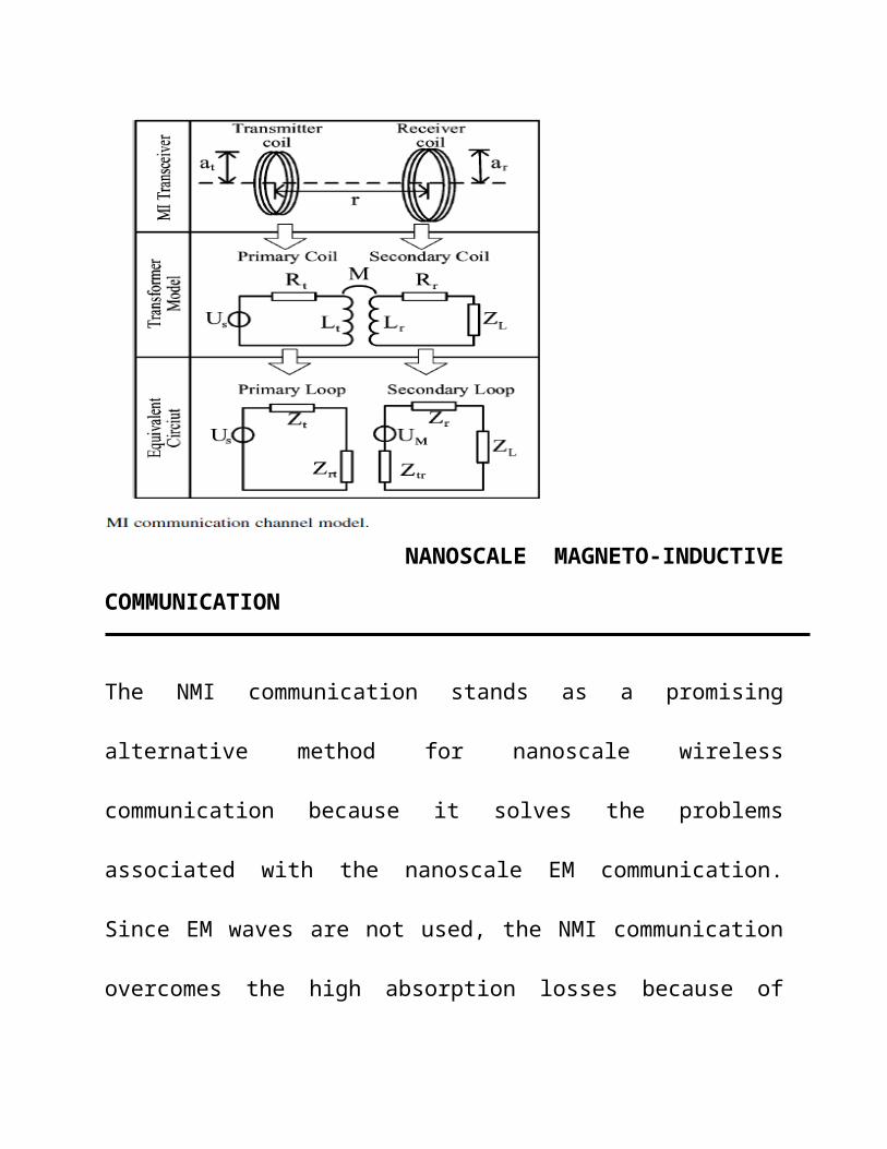
In MI communications, the transmission and reception are accomplished with
the use of a coil of wire, as shown in the firstrow in Fig. 1, where and
are the radii of the transmission coil and receiving coil, respectively; is the
distance between the transmitter and the receiver. Suppose the signal in the
transmitter coil is a sinusoidal current, i.e., where w is the
angle frequency of the transmitting signal. and is the system operating
frequency. This current can induce another sinusoidal current in the receiver
then accomplish the communication. The interaction between the two
coupled coils is represented by the mutual induction. Therefore, the MI
transmitter and receiver can be modeled as the primary coil and the
secondary coil of a transformer, respectively, as shown in the second row in
Fig. 1, where M is the mutual induction of the transmitter coil and receiver
coil; is the voltage of the transmitter’s battery; and are the self
inductions; and are the resistances of the coil; is the load
impedance of the receiver. We use its equivalent circuit to analyze the
transformer, as shown ,where
Where and are the self impedances of the transmitter coil and the
receiver coil, respectively; is the influence of the receiver on the
transmitter while is the influence of the transmitter on the receiver;
is the induced voltage on the receiver coil.
NANOSCALE MAGNETO-INDUCTIVE COMMUNICATION
The NMI communication stands as a promising alternative method for
nanoscale wireless communication because it solves the problems associated
with the nanoscale EM communication. Since EM waves are not used, the
NMI communication overcomes the high absorption losses because of
molecular absorption. Furthermore, in the NMI communication, the channel
conditions depend on the magnetic permeability of the medium. Thus, having
a communication medium with uniform permeability enables constant
channel conditions for the NMI communication. However, the point-to-point
NMI communication is a short-range nanoscale communication because the
strength of the magnetic field falls off much faster than the EM waves . That
is, whereas the molecular absorption in the NMI communication is much less
than the EM waves, the path loss of the NMI communication may be higher
than the EM communication. However, in the NMI communication, the path
loss can be reduced by forming a waveguide structure with passive relay
nodes similar to waveguides used in Magneto-Inductive (MI)
communication. To assess the performance of the point-to-point and the
waveguide NMI communication methods, we derive pathloss expressions for
both methods. The results show that using waveguide technique in the NMI
communication significantly reduces the path loss and increases feasible
communication range. Based on the numerical performance evaluation, the
NMI communication stands as a promising solution to nanoscale
communication between nanodevices. Furthermore, for nanomedicine
applications, the NMI communication can be employed in blood or tissue
liquid without having very high attenuation rates. For example, a MI
communication network is used to provide both a communication link
between implanted small devices inside the human body and a
communication link between an outer device and the implanted devices.
Moreover, in the same study, the power for the implanted devices is provided
using the MI communication.
In this paper, we first present the model of the point-to-point NMI
communication in which a single transmitter and a single receiver nanocoils
are used. Since the geometry of planar nanocoils is suitable for the
manufacturing processes of integrated circuit production, we employ planar
nanocoils in our model. The equivalent circuit of the transmitter and receiver
nanocoils is used to derive the analytical expression for the path loss in the
NMI communication channel. Using a waveguide structure greatly reduces
the path loss and increases the communication range of the MI
communication. Then, we introduce the waveguide model for the NMI
communication by employing passive relay nanonodes between the
transmitter and receiver. The analytical expression for the path loss in the
NMI communication waveguide is also obtained.
PHYSICAL MODEL OF POINT-TO-POINT NMI COMMUNICATION
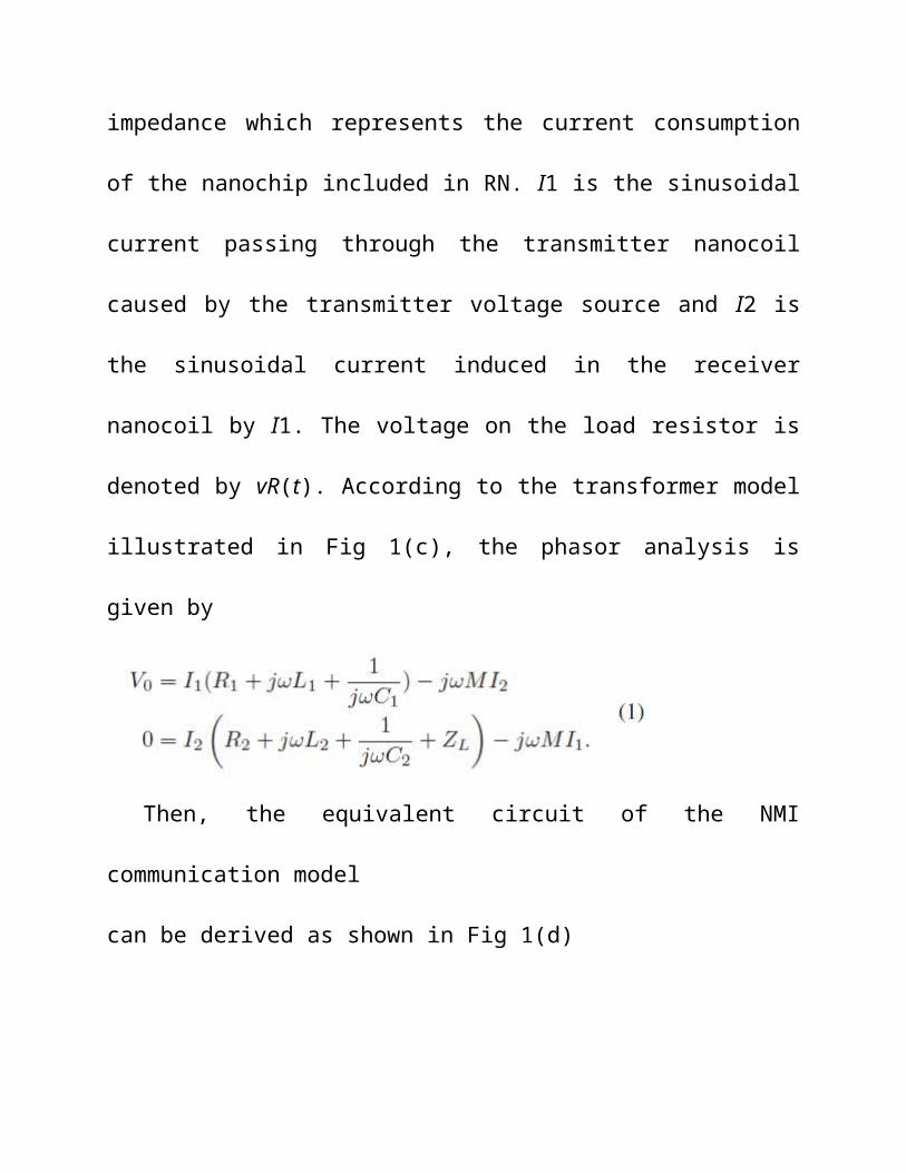
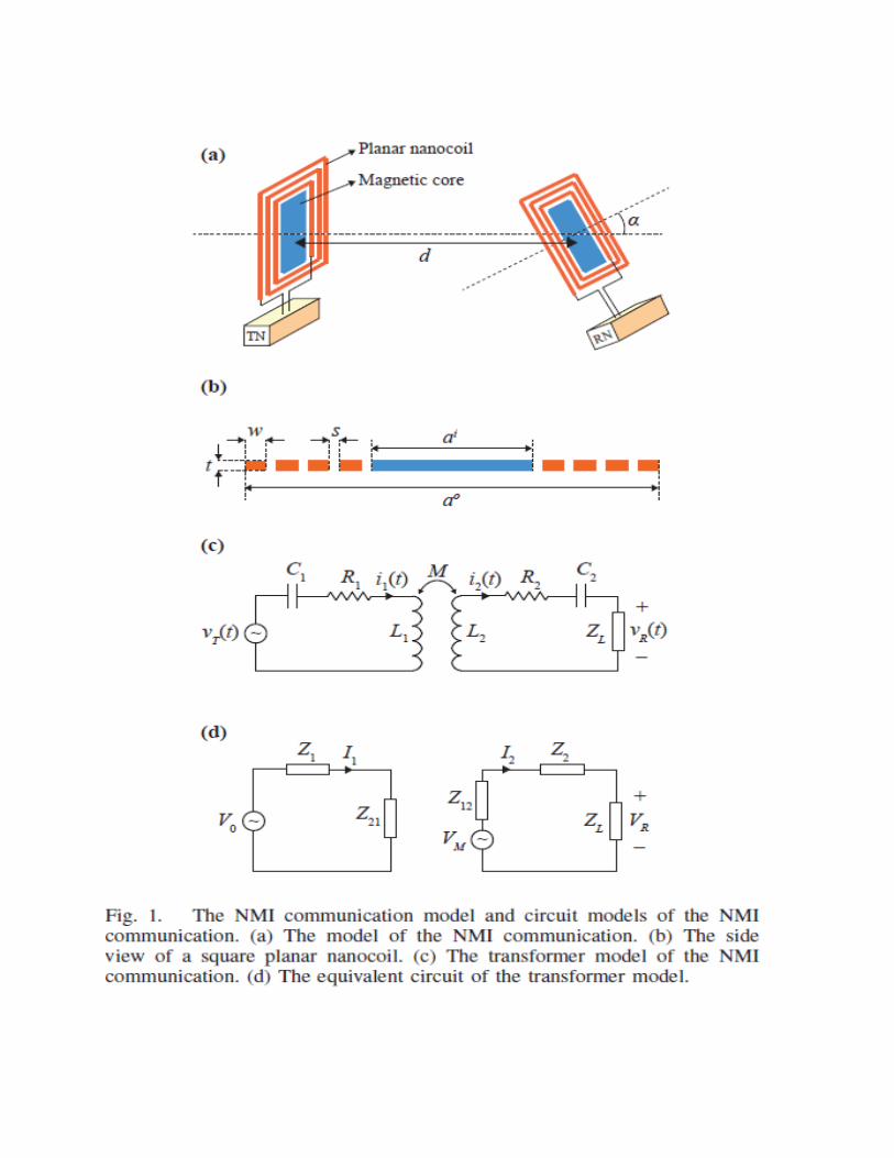
We present the physical model of the Nanoscale Magneto-Inductive (NMI)
communication between a single transmitter nanodevice (TN) and a single
receiver nanodevice (RN). In NMI communication, the information
transmission and reception is achieved using a planar nanocoil as shown in
Fig 1(a). The magnetic coupling between the transmitter and receiver
nanocoils establishes the NMI communication channel. A sinusoidal voltage
source is used in TN, i.e., vT (t) = V0 cos(ωt), where ω and V0 are the angle
frequency and amplitude of the voltage source, respectively. The sinusoidal
voltage source causes a sinusoidal current to pass through the nanocoil. This
current induces another sinusoidal current in the receiver nanocoil and it is
used to accomplish the magnetoinductive communication between TN and
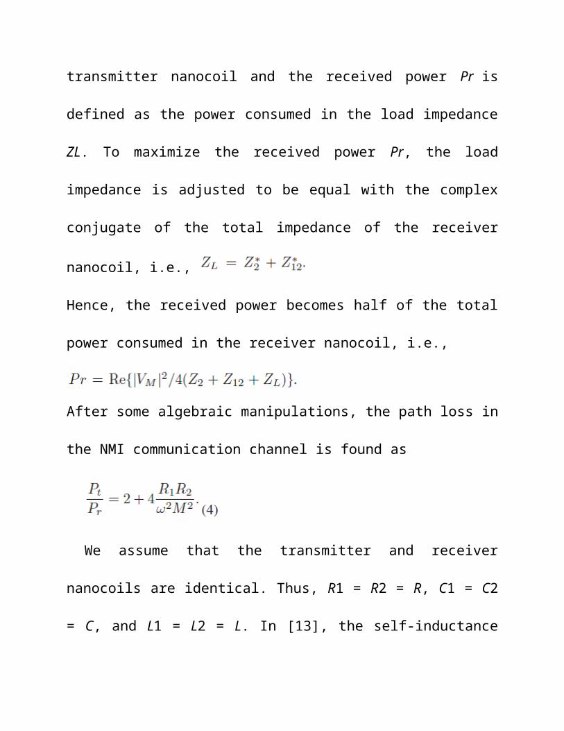
RN. In Fig 1(c), the transformer model of the NMI communication is shown.
The mutual inductance M between transmitter and receiver nanocoils
represents the coupling between these coils. L1 and L2 are the self-
inductances of the transmitter and receiver nanocoils, respectively. R1 and R2
are the resistances, and C1 and C2 are the parasitic capacitances of the
nanocoils. ZL is the load impedance which represents the current
consumption of the nanochip included in RN. I1 is the sinusoidal current
passing through the transmitter nanocoil caused by the transmitter voltage
source and I2 is the sinusoidal current induced in the receiver nanocoil by I1.
The voltage on the load resistor is denoted by vR(t). According to the
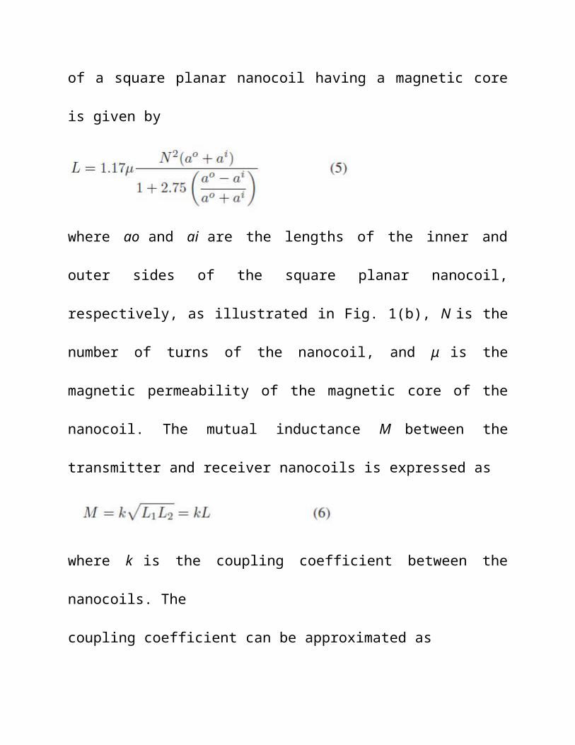
transformer model illustrated in Fig 1(c), the phasor analysis is given by
Then, the equivalent circuit of the NMI communication model
can be derived as shown in Fig 1(d)
Where,
According to the equivalent circuit of the NMI communication
model, the transmitted power, denoted by Pt, and the received
power, denoted by Pr, are given as
where Re denotes the real part. The transmitted power Pt is defined as the
power consumed in the transmitter nanocoil and the received power Pr is
defined as the power consumed in the load impedance ZL. To maximize the
received power Pr, the load impedance is adjusted to be equal with the
complex conjugate of the total impedance of the receiver nanocoil, i.e.,
Hence, the received power becomes half of the total power consumed in the
receiver nanocoil, i.e.,
After some algebraic manipulations, the path loss in the NMI communication
channel is found as
We assume that the transmitter and receiver nanocoils are identical. Thus, R1
= R2 = R, C1 = C2 = C, and L1 = L2 = L. In [13], the self-inductance of a
square planar nanocoil having a magnetic core is given by
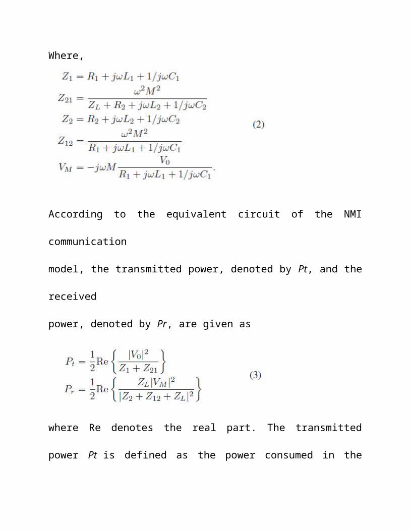
where ao and ai are the lengths of the inner and outer sides of the square
planar nanocoil, respectively, as illustrated in Fig. 1(b), N is the number of
turns of the nanocoil, and μ is the magnetic permeability of the magnetic core
of the nanocoil. The mutual inductance M between the transmitter and
receiver nanocoils is expressed as
where k is the coupling coefficient between the nanocoils. The
coupling coefficient can be approximated as
where d is the communication distance, i.e., the distance
between transmitter and receiver nanocoils, α is the angle
between the axes of the coupled coils, and aavg is the average
conductor side length of the square planar nanocoils, expressed
as a avg = (ai + ao)/2. The resistance R of the nanocoils is
found as follows
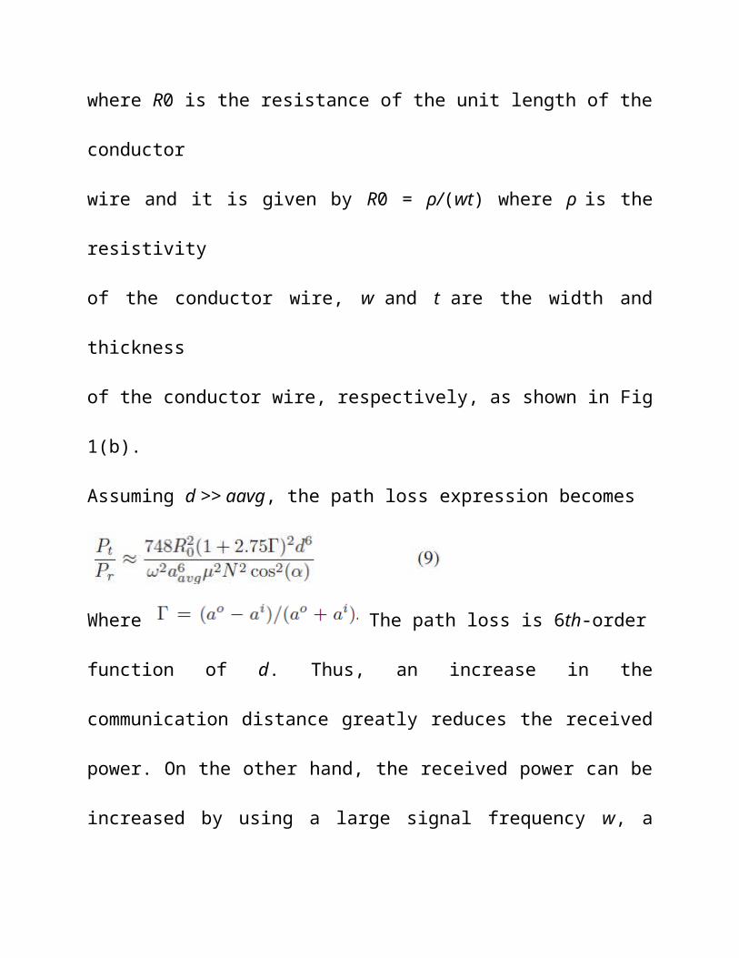
where R0 is the resistance of the unit length of the conductor
wire and it is given by R0 = ρ/(wt) where ρ is the resistivity
of the conductor wire, w and t are the width and thickness
of the conductor wire, respectively, as shown in Fig 1(b).
Assuming d >> aavg, the path loss expression becomes

Where The path loss is 6th-order
function of d. Thus, an increase in the communication distance greatly
reduces the received power. On the other hand, the received power can be
increased by using a large signal frequency w, a large number of turns N, a
large averagenanocoil side length aavg, a large permeability of the magnetic
core μ, and a small unit length resistance R0.
WAVEGUIDE MODEL FOR NMI COMMUNICATION
In the previous section, the NMI communication channel was modeled for a
point-to-point communication network. In the NMI communication, the
received power falls off proportionally with d^−6 in (9). Therefore, the
communication distance d has a severe effect on the received power and this
effect limits the NMI communication range. In this section, to increase the
range of the NMI communication, we employ relay nanonodes between the
transmitter and receiver nanocoils to form a magneto-inductive waveguide.
For the NMI communication, the relay nanonodes are assumed to be passive
devices; that is, a relay nanonode includes only a nanocoil and does not have
a power source or processing circuitry. The signal propagation through the
relay nanonodes is achieved by the magnetic coupling between nanocoils.
That is, the sinusoidal current passing in the transmitter nanocoil induces a
sinusoidal current in the nanocoil of the first relay nanonode. Then, the
induced sinusoidal current in the first relay nanocoil also induces a sinusoidal
current in the second relay nanocoil and the transmitted signal propagates in a
similar manner until the induced current reaches the receiver nanodevice.
The waveguide model for the NMI communication is shown in Fig. 2(a). In
the waveguide, there are n nanocoils equally spaced including the nanocoils
in the transmitter and receiver nanodevices. Therefore, if the distance
between transmitter and receiver nanocoils is r, the distance between two
successive nanocoil is given by d = r/(n − 1). Furthermore, we assume that
only the adjacent nanocoils are magnetically coupled; hence, we only use the
mutual inductance between the adjacent nanocoils. The multi-stage
transformer model for the NMI communication waveguide is demonstrated in
Fig 2(b).
The nanocoils in all nodes are assumed to be identical, and L, M, and R are
given in (5), (6), and (8), respectively.
The equivalent circuit for the transmitter and receiver nanocoils can be seen
in Fig 2(c) where
where Zij denotes the reflected impedance of the ith nanocoil into the jth
nanocoil, and VMi denotes the induced voltage on the ith nanocoil. According
to the equivalent circuit of the NMI communication waveguide, the
transmitted power Pt and the received power Pr are expressed as
To maximize the received power, the angle frequency of the transmitted
signal is chosen the same as the resonant frequency of the equivalent RLC
circuit of the planar nanocoil. The resonant frequency of the nanocoil is

given as and hence jω0L + (1/jω0C) = 0. Therefore, the
impedance of a nanocoil becomes Z = R and the path loss in the NMI
communication waveguide is given by
Where,
And and Since the expression in
(12) is too complicated to simplify, the effect of the communication distance
r on the path loss in the waveguide is analyzed numerically in the next
section.
PERFORMANCE EVALUATION
In this section, we present the numerical performance analysis of both the
point-to-point NMI communication and the NMI communication waveguide.
The path loss, i.e., (Pt/Pr), is used as the performance criterion and evaluated
with respect to the communication distance for different magnetic
permeabilities of the magnetic cores in the nanocoils.
We use MATLAB to perform the performance analysis. The path loss
expressions for the point-to-point NMI communication and the NMI
communication waveguide are given in (9) and (12), respectively.
For the dimensions of a nanocoil, we use ao = 500nm, w = 40nm, s = 1nm, t
= 40nm, with N = 5 turns and α = 0◦. For the numerical analysis, we consider
the conductor wire as copper whose resistivity is ρ = 1.68 × 10⁻⁸Ωm.
Furthermore, the angle frequency of the signal source is assumed to
where L is given in (5) and the capacitance is C = 0.01fF.
For the point-to-point NMI communication, the path loss in dB with respect
to the communication distance d for different relative magnetic permeabilities
μr is illustrated in Fig. 3. The relative magnetic permeability is defined as μr
= μ/μ0 where μ0 is the magnetic permeability of free space. The path loss
increases with an increase in the communication distance as seen in (9) and in
Fig. 3. For example, for μr = 1000, the path loss is 63.4dB at d = 10μm and
the path loss is 123.0dB at d = 100μm. As the communication distance
increases, first, the path loss exhibits a fast increase and then, it slowly
increases. As a result, considering the power limitation of the nanodevices,
the practical communication range of the point to-point NMI commn is short.
According to the results shown in Fig. 3, a decrease in the relative
permeability μr increases the path loss, which also can be seen in (9).
For d ≥ 5μm, decreasing μr from 1000 to 300 increases the path loss by 5dB.
Therefore, using a magnetic core with large permeability in the nanocoil
improves the achievable communication range of the NMI communication
by decreasing the path loss. For the NMI waveguide communication, the path
loss in dB with respect to the communication distance between transmitter
and receiver r for different relative magnetic permeabilities μr is
demonstrated in Fig. 4. In this analysis, the distance between adjacent coils is
constant and given by d = ao/2. The communication distance is increased by
increasing the number of relay coils in the waveguide. In addition, the relay
coils in the waveguide do not require any power. The results show that an
increase in the communication distance increases the path loss. For instance,
for μr = 1000, the path loss is 3.3dB at r = 10μm and the path loss is 19.0dB
at r = 100μm. Note that, for the same communication distances, the
waveguide technique greatly reduces the path loss compared with the point-
to-point NMI communication.
Although the path loss in dB abruptly increases in the point to- point NMI
communication as the communication distance increases, in the NMI
waveguide, the path loss in dB increases linearly with a small slope compared
with the point-to-point case. Thus, by using the waveguide technique, the
range of the NMI communication is significantly increased. Based on
the results, the NMI waveguide communication stands as a promising
solution to long range nanoscale communication. The numerical results given
in Fig. 4 show that, for the NMI waveguide communication, a decrease in the
relative permeability μr increases the path loss. As the communication

distance increases, the difference between the path loss values for μr = 300
and μr = 1000 increases. Even though for d = 20μm, decreasing μr from 1000
to 300 increases the path loss by 2.8dB, for d = 100μm, decreasing μr from
1000 to 300 increases the path loss by 15.7dB. Hence, a large permeability of
the core in the nanocoil significantly improves the feasible communication
range of the NMI communication by decreasing the path loss.
CONCLUSION
In this paper, we propose a novel nanoscale communication technique, i.e.,
the NMI communication which relies on the magnetic coupling between
nanocoils. We present a realistic physical communication model for both the
point-to-point and waveguide NMI communication methods. Then, we derive
the closed-form expression of the path loss for both techniques. The
numerical analyses show that using waveguide method in the NMI
communication can significantly reduce the path loss and increase the
achievable communication range of the NMI communication. Since the relay
coils used in the waveguide do not require power, a single passive nanocoil
can serve as a relay nanonode. In addition, using a magnetic core in the
nanocoils with large permeability also decreases the path loss in the NMI
communication. The problems that EM waves encounter at nanoscale are
high attenuation rates due to high molecular absorption and frequency
selective channel characteristics. The novel NMI communication overcomes
these problems by introducing low absorption losses and flat channel
characteristics. Although the path loss is more severe in the NMI
communication than in Nanoscale EM communication, using the waveguide
NMI communication method solves the high path loss problem in the NMI
communication. Therefore, the NMI communication stands as a promising
alternative wireless nanoscale communication technique.

REFERENCES
IEEE REFERENCES
Nanoscale Magneto-Inductive communication
Kilinc, D. ; Akan, O.B.
Signals, Systems and Computers, 2013 Asilomar Conference on
DOI: 10.1109/ACSSC.2013.6810454
Publication Year: 2013 , Page(s): 1061 – 1065
Z. Sun and I. Akyildiz, “Magnetic induction communications for wireless
underground sensor networks,” IEEE Transactions on Antenna and
Propagation, vol. 58, no. 7, pp. 2426-2435, July 2010.
F. Akyildiz, F. Brunetti, C. Blazquez, “Nanonetworks: A new communication
paradigm,” Computer Networks (Elsevier), vol. 52, no. 12, pp.
2260-2279, 2008.
F. Akyildiz, J. M. Jornet, and M. Pierobon,“Propagation Models
for Nanocommunication Networks,” in Proc. of EUCAP 2010, Fourth
European Conference on Antennas and Propagation, April 2010, pp.
4229-4232.
ONLINE REFERENCES
Nanotechnology, http://en.wikipedia.org/wiki/Nanotechnology
Nanonetwork, http://en.wikipedia.org/wiki/Nanonetwork
Nanoscale Communication With Molecular Arrays in Nanonetworks
Atakan, B. ; Galmes, S. ; Akan, O.B.
NanoBioscience, IEEE Transactions on
Volume: 11 , Issue: 2
Near-field magnetic induction communication, http://en.wikipedia.org/wiki/Near-
field_magnetic_induction_communication
MagnetoInductiveTechnology.
http://www.roboticstomorrow.com/article/2012/09/magneto-inductive-communication-
interview-with-steve-parsons-ultra-electronics/81/