business division - orange coast...
TRANSCRIPT
Orange Coast CollegeBusiness Division
Computer Science Department
CS 116- Computer Architecture
Logic Design: Part the Last
OCC - CS/CIS CS116-Ch00-Orientation 21998 Morgan Kaufmann Publishers ( Augmented & Modif ied by M.Malaty) 2OCC-CS 116 Fall 2003 1998 Morgan Kaufmann Publishers (Augmented & Modified by M.Malaty and M. Beers)
Sequential Circuits
• Circuits with memory• Outputs depend on:
– past sequence
– possibly the input
• Represented with state diagrams or tables

OCC - CS/CIS CS116-Ch00-Orientation 31998 Morgan Kaufmann Publishers ( Augmented & Modif ied by M.Malaty) 3OCC-CS 116 Fall 2003 1998 Morgan Kaufmann Publishers (Augmented & Modified by M.Malaty and M. Beers)
State Stuff
• State (Transition) diagram:– Circles represent states – Directed line segments represent transitions
between the states. – One or more actions (outputs) may be associated
with each transition. – Represents a finite state machine.
• Finite state machine:– A function which maps an ordered sequence of
input events into a corresponding sequence of (sets of) output events
OCC - CS/CIS CS116-Ch00-Orientation 41998 Morgan Kaufmann Publishers ( Augmented & Modif ied by M.Malaty) 4OCC-CS 116 Fall 2003 1998 Morgan Kaufmann Publishers (Augmented & Modified by M.Malaty and M. Beers)
State Diagram Examples
• Insert pics?– Special counter: http://www.utdallas.edu/~frankd
/SD1.html– Toaster:
http://odl-skopje.etf.ukim.edu.mk/UML-Help/html/03day3.html– Invoice:
http://www.dcs.warwick.ac.uk/~ananda/lnotes/node278.html– Multiprocesor system:
http://www.dca.fee.unicamp.br/~leopini/private/sib98/sld037.htm– T-Flip-flop:
http://ranger.uta.edu/~carroll/cse2341/spring99/chapter8/sld015.htm

OCC - CS/CIS CS116-Ch00-Orientation 51998 Morgan Kaufmann Publishers ( Augmented & Modif ied by M.Malaty) 5OCC-CS 116 Fall 2003 1998 Morgan Kaufmann Publishers (Augmented & Modified by M.Malaty and M. Beers)
Sequential Circut Models
• Mealy machine– Output depends on both input & current state
– Output changes whenever input changes
InputNext state
logicState
memoryOutput logic
Clock
Excitation
Output

OCC - CS/CIS CS116-Ch00-Orientation 61998 Morgan Kaufmann Publishers ( Augmented & Modif ied by M.Malaty) 6OCC-CS 116 Fall 2003 1998 Morgan Kaufmann Publishers (Augmented & Modified by M.Malaty and M. Beers)
Sequential Circuit Examples● State diagram for Mealy machine

OCC - CS/CIS CS116-Ch00-Orientation 71998 Morgan Kaufmann Publishers ( Augmented & Modif ied by M.Malaty) 7OCC-CS 116 Fall 2003 1998 Morgan Kaufmann Publishers (Augmented & Modified by M.Malaty and M. Beers)
Sequential Circut Models
• Moore machine– Output depends on current state only
– Output changes after clock edge
InputNext state
logicState
memoryOutput logic
Clock
Excitation
Output

OCC - CS/CIS CS116-Ch00-Orientation 81998 Morgan Kaufmann Publishers ( Augmented & Modif ied by M.Malaty) 8OCC-CS 116 Fall 2003 1998 Morgan Kaufmann Publishers (Augmented & Modified by M.Malaty and M. Beers)
Moore Machine State Diagram● State diagram for Moore machine

OCC - CS/CIS CS116-Ch00-Orientation 91998 Morgan Kaufmann Publishers ( Augmented & Modif ied by M.Malaty) 9OCC-CS 116 Fall 2003 1998 Morgan Kaufmann Publishers (Augmented & Modified by M.Malaty and M. Beers)
Memory Elements
• Memory element:– Stores values
– Controlled usually by clock
– Can be static or dynamic, volatile or non-volatile

OCC - CS/CIS CS116-Ch00-Orientation 101998 Morgan Kaufmann Publishers ( Augmented & Modif ied by M.Malaty) 10OCC-CS 116 Fall 2003 1998 Morgan Kaufmann Publishers (Augmented & Modified by M.Malaty and M. Beers)
Clocks
• Relative execution times of instructions on a computer are usually measured by number of clock cycles rather than seconds.
• Clock rates for various models of the computer may increase as technology improves
• Definitions:– A free-running signal with a fixed cycle time.
– A processor's clock or one cycle thereof.

OCC - CS/CIS CS116-Ch00-Orientation 111998 Morgan Kaufmann Publishers ( Augmented & Modif ied by M.Malaty) 11OCC-CS 116 Fall 2003 1998 Morgan Kaufmann Publishers (Augmented & Modified by M.Malaty and M. Beers)
• Synchronous system: – A system in which state changes only occur in
specific time controlled by a free-running clock.
• Asynchronous system:– A system in which state changes occur according
to some other events.
• Clock cycle time (period/interval):– The time between successive transitions in the
same direction, i.e. a complete period in which the signal has one high and one low signal levels.
Clock Systems

OCC - CS/CIS CS116-Ch00-Orientation 121998 Morgan Kaufmann Publishers ( Augmented & Modif ied by M.Malaty) 12OCC-CS 116 Fall 2003 1998 Morgan Kaufmann Publishers (Augmented & Modified by M.Malaty and M. Beers)
Clock Definitions• Duty cycle: The percentage that the clock signal is at its asserted
level.
• Clock frequency: The inverse of the cycle time.
• Edge-triggered clocking: State changes occur on a clock edge.
• Rising edge: The edge that converts the signal from low to high.
• Falling edge:The edge that converts the signal from high to low.
• Set-up time: The minimum time that the input must be valid before the clock edge.
• Hold time: The minimum time during which the input must be valid after the clock edge.
Rising Edge
Falling Edge
Clock CycleA clock signal oscillates between high & low values

OCC - CS/CIS CS116-Ch00-Orientation 131998 Morgan Kaufmann Publishers ( Augmented & Modif ied by M.Malaty) 13OCC-CS 116 Fall 2003 1998 Morgan Kaufmann Publishers (Augmented & Modified by M.Malaty and M. Beers)
Clocks• Clock edge determines when contents of state elements
are updated
– Cycle must be long enough for input values to stabilize.
– Edge triggered clocking preferred because a state element can be used as both input and output to the same logic circuit.
• Clocks are needed in sequential logic to decide when an element that contains a state should be updated.
• Must have enough period that allows all signals to stabilize.
C lo c k cy cle
S ta tee le m e n t
1C o m b in a tio n al lo gi c
S ta tee le m e nt
2
OCC - CS/CIS CS116-Ch00-Orientation 141998 Morgan Kaufmann Publishers ( Augmented & Modif ied by M.Malaty) 14OCC-CS 116 Fall 2003 1998 Morgan Kaufmann Publishers (Augmented & Modified by M.Malaty and M. Beers)
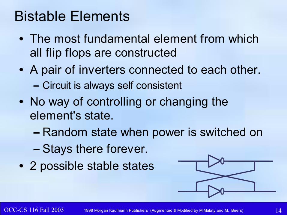
Bistable Elements
• The most fundamental element from which all flip flops are constructed
• A pair of inverters connected to each other. – Circuit is always self consistent
• No way of controlling or changing the element's state.
– Random state when power is switched on
– Stays there forever.
• 2 possible stable states

OCC - CS/CIS CS116-Ch00-Orientation 151998 Morgan Kaufmann Publishers ( Augmented & Modif ied by M.Malaty) 15OCC-CS 116 Fall 2003 1998 Morgan Kaufmann Publishers (Augmented & Modified by M.Malaty and M. Beers)
Latch
• Used to store 1 or more bits– Has a data input and an output
– Input is latched (stored)
– Transferred to output• Output retains value until next clock cycle
OCC - CS/CIS CS116-Ch00-Orientation 161998 Morgan Kaufmann Publishers ( Augmented & Modif ied by M.Malaty) 16OCC-CS 116 Fall 2003 1998 Morgan Kaufmann Publishers (Augmented & Modified by M.Malaty and M. Beers)
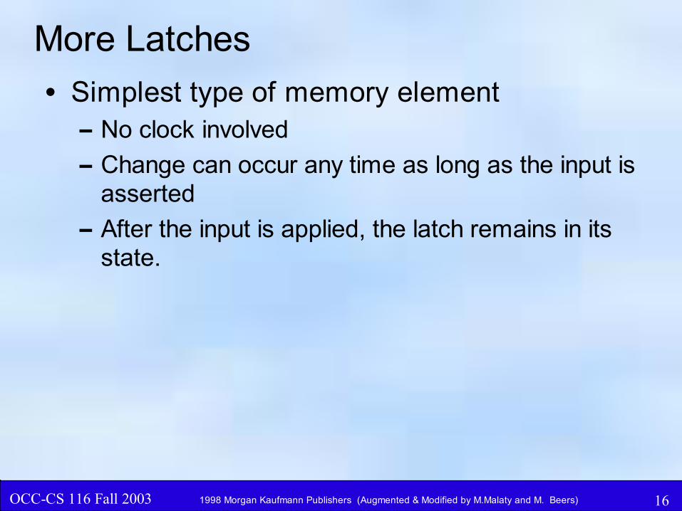
More Latches
• Simplest type of memory element– No clock involved
– Change can occur any time as long as the input is asserted
– After the input is applied, the latch remains in its state.

OCC - CS/CIS CS116-Ch00-Orientation 171998 Morgan Kaufmann Publishers ( Augmented & Modif ied by M.Malaty) 17OCC-CS 116 Fall 2003 1998 Morgan Kaufmann Publishers (Augmented & Modified by M.Malaty and M. Beers)
Flip Flop (FF)
• Can be in one of two states– Toggles between based on inputs
– Essentially a 1 bit memory
• Common types– SR flip-flop
– JK flip-flop
– D-Type flip-flop (latch)
– T flip-flop

OCC - CS/CIS CS116-Ch00-Orientation 181998 Morgan Kaufmann Publishers ( Augmented & Modif ied by M.Malaty) 18OCC-CS 116 Fall 2003 1998 Morgan Kaufmann Publishers (Augmented & Modified by M.Malaty and M. Beers)
More flip-flops
• Non-transparent
• Reading input and generating output are separate events
• Changes occur only at a clock edge
• Flip-Flop’s and latches are the basic building blocks of most sequential circuits. Their function is to store signals

OCC - CS/CIS CS116-Ch00-Orientation 191998 Morgan Kaufmann Publishers ( Augmented & Modif ied by M.Malaty) 19OCC-CS 116 Fall 2003 1998 Morgan Kaufmann Publishers (Augmented & Modified by M.Malaty and M. Beers)
Set-Reset (S-R) Latches
• Built from a pair of NOR or NAND gates.
• Two-Inputs:– S for set & R for reset.
• Two-Outputs:– Q output & Q' (inverted output).
Q’Q1110010110??00Q’QRS Undefined
Set state
Reset sate
Unchanged
Q
_Q
S
R
Implementation Using NANDs
??1101011010Q’Q00Q’QRS Unchanged
Set state
Reset sate
Undefined
Q
_Q
R
S
Implementation Using NORs

OCC - CS/CIS CS116-Ch00-Orientation 201998 Morgan Kaufmann Publishers ( Augmented & Modif ied by M.Malaty) 20OCC-CS 116 Fall 2003 1998 Morgan Kaufmann Publishers (Augmented & Modified by M.Malaty and M. Beers)
Set-Reset Latches
• What happens on different inputs?– Only S is asserted
• Latch is set to the state (Q=1 and Q'=0).
– Only R is asserted• Latch is reset to the state(Q=0 and Q'=1).
– Both S &R are not asserted• Latch stays in its current state.
– If both S and R are asserted • Undefined AND Dangerous !!
• Circuit behaves like a bistable element.– Can lead to incorrect operation or oscillate in an
unstable state.
OCC - CS/CIS CS116-Ch00-Orientation 211998 Morgan Kaufmann Publishers ( Augmented & Modif ied by M.Malaty) 21OCC-CS 116 Fall 2003 1998 Morgan Kaufmann Publishers (Augmented & Modified by M.Malaty and M. Beers)
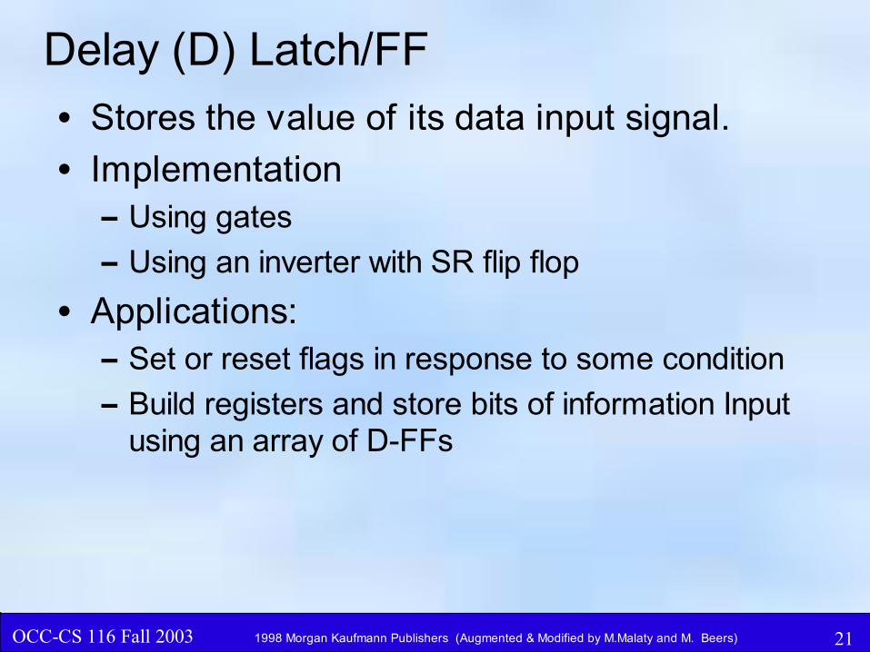
Delay (D) Latch/FF
• Stores the value of its data input signal.
• Implementation– Using gates
– Using an inverter with SR flip flop
• Applications:– Set or reset flags in response to some condition
– Build registers and store bits of information Input using an array of D-FFs

OCC - CS/CIS CS116-Ch00-Orientation 221998 Morgan Kaufmann Publishers ( Augmented & Modif ied by M.Malaty) 22OCC-CS 116 Fall 2003 1998 Morgan Kaufmann Publishers (Augmented & Modified by M.Malaty and M. Beers)
Delay/Flip-Flop
• Output:– The value of the internal state (Q)
– Complement of internal state (Q')
• When the input is – Asserted
• Latch is open and the value of the output becomes the value of the input.
– Deasserted:• Latch is closed and the output holds its value.

OCC - CS/CIS CS116-Ch00-Orientation 231998 Morgan Kaufmann Publishers ( Augmented & Modif ied by M.Malaty) 23OCC-CS 116 Fall 2003 1998 Morgan Kaufmann Publishers (Augmented & Modified by M.Malaty and M. Beers)
Closer look at Delay Flip-flops
QC
DQ Q’QX0
01111001Q’QDClock
Truth table
D
C
QOperation of a D-latch
Assumption: output initially deasserted
OCC - CS/CIS CS116-Ch00-Orientation 241998 Morgan Kaufmann Publishers ( Augmented & Modif ied by M.Malaty) 24OCC-CS 116 Fall 2003 1998 Morgan Kaufmann Publishers (Augmented & Modified by M.Malaty and M. Beers)
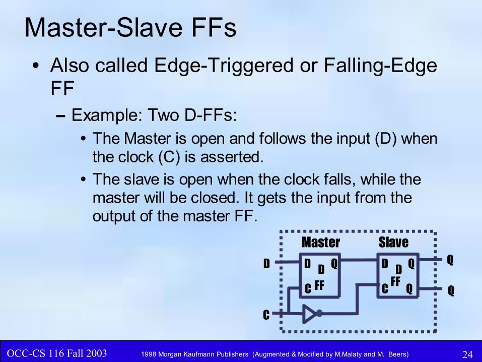
Master-Slave FFs• Also called Edge-Triggered or Falling-Edge
FF– Example: Two D-FFs:
• The Master is open and follows the input (D) when the clock (C) is asserted.
• The slave is open when the clock falls, while the master will be closed. It gets the input from the output of the master FF.
QQ QD
FFD
C
DDD
C
C
FF
Master Slave

OCC - CS/CIS CS116-Ch00-Orientation 251998 Morgan Kaufmann Publishers ( Augmented & Modif ied by M.Malaty) 25OCC-CS 116 Fall 2003 1998 Morgan Kaufmann Publishers (Augmented & Modified by M.Malaty and M. Beers)
Master-Slave Flip-flops
• During each clock period at most one state change will take place– Race conditions is avoided
• Especially useful when input of a FF is a function of its own output
• We can also have Master-Slave S-R or J-K FFs
D
C
Q
Operation of a D-FF with a falling edge trigger, assuming the
output is initially deasserted

OCC - CS/CIS CS116-Ch00-Orientation 261998 Morgan Kaufmann Publishers ( Augmented & Modif ied by M.Malaty) 26OCC-CS 116 Fall 2003 1998 Morgan Kaufmann Publishers (Augmented & Modified by M.Malaty and M. Beers)
Master-Slave FFs• Race Conditions:
– Multiple variables change state due to a single input changing state
– Non-critical racing• Exactly one final state is reached regardless of the
order and speed of internal variable changes
– Critical racing:• Two or more final states could be reached
• Depends on the order and speed of the internal variable changes
• Critical racing should be avoided– The behavior of the circuit cannot be predicted

OCC - CS/CIS CS116-Ch00-Orientation 271998 Morgan Kaufmann Publishers ( Augmented & Modif ied by M.Malaty) 27OCC-CS 116 Fall 2003 1998 Morgan Kaufmann Publishers (Augmented & Modified by M.Malaty and M. Beers)
Other Flip-Flops• J-K-FFs
– A modified SR flip-flop– Prevents both inputs from
being assigned 1 simultaneously
• T-FFs – A single-input JK flip-flop– Both inputs are tied
together– The output toggles
whenever input is applied
QK
J
ClockQ
QT
_
QClock

OCC - CS/CIS CS116-Ch00-Orientation 281998 Morgan Kaufmann Publishers ( Augmented & Modif ied by M.Malaty) 28OCC-CS 116 Fall 2003 1998 Morgan Kaufmann Publishers (Augmented & Modified by M.Malaty and M. Beers)
Characteristics Tables of FFs
q’(T) Complement11
1 Set01
0 Reset10
q(T) No change00
Q[t+1)KJ
J-K FF S-R FF
? Unpredictable11
1 Set01
0 Reset10
q(T) No change00
Q[t+1)RS
Set1
Reset0
Q[t+1)D
D FF
Q’(t) Complement1
Q(t) No change0
Q[t+1)T
T FF

OCC - CS/CIS CS116-Ch00-Orientation 291998 Morgan Kaufmann Publishers ( Augmented & Modif ied by M.Malaty) 29OCC-CS 116 Fall 2003 1998 Morgan Kaufmann Publishers (Augmented & Modified by M.Malaty and M. Beers)
Excitation Tables of FFs
0X11
1001
0110
X000
RSQ(t+1)Q(t)
S-R FF
0X11
1X01
X110
X000
KJQ(t+1)Q(t)
J-K FF
D FF
111
001
110
000
DQ(t+1)Q(t)
T FF
011
101
110
000
TQ(t+1)Q(t)

OCC - CS/CIS CS116-Ch00-Orientation 301998 Morgan Kaufmann Publishers ( Augmented & Modif ied by M.Malaty) 30OCC-CS 116 Fall 2003 1998 Morgan Kaufmann Publishers (Augmented & Modified by M.Malaty and M. Beers)
Sequential Circuits Design Steps• State the description of the circuit behavior,
– State diagram, timing diagram, etc.
• Obtain the state table.– Reduce the number of states
– Assign binary value to each state.
• Determine the number of FFs needed for the state combination.– Choose the type of the FFs used.

OCC - CS/CIS CS116-Ch00-Orientation 311998 Morgan Kaufmann Publishers ( Augmented & Modif ied by M.Malaty) 31OCC-CS 116 Fall 2003 1998 Morgan Kaufmann Publishers (Augmented & Modified by M.Malaty and M. Beers)
Designing a circuit Part 2
• From the state table, derive the excitation table.– Derive the circuit output functions and FFs input
functions, • Karnaugh map, or any other simplification method.
• Draw the logic diagram.

OCC - CS/CIS CS116-Ch00-Orientation 321998 Morgan Kaufmann Publishers ( Augmented & Modif ied by M.Malaty) 32OCC-CS 116 Fall 2003 1998 Morgan Kaufmann Publishers (Augmented & Modified by M.Malaty and M. Beers)
Sequential Circuits Analysis Steps
• Determine the value of the input function, – In terms of the present state and input variables
– For each flip-flop in the circuit.
• Use the flip-flop characteristics table to determine the next state.
• Build the State table– Use information known
• Use columns indicating the present state, input, next state, and output.
• Draw the state diagram
OCC - CS/CIS CS116-Ch00-Orientation 331998 Morgan Kaufmann Publishers ( Augmented & Modif ied by M.Malaty) 33OCC-CS 116 Fall 2003 1998 Morgan Kaufmann Publishers (Augmented & Modified by M.Malaty and M. Beers)
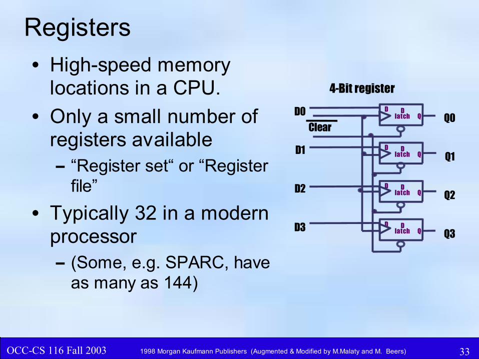
Registers
• High-speed memory locations in a CPU.
• Only a small number of registers available– “Register set“ or “Register
file”
• Typically 32 in a modern processor – (Some, e.g. SPARC, have
as many as 144)
4-Bit register
Dlatch Q
D
Dlatch Q
D
Dlatch Q
D
Dlatch Q
D
D0
D1
D2
D3
ClearQ0
Q1
Q2
Q3
OCC - CS/CIS CS116-Ch00-Orientation 341998 Morgan Kaufmann Publishers ( Augmented & Modif ied by M.Malaty) 34OCC-CS 116 Fall 2003 1998 Morgan Kaufmann Publishers (Augmented & Modified by M.Malaty and M. Beers)
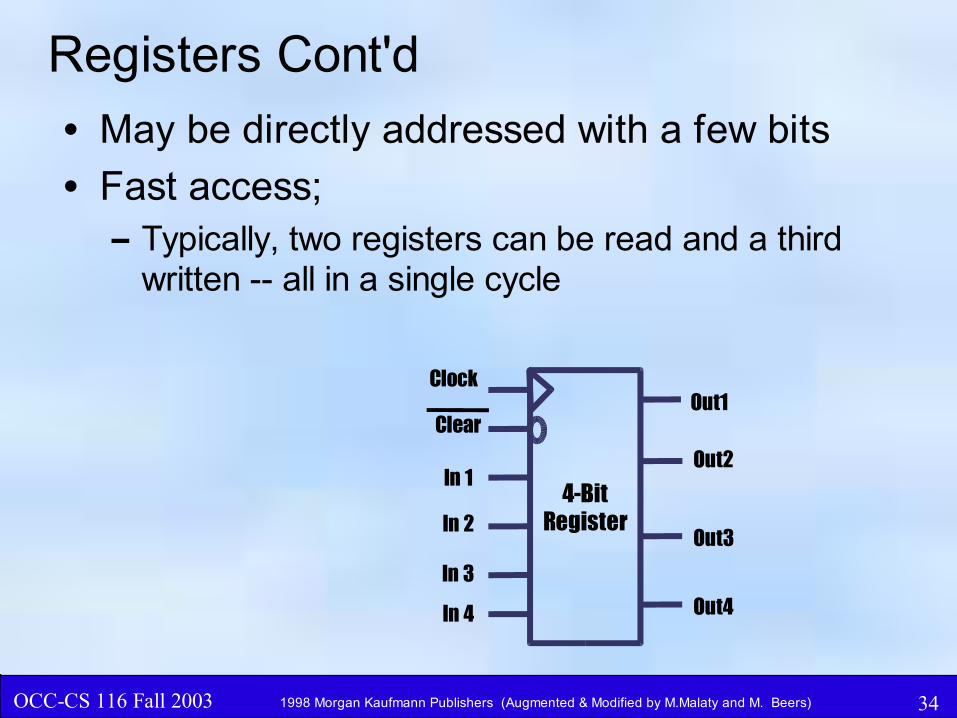
Registers Cont'd
• May be directly addressed with a few bits
• Fast access; – Typically, two registers can be read and a third
written -- all in a single cycle
4-BitRegister
In 1
Clock
ClearOut1
Out2
Out3
Out4In 4
In 3
In 2
OCC - CS/CIS CS116-Ch00-Orientation 351998 Morgan Kaufmann Publishers ( Augmented & Modif ied by M.Malaty) 35OCC-CS 116 Fall 2003 1998 Morgan Kaufmann Publishers (Augmented & Modified by M.Malaty and M. Beers)
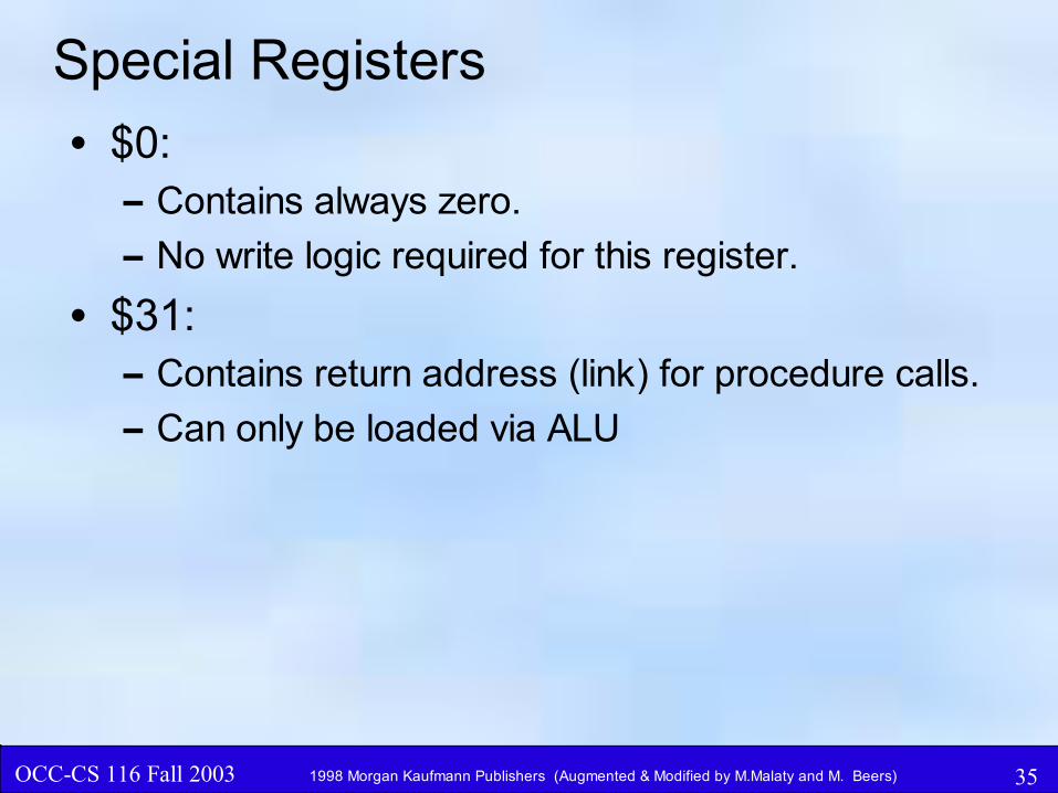
Special Registers
• $0: – Contains always zero.
– No write logic required for this register.
• $31: – Contains return address (link) for procedure calls.
– Can only be loaded via ALU
OCC - CS/CIS CS116-Ch00-Orientation 361998 Morgan Kaufmann Publishers ( Augmented & Modif ied by M.Malaty) 36OCC-CS 116 Fall 2003 1998 Morgan Kaufmann Publishers (Augmented & Modified by M.Malaty and M. Beers)
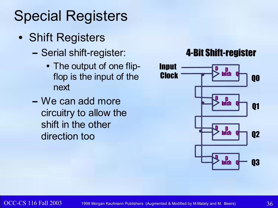
Special Registers
• Shift Registers– Serial shift-register:
• The output of one flip-flop is the input of the next
– We can add more circuitry to allow the shift in the other direction too
InputClock
Dlatch Q
D
Dlatch Q
D
Dlatch Q
D
Dlatch Q
D
Q0
Q1
Q2
Q3
4-Bit Shift-register
OCC - CS/CIS CS116-Ch00-Orientation 371998 Morgan Kaufmann Publishers ( Augmented & Modif ied by M.Malaty) 37OCC-CS 116 Fall 2003 1998 Morgan Kaufmann Publishers (Augmented & Modified by M.Malaty and M. Beers)
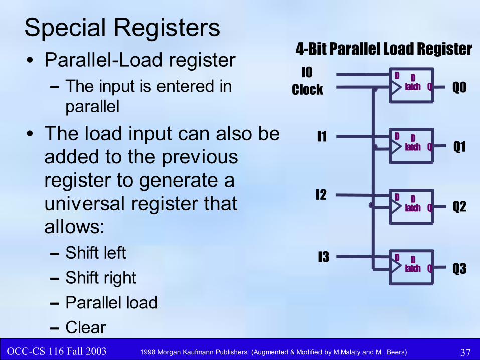
Special Registers• Parallel-Load register
– The input is entered in parallel
• The load input can also be added to the previous register to generate a universal register that allows:
– Shift left
– Shift right
– Parallel load
– Clear
I0Clock
Dlatch Q
D
Dlatch Q
D
Dlatch Q
D
Dlatch Q
D
Q0
4-Bit Parallel Load Register
I3
I2
I1Q1
Q2
Q3
OCC - CS/CIS CS116-Ch00-Orientation 381998 Morgan Kaufmann Publishers ( Augmented & Modif ied by M.Malaty) 38OCC-CS 116 Fall 2003 1998 Morgan Kaufmann Publishers (Augmented & Modified by M.Malaty and M. Beers)
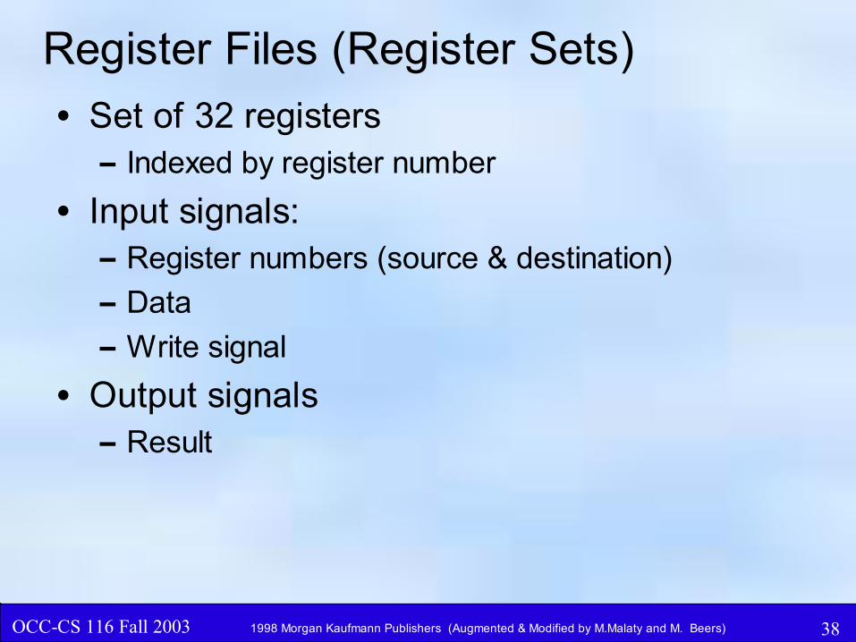
Register Files (Register Sets)
• Set of 32 registers – Indexed by register number
• Input signals:– Register numbers (source & destination)
– Data
– Write signal
• Output signals– Result
OCC - CS/CIS CS116-Ch00-Orientation 391998 Morgan Kaufmann Publishers ( Augmented & Modif ied by M.Malaty) 39OCC-CS 116 Fall 2003 1998 Morgan Kaufmann Publishers (Augmented & Modified by M.Malaty and M. Beers)
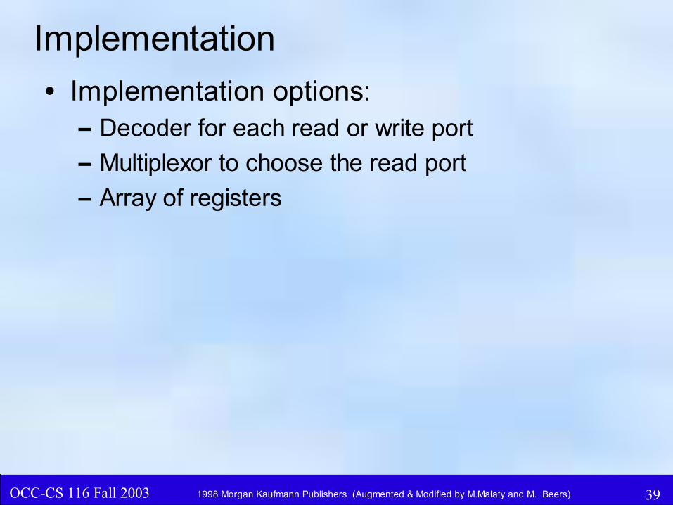
Implementation
• Implementation options:– Decoder for each read or write port
– Multiplexor to choose the read port
– Array of registers

OCC - CS/CIS CS116-Ch00-Orientation 401998 Morgan Kaufmann Publishers ( Augmented & Modif ied by M.Malaty) 40OCC-CS 116 Fall 2003 1998 Morgan Kaufmann Publishers (Augmented & Modified by M.Malaty and M. Beers)
Operations
• Reading from a specific register.– Input: Supply the register number.
– Output: Data contained in the indicated register.
– Reading a register doesn’t change its state.
• Writing into a register.– Input: Supply the data, the register number, clock
– Output: No output is specified.
OCC - CS/CIS CS116-Ch00-Orientation 411998 Morgan Kaufmann Publishers ( Augmented & Modif ied by M.Malaty) 41OCC-CS 116 Fall 2003 1998 Morgan Kaufmann Publishers (Augmented & Modified by M.Malaty and M. Beers)
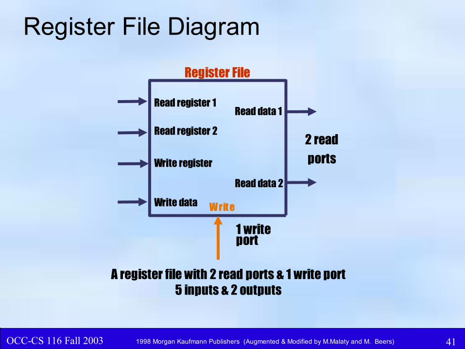
Register File Diagram
Read register 1
W rit e
Read register 2
Write register
Write data
Read data 1
Read data 2
Register File
2 readports
1 write port
A register file with 2 read ports & 1 write port5 inputs & 2 outputs
OCC - CS/CIS CS116-Ch00-Orientation 421998 Morgan Kaufmann Publishers ( Augmented & Modif ied by M.Malaty) 42OCC-CS 116 Fall 2003 1998 Morgan Kaufmann Publishers (Augmented & Modified by M.Malaty and M. Beers)
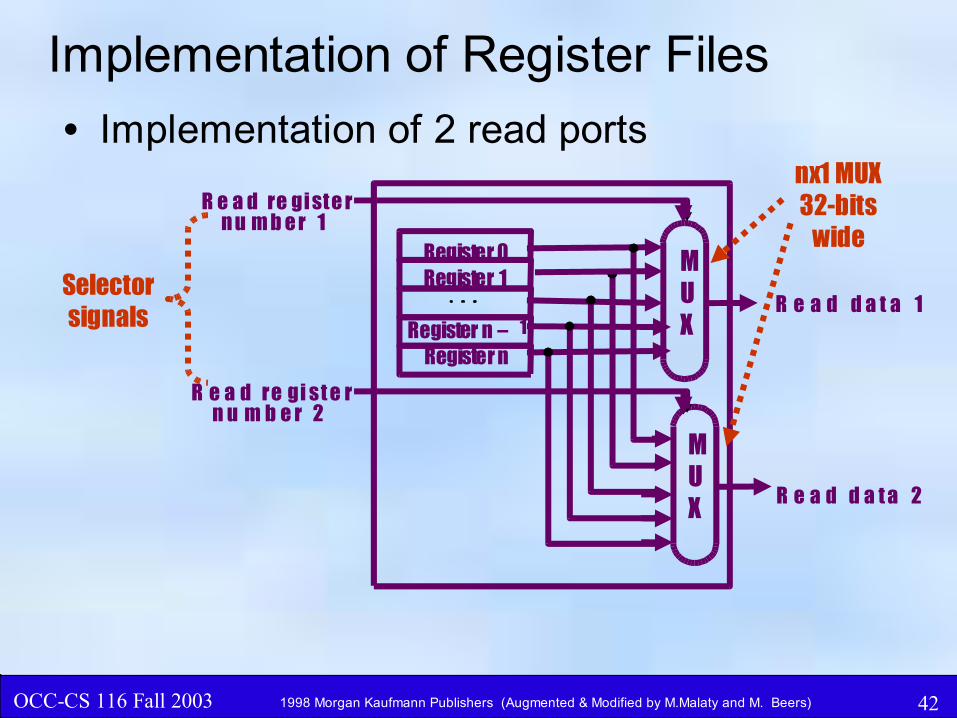
Implementation of Register Files
• Implementation of 2 read ports
1
Register 0Register 1
Register n – Register n
R e a d d a t a 1
R e a d d a t a 2
R e a d re gi st e rn u m b e r 1
R e a d re gi st e rn u m b e r 2
Selector signals
nx1 MUX 32-bits
wideMUX
MUX
OCC - CS/CIS CS116-Ch00-Orientation 431998 Morgan Kaufmann Publishers ( Augmented & Modif ied by M.Malaty) 43OCC-CS 116 Fall 2003 1998 Morgan Kaufmann Publishers (Augmented & Modified by M.Malaty and M. Beers)
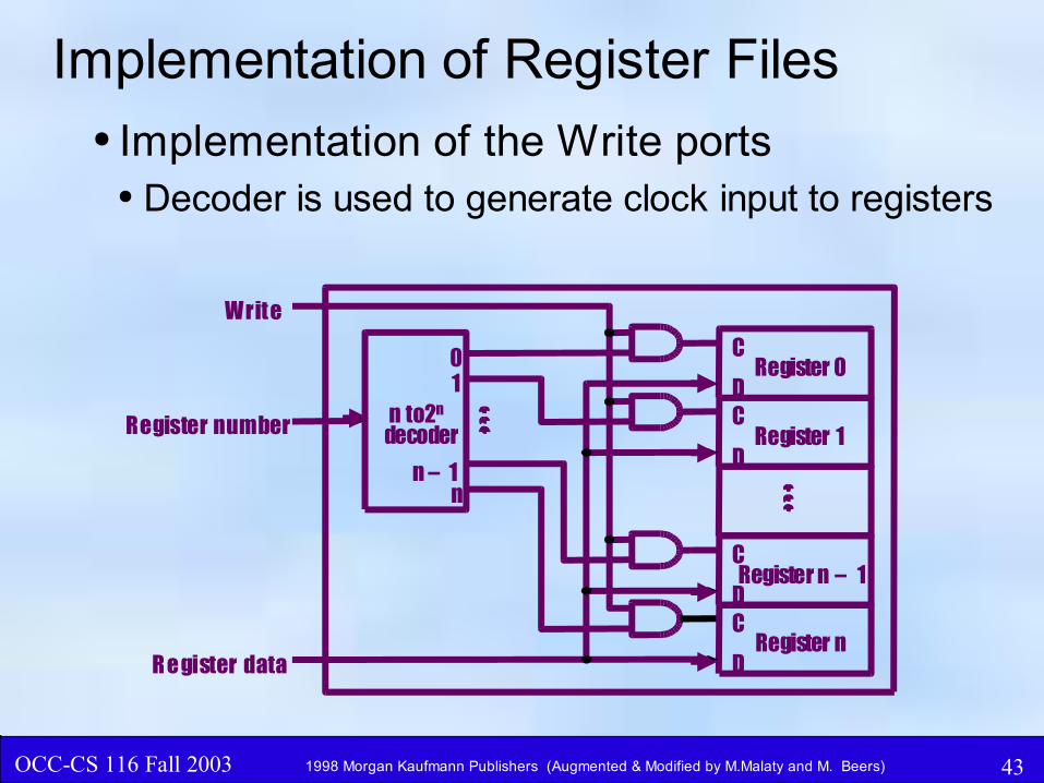
Implementation of Register Files● Implementation of the Write ports
● Decoder is used to generate clock input to registers
Register 0
Register 1
Register n – 1
Register n
Register number
Write
R e gister data
n – 1
n to2n
decoder
01
n
C
CD
D
C
CD
D
OCC - CS/CIS CS116-Ch00-Orientation 441998 Morgan Kaufmann Publishers ( Augmented & Modif ied by M.Malaty) 44OCC-CS 116 Fall 2003 1998 Morgan Kaufmann Publishers (Augmented & Modified by M.Malaty and M. Beers)
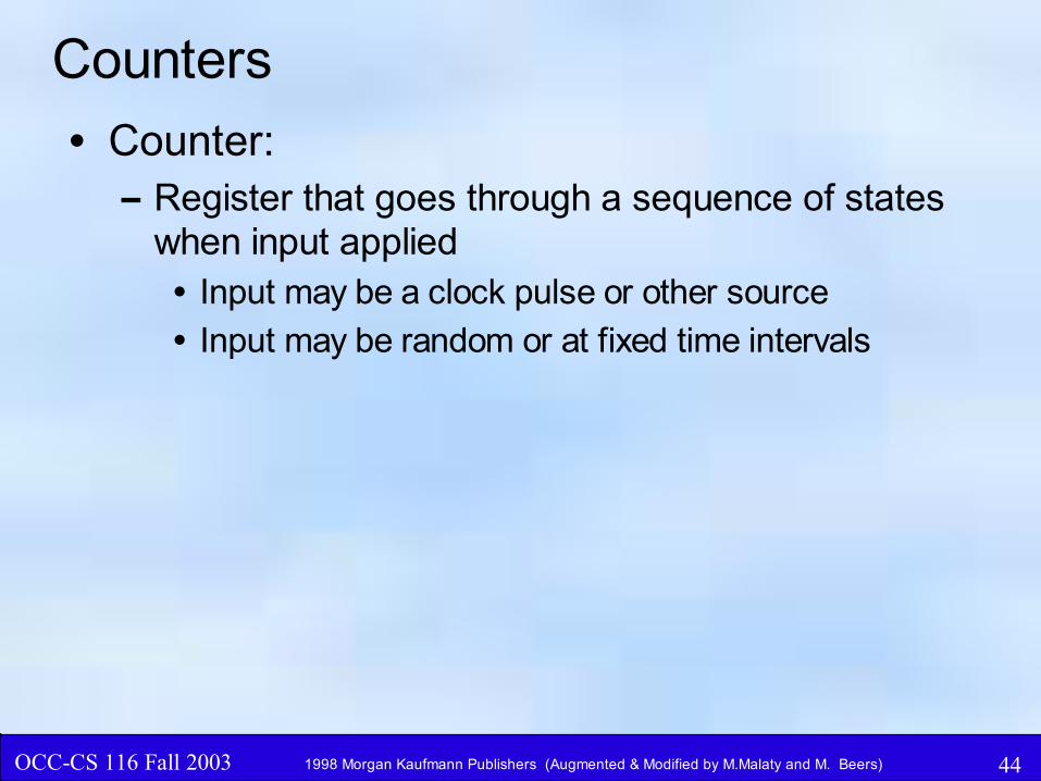
Counters
• Counter:– Register that goes through a sequence of states
when input applied• Input may be a clock pulse or other source
• Input may be random or at fixed time intervals

OCC - CS/CIS CS116-Ch00-Orientation 451998 Morgan Kaufmann Publishers ( Augmented & Modif ied by M.Malaty) 45OCC-CS 116 Fall 2003 1998 Morgan Kaufmann Publishers (Augmented & Modified by M.Malaty and M. Beers)
Binary Counters
• Clock input
• A number of count outputs which give the number of clock cycles. – The output may change either on rising or falling
clock edges.
• May also have a reset input
• The counter may be either a synchronous counter or a ripple counter

OCC - CS/CIS CS116-Ch00-Orientation 461998 Morgan Kaufmann Publishers ( Augmented & Modif ied by M.Malaty) 46OCC-CS 116 Fall 2003 1998 Morgan Kaufmann Publishers (Augmented & Modified by M.Malaty and M. Beers)
Other Counters
• n-bit binary counter:– Counts from 0 to 2n-1
– Needs n-FFs
• Synchronous counter:– All FFs have common clock
– State change determined from the present state
• Ripple counter:– The output of one FF is used
to trigger another FF
Q0
Q1
Q2
3-Bit Ripple-Counter
CQJ
K
Clock
CQJ
K
CQJ
K
Logic 1
OCC - CS/CIS CS116-Ch00-Orientation 471998 Morgan Kaufmann Publishers ( Augmented & Modif ied by M.Malaty) 47OCC-CS 116 Fall 2003 1998 Morgan Kaufmann Publishers (Augmented & Modified by M.Malaty and M. Beers)
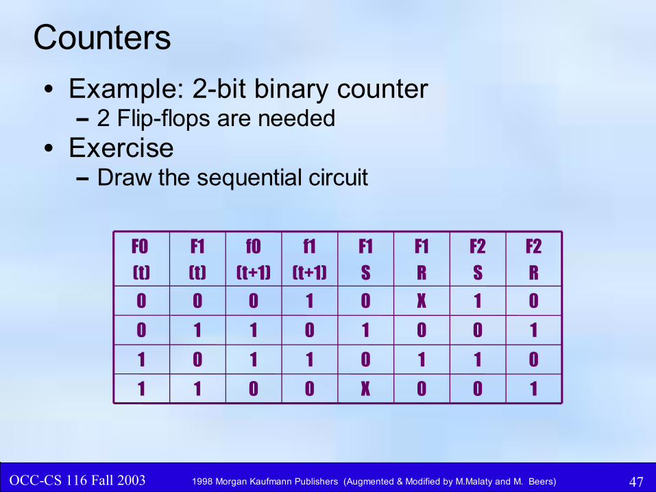
Counters
• Example: 2-bit binary counter– 2 Flip-flops are needed
• Exercise– Draw the sequential circuit
100X0011
01101101
10010110
01X01000
F2R
F2S
F1R
F1S
f1(t+1)
f0(t+1)
F1(t)
F0 (t)

OCC - CS/CIS CS116-Ch00-Orientation 481998 Morgan Kaufmann Publishers ( Augmented & Modif ied by M.Malaty) 48OCC-CS 116 Fall 2003 1998 Morgan Kaufmann Publishers (Augmented & Modified by M.Malaty and M. Beers)
Programmable Logic devices (PLD)
• Programmable Logic:– A logic element whose function is not restricted to
a particular function.
– May be programmed at different points of the life cycle
• PLD Compiler:– A software tool that converts functional description
into a set of interconnections that can be programmed into the PLD.
OCC - CS/CIS CS116-Ch00-Orientation 491998 Morgan Kaufmann Publishers ( Augmented & Modif ied by M.Malaty) 49OCC-CS 116 Fall 2003 1998 Morgan Kaufmann Publishers (Augmented & Modified by M.Malaty and M. Beers)
PLD Details
• A large-scale integration (LSI) chip – Contains regular circuit structure
– Is programmed by the purchaser
• Implementation– A programmable AND array followed by a fixed
fan-in OR gates that are followed by flip-flops.
• Product lines can be any input combination and flip-flops can be fed back to input.
• Programmable element can be fuse or a transistor.
OCC - CS/CIS CS116-Ch00-Orientation 501998 Morgan Kaufmann Publishers ( Augmented & Modif ied by M.Malaty) 50OCC-CS 116 Fall 2003 1998 Morgan Kaufmann Publishers (Augmented & Modified by M.Malaty and M. Beers)
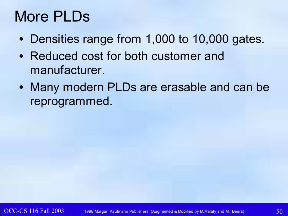
More PLDs
• Densities range from 1,000 to 10,000 gates.
• Reduced cost for both customer and manufacturer.
• Many modern PLDs are erasable and can be reprogrammed.

OCC - CS/CIS CS116-Ch00-Orientation 511998 Morgan Kaufmann Publishers ( Augmented & Modif ied by M.Malaty) 51OCC-CS 116 Fall 2003 1998 Morgan Kaufmann Publishers (Augmented & Modified by M.Malaty and M. Beers)
Basic PLD Block Diagram
i/pbuffer
Product(AND)
Matrix
Sum(OR)
Matrix
o/pbuffer
Bp
B0
n o/p lines
A’m
Am
A’0
A0
,
,
,
,
,
,
,
,
,
,
,
,m i/plines
2 m i/plines &
complements

OCC - CS/CIS CS116-Ch00-Orientation 521998 Morgan Kaufmann Publishers ( Augmented & Modif ied by M.Malaty) 52OCC-CS 116 Fall 2003 1998 Morgan Kaufmann Publishers (Augmented & Modified by M.Malaty and M. Beers)
Programmable Logic Array (PLA)
• A combinational circuit, – 2-level, AND-OR device programmed
– Can realize any sum-of-product logic expressions
• Has both programmable AND and OR planes.– Programmed by establishing the connections that
are actually needed.

OCC - CS/CIS CS116-Ch00-Orientation 531998 Morgan Kaufmann Publishers ( Augmented & Modif ied by M.Malaty) 53OCC-CS 116 Fall 2003 1998 Morgan Kaufmann Publishers (Augmented & Modified by M.Malaty and M. Beers)
Programmable Logic Array (PLA)● A set of inputs and input complements
● Two stages of logic.● First: Array of AND gates (AND-plane)
● Forms a set of product terms.● Array of OR gates (OR-plane),
● May be a logical sum of any number of the product terms.
● Can directly implement truth table ● The number of OR gates correspond to the
number of truth table entries for which the output is true.
A N D gates
O R gates Outputs
Inputs
Product terms
OCC - CS/CIS CS116-Ch00-Orientation 541998 Morgan Kaufmann Publishers ( Augmented & Modif ied by M.Malaty) 54OCC-CS 116 Fall 2003 1998 Morgan Kaufmann Publishers (Augmented & Modified by M.Malaty and M. Beers)
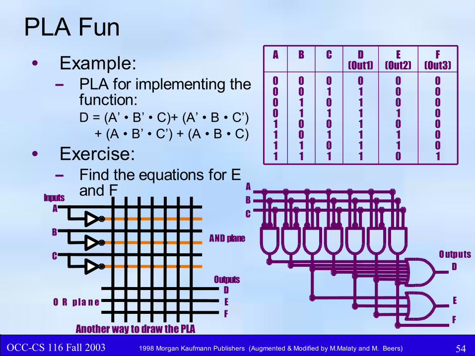
PLA Fun• Example:
– PLA for implementing the function:D = (A’ • B’ • C)+ (A’ • B • C’) + (A • B’ • C’) + (A • B • C)
• Exercise:– Find the equations for E
and FA
B
C
Inputs
DEF
Outputs
AND plane
O R p la n e
Another way to draw the PLA
DO utputs
E
F
ABC
00000001
00010110
01111111
01010101
00110011
00001111
F (Out3)
E (Out2)
D (Out1)
CBA

OCC - CS/CIS CS116-Ch00-Orientation 551998 Morgan Kaufmann Publishers ( Augmented & Modif ied by M.Malaty) 55OCC-CS 116 Fall 2003 1998 Morgan Kaufmann Publishers (Augmented & Modified by M.Malaty and M. Beers)
Read-Only Memories (ROMs)
• Definitions: – Nonvolatile memory that can only be read
– A combinational circuit • n-address inputs
• b-data outputs
• Encodes logic functions directly from truth tables.
– Manufactured with fixed contents
– Internal structure works with diodes or transistors.• The presence or absence of a diode or a transistor
distinguishes between 0 and 1.
– Modern ROMs are fabricated as a single IC chip.
OCC - CS/CIS CS116-Ch00-Orientation 561998 Morgan Kaufmann Publishers ( Augmented & Modif ied by M.Malaty) 56OCC-CS 116 Fall 2003 1998 Morgan Kaufmann Publishers (Augmented & Modified by M.Malaty and M. Beers)
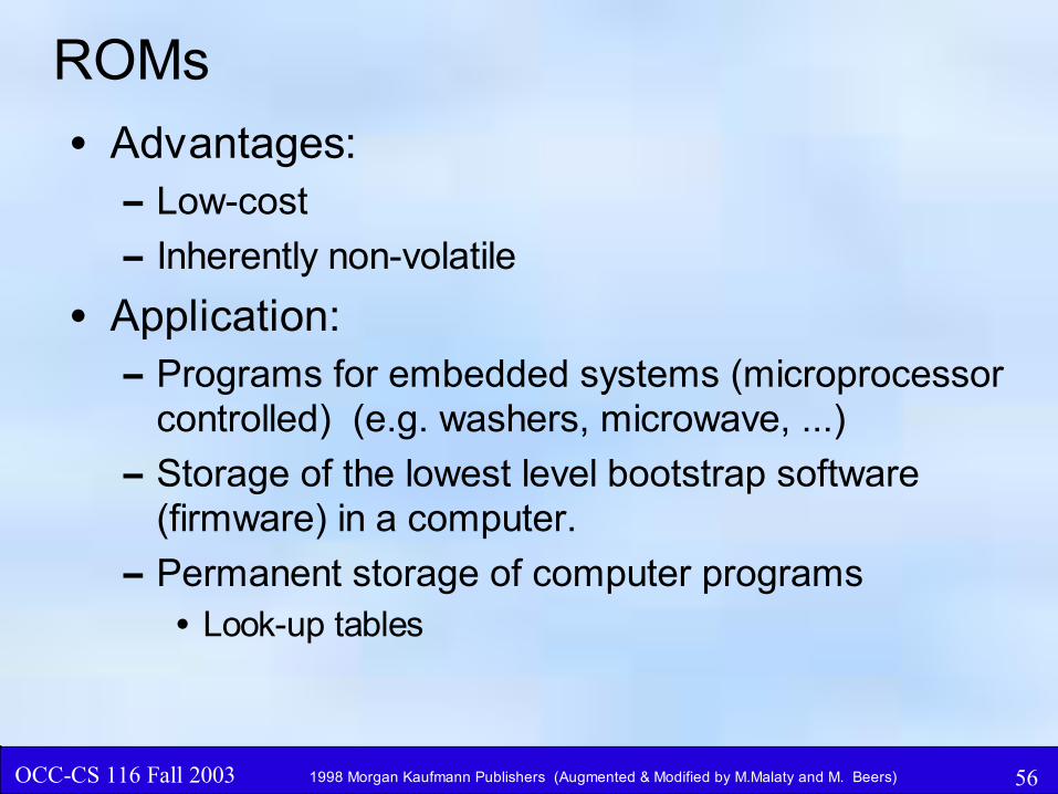
ROMs
• Advantages:– Low-cost
– Inherently non-volatile
• Application:– Programs for embedded systems (microprocessor
controlled) (e.g. washers, microwave, ...)
– Storage of the lowest level bootstrap software (firmware) in a computer.
– Permanent storage of computer programs• Look-up tables

OCC - CS/CIS CS116-Ch00-Orientation 571998 Morgan Kaufmann Publishers ( Augmented & Modif ied by M.Malaty) 57OCC-CS 116 Fall 2003 1998 Morgan Kaufmann Publishers (Augmented & Modified by M.Malaty and M. Beers)
ROMs
• Characteristics:– Input (height):
• 2n addressable entries (Address lines) & n-input lines.
– Output (Width):• Number of bits (d) in each addressable entry.
– Total number of bits = Height x Width.

OCC - CS/CIS CS116-Ch00-Orientation 581998 Morgan Kaufmann Publishers ( Augmented & Modif ied by M.Malaty) 58OCC-CS 116 Fall 2003 1998 Morgan Kaufmann Publishers (Augmented & Modified by M.Malaty and M. Beers)
ROM Variations
• Programmable ROMs (PROMs):– Can be programmed electronically, when the
designer knows their contents.
• Erasable PROMs (EPROMs):– Requires slow erasure process using ultraviolet
light.
– Special devices are needed for reprogramming
• Electrically Erasable PROM(EEPROM):– Stored bits may be electrically erased.
OCC - CS/CIS CS116-Ch00-Orientation 591998 Morgan Kaufmann Publishers ( Augmented & Modif ied by M.Malaty) 59OCC-CS 116 Fall 2003 1998 Morgan Kaufmann Publishers (Augmented & Modified by M.Malaty and M. Beers)
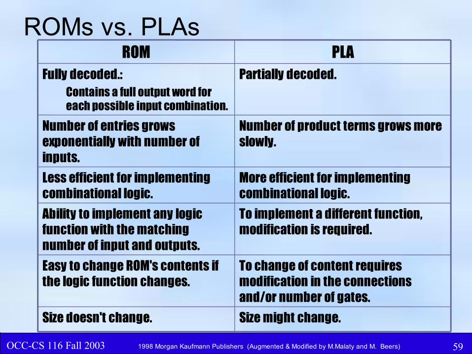
ROMs vs. PLAs
Size might change.Size doesn't change.
To change of content requires modification in the connections and/or number of gates.
Easy to change ROM's contents if the logic function changes.
To implement a different function, modification is required.
Ability to implement any logic function with the matching number of input and outputs.
More efficient for implementing combinational logic.
Less efficient for implementing combinational logic.
Number of product terms grows more slowly.
Number of entries grows exponentially with number of inputs.
Partially decoded. Fully decoded.:Contains a full output word for each possible input combination.
PLAROM
OCC - CS/CIS CS116-Ch00-Orientation 601998 Morgan Kaufmann Publishers ( Augmented & Modif ied by M.Malaty) 60OCC-CS 116 Fall 2003 1998 Morgan Kaufmann Publishers (Augmented & Modified by M.Malaty and M. Beers)
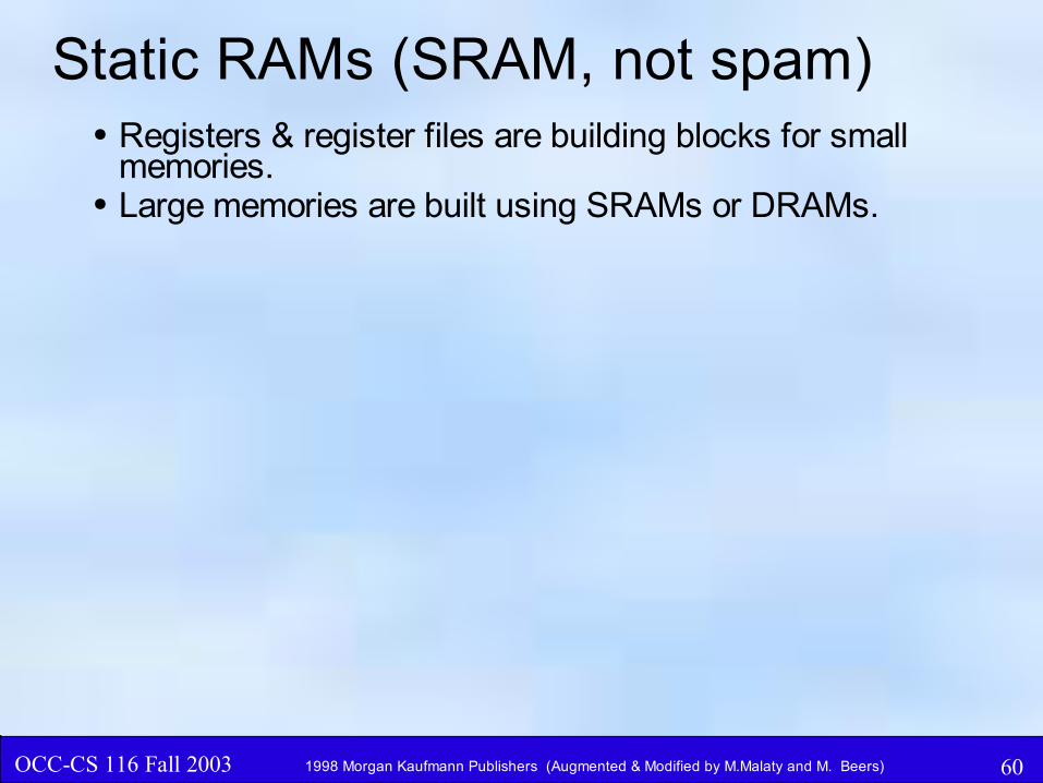
Static RAMs (SRAM, not spam)● Registers & register files are building blocks for small
memories.● Large memories are built using SRAMs or DRAMs.

OCC - CS/CIS CS116-Ch00-Orientation 611998 Morgan Kaufmann Publishers ( Augmented & Modif ied by M.Malaty) 61OCC-CS 116 Fall 2003 1998 Morgan Kaufmann Publishers (Augmented & Modified by M.Malaty and M. Beers)
SRAM• SRAM is:
– Each bit of storage is a bistable flip-flop
– Will retain a value as long as power is supplied
– Refresh regularly, unlike dynamic random access memory (DRAM).
– Will lose its contents when the power is turned off, unlike ROM
– IC-chips memory arrays with read/write port.
– The value kept in a cell is kept on a pair of inverting gates.
– As long as power is applied, the value is kept indefinitely.

OCC - CS/CIS CS116-Ch00-Orientation 621998 Morgan Kaufmann Publishers ( Augmented & Modif ied by M.Malaty) 62OCC-CS 116 Fall 2003 1998 Morgan Kaufmann Publishers (Augmented & Modified by M.Malaty and M. Beers)
Static RAMs (SRAM)• Type of SRAM is defined by:
– Width and height:
– Number of addressable locations
– Width of each addressable location
• SRAMs have fixed access time (5-25ns).
• Address line depends in the first number– To initiate read/write access, the Chip select signal
must be active.
– The Output enable signal allows the output data to be accessed.

OCC - CS/CIS CS116-Ch00-Orientation 631998 Morgan Kaufmann Publishers ( Augmented & Modif ied by M.Malaty) 63OCC-CS 116 Fall 2003 1998 Morgan Kaufmann Publishers (Augmented & Modified by M.Malaty and M. Beers)
SRAM Example• Example:
256k x 1 SRAM 256k (=218) entries, each 1-bit wide needs 18 address1 data input1 data output lines 32k x 8 SRAM 32k (=215 )entries, each 8 bits wide Needs 15 address8 data output 8 data input lines are needed
D o u t[ 7 – 0 ]
S R A M
3 2 K ´ 8
8
1 5
8
A d d r e s s
C h i p s e le c tO u t p u t e n a b l e
W r it e e n a b l e
D i n [ 7 – 0 ]
OCC - CS/CIS CS116-Ch00-Orientation 641998 Morgan Kaufmann Publishers ( Augmented & Modif ied by M.Malaty) 64OCC-CS 116 Fall 2003 1998 Morgan Kaufmann Publishers (Augmented & Modified by M.Malaty and M. Beers)
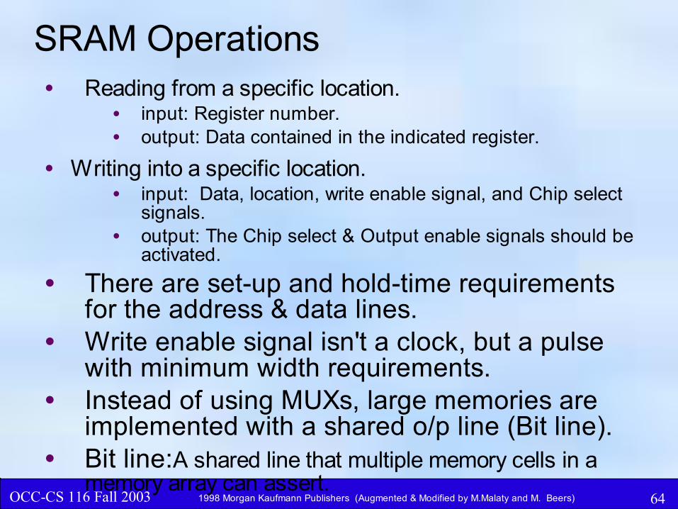
SRAM Operations• Reading from a specific location.
• input: Register number.• output: Data contained in the indicated register.
• Writing into a specific location.• input: Data, location, write enable signal, and Chip select
signals.• output: The Chip select & Output enable signals should be
activated.
• There are set-up and hold-time requirements for the address & data lines.
• Write enable signal isn't a clock, but a pulse with minimum width requirements.
• Instead of using MUXs, large memories are implemented with a shared o/p line (Bit line).
• Bit line:A shared line that multiple memory cells in a memory array can assert.

OCC - CS/CIS CS116-Ch00-Orientation 651998 Morgan Kaufmann Publishers ( Augmented & Modif ied by M.Malaty) 65OCC-CS 116 Fall 2003 1998 Morgan Kaufmann Publishers (Augmented & Modified by M.Malaty and M. Beers)
Basic Structure of a 4x2 SRAM
Dlatch Q
DCEnable
Dlatch Q
DCEnable
Dlatch Q
DCEnable
Dlatch Q
DCEnable
Dlatch Q
DCEnable
Dlatch Q
DCEnable
Dlatch Q
DCEnable
Dlatch Q
DCEnable
2-to-4decoder
Write enable
Address
Din[0]Din[1]
Dout[1] Dout[0]
0
1
2
3
OCC - CS/CIS CS116-Ch00-Orientation 661998 Morgan Kaufmann Publishers ( Augmented & Modif ied by M.Malaty) 66OCC-CS 116 Fall 2003 1998 Morgan Kaufmann Publishers (Augmented & Modified by M.Malaty and M. Beers)
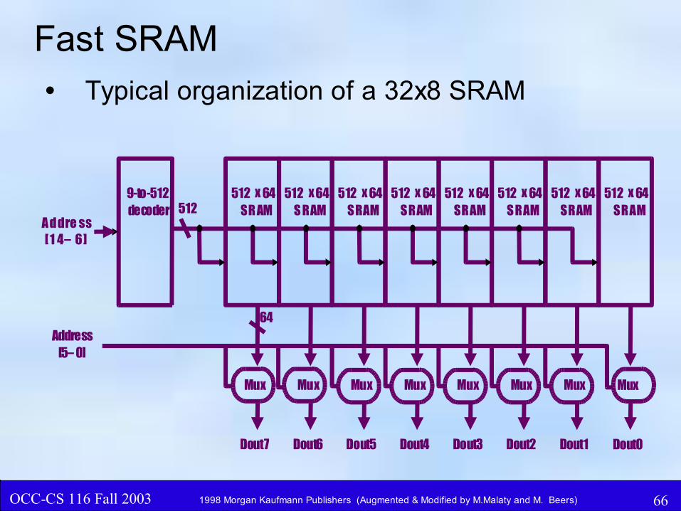
Fast SRAM• Typical organization of a 32x8 SRAM
512 x 64SR AM
512 x 64S RAM
512 x 64SRAM
512 x 64SRAM
512 x 64SRAM
512 x 64S RAM
512 x 64SRAM
512 x 64SRAM
9-to-512decoder
A d dre ss[ 1 4– 6]
512
Mux
Dout7
Mux
Dout6
Mux
Dout5
Mux
Dout4
Mux
Dout3
Mux
Dout2
Mux
Dout1
Mux
Dout0
64Address
[5– 0]

OCC - CS/CIS CS116-Ch00-Orientation 671998 Morgan Kaufmann Publishers ( Augmented & Modif ied by M.Malaty) 67OCC-CS 116 Fall 2003 1998 Morgan Kaufmann Publishers (Augmented & Modified by M.Malaty and M. Beers)
Dynamic RAMs (DRAMs)
• The value kept in a cell is stored as a charge in a capacitor.– A single transistor is used to access the stored
charge.
• The value can't be kept indefinitely– Must be periodically refreshed.
– The charge can be kept for few milliseconds.
• Refreshing the cell– Read the data and then write it back.
• Two-level decoding structure is used, that allows an entire row to be refreshed.

OCC - CS/CIS CS116-Ch00-Orientation 681998 Morgan Kaufmann Publishers ( Augmented & Modif ied by M.Malaty) 68OCC-CS 116 Fall 2003 1998 Morgan Kaufmann Publishers (Augmented & Modified by M.Malaty and M. Beers)
DRAM
• To save pins & reduce cost, the same address lines are used for both rows & column addresses.– The access is slower than SRAMs. Typical DRAM
access times range from 60 - 110 ns.
– Row Access Strobe (RAS): used to signal row addressing.
– Column Access Strobe (CAS): Used to signal column addressing.

OCC - CS/CIS CS116-Ch00-Orientation 691998 Morgan Kaufmann Publishers ( Augmented & Modif ied by M.Malaty) 69OCC-CS 116 Fall 2003 1998 Morgan Kaufmann Publishers (Augmented & Modified by M.Malaty and M. Beers)
More DRAM
• A single transistor DRAM
• A 4M x 1 DRAM with a 2048 x 2048 array
Word line
Pass transistor
Capacitor
Bit line
Word line
Pass transistor
Capacitor
Bit line
A ddre ss[ 1 0– 0]
R owdeco de r
1 1 -to -20 4820 48 x 204 8
arra y
C olu m n latche s
M u x
D o ut

OCC - CS/CIS CS116-Ch00-Orientation 701998 Morgan Kaufmann Publishers ( Augmented & Modif ied by M.Malaty) 70OCC-CS 116 Fall 2003 1998 Morgan Kaufmann Publishers (Augmented & Modified by M.Malaty and M. Beers)
Error Detection & Correction
• Most computer systems use some sort of error-checking code to detect possible corruption of data.
• A collection of methods to detect errors in transmitted or stored data and to correct them.
• Involves some form of encoding
OCC - CS/CIS CS116-Ch00-Orientation 711998 Morgan Kaufmann Publishers ( Augmented & Modif ied by M.Malaty) 71OCC-CS 116 Fall 2003 1998 Morgan Kaufmann Publishers (Augmented & Modified by M.Malaty and M. Beers)
Error Checking Method
• Single parity:– The simplest form of error detection is a single
added parity bit or a cyclic redundancy check.
– Parity code:• The number of 1's in a word is counted.
– Odd parity:• If the number of 1's is odd.
– Even parity:• If the number of 1's is even.
– Parity can only detect, but not correct errors.
– Only odd number of errors can be detected.
OCC - CS/CIS CS116-Ch00-Orientation 721998 Morgan Kaufmann Publishers ( Augmented & Modif ied by M.Malaty) 72OCC-CS 116 Fall 2003 1998 Morgan Kaufmann Publishers (Augmented & Modified by M.Malaty and M. Beers)
Error Detection & Correction
• Multiple parity:– Detect that an error has occurred – Which bits have been inverted, – The more extra bits are added, the greater the
chance that multiple errors will be detectable and correctable.
• Several codes can perform – Single Error Correction, Double Error Detection
(SECDEC).
– One of the most common is the Hamming code. • Other error-correcting codes exist and allow
detection as well as correction of errors. More bits are used to encode the data.
OCC - CS/CIS CS116-Ch00-Orientation 731998 Morgan Kaufmann Publishers ( Augmented & Modif ied by M.Malaty) 73OCC-CS 116 Fall 2003 1998 Morgan Kaufmann Publishers (Augmented & Modified by M.Malaty and M. Beers)
Buses
• A set of electrical connections (wires) through which signals (and power) can pass. – May be either synchronous or asynchronous
• In a computer bus signals usually synchronous,– Controlled by the system clock.
OCC - CS/CIS CS116-Ch00-Orientation 741998 Morgan Kaufmann Publishers ( Augmented & Modif ied by M.Malaty) 74OCC-CS 116 Fall 2003 1998 Morgan Kaufmann Publishers (Augmented & Modified by M.Malaty and M. Beers)
Different Busses
• Data bus :– 8, 16, 32, 64, 80 (or more) wires for transmission
– Bi-directional
– Parallel
• Address bus :– Governs the amount of memory that a computer
can address.
– Unidirectional, only the processor can 'address' memory
– Parallel

OCC - CS/CIS CS116-Ch00-Orientation 751998 Morgan Kaufmann Publishers ( Augmented & Modif ied by M.Malaty) 75OCC-CS 116 Fall 2003 1998 Morgan Kaufmann Publishers (Augmented & Modified by M.Malaty and M. Beers)
• Control Bus :– This includes all the different wires to carry power,
earth, clock signals, interrupts, controls for other buses, connections to other processors and chips, logic signals, any other electrical connections at 5V or below.
– Consists (mostly) of individual wires.
– Serial

OCC - CS/CIS CS116-Ch00-Orientation 761998 Morgan Kaufmann Publishers ( Augmented & Modif ied by M.Malaty) 76OCC-CS 116 Fall 2003 1998 Morgan Kaufmann Publishers (Augmented & Modified by M.Malaty and M. Beers)
Bus Picture
I/O
DataAddress
Control
CPU Memory

OCC - CS/CIS CS116-Ch00-Orientation 771998 Morgan Kaufmann Publishers ( Augmented & Modif ied by M.Malaty) 77OCC-CS 116 Fall 2003 1998 Morgan Kaufmann Publishers (Augmented & Modified by M.Malaty and M. Beers)
Bus business
• Bus notation:– Usually has its own name
– Drawn with either a double arrow or a thick line.
• Assumption– A bus with no label is assumed to be32-bits wide
– If not 32-bits it will be explicitly indicated on the graph.