c8051f530a development kit user's guide
TRANSCRIPT

Rev. 0.4 11/14 Copyright © 2014 by Silicon Laboratories C8051F53x/52x
C8051F53x/52x
C8051F530A DEVELOPMENT KIT USER’S GUIDE
1. Relevant DevicesThe C8051F530 Development Kit is intended as a development platform for microcontrollers in the C8051F53x/52x MCU family. Code developed on the C8051F530 can be easily ported to the other members of this MCUfamily.
2. Kit ContentsThe C8051F530 Development Kit contains the following items:
C8051F530A Target Board
C8051Fxxx Development Kit Quick-Start Guide
AC to DC Power Adapter
USB Debug Adapter (USB to Debug Interface)
USB Cable
The development kit target board contains two C8051F530 microcontrollers that can communicate through an LINnetwork. One of the C8051F530 (U2) can also be connected to a CP2102 USB to UART bridge and directlyconnected to two analog signals and a Voltage Reference Signal Input.
3. Hardware Setup Using a USB Debug AdapterThe target board is connected to a PC running the Silicon Laboratories IDE via the USB Debug Adapter as shownin Figure 1.
1. Connect the USB Debug Adapter to one of the DEBUG connectors on the target board (HDR1 or HDR2) with the 10-pin ribbon cable. The recommended connection is to the HDR2 (connected to U2) as this microcontroller can be connected to the CP2102 USB to UART bridge.
2. Verify that shorting blocks are installed on J13 and J14 to supply power to the target devices.
3. Connect one end of the USB cable to the USB connector on the USB Debug Adapter.
4. Connect the other end of the USB cable to a USB Port on the PC.
5. Connect the ac/dc power adapter to power jack P5 on the target board.
Figure 1. Hardware Setup using a USB Debug Adapter
P5P1
P1.
4_A
P1.
4_B
U3
U1
U2
SILI
CO
N
LABO
RAT
OR
IES
C80
51F
530A
TB
PW
R
D1
D2
T1
T2
J4
P1.7_BJ3
P1.6_B
J5
P0.0_B
DE
BU
G_
B
HDR1Reset_B
DE
BU
G_A
HDR2Reset_A
HD
R3
“B”
Sid
e
“A”
Sid
e
J13
J14
J8
J6
HDR4
PC
USB Cable
USB Debug Adapter
AC/DCAdapter
Target Board
Silicon Laboratories
US
B D
EB
UG
AD
AP
TE
R
Ru
n
Sto
pP
ow
er

C8051F53x/52x
2 Rev. 0.4
Notes:1. Use the Reset button in the IDE to reset the target when connected using a USB Debug Adapter.2. Remove power from the target board and the USB Debug Adapter before connecting or disconnecting the
ribbon cable from the target board. Connecting or disconnecting the cable when the devices have power can damage the device and/or the USB Debug Adapter.
4. Software SetupSimplicity Studio greatly reduces development time and complexity with Silicon Labs EFM32 and 8051 MCUproducts by providing a high-powered IDE, tools for hardware configuration, and links to helpful resources, all inone place.
Once Simplicity Studio is installed, the application itself can be used to install additional software anddocumentation components to aid in the development and evaluation process.
Figure 2. Simplicity Studio
The following Simplicity Studio components are required for the C8051F530 Development Kit:
8051 Products Part Support
Simplicity Developer Platform
Download and install Simplicity Studio from www.silabs.com/8bit-software or www.silabs.com/simplicity-studio.Once installed, run Simplicity Studio by selecting StartSilicon LabsSimplicity StudioSimplicity Studiofrom the start menu or clicking the Simplicity Studio shortcut on the desktop. Follow the instructions to install thesoftware and click Simplicity IDE to launch the IDE.
The first time the project creation wizard runs, the Setup Environment wizard will guide the user through theprocess of configuring the build tools and SDK selection.

C8051F53x/52x
Rev. 0.4 3
In the Part Selection step of the wizard, select from the list of installed parts only the parts to be used duringdevelopment. Choosing parts and families in this step affects the displayed or filtered parts in the later deviceselection menus. Choose the C8051F53x/52x family by checking the C8051F53x/52x check box. Modify the partselection at any time by accessing the Part Management dialog from the WindowPreferencesSimplicityStudioPart Management menu item.
Simplicity Studio can detect if certain toolchains are not activated. If the Licensing Helper is displayed aftercompleting the Setup Environment wizard, follow the instructions to activate the toolchain.
4.1. Running BlinkyEach project has its own source files, target configuration, SDK configuration, and build configurations such as theDebug and Release build configurations. The IDE can be used to manage multiple projects in a collection called aworkspace. Workspace settings are applied globally to all projects within the workspace. This can include settings,such as key bindings, window preferences, and code style and formatting options. Project actions, such as buildand debug, are context-sensitive. For example, the user must select a project in the Project Explorer view in orderto build that project.
To create a project based on the Blinky example, perform the following steps:
1. Click the Software Examples tile from the Simplicity Studio home screen.
2. In the Kit drop-down, select C8051F530A Development Kit; in the Part drop-down, select C8051F530, and in the SDK drop-down, select the desired SDK. Click Next.
3. Select Example, and click Next.
4. Under C8051F530A Development Kit, select F52x-53x Blinky; click Next, and click Finish.
5. Click on the project in the Project Explorer, and click Build (the hammer icon in the top bar). Alternatively, go to ProjectBuild Project.
6. Click Debug to download the project to the hardware and start a debug session.
7. Press the Resume button to start the code running. The LED should blink.
8. Press the Suspend button to stop the code.
9. Press the Reset the device button to reset the target MCU.
10. Press the Disconnect button to return to the development perspective.
4.2. Simplicity Studio HelpSimplicity Studio includes detailed help information and device documentation within the tool. The help containsdescriptions for each dialog window. To view the documentation for a dialog, click the question mark icon in thewindow:
This will open a pane specific to the dialog with additional details.
The documentation within the tool can also be viewed by going to HelpHelp Contents or HelpSearch.

C8051F53x/52x
4 Rev. 0.4
4.3. CP210x USB to UART VCP Driver InstallationThe Target Board includes a Silicon Labs CP210x USB-to-UART Bridge Controller. Device drivers for the CP210xneed to be installed before the PC software can communicate with the MCU through the UART interface.
1. After opening Simplicity Studio for the first time, a dialog will prompt to install the CP210x drivers. Click Yes. The drivers can also be installed at any time by going to HelpInstall DriversCP210x VCP USB Drivers.
2. Accept the license agreement and follow the steps to install the driver on the system. The installer will let you know when your system is up to date. The driver files included in this installation have been certified by Microsoft.
3. To complete the installation process, connect the included USB cable between the host computer and the USB connector (P4) on the Target Board. Windows will automatically finish the driver installation. Information windows will pop up from the taskbar to show the installation progress.
4. If necessary, the driver files can be uninstalled by selecting Windows Driver Package—Silicon Laboratories... option in the Programs and Features window.
4.4. Configuration Wizard 2The Configuration Wizard 2 is a code generation tool for all of the Silicon Laboratories devices. Code is generatedthrough the use of dialog boxes for each of the device's peripherals.
Figure 3. Configuration Wizard 2 Utility
The Configuration Wizard 2 utility helps accelerate development by automatically generating initialization sourcecode to configure and enable the on-chip resources needed by most design projects. In just a few steps, the wizardcreates complete startup code for a specific Silicon Laboratories MCU. The program is configurable to provide theoutput in C or assembly language. For more information, refer to the Configuration Wizard documentation.Documentation and software is available on the kit CD and from the downloads web page: www.silabs.com/mcudownloads.

C8051F53x/52x
Rev. 0.4 5
5. Target Board
The C8051F52xA-53xA Development Kit includes a target board with two C8051F530A devices preinstalled forevaluation and preliminary software development. Numerous input/output (I/O) connections are provided tofacilitate prototyping using the target board. Refer to Figure 4 for the locations of the various I/O connectors.
Table 1. Target Board Part Summary
Part Description
P5 Power connector (Accepts input from 7 to 15 VDC unregulated power adapter.)
PWR Red Power-on LED (D3)
TB1 LIN connector
U5 5 V Voltage Regulator
A Side
J2 28-pin Expansion I/O connector for U2
HDR2 Debug connector for Debug Adapter Interface
P1.3_A Green LED (D2)
Reset_A Reset button
P1.4_A Push button
R32 Potentiometer for P1.2_A
J6, J8 Connects R32 (potentiometer) to U2 and +5 V
J13 Connects power to U2
J11, J12 Connects external crystal to U2 pins P0.7_A and P1.0_A
J3 Connects analog channel 1 to U2 P1.6_A
J4 Connects analog channel 2 to U2 P1.7_A
J5 Connects VREFIN to U2 P0.0_A
TB2 Analog input connector
HDR4 Connector block for serial port connection, Green LED, and push-button
U3 Silicon Laboratories CP2102 USB-to-UART Bridge
P1 USB connector to serial interface (CP2102)
USB ACTIVE Red USB Active LED (D4) (CP2102)
T2 LIN transceiver
U2 C8051F530A “A” Side

C8051F53x/52x
6 Rev. 0.4
5.1. Target Board Shorting Blocks: Factory DefaultsThe C8051F530A target board comes from the factory with preinstalled shorting blocks on many headers. Figure 4shows the positions of the factory default shorting blocks.
Figure 4. C8051F530A Target Board
B Side
J1 26-pin Expansion I/O connector for U1
HDR1 Debug connector for Debug Adapter Interface
P1.3_B Green LED (D1)
Reset_B Reset button
P1.4_B Push button
J14 Connects power to U1
J9, J10 Connects external crystal to U1 pins P0.7_B and P1.0_B
HDR3 Green LED and push-button connector block
T1 LIN transceiver
U1 C8051F530A “B” Side
Table 1. Target Board Part Summary
Part Description
P5
P1
P1.4_A
P1.4_B
U3
U1
U2
SILICON LABORATORIES
C8051F530A TB
T1
T2
J4
P1.
7_A
J3
P1.
6_A
J5
P0.
0_A
+1
2VL
ING
ND
GNDCH2 CH1 VRefin
DEBUG_B
HD
R1
Re
set_
B
DEBUG_A
HD
R2
Res
et_
A
HDR3
“B” Side
“A” Side
J13
J14
J8
J6
HD
R4
J12
J11
J10
J9
PWR
USB ACTIVE
P1.3_A
P1.3_B
J1
J2
D2
R32
D1
D3
D4
U5
TB1
TB
2
Pin 1
Pin 1
Pin 1
Pin 1
Pin 1
Pin 1

C8051F53x/52x
Rev. 0.4 7
5.2. System Clock SourcesThe C8051F530A device installed on the target board features a calibrated programmable internal oscillator that isenabled as the system clock source on reset. After reset, the internal oscillator operates at a frequency of191.4 kHz (±0.5%) by default but may be configured by software to operate at other frequencies. Therefore, inmany applications, an external oscillator is not required. However, if you wish to operate the C8051F530A deviceat a frequency not available with the internal oscillator, an external crystal may be used. Refer to the C8051F52x/52xA/53x/53xA data sheet for more information on configuring the system clock source.
The target board is designed to facilitate the installation of external crystals. Install the crystals at the pads markedY1 or Y2. Install a 10 M resistor at R17 or R22, and install capacitors at C29 and C30 or C34 and C35 usingvalues appropriate for the crystals selected. Headers J9, J10, J11, and J12 connect the external crystal pins to thegeneral purpose I/O headers (J1 and J2). If the external crystal is in use, these headers should not be populated.Refer to the C8051F52x/52xA/53x/53xA data sheet for more information on the use of external oscillators.
5.3. Switches and LEDsFour switches are provided on the target board.
Switch RESET_A is connected to the RESET pin of the C8051F530A A-Side (U2).
Switch RESET_B is connected to the RESET pin of the C8051F530A B-Side (U1).
Pressing RESET_A or RESET_B puts the attached device into its hardware-reset state.
Switches P1.4_A and P1.4_B are connected to the C8051F530A parts (U1 and U2) general purpose I/O (GPIO)pins through headers. Pressing P1.4_A or P1.4_B generates a logic low signal on the port pin of the respectivemicrocontroller.
Remove the shorting block from the header to disconnect P1.4_A or P1.4_B from the port pins. The port pinsignals are also routed to pins on the J1 and J2 I/O connectors. See Table 2 for the port pins and headerscorresponding to each switch.
Four LEDs are also provided on the target board. The red LED labeled PWR is used to indicate a powerconnection to the target board. The green LEDs labeled D1 and D2 are connected to the C8051F530A's GPIO pinsthrough headers. Remove the shorting blocks from the headers to disconnect the LEDs from the port pins. The portpin signals are also routed to pins on the J1 and J2 I/O connectors. The red LED labeled USB ACTIVE is used toindicate that the CP2102 USB-to-UART bridge is properly connected to a PC and is ready for communication. SeeTable 2 for the port pins and headers corresponding to each LED.
A potentiometer (R32) is provided on the target board. Header J8 connects the potentiometer to +5 V, and headerJ6 connects the potentiometer to the P1.2_A pin of the U2 A-Side C8051F530A microcontroller.
Table 2. Target Board I/O Descriptions
Description I/O Header
Reset_A U2-Reset none
Reset_B U1-Reset none
P1.4_A U2-P1.4 HDR4[3–4]
P1.4_B U1-P1.4 HDR3[3–4]
Green LED D2 U2-P1.3 HDR4[1–2]
Green LED D1 U1-P1.3 HDR3[1–2]
Red LED D3 PWR none
Red LED D4 USB ACTIVE none
Potentiometer R32 U2-P1.2 J6, J8

C8051F53x/52x
8 Rev. 0.4
5.4. Expansion I/O Connectors (J1, J2)The two Expansion I/O connectors J1 (26 pins) and J2 (28 pins) provide access to all signal pins of theC8051F530A devices. Pins for VDD, GND, 5 V, Reset, Vbat, LIN, 3.3 V, and VREFIN are also available. A smallthrough-hole prototyping area is also provided.
All I/O signals routed to connectors J1 and J2 are also routed to through-hole connection points between J1 and J2and the prototyping area (see Figure 4). Each connection point is labeled indicating the signal available at theconnection point. Table 3 lists the pin descriptions for J1 and J2.
5.5. Target Board DEBUG Interface (HDR1, HDR2)The DEBUG connectors (HDR1 and HDR2) provide access to the DEBUG (C2) pins of the C8051F530A parts.They are used to connect the USB Debug Adapter to the target board for in-circuit debugging and Flashprogramming. Table 4 shows the DEBUG pin definitions.
Table 3. Pin Descriptions for J1 and J2
J1 J2
Pin # Description Pin # Description Pin # Description Pin # Description
1 P0.0_B 14 P1.5_B 1 P0.0_A 15 P1.6_A
2 P0.1_B 15 P1.6_B 2 P0.1_A 16 P1.7_A
3 P0.2_B 16 P1.7_B 3 P0.2_A 17 +5V
4 P0.3_B 17 +5V 4 P0.3_A 18 RST/C2CLK_A
5 P0.4_B 18 RST/C2CLK_B 5 P0.4_A 19 VBAT
6 P0.5_B 19 VBAT 6 P0.5_A 20 LIN
7 P0.6_B 20 LIN 7 P0.6_A 21 VREFIN
8 P0.7_B 21 NC 8 P0.7_A 22 VREGOUT_A
9 P1.0_B 22 VREGOUT_B 9 P1.0_A 23 +3.3V
10 P1.1_B 23 NC 10 P1.1_A 24 NC
11 P1.2_B 24 NC 11 P1.2_A 25 NC
12 P1.3_B 25 GND 12 P1.3_A 26 NC
13 P1.4_B 26 GND 13 P1.4_A 27 GND
14 P1.5_A 28 GND
Table 4. DEBUG Connector Pin Descriptions
Pin # Description
1 +3 VD (+3.3 VDC)
2, 3, 9 GND (Ground)
4 C2D
5 RST (Reset)
6 P0.6
7 C2CK
8 Not Connected
10 USB Power

C8051F53x/52x
Rev. 0.4 9
5.6. USB to Serial Connector (P1, HDR4)A USB-to-Serial bridge interface is provided. A B-type USB connector (P1), a CP2102, and related circuits areprovided to facilitate the serial connection between a PC and the U2 A-Side C8051F530A microcontroller on thetarget board. The RX, TX, CTS, and RTS signals of the UART side of the Bridge (CP2102) may be connected tothe microcontroller by installing shorting blocks on HDR4 as shown in Table 5.
The BUS-Powered CP2102 uses the 5 V provided by the USB interface.
5.7. Analog I/O (TB2, J3, J4, J5)The Analog connector block (TB2) and headers J3, J4, and J5 provide Analog inputs to the C8051F530A (U2) asshown in Table 6. Headers J3, J4, and J5 connect the inputs from the Analog connector to the microcontroller pins.
5.8. Power Supply Options (P5, TB1, J13, J14)The target board provides two options of power supply. The first option is to use the provided 9 V power supplyattached to the P5 connector. The second option is to use an external 12 V (7.5 V minimum) connected to the TB1terminal block (pins 1 and 3).
Headers J13 and J14 connect the +5 V power supply to the VREGIN pins on U1 and U2. These headers can bepopulated to supply power directly or depopulated to measure the operating current drawn by the correspondingC8051F530A device.
Table 5. UART Connections
HDR3
Connection Signals
5–6 P0.4_A to TX_A
7–8 P0.5_A to RX_A
9–10 P1.1_A to RTS_A
11–12 P1.2_A to CTS_A
Table 6. Analog I/O Connections
TB2
Signal Connection I/O Shorting Block
Vrefin External Reference Input or Internal Reference Output P0.0_A J5
CH1 Analog Input 1 P1.6_A_MC J3
CH2 Analog Input 1 P1.7_A_MC J4
GND Ground GND —

C8051F53x/52x
10 Rev. 0.4
5.9. LIN Connectivity (TB1)The C8051F530A Target Board has two C8051F530A devices (U1 and U2) and two LIN transceivers (T1 and T2)to provide LIN connectivity on the target board. These devices can also be interfaced to another LIN bus using theTB1 terminal block.
Table 7. LIN Connections
TB1
Signal Connection
+12V Supplies 12 V (7.5 V minimum) to the target board. This can be connected to the power supply of another LIN bus or any external supply.
LIN Connects the 12 V LIN bus signal to the T1 and T2 LIN transceivers.
GND Ground

C8051F53x/52x
Rev. 0.4 11
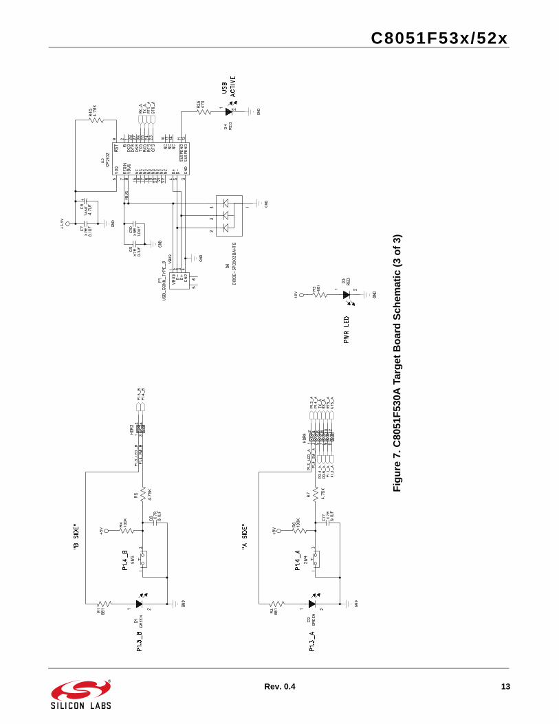
6. Schematics
Fig
ure
5.C
8051
F53
0A T
arg
et B
oar
d S
chem
atic
(1
of
3)

C8051F53x/52x
12 Rev. 0.4
Fig
ure
6.C
8051
F53
0A T
arg
et B
oar
d S
chem
atic
(2
of
3)
C8051F53x/52x
Rev. 0.4 13
Fig
ure
7.C
8051
F53
0A T
arg
et B
oar
d S
chem
atic
(3
of
3)

C8051F53x/52x
14 Rev. 0.4
DOCUMENT CHANGE LIST
Revision 0.2 to Revision 0.3 Updated for C8051F530A TB.
Added "LIN Connectivity (TB1)‚" on page 10.
Revision 0.3 to Revision 0.4 Updated "Software Setup‚" on page 2.
DisclaimerSilicon Laboratories intends to provide customers with the latest, accurate, and in-depth documentation of all peripherals and modules available for system and software implementers using or intending to use the Silicon Laboratories products. Characterization data, available modules and peripherals, memory sizes and memory addresses refer to each specific device, and "Typical" parameters provided can and do vary in different applications. Application examples described herein are for illustrative purposes only. Silicon Laboratories reserves the right to make changes without further notice and limitation to product information, specifications, and descriptions herein, and does not give warranties as to the accuracy or completeness of the included information. Silicon Laboratories shall have no liability for the consequences of use of the information supplied herein. This document does not imply or express copyright licenses granted hereunder to design or fabricate any integrated circuits. The products must not be used within any Life Support System without the specific written consent of Silicon Laboratories. A "Life Support System" is any product or system intended to support or sustain life and/or health, which, if it fails, can be reasonably expected to result in significant personal injury or death. Silicon Laboratories products are generally not intended for military applications. Silicon Laboratories products shall under no circumstances be used in weapons of mass destruction including (but not limited to) nuclear, biological or chemical weapons, or missiles capable of delivering such weapons.
Trademark InformationSilicon Laboratories Inc., Silicon Laboratories, Silicon Labs, SiLabs and the Silicon Labs logo, CMEMS®, EFM, EFM32, EFR, Energy Micro, Energy Micro logo and combinations thereof, "the world’s most energy friendly microcontrollers", Ember®, EZLink®, EZMac®, EZRadio®, EZRadioPRO®, DSPLL®, ISOmodem ®, Precision32®, ProSLIC®, SiPHY®, USBXpress® and others are trademarks or registered trademarks of Silicon Laboratories Inc. ARM, CORTEX, Cortex-M3 and THUMB are trademarks or registered trademarks of ARM Holdings. Keil is a registered trademark of ARM Limited. All other products or brand names mentioned herein are trademarks of their respective holders.
http://www.silabs.com
Silicon Laboratories Inc.400 West Cesar ChavezAustin, TX 78701USA
Simplicity Studio
One-click access to MCU and wireless tools, documentation, software, source code libraries & more. Available for Windows, Mac and Linux!
IoT Portfoliowww.silabs.com/IoT
SW/HWwww.silabs.com/simplicity
Qualitywww.silabs.com/quality
Support and Communitycommunity.silabs.com