capacitive power transfer for contactless...
TRANSCRIPT
Capacitive Power Transfer for Contactless Charging
Mitchell KlineIgor Izyumin
Prof. Bernhard BoserProf. Seth Sanders
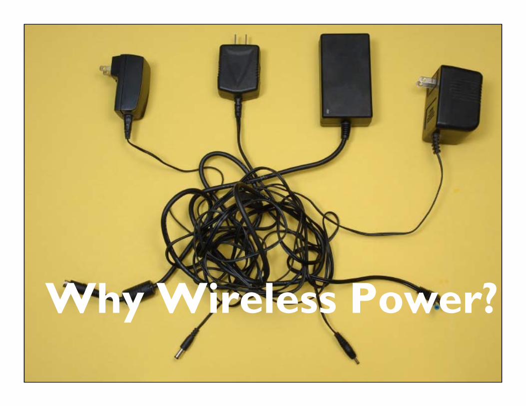
Why Wireless Power?
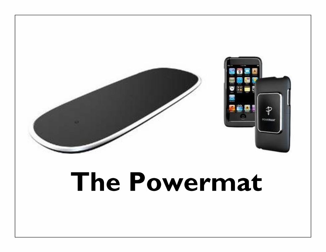
The Powermat
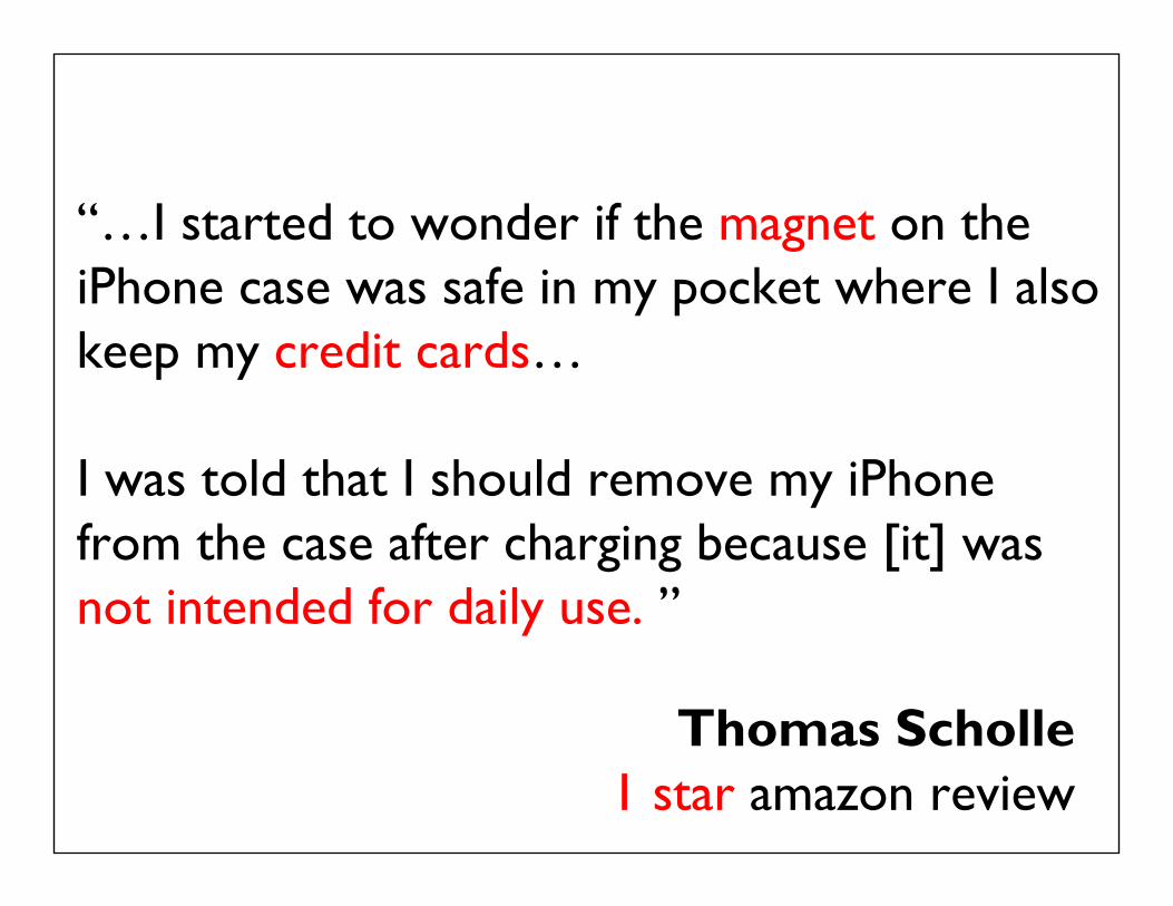
“…I started to wonder if the magnet on the iPhone case was safe in my pocket where I also keep my credit cards…
I was told that I should remove my iPhone from the case after charging because [it] was not intended for daily use. ”
Thomas Scholle1 star amazon review

“you'll need to invest another $40 per device to get the full functionality as you see it advertised. Too pricey for me!”
J. Lincoln2star amazon review
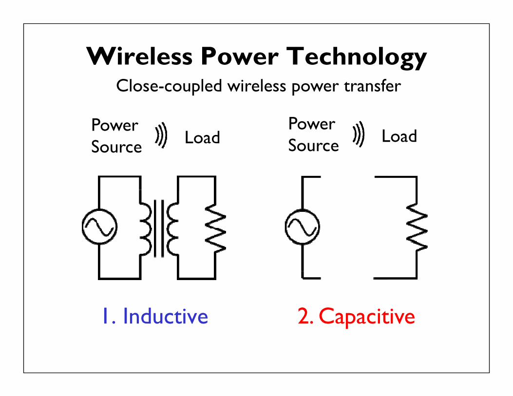
Wireless Power Technology
1. Inductive 2. Capacitive
Close-coupled wireless power transfer
Power Source Load
Power Source Load
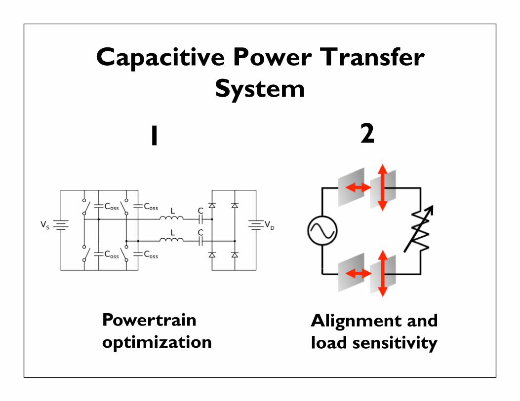
Capacitive Power Transfer System
Powertrainoptimization
Alignment and load sensitivity
1 2
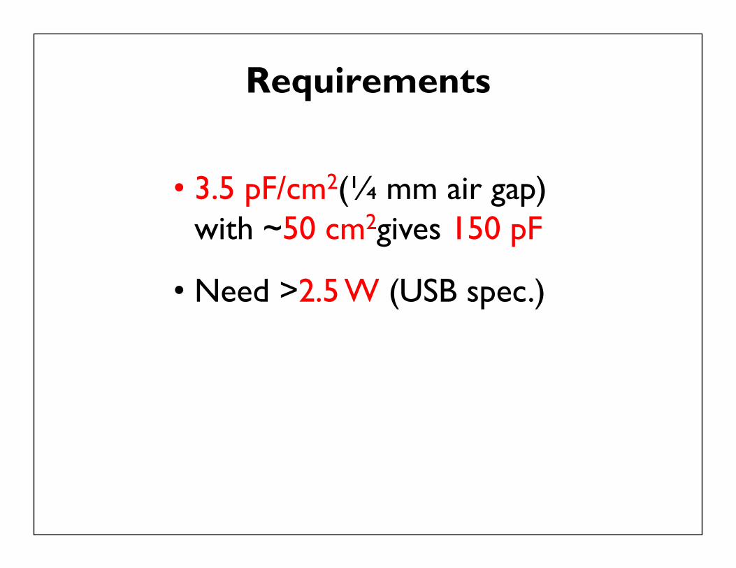
Requirements
• 3.5 pF/cm2(¼ mm air gap) with ~50 cm2gives 150 pF
• Need >2.5 W (USB spec.)
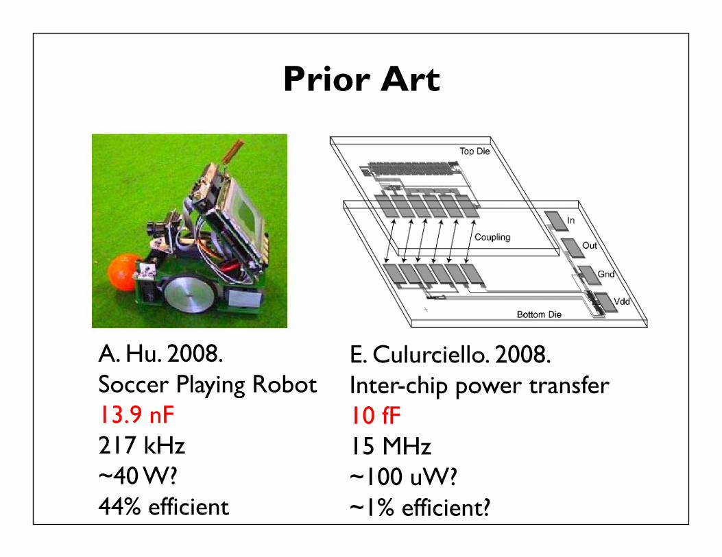
Prior Art
A. Hu. 2008.Soccer Playing Robot13.9 nF217 kHz~40 W?44% efficient
E. Culurciello. 2008.Inter-chip power transfer10 fF15 MHz~100 uW?~1% efficient?
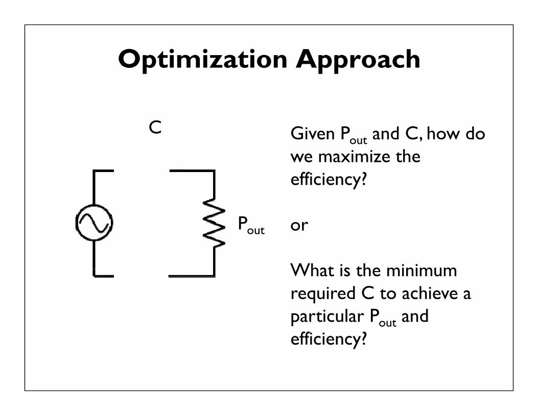
Optimization Approach
Given Pout and C, how do we maximize the efficiency?
or
What is the minimum required C to achieve a particular Pout and efficiency?
C
Pout
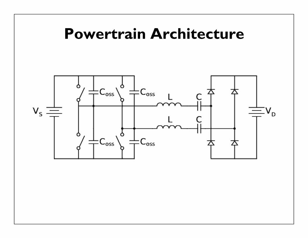
Powertrain Architecture
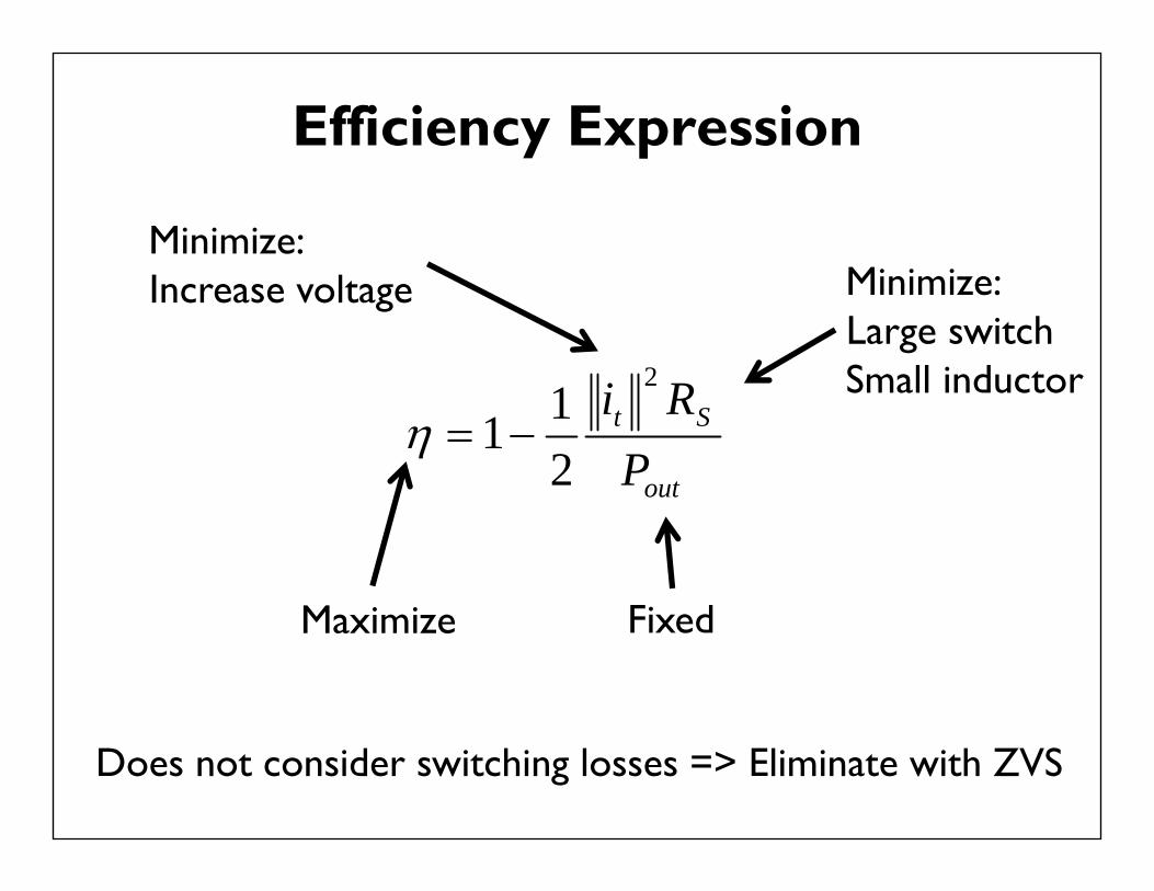
Efficiency Expression
Maximize Fixed
Minimize:Large switchSmall inductor
Minimize:Increase voltage
Does not consider switching losses => Eliminate with ZVS
out
St
PRi 2
211
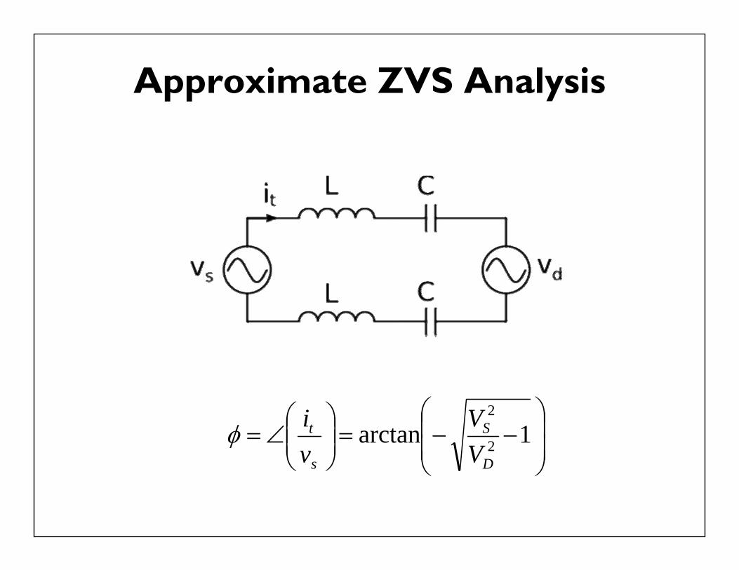
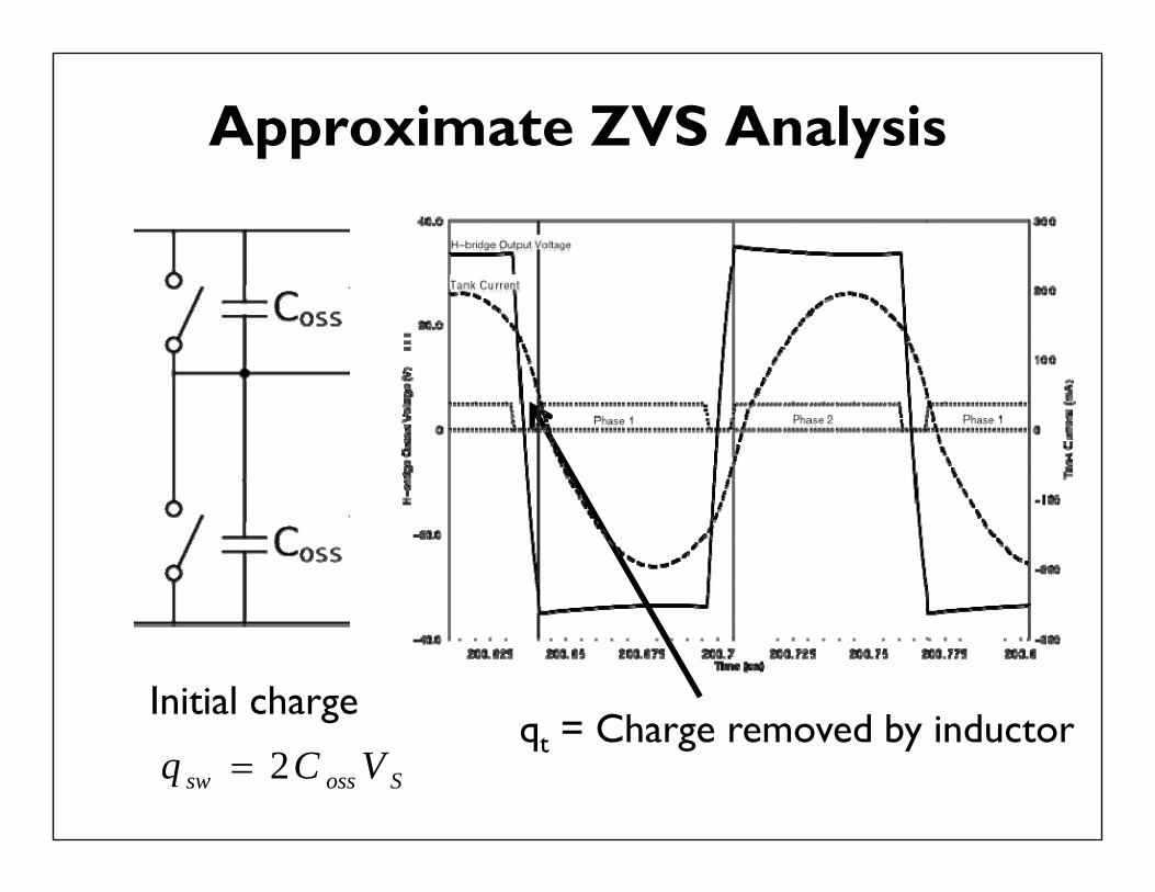
Approximate ZVS Analysis
1arctan 2
2
D
S
s
t
VV
vi
Approximate ZVS Analysis
Initial chargeqt = Charge removed by inductor
Sosssw VCq 2
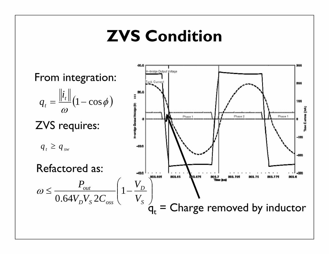
ZVS Condition
qt = Charge removed by inductor
From integration:
ZVS requires:
Refactored as:
cos1 tt
iq
swt qq
S
D
ossSD
out
VV
CVVP 1
264.0
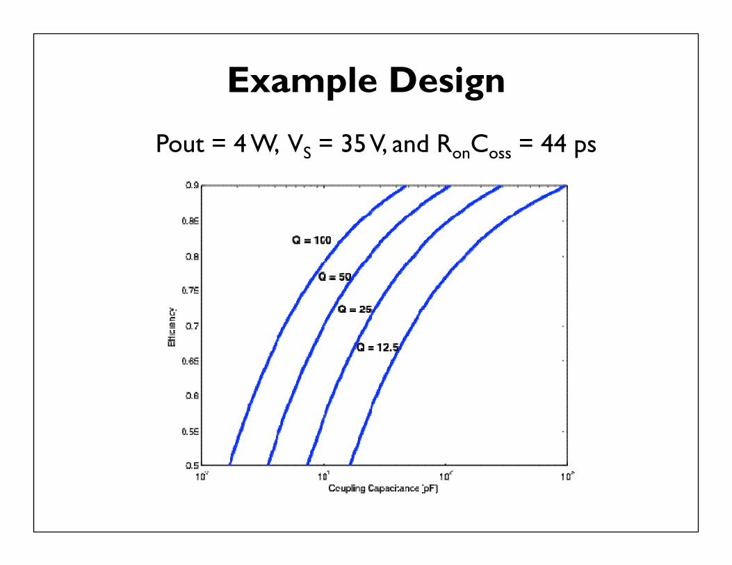
Example Design
Pout = 4 W, VS = 35 V, and RonCoss = 44 ps
Example Design
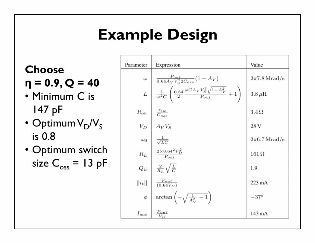
Choose η = 0.9, Q = 40• Minimum C is
147 pF• Optimum VD/VS
is 0.8• Optimum switch
size Coss = 13 pF
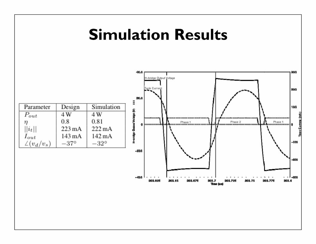
Simulation Results
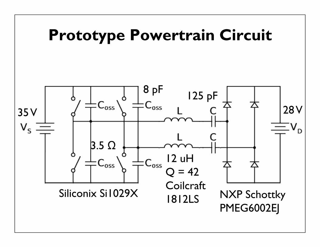
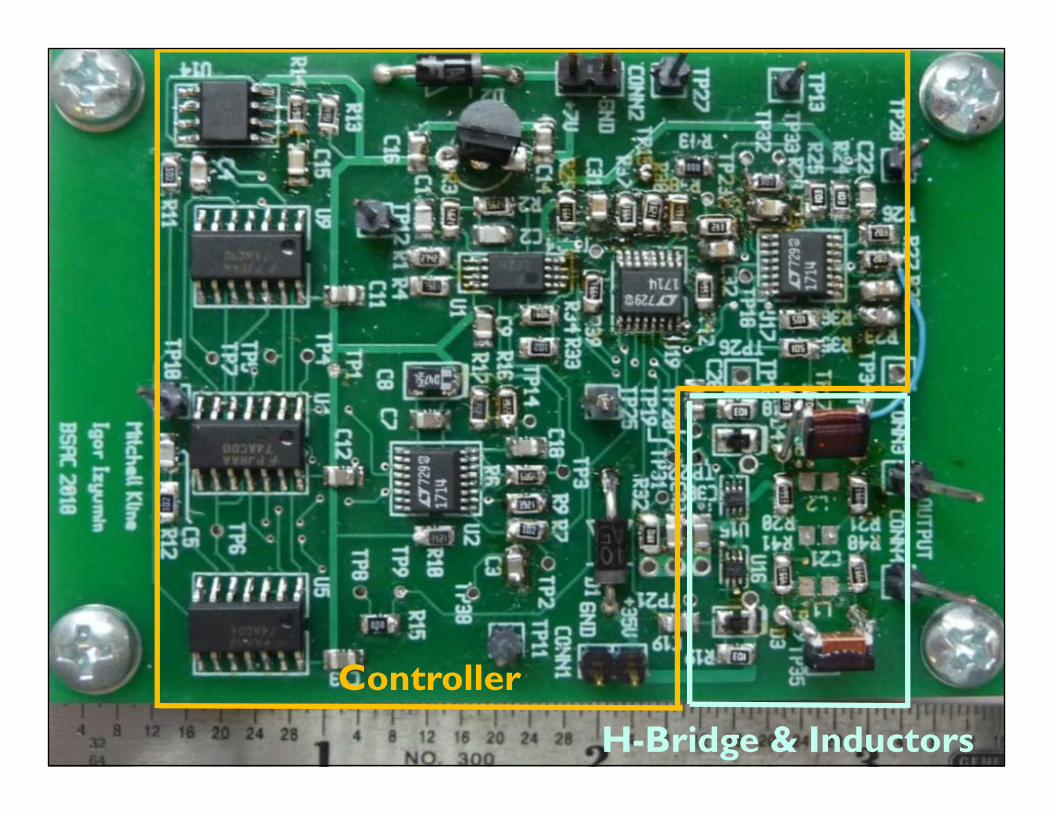
Prototype Powertrain Circuit
12 uHQ = 42Coilcraft1812LS
125 pF
NXP SchottkyPMEG6002EJ
Siliconix Si1029X
8 pF
3.5 Ω
35 V 28 V
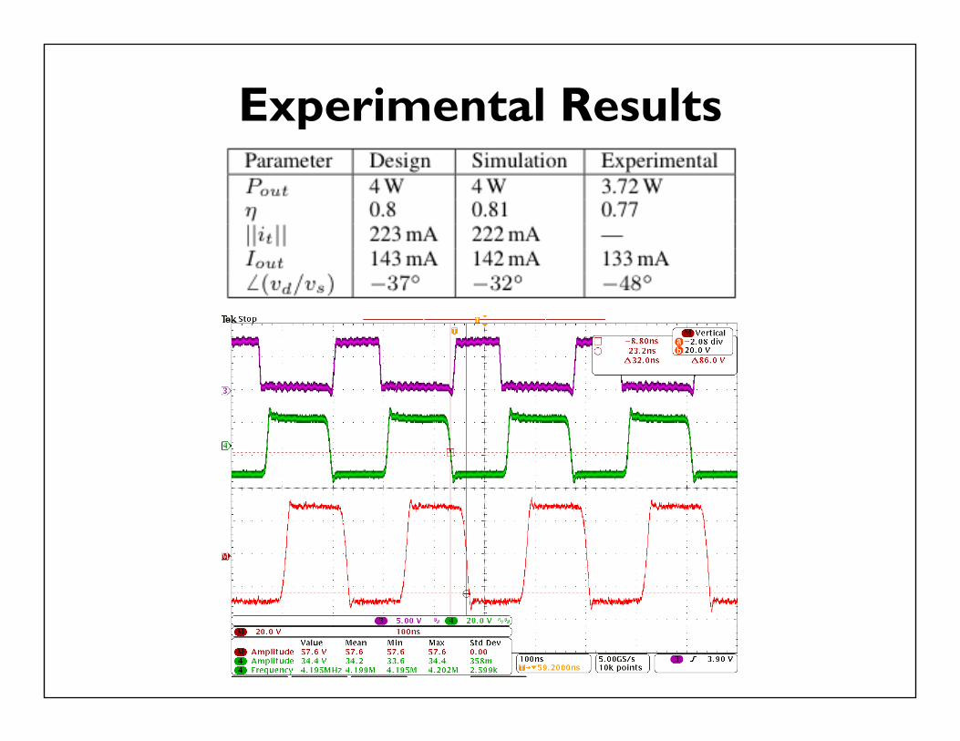
Experimental Results

Capacitive Power Transfer System
Powertrainoptimization
Alignment and load sensitivity
1 2
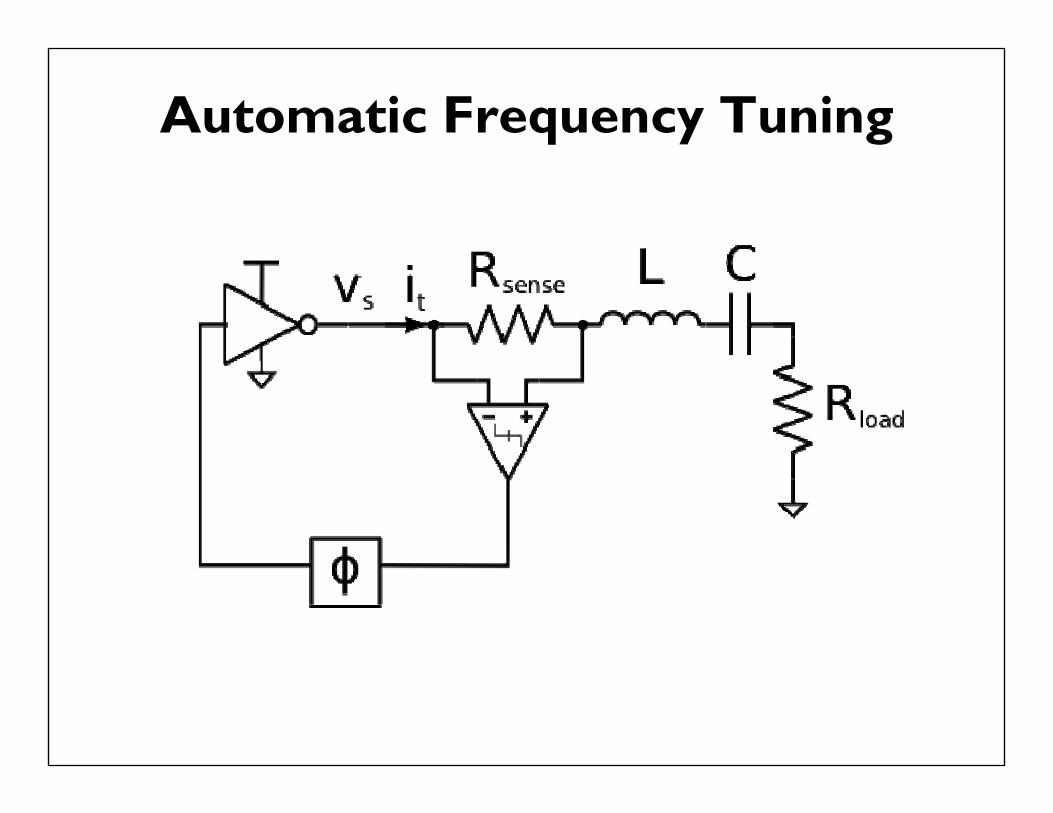
Automatic Frequency Tuning
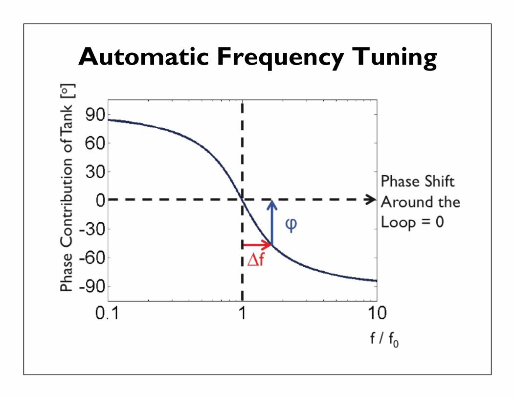
Automatic Frequency Tuning
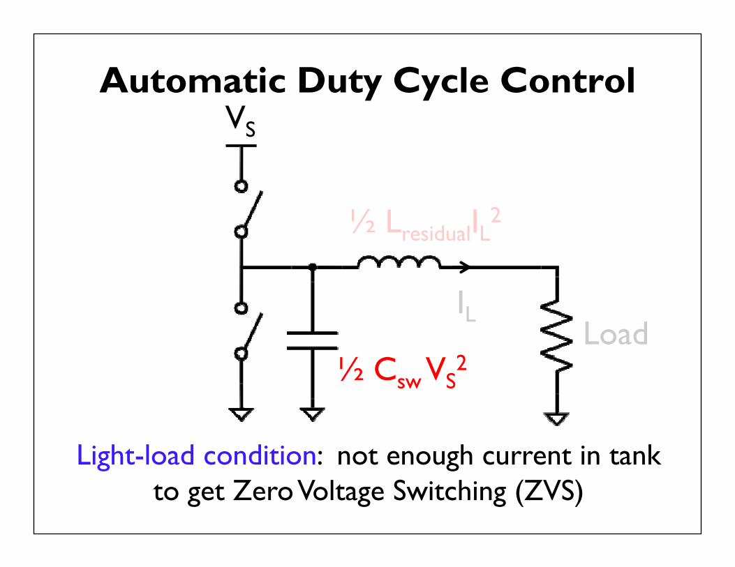
Automatic Duty Cycle Control
Light-load condition: not enough current in tank to get Zero Voltage Switching (ZVS)
VS
½ LresidualIL2
Load½ Csw VS
2
IL
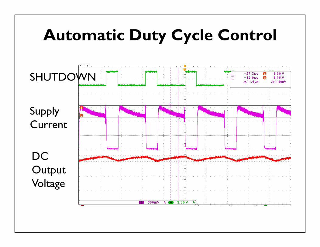
Automatic Duty Cycle Control
SHUTDOWN
Supply Current
DC Output Voltage
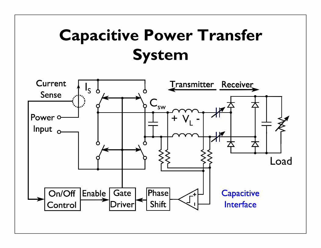
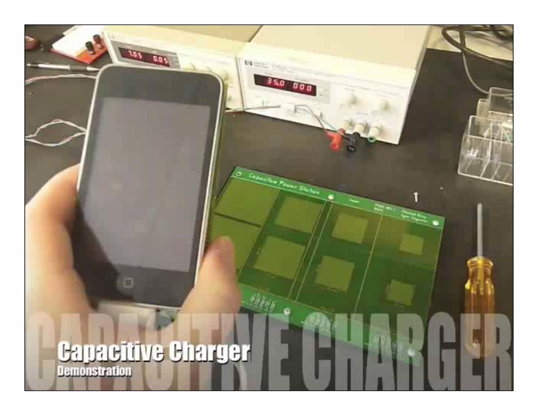
Capacitive Power Transfer System
IS
VL+ -Csw
Load
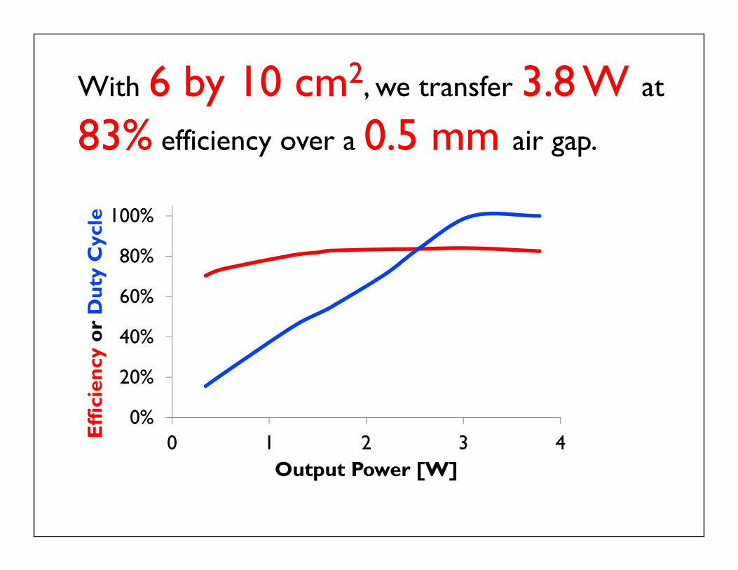
With 6 by 10 cm2, we transfer 3.8 W at
83% efficiency over a 0.5 mm air gap.
0%
20%
40%
60%
80%
100%
0 1 2 3 4Effi
cien
cyor
Dut
y C
ycle
Output Power [W]
Controller
H-Bridge & Inductors
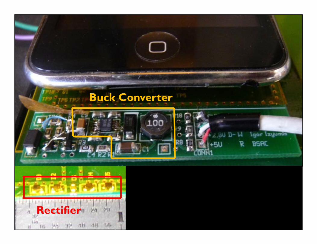
Buck Converter
Rectifier
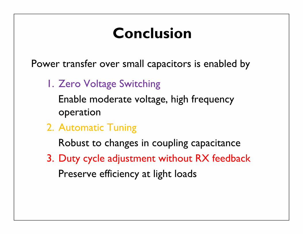
Conclusion
Power transfer over small capacitors is enabled by
1. Zero Voltage SwitchingEnable moderate voltage, high frequency operation
2. Automatic TuningRobust to changes in coupling capacitance
3. Duty cycle adjustment without RX feedbackPreserve efficiency at light loads

Thank You!
This material is based upon work supported by the
Defense Advanced Research Projects Agency (DARPA) under Contract No. W31P4Q-10-1-0002
AcknowledgementsDr. Mei-Lin ChanDr. Simone GambiniProf. David HorsleyDr. MischaMegensJames PengRichard PrzybylaKun WangProf. Ming Wu