carbon doping of self-organized tio 2 nanotube layers by thermal...
TRANSCRIPT

Carbon doping of self-organized TiO2 nanotube layers by thermal acetylene treatment
This article has been downloaded from IOPscience. Please scroll down to see the full text article.
2007 Nanotechnology 18 105604
(http://iopscience.iop.org/0957-4484/18/10/105604)
Download details:
IP Address: 142.103.160.110
The article was downloaded on 01/03/2013 at 09:13
Please note that terms and conditions apply.
View the table of contents for this issue, or go to the journal homepage for more
Home Search Collections Journals About Contact us My IOPscience
IOP PUBLISHING NANOTECHNOLOGY
Nanotechnology 18 (2007) 105604 (4pp) doi:10.1088/0957-4484/18/10/105604
Carbon doping of self-organized TiO2nanotube layers by thermal acetylenetreatmentRobert Hahn1, Andrei Ghicov1, Jarno Salonen2, Vesa-Pekka Lehto2
and Patrik Schmuki1,3
1 University of Erlangen-Nuremberg, Department of Materials Science and Engineering,Chair for Surface Science and Corrosion, WWIV-LKO, Martensstraße 7, D-91058 Erlangen,Germany2 Laboratory of Industrial Physics, Department of Physics, University of Turku, FIN-20014Turku, Finland
E-mail: [email protected]
Received 26 October 2006, in final form 19 December 2006Published 31 January 2007Online at stacks.iop.org/Nano/18/105604
AbstractSelf-organized layers of TiO2 nanotubes were formed by electrochemicalanodization of Ti in a HF/Na2HPO4 electrolyte. The tubes were treated at500 ◦C under a mixed flux of N2 and acetylene (C2H2). The samples werecharacterized using SEM, XRD and photoelectrochemical measurements.The results show that the acetylene treated tube layers exhibit a significantphotoresponse over the whole range of visible light up to the near-IR region(1.5 eV). This carbon doping treatment at comparable mild conditions doesnot lead to any structural damage to the morphology of the nanotubes.
1. Introduction
TiO2 is used for photocatalytic applications, due to theexcellent properties of TiO2 with respect to the correct band-gap position for water splitting, the degradation of organicsor direct light to electric energy conversion. Nevertheless,the large band-gap of 3.0–3.2 eV restricts these applicationsto use under UV light. To improve the efficiency of TiO2-based photon devices, several approaches were taken tomake the material sensitive to the visible range of light.Most common are dye sensitization [1, 2] or doping withsuitable elements [3–11]. Another important factor forphotocatalytic application is the surface area of the TiO2
electrodes. To produce a large surface area layers areusually formed by sintering TiO2 nanoparticles [12]. In thelast years a novel approach to achieving structures with ahigh surface area has attracted increasingly more interest:arrays consisting of highly ordered TiO2 nanotubes fabricatedby a simple electrochemical approach. Since the first-generation tubes reported by Zwilling et al [13] we haveshown several improvements in the aspect ratio by tailoringthe electrochemical conditions (e.g. pH [14–16] or by using‘non-aqueous’ electrolytes [17, 18]). These nanotubular layers
3 Author to whom any correspondence should be addressed.
have attracted much attention in the fields of catalytic [19],wetting [20] and biomedical applications [21]. Apart fromdye senzitisation [22], we recently reported successful nitrogendoping of the nanotubes combined with a significant increasein the visible photoresponse by thermal treatment in anammonia environment [23] or nitrogen-ion implantation [24].An element reported to be of similar efficiency to nitrogenin improving the photoresponse of TiO2 is carbon. This istypically achieved by flame annealing, hydrolysis of fittingcompounds or treatment in CO [25–27]. In the present work,we have investigated carbon doping of TiO2 nanotubes by amild thermal acetylene treatment previously used, for example,to stabilize porous silicon [28].
2. Experimental details
Titanium foils (99.6% purity) with a thickness of 0.1 mm weresonicated in acetone, isopropanol and methanol for severalminutes, followed by rinsing with deionized water and dryingunder a N2 stream. Highly ordered nanotube layers were grownby anodization of the samples in 1 M (Na2HPO4) + 0.3 wt%HF electrolyte by ramping from the open-circuit potential to20 V in 50 mV s−1 steps and holding the potential for 2 h. Forthis a computer controlled set-up using a Jaissle IMP 88 PC
0957-4484/07/105604+04$30.00 1 © 2007 IOP Publishing Ltd Printed in the UK

Nanotechnology 18 (2007) 105604 R Hahn et al
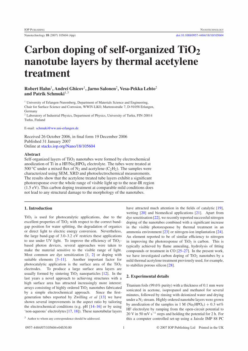
Figure 1. SEM top view and cross-section (inset) of TiO2 nanotubesformed anodically in 1 M Na2HPO4 + 0.3 wt% HF electrolyte at20 V for 2 h and carbonized at 500 ◦C in acetylene/N2 atmosphere.
high-voltage potentiostat was employed. The electrochemicalexperiments were carried out at room temperature in a cell witha three-electrode arrangement. The samples were contactedwith a Cu back-plate (as the working electrode) and thenpressed against an O-ring opening in the wall of the cell,leaving an exposed area of 1 cm2. A Pt gauze served ascounter electrode and an Ag/AgCl electrode connected to aHaber–Luggin capillary was used as a reference electrode.After anodization, the samples were rinsed with deionizedwater and dried in a nitrogen stream. Some samples wereannealed to form an anatase crystal structure using a rapidthermal annealer (Jipelec Jet First 100) at 450 ◦C for 1 h in air.For the characterization of the sample morphology a HitachiFE-SEM S4800 field-emission scanning electron microscopewas used. Carbon doping of the TiO2 layer was carried outby heating amorphous and anatase samples at 500 ◦C in aquartz tube under a continuous N2 flux to which an acetylene(C2H2) flux (1:1) was added 15 min prior to the thermaltreatment at room temperature and also during the 10 mintreatment. The treated TiO2 nanotube layers were cooleddown to room temperature under a N2 flow before contactwith ambient air. To examine the crystalline structure of thetreated samples, XRD measurements were performed usingCu Kα radiation with an X‘pert Philips MPD PW 3040. Thechemical composition of the samples was characterized byx-ray photoelectron spectroscopy (PHI 5600 XPS) using AlKα monochromatized radiation. The C1s peak at 284.8 eVwas used to assess carbon uptake. Photoelectrochemicalmeasurements were recorded with a lock-in amplifier/chopperset-up (using a chopper frequency of 30 Hz) including anOriel 6356 150 W Xe arc lamp as the light source and anOriel cornerstone 7400 1/8 monochromator. Photocurrenttransients were recorded at 500 nm using a mechanical shuttersystem. All photocurrent measurements were carried out in0.1 M Na2SO4 at an applied potential of 0.5 V (three electrodeconfiguration: Ag/AgCl as the reference electrode and Pt as thecounter electrode) in an electrochemical cell equipped with aquartz glass window.
3. Results and discussion
Figure 1 shows SEM images (top view and a cross-sectionas inset) of the TiO2 nanotubular arrays after the acetylene
Figure 2. XRD spectra of samples annealed at 450 and 500 ◦C in airand of a sample after the carbonization procedure at 500 ◦C inacetylene/nitrogen.
treatment. The morphology is identical to images taken priorto the heat treatment with tubes with an average tube diameterof 100 nm and an approximate length of 1.1 μm. Froma comparison it is evident that this treatment is negligiblydestructive to the morphology of the tubes and thereforemore suitable for carbon doping of titanium dioxide than, forexample, flame annealing approaches. Figure 2 shows the x-ray diffraction spectra of samples annealed at 450 and 500 ◦Cin air, and of a sample after the carbonization procedure at500 ◦C in acetylene/nitrogen. It has been reported that carbonincorporated in the TiO2 structure can suppress the anatase–rutile phase transition [29]. This effect is also present inthese XRD measurements. Here annealing at 500 ◦C in air,in contrast to doping conditions at 500 ◦C in acetylene/N2,already leads to some rutile formation. For better comparison aXRD spectrum of purely anatase starting material (nanotubulararrays annealed at 450 ◦C in air) is also shown. To gain moreinformation about the changes in the chemical compositionduring thermal treatment, XPS spectra were taken of a flat,compact, anodic (20 V) TiO2 layer carbonized under sameconditions. The determined XPS peaks shows a significantcarbon uptake (∼48 at.%, 45◦). By changing the incidentangle of the x-ray beam from 15◦ to 75◦ the detected carboncontent decreased from 60 to 37 at.% (implying surface dopingeffects rather than bulk doping). Figure 3 presents normalizedphotocurrent spectra from 370 to 800 nm of two carbon-doped samples. The difference of both samples is the startingstructure before the acetylene treatment. One was originalas-grown amorphous and the other one was pre-annealed toanatase. The graphs show only a slightly higher photocurrentfor the anatase starting structure. XRD measurements revealedthat the amorphous structure also turned to anatase during thecarbonization process. To demonstrate the efficiency of thecarbon-doping effect in the whole range of visible light (tonear IR) the photocurrent of an undoped anatase nanotubularlayer is also included in the figure. The inset shows aband-gap determination of the carbon-doped TiO2 nanotubulararray from the ( jphhν)1/2 versus energy plot. Clearly, thebehaviour exhibits two linear parts. One delivers the band-gap onset energy of anatase TiO2 at 3.16 eV. The other
2

Nanotechnology 18 (2007) 105604 R Hahn et al
Figure 3. Photocurrent spectra of the anatase TiO2 nanotubular layerbefore C doping, a carbonized as-grown amorphous sample and acarbonized, but pre-annealed to anatase, sample. The inset shows aband-gap determination of the carbon-doped TiO2 nanotubular arrayfrom the ( jphhν)1/2 versus energy plot.
Figure 4. Photocurrent transients of a carbonized as-grownamorphous sample and a carbonized, pre-annealed to anatase, TiO2
nanotubular layer.
one shows the deep photocurrent response down to 1.5 eVas the result of carbon doping. In order to obtain moredetailed information about the differences between amorphousor anatase structure as the starting material, some photocurrenttransients were taken at λ = 500 nm with a 10 s light pulse(figure 4). The transients revealed that besides the higher totalphotocurrent values of anatase starting material, the decaykinetics is also different. This can be ascribed to the energyof light with a 500 nm wavelength being far away from thebandgap energy of anatase TiO2 and therefore the influenceof reactions (e.g. recombination, trapping, detrapping andhopping) over states inside the bandgap (C doping) becomespredominant. The observed negative photocurrent, when thelight is switched off, may be ascribed to reaction of chargecarriers and detrapping of counter charge [30]. This resultsuggests that pre-annealing to anatase before carbonization
leads to fewer defect states in the structure and therefore tohigher photocurrents and a lower recombination rate of thecharge carriers.
4. Conclusion
TiO2 nanotubular layers were successfully doped with carbonusing a non-destructive thermal treatment at 500 ◦C undera mixed flux of N2 and acetylene. The results show thatthis heating approach using anatase starting material is verypromising for achieving a significant photocurrent response inthe whole range of visible light. This and the high surfacearea of the self-organized TiO2 nanotubes can increase theefficiency of TiO2-based photocatalytic devices.
Acknowledgments
The author would like to acknowledge Anja Friedrich for SEM,Ulrike Marten-Jahns for XRD, Helga Hildebrand for XPS andthe DFG for financial support.
References
[1] O’Regan B and Gratzel M 1991 Nature 353 737[2] Hagfeldt A and Gratzel M 1995 Chem. Rev. 95 49[3] Hoffmann M R, Martin S T, Choi W and Bahnemannt D W
1995 Chem. Rev. 95 69[4] Anpo M 1997 Catal. Surv. Japan 1 169[5] Sakthivel S and Kisch H 2003 Angew. Chem. Int. Edn 42 4908[6] Ohno T, Mitsui T and Matsumura M 2003 Chem. Lett. 32 364[7] Umebayashi T, Yamaki T, Tanaka S and Asai K 2003 Chem.
Lett. 32 330[8] Lin L, Lin W, Zhu Y, Zhao B and Xie Y 2005 Chem. Lett.
34 284[9] Yamaki T, Umebayashi T, Sumita T, Yamamoto S,
Maekawa M, Kawasuso A and Itoh H 2003 Nucl. Instrum.Methods B 206 254
[10] Zhao W, Ma W, Chen C, Zhao J and Shuai Z 2004 J. Am.Chem. Soc. 126 4782
[11] Yang M C, Yang T S and Wong M S 2004 Thin Solid Films 1–5469
[12] Gratzel M 2003 J. Photochem. Photobiol. C 4 145[13] Zwilling V, Darque-Ceretti E, Boutry-Forveille A, David D,
Perrin M Y and Aucouturier M 1999 Surf. Interface Anal.27 629
[14] Macak J M, Sirotna K and Schmuki P 2005 Electrochim. Acta50 3679
[15] Macak J M, Tsuchiya H and Schmuki P 2005 Angew. Chem.Int. Edn 44 2100
[16] Ghicov A, Tsuchiya H, Macak J M and Schmuki P 2005Electrochem. Commun. 7 505
[17] Macak J M, Tsuchiya H, Taveira L, Aldabergerova S andSchmuki P 2005 Angew. Chem. Int. Edn 44 7463
[18] Albu S, Ghicov A, Macak J M and Schmuki P 2007 Phys. Stat.Sol. (RRL) 1 R65–7
[19] Macak J M, Tsuchiya H, Ghicov A and Schmuki P 2005Electrochem. Commun. 7 1133
[20] Balaur E, Macak J M, Taveira L and Schmuki P 2005Electrochem. Commun. 7 1066
[21] Tsuchiya H, Macak Jan M, Muller L, Kunze J, Muller F,Greil P, Virtanen S, Schmuki P and Biomed J 2006 Mater.Res. A 77 534
[22] Macak J M, Tsuchiya H, Ghicov A and Schmuki P 2005Electrochem. Commun. 7 1133
[23] Vitiello R P, Macak J M, Ghicov A, Tsuchiya H, Dick L F Pand Schmuki P 2006 Electrochem. Commun. 8 544
3

Nanotechnology 18 (2007) 105604 R Hahn et al
[24] Ghicov A, Macak J M, Tsuchiya H, Kunze J,Haeublein V, Frey L and Schmuki P 2006 Nano Lett.6 1080
[25] Shankar K, Paulose M, Mor G K, Varghese O K andGrimes C A 2005 Ann. Phys., Lpz. 38 3543
[26] Neumann B, Bogdanoff P, Tributsch H, Sakthivel S andKisch H 2005 J. Phys. Chem. B 109 16579
[27] Park J H, Kim S and Bard A J 2006 Nano Lett. 6 24[28] Salonen J, Bjorkqvist M, Laine E and Niinisto L 2004 Appl.
Surf. Sci. 225 389[29] Enache C S, Schoonman J and Van de Krol R 2006 Appl. Surf.
Sci. 252 6342[30] Bube R H 1992 Photoelectronic Properties of Semiconductors
(Cambridge: Cambridge University Press)
4