challenges in lithographic patterning of electronics structures on flexible substrates · ·...
TRANSCRIPT
January 29, 2008
Challenges in lithographic patterning of electronics structures on flexible substrates
Advanced Lithography conference, San Jose, 27 February 2008
Erwin R. Meinders
Contact: [email protected]
TP6 Lithography on flexible substrates, status wk804, E.R. Meinders, Confidential
� 2© Holst Centre
Contents
• Introduction Holst centre
• Introduction ‘lithography on flexible substrates’ program
• Results
� Foil characterization
� Handling of flexible substrates
� Imaging characteristics
� Transistor-on-foil demonstrator
• Conclusions
TP6 Lithography on flexible substrates, status wk804, E.R. Meinders, Confidential
� 3© Holst Centre
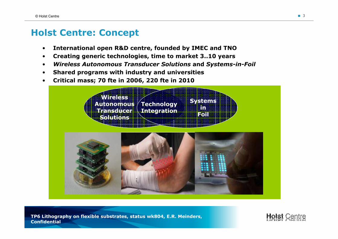
Holst Centre: Concept
Wireless Autonomous Transducer Solutions
SystemsinFoil
Technology Integration
© Holst Centre
• International open R&D centre, founded by IMEC and TNO
• Creating generic technologies, time to market 3..10 years
• Wireless Autonomous Transducer Solutions and Systems-in-Foil
• Shared programs with industry and universities
• Critical mass; 70 fte in 2006, 220 fte in 2010
TP6 Lithography on flexible substrates, status wk804, E.R. Meinders, Confidential
� 4© Holst Centre
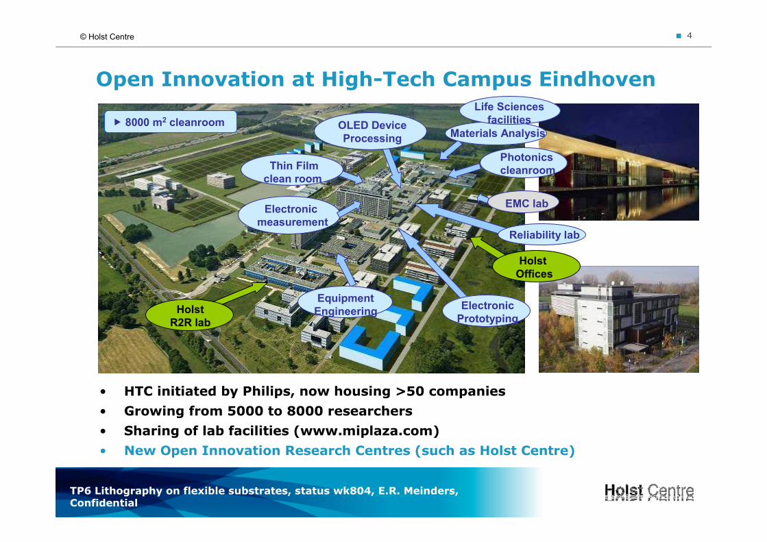
• HTC initiated by Philips, now housing >50 companies
• Growing from 5000 to 8000 researchers
• Sharing of lab facilities (www.miplaza.com)
• New Open Innovation Research Centres (such as Holst Centre)
Open Innovation at High-Tech Campus Eindhoven
Materials Analysis
Electronic
measurement
Thin Film
clean room
OLED Device
Processing
Reliability lab
Photonics
cleanroom
Electronic
Prototyping
� 8000 m2 cleanroom
Equipment
Engineering
Life Sciences
facilities
EMC lab
Holst
R2R lab
Holst
Offices
TP6 Lithography on flexible substrates, status wk804, E.R. Meinders, Confidential
� 5© Holst Centre
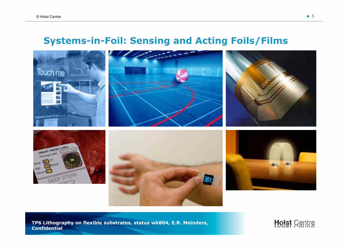
Systems-in-Foil: Sensing and Acting Foils/Films
TP6 Lithography on flexible substrates, status wk804, E.R. Meinders, Confidential
� 6© Holst Centre
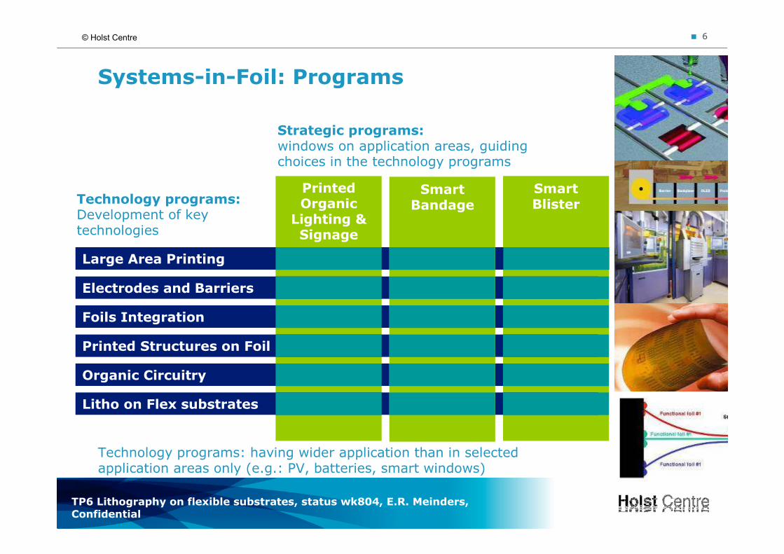
Litho on Flex substrates
Large Area Printing
Foils Integration
Printed Structures on Foil
Organic Circuitry
Electrodes and Barriers
Smart BlisterTechnology programs:
Development of key technologies
Strategic programs:windows on application areas, guiding choices in the technology programs
Printed Organic
Lighting & Signage
Systems-in-Foil: Programs
Smart Bandage
Technology programs: having wider application than in selected application areas only (e.g.: PV, batteries, smart windows)
TP6 Lithography on flexible substrates, status wk804, E.R. Meinders, Confidential
� 7© Holst Centre
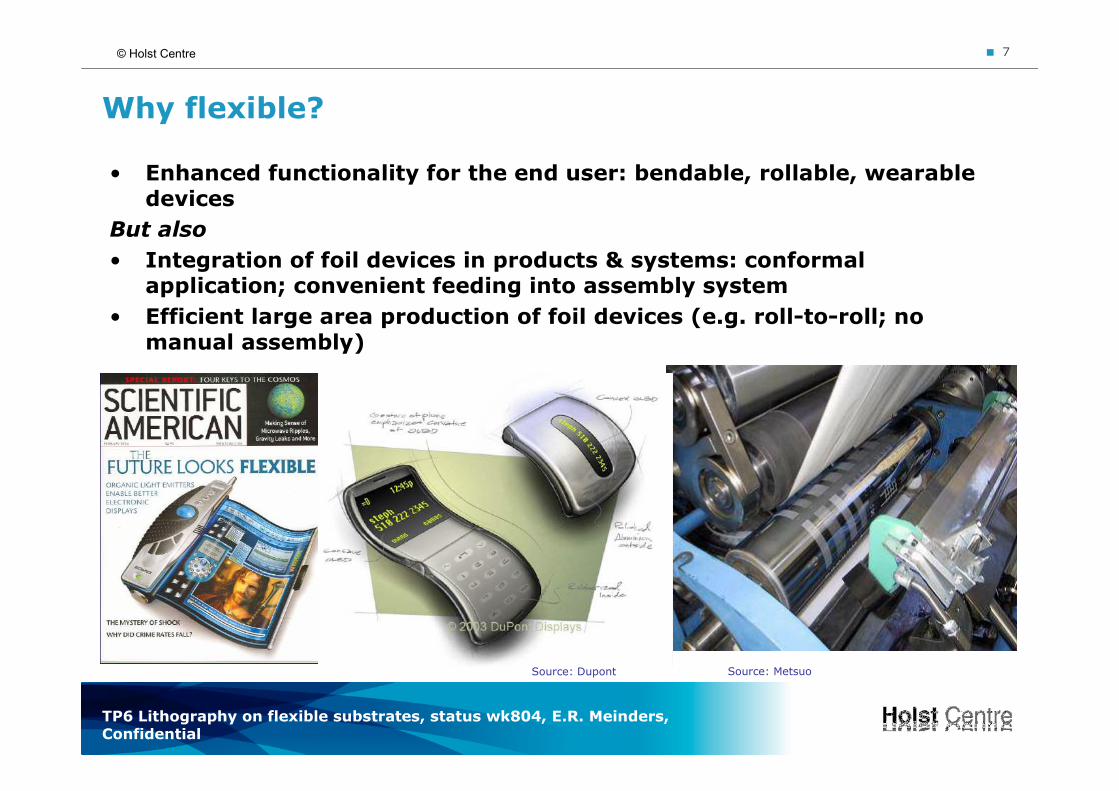
Why flexible?
• Enhanced functionality for the end user: bendable, rollable, wearable devices
But also
• Integration of foil devices in products & systems: conformal application; convenient feeding into assembly system
• Efficient large area production of foil devices (e.g. roll-to-roll; no manual assembly)
Source: Dupont Source: Metsuo
TP6 Lithography on flexible substrates, status wk804, E.R. Meinders, Confidential
� 8© Holst Centre
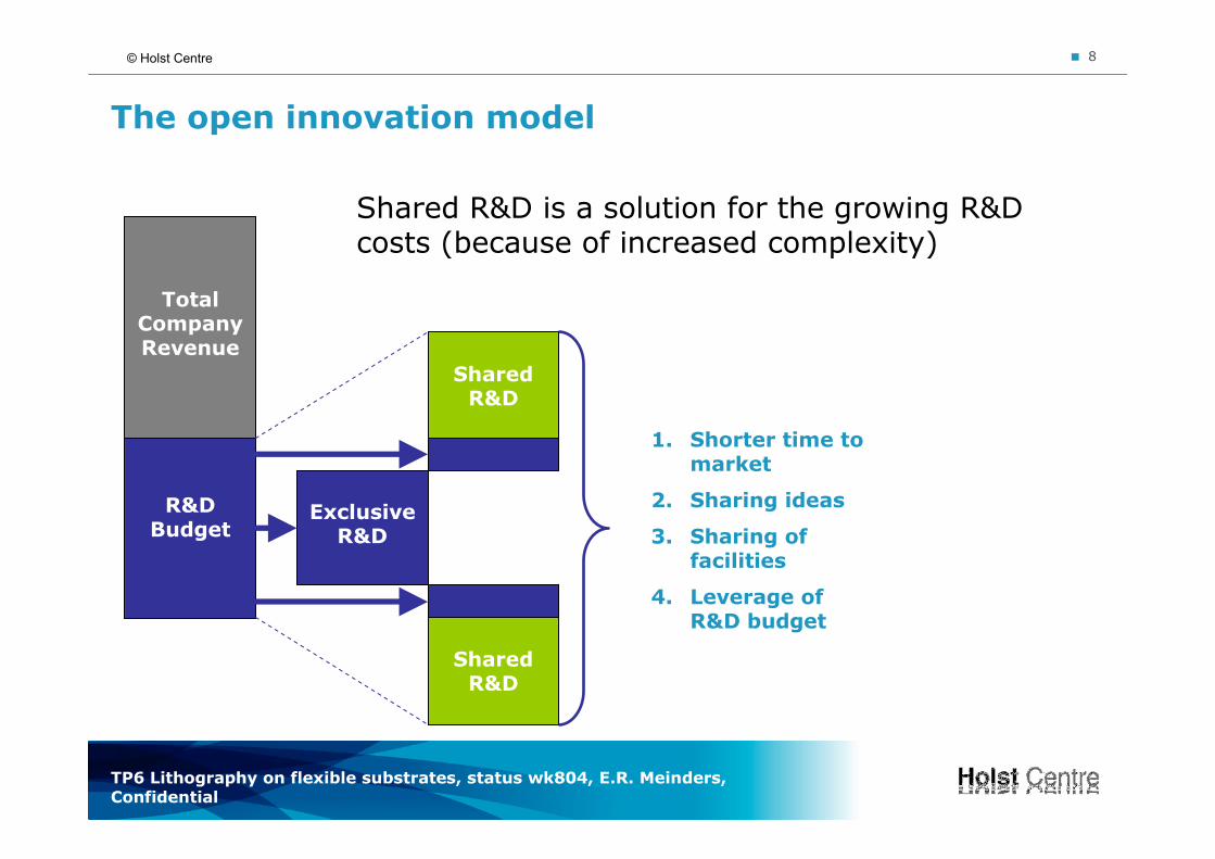
The open innovation model
Shared R&D is a solution for the growing R&D costs (because of increased complexity)
Total Company Revenue
R&D Budget
Shared R&D
ExclusiveR&D
Shared R&D
1. Shorter time to market
2. Sharing ideas
3. Sharing of facilities
4. Leverage of R&D budget
January 29, 2008
Lithography on flexible substrates
Status technology program ‘Lithography on flexible substrates’
Erwin R. Meinders, Eindhoven, February 2008
TP6 Lithography on flexible substrates, status wk804, E.R. Meinders, Confidential
� 10© Holst Centre
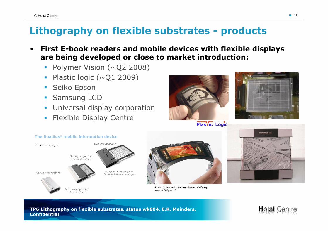
Lithography on flexible substrates - products
• First E-book readers and mobile devices with flexible displays are being developed or close to market introduction:
� Polymer Vision (~Q2 2008)
� Plastic logic (~Q1 2009)
� Seiko Epson
� Samsung LCD
� Universal display corporation
� Flexible Display Centre
TP6 Lithography on flexible substrates, status wk804, E.R. Meinders, Confidential
� 11© Holst Centre
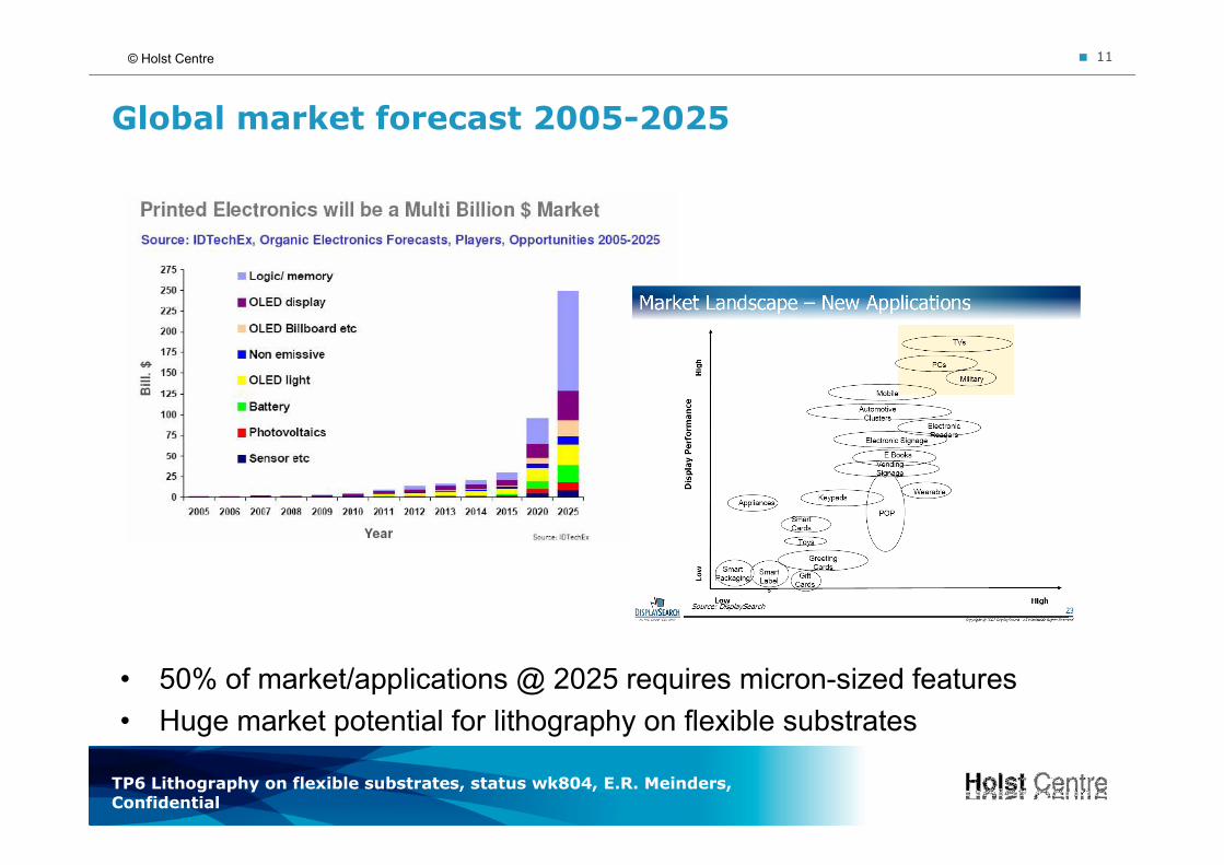
Global market forecast 2005-2025
• 50% of market/applications @ 2025 requires micron-sized features
• Huge market potential for lithography on flexible substrates
TP6 Lithography on flexible substrates, status wk804, E.R. Meinders, Confidential
� 12© Holst Centre
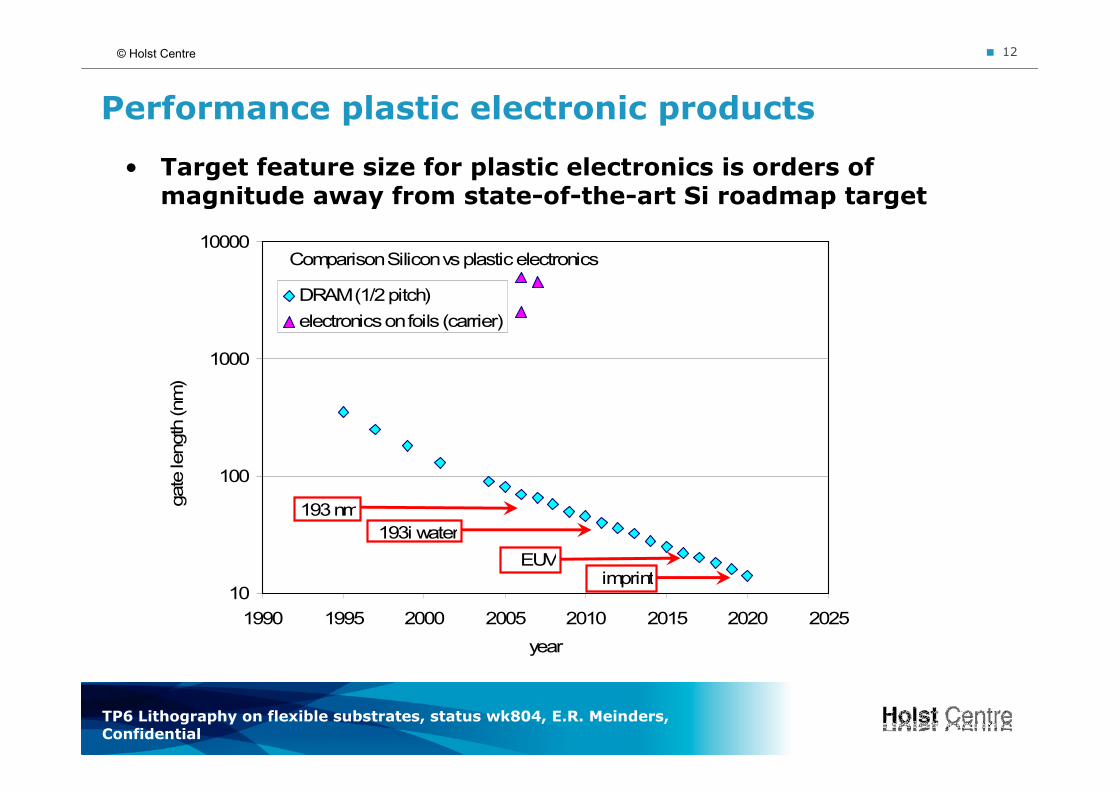
Performance plastic electronic products
• Target feature size for plastic electronics is orders of magnitude away from state-of-the-art Si roadmap target
Comparison Silicon vs plastic electronics
10
100
1000
10000
1990 1995 2000 2005 2010 2015 2020 2025
year
gate length (nm) cd DRAM (1/2 pitch)
electronics on foils (carrier)
193 nm
193i water
EUVimprint
TP6 Lithography on flexible substrates, status wk804, E.R. Meinders, Confidential
� 13© Holst Centre
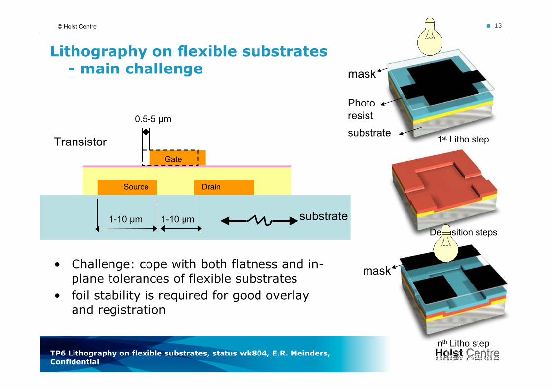
Lithography on flexible substrates - main challenge
• Challenge: cope with both flatness and in-plane tolerances of flexible substrates
• foil stability is required for good overlay and registration
0.5-5 µm
Gate
1-10 µm
DrainSource
1-10 µm substrate
nth Litho step
mask
Deposition steps
mask
Photo
resist
substrate1st Litho stepTransistor
TP6 Lithography on flexible substrates, status wk804, E.R. Meinders, Confidential
� 14© Holst Centre
TP6 ‘lithography on flexible substrates’
Program objectives:
• Develop lithography technology for manufacturing of electronic circuitry on flexible substrates with (sub)-micron sized features.
• Develop technology together with all program partners (ASML, Philips, Bekaert, Singulus Mastering, Polymer Vision, TNO, IMEC, Mesa+)
Batch-to-batch, foil-on-carrier lithography:
• Feature size 1-10 µm, overlay accuracy < 1 µm.
• Use of mature optical lithography technology (MA6, PAS5500, etc).
• Foil-on-carrier approach for substrate handling.
Large area lithography:
• Develop a large-area, low-cost lithography technology for patterning of 2.5µm features for electronic applications on flexible substrates.
• Decisions need to be made with respect to equipment, lithographyprocess, substrate handling, etc.
TP6 Lithography on flexible substrates, status wk804, E.R. Meinders, Confidential
� 15© Holst Centre
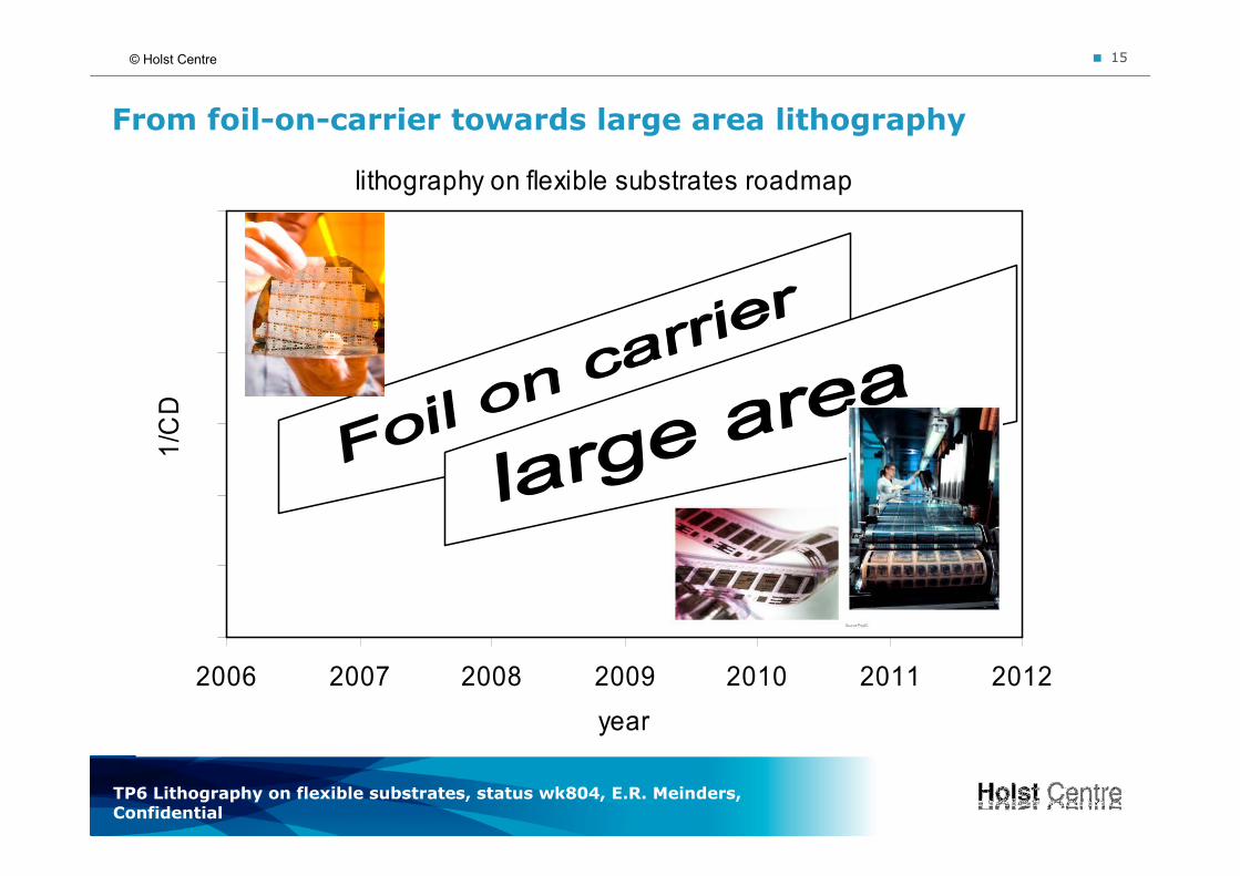
From foil-on-carrier towards large area lithography
lithography on flexible substrates roadmap
2006 2007 2008 2009 2010 2011 2012
year
1/CD
TP6 Lithography on flexible substrates, status wk804, E.R. Meinders, Confidential
� 16© Holst Centre
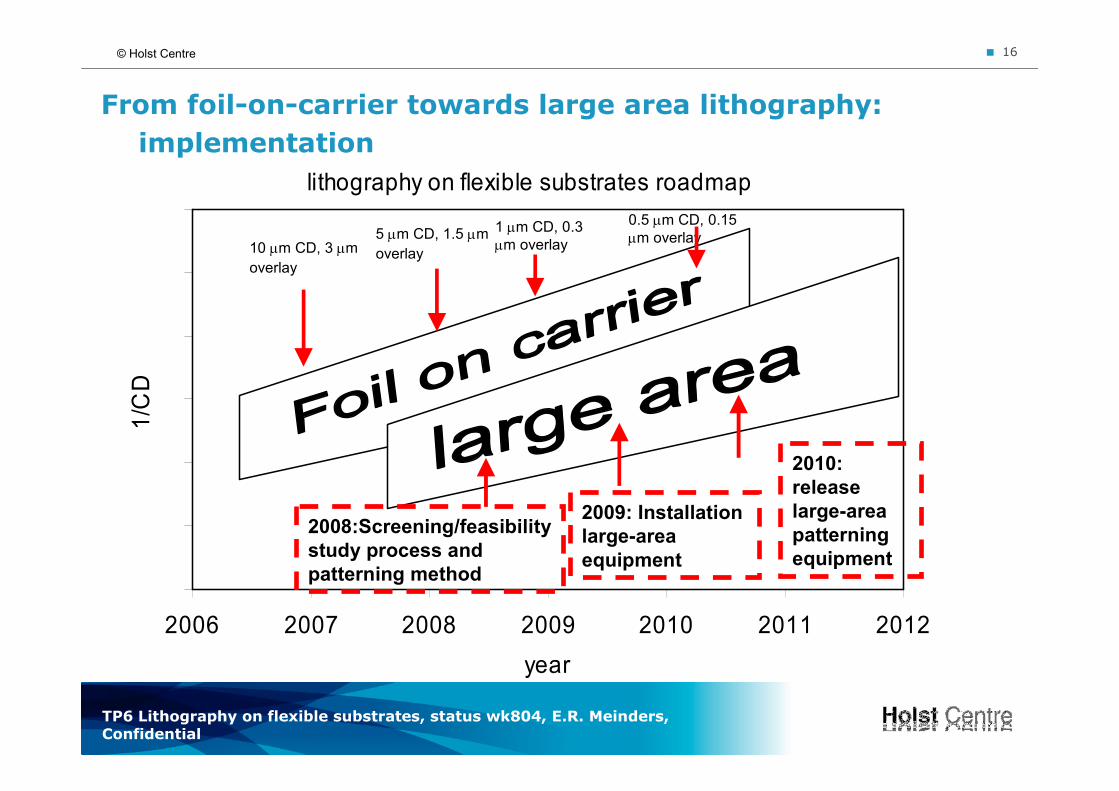
From foil-on-carrier towards large area lithography:
implementation
lithography on flexible substrates roadmap
2006 2007 2008 2009 2010 2011 2012
year
1/CD
5 µm CD, 1.5 µm
overlay
1 µm CD, 0.3
µm overlay
0.5 µm CD, 0.15
µm overlay
2008:Screening/feasibility
study process and
patterning method
2010:
release
large-area
patterning
equipment
2009: Installation
large-area
equipment
10 µm CD, 3 µm
overlay
TP6 Lithography on flexible substrates, status wk804, E.R. Meinders, Confidential
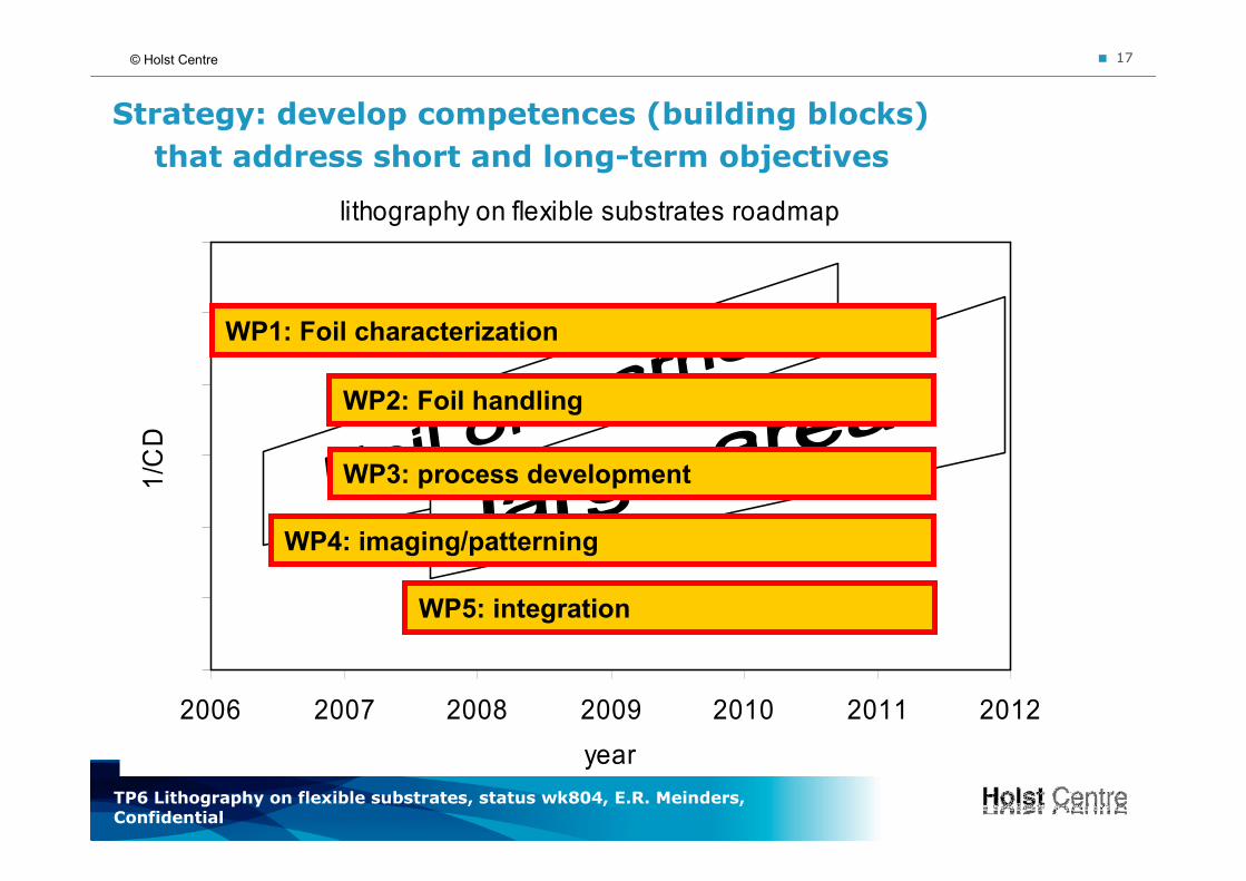
� 17© Holst Centre
Strategy: develop competences (building blocks)
that address short and long-term objectives
lithography on flexible substrates roadmap
2006 2007 2008 2009 2010 2011 2012
year
1/CD
WP1: Foil characterization
WP2: Foil handling
WP3: process development
WP4: imaging/patterning
WP5: integration
TP6 Lithography on flexible substrates, status wk804, E.R. Meinders, Confidential
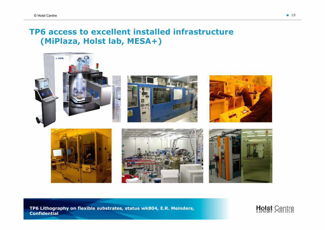
� 18© Holst Centre
TP6 access to excellent installed infrastructure (MiPlaza, Holst lab, MESA+)
January 29, 2008
Results
- foil characterization
- handling of flexible substrates
- imaging characteristics
- demonstrator
Status technology program ‘Lithography on flexible substrates’
Erwin R. Meinders, Eindhoven, February 2008
TP6 Lithography on flexible substrates, status wk804, E.R. Meinders, Confidential
� 20© Holst Centre
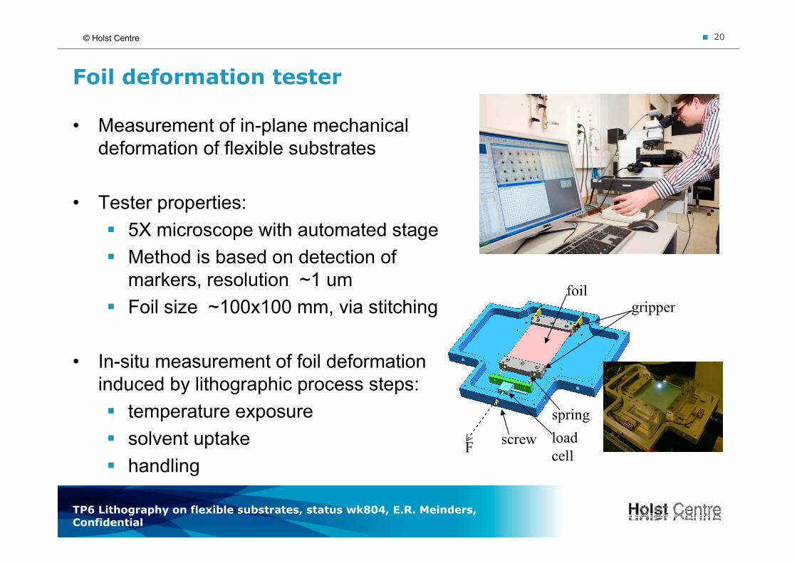
Foil deformation tester
• Measurement of in-plane mechanical
deformation of flexible substrates
• Tester properties:
� 5X microscope with automated stage
� Method is based on detection of
markers, resolution ~1 um
� Foil size ~100x100 mm, via stitching
• In-situ measurement of foil deformation
induced by lithographic process steps:
� temperature exposure
� solvent uptake
� handling
gripperfoil
spring
load
cellscrew
F
TP6 Lithography on flexible substrates, status wk804, E.R. Meinders, Confidential
� 21© Holst Centre
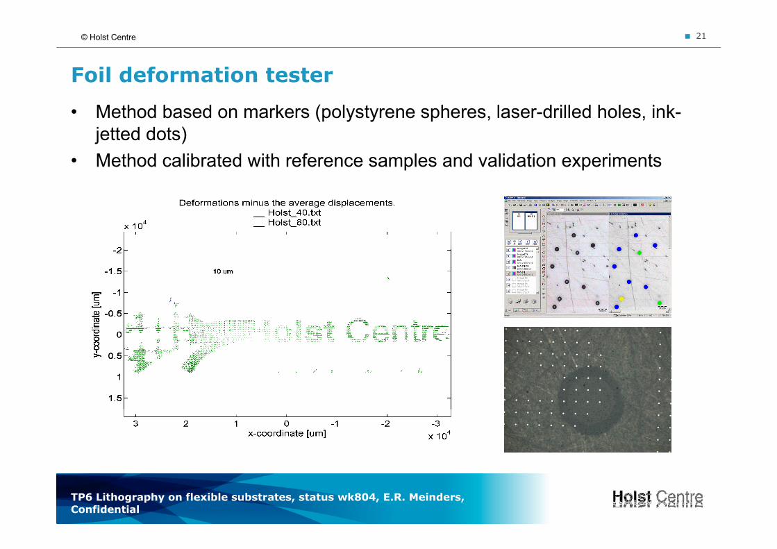
Foil deformation tester
• Method based on markers (polystyrene spheres, laser-drilled holes, ink-
jetted dots)
• Method calibrated with reference samples and validation experiments
TP6 Lithography on flexible substrates, status wk804, E.R. Meinders, Confidential
� 22© Holst Centre
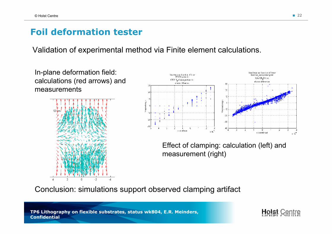
Validation of experimental method via Finite element calculations.
Conclusion: simulations support observed clamping artifact
In-plane deformation field:
calculations (red arrows) and
measurements
Effect of clamping: calculation (left) and
measurement (right)
Foil deformation tester
TP6 Lithography on flexible substrates, status wk804, E.R. Meinders, Confidential
� 23© Holst Centre
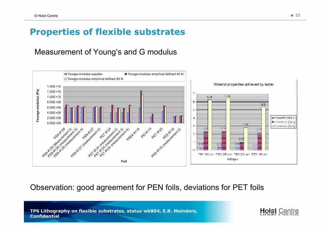
Measurement of Young’s and G modulus
0.00E+00
2.00E+09
4.00E+09
6.00E+09
8.00E+09
1.00E+10
1.20E+10
1.40E+10
PEN
#12
6
PEN
#12
6 (M
easu
remen
t 2)
PEN
#12
6 (m
easu
remen
t 3)
PEN
#12
6 (m
easu
remen
t 4)
PEN
#12
7
PEN
#12
7 (m
easu
remen
t 2)
PET
#12
4
PET
#12
4 (m
easu
remen
t 2)
PET
#12
4 (m
easu
remen
t 3)
PET
#12
4 (m
easu
remen
t 4)
PEE
K #
119
PEI
#11
3PET
#12
5PES
#11
6
PES
#11
6 (m
easu
remen
t 2)
Foil
Youngs-m
odulus (Pa)
Youngs-modulus supplier Youngs-modulus empirical defined 40 N
Youngs-modulus empirical defined 80 N
Observation: good agreement for PEN foils, deviations for PET foils
Properties of flexible substrates
TP6 Lithography on flexible substrates, status wk804, E.R. Meinders, Confidential
� 24© Holst Centre
FC_EF_026
M.D.
2.14 GPa
5.46 GPa
0.27
0.80·10-03
Position:
middle
T.D.External force
direction
2.36 GPaG-modulus
FC_EF_032Experiment nr.
6.13 GPaE-modulus
0.30Poisson’s ratio
0.70·10-03Strain (εy)
Position:
middle
PET foil, thickness: 100 um
Study of anisotropy PET foil
Observation: clear difference in mechanical behavior machine (MD) and
transverse direction (TD)
MD
MD
300 mm
TDTD
Properties of flexible substrates
TP6 Lithography on flexible substrates, status wk804, E.R. Meinders, Confidential
� 25© Holst Centre
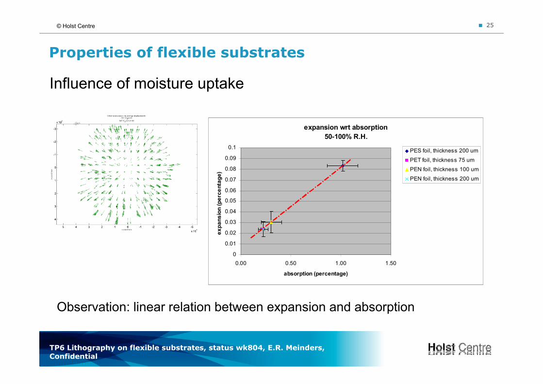
Influence of moisture uptake
Properties of flexible substrates
expansion wrt absorption
50-100% R.H.
0
0.01
0.02
0.03
0.04
0.05
0.06
0.07
0.08
0.09
0.1
0.00 0.50 1.00 1.50
absorption (percentage)
expansion (percentage)
PES foil, thickness 200 um
PET foil, thickness 75 um
PEN foil, thickness 100 um
PEN foil, thickness 200 um
Observation: linear relation between expansion and absorption
TP6 Lithography on flexible substrates, status wk804, E.R. Meinders, Confidential
� 26© Holst Centre
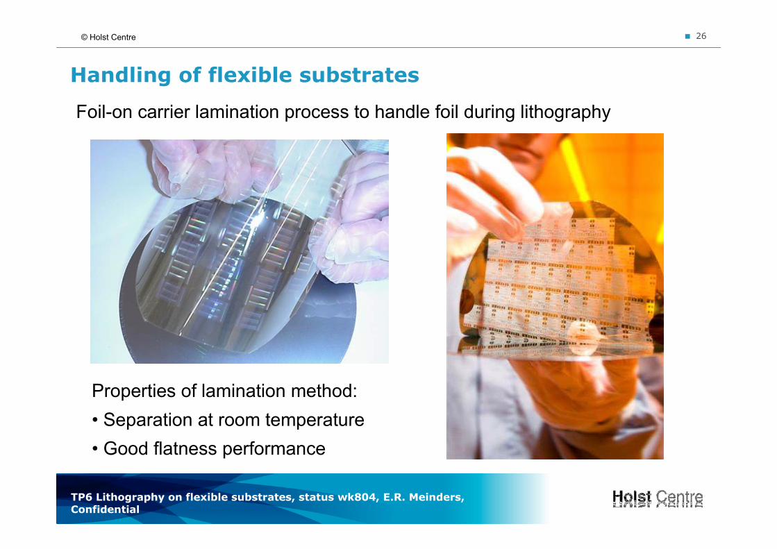
Handling of flexible substrates
Foil-on carrier lamination process to handle foil during lithography
Properties of lamination method:
• Separation at room temperature
• Good flatness performance
TP6 Lithography on flexible substrates, status wk804, E.R. Meinders, Confidential
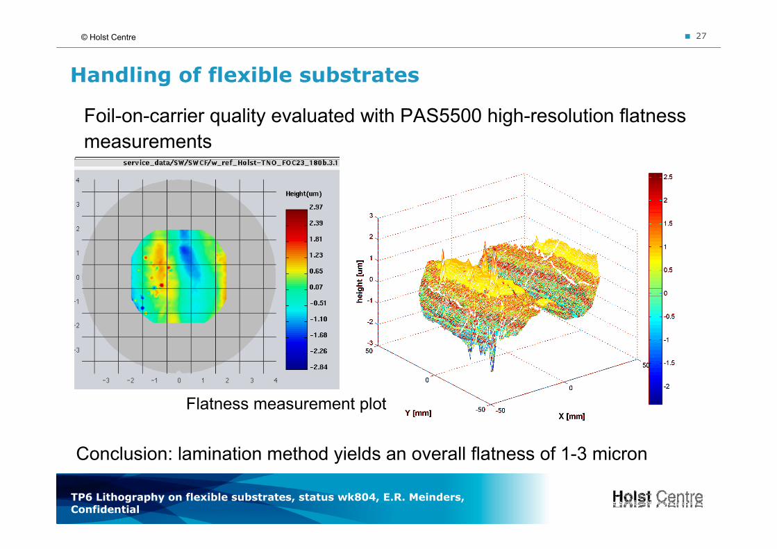
� 27© Holst Centre
Foil-on-carrier quality evaluated with PAS5500 high-resolution flatness
measurements
Flatness measurement plot
Conclusion: lamination method yields an overall flatness of 1-3 micron
Handling of flexible substrates
TP6 Lithography on flexible substrates, status wk804, E.R. Meinders, Confidential
� 28© Holst Centre
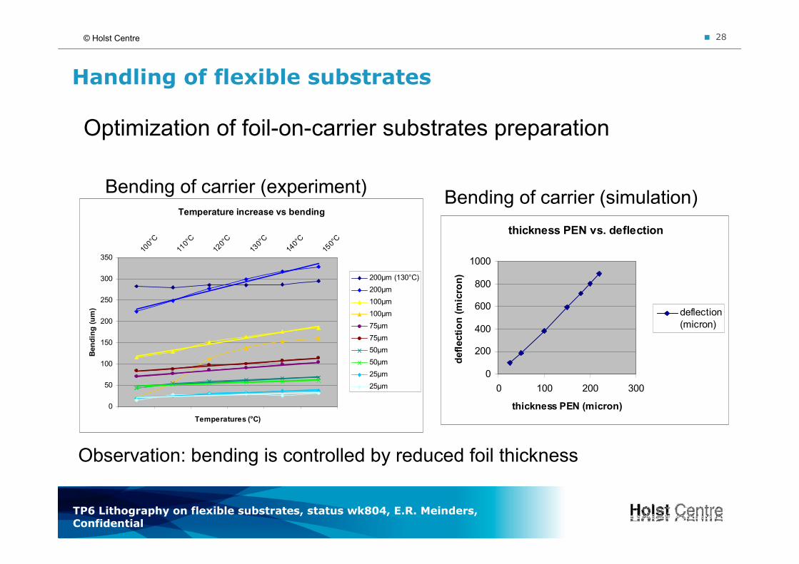
Optimization of foil-on-carrier substrates preparation
Temperature increase vs bending
0
50
100
150
200
250
300
350
100°
C
110°
C
120°
C
130°
C
140°
C
150°
C
Temperatures (°C)
Bending (um)
200µm (130°C)
200µm
100µm
100µm
75µm
75µm
50µm
50µm
25µm
25µm
Observation: bending is controlled by reduced foil thickness
thickness PEN vs. deflection
0
200
400
600
800
1000
0 100 200 300
thickness PEN (micron)
deflection (micron)
deflection
(micron)
Bending of carrier (experiment)
Handling of flexible substrates
Bending of carrier (simulation)
TP6 Lithography on flexible substrates, status wk804, E.R. Meinders, Confidential
� 29© Holst Centre
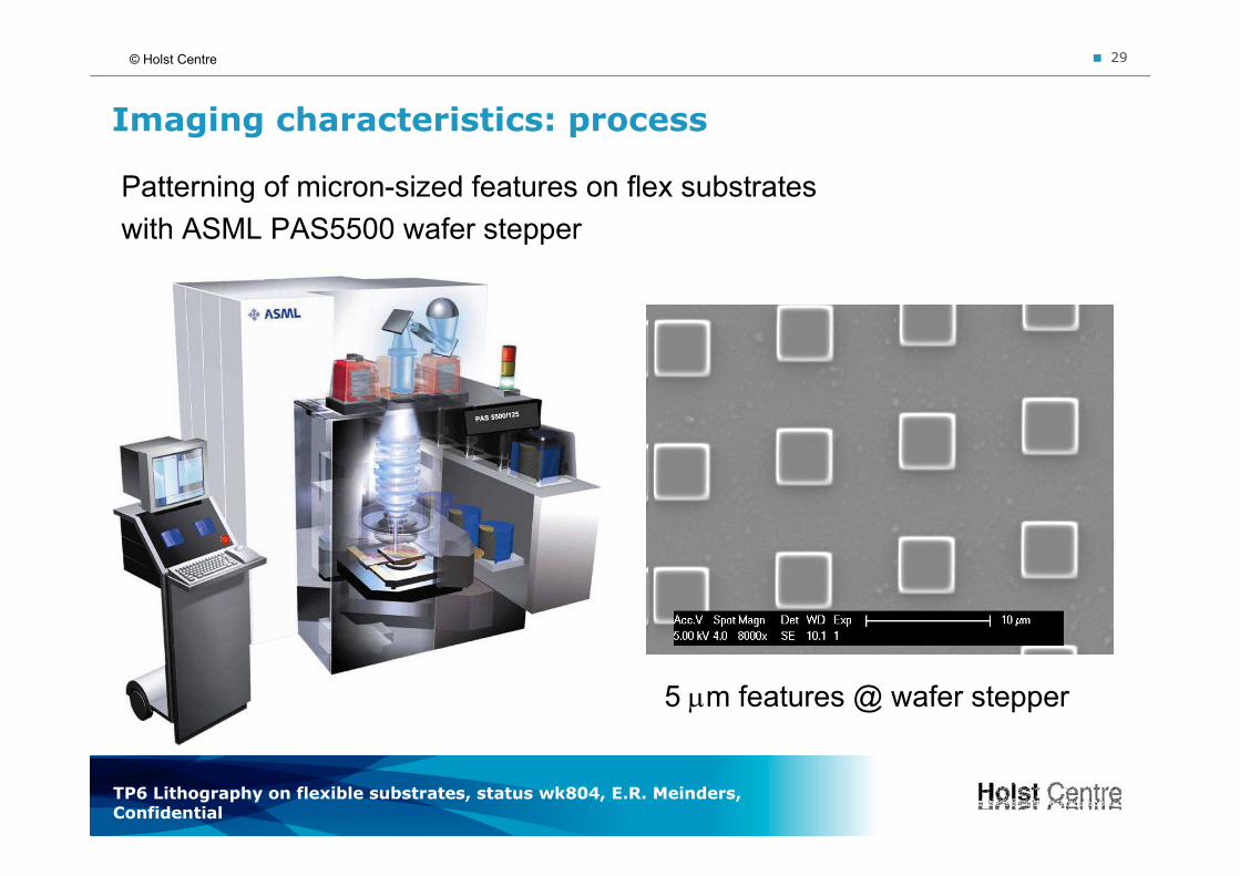
Patterning of micron-sized features on flex substrates
with ASML PAS5500 wafer stepper
Imaging characteristics: process
5 µm features @ wafer stepper
TP6 Lithography on flexible substrates, status wk804, E.R. Meinders, Confidential
� 30© Holst Centre
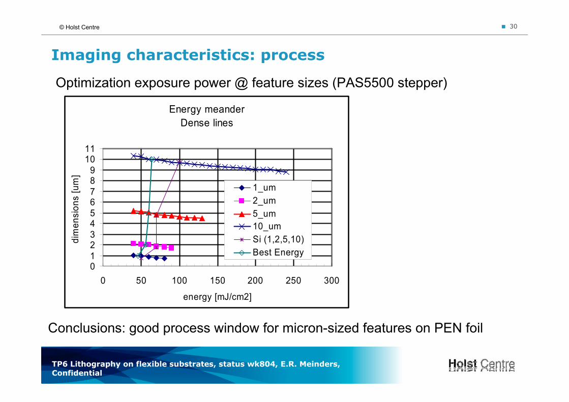
Optimization exposure power @ feature sizes (PAS5500 stepper)
Conclusions: good process window for micron-sized features on PEN foil
Imaging characteristics: process
Energy meander
Dense lines
01234567891011
0 50 100 150 200 250 300
energy [mJ/cm2]
dimensions [um]
1_um
2_um
5_um
10_um
Si (1,2,5,10)
Best Energy
TP6 Lithography on flexible substrates, status wk804, E.R. Meinders, Confidential
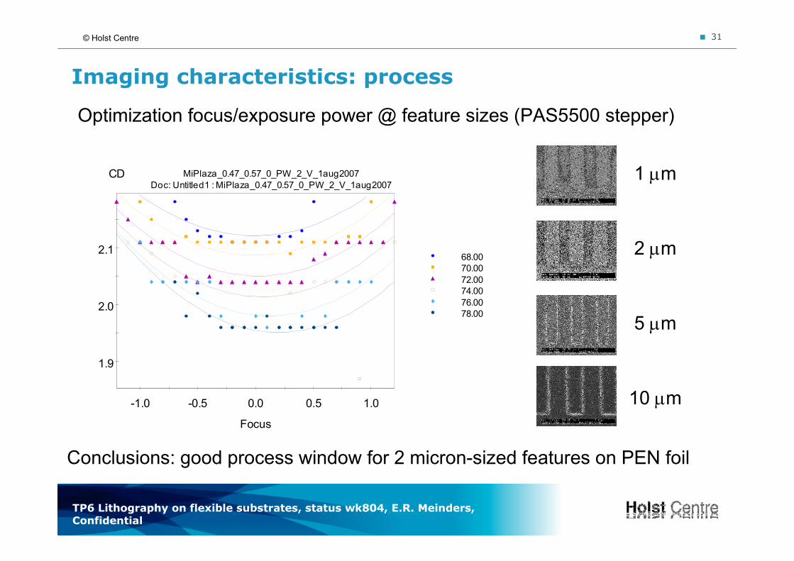
� 31© Holst Centre
1 µm
2 µm
5 µm
10 µm
Optimization focus/exposure power @ feature sizes (PAS5500 stepper)
Conclusions: good process window for 2 micron-sized features on PEN foil
Imaging characteristics: process
1.9
2.0
2.1
-1.0 -0.5 0.0 0.5 1.0
CD
Focus
68.00
70.00
72.00
74.00
76.00
78.00
MiPlaza_0.47_0.57_0_PW_2_V_1aug2007
Doc: Untitled1 : MiPlaza_0.47_0.57_0_PW_2_V_1aug2007
TP6 Lithography on flexible substrates, status wk804, E.R. Meinders, Confidential
� 32© Holst Centre
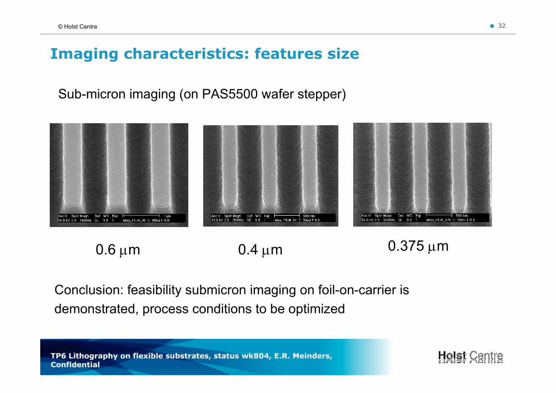
0.6 µm 0.4 µm 0.375 µm
Sub-micron imaging (on PAS5500 wafer stepper)
Conclusion: feasibility submicron imaging on foil-on-carrier is
demonstrated, process conditions to be optimized
Imaging characteristics: features size
TP6 Lithography on flexible substrates, status wk804, E.R. Meinders, Confidential
� 33© Holst Centre
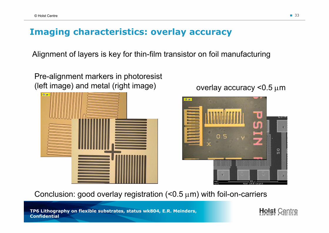
Alignment of layers is key for thin-film transistor on foil manufacturing
Conclusion: good overlay registration (<0.5 µm) with foil-on-carriers
Imaging characteristics: overlay accuracy
Pre-alignment markers in photoresist
(left image) and metal (right image) overlay accuracy <0.5 µm
TP6 Lithography on flexible substrates, status wk804, E.R. Meinders, Confidential
� 34© Holst Centre
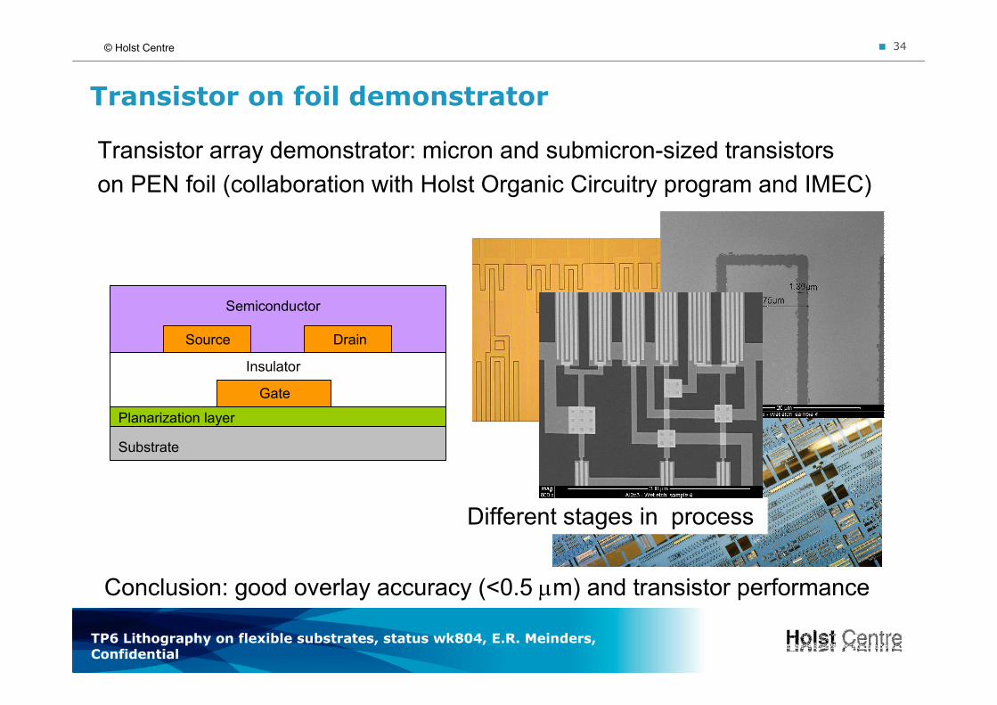
Transistor on foil demonstrator
Transistor array demonstrator: micron and submicron-sized transistors
on PEN foil (collaboration with Holst Organic Circuitry program and IMEC)
Conclusion: good overlay accuracy (<0.5 µm) and transistor performance
Different stages in process
Source Drain
Semiconductor
Insulator
Gate
Planarization layer
Substrate
Source Drain
Semiconductor
Insulator
Gate
Planarization layer
Substrate
TP6 Lithography on flexible substrates, status wk804, E.R. Meinders, Confidential
� 35© Holst Centre
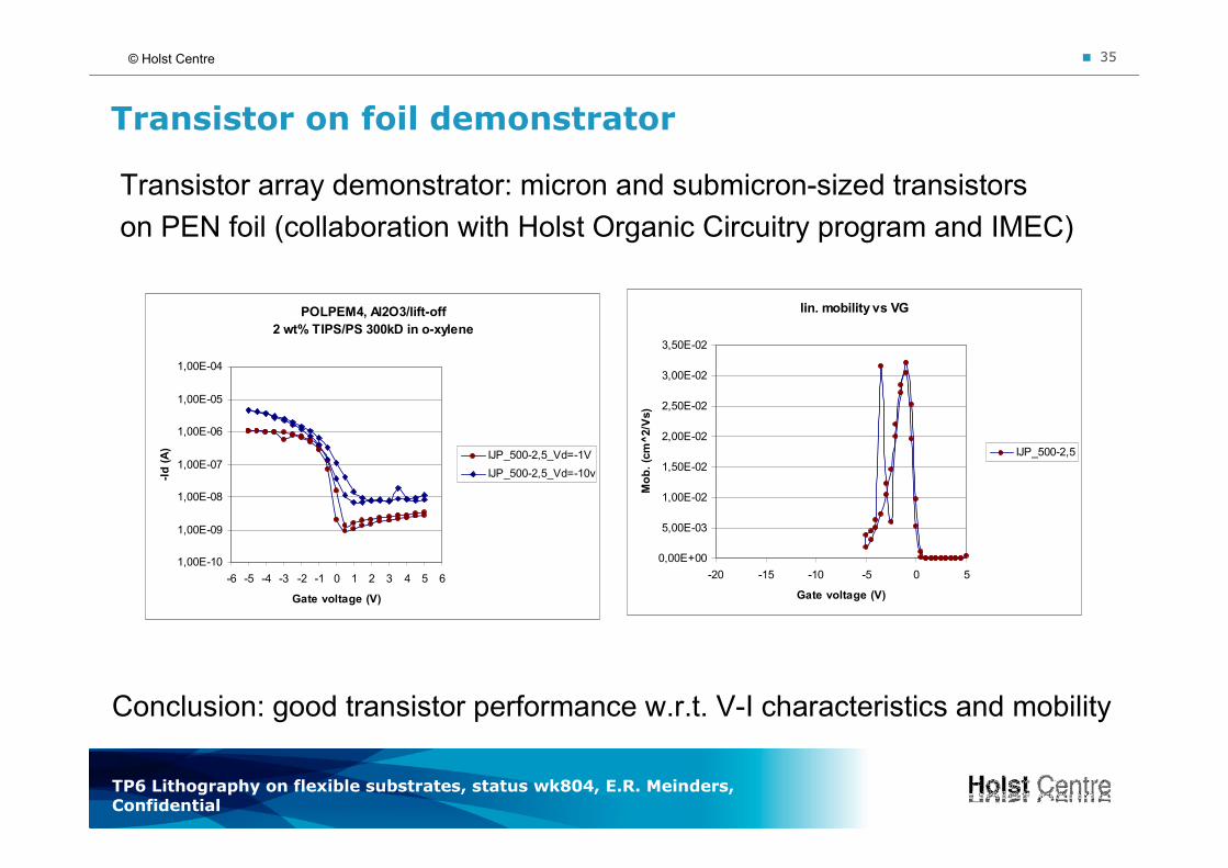
Transistor on foil demonstrator
Transistor array demonstrator: micron and submicron-sized transistors
on PEN foil (collaboration with Holst Organic Circuitry program and IMEC)
Conclusion: good transistor performance w.r.t. V-I characteristics and mobility
POLPEM4, Al2O3/lift-off
2 wt% TIPS/PS 300kD in o-xylene
1,00E-10
1,00E-09
1,00E-08
1,00E-07
1,00E-06
1,00E-05
1,00E-04
-6 -5 -4 -3 -2 -1 0 1 2 3 4 5 6
Gate voltage (V)
-Id (A)
IJP_500-2,5_Vd=-1V
IJP_500-2,5_Vd=-10v
lin. mobility vs VG
0,00E+00
5,00E-03
1,00E-02
1,50E-02
2,00E-02
2,50E-02
3,00E-02
3,50E-02
-20 -15 -10 -5 0 5
Gate voltage (V)
Mob. (cm^2/Vs)
IJP_500-2,5
January 29, 2008
Conclusions
Status technology program ‘Lithography on flexible substrates’
Erwin R. Meinders, Eindhoven, February 2008
TP6 Lithography on flexible substrates, status wk804, E.R. Meinders, Confidential
� 37© Holst Centre
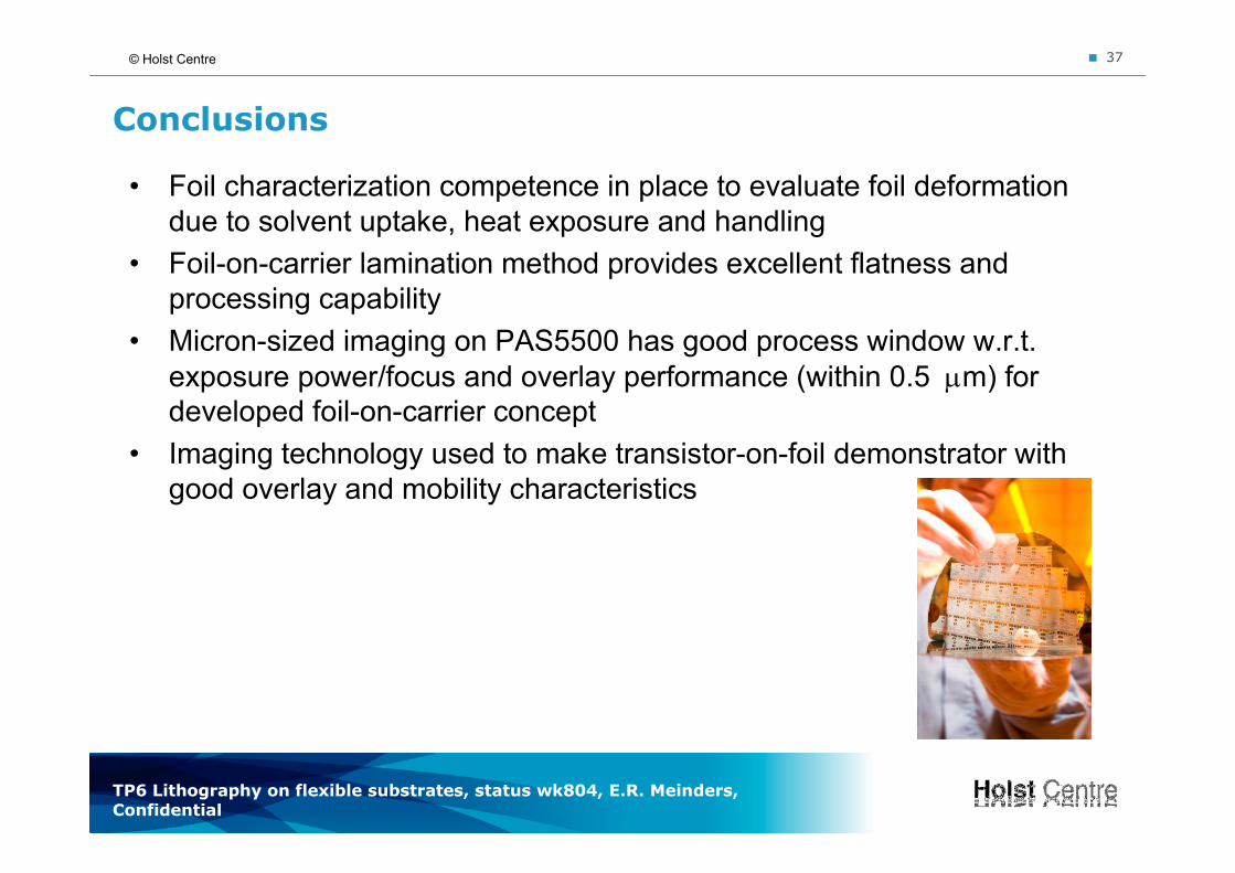
Conclusions
• Foil characterization competence in place to evaluate foil deformation
due to solvent uptake, heat exposure and handling
• Foil-on-carrier lamination method provides excellent flatness and
processing capability
• Micron-sized imaging on PAS5500 has good process window w.r.t.
exposure power/focus and overlay performance (within 0.5 µm) for
developed foil-on-carrier concept
• Imaging technology used to make transistor-on-foil demonstrator with
good overlay and mobility characteristics
January 29, 2008
program partners
Thanks for your attention. Questions?
Team members:
Wim de Laat (ASML)
Cheng Gui (ASML)
Peter Giesen
Iryna Yakimets
Maria Peter
Marius Ivan
François Furthner
Marloes Goorhuis
Bas van der Putten
Tom Geuns