channel link i design guide - ti.com · june 2006 national semiconductor channel link design guide...
TRANSCRIPT

DS90CR215,DS90CR216A,DS90CR217,DS90CR218A,DS90CR285,DS90CR286A,DS90CR287,DS90CR288A,DS90CR481,DS90CR482,DS90CR483A,DS90CR484A,DS90CR485,DS90CR486
Literature Number: SNLA167
June 2006
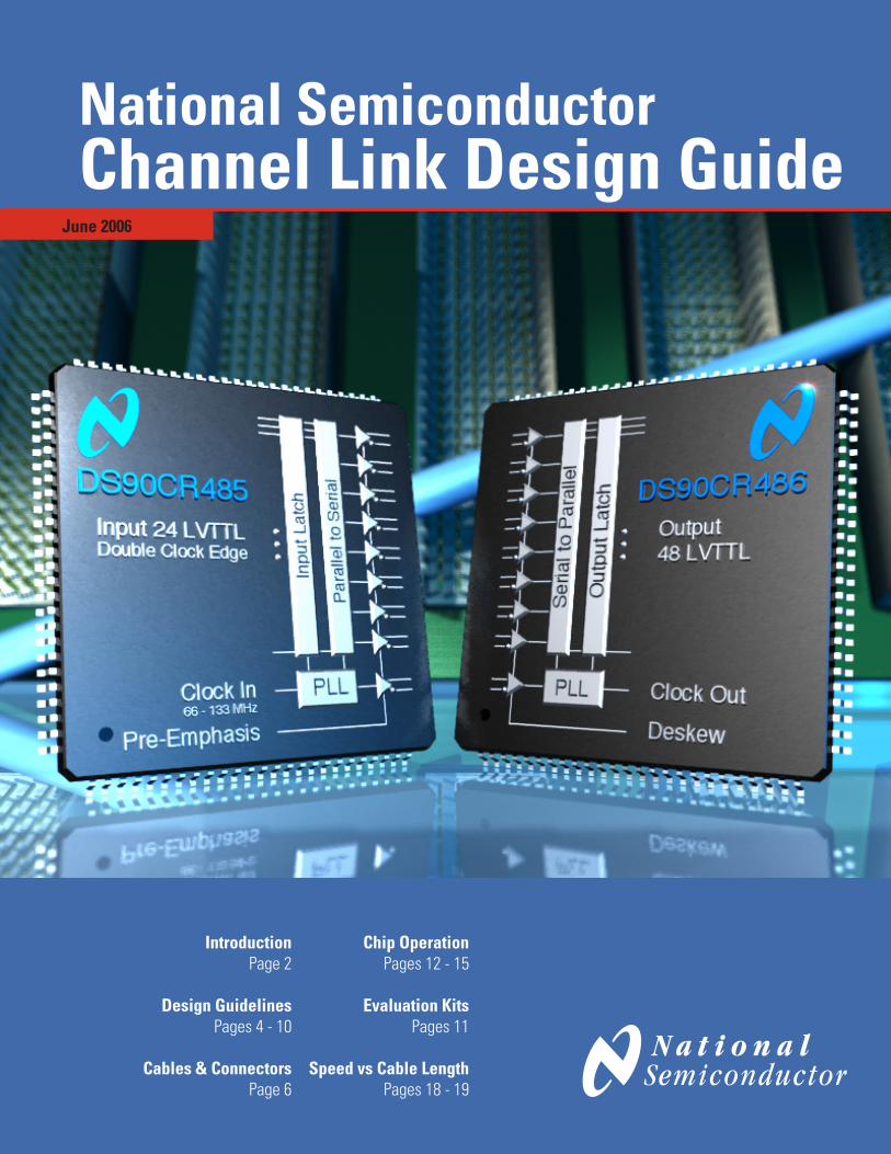
National SemiconductorChannel Link Design Guide
IntroductionPage 2
Design GuidelinesPages 4 - 10
Cables & ConnectorsPage 6
Chip OperationPages 12 - 15
Evaluation KitsPages 11
Speed vs Cable LengthPages 18 - 19
2
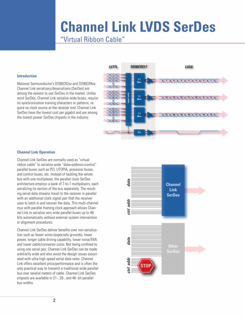
Channel Link LVDS SerDes“Virtual Ribbon Cable”
Introduction
National Semiconductor’s DS90CR2xx and DS90CR4xx Channel Link serializers/deserializers (SerDes) are among the easiest to use SerDes in the market. Unlike most SerDes, Channel Link serialize wide buses, require no synchronization training characters or patterns, re-quire no clock source at the receiver end. Channel Link SerDes have the lowest cost per gigabit and are among the lowest power SerDes chipsets in the industry.
Channel Link Operation
Channel Link SerDes are normally used as “virtual ribbon cable” to serialize wide “data+address+control” parallel buses such as PCI, UTOPIA, processor buses, and control buses, etc. Instead of tackling the whole bus with one multiplexer, the parallel clock SerDes architecture employs a bank of 7-to-1 multiplexers, each serializing its section of the bus separately. The result-ing serial data streams travel to the receiver in parallel with an additional clock signal pair that the receiver uses to latch in and recover the data. This multi-channel mux with parallel framing clock approach allows Chan-nel Link to serialize very wide parallel buses up to 48 bits automatically without external system intervention or alignment procedures.
Channel Link SerDes deliver benefits over non-serializa-tion such as fewer wires (especially grounds), lower power, longer cable driving capability, lower noise/EMI, and lower cable/connector costs. Not being confined to using one serial pair, Channel Link SerDes can be made arbitrarily wide and also avoid the design issues associ-ated with ultra high speed serial data rates. Channel Link offers excellent price/performance and is often the only practical way to transmit a traditional wide parallel bus over several meters of cable. Channel Link SerDes chipsets are available in 21-, 28-, and 48- bit parallel bus widths.

Channel Link Products Selection Guide
Channel Link LVDS Serializers & Deserializers
Features
• Wide 21-, 28-, and 48- bit bus widths
• Raw data payloads up to 6.38 Gbps
• Automatic receiver lock without training patterns or characters, “Plug & Go”
• No external coding or framing required
• Very low power consumption
• Wide operating frequency, relaxed transmit clock requirements
• Deserializer requires no external clock source
• Lowest cost per gigabit
• Easy to use over cables and FR-4 backplanes
• Extended temperature ranges
• 3.3V and 5V chipset interoperability
• Standard TSSOP & TQFP packaging
Which 48-bit Chipset Should I Use?
Clock Frequency Recommended Chipset
< 66 MHz DS90CR483/484
66 - 112 MHz DS90CR481/482, DS90CR481/486†, or
DS90CR485/6
> 112 MHz DS90CR485/486
† For long cables (e.g. over 8 m) at ≥ 66 MHz, the DS90CR481/486 combination is recommended.
Part Number MuxRatio
Function Bus Speed (MHz)
Through-put (Gbps)
Supply Voltage
Temperature Package Eval Kit
21-bit
DS90CR213MTD 21:3 Transmitter 20 - 66 1.38 5 -10 to +70°C TSSOP-48 See Note 1
DS90CR214MTD 21:3 Receiver 20 - 66 1.38 5 -10 to +70°C TSSOP-48 See Note 1
DS90CR215MTD 21:3 Transmitter 20 - 66 1.38 3.3 -40 to +85°C TSSOP-48 See Note 1
DS90CR216AMTD 21:3 Receiver 20 - 66 1.38 3.3 -40 to +85°C TSSOP-48 See Note 1
DS90CR217MTD 21:3 Transmitter 20 - 85 1.78 3.3 -10 to +70°C TSSOP-48 See Note 1
DS90CR218AMTD 21:3 Receiver 20 - 85 1.78 3.3 -10 to +70°C TSSOP-48 See Note 1
28-bit
DS90CR283MTD 28:4 Transmitter 20 - 66 1.84 5 -10 to +70°C TSSOP-56 See Note 1
DS90CR284MTD 28:4 Receiver 20 - 66 1.84 5 -10 to +70°C TSSOP-56 See Note 1
DS90CR285MTD 28:4 Transmitter 20 - 66 1.84 3.3 -40 to +85°C TSSOP-56 See Note 1
DS90CR286AMTD 28:4 Receiver 20 - 66 1.84 3.3 -40 to +85°C TSSOP-56 See Note 1
DS90CR287MTD 28:4 Transmitter 20 - 85 2.38 3.3 -10 to +70°C TSSOP-56 CLINK3V28BT-85
DS90CR288AMTD 28:4 Receiver 20 - 85 2.38 3.3 -10 to +70°C TSSOP-56 CLINK3V28BT-85
48-bit
DS90CR481VJD 48:8 Transmitter 65 - 112 5.37 3.3 -10 to +70°C TQFP-100 CLINK3V48BT-112
DS90CR482VS 2 48:8 Receiver 65 - 112 5.37 3.3 -10 to +70°C TQFP-100 CLINK3V48BT-112
DS90CR483VJD 48:8 Transmitter 33 - 112 5.37 3.3 -10 to +70°C TQFP-100 CLINK3V48BT-112
DS90CR484VJD 48:8 Receiver 33 - 112 5.37 3.3 -10 to +70°C TQFP-100 CLINK3V48BT-112
DS90CR485VS 2 48:8 Transmitter 66 - 133 6.38 2.5/3.3 -10 to +70°C TQFP-100 CLINK3V48BT-133
DS90CR486VS 2 48:8 Receiver 66 - 133 6.38 3.3 -10 to +70°C TQFP-100 CLINK3V48BT-133 1 Use 85 MHz 28-bit evaluation kit for proof of concept. This evaluation kit can be reworked to accept non-85 MHz, non-28-bit devices if necessary.2 Package codes: National has recently moved to 2-letter package code suffixes for new products. Therefore, the new VS code refers to the same TQFP-100 pack-age as the old VJD code.
4
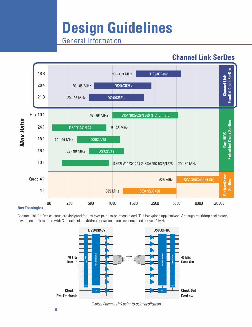
Design GuidelinesGeneral Information
Bus Topologies
Channel Link SerDes chipsets are designed for use over point-to-point cable and FR-4 backplane applications. Although multidrop backplanes have been implemented with Channel Link, multidrop operation is not recommended above 40 MHz.
Bus
LVD
SEm
bedd
ed C
lock
Ser
Des
Chan
nel L
ink
Para
llel C
lock
Ser
Des
Bit
Inte
rlea
veSe
rDes
100
4:1
Quad 4:1
10:1 20 - 80 MHz
16:1
18:1
21:3
28:4
48:8
Hex 10:1
625 MHz
625 MHz
10:1
25 - 80 MHz
15 - 66 MHz
20 - 85 MHz
20 - 85 MHz
33 - 133 MHz
16 - 66 MHz
250 500 1000 1500
Data Payload (Mbps)
Mux
Rat
io
2500 5000 10000 20000
SCAN50C400
DS92LV1023/1224 & SCAN921025/1226
DS92LV16
DS92LV18
24:1 5 - 35 MHzDS90C241/124
DS90CR21x
DS90CR28x
DS90CR48x
SCAN928028/6260 (6 Channels)
SCAN50C400 (4 Ch)
Channel Link SerDes
Typical Channel Link point-to-point application

PCB Recommendations
General Printed Circuit Board (PCB) Recommen-dations
• Use at least 4 PCB board layers (LVDS signals, ground, power, and TTL signals).
• Minimize pair-to-pair skew between LVDS clock and data
• Use proper power supply bypassing such that PLL VCC noise is less than 100 mV peak-to-peak.
• Controlled impedance differential traces of 100 Ohms are recommended for LVDS signals. Edge-coupled microstrip, edge-coupled stripline, or broadside-coupled stripline differential traces may be used. These traces should be closely-coupled (i.e. “s” should be minimized) to ensure coupled noise will appear as common-mode (which is rejected by the receiver). This has the added benefit that closely-coupled lines that are excited with odd-mode transmission tend to radiate less electromag-netic energy.
• Treat the entire LVDS clock+data bus as one signal, avoiding influences that cause imbalances within the pair (see diagram at right). Minimize skew within the pair. Maintain “balance.”
• Tie unused TTL inputs high or low. Leave unused LVDS deserializer inputs open (floating) – internal failsafe will pull the input to a valid state.
• Termination of the LVDS signals is required. The termination resistor value should match the differential impedance of the transmission line. 100-Ohm is a typi-cal value for point-to-point applications. It is better err with too large a termination resistor than too small.
• Isolate TTL/CMOS signals from LVDS signals, placing them at least “3s” or “2w” away—whichever is larger. This will help to prevent them from coupling onto the LVDS lines.
These are just a few common practices that should be followed when designing PCBs for LVDS signaling. General application guidelines are available in the LVDS Owner’s Manual and other documents at lvds.national.com.

6
Design GuidelinesCables & Connectors
Cables
Channel Link SerDes can be used over a wide variety of balanced, 100-Ohm differen-tial cables depending on distance and signal quality requirements. In general, twinax or shielded twisted pair cables are recommended. Low pair-to-pair skew is the most important parameter to consider when choosing a cable assembly for Channel Link.
• SCSI-type cables and connectors or LVDS-type cable assemblies such as the 3M™ MDR and Amphenol SKEWCLEAR® systems are commonly used. See the “Data Rate vs. Cable Length” section for typical performance using 3M MDR cable assemblies.
• Other high performance shielded multi-pair cables such as Infiniband/CX4 assem-blies may be used.
• Very Short Distances (< 0.3 m): flex circuit (following correct PCB layout) or unbal-anced ribbon cable may be used. Use ground conductors between LVDS pairs and avoid using end conductors for LVDS signals.
At least one ground conductor should be used in the cable to provide a known, low impedance return path for common mode currents.
A termination resistor RL, placed as close as possible to the receiver inputs in point-to-point applications, is required. The resistor value should be chosen to match the differential impedance of the cable.
Connectors
SCSI-type connectors like 3M MDR and CHAMP connectors are typically used. Connectors with differential conductors offer the highest performance, but are not necessary in low speed or short distance applications. For single-ended connectors, keep LVDS pins away from other signals, particularly TTL/CMOS/LVTTL/LVCMOS sig-nals. The “+” and “-” signals of a pair should be routed on the same row in multi-row backplane connectors to help minimize skew within the pair.
Twinax cable construction
Unshielded twisted pair (UTP) cable construction
Connector pin assignment for low skew.Top-good; bottom-bad.
3M MDR Cable System

Power & Ground
General Power/Ground Recommendations
A solid power/ground system is the foundation on which a reliable interconnect system is built. Design circuit board layout and stack-up for the system to provide noise-free power to the device. Good layout practice will separate high frequency and high level inputs and outputs to minimize unwanted stray noise pickup, feedback, and interfer-ence. Power system performance may be greatly improved by using thin dielectrics (4 to 10 mils) for power/ground sandwiches. This increases the intrinsic capacitance of the PCB power system, which improves power supply filter-ing—especially at high frequencies—making the value and placement of external bypass capacitors less critical. External bypass capacitors should include both RF ceramic and tantalum electrolytic types. Use RF capacitors in the range of 0.001 µF to 0.1 µF. Use tantalum capacitors in the range of 2.2 µF to 10 µF. The voltage rating of tantalum capacitors should be at least 3 (5 preferred) times the power supply voltage being used.
It is recommended practice to use two vias at each power/ground pin as well as all RF bypass capacitor terminals. Dual vias reduce the interconnect inductance by up to half, thereby extending the effective range of bypass compo-nents. Locate RF capacitors as close as possible to the supply pins and use wide, low impedance traces—not 50-Ohm traces. Surface mount capacitors are recommended due to lower parasitics. When using multiple capacitors per supply pin, locate the smallest value closest to the supply pin. A bulk capacitor is recommended at the point of power entry. This is typically in the range of 50 µF to 100 µF and will smooth low frequency noise.
Some devices have separate power/ground pins for different portions of the circuits to isolate switching noise effects between different blocks. Connecting these to separate power/ground planes on the PCB is typically not required. Pin description tables typically describe which blocks are connected to which power/ground pins. In some cases, an external filter may be used to provide clean power to sensitive circuits such as PLLs.
Channel Link Recommendations
General device-specific bypassing recommendations are given below. Actual best practice depends on other board and system level criteria in-cluding board density, power rail and power supply type, and the supply needs of other integrated circuits on the board. When minimizing supply noise, priority should be given in this order: PLL, LVDS, and then digital VCC pins.
PLL Supply
The PLL VCC pins supply the PLL circuits. PLLs require a clean supply—less than 100 mV noise peak-to-peak—for the minimization of jitter and best link margin. PLL VCC noise in the frequency range 200 kHZ to 3 MHz can increase jitter and reduce noise margins. Certain power supplies may have switching frequencies or high harmonic content in this range. If this is the case, filtering of this noise spectrum may be required. A notch filter response is best to provide stable VCC, suppression of the noise band, and good high frequency response (clock fundamental). This may be accomplished with a CRC or CLC pie filter. If employed, a separate pie filter is recommended for each PLL to minimize the voltage drop due to series resistance. Separate board power planes for each PLL VCC pin is not required.
LVDS Supply
The LVDS VCC pins supply the LVDS circuits. Due to the nature of the Channel Link, large currents are not drawn through these pins and a 0.1 µF capacitor is normally sufficient for these pins. If space is available, a 0.01 µF capacitor may be used in parallel with the 0.1 µF capacitor for addi-tional high frequency filtering. Connect the LVDS ground to the cable ground to provide a return path for any common (even) mode currents. Most of the LVDS current is odd-mode and returns within the pair, though a small amount of odd-mode current may be present due to coupled noise and the cable ground should return through a low impedance path to LVDS ground pins.
Digital Supply
The digital VCC pins supply the digital portion of the device and also the receiver TTL output drivers. The receiver digital VCC is more critical than the transmitter digital VCC because it must power the receiver outputs during multiple output switching conditions. Bypassing for receiver digital Vcc can be estimated as follows:
Total digital bypassing capacitance = (number TTL receiver outputs/digital VCC pins) x (max short circuit current x output rise time) ÷ (max allowed VCC droop, typically 50 mV)
50 Ω

8
Design GuidelinesInputs & Outputs
LVDS Termination
LVDS termination is required. Choose the termination resistor value RL to match the loaded differential impedance of the transmission line. In point-to-point applications, the termination value is typically 100 Ohms. Place a termination resistors as close as possible to the receiver inputs or end of the transmission lines.
Input Over- and Undershoot
Excessive over- and undershoot injects noise into the power supply and PLL, decreasing link margin. Reduce FPGA output drive to ensure over- and undershoot are minimized and < 300 mV above and below power/ground. Terminate LVTTL lines if necessary.
Transmitter Input Clock Jitter (TxCLKIN)
For Channel Link SerDes, cycle-to-cycle jitter is more critical than long term jitter. Although Channel Link SerDes employ jitter filters and have been characterized with cycle-to-cycle input clock impulses up to ± 300 ps, cycle-to-cycle input clock jitter should be minimized so that the serial-izer LVDS clock cycle-to-cycle jitter is less than 100 ps.
Spread Spectrum Clocking
Spread spectrum clocking can be used with Channel Link SerDes. Down spectrum is preferred over center or up spectrum since this increases tim-ing margins. Spread spectrum of 1-2% with a carrier frequency < 200 kHz (50 - 100 kHz is common) is recommended to ensure the PLL tracking.
Receiver Output Clock (RxCLKOUT)
The receiver output clock is an LVCMOS output whose rising edge is aligned to the middle of the receiver output data RxOUT. The subsequent ASIC/FPGA device should latch in RxOUT data meeting the ASIC/FPGAs input setup and hold times. Output jitter for RxCLKOUT is not specified on the datasheet since it depends on the jitter of the incoming data and the TxCLKIN clock source.
Interoperability of Channel Link Chipsets
Any 21-bit Channel Link serializer can be used with any 21-bit Channel Link deserializer over the devices’ overlapping operating frequency ranges. The same is true for 28- and 48- bit chipsets. The power supplies of the serializer and deserializer do not need to be the same, in fact, 5V and 3.3V Channel Link serializers and deserializers may be used on different ends of the link.
Unused TTL Inputs
Unused LVTTL inputs should be tied high or low. Many Channel Link devices (check devices) have internal pull down devices to bias unused pins. These internal impedances tend to be in the 200 kOhm range and may be overridden with lower value pull up resistors if desired.
Floating LVDS Receiver Inputs & Failsafe
In the event that the Channel Link receiver is disconnected from the backplane/cable, the internal failsafe circuitry is designed to reject a certain amount of differential noise (about 10 mV) from being interpreted as data or clock. This seems like a very small threshold, but balanced, closely-coupled LVDS lines tend to pick up noise as common mode—not differential. Additional failsafe biasing can be implemented externally (see application note AN-1194 and LVDS Owner’s Manual sections 4.6.2-3) at the expense of two additional resistors. Receiver data and clock output status when its LVDS inputs are floating is shown in the table at the end of this design guide.
Receiver Output Drive
To minimize EMI and power consumption, Channel Link receiver output drive is on the order of a few milliamps. This is typically sufficient to drive 1-2 LVTTL/LVCMOS loads. If more loads or long traces will be driven, especially at higher clock speeds, a logic buffer is recommended. Note that depending on actual configuration (number of loads, stub lengths, segment distances, etc.), the receiver output bus may need to be treated as a transmission line and proper LVTTL/LVCMOS termination techniques employed.
Probing Signals & App Notes
Probing LVDS Signals
LVDS signals are high speed, low swing signals. Improper probing can result in deceiving results since the probe and/or scope can filter high speed components of the signal. Using a >1 GHz bandwidth scope (such as the Agilent 86100 or Tektronix 694C) and a high speed differential probe (such as the Tektronix P6247/8 or P6330) is highly recommended. LVDS drivers are not compatible with 50-Ohm probes.
Related Application Material at www.national.com
Number Description
— LVDS Owner’s Manual, 3rd Edition
AN-905 Transmission Line RAPIDESIGNER Operation and Applications Guide
AN-971 Introduction to LVDS
AN-1041 Introduction to Channel Link
AN-1059 Timing (RSKM) Information
AN-1084 Parallel Application of Link Chips
AN-1108 PCB and Interconnect Design Guidelines
AN-1109 Multi-drop Application of Channel Links
AN-1194 Failsafe Biasing of LVDS Interfaces
White Paper
SerDes Architectures and Applications (available at LVDS.national.com)

10
Ω
Design Tip Overview
Channel Link are robust, easy-to-use SerDes, but to get the best performance from your interconnect design, it’s a good idea to review your design for best practices.
• Pair-to-Pair Skew: Large skew between LVDS clock and data pairs can cause mis-sampling of data. Make sure pair-to-pair skew meets RSKM requirements.
• Power Supply Noise: Excessive supply noise, especially on the PLL supply, can add jitter to the transmitter serial output and affect the receiver data sampling. Keep supply noise under 100 mV peak-to-peak on PLL VCC pins.
• Transmit Clock: Minimize excessive cycle-to-cycle jitter on the transmit clock TxCLKIN in the range of 200 kHz - 3 MHz which can add jitter to the transmitter serial output.
• Serial Bus: Should follow LVDS PCB layout and backplane recommendations, using proper termination, avoiding long stubs, and assuring the termination resistor is close to the receiver input.
• Parallel Bus: The parallel TTL signals should meet setup and hold times and should be free from excessive overshoot/undershoot. Buffer receiver TTL outputs RxOUT if driving long PCB traces and/or more than 1-2 loads.
Design ReviewCheck Your Design for High Performance

11
Evaluation BoardsCLINK3V28BT-85, CLINK3V48BT-112, CLINK3V48BT-133
Part Number Evaluation Kit
21-bit
DS90CR213 Use CLINK3V28BT-85. Replace the DS90CR287 with the DS90CR283. Pull TxIN[21:27] high or low. Con-nect to 5V supply.
DS90CR214 Use CLINK3V28BT-85. Replace the DS90CR288A with the DS90CR284. Pull TxIN[21:27] high or low. Con-nect to 5V supply.
DS90CR215 Use CLINK3V28BT-85. Replace the DS90CR287 with the DS90CR285. Pull TxIN[21:27] high or low.
DS90CR216/A Use CLINK3V28BT-85. Replace the DS90CR288A with the DS90CR286A. Pull TxIN[21:27] high or low.
DS90CR217 Use CLINK3V28BT-85. Pull TxIN[21:27] high or low.
DS90CR218/A Use CLINK3V28BT-85. Pull TxIN[21:27] high or low.
28-bit
DS90CR283 Use CLINK3V28BT-85. Replace the DS90CR287 with the DS90CR283. Connect to 5V supply.
DS90CR284 Use CLINK3V28BT-85. Replace the DS90CR288A with the DS90CR284. Connect to 5V supply.
DS90CR285 Use CLINK3V28BT-85. Replace the DS90CR287 with the DS90CR285.
DS90CR286/A Use CLINK3V28BT-85. Replace the DS90CR288A with the DS90CR286A.
DS90CR287 CLINK3V28BT-85
DS90CR288/A CLINK3V28BT-85
48-bit
DS90CR481 CLINK3V48BT-112. Replace the DS90CR483 with the DS90CR481.
DS90CR482 CLINK3V48BT-112. Replace the DS90CR484 with the DS90CR482.
DS90CR483 CLINK3V48BT-112
DS90CR484 CLINK3V48BT-112
DS90CR485 CLINK3V48BT-133
DS90CR486 CLINK3V48BT-133
Evaluation Boards
Three Channel Link evaluation kits are available from National Semiconductor and its distributors. With just these three kits, any Channel Link SerDes chipset can be evalu-ated since 28- and 21- bit Channel Link chipsets are pin compatible (see table at right for more info). In addition, the kits are interoperable, e.g.. 5V transmitter boards can talk to 3V receiver boards, 21-bit transmitter boards can drive 28-bit boards, etc.
CLINKV28BT-8
CLINKV48BT-112
CLINKV48BT-1
12
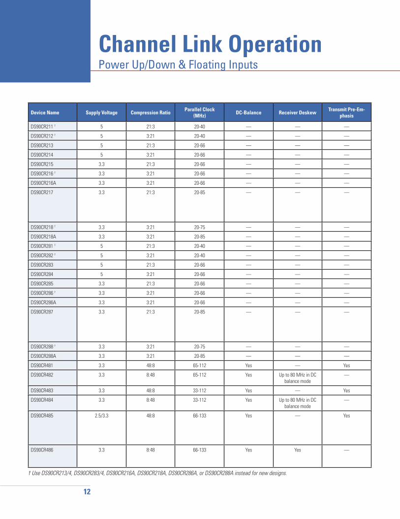
Channel Link OperationPower Up/Down & Floating Inputs
Device Name Supply Voltage Compression Ratio Parallel Clock (MHz) DC-Balance Receiver Deskew Transmit Pre-Em-
phasis
DS90CR211 † 5 21:3 20-40 — — —
DS90CR212 † 5 3:21 20-40 — — —
DS90CR213 5 21:3 20-66 — — —
DS90CR214 5 3:21 20-66 — — —
DS90CR215 3.3 21:3 20-66 — — —
DS90CR216 † 3.3 3:21 20-66 — — —
DS90CR216A 3.3 3:21 20-66 — — —
DS90CR217 3.3 21:3 20-85 — — —
DS90CR218 † 3.3 3:21 20-75 — — —
DS90CR218A 3.3 3:21 20-85 — — —
DS90CR281 † 5 21:3 20-40 — — —
DS90CR282 † 5 3:21 20-40 — — —
DS90CR283 5 21:3 20-66 — — —
DS90CR284 5 3:21 20-66 — — —
DS90CR285 3.3 21:3 20-66 — — —
DS90CR286 † 3.3 3:21 20-66 — — —
DS90CR286A 3.3 3:21 20-66 — — —
DS90CR287 3.3 21:3 20-85 — — —
DS90CR288 † 3.3 3:21 20-75 — — —
DS90CR288A 3.3 3:21 20-85 — — —
DS90CR481 3.3 48:8 65-112 Yes — Yes
DS90CR482 3.3 8:48 65-112 Yes Up to 80 MHz in DC balance mode
—
DS90CR483 3.3 48:8 33-112 Yes — Yes
DS90CR484 3.3 8:48 33-112 Yes Up to 80 MHz in DC balance mode
—
DS90CR485 2.5/3.3 48:8 66-133 Yes — Yes
DS90CR486 3.3 8:48 66-133 Yes Yes —
† Use DS90CR213/4, DS90CR283/4, DS90CR216A, DS90CR218A, DS90CR286A, or DS90CR288A instead for new designs.

1
Power Up/Down & Floating Inputs
Device NameAll Inputs Floating/Failsafe Power Down No Input Clock
Recommended Power-Up SequenceClock Outputs Data Outputs Clock Outputs Data Outputs Clock Outputs Data Outputs
DS90CR211 † High-Z High-Z High-Z High-Z Low Low —
DS90CR212 † High High High Prior State High Prior State —
DS90CR213 High-Z High-Z High-Z High-Z Low Low —
DS90CR214 High High High Prior State High Prior State —
DS90CR215 High-Z High-Z High-Z High-Z High-Z High-Z —
DS90CR216 † High High High Low High Low —
DS90CR216A High High High Low High Low —
DS90CR217 High-Z High-Z High-Z High-Z Active Low 1) Power up with /PD pin LOW 2) Bring /PD highor1) Apply clock2) Power up
DS90CR218 † High High Low Low Active Low —
DS90CR218A High High High Low Active Low —
DS90CR281 † High-Z High-Z High-Z High-Z Low Low —
DS90CR282 † High High High Prior State High Prior State —
DS90CR283 High-Z High-Z High-Z High-Z Low Low —
DS90CR284 High High High Prior State High Prior State —
DS90CR285 High-Z High-Z High-Z High-Z High-Z High-Z —
DS90CR286 † High High High Low High Low —
DS90CR286A High High High Low High Low —
DS90CR287 High-Z High-Z High-Z High-Z Active Low 1) Power up with /PD pin LOW 2) Bring /PD highor1) Apply clock2) Power up
DS90CR288 † High High Low Low Active Low —
DS90CR288A High High High Low Active Low —
DS90CR481 High-Z High-Z High-Z High-Z High-Z High-Z —
DS90CR482 High Low Low Low High Low —
DS90CR483 High-Z High-Z High-Z High-Z High-Z High-Z —
DS90CR484 High Low Low Low High Low —
DS90CR485 High-Z High-Z High-Z High-Z High-Z High-Z Power up both supplies togetheror1) Power up 3.3 V first, then 2.5 V supply2) Apply clock3) Bring /PD pin high
DS90CR486 Low High Low Low Low Prior State —
† Use DS90CR213/4, DS90CR283/4, DS90CR216A, DS90CR218A, DS90CR286A, or DS90CR288A instead for new designs.

14
DS90CR482 or 484 (DC Balance Mode ≤ 80 Mhz Only
DESKEW pin must be HIGH)
Power Up Tx & RxBring control pins (incl. DESKEW) high
Verify Sync
Ensure Tx & Rx are powered up and locked
Toggle 481/3/5 DS_OPTpin LOW at least 4 clocks
Wait 20 msPLL lock time
Start sending switching pattern†
≥ 4096 Clock Cycles
Deskew training duration
Deskew Complete(make sure DESKEW pin is HIGH)
Deskew Complete
≥ 4096 Clock Cycles
Deskew training duration
Deskew Complete(make sure DESKEW pin is high)
DS90CR486
Toggle 486 Deskew pin LOW for at least 4 clocks
Start sending switching pattern†
During Power Up
† Switching pattern has at least one LVDS edge transition per clock cycle.This pattern can be a random data generated by the system or the deskew patterngenerated by a DS90CR481/3/5 receivers when its DS_OPT pin is pulled LOW.
After Power Up
Deskew
The 48-bit Channel Link deskew function compensates for fixed pair-to-pair skew such as the fixed skew in cables, connectors, and PCB traces.
Deskew operation is fundamentally different in the DS90CR482/484 versus the DS90CR486. With the DS90CR482/484, deskew operation is initi-ated by the serializer. The serializer DS_OPT pin is held low for 50 us and the serializer sends a deskew pattern to the deserializer. The deserial-izer recognizes this pattern and performs the deskew operation if its DESKEW pin is high.
Using the DS90CR486, however, deskew is initiated by the DS90CR486 deserializer and not via the serializer. For the DS90CR486 to deskew properly, it must receive switching data on its inputs either during power up or when toggling the DS90CR486 DESKEW pin.
Differences between DS90CR482/484 and DS90CR486 deskew operation are:
• DS90CR482/484 deskew is controlled by toggling the DS90CR481/483/485 serializer DS_OPT pin. DS90CR486 deskew is controlled by toggling the DS90CR486 deserializer DESKEW pin.• The DS90CR482/484 deskew function works up to 80 MHz. The DS90CR486 deskew works over its entire operating clock range.• The DS90CR482/484 deskew works only in DC balance mode. The DS90CR486 works in both DC balance and non-DC-balance modes.• The DS90CR482/484 deskew up to ± 1 LVDS data bit time (UI). The DS90CR486 deskews up to ± 200 ps. If interconnect skew exceeds these values, the additional skew will degrade noise margins and must be subtracted from RSKM.• The DS90CR486 performs deskew automatically upon power up.
During deskew operation, the DS90CR486 requires a switching pattern for at least 4096 clock cycles on all LVDS data inputs to optimize deskew calibration. In a valid deskew switching pattern, each data line has at least one LVDS edge transition per clock cycle. This switching pat-tern can be generated by the system—or the DS90CR481/483/485 transmitters can generate a valid deskew pattern automatically using the DS90CR481/483/485 transmitter DS_OPT pin.
Deskew should be performed at system start up and whenever the cable is replaced. Once deskew is performed, it does not need to be repeated as long as the pair-to-pair system skew remains within the RSKM budget. A well-designed system has enough RSKM margin to accommodate the very small skew changes due to temperature, voltage and age. For example, after a system starts up, it deskews the cable. As long as the cable is not replaced with a different cable, deskew is normally not repeated.
Channel Link OperationDS90CR48x Deskew

1
Calculating RSKM Link Margin
Receiver Skew Margin (RSKM) & Pair-to-Pair Skew
The main consideration for Channel Link SerDes performance over cable is pair-to-pair skew. Unlike other SerDes, Channel Link SerDes send data and clock over multiple pairs, lowering the data rate per pair and reducing the normal concerns from ISI.
Channel Link SerDes can be thought of as being very high speed latches. As long as input setup and hold times are met, no data or bit errors occur and data in will equal data out. The Channel Link serializer is like a normal latch that strobes data once or twice a clock cycle. Channel Link SerDes deserializers, on the other hand, sample 7 bits every clock cycle making skew between the clock and data pairs very important to ensure setup and hold times are met, i.e. the data sample strobes are aligned to the middle of the data bits. Determining if interconnect skew meets the receiver setup and hold times is easy since the Channel Link deserializer datasheet provides a single specification called receiver skew margin (RSKM) that indicates the maximum amount of skew and jitter the deserializer can tolerate.
If both RSKM-left and RSKM-right are given in the datasheet, use the smaller of the two.

16
Channel Link OperationCalculating RSKM Link Margin Without Deskew
RSKM is very similar to the receiver jitter tolerance specifications of other SerDes devices, except:
• RSKM already includes serializer data output jitter. Clock jitter is not included, however, and therefore TJCC must be subtracted out.• RSKM is not only just a jitter tolerance specification but a “jitter plus pair-to-pair skew” tolerance specification.
Link Margin Without Deskew
The RSKM specification indicates how much skew and jitter the deserializer can tolerate, therefore, total pair-to-pair skew and clock plus data jitter must be less than the RSKM specification for no bit errors:
pair-to-pair skew (cable plus PCB skew) + jitter (clock plus data jitter) < RSKM
where
Pair-to-pair cable skew is given by the cable manufacturers cable specification.
PCB layout skew can be simulated or measured but may be negligible in a carefully designed system.
Clock jitter is given by the TJCC datasheet spec and is 100 ps worst case. Only cycle-to-cycle clock jitter is important since the receiver uses the previous clock cycle to latch in the current data cycle.
Application TJCC Value
Telecom System with Very Low Jitter Clocks 50 ps
Systems with PC-Grade Clocks 100 psTJCC worst case is 100 ps
Data jitter from the serializer outputs is already contained in the RSKM specification, so only jitter contributed by the interconnect should be considered. This jitter consists mainly inter-symbol interference (ISI) effects due to cable loss and can be measured on an eye pattern. For short cables, ISI may be negligible. For systems with short cables and very low PCB layout skew, the link margin formula above can be reduced to simply:
Cable skew + TJCC (100 ps) < RSKM
Parameter Short Cables Long Cables
Pair-to-Pair Skew + Cable assembly + PCB skew Cable assembly + PCB skew
Clock Jitter = TJCC + 100 ps 100 ps
Data Jitter Added by Cable = ISI + ≈ 0 Measure from eye pattern
Receiver Skew Margin - RSKM from datasheet RSKM from datasheet
Remaining Link Margin = RSKM - (pair-to-pair skew + TJCC) RSKM - (pair-to-pair skew + TJCC + ISI)

1
Link Margin With Deskew
Cable pair-to-pair skew is often the limiting factor in Channel Link designs. Therefore, the DS90CR48x 48-bit Channel Link chipsets include a feature to deskew the cable. After deskew operation is performed using these chipsets, only pair-to-pair skew that exceeds the deskew range of the chipset must be subtracted from link margin. Therefore, the interconnect has design margin if remaining pair-to-pair skew after deskew plus jitter is less than the RSKMD specification:
pair-to-pair skew (amount exceeding deskew range) + jitter (clock plus data jitter) < RSKMD
where
Pair-to-pair cable skew is the deskew range, RDR, of the receiver datasheet minus the total cable/connector/PCB interconnect skew. If RDR is greater than the interconnect skew, then use 0 ps for pair-to-pair skew in the equation.
Clock jitter is given by the TJCC datasheet spec and is 100 ps worst case. Only cycle-to-cycle clock jitter is important since the receiver uses the previous clock cycle to latch in the current data cycle.
Application TJCC Value
Telecom System with Very Low Jitter Clocks 50 ps
Systems with PC-Grade Clocks 100 psTJCC worst case is 100 ps
Data jitter from the serializer outputs is already contained in the RSKM specification, so only jitter contributed by the interconnect should be considered. This jitter consists mainly inter-symbol interference (ISI) effects due to cable loss and can be measured on an eye pattern. For short cables, ISI may negligible and the receiver deskew range is large enough to fully deskew the interconnect. For systems with short cables where RDR exceeds interconnect skew, the link should be able to operate at the chipset maximum frequency provided that PLLVCC noise is less than 100 mV P-P and the transmit clock jitter is on the order of 100 ps or less.
Parameter Short Cables Long Cables
Pair-to-Pair Skew + ≈ 0 RDR - (Cable assembly + PCB skew)
Clock Jitter = TJCC + 100 ps 100 ps
Data Jitter Added by Cable = ISI + ≈ 0 Measure from eye pattern
Receiver Skew Margin - RSKMD from datasheet RSKMD from datasheet
Remaining Link Margin = Sufficient margin should exist for max frequency operation
RSKMD - ((RDR -pair-to-pair skew) + TJCC + ISI)
Calculating RSKM Link Margin With Deskew

18
Data Rate vs. Cable Length48-bit Channel Link
Tests conducted in laboratory conditions using Channel Link evaluation boards and 3M MDR cable assemblies.
All 48 LVTTL inputs switching, however, one LVDS channel was monitored for BER.

1
21- & 28- bit Channel Link
Tests conducted in laboratory conditions using Channel Link evaluation boards and 3M MDR cable assemblies.

For More Info
For more information on National Semiconductor’s broad range of products please visit:www.national.com
For your nearest distributor, visit:www.national.com/contacts
National’s Worldwide Customer Support Centers
AmericasEmail: [email protected]: 1-800-272-9959
EuropeFax: +49 (0) 180-530 85 86Email: [email protected]: Deutsch +49 (0) 69 9508 6208 English +44 (0) 870 24 0 2171 Français +33 (0) 1 41 91 87 90
Asia PacificEmail: [email protected]
JapanFax: 81-3-5639-7507Email: [email protected]: 81-3-5639-7560
© National Semiconductor Corporation, 2006. National Semiconductor, , WEBENCH, and LLP are registered trademarks and LMH is a trademark of National Semiconductor Corporation.All other brand or product names are trademarks or registered trademarks of their respective holders. All rights reserved.
LVDS Owner’s Manual–3rd Edition
Changes to the June 2006 document since the last version:
Page 14: Valid deskew pattern relaxed from three LVDS edge transitions (May 2005) to one LVDS edge transition (June 2006) per clock cycle.

IMPORTANT NOTICE
Texas Instruments Incorporated and its subsidiaries (TI) reserve the right to make corrections, modifications, enhancements, improvements,and other changes to its products and services at any time and to discontinue any product or service without notice. Customers shouldobtain the latest relevant information before placing orders and should verify that such information is current and complete. All products aresold subject to TI’s terms and conditions of sale supplied at the time of order acknowledgment.
TI warrants performance of its hardware products to the specifications applicable at the time of sale in accordance with TI’s standardwarranty. Testing and other quality control techniques are used to the extent TI deems necessary to support this warranty. Except wheremandated by government requirements, testing of all parameters of each product is not necessarily performed.
TI assumes no liability for applications assistance or customer product design. Customers are responsible for their products andapplications using TI components. To minimize the risks associated with customer products and applications, customers should provideadequate design and operating safeguards.
TI does not warrant or represent that any license, either express or implied, is granted under any TI patent right, copyright, mask work right,or other TI intellectual property right relating to any combination, machine, or process in which TI products or services are used. Informationpublished by TI regarding third-party products or services does not constitute a license from TI to use such products or services or awarranty or endorsement thereof. Use of such information may require a license from a third party under the patents or other intellectualproperty of the third party, or a license from TI under the patents or other intellectual property of TI.
Reproduction of TI information in TI data books or data sheets is permissible only if reproduction is without alteration and is accompaniedby all associated warranties, conditions, limitations, and notices. Reproduction of this information with alteration is an unfair and deceptivebusiness practice. TI is not responsible or liable for such altered documentation. Information of third parties may be subject to additionalrestrictions.
Resale of TI products or services with statements different from or beyond the parameters stated by TI for that product or service voids allexpress and any implied warranties for the associated TI product or service and is an unfair and deceptive business practice. TI is notresponsible or liable for any such statements.
TI products are not authorized for use in safety-critical applications (such as life support) where a failure of the TI product would reasonablybe expected to cause severe personal injury or death, unless officers of the parties have executed an agreement specifically governingsuch use. Buyers represent that they have all necessary expertise in the safety and regulatory ramifications of their applications, andacknowledge and agree that they are solely responsible for all legal, regulatory and safety-related requirements concerning their productsand any use of TI products in such safety-critical applications, notwithstanding any applications-related information or support that may beprovided by TI. Further, Buyers must fully indemnify TI and its representatives against any damages arising out of the use of TI products insuch safety-critical applications.
TI products are neither designed nor intended for use in military/aerospace applications or environments unless the TI products arespecifically designated by TI as military-grade or "enhanced plastic." Only products designated by TI as military-grade meet militaryspecifications. Buyers acknowledge and agree that any such use of TI products which TI has not designated as military-grade is solely atthe Buyer's risk, and that they are solely responsible for compliance with all legal and regulatory requirements in connection with such use.
TI products are neither designed nor intended for use in automotive applications or environments unless the specific TI products aredesignated by TI as compliant with ISO/TS 16949 requirements. Buyers acknowledge and agree that, if they use any non-designatedproducts in automotive applications, TI will not be responsible for any failure to meet such requirements.
Following are URLs where you can obtain information on other Texas Instruments products and application solutions:
Products Applications
Audio www.ti.com/audio Communications and Telecom www.ti.com/communications
Amplifiers amplifier.ti.com Computers and Peripherals www.ti.com/computers
Data Converters dataconverter.ti.com Consumer Electronics www.ti.com/consumer-apps
DLP® Products www.dlp.com Energy and Lighting www.ti.com/energy
DSP dsp.ti.com Industrial www.ti.com/industrial
Clocks and Timers www.ti.com/clocks Medical www.ti.com/medical
Interface interface.ti.com Security www.ti.com/security
Logic logic.ti.com Space, Avionics and Defense www.ti.com/space-avionics-defense
Power Mgmt power.ti.com Transportation and Automotive www.ti.com/automotive
Microcontrollers microcontroller.ti.com Video and Imaging www.ti.com/video
RFID www.ti-rfid.com
OMAP Mobile Processors www.ti.com/omap
Wireless Connectivity www.ti.com/wirelessconnectivity
TI E2E Community Home Page e2e.ti.com
Mailing Address: Texas Instruments, Post Office Box 655303, Dallas, Texas 75265Copyright © 2011, Texas Instruments Incorporated