chapter 2 constant frequency hysteresis current control...
TRANSCRIPT

19
CHAPTER 2
CONSTANT FREQUENCY HYSTERESIS CURRENT
CONTROL OF SHUNT ACTIVE FILTER
The active filters are used to suppress harmonic distortion in power
system. The active filters use power electronic converters in order to inject
harmonic components to the system that cancel out the harmonics in the
supply current caused by non-linear loads. The shunt active filter is a pulse
width modulated voltage source inverter that is connected in parallel with the
load. The switches of the voltage source inverter in the active power filter are
switched such that proper compensation is achieved. Various current control
strategies have been proposed to control the inverter. Among the various
current control techniques, hysteresis current control technique is the most
commonly used approach due to its simplicity in implementation and fast
response. But, the current control technique with a fixed hysteresis band has
poor compensation performance with large current ripple which leads to
inadequate tracking performance. Moreover, the switching frequency varies a
lot even for fixed load condition. This chapter presents a novel constant
frequency hysteresis current control technique for shunt active power filter
which maintains a constant switching frequency. In this technique, the
hysteresis bandwidth need not be specified in the entire control algorithm.
The operating principles of the proposed technique and mathematical
derivation of the switching functions are presented in this chapter. The
proposed control scheme is validated through computer simulation in three
phase three-wire shunt active filter with non-linear load.
20
2.1 OPERATION OF SHUNT ACTIVE FILTER
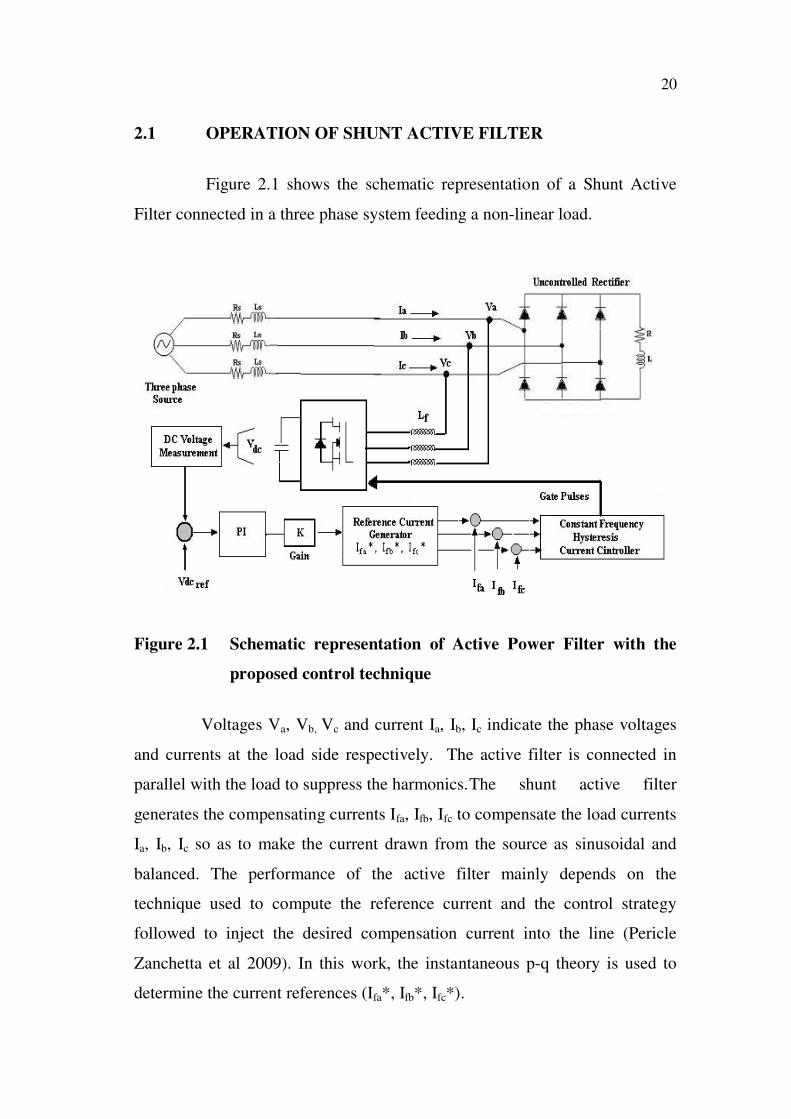
Figure 2.1 shows the schematic representation of a Shunt Active
Filter connected in a three phase system feeding a non-linear load.
Figure 2.1 Schematic representation of Active Power Filter with the
proposed control technique
Voltages Va, Vb, Vc and current Ia, Ib, Ic indicate the phase voltages
and currents at the load side respectively. The active filter is connected in
parallel with the load to suppress the harmonics. The shunt active filter
generates the compensating currents Ifa, Ifb, Ifc to compensate the load currents
Ia, Ib, Ic so as to make the current drawn from the source as sinusoidal and
balanced. The performance of the active filter mainly depends on the
technique used to compute the reference current and the control strategy
followed to inject the desired compensation current into the line (Pericle
Zanchetta et al 2009). In this work, the instantaneous p-q theory is used to
determine the current references (Ifa*, Ifb*, Ifc*).

21
Another important task in the development of active filter is the
maintenance of constant DC voltage across the capacitor connected to the
inverter. This is necessary because there is energy loss due to conduction and
switching power losses associated with the diodes and IGBTs of the inverter
in Active power filter, which tend to reduce the value of voltage across the
DC capacitor.
2.1.1 Reference Current Extraction
Derivation of compensation current is the important part of active
filter control. The time domain methods are mainly used due to its speed with
less calculation compared to the frequency domain methods. Instantaneous
p-d theory (Joao Afonso et al 2000), one of the time domain methods is
followed in this work. The details of instantaneous p-q theory are presented
here.
The p-q theory is based on the transformation, and is known as
the Clarke Transformation. It transforms the three phase voltage and current
into stationary reference frame using the following equations:
c
b
a
V
V
V
V
V
2
3
2
30
2
1
2
11
3
2 (2.1)
c
b
a
I
I
I
I
I
2
3
2
30
2
1
2
11
3
2 (2.2)
22
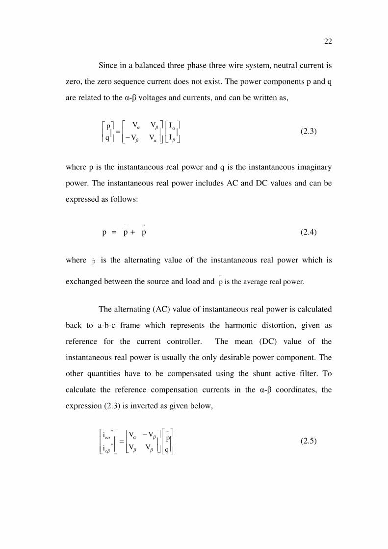
Since in a balanced three-phase three wire system, neutral current is
zero, the zero sequence current does not exist. The power components p and q
are related to the voltages and currents, and can be written as,
I
I
VV
VV
q
p(2.3)
where p is the instantaneous real power and q is the instantaneous imaginary
power. The instantaneous real power includes AC and DC values and can be
expressed as follows:
~
ppp (2.4)
where p~ is the alternating value of the instantaneous real power which is
exchanged between the source and load and p is the average real power.
The alternating (AC) value of instantaneous real power is calculated
back to a-b-c frame which represents the harmonic distortion, given as
reference for the current controller. The mean (DC) value of the
instantaneous real power is usually the only desirable power component. The
other quantities have to be compensated using the shunt active filter. To
calculate the reference compensation currents in the coordinates, the
expression (2.3) is inverted as given below,
q
p
VV
VV
i
i
c
c
~
*
*
(2.5)

23
where p~ is the alternating value of the instantaneous real power which is
exchanged between the source and load and q is the instantaneous imaginary
power corresponding to the power that is exchanged between the phases of
the load.
In order to obtain the reference compensation currents in the a-b-c
coordinates the inverse of the transformation is applied to eqn 2.2 and is given
as
*
*
*
*
*
2
3
2
1
2
3
2
1
01
c
c
cc
cb
ca
i
i
i
i
i
(2.6)
The eqn 2.6 gives the reference compensation current to be injected
to the system.
2.1.2 Hysteresis Current Control
The current control strategy plays an important role in the
development of shunt active filter. The hysteresis-band current control
method (Anshuman shukla et al 2007) is popularly used because of its
simplicity in implementation.
Hysteresis current controller derives the switching signals of the
inverter power switches in a manner that reduces the current error. The
switches are controlled asynchronously to ramp the current through the
inductor up and down so that it follows the reference. The current ramping up
and down between two limits is illustrated in Figure 2.2. When the current

24
through the inductor exceeds the upper hysteresis limit, a negative voltage is
applied by the inverter to the inductor. This causes the current through the
inductor to decrease. Once the current reaches the lower hysteresis limit, a
positive voltage is applied by the inverter through the inductor and this causes
the current to increase and the cycle repeats. The current controllers of the
three phases are designed to operate independently. They determine the
switching signals to the respective phase of the inverter.
Figure 2.2 Hysteresis Current Control Operation Waveform
This method has the drawbacks of variable switching frequency,
heavy interference between the phases in case of three phase active filter with
isolated neutral and irregularity of the modulation pulse position (Simone et al
2000). These drawbacks result in high current ripples, acoustic noise and
difficulty in designing input filter. In this chapter, a constant frequency
hysteresis current controller is proposed for shunt active filter applications.
The details of the proposed current control strategy are presented in the next
section.

25
2.1.3 DC Voltage Control
In shunt Active power filter, the output voltage of the inverter is
controlled by changing the switching pulses. This causes a flow of
instantaneous power into the inverter which charges/discharges the inverter
DC bus capacitor. Despite the resultant DC bus voltage fluctuations, its
average value remains constant in a lossless active filter. However, the
converter losses and active power filter exchange causes the capacitor voltage
to vary. Hence the DC bus capacitor must be designed to achieve two goals,
i.e., to comply with the minimum ripple requirement of the DC bus voltage
and to limit the DC bus voltage variation during load transients. In this work,
a PI controller is developed to control the DC bus voltage.
The input to the PI controller is DC voltage error e(t), which isgiven by
22)(ccref VVte (2.7)
Figure 2.3 shows the block diagram of the proposed PI Controller. In this
work, the value of pK and i
K are tuned by Zicholar Nihols method. The real
power requirement for voltage regulation is directly proportional to the square
of the dc voltage. Hence, square of the dc voltage is considered for calculating
the required real power to maintain constant voltage across the dc bus.
Figure 2.3 Block diagram of the DC voltage control using a PI controller
The controller adjusts the real power (Preg) requirement for voltage
regulation to keep the constant voltage across the capacitor.
26
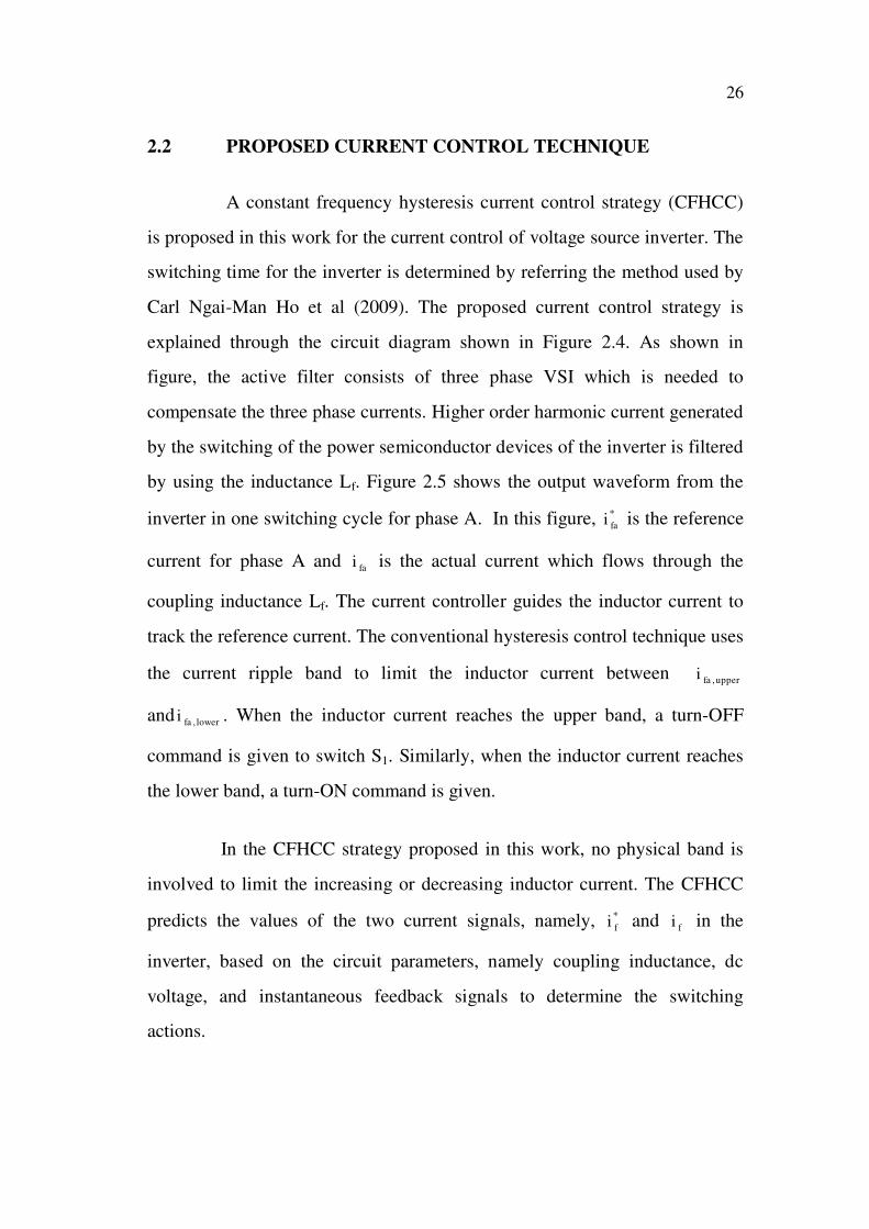
2.2 PROPOSED CURRENT CONTROL TECHNIQUE
A constant frequency hysteresis current control strategy (CFHCC)
is proposed in this work for the current control of voltage source inverter. The
switching time for the inverter is determined by referring the method used by
Carl Ngai-Man Ho et al (2009). The proposed current control strategy is
explained through the circuit diagram shown in Figure 2.4. As shown in
figure, the active filter consists of three phase VSI which is needed to
compensate the three phase currents. Higher order harmonic current generated
by the switching of the power semiconductor devices of the inverter is filtered
by using the inductance Lf. Figure 2.5 shows the output waveform from the
inverter in one switching cycle for phase A. In this figure, *
fai is the reference
current for phase A and fai is the actual current which flows through the
coupling inductance Lf. The current controller guides the inductor current to
track the reference current. The conventional hysteresis control technique uses
the current ripple band to limit the inductor current between upperfai ,
and lowerfai , . When the inductor current reaches the upper band, a turn-OFF
command is given to switch S1. Similarly, when the inductor current reaches
the lower band, a turn-ON command is given.
In the CFHCC strategy proposed in this work, no physical band is
involved to limit the increasing or decreasing inductor current. The CFHCC
predicts the values of the two current signals, namely, *
fi and fi in the
inverter, based on the circuit parameters, namely coupling inductance, dc
voltage, and instantaneous feedback signals to determine the switching
actions.

27
Figure 2.4 Circuit diagram of voltage source inverter based Shunt
Active Filter
Figure 2.5 Output Waveform of Inverter

28
As shown in Figure 2.5, the current waveform has been divided into
two sections namely, positive half cycle (t0–t2) and negative half cycle (t2–t4),
in one switching period. The controller determines the time for turn-ON and
turn-OFF actions to achieve the desired half switching period, T/2, in positive
and negative sections. At the same time, the controller predicts the value of
*
fi as well. The system is operated with bipolar pulse width modulation
switching. The development of control algorithm for CFHCC which drives
the inverter at a constant switching frequency is described below.
Figure 2.6 Equivalent Circuit (a) Turn ON b) Turn OFF
Figure 2.6 (a) shows the equivalent circuit of the inverter when the
switches S1 and S6 are in turn-ON condition. From the figure, the loop
equation can be written as,
0)( aON
fa
fdc Vdt
diLV (2.8)

29
From eqn (2.8),
f
adc
ON
fa
L
VV
dt
di)( (2.9)
Figure 2.6 (b) shows the equivalent circuit of the inverter when the switch S4
and S5 are in turn-ON condition. In this case the loop equation can be written
as,
0)(aOFF
fa
fdcV
dt
diLV (2.10)
From eqn (2.10)
f
adc
OFF
fa
L
VV
dt
di)( (2.11)
wheredc
V is the dc link voltage,a
V is the instantaneous grid voltage, and Lf is
the output inductance. The voltage drop across internal resistance of the
coupling inductor is neglected. To predict the value of *
fai an assumption has
to be made that is *
fai changes linearly over one switching cycle. Then, the
controller can predict the crossover point by considering the instantaneous
slope of *
fai .
2.2.1 Turn-OFF Criteria
At 1t , the inductor current and reference current can be expressed as
)()( ,1 ofaON
ON
fa
fa titdt
diti (2.12)

30
)()(*
,
*
1
*
ofaON
fa
fa titdt
diti (2.13)
From equations (2.12) and (2.13)
)()()()(*
*
,11
*
ofaofa
ON
fafa
ONfafa titidt
di
dt
dittiti (2.14)
In Figure 2.5, at t0,
)()(*
ofaofatiti (2.15)
Hence, in the positive section ( )20 tt , the instantaneous slope of
*
fai is given by
ON
fafa
ON
fafa
t
titi
dt
di
dt
di
,
11
*** )()(
(2.16)
Using the value of slope OFFt , is estimated as given below.
At 2t , the inductor current and reference current are expressed as
)()( 1,2 titdt
diti
faOFF
OFF
fa
fa (2.17)
)()( 1
*
,
*
2
*tit
dt
diti faOFF
fa
fa (2.18)
From equations (2.17) and (2.18)
)()()()( 22
**
,11
*titi
dt
di
dt
dittiti fafa
OFF
fafa
OFFfafa (2.19)

31
In Figure 2.5, at t0,
)()( 22
*titi fafa
)]/()/[(
)()(
*
11
*
,dtdidtdi
titit
faOFFfa
fafa
OFF (2.20)
By using eqns (2.8) to (2.11)
1
,1
*
1
,
1
)]()(([
2
ONfafaf
dcOFF
ttitiL
Vt (2.21)
The turn-OFF time is estimated using (2.21) with instantaneous
feedback signals. The turn-OFF criterion is the time of *
fafa ii in positive that
is equal to half switching cycle as shown in Figure 2.5. Thus
2,,
Ttt ONOFF and 0
*
fafa ii (2.22)
where T is the switching period. Based on eqns (2.20) and (2.21), the
controller can determine the turn-OFF action at the most suitable time.
2.2.2 Turn-ON Criteria
In the negative section )( 42 tt , the instantaneous slope of *
fai is
given by
OFF
fafa
OFF
fafa
t
titi
dt
di
dt
dif
,
33
**
)()((2.23)

32
Based on the slope, ONt , is predicted as
)]/()/[(
)()(*
33
*
,dtdidtdi
titit
faONfa
fafa
ON(2.24)
By using (2.8), (2.9), (2.23) and (2.24)
1
,33
*,
1
)]()(([
2
OFFfafaf
dc
ONttitiL
Vt (2.25)
From eqn 2.25 the turn-ON time is estimated with instantaneous
feedback signals. The turn-ON criterion is the time of *
fafa ii in negative that
is equal to half switching cycle as shown in Figure 2.5. Thus
2,,
Ttt
ONOFF and 0*
fafa ii (2.26)
It is the same as positive section. Based on eqns (2.22) and (2.26),
the controller can be designed. The gate pulses (g1 and g4) for the inverter
(Phase A) using the proposed control logic can be derived using the circuit
shown in Figure 2.7.

33
Figure 2.7 Implementation of proposed control strategy
[
The switching function (g3 g6 and g2 g5) for the other two legs of
the inverter is derived by calculating the ON/OFF time using the reference
currents *
fbi and *
fci respectively.
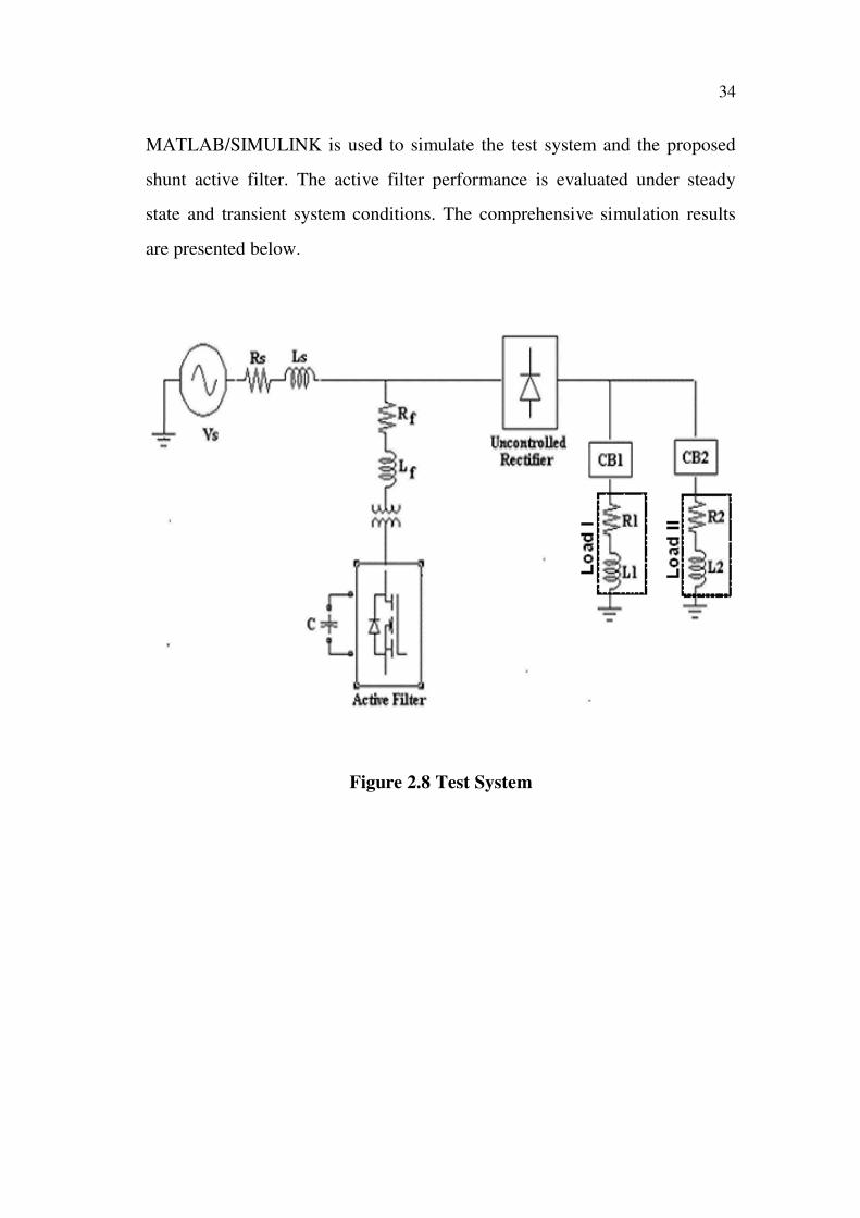
2.3 SIMULATION RESULTS
This section presents the details of the simulation carried out on a
test system. The test system consists of a three phase voltage source, and an
uncontrolled rectifier with RL loads connected through circuit breakers
(CB1 and CB2) as shown in Figure 2.8. The active filter with proposed
control strategy is connected to the test system through an inductor Lf. The
values of the circuit elements used in the simulation are given in Table 2.1.
The design steps to determine system parameters are given in Appendix 2.
34
MATLAB/SIMULINK is used to simulate the test system and the proposed
shunt active filter. The active filter performance is evaluated under steady
state and transient system conditions. The comprehensive simulation results
are presented below.
Figure 2.8 Test System

35
Table 2.1 System Parameters
Parameter Specification
Supply phase to phase voltage,
frequency415 V (rms), 50 Hz
Line Parameters (Rs, Ls) 1 , 1mH
Load Resistance (R1,R2) 70 , 50
Load Inductance (L1,L2) 37 mH, 3mH
Filter coupling Inductance (Lf) 3 mH, 0.5
Inverter DC bus capacitor 1mF
Vdc (reference) 700V
Sampling Time sec102 6
Switching Frequency 16 kHz
No of samples taken for FFT
calculation10000
A. Steady State Performance
First the system is simulated without the filter. In this case the
circuit breaker 1 is closed and circuit breaker 2 is opened. The three phase
source current waveform in this case is shown in Figure 2.9(a). Figure 2.9(b)
shows the harmonic spectrum of the distorted waveform. The total harmonic
distortion of the distorted line current is 26.34%. The methodology of
calculating THD is given in Appendix 1. From the harmonic spectrum, it is
evident that, the source current is distorted due to the dominancy of fifth and
seventh harmonic spectral components.

36
(a) Distorted three phase source current
(b) Harmonic Spectrum of the source current
Figure 2.9 Distorted line current and harmonic spectrum caused by
three phase uncontrolled rectifier
Next, an active filter with proposed control strategy is connected in
parallel with the load. A PI controller is used to maintain the constant voltage
across the DC side capacitor. Figure 2.10 shows the source current along with
the frequency spectrum in the presence of the active power filter with the
CFHCC scheme. The performance of the active filter with the proposed
control algorithm is found to be excellent, and the source current is practically
sinusoidal and it is in phase with the supply voltage as shown in Figure 2.11.
The THD of current in Phase A, B and C has reduced to 3.87%, 3.89% and
3.39%. It shows that the THD is very much reduced after connecting the
filter.
THD = 26.34%

37
During the filtering process, the inverter charges/discharges the
inverter DC bus capacitor. Despite the resultant DC bus voltage fluctuations,
its average value remains constant in a lossless active filter. However, the
converter losses and active power filter exchange cause the capacitor voltage
to vary. Hence, the DC bus capacitor must be designed to achieve two goals,
i.e., to comply with the minimum ripple requirement of the DC bus voltage
and to limit the DC bus voltage variation during load transients. A
proportional and integral controller is implemented to control the DC bus
voltage. By controlling the real power, the dc bus voltage can be varied.
Hence, the error between the actual voltage and the reference is given as input
to the PI controller. The controller generates an output value corresponding to
the error value. The output of the controller is the real power required to
maintain the reference dc voltage. The calculated Figure 2.12 shows the
constant voltage (700V) maintained by the PI controller across the capacitor.
Figure 2.10 Harmonic current filtering with proposed CFHCC
Technique

38
Figure 2.11 Waveform of Source voltage and Current in Phase A
Figure 2.12 DC Bus Voltage Maintenance using PI Control
For comparison, next the active filter is simulated with fixed
hysteresis band current control technique. The hysteresis current controller
with fixed band (HB=0.1A) has been used to generate the gate pulses for the
inverter. Figure 2.13 shows the performance of the shunt active filter with
fixed hysteresis current control technique. In this case, the THD has reduced
to 4.1% which is high compared to the THD obtained using the proposed
technique. Also, the distortion in the supply current is high due to high ripple.
Table 2.2 gives the comparison of the individual harmonic level of source
current and voltage between the proposed technique and the FHBCC
technique. From this comparison, it is clear that the source voltage and current

39
harmonics have greatly reduced in the proposed technique compared to the
FHBCC.
Table 2.2 Harmonic Contents of the supply current and voltage
Harmonic
Order
Individual Harmonic Content (% of fundamental)
Without
Filter
Filter with
FHBCC
Filter with
CFHCC
Current Voltage Current Voltage Current
3 0 0.01 0.5 0 0.03
5 23 0.12 1.5 0.11 1.27
7 12 0.12 1.52 0.13 1.03
9 0 0.01 0.12 0.01 0.07
11 9 0.3 1.61 0.28 1.34
13 7 0.23 1.45 0.23 1.1
15 0 0.02 0.26 0.01 0.15
17 5 0.39 1.33 0.39 1.0
19 4 0.25 0.9 0.25 0.2
THD(%) 26.34 3.3 4.1 2.91 3.89

40
Figure 2.13 Fixed HBCC Technique – Source Current with its
Harmonic Spectrum
Figure 2.14 Average Switching Frequency of the Inverter
41
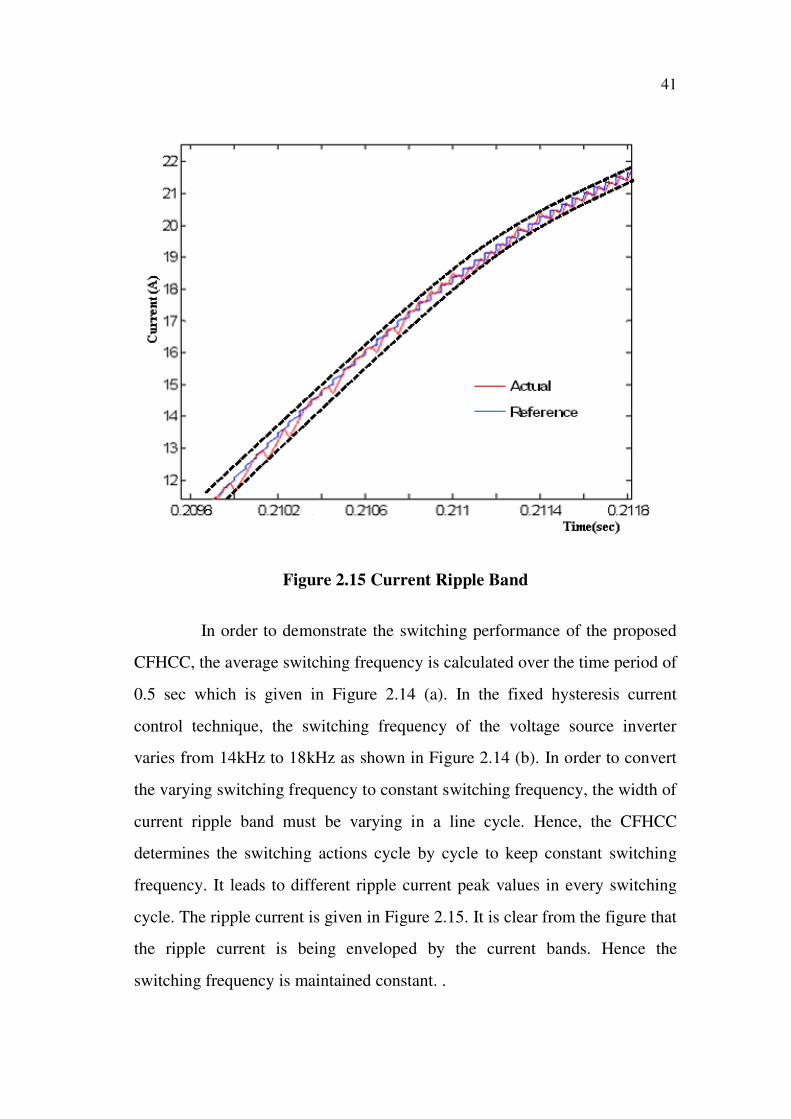
Figure 2.15 Current Ripple Band
In order to demonstrate the switching performance of the proposed
CFHCC, the average switching frequency is calculated over the time period of
0.5 sec which is given in Figure 2.14 (a). In the fixed hysteresis current
control technique, the switching frequency of the voltage source inverter
varies from 14kHz to 18kHz as shown in Figure 2.14 (b). In order to convert
the varying switching frequency to constant switching frequency, the width of
current ripple band must be varying in a line cycle. Hence, the CFHCC
determines the switching actions cycle by cycle to keep constant switching
frequency. It leads to different ripple current peak values in every switching
cycle. The ripple current is given in Figure 2.15. It is clear from the figure that
the ripple current is being enveloped by the current bands. Hence the
switching frequency is maintained constant. .

42
The proposed controller maintains the switching frequency at 16kHz
since it is designed for the switching period (ton+toff=T/2) of 1/16000/2 sec.
The periodogram of the inductor current is shown in Figure 2.16. From this
figure, it is evident that the switching frequency sharply concentrates at one
frequency, 16kHz.
Figure 2.16 Periodogram of Inductor Current
B. Transient Performance
To observe the transient characteristics of the proposed control
strategy, a step change in load current was applied. For this, the load I is
connected to the source upto 0.3 sec through circuit breaker I after that CB1
disconnect the load I from the source and CB2 connects the load II to the
source. Figure 2.17 (a) and (b) show the source current without shunt active
filter and with SAF respectively. The transient behavior of CFHCC is same as
that of the conventional fixed hysteresis control as shown in Figure 2.17(c).
But, unlike fixed hysteresis control, the proposed CFHCC is able to keep the

43
constant switching frequency after the transient period. But at transient time
(at 3 sec) there is a big current dip before the current returns to steady state as
shown in Figure 2.18. The reason for this is that the CFHCC predicts the
crossover point in each half switching period based on the instantaneous
current reference signal. When the current reference change occurs before the
command, the controller estimates incorrect turn-ON time since the initial
values of reference and actual current are same at the initial condition of the
timer.
Figure 2.17 Load and Source current waveform during step change in
load

44
cu
rren
t (A
)
Reference
Current
Actual Current
Time(sec)
Figure 2.18 Transient Response of the proposed Controller
2.4 CONCLUSION
This chapter has presented a Constant frequency hysteresis Current
Control Technique for developing the active filter. Instantaneous p-q theory
was employed for effectively computing the reference. The active filter was
simulated using MATLAB/ SIMULINK and the performance was analyzed in
a sample power system with a source and non-linear loads. The shunt active
filter is found to be effective to meet IEEE 519-1992 standard
recommendation on harmonic levels under ideal source voltage condition
with constant switching frequency. The proposed control technique has fast
dynamic response similar to conventional hysteresis control but it overcomes
the drawback of having variable switching frequency.