lm2696 3a, constant on time buck regulator (rev. b) · • constant frequency across input range...
TRANSCRIPT

RFB1
RFB2
SWL
COUT
VOUT
LM2696
DCATCHGNDFB
CBOOT
CBOOT
CEXT
EXTVCC
CSSCAVINCINSS
VIN
PVIN
AVIN
RONRON
SD
PGOODVPGOOD
VSDCSD
LM2696
www.ti.com SNVS375B –OCTOBER 2005–REVISED APRIL 2013
LM2696 3A, Constant On Time Buck RegulatorCheck for Samples: LM2696
1FEATURES DESCRIPTIONThe LM2696 is a pulse width modulation (PWM) buck
2• Input Voltage Range of 4.5V–24Vregulator capable of delivering up to 3A into a load.
• Constant On-Time The control loop utilizes a constant on-time control• No Compensation Needed scheme with input voltage feed forward. This provides
a topology that has excellent transient response• Maximum Load Current of 3Awithout the need for compensation. The input voltage• Switching Frequency of 100 kHz–500 kHz feed forward ensures that a constant switching
• Constant Frequency Across Input Range frequency is maintained across the entire VIN range.• TTL Compatible Shutdown Thresholds The LM2696 is capable of switching frequencies in• Low Standby Current of 12 µA the range of 100 kHz to 500 kHz. Combined with an
integrated 130 mΩ high side NMOS switch the• 130 mΩ Internal MOSFET SwitchLM2696 can utilize small sized external componentsand provide high efficiency. An internal soft-start andAPPLICATIONSpower-good flag are also provided to allow for simple
• High Efficiency Step-Down Switching sequencing between multiple regulators.Regulators
The LM2696 is available with an adjustable output in• LCD Monitors an exposed pad HTSSOP-16 package.• Set-Top Boxes
Typical Application Circuit
1
Please be aware that an important notice concerning availability, standard warranty, and use in critical applications ofTexas Instruments semiconductor products and disclaimers thereto appears at the end of this data sheet.
2All trademarks are the property of their respective owners.
PRODUCTION DATA information is current as of publication date. Copyright © 2005–2013, Texas Instruments IncorporatedProducts conform to specifications per the terms of the TexasInstruments standard warranty. Production processing does notnecessarily include testing of all parameters.

98 GNDN/C
107 SSFB
116 PGOODEXTVCC
125 RONAVIN
134 SDCBOOT
143 PVINSW
152SW
161SW
PVIN
PVIN
LM2696
SNVS375B –OCTOBER 2005–REVISED APRIL 2013 www.ti.com
Connection Diagram
Top View
Figure 1. HTSSOP-16 PackageSee Package Number PWP0016A
PIN DESCRIPTIONSPin # Name Function
1, 2, 3 SW Switching node
4 CBOOT Bootstrap capacitor input
5 AVIN Analog voltage input
6 EXTVCC Output of internal regulator for decoupling
7 FB Feedback signal from output
8 N/C No connect
9 GND Ground
10 SS Soft-start pin
11 PGOOD Power-good flag, open drain output
12 RON Sets the switch on-time dependent on current
13 SD Shutdown pin
14, 15, 16 PVIN Power voltage input
- Exposed Pad Must be connected to ground
These devices have limited built-in ESD protection. The leads should be shorted together or the device placed in conductive foamduring storage or handling to prevent electrostatic damage to the MOS gates.
2 Submit Documentation Feedback Copyright © 2005–2013, Texas Instruments Incorporated
Product Folder Links: LM2696

LM2696
www.ti.com SNVS375B –OCTOBER 2005–REVISED APRIL 2013
ABSOLUTE MAXIMUM RATINGS (1) (2) (3)
Voltages from the indicated pins to GND
AVIN −0.3V to +26V
PVIN −0.3V to (AVIN+0.3V)
CBOOT −0.3V to +33V
CBOOT to SW −0.3V to +7V
FB, SD, SS, PGOOD −0.3V to +7V
Storage Temperature Range −65°C to +150°C
Junction Temperature +150°C
Lead Temperature (Soldering, 10 sec.) 260°C
Minimum ESD Rating 1.5 kV
(1) Absolute Maximum Ratings indicate limits beyond which damage may occur to the device. Operating Ratings indicate conditions forwhich the device is intended to be functional, but do not ensure specific performance limits. For ensured specifications, see ElectricalCharacteristics.
(2) If Military/Aerospace specified devices are required, please contact the TI Sales Office/ Distributors for availability and specifications.(3) Without PCB copper enhancements. The maximum power dissipation must be derated at elevated temperatures and is limited by TJMAX
(maximum junction temperature), θJ-A (junction to ambient thermal resistance) and TA (ambient temperature). The maximum powerdissipation at any temperature is: PDissMAX = (TJMAX - TA) /θJ-A up to the value listed in the Absolute Maximum Ratings. θJ-A for HTSSOP-16 package is 38.1°C/W, TJMAX = 125°C.
OPERATING RANGEJunction Temperature −40°C to +125°C
AVIN to GND 4.5V to 24V
PVIN 4.5V to 24V
ELECTRICAL CHARACTERISTICSSpecifications with standard typeface are for TJ = 25°C, and those in boldface type apply over the full OperatingTemperature Range (TJ = −40°C to +125°C). Minimum and Maximum limits are specified through test, design or statisticalcorrelation. Typical values represent the most likely parametric norm at TJ = 25°C and are provided for reference purposesonly. Unless otherwise specified VIN = 12V.
Symbol Parameter Condition Min Typ Max Units
VFB Feedback Pin Voltage VIN = 4.5V to 24V 1.225 1.254 1.282 VISW = 0A to 3A
ICL Switch Current Limit VCBOOT = VSW + 5V 3.6 4.9 6.4 A
RDS_ON Switch On Resistance ISW = 3A 0.13 0.22 ΩIQ Operating Quiescent Current VFB = 1.5V 1.3 2 mA
VUVLO AVIN Under Voltage Lockout Rising VIN 3.9 4.125 4.3 V
VUVLO HYS AVIN Under Voltage Lockout Hysteresis 60 120 mV
ISD Shutdown Quiescent Current VSD = 0V 12 25 µA
kON Switch On-Time Constant ION = 50 µA to 100 µA 50 66 82 µA µs
VD ON RON Voltage 0.35 0.65 0.95 V
TOFF_MIN Minimum Off Time FB = 1.24V 165 250 nsFB = 0V 12 30 µs
TON MIN Minimum On-time 400 ns
VEXTV EXTVCC Voltage 3.30 3.65 4.00 V
ΔVEXTV EXTVCC Load Regulation IEXTV = 0 µA to 50 µA 0.03 0.5 %
VPWRGD PGOOD Threshold (PGOOD Transition With respect to VFB 91.5 93.5 95.5 %from Low to High)
VPG_HYS PGOOD Hysteresis 1 2.1 %
IOL PGOOD Low Sink Current VPGOOD = 0.4V 0.5 2 mA
IOH PGOOD High Leakage Current 50 nA
IFB Feedback Pin Bias Current VFB = 1.2V 0 nA
ISS_SOURCE Soft-Start Pin Source Current VSS = 0V 0.7 1 1.4 µA
Copyright © 2005–2013, Texas Instruments Incorporated Submit Documentation Feedback 3
Product Folder Links: LM2696

LM2696
SNVS375B –OCTOBER 2005–REVISED APRIL 2013 www.ti.com
ELECTRICAL CHARACTERISTICS (continued)Specifications with standard typeface are for TJ = 25°C, and those in boldface type apply over the full OperatingTemperature Range (TJ = −40°C to +125°C). Minimum and Maximum limits are specified through test, design or statisticalcorrelation. Typical values represent the most likely parametric norm at TJ = 25°C and are provided for reference purposesonly. Unless otherwise specified VIN = 12V.
Symbol Parameter Condition Min Typ Max Units
ISS SINK Soft-Start Pin Sink Current VSS = 1.2V 15 mAVSD = 0V
ISD Shutdown Pull-Up Current VSD = 0V 1 3 µA
VIH SD Pin Minimum High Input Level 1.8 V
VIL SD Pin Maximum Low Input Level 0.6 V
θJ-A Thermal Resistance 35.1 °C/W
4 Submit Documentation Feedback Copyright © 2005–2013, Texas Instruments Incorporated
Product Folder Links: LM2696

-40 -20 0 20 40 60 80 100 120
TEMPERATURE (oC)
EX
T V
CC
(V
)
3.635
3.64
3.645
3.65
3.655
3.66
3.665
3.67
-20 20 60 100 140
TEMPERATURE (oC)
0.6
0.7
0.8
0.9
1.0
1.1
1.2
1.3
1.4
1.5
VIL
AN
D V
IH (
V)
-60
VIH (V)
0 40 80 120-40
VIL (V)
0
2
4
6
8
10
12
14
16
18
20
4.5 7.5 10.5 13.5 16.5 24
VIN (V)
19.5 22.5
I Q (P
A)
-40 -20 0 20 40 60 80 100 120
TEMPERATURE (oC)
0
2
4
6
8
10
12
14
16
I Q (
SH
UT
DO
WN
) (P
A)
4.5 7.5 10.5 13.5 16.5 24
VIN (V)
19.5 22.5
1.05
1.1
1.15
1.2
1.25
1.3
1.35
1.4
1.45
1.5
1
I Q (P
A)
-40 -20 0 20 40 60 80 100 120
TEMPERATURE (oC)
I Q (
mA
)
1.12
1.14
1.16
1.18
1.2
1.22
1.24
1.26
1.28
1.30
1.32
LM2696
www.ti.com SNVS375B –OCTOBER 2005–REVISED APRIL 2013
TYPICAL PERFORMANCE CHARACTERISTICS
IQ vs Temp IQ vs VIN
Figure 2. Figure 3.
IQ in Shutdown vs Temp IQ vs VIN in Shutdown
Figure 4. Figure 5.
Shutdown Thresholds vs Temp EXTVCC vs Temp
Figure 6. Figure 7.
Copyright © 2005–2013, Texas Instruments Incorporated Submit Documentation Feedback 5
Product Folder Links: LM2696

0 50 100 150 200 250 300
ION (PA)
0
0.5
1
1.5
2
2.5
3
TO
N (P
s)
-40 -20 0 20 40 60 80 100 120
TEMPERATURE (oC)
168
170
172
174
176
178
180
TO
FF (
ns)
-40 -20 0 20 40 60 80 100 120
TEMPERATURE (°C)
TO
N .
I ON
(P
s . P
A)
64.7
64.9
65.1
65.3
65.5
65.7
65.9
66.1
66.3
66.5
-40 -20 0 20 40 60 80 100 120
TEMPERATURE (oC)
1.249
1.25
1.251
1.252
1.253
1.254
1.255
1.256
1.257
1.248
VF
B (
V)
4.5 7.5 10.5 13.5 16.5 24
VIN (V)
19.5 22.5
EX
TV
CC
(V
)
3.644
3.646
3.648
3.650
3.652
3.654
3.656
3.658
3.660
0 10 20 30 40 503.62
3.63
3.64
3.65
3.66
EX
T V
CC
(V
)
EXT VCC (PA)
LM2696
SNVS375B –OCTOBER 2005–REVISED APRIL 2013 www.ti.com
TYPICAL PERFORMANCE CHARACTERISTICS (continued)EXTVCC vs VIN EXTVCC vs Load Current
Figure 8. Figure 9.
Feedback Threshold Voltage vs Temp kON vs Temp
Figure 10. Figure 11.
Switch ON Time vs RON Pin Current Min Off-Time vs Temp
Figure 12. Figure 13.
6 Submit Documentation Feedback Copyright © 2005–2013, Texas Instruments Incorporated
Product Folder Links: LM2696

-40 -20 0 20 40 60 80 100 120
TEMPERATURE (oC)
VO
N (
V)
0
0.2
0.4
0.6
0.8
1
-40 -20 0 20 40 60 80 100 120
TEMPERATURE (oC)
CU
RR
EN
T L
IMIT
(A
)
4
4.2
4.4
4.6
4.8
5
5.2
5.4
100 200 300 400 5000.0
0.2
0.4
0.6
0.8
1.0D
UT
Y C
YC
LE
FREQUENCY (kHz)
Min Duty Cycle
Max Duty Cycle
-40 -20 0 20 40 60 80 100 120
TEMPERATURE (oC)
0
0.05
0.1
0.15
0.2
0.25
RD
S_O
N (:
)
LM2696
www.ti.com SNVS375B –OCTOBER 2005–REVISED APRIL 2013
TYPICAL PERFORMANCE CHARACTERISTICS (continued)Max and Min Duty-Cycle vs Freq
(Min TON = 400 ns, Min TOFF = 200 ns) FET Resistance vs Temp
Figure 14. Figure 15.
RON Pin Voltage vs Temp Current Limit vs Temp
Figure 16. Figure 17.
Copyright © 2005–2013, Texas Instruments Incorporated Submit Documentation Feedback 7
Product Folder Links: LM2696
1.25V
Q
QS
R
FB
AVIN
SW
GND
6V INTERNALSUB
REGULATOR
ON TIMER
DRIVER
CBOOT
LEVELSHIFT
RONTHERMAL
SHUTDOWN
4.8A
CURRENT LIMITOFF TIMER
Q
START
COMPLETE
Ron
LM2696
UVLO
FB
REGULATIONCOMPARATOR
SD
Q
OFF TIMER
EXTVCC
SD
PGOOD
94% x Vbg
UNDER-VOLTAGECOMPARATOR
Shutdown
PVIN
SS 1 PA
1.25V
3.65VINTERNAL LDO
SD
BUCKSWITCH
CURRENTSENSE
1 PA
LM2696
SNVS375B –OCTOBER 2005–REVISED APRIL 2013 www.ti.com
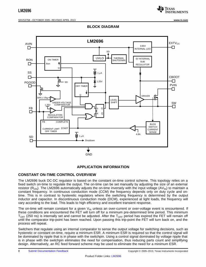
BLOCK DIAGRAM
APPLICATION INFORMATION
CONSTANT ON-TIME CONTROL OVERVIEW
The LM2696 buck DC-DC regulator is based on the constant on-time control scheme. This topology relies on afixed switch on-time to regulate the output. The on-time can be set manually by adjusting the size of an externalresistor (RON). The LM2696 automatically adjusts the on-time inversely with the input voltage (AVIN) to maintain aconstant frequency. In continuous conduction mode (CCM) the frequency depends only on duty cycle and on-time. This is in contrast to hysteretic regulators where the switching frequency is determined by the outputinductor and capacitor. In discontinuous conduction mode (DCM), experienced at light loads, the frequency willvary according to the load. This leads to high efficiency and excellent transient response.
The on-time will remain constant for a given VIN unless an over-current or over-voltage event is encountered. Ifthese conditions are encountered the FET will turn off for a minimum pre-determined time period. This minimumTOFF (250 ns) is internally set and cannot be adjusted. After the TOFF period has expired the FET will remain offuntil the comparator trip-point has been reached. Upon passing this trip-point the FET will turn back on, and theprocess will repeat.
Switchers that regulate using an internal comparator to sense the output voltage for switching decisions, such ashysteretic or constant on-time, require a minimum ESR. A minimum ESR is required so that the control signal willbe dominated by ripple that is in phase with the switchpin. Using a control signal dominated by voltage ripple thatis in phase with the switchpin eliminates the need for compensation, thus reducing parts count and simplifyingdesign. Alternatively, an RC feed forward scheme may be used to eliminate the need for a minimum ESR.
8 Submit Documentation Feedback Copyright © 2005–2013, Texas Instruments Incorporated
Product Folder Links: LM2696

D =VOUT + VD
VIN + VD - VSW
D =VOUT
VIN
LM2696
www.ti.com SNVS375B –OCTOBER 2005–REVISED APRIL 2013
INTERNAL OPERATION UNDER-VOLTAGE COMPARATOR
An internal comparator is used to monitor the feedback pin for sensing under-voltage output events. If the outputvoltage drops below the UVP threshold the power-good flag will fall.
ON-TIME GENERATOR SHUTDOWN
The on-time for the LM2696 is inversely proportional to the input voltage. This scheme of on-time controlmaintains a constant frequency over the input voltage range. The on-time can be adjusted by using an externalresistor connected between the PVIN and RON pins.
CURRENT LIMIT
The LM2696 contains an intelligent current limit off-timer. If the peak current in the internal FET exceeds 4.9A thepresent on-time is terminated; this is a cycle-by-cycle current limit. Following the termination of the on-time, anon-resetable extended off timer is initiated. The length of the off-time is proportional to the feedback voltage.When FB = 0V the off-time is preset to 20 µs. This condition is often a result of in short circuit operation when amaximum amount of off-time is required. This amount of time ensures safe short circuit operation up to themaximum input voltage of 24V.
In cases of overload (not complete short circuit, FB > 0V) the current limit off-time is reduced. Reduction of theoff-time during smaller overloads reduces the amount of fold back. This also reduces the initial startup time.
N-CHANNEL HIGH SIDE SWITCH AND DRIVER
The LM2696 utilizes an integrated N-Channel high side switch and associated floating high voltage gate driver.This gate driver circuit works in conjunction with an external bootstrap capacitor and an internal diode. Theminimum off-time (165 ns) is set to ensure that the bootstrap capacitor has sufficient time to charge.
THERMAL SHUTDOWN
An internal thermal sensor is incorporated to monitor the die temperature. If the die temp exceeds 165ºC then thesensor will trip causing the part to stop switching. Soft-start will restart after the temperature falls below 155ºC.
COMPONENT SELECTION
As with any DC-DC converter, numerous trade-offs are present that allow the designer to optimize a design forefficiency, size and performance. These trade-offs are taken into consideration throughout this section.
The first calculation for any buck converter is duty cycle. Ignoring voltage drops associated with parasiticresistances and non-ideal components, the duty cycle may be expressed as:
(1)
A duty cycle relationship that considers the voltage drop across the internal FET and voltage drop across theexternal catch diode may be expressed as:
Where• VD is the forward voltage of the external catch diode (DCATCH)• VSW is the voltage drop across the internal FET. (2)
FREQUENCY SELECTION
Switching frequency affects the selection of the output inductor, capacitor, and overall efficiency. The trade-offsin frequency selection may be summarized as; higher switching frequencies permit use of smaller inductorspossibly saving board space at the trade-off of lower efficiency. It is recommended that a nominal frequency of300 kHz should be used in the initial stages of design and iterated if necessary.
Copyright © 2005–2013, Texas Instruments Incorporated Submit Documentation Feedback 9
Product Folder Links: LM2696

L =(VIN - VOUT) D
0.3 fSW IOUT
'IL =(VIN - VOUT) D
L fSW
fSW =D
TON103 kHz
RON =(VIN - VD) '
106
kON ISW k
TON =kON RON
VIN - VD10-3 Ps
LM2696
SNVS375B –OCTOBER 2005–REVISED APRIL 2013 www.ti.com
The switching frequency of the LM2696 is set by the resistor connected to the RON pin. This resistor controls thecurrent flowing into the RON pin and is directly related to the on-time pulse. Connecting a resistor from this pin toPVIN allows the switching frequency to remain constant as the input voltage changes. In normal operation thispin is approximately 0.65V above GND. In shutdown, this pin becomes a high impedance node to prevent currentflow.
The ON time may be expressed as:
where• VIN is the voltage at the high side of the RON resistor (typically PVIN)• VD is the diode voltage present at the RON pin (0.65V typical)• RON is in kΩ• kON is a constant value set internally (66 µA•µs nominal). (3)
This equation can be re-arranged such that RON is a function of switching frequency:
where• fSW is in kHz. (4)
In CCM the frequency may be determined using the relationship:
(5)
(TON is in µs)
Which is typically used to set the switching frequency.
Under no condition should a bypass capacitor be connected to the RON pin. Doing so couples any ACperturbations into the pin and prevents proper operation.
INDUCTOR SELECTION
Selecting an inductor is a process that may require several iterations. The reason for this is that the size of theinductor influences the amount of ripple present at the output that is critical to the stability of an adaptive on-timecircuit. Typically, an inductor is selected such that the maximum peak-to-peak ripple current is equal to 30% ofthe maximum load current. The inductor current ripple (ΔIL) may be expressed as:
(6)
Therefore, L can be initially set to the following by applying the 30% guideline:
(7)
The other features of the inductor that should be taken into account are saturation current and core material. Ashielded inductor or low profile unshielded inductor is recommended to reduce EMI.
OUTPUT CAPACITOR
The output capacitor size and ESR have a direct affect on the stability of the loop. This is because the adaptiveon-time control scheme works by sensing the output voltage ripple and switching appropriately. The outputvoltage ripple on a buck converter can be approximated by assuming that the AC inductor ripple current flowsentirely into the output capacitor and the ESR of the capacitor creates the voltage ripple. This is expressed as:
ΔVOUT≈ ΔIL • RESR (8)
10 Submit Documentation Feedback Copyright © 2005–2013, Texas Instruments Incorporated
Product Folder Links: LM2696

Cff_MAX =(VIN_MIN - VFB) x TON_MIN
0.03V x RffpF
Rff RFB1
RFB2Cff
SW
FB
L
COUT
VOUT
H =VOUT
VFB=
VOUT
1.25V
LM2696
www.ti.com SNVS375B –OCTOBER 2005–REVISED APRIL 2013
To ensure stability, two constraints need to be met. These constraints are the voltage ripple at the feedback pinmust be greater than some minimum value and the voltage ripple must be in phase with the switch pin.
The ripple voltage necessary at the feedback pin may be estimated using the following relationship:ΔVFB > −0.057 • fSW + 35
where• fSW is in kHz• ΔVFB is in mV. (9)
This minimum ripple voltage is necessary in order for the comparator to initiate switching. The voltage ripple atthe feedback pin must be in-phase with the switch. Because the ripple due to the capacitor charging andcapacitor ESR are out of phase, the ripple due to capacitor ESR must dominate.
The ripple at the output may be calculated by multiplying the feedback ripple voltage by the gain seen throughthe feedback resistors. This gain H may be expressed as:
(10)
To simplify design and eliminate the need for high ESR output capacitors, an RC network may be used to feedforward a signal from the switchpin to the feedback (FB) pin. See the ‘RIPPLE FEED FORWARD’ section formore details.
Typically, the best performance is obtained using POSCAPs, SP CAPs, tantalum, Niobium Oxide, or similarchemistry type capacitors. Low ESR ceramic capacitors may be used in conjunction with the RC feed forwardscheme; however, the feed forward voltage at the feedback pin must be greater than 30 mV.
RIPPLE FEED FORWARD
An RC network may be used to eliminate the need for high ESR capacitors. Such a network is connected asshown in Figure 18.
Figure 18. RC Feed Forward Network
The value of Rff should be large in order to prevent any potential offset in VOUT. Typically the value of Rff is on theorder of 1 MΩ and the value of RFB1 should be less than 10 kΩ. The large difference in resistor values minimizesoutput voltage offset errors in DCM. The value of the capacitor may be selected using the following relationship:
where• on-time (TON_MIN) is in µs• resistance (Rff) is in MΩ. (11)
Copyright © 2005–2013, Texas Instruments Incorporated Submit Documentation Feedback 11
Product Folder Links: LM2696

ICIN_RMS = IOUT D(1 - D)
ICIN_RMS = IOUT
'IL2
12 IOUT21 - D + ¸¹
ᬩ
§D
12
'IL RESRVOUT = VOUT_AVG - 'VOUT = VOUT_AVG - 12
VOUT_AVG
Time
VREF
VOUT
'VOUT
RFB1 = RFB2
VOUT
VFB- 1¸¹
ᬩ
§
LM2696
SNVS375B –OCTOBER 2005–REVISED APRIL 2013 www.ti.com
FEEDBACK RESISTORS
The feedback resistors are used to scale the output voltage to the internal reference value such that the loop canbe regulated. The feedback resistors should not be made arbitrarily large as this creates a high impedance nodeat the feedback pin that is more susceptible to noise. Typically, RFB2 is on the order of 1 kΩ. To calculate thevalue of RFB1, one may use the relationship:
Where• VFB is the internal reference voltage that can be found in the ELECTRICAL CHARACTERISTICS table (1.254V
typical). (12)
The output voltage value can be set in a precise manner by taking into account the fact that the referencevoltage is regulating the bottom of the output ripple as opposed to the average value. This relationship is shownin Figure 19.
Figure 19. Average and Ripple Output Voltages
It can be seen that the average output voltage is higher than the gained up reference by exactly half the outputvoltage ripple. The output voltage may then be appended according to the voltage ripple. The appended VOUTterm may be expressed using the relationship:
(13)
One should note that for high output voltages (>5V), a load of approximately 15 mA may be required for theoutput voltage to reach the desired value.
INPUT CAPACITOR
Because PVIN is the power rail from which the output voltage is derived, the input capacitor is typically selectedaccording to the load current. In general, package size and ESR determine the current capacity of a capacitor. Ifthese criteria are met, there should be enough capacitance to prevent impedance interactions with the source. Ingeneral, it is recommended to use a low ESR, high capacitance electrolytic and ceramic capacitor in parallel.Using two capacitors in parallel ensures adequate capacitance and low ESR over the operating range. TheSanyo MV-WX series electrolytic capacitors and a ceramic capacitor with X5R or X7R dielectric are an excellentcombination. To calculate the input capacitor RMS, one may use the following relationship:
(14)
that can be approximated by,
(15)
Typical values are 470 µF for the electrolytic capacitor and 0.1 µF for the ceramic capacitor.
12 Submit Documentation Feedback Copyright © 2005–2013, Texas Instruments Incorporated
Product Folder Links: LM2696

tSS_MIN =COUTVOUT
3A
tSS =1.25V CSS
ISS
LM2696
www.ti.com SNVS375B –OCTOBER 2005–REVISED APRIL 2013
AVIN CAPACITOR
AVIN is the analog bias rail of the device. It should be bypassed externally with a small (1 µF) ceramic capacitorto prevent unwanted noise from entering the device. In a shutdown state the current needed by AVIN will drop toapproximately 12 µA, providing a low power sleep state.
In most cases of operation, AVIN is connected to PVIN; however, it is possible to have split rail operation whereAVIN is at a higher voltage than PVIN. AVIN should never be lower than PVIN. Splitting the rails allows the powerconversion to occur from a lower rail than the AVIN operating range.
SOFT-START CAPACITOR
The SS capacitor is used to slowly ramp the reference from 0V to its final value of 1.25V (during shutdown thispin will be discharged to 0V). This controlled startup ability eliminates large in-rush currents in an attempt tocharge up the output capacitor. By changing the value of this capacitor, the duration of the startup may bechanged accordingly. The startup time may be calculated using the following relationship:
Where• ISS is the soft-start pin source current (1 µA typical) that may be found in the ELECTRICAL
CHARACTERISTICS table. (16)
While the CSS capacitor can be sized to meet the startup requirements, there are limitations to its size. If thecapacitor is too small, the soft-start will have little effect as the reference voltage is rising faster than the outputcapacitor can be charged causing the part to go into current limit. Therefore a minimum soft-start time should betaken into account. This can be determined by:
(17)
While COUT and VOUT control the slew rate of the output voltage, the total amount of time the LM2696 takes tostartup is dependent on two other terms. See the “ Startup” section for more information.
EXTVCC CAPACITOR
External VCC is a 3.65V rail generated by an internal sub-regulator that powers the parts internal circuitry. Thisrail should be bypassed with a 1 µF ceramic capacitor (X5R or equivalent dielectric). Although EXTVCC is forinternal use, it can be used as an external rail for extremely light loads (<50 µA). If EXTVCC is accidentallyshorted to GND the part is protected by a 5 mA current limit. This rail also has an under-voltage lockout that willprevent the part from switching if the EXTVCC voltage drops.
SHUTDOWN
The state of the shutdown pin enables the device or places it in a sleep state. This pin has an internal pull-upand may be left floating or connected to a high logic level. Connecting this pin to GND will shutdown the part.Shutting down the part will prevent the part from switching and reduce the quiescent current drawn by the part.This pin must be bypassed with a 1 nF ceramic capacitor (X5R or Y5V) to ensure proper logic thresholds.
CBOOT CAPACITOR
The purpose of an external bootstrap capacitor is to turn the FET on by using the SW node as a pedestal. Thisallows the voltage on the CBOOT pin to be greater than VIN. Whenever the catch diode is conducting and theSW node is at GND, an internal diode will conduct that charges the CBOOT capacitor to approximately 4V.When the SW node rises, the CBOOT pin will rise to approximately 4V above the SW node. For optimalperformance, a 0.1 µF ceramic capacitor (X5R or equivalent dielectric) should be used.
Copyright © 2005–2013, Texas Instruments Incorporated Submit Documentation Feedback 13
Product Folder Links: LM2696

Total Startup Time
TSS200 Ps730 Ps
VOUT
ExtVCC
VIN
LM2696
SNVS375B –OCTOBER 2005–REVISED APRIL 2013 www.ti.com
PGOOD RESISTOR
The PGOOD resistor is used to pull the PGOOD pin high whenever a steady state operating range is achieved.This resistor needs to be sized to prevent excessive current from flowing into the PGOOD pin whenever the opendrain FET is turned on. The recommendation is to use a 10 kΩ–100 kΩ resistor. This range of values is acompromise between rise time and power dissipation.
CATCH DIODE
The catch or freewheeling diode acts as the bottom switch in a non-synchronous buck switcher. Because of this,the diode has to handle the full output current whenever the FET is not conducting. Therefore, it must be sizedappropriately to handle the current. The average current through the diode can be calculated by the equation:
ID_AVG = IOUT•(1–D) (18)
Care should also be taken to ensure that the reverse voltage rating of the diode is adequate. Whenever the FETis conducting the voltage across the diode will be approximately equal to VIN. It is recommended to have areverse rating that is equal to 120% of VIN to ensure adequate guard banding against any ringing that couldoccur on the switch node.
Selection of the catch diode is critical to overall switcher performance. To obtain the optimal performance, aSchottky diode should be used due to their low forward voltage drop and fast recovery.
BYPASS CAPACITOR
A bypass capacitor must be used on the AVIN line to help decouple any noise that could interfere with the analogcircuitry. Typically, a small (1 µF) ceramic capacitor is placed as close as possible to the AVIN pin.
EXTERNAL OPERATION STARTUP
The total startup time, from the initial VIN rise to the time VOUT reaches its nominal value is determined by threeseparate steps. Upon the rise of VIN, the first step to occur is that the EXTVCC voltage has to reach its nominaloutput voltage of 3.65V before the internal circuitry is active. This time is dictated by the output capacitance (1µF) and the current limit of the regulator (5 mA typical), which will always be on the order of 730 µs. Uponreaching its steady state value, an internal delay of 200 µs will occur to ensure stable operation. Uponcompletion the LM2696 will begin switching and the output will rise. The rise time of the output will be governedby the soft-start capacitor. To highlight these three steps a timing diagram please refer to Figure 20.
Figure 20. Startup Timing Diagram
14 Submit Documentation Feedback Copyright © 2005–2013, Texas Instruments Incorporated
Product Folder Links: LM2696

SW Pin
VOUT
VL
I2
I1
I0
t1 t2 t3 t4 t5
InductorCurrent
NominalOutput
Voltage
LM2696
www.ti.com SNVS375B –OCTOBER 2005–REVISED APRIL 2013
UNDER- & OVER-VOLTAGE CONDITIONS
The LM2696 has a built in under-voltage comparator that controls PGOOD. Whenever the output voltage dropsbelow the set threshold, the PGOOD open drain FET will turn on pulling the pin to ground. For an over-voltageevent, there is no separate comparator to control PGOOD. However, the loop responds to prevent this eventfrom occurring because the error comparator is essentially sensing an OVP event. If the output is above thefeedback threshold then the part will not switch back on; therefore, the worst-case condition is one on-time pulse.
CURRENT LIMIT
The LM2696 utilizes a peak-detect current limit that senses the current through the FET when conducting andwill immediately terminate the on-pulse whenever the peak current exceeds the threshold (4.9A typical). Inaddition to terminating the present on-pulse, it enforces a mandatory off-time that is related to the feedbackvoltage.
If current limit trips and the feedback voltage is close to its nominal value of 1.25V, the off-time imposed will berelatively short. This is to prevent the output from dropping or any fold back from occurring if a momentary shortoccurred because of a transient or load glitch. If a short circuit were present, the off-time would extend toapproximately 12 µs. This ensures that the inductor current will reach a low value (approximately 0A) before thenext switching cycle occurs. The extended off-time prevents runaway conditions caused by hard shorts and highside blanking times.
If the part is in an over current condition, the output voltage will begin to drop as shown in Figure 21. If the outputvoltage is dropping and the current is below the current limit threshold, (I1), the part will assert a pulse (t2) after aminimum off-time (t1). This is in an attempt to raise the output voltage.
If the part is in an over current condition and the output voltage is below the regulation value (VL) as shown inFigure 21, the part will assert a pulse of minimal width (t4) and extend the off-time (t5). In the event that thevoltage is below the regulation value (VL) and the current is below the current limit value, the part will assert two(or more) pulses separated by some minimal off-time (t1).
Figure 21. Fault Condition Timing
Legend:
t1: Min off-time (165 ns typical)
t2: On-time (set by the user)
t3: Min off-time (165 ns typical)
t4: Blanking time (165 ns typical)
t5: Extended off-time (12 µs typical)
VL: UVP threshold
Copyright © 2005–2013, Texas Instruments Incorporated Submit Documentation Feedback 15
Product Folder Links: LM2696

IAVERAGE
Time (s)Continuous Conduction Mode (CCM)
Inductor Current
fSW =2 L VOUT IOUT
TON2 VIN (VIN - VOUT)
IBOUNDARY =(VIN - VOUT) D
2 L fSW
2.5 3 3.5 4 4.5 5 5.5
LOAD CURRENT (A)
0.2
0.4
0.6
0.8
1.0
1.2
1.4
NO
RM
ALIZ
ED
OU
TP
UT
VO
LT
AG
E
LM2696
SNVS375B –OCTOBER 2005–REVISED APRIL 2013 www.ti.com
The last benefit of this scheme is when the short circuit is removed, and full load is re-applied, the part willautomatically recover into the load. The variation in the off-time removes the constraints of other frequency foldback systems where the load would typically have to be reduced.
Figure 22. Normalized Output VoltageVersus Load Current
MODES OF OPERATION
Since the LM2696 utilizes a catch diode, whenever the load current is reduced to a point where the inductorripple is greater than two times the load current, the part will enter discontinuous operation. This is because thediode does not permit the inductor current to reverse direction. The point at which this occurs is the criticalconduction boundary and can be calculated by the following equation:
(19)
One advantage of the adaptive on-time control scheme is that during discontinuous conduction mode thefrequency will gradually decrease as the load current decreases. In DCM the switching frequency may bedetermined using the relationship:
(20)
It can be seen that there will always be some minimum switching frequency. The minimum switching frequency isdetermined by the parameters above and the minimum load presented by the feedback resistors. If there is someminimum frequency of operation the feedback resistors may be sized accordingly.
The adaptive on-time control scheme is effectively a pulse-skipping mode, but since it is not tied directly to aninternal clock, its pulse will only occur when needed. This is in contrast to schemes that synchronize to areference clock frequency. The constant on-time pulse-skipping/DCM mode minimizes output voltage ripple andmaximizes efficiency.
Several diagrams are shown in Figure 23 illustrating continuous conduction mode (CCM), discontinuousconduction mode (DCM), and the boundary condition.
16 Submit Documentation Feedback Copyright © 2005–2013, Texas Instruments Incorporated
Product Folder Links: LM2696

VAVERAGE
Time (s)
VH - VL = VRIPPLE
Output Voltage (V)
VH
VL VREGULATION
tON
tP
RFB1
RFB2
CD
SW
FB
L
COUT
VOUT
D
Time (s)Discontinuous Conduction Mode (DCM)
Switchnode Voltage
VIN
VOUT
IPEAK
Time (s)Discontinuous Conduction Mode (DCM)
Inductor Current
IAVERAGE
Time (s)DCM-CCM Boundary
Inductor Current
LM2696
www.ti.com SNVS375B –OCTOBER 2005–REVISED APRIL 2013
Figure 23. Modes of Operation
It can be seen that in DCM, whenever the inductor runs dry the SW node will become high impedance. Ringingwill occur as a result of the LC tank circuit formed by the inductor and the parasitic capacitance at the SW node.
Figure 24. Parasitic Tank Circuit at the Switchpin
LINE REGULATION
The LM2696 regulates to the lowest point of the output voltage (VL in Figure 25 ). This is to say that the outputvoltage may be represented by a waveform that is some average voltage with ripple. The LM2696 will regulate tothe trough of the ripple.
Figure 25. Average Output Voltage and Regulation Point
Copyright © 2005–2013, Texas Instruments Incorporated Submit Documentation Feedback 17
Product Folder Links: LM2696
Efficiency =Power_Out
Power_Out + Total_Power_Loss
12
'IL RESRVOUT = VL = VAVERAGE - VRIPPLE = VAVERAGE - 12
LM2696
SNVS375B –OCTOBER 2005–REVISED APRIL 2013 www.ti.com
The output voltage is given by the following relationship:
(21)
as discussed in the FEEDBACK RESISTORS section of this document.
TRANSIENT RESPONSE
Constant on-time architectures have inherently excellent transient line and load response. This is because thecontrol loop is extremely fast. Any change in the line or load conditions will result in a nearly instantaneousresponse in the PWM off time.
If one considers the switcher response to be nearly cycle-by-cycle, and amount of energy contained in a singlePWM pulse, there will be very little change in the output for a given change in the line or load.
EFFICIENCY
The constant on-time architecture features high efficiency even at light loads. The ability to achieve highefficiency at light loads is due to the fact that the off-time will become necessarily long at light loads. Havingextended the off-time, there is little mechanism for loss during this interval.
The efficiency is easily estimated using the following relationships:
Power loss due to FET:PFET = PC + PGC + PSW
Where• PC = D • (IOUT
2 • RDS_ON)• PGC = AVIN + VGS • QGS • fSW
• PSW = 0.5 • VIN · IOUT • (tr + tf) • fSW (22)
Typical values are:
RDS_ON = 130 mΩ
VGS = 4VQGS = 13.3 nCtr= 3.8 nstf= 4.5 ns Power loss due to catch diode:PD = (1-D) • (IOUT • Vf) (23)
Power loss due to DCR and ESR:PDCR = IOUT
2 • RDCR (24)PESR_OUTPUT = IRIPPLE
2/√12 • RESR_OUTPUT (25)PESR_INPUT = IOUT
2(D(1-D)) • RESR_INPUT (26)
Power loss due to Controller:PCONT = VIN • IQ (27)IQ is typically 1.3 mA (28)
The efficiency may be calculated as shown below:Total power loss = PFET + PD + PDCR + PESR_OUTPUT + PESR_INPUT + PCONT (29)Power Out = IOUT • VOUT (30)
(31)
18 Submit Documentation Feedback Copyright © 2005–2013, Texas Instruments Incorporated
Product Folder Links: LM2696

RFB1
RFB2
SWL
COUT
VOUT
LM2696
DCATCHGND
FB
CBOOT
CBOOT
CEXT
ExtVCC
CSSCIN
SS
PVIN
AVIN
RON
RON
SD
PGOOD
VIN
LM2696
www.ti.com SNVS375B –OCTOBER 2005–REVISED APRIL 2013
PRE-BIAS LOAD STARTUP
Should the LM2696 start into a pre-biased load the output will not be pulled low. This is because the part isasynchronous and cannot sink current. The part will respond to a pre-biased load by simply enabling PWM highor extending the off-time until regulation is achieved. This is to say that if the output voltage is greater than theregulation voltage the off-time will extend until the voltage discharges through the feedback resistors. If the loadvoltage is greater than the regulation voltage, a series of pulses will charge the output capacitor to its regulationvoltage.
THERMAL CONSIDERATIONS
The thermal characteristics of the LM2696 are specified using the parameter θJA, which relates the junctiontemperature to the ambient temperature. While the value of θJA is specific to a given set of test parameters(including board thickness, number of layers, orientation, etc), it provides the user with a common point ofreference.
To obtain an estimate of a devices junction temperature, one may use the following relationship:TJ = PIN (1-Efficiency) x θJA + TA
Where• TJ is the junction temperature in ºC• PIN is the input power in Watts (PIN = VIN·IIN)• θJA is the thermal coefficient of the LM2696• TA is the ambient temperature in ºC (32)
LAYOUT CONSIDERATIONS
The LM2696 regulation and under-voltage comparators are very fast and will respond to short duration noisepulses. Layout considerations are therefore critical for optimum performance. The components at pins 5, 6, 7, 12and 13 should be as physically close as possible to the IC, thereby minimizing noise pickup in the PC traces. Ifthe internal dissipation of the LM2696 produces excessive junction temperatures during normal operation, gooduse of the PC board’s ground plane can help considerably to dissipate heat. The exposed pad on the bottom ofthe HTSSOP-16 package can be soldered to a ground plane on the PC board, and that plane should extend outfrom beneath the IC to help dissipate the heat. Use of several vias beneath the part is also an effective methodof conducting heat. Additionally, the use of wide PC board traces, where possible, can also help conduct heataway from the IC. Judicious positioning of the PC board within the end product, along with use of any availableair flow (forced or natural convection) can help reduce the junction temperatures. Traces in the power plane(Figure 26) should be short and wide to minimize the trace impedance; they should also occupy the smallestarea that is reasonable to minimize EMI. Sizing the power plane traces is a tradeoff between current capacity,inductance, and thermal dissipation. For more information on layout considerations, please refer to TI ApplicationNote AN-1229.
Figure 26. Bold Traces Are In The Power Plane
Copyright © 2005–2013, Texas Instruments Incorporated Submit Documentation Feedback 19
Product Folder Links: LM2696
CIN
AVIN
CBOOT
SW
FB
PGOOD
RON
LM2696
VIN VOUT
RFB1
RFB2
GND
COUT
RON
PVIN
SD
CSSSS
EXTVCCCEXT
CBOOT
DCATCH
L
CAVIN
CSD
CBY
VPGOOD
VSD
LM2696
SNVS375B –OCTOBER 2005–REVISED APRIL 2013 www.ti.com
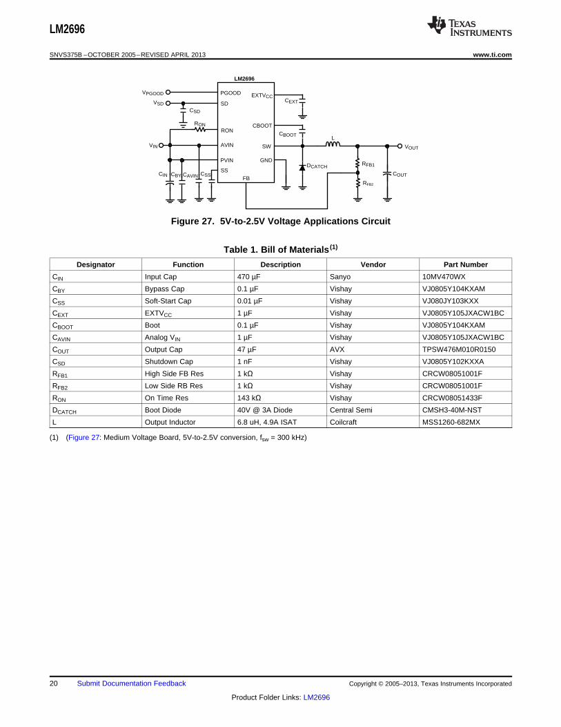
Figure 27. 5V-to-2.5V Voltage Applications Circuit
Table 1. Bill of Materials (1)
Designator Function Description Vendor Part Number
CIN Input Cap 470 µF Sanyo 10MV470WX
CBY Bypass Cap 0.1 µF Vishay VJ0805Y104KXAM
CSS Soft-Start Cap 0.01 µF Vishay VJ080JY103KXX
CEXT EXTVCC 1 µF Vishay VJ0805Y105JXACW1BC
CBOOT Boot 0.1 µF Vishay VJ0805Y104KXAM
CAVIN Analog VIN 1 µF Vishay VJ0805Y105JXACW1BC
COUT Output Cap 47 µF AVX TPSW476M010R0150
CSD Shutdown Cap 1 nF Vishay VJ0805Y102KXXA
RFB1 High Side FB Res 1 kΩ Vishay CRCW08051001F
RFB2 Low Side RB Res 1 kΩ Vishay CRCW08051001F
RON On Time Res 143 kΩ Vishay CRCW08051433F
DCATCH Boot Diode 40V @ 3A Diode Central Semi CMSH3-40M-NST
L Output Inductor 6.8 uH, 4.9A ISAT Coilcraft MSS1260-682MX
(1) (Figure 27: Medium Voltage Board, 5V-to-2.5V conversion, fsw = 300 kHz)
20 Submit Documentation Feedback Copyright © 2005–2013, Texas Instruments Incorporated
Product Folder Links: LM2696

CIN
AVIN
CBOOT
SW
FB
PGOOD
RON
LM2696
VIN VOUT
RFB1
RFB2
GND
COUT
RON
PVIN
SD
SS
EXTVCCCEXT
CBOOT
DCATCH
L
CSD
CBY
VPGOOD
VSD
Rff
Cff
CSSCAVIN
LM2696
www.ti.com SNVS375B –OCTOBER 2005–REVISED APRIL 2013
Figure 28. 12V-to 3.3V Voltage Applications Circuit
Table 2. Bill of Materials (1)
Designator Function Description Vendor Part Number
CIN Input Cap 560 µF Sanyo 35MV560WX
CBY Bypass Cap 0.1 µF Vishay VJ0805Y104KXAM
CSS Soft-Start Cap 0.01 µF Vishay VJ080JY103KXX
CEXT EXTVCC 1 µF Vishay VJ0805Y105JXACW1BC
CBOOT Boot 0.1 µF Vishay VJ0805Y104KXAM
CAVIN Analog VIN 1 µF Vishay VJ0805Y105JXACW1BC
COUT Output Cap 100 µF Sanyo 6SVPC100M
CSD Shutdown Cap 1 nF Vishay VJ0805Y102KXXA
Cff Feedforward Cap 560 pF Vishay VJ0805A561KXXA
Rff Feedforward Res 1 MΩ Vishay CRCW08051004F
RFB1 High Side FB Res 1.62 kΩ Vishay CRCW08051621F
RFB2 Low Side RB Res 1 kΩ Vishay CRCW08051001F
RON On Time Res 143 kΩ Vishay CRCW08051433F
DCATCH Boot Diode 40V @ 3A Diode Central Semi CMSH3-40M-NST
L Output Inductor 10 uH, 5.4A ISAT Coilcraft MSS1278-103MX
(1) (Figure 28: Medium Voltage Board, 12V-to-3.3V conversion, fsw = 300 kHz)
Copyright © 2005–2013, Texas Instruments Incorporated Submit Documentation Feedback 21
Product Folder Links: LM2696

LM2696
SNVS375B –OCTOBER 2005–REVISED APRIL 2013 www.ti.com
REVISION HISTORY
Changes from Revision A (April 2013) to Revision B Page
• Changed layout of National Data Sheet to TI format .......................................................................................................... 21
22 Submit Documentation Feedback Copyright © 2005–2013, Texas Instruments Incorporated
Product Folder Links: LM2696

PACKAGE OPTION ADDENDUM
www.ti.com 17-Mar-2017
Addendum-Page 1
PACKAGING INFORMATION
Orderable Device Status(1)
Package Type PackageDrawing
Pins PackageQty
Eco Plan(2)
Lead/Ball Finish(6)
MSL Peak Temp(3)
Op Temp (°C) Device Marking(4/5)
Samples
LM2696MXA/NOPB ACTIVE HTSSOP PWP 16 92 Green (RoHS& no Sb/Br)
CU SN Level-1-260C-UNLIM -40 to 125 2696MXA
LM2696MXAX/NOPB ACTIVE HTSSOP PWP 16 2500 Green (RoHS& no Sb/Br)
CU SN Level-1-260C-UNLIM -40 to 125 2696MXA
(1) The marketing status values are defined as follows:ACTIVE: Product device recommended for new designs.LIFEBUY: TI has announced that the device will be discontinued, and a lifetime-buy period is in effect.NRND: Not recommended for new designs. Device is in production to support existing customers, but TI does not recommend using this part in a new design.PREVIEW: Device has been announced but is not in production. Samples may or may not be available.OBSOLETE: TI has discontinued the production of the device.
(2) Eco Plan - The planned eco-friendly classification: Pb-Free (RoHS), Pb-Free (RoHS Exempt), or Green (RoHS & no Sb/Br) - please check http://www.ti.com/productcontent for the latest availabilityinformation and additional product content details.TBD: The Pb-Free/Green conversion plan has not been defined.Pb-Free (RoHS): TI's terms "Lead-Free" or "Pb-Free" mean semiconductor products that are compatible with the current RoHS requirements for all 6 substances, including the requirement thatlead not exceed 0.1% by weight in homogeneous materials. Where designed to be soldered at high temperatures, TI Pb-Free products are suitable for use in specified lead-free processes.Pb-Free (RoHS Exempt): This component has a RoHS exemption for either 1) lead-based flip-chip solder bumps used between the die and package, or 2) lead-based die adhesive used betweenthe die and leadframe. The component is otherwise considered Pb-Free (RoHS compatible) as defined above.Green (RoHS & no Sb/Br): TI defines "Green" to mean Pb-Free (RoHS compatible), and free of Bromine (Br) and Antimony (Sb) based flame retardants (Br or Sb do not exceed 0.1% by weightin homogeneous material)
(3) MSL, Peak Temp. - The Moisture Sensitivity Level rating according to the JEDEC industry standard classifications, and peak solder temperature.
(4) There may be additional marking, which relates to the logo, the lot trace code information, or the environmental category on the device.
(5) Multiple Device Markings will be inside parentheses. Only one Device Marking contained in parentheses and separated by a "~" will appear on a device. If a line is indented then it is a continuationof the previous line and the two combined represent the entire Device Marking for that device.
(6) Lead/Ball Finish - Orderable Devices may have multiple material finish options. Finish options are separated by a vertical ruled line. Lead/Ball Finish values may wrap to two lines if the finishvalue exceeds the maximum column width.
Important Information and Disclaimer:The information provided on this page represents TI's knowledge and belief as of the date that it is provided. TI bases its knowledge and belief on informationprovided by third parties, and makes no representation or warranty as to the accuracy of such information. Efforts are underway to better integrate information from third parties. TI has taken andcontinues to take reasonable steps to provide representative and accurate information but may not have conducted destructive testing or chemical analysis on incoming materials and chemicals.TI and TI suppliers consider certain information to be proprietary, and thus CAS numbers and other limited information may not be available for release.

PACKAGE OPTION ADDENDUM
www.ti.com 17-Mar-2017
Addendum-Page 2
In no event shall TI's liability arising out of such information exceed the total purchase price of the TI part(s) at issue in this document sold by TI to Customer on an annual basis.

TAPE AND REEL INFORMATION
*All dimensions are nominal
Device PackageType
PackageDrawing
Pins SPQ ReelDiameter
(mm)
ReelWidth
W1 (mm)
A0(mm)
B0(mm)
K0(mm)
P1(mm)
W(mm)
Pin1Quadrant
LM2696MXAX/NOPB HTSSOP PWP 16 2500 330.0 12.4 6.95 5.6 1.6 8.0 12.0 Q1
PACKAGE MATERIALS INFORMATION
www.ti.com 6-Nov-2015
Pack Materials-Page 1

*All dimensions are nominal
Device Package Type Package Drawing Pins SPQ Length (mm) Width (mm) Height (mm)
LM2696MXAX/NOPB HTSSOP PWP 16 2500 367.0 367.0 35.0
PACKAGE MATERIALS INFORMATION
www.ti.com 6-Nov-2015
Pack Materials-Page 2

www.ti.com
PACKAGE OUTLINE
C
TYP6.66.2
14X 0.65
16X 0.300.19
2X4.55
(0.15) TYP
0 - 80.150.05
3.32.7
3.32.7
2X 1.34 MAXNOTE 5
1.2 MAX
(1)
0.25GAGE PLANE
0.750.50
A
NOTE 3
5.14.9
B 4.54.3
4X 0.166 MAXNOTE 5
4214868/A 02/2017
PowerPAD HTSSOP - 1.2 mm max heightPWP0016APLASTIC SMALL OUTLINE
NOTES: 1. All linear dimensions are in millimeters. Any dimensions in parenthesis are for reference only. Dimensioning and tolerancing per ASME Y14.5M. 2. This drawing is subject to change without notice. 3. This dimension does not include mold flash, protrusions, or gate burrs. Mold flash, protrusions, or gate burrs shall not exceed 0.15 mm per side.4. Reference JEDEC registration MO-153.5. Features may not be present.
PowerPAD is a trademark of Texas Instruments.
TM
116
0.1 C A B
98
PIN 1 IDAREA
SEATING PLANE
0.1 C
SEE DETAIL A
DETAIL ATYPICAL
SCALE 2.400
THERMALPAD
17

www.ti.com
EXAMPLE BOARD LAYOUT
(5.8)
0.05 MAXALL AROUND
0.05 MINALL AROUND
16X (1.5)
16X (0.45)
14X (0.65)
(3.4)NOTE 9
(5)NOTE 9
(3.3)
(3.3)
( 0.2) TYPVIA (1.1) TYP
(1.1)TYP
4214868/A 02/2017
PowerPAD HTSSOP - 1.2 mm max heightPWP0016APLASTIC SMALL OUTLINE
SYMM
SYMM
SEE DETAILS
LAND PATTERN EXAMPLEEXPOSED METAL SHOWN
SCALE:10X
1
8 9
16
METAL COVEREDBY SOLDER MASK
SOLDER MASKDEFINED PAD
17
NOTES: (continued) 6. Publication IPC-7351 may have alternate designs. 7. Solder mask tolerances between and around signal pads can vary based on board fabrication site. 8. This package is designed to be soldered to a thermal pad on the board. For more information, see Texas Instruments literature numbers SLMA002 (www.ti.com/lit/slma002) and SLMA004 (www.ti.com/lit/slma004).9. Size of metal pad may vary due to creepage requirement.
TM
METALSOLDER MASKOPENING
NON SOLDER MASKDEFINED
SOLDER MASK DETAILSPADS 1-16
EXPOSEDMETAL
SOLDER MASKDEFINED
SOLDER MASKMETAL UNDER SOLDER MASK
OPENING
EXPOSEDMETAL

www.ti.com
EXAMPLE STENCIL DESIGN
16X (1.5)
16X (0.45)
(3.3)
(3.3)BASED ON
0.125 THICKSTENCIL
14X (0.65)
(R0.05) TYP
(5.8)
4214868/A 02/2017
PowerPAD HTSSOP - 1.2 mm max heightPWP0016APLASTIC SMALL OUTLINE
2.79 X 2.790.1753.01 X 3.010.15
3.3 X 3.3 (SHOWN)0.1253.69 X 3.690.1
SOLDER STENCILOPENING
STENCILTHICKNESS
NOTES: (continued) 10. Laser cutting apertures with trapezoidal walls and rounded corners may offer better paste release. IPC-7525 may have alternate design recommendations. 11. Board assembly site may have different recommendations for stencil design.
TM
SYMM
SYMM
1
89
16
BASED ON0.125 THICK
STENCIL
BY SOLDER MASKMETAL COVERED
SEE TABLE FORDIFFERENT OPENINGSFOR OTHER STENCILTHICKNESSES
SOLDER PASTE EXAMPLEEXPOSED PAD
100% PRINTED SOLDER COVERAGE BY AREASCALE:10X
17

IMPORTANT NOTICE
Texas Instruments Incorporated (TI) reserves the right to make corrections, enhancements, improvements and other changes to itssemiconductor products and services per JESD46, latest issue, and to discontinue any product or service per JESD48, latest issue. Buyersshould obtain the latest relevant information before placing orders and should verify that such information is current and complete.TI’s published terms of sale for semiconductor products (http://www.ti.com/sc/docs/stdterms.htm) apply to the sale of packaged integratedcircuit products that TI has qualified and released to market. Additional terms may apply to the use or sale of other types of TI products andservices.Reproduction of significant portions of TI information in TI data sheets is permissible only if reproduction is without alteration and isaccompanied by all associated warranties, conditions, limitations, and notices. TI is not responsible or liable for such reproduceddocumentation. Information of third parties may be subject to additional restrictions. Resale of TI products or services with statementsdifferent from or beyond the parameters stated by TI for that product or service voids all express and any implied warranties for theassociated TI product or service and is an unfair and deceptive business practice. TI is not responsible or liable for any such statements.Buyers and others who are developing systems that incorporate TI products (collectively, “Designers”) understand and agree that Designersremain responsible for using their independent analysis, evaluation and judgment in designing their applications and that Designers havefull and exclusive responsibility to assure the safety of Designers' applications and compliance of their applications (and of all TI productsused in or for Designers’ applications) with all applicable regulations, laws and other applicable requirements. Designer represents that, withrespect to their applications, Designer has all the necessary expertise to create and implement safeguards that (1) anticipate dangerousconsequences of failures, (2) monitor failures and their consequences, and (3) lessen the likelihood of failures that might cause harm andtake appropriate actions. Designer agrees that prior to using or distributing any applications that include TI products, Designer willthoroughly test such applications and the functionality of such TI products as used in such applications.TI’s provision of technical, application or other design advice, quality characterization, reliability data or other services or information,including, but not limited to, reference designs and materials relating to evaluation modules, (collectively, “TI Resources”) are intended toassist designers who are developing applications that incorporate TI products; by downloading, accessing or using TI Resources in anyway, Designer (individually or, if Designer is acting on behalf of a company, Designer’s company) agrees to use any particular TI Resourcesolely for this purpose and subject to the terms of this Notice.TI’s provision of TI Resources does not expand or otherwise alter TI’s applicable published warranties or warranty disclaimers for TIproducts, and no additional obligations or liabilities arise from TI providing such TI Resources. TI reserves the right to make corrections,enhancements, improvements and other changes to its TI Resources. TI has not conducted any testing other than that specificallydescribed in the published documentation for a particular TI Resource.Designer is authorized to use, copy and modify any individual TI Resource only in connection with the development of applications thatinclude the TI product(s) identified in such TI Resource. NO OTHER LICENSE, EXPRESS OR IMPLIED, BY ESTOPPEL OR OTHERWISETO ANY OTHER TI INTELLECTUAL PROPERTY RIGHT, AND NO LICENSE TO ANY TECHNOLOGY OR INTELLECTUAL PROPERTYRIGHT OF TI OR ANY THIRD PARTY IS GRANTED HEREIN, including but not limited to any patent right, copyright, mask work right, orother intellectual property right relating to any combination, machine, or process in which TI products or services are used. Informationregarding or referencing third-party products or services does not constitute a license to use such products or services, or a warranty orendorsement thereof. Use of TI Resources may require a license from a third party under the patents or other intellectual property of thethird party, or a license from TI under the patents or other intellectual property of TI.TI RESOURCES ARE PROVIDED “AS IS” AND WITH ALL FAULTS. TI DISCLAIMS ALL OTHER WARRANTIES ORREPRESENTATIONS, EXPRESS OR IMPLIED, REGARDING RESOURCES OR USE THEREOF, INCLUDING BUT NOT LIMITED TOACCURACY OR COMPLETENESS, TITLE, ANY EPIDEMIC FAILURE WARRANTY AND ANY IMPLIED WARRANTIES OFMERCHANTABILITY, FITNESS FOR A PARTICULAR PURPOSE, AND NON-INFRINGEMENT OF ANY THIRD PARTY INTELLECTUALPROPERTY RIGHTS. TI SHALL NOT BE LIABLE FOR AND SHALL NOT DEFEND OR INDEMNIFY DESIGNER AGAINST ANY CLAIM,INCLUDING BUT NOT LIMITED TO ANY INFRINGEMENT CLAIM THAT RELATES TO OR IS BASED ON ANY COMBINATION OFPRODUCTS EVEN IF DESCRIBED IN TI RESOURCES OR OTHERWISE. IN NO EVENT SHALL TI BE LIABLE FOR ANY ACTUAL,DIRECT, SPECIAL, COLLATERAL, INDIRECT, PUNITIVE, INCIDENTAL, CONSEQUENTIAL OR EXEMPLARY DAMAGES INCONNECTION WITH OR ARISING OUT OF TI RESOURCES OR USE THEREOF, AND REGARDLESS OF WHETHER TI HAS BEENADVISED OF THE POSSIBILITY OF SUCH DAMAGES.Unless TI has explicitly designated an individual product as meeting the requirements of a particular industry standard (e.g., ISO/TS 16949and ISO 26262), TI is not responsible for any failure to meet such industry standard requirements.Where TI specifically promotes products as facilitating functional safety or as compliant with industry functional safety standards, suchproducts are intended to help enable customers to design and create their own applications that meet applicable functional safety standardsand requirements. Using products in an application does not by itself establish any safety features in the application. Designers mustensure compliance with safety-related requirements and standards applicable to their applications. Designer may not use any TI products inlife-critical medical equipment unless authorized officers of the parties have executed a special contract specifically governing such use.Life-critical medical equipment is medical equipment where failure of such equipment would cause serious bodily injury or death (e.g., lifesupport, pacemakers, defibrillators, heart pumps, neurostimulators, and implantables). Such equipment includes, without limitation, allmedical devices identified by the U.S. Food and Drug Administration as Class III devices and equivalent classifications outside the U.S.TI may expressly designate certain products as completing a particular qualification (e.g., Q100, Military Grade, or Enhanced Product).Designers agree that it has the necessary expertise to select the product with the appropriate qualification designation for their applicationsand that proper product selection is at Designers’ own risk. Designers are solely responsible for compliance with all legal and regulatoryrequirements in connection with such selection.Designer will fully indemnify TI and its representatives against any damages, costs, losses, and/or liabilities arising out of Designer’s non-compliance with the terms and provisions of this Notice.
Mailing Address: Texas Instruments, Post Office Box 655303, Dallas, Texas 75265Copyright © 2017, Texas Instruments Incorporated