chapter 3 cathodic electrochemical deposition of undoped...
TRANSCRIPT
38
Chapter 3 Cathodic Electrochemical Deposition of Undoped and Doped Ceria
3.1 Introduction
There are numerous reports in the literature regarding the CELD of ceria [45-46, 53, 55,
57, 77-83], including a handful that generally list SOFCs as potential applications, but
with limited demonstration [48-52]. In addition, the contribution of electrogeneration of
base to CELD is well-documented [42-43]. However, insight related to the crucial SOFC
design criteria outlined in Section 1.4.1 is incomplete as most reports focus on as-
deposited composition and characterization, which is a broad area of study by itself due
to the large parameter space. Aside from grain growth evolution and brief mention in a
few studies, high temperature data are largely missing [49-51, 78, 80, 83]. Perhaps most
importantly, the vast majority of reports utilize non-porous, purely metallic substrates,
which violate the continuous pathway for ionic species requirement. To the best of the
author’s knowledge, a composite conducting/non-conducting substrate is mentioned only
once as a part of a larger study, in which the CELD of ceria was performed on a
nickel/yttria-stabilized zirconia cermet, but was not explored in detail [45]. Therefore,
this study assesses CELD according to (1) its compositional control, (2) the high
temperature behavior of its coatings, (3) its ability to meet minimum SOFC
configurational requirements, and (4) its potential for wide-ranging microstructural
optimization. In so doing, the electrogeneration of base/chemical precipitation
mechanism is validated with the assistance of others’ previous works [55, 82, 84-86], and
39
new insights are gained regarding the roles of the working potential and the depositing
species to the resulting microstructure, allowing a predictive, instead of haphazard,
approach to future CELD work.
In order to explore the flexibility of CELD as a fabrication tool, a range of
deposition conditions were examined, and a correspondingly wide range of reproducible
morphologies were obtained. Rather than describe the entirety of those results, two
primary types of morphologies are reported here—high surface area (HSA) coatings and
thin, planar films. These two microstructures are evaluated in the context of the HSA
coatings’ ability to be used as electrode components and the thin, planar films’ ability to
be used as electrolyte components.
As a visual aid to understand the general deposition mechanism and to distinguish
between the two experimental conditions probed in this chapter, a Ce-H2O-H2O2
Pourbaix diagram is shown in Fig. 3.1, adopted from reference [85]. Pourbaix diagrams
are pictorial representations of thermodynamic stabilities in the potential-pH parameter
space, although they do not contain any kinetics information. Initially, with no applied
potential, the pH sits in the range 2.5 – 4 (note that this diagram was constructed versus
the natural hydrogen electrode (NHE), whereas the working potentials in this manuscript
are referenced versus the standard calomel electrode (SCE), or +0.25 V vs. NHE). Once a
working potential is applied, the state of the system moves along a straight horizontal line
to the right, indicating that the electrolyte is becoming more basic. The black arrow on
the right-hand side vertical axis of Fig. 3.1 shows the working cathodic potential for the
HSA coating and the gray arrow indicates the working potential for thin films. The

40
applied potentials are used for the two morphologies, regardless of the composition of the electrolyte solution.
3.2 Experimental Details
3.2.1 Substrate Definition
The primary type of substrates used was a composite substrate, comprised of a supporting
YSZ base, on top of which various kinds of porous metal networks are overlaid. The
Fig. 3.1. Pourbaix diagram for the Ce-H2O-H2O2 system, reprinted with permission from [86]. The black arrow on the right-hand side, vertical axis represents a typical HSA depositing potential (-0.8 V
vs. SCE); the gray arrow represents the thin films’ depositing potential (-0.55 V vs. SCE). Final interfacial pH values are ~10.5.
41
pores in the metal films are necessary to allow for oxygen ion flux, and connectedness in
the metal networks is necessary to provide electronic conduction.
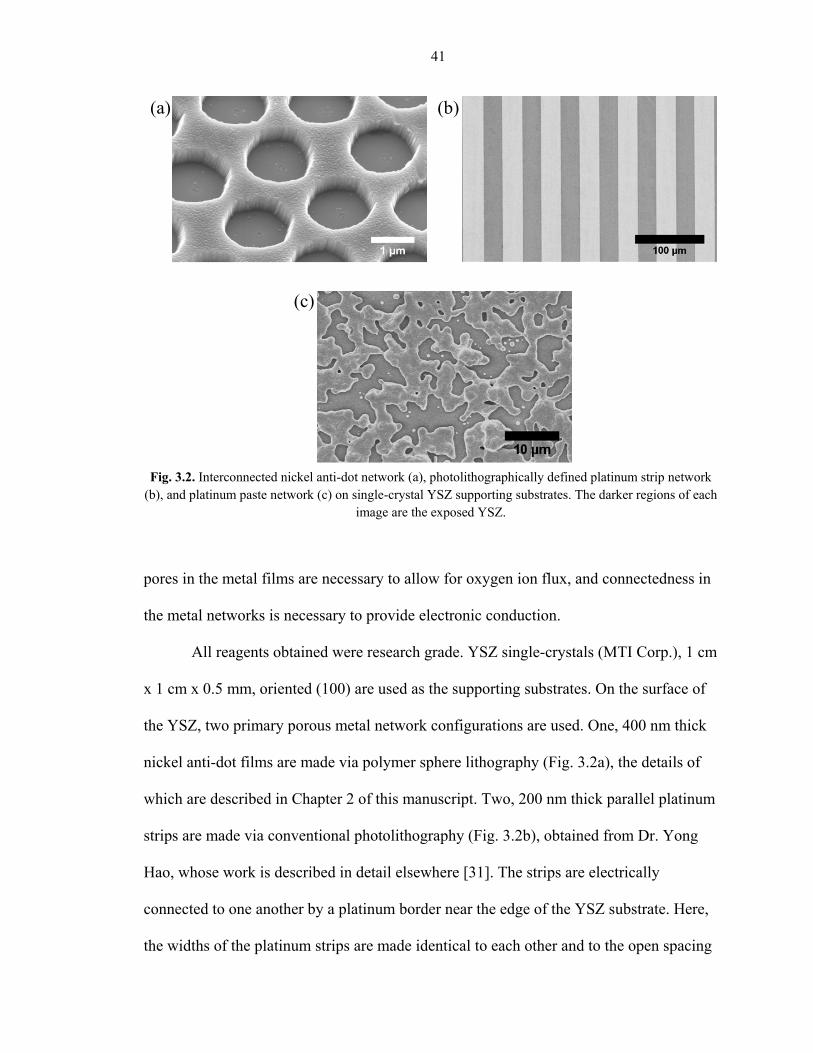
All reagents obtained were research grade. YSZ single-crystals (MTI Corp.), 1 cm
x 1 cm x 0.5 mm, oriented (100) are used as the supporting substrates. On the surface of
the YSZ, two primary porous metal network configurations are used. One, 400 nm thick
nickel anti-dot films are made via polymer sphere lithography (Fig. 3.2a), the details of
which are described in Chapter 2 of this manuscript. Two, 200 nm thick parallel platinum
strips are made via conventional photolithography (Fig. 3.2b), obtained from Dr. Yong
Hao, whose work is described in detail elsewhere [31]. The strips are electrically
connected to one another by a platinum border near the edge of the YSZ substrate. Here,
the widths of the platinum strips are made identical to each other and to the open spacing
(a)
(c)
(b)
Fig. 3.2. Interconnected nickel anti-dot network (a), photolithographically defined platinum strip network (b), and platinum paste network (c) on single-crystal YSZ supporting substrates. The darker regions of each
image are the exposed YSZ.

42
between them, denoted by the shorthand 5-5µm and 10-10µm, indicating that the widths
are 5 and 10 µm, respectively. It should be mentioned that these lithographic networks
allow both the metal and exposed YSZ surface areas to be specifically known, to a high
degree of accuracy.
One additional, thicker metal network configuration is used, but only to test the
high temperature annealing behavior of the deposits (Fig. 3.2c). Platinum paste
(Engelhard 6082) is spread across the entire YSZ surface and allowed to dry for two
hours, and then heat treated at 400 °C for 1 hour and 900 °C for 2 hours at 1 °C min-1 to
remove residual organics and sinter the platinum particles together. This results in a
spider-web-like network of platinum with feature sizes on the order of microns, necessary
to prevent metal coarsening at higher temperatures from damaging the deposits.
To obtain large amounts of the deposits for bulk studies, 0.25 mm thick nickel foil
substrates are used with depositions performed at 0.8 mA cm-2 for 1-2 hours. The
powdery deposits are subsequently scraped off of the nickel foil and gathered for
analysis. Also, in order to image cross-sections of the thin film deposits, 350 – 400 nm
thick nickel films are thermally evaporated onto 1 x 1 cm silicon substrates.
3.2.2 Experimental Setup
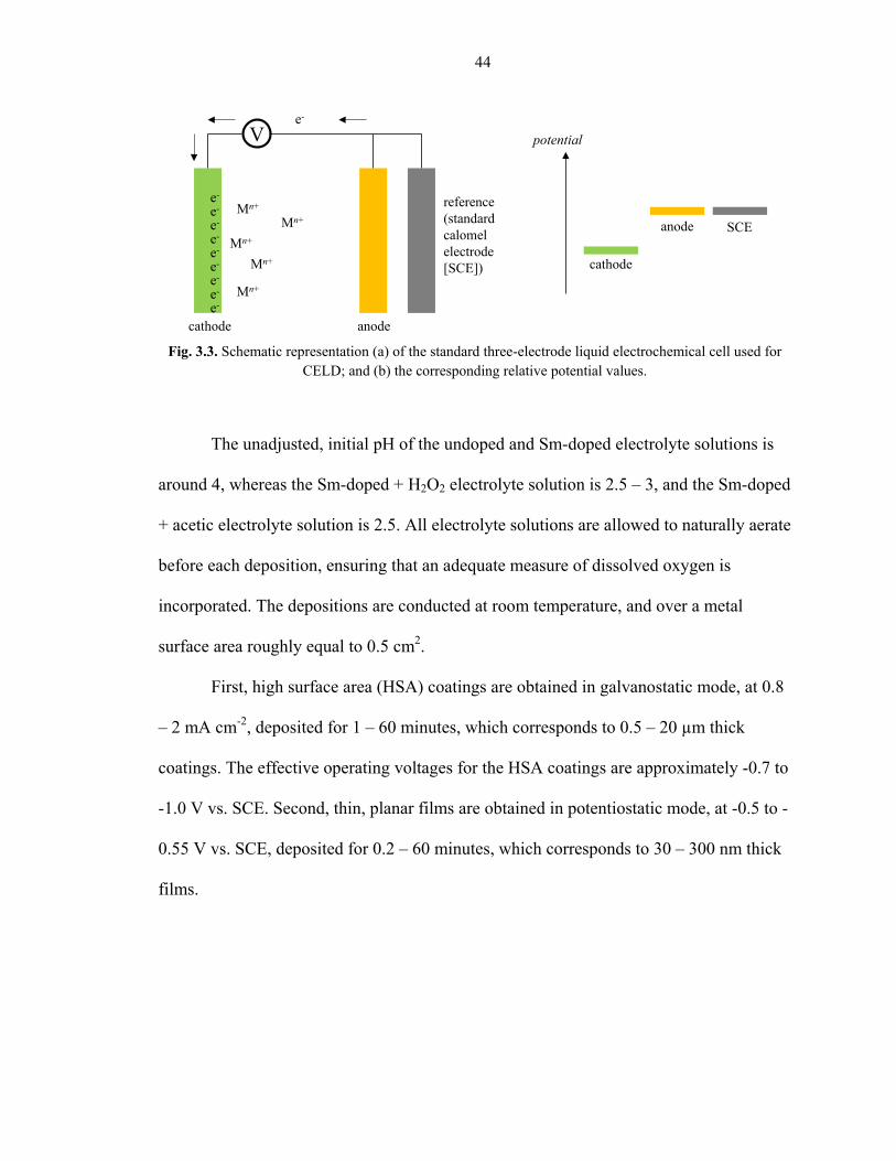
A traditional three-electrode cell, like the one schematically shown in Fig. 3.3a, is used
with a standard calomel electrode (SCE) for a reference electrode, and a carbon rod for
the counter (anodic) electrode, using a Solartron 1286 Electrochemical Interface for
potentio/galvanostatic control.
(a) (b)
43
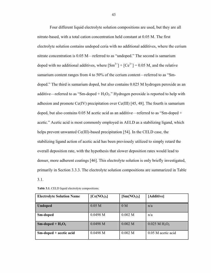
Four different liquid electrolyte solution compositions are used, but they are all
nitrate-based, with a total cation concentration held constant at 0.05 M. The first
electrolyte solution contains undoped ceria with no additional additives, where the cerium
nitrate concentration is 0.05 M—referred to as “undoped.” The second is samarium
doped with no additional additives, where [Sm3+] + [Ce3+] = 0.05 M, and the relative
samarium content ranges from 4 to 50% of the cerium content—referred to as “Sm-
doped.” The third is samarium doped, but also contains 0.025 M hydrogen peroxide as an
additive—referred to as “Sm-doped + H2O2.” Hydrogen peroxide is reported to help with
adhesion and promote Ce(IV) precipitation over Ce(III) [45, 48]. The fourth is samarium
doped, but also contains 0.05 M acetic acid as an additive—referred to as “Sm-doped +
acetic.” Acetic acid is most commonly employed in AELD as a stabilizing ligand, which
helps prevent unwanted Ce(III)-based precipitation [54]. In the CELD case, the
stabilizing ligand action of acetic acid has been previously utilized to simply retard the
overall deposition rate, with the hypothesis that slower deposition rates would lead to
denser, more adherent coatings [46]. This electrolyte solution is only briefly investigated,
primarily in Section 3.3.3. The electrolyte solution compositions are summarized in Table
3.1.
Table 3.1. CELD liquid electrolyte compositions.
Electrolyte Solution Name [Ce(NO3)3] [Sm(NO3)3] [Additive]
Undoped 0.05 M 0 M n/a
Sm-doped 0.0498 M 0.002 M n/a
Sm-doped + H2O2 0.0498 M 0.002 M 0.025 M H2O2
Sm-doped + acetic acid 0.0498 M 0.002 M 0.05 M acetic acid
44
The unadjusted, initial pH of the undoped and Sm-doped electrolyte solutions is
around 4, whereas the Sm-doped + H2O2 electrolyte solution is 2.5 – 3, and the Sm-doped
+ acetic electrolyte solution is 2.5. All electrolyte solutions are allowed to naturally aerate
before each deposition, ensuring that an adequate measure of dissolved oxygen is
incorporated. The depositions are conducted at room temperature, and over a metal
surface area roughly equal to 0.5 cm2.
First, high surface area (HSA) coatings are obtained in galvanostatic mode, at 0.8
– 2 mA cm-2, deposited for 1 – 60 minutes, which corresponds to 0.5 – 20 µm thick
coatings. The effective operating voltages for the HSA coatings are approximately -0.7 to
-1.0 V vs. SCE. Second, thin, planar films are obtained in potentiostatic mode, at -0.5 to -
0.55 V vs. SCE, deposited for 0.2 – 60 minutes, which corresponds to 30 – 300 nm thick
films.
V
cathode anode
reference (standard calomel electrode [SCE])
e-
e-
e-
e-
e-
e-
e-
e-
e-
e-Mn+
Mn+
Mn+
Mn+
Mn+
cathode
anode SCE
potential
Fig. 3.3. Schematic representation (a) of the standard three-electrode liquid electrochemical cell used for CELD; and (b) the corresponding relative potential values.
(a) (b)
45
3.2.3 Characterization Details
Both as-deposited and annealed deposits are analyzed, with typical annealing
temperatures ranging from 650 – 1000 °C for 10 – 24 hours, in 0.1% H2 in Ar, or in
ambient air. “Bulk” characterization results from deposits that are scraped off of nickel
foil substrates (not patterns), to eliminate convolution of substrate effects. These coatings
are deposited for relatively longer periods at the HSA working potential, but are identical
in every other way to their thinner counterparts. X-ray diffraction patterns (XRD) are
obtained using a Phillips X’Pert Pro powder x-ray diffractometer using Cu Kα radiation
(45 kV, 40 mA). Raman spectra are obtained with a Renishaw Ramascope (532 nm diode
pumped laser) equipped with a Leica DMLM microscope, and FT-IR spectra are obtained
using a Durascope Nicolet ATR system (KBr beam splitter). Thermogravimetric analysis
is performed with a Netzsch STA 449 C. The electrolyte solutions are characterized using
cyclic voltammetry (CV) at 50 mV s-1 from 0 to -1.25 V vs. SCE, using the same
Solartron 1286. The morphology of the coatings are imaged using scanning electron
microscopy (SEM), with two different systems, a Zeiss 1550VP FE SEM equipped with
an Oxford INCA x-ray energy dispersive spectrometer (EDS) and a Hitachi S-4100 FE
SEM. Atomic-force microscopy (AFM) is used to measure the thin, planar films’
roughness with a Park Systems XE-70. Transmission electron microscopy (TEM) is
performed on a FEI Tecnai F30UT operated at 300 kV, with the lift-out performed on an
Omniprobe Autoprobe 200 (the lift-out procedural details are summarized elsewhere)
[87-88].
46
3.3 Results
3.3.1 Bulk
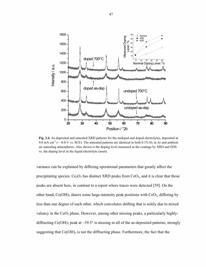
Fig. 3.4 shows the as-deposited and annealed XRD patterns for typical CELD ceria
deposits, both for the undoped and Sm-doped electrolyte solutions. These particular
deposits were obtained at 0.8 mA cm-2, approximately corresponding to -0.8 V vs. SCE
(the Sm-doped, Sm-doped + H2O2, and Sm-doped + acetic electrolyte solutions give
qualitatively identical XRD patterns). In all cases, both the as-deposited and annealed
deposit patterns show a cubic fluorite structure, indicating that CeO2-δ is the primary
phase at this working potential, regardless of the temperature history or annealing
atmosphere. Similar behavior has been observed in the literature [53, 77]. The as-
deposited patterns are shifted to slightly lower diffracting angles, indicating some level of
Ce(III) content that is afterwards oxidized to Ce(IV) upon annealing. The lattice
constants of the doped films post-annealing can be used to determine how much
samarium is incorporated into the ceria structure. The measured samarium doping levels
in the deposits are compared to the nominal samarium doping levels in the electrolyte
solution, and are plotted in the inset of Fig. 3.4. Also shown are the EDS compositional
analyses. It is evident that the concentration of samarium in the films is greater than the
concentration of samarium in the electrolyte solutions. From these results, a solution
samarium relative concentration of 4.6% is chosen in order to obtain a target deposit
composition of ~12%, which is a desirable doping level in terms of optimal oxygen ion
conductivity.
Some ambiguity in the literature exists with regard to the as-deposited crystal
structure, as both crystalline Ce2O3 and Ce(OH)3 are possibilities, although some of the
47
variance can be explained by differing operational parameters that greatly affect the
precipitating species. Ce2O3 has distinct XRD peaks from CeO2, and it is clear that those
peaks are absent here, in contrast to a report where traces were detected [59]. On the
other hand, Ce(OH)3 shares some large-intensity peak positions with CeO2, differing by
less than one degree of each other, which convolutes shifting that is solely due to mixed
valency in the CeO2 phase. However, among other missing peaks, a particularly highly-
diffracting Ce(OH)3 peak at ~39.5° is missing in all of the as-deposited patterns, strongly
suggesting that Ce(OH)3 is not the diffracting phase. Furthermore, the fact that the
20 30 40 50 60 70 80 900
200
400
600
800
1000
1200
1400
1600
1800
20 30 40 50 60 70 80 9020 30 40 50 60 70 80 90
Inte
nsity
/ a.
u.
Position / °2θ
5 10 15 20 25 30
10
20
30
40
50
60
Mea
sure
d Do
ping
Lev
el /
%
Nominal Doping Level / %
Nominal XRD EDS
undoped as-dep
undoped 700°Cdoped as-dep
doped 700°C
Fig. 3.4. As-deposited and annealed XRD patterns for the undoped and doped electrolytes, deposited at 0.8 mA cm-2 (~ -0.8 V vs. SCE). The annealed patterns are identical in both 0.1% H2 in Ar and ambient air annealing atmospheres. Also shown is the doping level measured in the coatings by XRD and EDS vs. the doping level in the liquid electrolyte (inset).
48
0.0 0.1 0.2 0.30
10
20
30
HWHM
/ cm
-1
d-1 / nm-1
Saitzek 2008 Weber 1993 Kosacki 2002 HWHM Lorentz
3000 3500 40000.00
0.05
0.10
0.15
0.20
1000°C anneal
as-dep
700°C anneal
Inte
nsity
/ a.
u.
Wavenumber / cm-1
250 500 750 1000 12500.0
0.5
1.0
1.5
2.0
2.5
Inte
nsity
/ a.
u.
Wavenumber / cm-1
doped +
H2O2
undoped
doped
nitrate ionsoxygenvacancies
Ce-O8 stretching mode
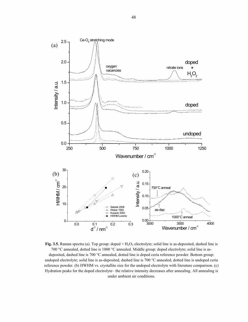
Fig. 3.5. Raman spectra (a). Top group: doped + H2O2 electrolyte; solid line is as-deposited, dashed line is 700 °C annealed, dotted line is 1000 °C annealed. Middle group: doped electrolyte; solid line is as-
deposited, dashed line is 700 °C annealed, dotted line is doped ceria reference powder. Bottom group: undoped electrolyte; solid line is as-deposited, dashed line is 700 °C annealed, dotted line is undoped ceria reference powder. (b) HWHM vs. crystallite size for the undoped electrolyte with literature comparison. (c) Hydration peaks for the doped electrolyte– the relative intensity decreases after annealing. All annealing is
under ambient air conditions.
(a)
(c) (b)

49
annealed patterns are simply shifted versions of their as-deposited counterparts reinforces
this notion.
The as-deposited peaks are broader than the annealed peaks in every case,
indicating grain growth at high temperatures. Using the general Scherrer equation (D =
0.9λ/βcosθ), where D is the crystallite size, λ is the x-ray wavelength, β is the adjusted
full-width half max of the peak at position 2θ, the as-deposited crystallite size is
determined to be approximately 6 nm, which increases to 15 – 20 nm after annealing at
700 °C for 10 hours in either reducing or oxidizing atmospheres. This is in good
agreement with others’ CELD of ceria findings [78, 83]. The undoped results are
summarized in Fig. 3.5b, where the half-width at half-max of the Raman peak at ~466
cm-1 is plotted against the inverse of the crystallite size. The sizes obtained in this work
even correspond well with undoped ceria obtained by other fabrication means [89-91].
Fig. 3.5a shows the Raman spectra obtained for all three electrolyte solutions as-
deposited and annealed at 700 °C, as well as undoped and Sm-doped reference spectra,
and one scan of a Sm-doped + H2O2 sample annealed at 1000 °C. All of the spectra share
a main Ce-O stretching mode peak centered at ~466 cm-1 [89-91], which shifts upon
samarium doping [46, 50]. As can be seen, the annealed undoped and Sm-doped main
peaks agree well with their respective references. This band can also reportedly shift up
to ~10 wavenumbers due to nanoscale crystallite size effects [58, 91-92], which could
partly explain why the Sm-doped and Sm-doped + H2O2 as-deposited peaks are shifted
from one another. The exact doping level in the deposits could also be slightly different
for these two electrolyte solutions. A band at ~600 cm-1 indicates oxygen vacancies in the
ceria lattice [46], which is seen in all of the Sm-doped and Sm-doped + H2O2 scans, as

50
well as the as-deposited undoped sample. The origin of this peak is the samarium doping
in the Sm-doped electrolyte solutions’ cases, and partial Ce(III) content in the as-
deposited undoped case, whose peak disappears upon annealing. These data agree well
with the XRD results. Also, oxygen vacancies have been known to shift the main Ce-O
peak, perhaps explaining the lack of movement from as-deposited to annealed samples
with the Sm-doped electrolyte solution. The bands centered at ~740 and 1049 cm-1 are
attributed to nitrate ions [53], and they disappear upon annealing, as expected.
In the 3000 – 4000 cm-1 range, a broad multi-peak exists for all of the electrolyte
solutions’ as-deposited samples, depicted for the Sm-doped electrolyte solution in Fig.
3.5c. A peak in this range indicates some O-H inclusion in the deposit, either as H2O or
hydroxides. The distinction between the two, particularly for xH2O·CeO2 and Ce(OH)4 is
subtle [56, 92], and unimportant for the ultimate aim of this work. What this peak does
indicate, however, is that there is some hydrated content in the as-deposited samples,
even though the XRD patterns exhibit the cubic fluorite structure. After annealing to 700
°C, these Raman peaks decrease in relative intensity and appear to reach a steady-state,
possibly indicating some grain boundary and/or unavoidable powder surface hydration.
Selected FT-IR spectra are shown in Fig. 3.6. All depositions give qualitatively
identical spectra, so only the Sm-doped case is shown. These results show further
evidence of hydration of the as-deposited material. The as-deposited scan (Fig. 3.6a)
exhibits two peaks attributed to OH stretching (~3600 cm-1, broad) and bending (~1640
cm-1, sharp) modes, that are shared with liquid water, shown for reference in Fig. 3.6 as
the dotted line. Additionally, carbonate (~1450 cm-1) and nitrate (~1300 and 1040 cm-1)
peaks are identified [53]. Fig. 3.6c and 3.6d are spectra from Sm-doped deposits annealed
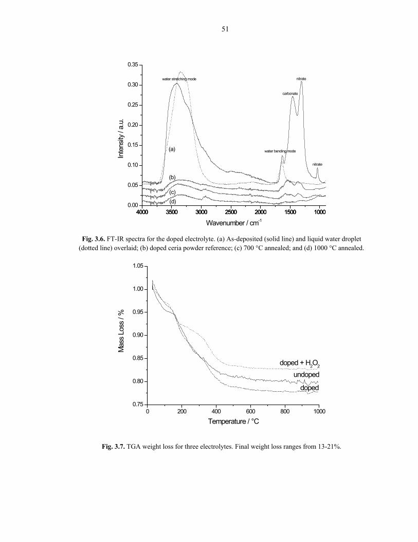
51
4000 3500 3000 2500 2000 1500 10004000 3500 3000 2500 2000 1500 10000.00
0.05
0.10
0.15
0.20
0.25
0.30
0.35
4000 3500 3000 2500 2000 1500 1000
(d)(c)
(b)
(a)
nitrate
nitrate
carbonate
water bending mode
water stretching mode
Wavenumber / cm-1
Inte
nsity
/ a.
u.
0 200 400 600 800 10000.75
0.80
0.85
0.90
0.95
1.00
1.05
doped
doped + H2O2
undoped
Mas
s Lo
ss /
%
Temperature / °C
Fig. 3.6. FT-IR spectra for the doped electrolyte. (a) As-deposited (solid line) and liquid water droplet (dotted line) overlaid; (b) doped ceria powder reference; (c) 700 °C annealed; and (d) 1000 °C annealed.
Fig. 3.7. TGA weight loss for three electrolytes. Final weight loss ranges from 13-21%.
52
at 700 and 1000 °C, respectively, showing all peaks dramatically losing intensity,
consistent with the XRD and Raman results. The spectra from the annealed deposits
correlate well with a SDC reference spectrum (Fig. 3.6b). TGA measurements underscore
these data, showing significant weight loss (~13-21%) upon heating (Fig. 3.7) [48, 78].
From the previous results, this is probably due to a combination of hydration, nitrate, and
carbonate removal.
3.3.2 High Surface Area (HSA) Coatings
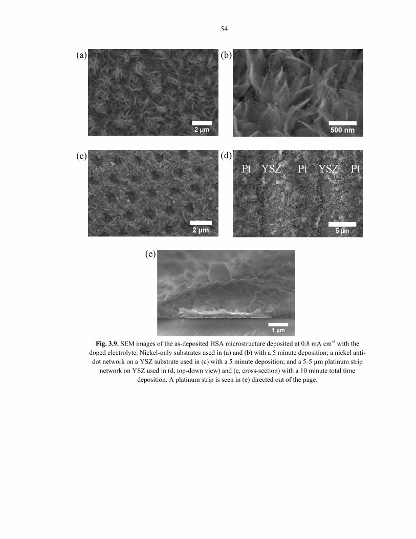
Fig. 3.8 and Fig. 3.9 show representative SEM images of a HSA coating deposited at 0.8
mA cm-2 on various substrates with the undoped and Sm-doped electrolyte solutions,
respectively. The microstructure appears to consist of an overlapping, intersecting
combination of needle-like and nano-sheet growth emerging from the substrate base, with
widths varying from 10 – 50+ nm. Similar microstructures have been reported in refs [46,
53, 77, 80]. There is a slight morphological change between the undoped and Sm-doped
electrolyte solutions, as can be seen by comparing Figures 3.8 and 3.9, but is minimal
compared to the difference toggled by changing the depositing potential. The coating
thickness depends on the deposition time, but typically ranges from slightly less than 1
µm up to tens of microns.
The operational current density was found to alter the overall morphology and,
particularly, the sizes of the finer features, with 0.8 mA cm-2 being the most ideal current
density because of its large-scale deposition uniformity and its nanoscale features.
Extensive SEM analysis of the deposits obtained from a variety of experimental
conditions revealed that smaller current densities tend toward lower surface area,
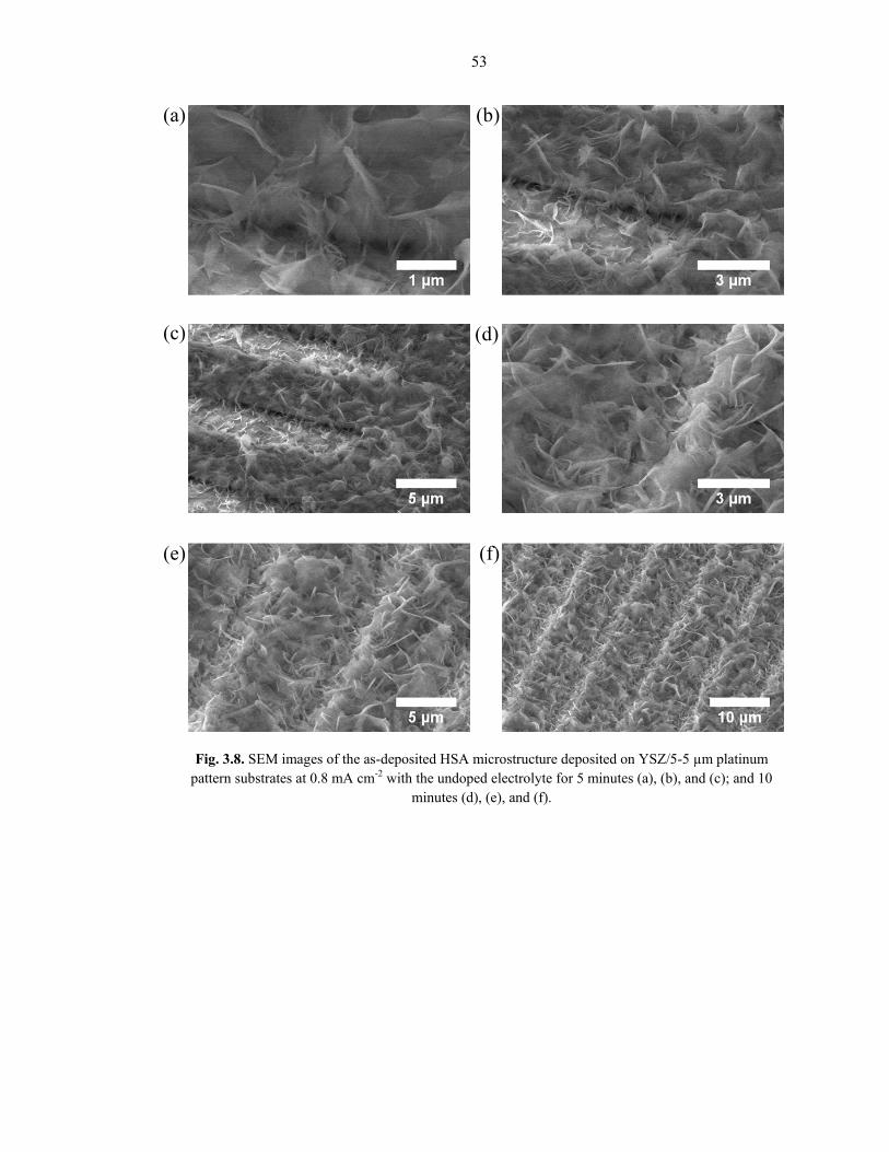
53
Fig. 3.8. SEM images of the as-deposited HSA microstructure deposited on YSZ/5-5 µm platinum pattern substrates at 0.8 mA cm-2 with the undoped electrolyte for 5 minutes (a), (b), and (c); and 10
minutes (d), (e), and (f).
(a) (b)
(c) (d)
(e) (f)
(a) (b)
(c) (d)
(e) (f)
54
Fig. 3.9. SEM images of the as-deposited HSA microstructure deposited at 0.8 mA cm-2 with the doped electrolyte. Nickel-only substrates used in (a) and (b) with a 5 minute deposition; a nickel anti-dot network on a YSZ substrate used in (c) with a 5 minute deposition; and a 5-5 µm platinum strip
network on YSZ used in (d, top-down view) and (e, cross-section) with a 10 minute total time deposition. A platinum strip is seen in (e) directed out of the page.
(a) (b)
(c) (d)
(e)

55
featureless coatings, and larger current densities tend to encourage different growth rates
in different depositing areas, producing bush-like regions at the expense of less
developed regions. 0.8 mA cm-2 approximately corresponds to -0.8 V vs. SCE;
alternatively, these microstructures can be fabricated potentiostatically, but galvanostatic
mode is more consistent run-to-run for the HSA morphology. Despite the fairly
randomized nanoscale features, the deposition is ubiquitous and uniform, even up to
several cm2. The morphology evolves from nicely adherent to largely cracked as the
deposition time and, hence, coating thickness increase. The HSA microstructure is
maintained, even when metal network substrates are used (c.f. Fig. 3.8, 3.9c, d, and e).
An analogous, but not identical HSA morphology can be obtained using the Sm-
Fig. 3.10. SEM images of the as-deposited HSA microstructure obtained with the doped + H2O2 electrolyte at 0.8 mA cm-2.
(a) (b)
(c) (d)

56
doped + H2O2 electrolyte solution, shown in Fig. 3.10, but the finer features are larger in
size and fewer in number than the Sm-doped electrolyte solution and thereby less ideal
for surface area enhancement. The HSA structure was not attempted for the Sm-doped +
acetic electrolyte solution, as the acetic acid addition is intended for dense, thin film
growth.
To probe the high temperature stability of the HSA microstructure, HSA
deposition was performed on platinum paste substrates (c.f. Fig. 3.2c), and subsequently
annealed at temperatures of 800, 1000, and 1100 °C (Fig. 3.11a, b, and c, respectively)
for 10 hours in ambient air. As can be seen, the nanoscale features stay intact up to 800
°C, at which temperature some coarsening begins and then worsens as the temperature
Fig. 3.11. Doped electrolyte HSA morphology high temperature stability with platinum paste networks on YSZ substrates: (a) annealed for 10 hours in ambient air at 800 °C; (b) 1000 °C; and (c) 1100 °C. Also,
cracks can form after annealing, shown in (d) for the doped electrolyte on a YSZ/nickel anti-dot substrate, but are healed by a subsequent deposition (d, inset).
(a) (b)
(c) (d)
57
increases up to 1100 °C, at which point the finer features have nearly coarsened away.
This coarsening behavior is reasonable, considering the melting temperature of ceria is
~2400 °C. Although not always the case, some microscale shrinkage that leads to
significant cracking can occur even after lower temperature annealing, i.e., 650 – 700 °C
(Fig. 3.11d). This problem is particularly pronounced for thicker coatings. However,
subsequent depositions can heal cracks that have formed, at least as far as the SEM can
image, as shown in the inset of Figure 3.11d. Additionally, for relatively thick coatings,
the microstructure can emerge from the electrolyte solution cracked as-deposited, even
before any heat treatment—without exception, previous studies on the HSA
microstructure only report cracked as-deposited coatings [46, 53, 77, 80]. It is unclear
whether this cracking is due to drying, or the deposition process itself. For both the
deposition-related and annealing-related cracking issues, the comparatively thinner, more
conformal depositions on porous metal networks on YSZ are more resistant to cracking
than metal-only substrates. The in-plane degrees of freedom of the porous metal networks
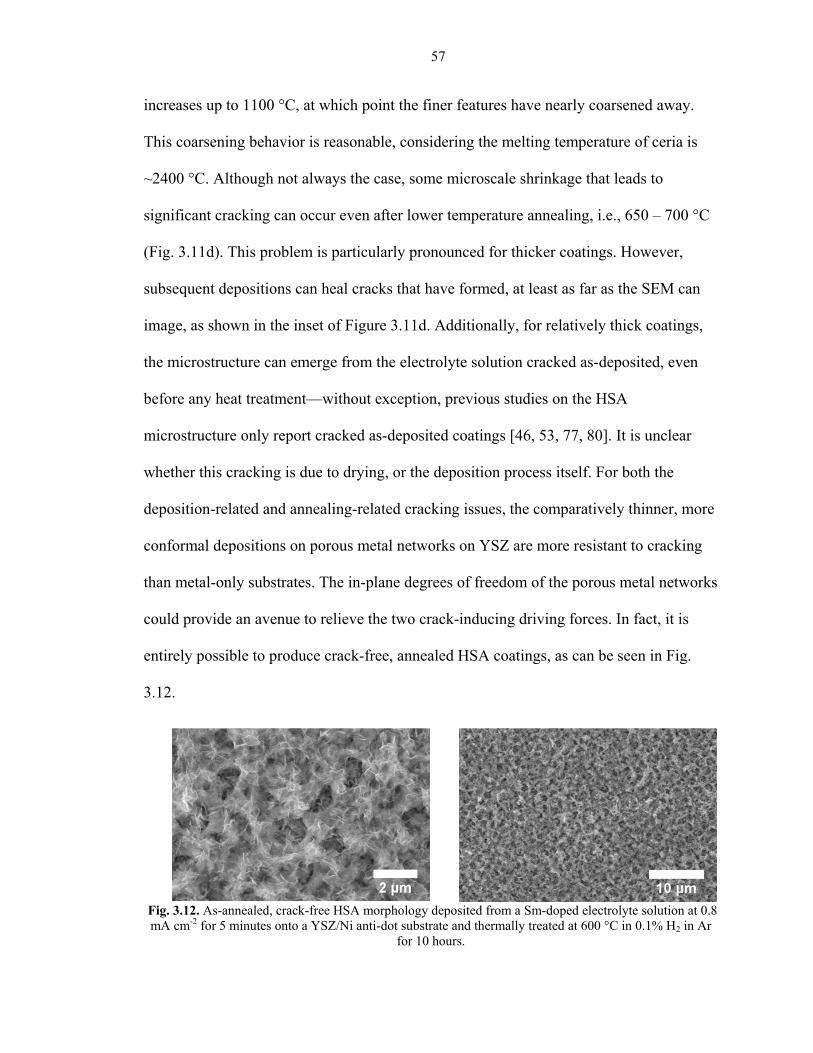
could provide an avenue to relieve the two crack-inducing driving forces. In fact, it is
entirely possible to produce crack-free, annealed HSA coatings, as can be seen in Fig.
3.12.
Fig. 3.12. As-annealed, crack-free HSA morphology deposited from a Sm-doped electrolyte solution at 0.8 mA cm-2 for 5 minutes onto a YSZ/Ni anti-dot substrate and thermally treated at 600 °C in 0.1% H2 in Ar
for 10 hours.

58
3.3.3 Thin Films
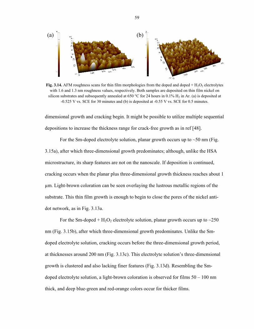
Planar, thin films were obtained potentiostatically at operating voltages from -0.5 to -0.55
V vs. SCE. These films are practically featureless, as in Fig. 3.13b, and nearly atomically
smooth—even after annealing at 650 °C for 24 hours in 0.1% H2 in Ar, the average
surface roughness measured by AFM is 1.6 nm for the Sm-doped electrolyte solution and
1.3 nm for the Sm-doped + H2O2 electrolyte solution (Fig. 3.14). For all four electrolyte
solutions, crack-free, planar growth occurs up to a point, when undesirable three-
Fig. 3.13. As-deposited thin film morphologies. (a) Doped electrolyte (deposited at -0.525 V vs. SCE), highly magnified view of the thin film deposit closing a pore of the nickel anti-dot network; (b) top-down view of the characteristically featureless doped + H2O2 electrolyte thin film; (c) cracks form
at thicknesses above 200 nm with the doped + H2O2 electrolyte; (d) globular, three-dimensional growth occurs at thicknesses above 250 nm with the doped + H2O2 electrolyte. The samples in (b) –
(d) are deposited at an applied potential of -0.55 V vs. SCE.
(a) (b)
(c) (d)
59
dimensional growth and cracking begin. It might be possible to utilize multiple sequential
depositions to increase the thickness range for crack-free growth as in ref [48].
For the Sm-doped electrolyte solution, planar growth occurs up to ~50 nm (Fig.
3.15a), after which three-dimensional growth predominates; although, unlike the HSA
microstructure, its sharp features are not on the nanoscale. If deposition is continued,
cracking occurs when the planar plus three-dimensional growth thickness reaches about 1
µm. Light-brown coloration can be seen overlaying the lustrous metallic regions of the
substrate. This thin film growth is enough to begin to close the pores of the nickel anti-
dot network, as in Fig. 3.13a.
For the Sm-doped + H2O2 electrolyte solution, planar growth occurs up to ~250
nm (Fig. 3.15b), after which three-dimensional growth predominates. Unlike the Sm-
doped electrolyte solution, cracking occurs before the three-dimensional growth period,
at thicknesses around 200 nm (Fig. 3.13c). This electrolyte solution’s three-dimensional
growth is clustered and also lacking finer features (Fig. 3.13d). Resembling the Sm-
doped electrolyte solution, a light-brown coloration is observed for films 50 – 100 nm
thick, and deep blue-green and red-orange colors occur for thicker films.
Fig. 3.14. AFM roughness scans for thin film morphologies from the doped and doped + H2O2 electrolytes with 1.6 and 1.3 nm roughness values, respectively. Both samples are deposited on thin film nickel on
silicon substrates and subsequently annealed at 650 °C for 24 hours in 0.1% H2 in Ar. (a) is deposited at -0.525 V vs. SCE for 30 minutes and (b) is deposited at -0.55 V vs. SCE for 0.5 minutes.
(a) (b)

60
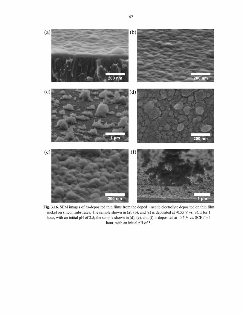
The Sm-doped + acetic electrolyte solution yields deposits very similar to the Sm-
doped electrolyte solution (see Fig. 3.16ab). This electrolyte solution poses some
difficulty in maintaining uniform two-dimensional growth across the entirety of the
substrate, however. As an example, Fig. 3.16c is shown, which is an image taken from
the same sample as in Fig. 3.16a and b. Although limited to a few trials, adjusting the
initial pH by NaOH addition significantly alters the deposited morphology, as can be seen
in Fig. 3.16d, e, and f for an initial pH adjusted from 2.5 to 5. With higher pH, rounded,
gumdrop-like islands nucleate and grow, although it is unclear if they are completely
connected, and there are uncontrollable sections of three-dimensional growth.
Sm-doped + H2O2 ceria-coated platinum strips are shown as-deposited (Fig.
3.17a) and annealed in 0.1% H2 in Ar (Fig. 3.17b). Practically no distinction can be made
via SEM before and after annealing. Fig. 3.17c shows two platinum strips after annealing,
where the left strip is coated and the right is uncoated. Significant surface roughness
differences can be seen between the two, noting that the exposed platinum has begun to
coarsen, whereas the coated platinum appears to be physically prevented from doing so.
That neither the as-deposited nor the annealed films are cracked is consistent with a
Fig. 3.15. SEM images of as-deposited thin film cross sections deposited on thin film nickel on silicon substrates from (a) the doped electrolyte at -0.5 V vs. SCE for 1 hour, with a thickness of ~40 nm (image
taken at a 75° angle); and (b) the doped + H2O2 electrolyte at -0.55 V vs. SCE for 5 minutes, with a thickness of ~200 nm (image taken at a 90° angle).
(a) (b)

61
report that defined a critical crystallite size of 28 nm, via XRD determination, only above
which cracking in thin ceria films occur, albeit for anodic depositions [93]. From the
XRD analysis above, the as-deposited and annealed crystallite sizes in this work are
below this critical value.
To summarize the CELD findings thus far, depositing conditions were identified
that produced both HSA and thin, planar film morphologies, across a variety of
electrolyte solution compositions. It appears as though an additive-free electrolyte
solution maximizes the apparent surface area for the HSA deposits. Also, hydrogen
peroxide allows thicker films to be deposited, as compared to the additive-free Sm-doped
electrolyte solution. In all cases and for each morphology, there is no discernable
microstructural evolution at fuel cell operating temperatures. Desirable levels of
samarium doping have also been incorporated into the deposits.
62
Fig. 3.16. SEM images of as-deposited thin films from the doped + acetic electrolyte deposited on thin film nickel on silicon substrates. The sample shown in (a), (b), and (c) is deposited at -0.55 V vs. SCE for 1 hour, with an initial pH of 2.5; the sample shown in (d), (e), and (f) is deposited at -0.5 V vs. SCE for 1
hour, with an initial pH of 5.
(a) (b)
(c) (d)
(e) (f)

63
Fig. 3.17. Three SEM images taken from the same platinum strip on YSZ sample, with a thin ceria coating deposited from the doped + H2O2 electrolyte at -0.55 V vs. SCE for 0.5 minutes: (a) as-deposited, coated platinum strip before annealing; (b) a coated platinum strip after annealing at 650 °C for 24 hours in 0.1%
H2 in Ar, with no discernable microstructural evolution of the coating or the platinum; (c) different coarsening behavior is observed for coated (c, left) and uncoated (c, right) platinum strips after annealing.
Identical results are observed for the doped electrolyte as well.
(a) (b)
(c)
64
3.4 Discussion
3.4.1 General Deposition Overview
Recall from Section 1.4.2 that the CELD of ceria via electrogeneration of base proceeds
in two distinct steps—electrochemical reduction of electrolyte solution species, and
subsequent chemical precipitation of cerium species. Note: Ce3+/4+ herein specifically
refers to dissociated aqueous ions, whereas Ce(III/IV) refers to precipitated/solid species
of a particular cerium valence state.
During the electrochemical reduction step, either acidic species are consumed or
basic species are produced, and both quickly increase the interfacial pH. The primary
species that are reduced are dissolved oxygen, hydronium ions, water, nitrate ions, and
hydrogen peroxide (if present) [80, 86]. Although not exhaustive, the following list of
equations describes their reduction behavior:
𝑂2 + 2𝐻2𝑂 + 4𝑒− → 4𝑂𝐻− (3.1)
𝑂2 + 2𝐻2𝑂 + 2𝑒− → 2𝑂𝐻− + 𝐻2𝑂2 (3.2)
2𝐻3𝑂+ + 2𝑒− → 𝐻2 + 2𝐻2𝑂 (3.3)
2𝐻2𝑂 + 2𝑒− → 𝐻2 + 2𝑂𝐻− (3.4)
𝑁𝑂3− + 7𝐻2𝑂 + 8𝑒− → 𝑁𝐻4+ + 10𝑂𝐻− (3.5)
𝑁𝑂3− + 𝐻2𝑂 + 2𝑒− → 𝑁𝑂2− + 2𝑂𝐻− (3.6)
𝐻2𝑂2 + 2𝑒− → 2𝑂𝐻− (3.7)
As an applied cathodic potential is made more negative, interfacial pH values
measured in situ increase to and stabilize at ~10.5 at around -0.4 V vs. SCE, until the
potential reaches -1.0 V vs. SCE, at which point the pH jumps upwards of 12 [86]. This
corresponds well with calculated interfacial pH values in the range of 10.5 – 10.8 at -0.85
V vs. SCE [82]. Addition of nitrate ions to the electrolyte solution only affect the pH
values at potentials more negative than -1.0 V vs. SCE [86], outside of the operational
65
range for this work; therefore, the effect of nitrate ions on the pH can be disregarded.
Note that for all of these reductions, available electrons are required at the surface of the
cathode in order for base to continue to be electrogenerated.
Once the electrolyte solution has become sufficiently basic, or, equivalently,
enough hydroxide ions have been produced, chemical precipitation begins. There are two
precipitation pathways thought to occur. The first is through Ce(III) (Eqn. 3.8), and the
second is through Ce(IV) species, but only if H2O2 is present (Eqn. 3.9-3.11):
𝐶𝑒3+ + 3𝑂𝐻− → 𝐶𝑒(𝑂𝐻)3 (3.8)
2𝐶𝑒3+ + 2𝑂𝐻− + 𝐻2𝑂2 → 2𝐶𝑒(𝑂𝐻)22+ (3.9)
𝐶𝑒(𝑂𝐻)22+ + 2𝑂𝐻− → 𝐶𝑒(𝑂𝐻)4 ↓ (3.10)
𝐶𝑒(𝑂𝐻)22+ + 2𝑂𝐻− → 2𝐻2𝑂 + 𝐶𝑒𝑂2 ↓ (3.11)
If Ce(III/IV) hydroxides are the precipitating species, they are readily oxidized to CeO2 in
the presence of O2:
4𝐶𝑒(𝑂𝐻)3 + 𝑂2 → 4𝐶𝑒𝑂2 + 6𝐻2𝑂 (3.12)
𝐶𝑒(𝑂𝐻)4𝑂2�� 𝐶𝑒𝑂2 + 2𝐻2𝑂 (3.13)
Recognizing that naturally aerated electrolyte solution s contain a non-trivial amount of
dissolved oxygen, these chemical oxidations can proceed to CeO2 at any point during the
deposition, and definitively occur once the deposit is taken out of the liquid electrolyte
and exposed to the ambient air. The previous XRD and Raman results suggest that this
oxidation process is fast, even at room temperature. This explains how, even for
conditions that should yield strictly Ce(III) precipitation, some Ce(IV) is detected in situ
via XANES [82].
The Pourbaix diagram from Fig. 3.1. is a helpful aid to understand which cerium
species are involved during the chemical precipitation step. As can be seen in the

66
diagram, for most pH values and mild potentials, Ce3+ is the predominant ion in solution.
Recall that the initial state of the solution is with no applied potential and at a pH in the
range 2.5 – 4. As the state of the system moves to the right of the diagram, meaning that
the electrolyte solution is becoming more basic, stability lines are crossed, which
specifically indicates which species are involved in the precipitation step.
Consider the case for the additive-free undoped and Sm-doped electrolyte
solutions. As a reminder, the black arrow on the right-hand side vertical axis of Fig. 3.1
shows the working cathodic potential for the HSA coatings. As the electrochemical
reduction reactions proceed and the interfacial pH increases, it is clearly seen that the
Ce3+|Ce(OH)3 stability line is crossed, described by Eqn. 3.8. Intermediates of the type
𝐶𝑒(𝑂𝐻)𝑥+(3−𝑥) exist, where x ranges from 0 to 2, but reported precipitation tests
concluded that the kinetics are fast and continuous in progressing from Ce3+ to Ce(OH)3
[84]. The final pH is around 10.5, at which point Ce(OH)3 is no longer aqueous, but
precipitates out of solution. The gray arrow in Fig. 3.1 indicates the working cathodic
potential for thin films in the undoped and Sm-doped electrolyte solutions. Similar to the
HSA working potential, the Ce3+|Ce(OH)3 stability line is crossed, indicating that
Ce(OH)3 is the stable precipitating species for both morphologies in electrolyte solutions
where H2O2 is not explicitly added.
The addition of hydrogen peroxide to the electrolyte solution greatly influences its
chemistry, in particular by chemically inducing the formation of Ce(IV) aqueous species
before any potential is applied, according to Eqn. 3.9. This is observed experimentally,
manifest by the electrolyte solution appearance changing from transparent to slightly
yellow, which is a characteristic color of the Ce4+ valence state. Similarly to the above
67
discussion, Ce4+ intermediates exist of the type 𝐶𝑒(𝑂𝐻)𝑥+(4−𝑥), where x ranges from 0 to
3, but, compared to 𝐶𝑒(𝑂𝐻)2+2, the others are either thermodynamically unfavorable in
the pH range above 2.5, or kinetically unfavorable shown by precipitation tests [84-85].
Once the requisite hydroxide ions are produced, Ce(IV) precipitates form according to
either Eqn. 3.10 or 3.11. As mentioned previously, the difference between small
crystallites of xH2O·CeO2 and Ce(OH)4 is minor, especially considering that the
oxidation reaction of Ce(OH)4 to CeO2 (Eqn. 3.13) is spontaneous and sufficiently fast,
according to the XRD results in Section 3.3.1, which unambiguously show the final
crystal structure to be that of cubic fluorite CeO2.
One other H2O2-related pathway to precipitation is possible, where Ce3+ ions are
directly oxidized to Ce(IV) precipitates, without the 𝐶𝑒(𝑂𝐻)2+2 intermediate, according
to:
2𝐶𝑒3+ + 𝐻2𝑂2 + 6𝑂𝐻− → 2𝐶𝑒(𝑂𝐻)4 ↓ (3.14)
2𝐶𝑒3+ + 𝐻2𝑂2 + 6𝑂𝐻− → 4𝐻2𝑂 + 2𝐶𝑒𝑂2 ↓ (3.15)
Considering the number of species involved in these reactions, however, this scheme
seems less kinetically likely than the intermediate-involved pathway proposed above.
Either precipitation mechanism involving hydrogen peroxide can be understood in light
of the Pourbaix diagram by recognizing that hydrogen peroxide increases the effective
solution potential, changing the initial and final potential-pH states of the system [84].
One must also consider the in situ production of hydrogen peroxide via the
electrochemical reduction of dissolved oxygen through the two-electron pathway (Eqn.
3.2). Consequently, some of the produced Ce(IV) species will have been the result of the
𝐶𝑒(𝑂𝐻)2+2 path discussed above, even in nominally non-H2O2 electrolyte solutions.
68
However, given that the concentration of dissolved oxygen is on the order of µM [82],
the effect on the morphology should be much less than when mM of hydrogen peroxide
is explicitly added.
In order to further distinguish between the electrochemistries of the Sm-doped
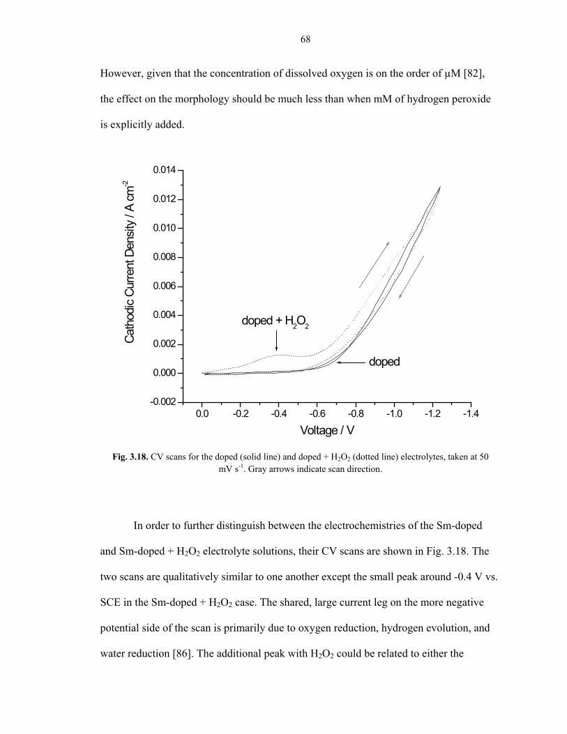
and Sm-doped + H2O2 electrolyte solutions, their CV scans are shown in Fig. 3.18. The
two scans are qualitatively similar to one another except the small peak around -0.4 V vs.
SCE in the Sm-doped + H2O2 case. The shared, large current leg on the more negative
potential side of the scan is primarily due to oxygen reduction, hydrogen evolution, and
water reduction [86]. The additional peak with H2O2 could be related to either the
0.0 -0.2 -0.4 -0.6 -0.8 -1.0 -1.2 -1.4-0.002
0.000
0.002
0.004
0.006
0.008
0.010
0.012
0.014
doped
doped + H2O2
Cath
odic
Curre
nt D
ensit
y / A
cm
-2
Voltage / V
Fig. 3.18. CV scans for the doped (solid line) and doped + H2O2 (dotted line) electrolytes, taken at 50 mV s-1. Gray arrows indicate scan direction.
69
reduction of H2O2 itself (Eqn. 3.7), or the reduction of Ce(IV) species that had been
previously oxidized by H2O2. Using KNO3 + H2O2 as a reference electrolyte solution
without any cerium species, the resulting CV scan exhibits no additional peak (not
shown), indicating that its presence is related to the cerium species. Therefore, the peak’s
likely origin is an electrochemical reduction of the type:
𝐶𝑒(𝑂𝐻)22+ + 𝑒− → 𝐶𝑒3+ + 2𝑂𝐻− (3.16)
The hysteresis associated with this peak is related to the deposition that occurs
during the more negative section of the scan, which covers the electrode. The fact that
there is no additional peak observed in the Sm-doped electrolyte solution CV even after
multiple scans reinforces the notion that, although there is some in situ H2O2 production
via the reduction of dissolved oxygen, the amount is small enough to not impact the
chemistry; otherwise, an additional peak would be observed in the Sm-doped electrolyte
solution eventually.
3.4.2 The Physical Deposition Picture
A fundamental question remains unanswered. How does deposition of an insulating metal
oxide (as CeO2 is under these conditions) continue after an initial film is formed? To
address this issue, the following argument is presented.
Recall that electrons are needed at the cathode surface to reduce the various
available species, producing hydroxide ions. For 0.8 mA cm-2 at -0.8 V vs. SCE through a
100 nm film, an electronic conductivity of 10-8 Ω-1 cm-1 is required. Using the room
temperature mobility for electrons in undoped CeO2 [94], ~10-8 cm2 V-1 s-1, this gives an
electron concentration of ~1017 cm-3. However, using thermodynamic data to calculate

70
the electron concentration of undoped CeO2 at room temperature [32], a value of ~10-26
cm-3 is obtained, far below what is needed. Therefore, neither CeO2, nor the non-
conducting Ce(OH)3/Ce(OH)4 are electronically conducting enough to facilitate continual
CELD. Consequently, the deposit must remain somewhat porous throughout, constantly
allowing molecular access to the metal|electrolyte solution interface, where the requisite
electroreductions occur. A 65% dense CeO2 thin film is reported on Hastelloy substrates
measured by ellipsometry and x-ray reflectivity, although the deposition was anodic [54].
Also, cathodically-produced CeO2 nanotubes in the aligned pores of an anodic alumina
template showed small cracks and holes by TEM and SEM, particularly in areas furthest
from the working electrode [49]. In the case of highly-cracked coatings deposited over
lengthy times, there will be even easier access to the metal|electrolyte solution
interface—this allows the observed growth up to and even beyond 20 µm thick, although
there will be a reasonable thickness limitation before spallation occurs.
Building this physical deposition picture up to the nano-/microscale gives
explanation to the clear morphological difference seen in the HSA coatings and thin film
microstructures, as well as trends in the Sm-doped and Sm-doped + H2O2 electrolyte
solutions. The former is related to the rate of base electrogeneration, which is dictated by
the applied potential—faster rates (more negative potentials) encourage the HSA
morphology (Fig. 3.9 and 3.8) and slower rates (less negative potentials) encourage thin
film growth (Fig. 3.13 and 3.15). Regardless of applied potential, the Sm-doped
electrolyte solution promotes sharper featured growth, whereas the Sm-doped + H2O2
electrolyte solution generally promotes more spherical, globular growth. This is related to
the difference in precipitating species for the two electrolyte solutions—Ce(OH)3 and

71
Ce(IV) species, respectively. Hydrogen bonding between as-produced Ce(OH)3
molecules is thought to emphasize elongated, needle-like growth, in stark contrast to the
spherical growth of the CeO2 phase [53, 77, 95]. This could explain the origin of the HSA
morphology, and why the Sm-doped + H2O2 electrolyte solution has a more difficult time
producing comparatively fine nanoscale features at standard HSA working potentials. A
counter theory for the HSA morphology asserts that hydrogen evolution during the
deposition acts as a dynamic template [83]. However, at HSA depositing potentials (-0.7
to -1.0 V vs. SCE), a non-trivial amount of hydrogen evolution is visually apparent for
the platinum-based substrates, but none is observed for the nickel-based substrates. This
suggests that hydrogen evolution is not the origin of the HSA microstructure, as deposits
from both platinum and nickel exhibit the same general features.
3.4.3 Deposition on Non-Conducting Parts of the Substrate
Up to this point, it has been shown that CELD consistently produces undoped and Sm-
doped CeO2 in a predictable fashion; that both HSA and thin film morphologies are stable
at high temperatures; and that the wide parameter space allows for CELD microstructural
tunability. In surveying the fabrication non-negotiables of Section 1.4.1, one remains
aloof—maintaining continuous pathways for all mobile species. The oxygen ion pathway
is of particular concern for CELD, which no doubt requires an electronically conducting
surface, even if it is only one part of a composite metal/metal oxide substrate (like the
anti-dot substrates of Chapter 2). In fact, one might be tempted to consider CELD a
bottom-up approach, where growth begins from the electronically conducting surface and
burgeons outward. This would make forming oxygen ion pathways difficult, as there
72
would be no inherent means for establishing interfaces between the ceria deposit and the
oxide portion of the substrate. Top-down approaches like CVD or PLD are not plagued
with such a concern, as their depositions are fairly substrate-material-independent—other
issues such as substrate temperature and line-of-sight positioning determine whether
deposition occurs. What is demonstrated below, however, is that unambiguous and
significant ceria deposition occurs via CELD on non-conducting and conducting parts of
composite substrates. This phenomenon can be understood in light of the two-step CELD
mechanism, discussed in Sections 3.4.1 and 3.4.2: electrogeneration of base is followed
by chemical precipitation.
To assist the above explanation, it is helpful to draw a distinction between the
(linguistically similar) cathodic electrodeposition of metals and cathodic electrochemical
deposition of oxides. Indeed, classical cathodic electrodeposition of metals on conducting
substrates gives misleading insight into the CELD process described in this manuscript.
In that scheme, a positive metal cation in solution combines with available electrons on
the depositing surface, i.e., the charge-transfer step, reduces its valence to zero, and
becomes solid as a consequence (see Fig. 3.3). Because the deposited metal coating is
itself electronically conducting, this process can continue indefinitely, as electrons are
able to travel to the newly formed deposit|electrolyte solution interface. Once reduced,
the adsorbed metal atom is not typically mobile on a micron scale, and therefore does not
reposition itself to nearby non-conducting surfaces. In contrast, the charge-transfer step in
the CELD of oxides is separate from the deposition step; in fact, the species reduced in
the charge-transfer step are themselves distinct from the metal cation species (compare
Eqns. 3.1-3.7 and 3.8-3.11). Therefore, there is no restriction to the depositing surface in
73
CELD like there is in metal electrodeposition. On that note, there is strong evidence that
preference is initially given to the oxide component of a composite substrate. Beyond the
visual evidence given in this chapter, the strong electrochemical activity characteristics
covered in Chapter 4 alleviate any lingering concerns regarding continuous mobile
species’ pathways.
To reference the specific composite substrates used here, the ceria coating is not
restricted to the platinum strips or the nickel anti-dot networks, but can also form on the
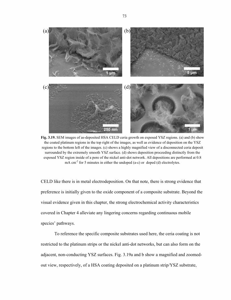
adjacent, non-conducting YSZ surfaces. Fig. 3.19a and b show a magnified and zoomed-
out view, respectively, of a HSA coating deposited on a platinum strip/YSZ substrate,
Fig. 3.19. SEM images of as-deposited HSA CELD ceria growth on exposed YSZ regions. (a) and (b) show the coated platinum regions in the top right of the images, as well as evidence of deposition on the YSZ
regions to the bottom left of the images. (c) shows a highly magnified view of a disconnected ceria deposit surrounded by the extremely smooth YSZ surface. (d) shows deposition proceeding distinctly from the
exposed YSZ region inside of a pore of the nickel anti-dot network. All depositions are performed at 0.8 mA cm-2 for 5 minutes in either the undoped (a-c) or doped (d) electrolytes.
(a) (b)
(c) (d)

74
where the platinum region is toward the top-right and the exposed YSZ is toward the
bottom left in both images. Deposition is clearly observed on areas that are adjacent to,
but not in direct contact with, the electronically conducting platinum, even as far away as
10 µm. It should be stressed that YSZ is completely electronically insulating at room
temperature, so no pathway for electrons exists in these regions. A highly magnified view
from the same sample shows an entirely disconnected island of ceria deposited on the
exposed YSZ surface (Fig. 3.19c), which definitively debunks the notion that growth
initiates on the metal surface and then proceeds outward to the YSZ regions. Fig. 3.19d
shows deposit growth distinctly proceeding from the pores of the nickel anti-dot
substrate, again, where the YSZ is exposed to the electrolyte solution.
Both the HSA and thin film morphologies can be deposited on the YSZ surface.
Fig. 3.20 shows cascading images of a YSZ surface exhibiting clear, ubiquitous thin film
deposition. The roughness seen up close in Fig. 3.20a, b, and c is not the original YSZ
surface, as the single-crystal substrates are received highly polished to sub-nanometer
roughness, as measured by AFM (not shown). It should be mentioned that the sample
imaged in Fig. 3.20 was deposited at 0.8 mA cm-2, which is typically associated with the
HSA microstructure, but the cerium concentration in the undoped electrolyte solution was
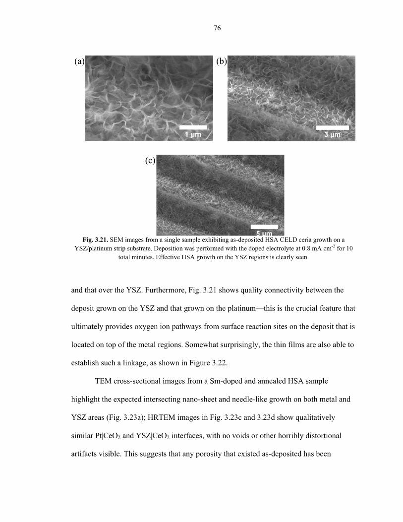
0.01 M, below the usual 0.05 M. This explains the planar growth. Fig. 3.21 shows the
HSA microstructure effectively grown on the YSZ spacing in between platinum strips,
with practically no distinction between the coating’s surface features over the platinum

75
Fig. 3.20. SEM images from a single sample exhibiting as-deposited planar CELD ceria growth on a YSZ/platinum strip substrate. Deposition was performed with the undoped electrolyte, but with a lower
(0.01 M) cerium nitrate concentration, and at 0.8 mA cm-2 for 5 minutes. Although this current density is typically associated with HSA structures, the lower cerium concentration leads to planar growth in this
case. The flat ceria deposit on the YSZ regions appears to extend microns away from the platinum strips.
(a) (b)
(c) (d)
(e) (f)
76
and that over the YSZ. Furthermore, Fig. 3.21 shows quality connectivity between the
deposit grown on the YSZ and that grown on the platinum—this is the crucial feature that
ultimately provides oxygen ion pathways from surface reaction sites on the deposit that is
located on top of the metal regions. Somewhat surprisingly, the thin films are also able to
establish such a linkage, as shown in Figure 3.22.
TEM cross-sectional images from a Sm-doped and annealed HSA sample
highlight the expected intersecting nano-sheet and needle-like growth on both metal and
YSZ areas (Fig. 3.23a); HRTEM images in Fig. 3.23c and 3.23d show qualitatively
similar Pt|CeO2 and YSZ|CeO2 interfaces, with no voids or other horribly distortional
artifacts visible. This suggests that any porosity that existed as-deposited has been
Fig. 3.21. SEM images from a single sample exhibiting as-deposited HSA CELD ceria growth on a YSZ/platinum strip substrate. Deposition was performed with the doped electrolyte at 0.8 mA cm-2 for 10
total minutes. Effective HSA growth on the YSZ regions is clearly seen.
(a) (b)
(c)

77
sufficiently removed by annealing at 650 °C for 2 hours in air, not surprising given the
small initial crystallite size [57]. Furthermore, the annealed grain size seen in Fig. 3.23b
and the selected-area electron diffraction pattern (see Appendix B) correspond well with
the XRD results above.
To have what is shown here in significant spatial deposition of ceria onto the metal-
adjacent YSZ surface, with a well-adhered and void-free interface is an all-but-certain
requirement for facile oxygen ion migration from the YSZ fuel cell electrolyte solution to
the ceria anode surface. Indeed, if the CELD of ceria only coated the metal, or if the
YSZ|CeO2 interface was poor, the conduction pathway for oxygen ions would be either
non-existent or highly resistive.
78
Fig. 3.22. As-deposited SEM images from the sample shown in Fig. 3.21, where connectivity between the thin film deposit grown on the YSZ regions and that grown on the platinum surface is seen.
YSZPt
CeO2
PtCeO2 CeO2YSZ
Fig. 3.23. TEM images showing definitive deposition on the exposed YSZ areas as a cross-sectional view (a); the polycrystalline nature of the deposit with annealed grain sizes ~15 – 20 nm (b); and HRTEM
Pt|CeO2 (c) and YSZ|CeO2 (d) interfaces. This sample’s deposition was performed at 0.8 mA cm-2 for 10 minutes with the doped electrolyte and annealed at 650 °C for 2 hours in air.
(a) (b)
(c)
(a) (b)
(c) (d)
79
3.4.4 HSA and Thin Film Transients
To understand how CELD deposits evolve over time, voltage and current transients of the
HSA and thin film morphologies are shown in Fig. 3.24 and 3.25, respectively. For a
given electrolyte solution composition and concentration, the steady-state current value
depends on the interplay between electrochemical reduction reactions, whose rates
collectively give the current density, and any blockages that cover the metal electrode
surface, which reduce the number of reduction reaction sites available. These blockages
include hydrogen bubbles that persist on the metal surface and any depositing nuclei, as
they, too, are electronically insulating.
Fig. 3.24 shows typical voltage transients for the HSA morphology at an applied
current density of 0.8 mA cm-2 on both platinum strip and nickel anti-dot metal network
configurations. All of the platinum strip substrates exhibit a double-plateau voltage
response. Using the chronological SEM images as guides (Fig. 3.24, I through IV), the
first plateau appears to be mostly related to deposition on the YSZ regions. A more
negative working potential is required to maintain the constant applied current density
once deposition begins to cover the platinum surface (Fig. 3.24, II, III, and IV).
Comparing the voltage response of Sm-doped 5-5µm (Fig. 3.24b) and Sm-doped 10-
10µm (Fig. 3.24c) patterns shows that the platinum pattern sizes do not affect the
transients much. There is, however, a significant difference between the undoped
electrolyte solution (Fig. 3.24a) and the Sm-doped electrolyte solution (Fig. 3.24b and
3.24c)—the undoped sample has a much shorter dwell time on the first plateau. This
suggests that the samarium doping partially inhibits the precipitation kinetics, requiring
80
0 50 100 150 200 250 300-0.9
-0.8
-0.7
-0.6
doped, Ni anti-dot
doped, Pt 10-10 µm
doped, Pt 5-5 µm
undoped, Pt 5-5 µm
(d)
(c)(b)
(a)
IVIIIIIIVo
ltage
/ V
Time / s
IIYSZ
Pt
PtI
YSZPt Pt
III
YSZ YSZPt
IV
YSZ
YSZ
Pt
Fig. 3.24. HSA voltage transients taken at 0.8 mA cm-2 for various electrolyte/substrate configurations: (a) undoped, platinum 5-5 µm; (b) doped, platinum 5-5 µm; (c) doped, platinum 10-10 µm; and (d) doped, nickel anti-dot. Also, chronological SEM images of doped, platinum 5-5 µm samples taken at the times
indicated by (I, II, III, and IV) on the transient plot.
81
longer times to deposit on the same YSZ area size. Also, the potential value for the
second plateau in the Sm-doped case is less negative than the undoped case, suggesting
that the Sm-doped deposit blocks the reduction reactions less, and is, therefore, more
porous. Ultimately, ubiquitous deposition occurs on the platinum and YSZ surfaces alike;
however, the SEM evidence in Fig. 3.19, 3.23, and 3.24 indicates that the deposit prefers
the YSZ to the metal surface initially. Judging from the relative amount of deposit seen to
coat the metal after ~5 minutes (Fig. 3.24, IV), it seems that once enough nuclei have
formed on the metal surface, continual deposition on those nuclei are preferred to the
distant YSZ surface nuclei.
The nickel anti-dot metal network substrate voltage transient has a qualitatively
different shape than its platinum strip counterpart. Consider that all HSA working
potentials, regardless of the substrate used, are relatively more negative, where both
oxygen reduction and hydrogen evolution are major contributors to the current density
[86]. However, less hydrogen evolution is observed for nickel-based substrates, meaning
that a more negative initial voltage is needed to induce enough ion motion in the liquid
electrolyte solution to satisfy the applied current density value. Eventually, the voltage
decreases and reaches a steady-state value less negative than that of the platinum strips,
probably because there are less hydrogen bubbles blocking reduction reaction sites.
The current transients for the thin film morphologies are shown in Fig. 3.25,
again, for platinum strips and nickel anti-dot networks. In this working potential region,
oxygen reduction is dominant [86], and can occur via a four-electron pathway (Eqn. 3.1)
or a two-electron pathway (Eqn. 3.2). The four-electron pathway has a higher steady-state
current than the two-electron pathway [82]. For both Sm-doped and Sm-doped + H2O2

82
electrolyte solutions, the steady state current for platinum substrates is higher than for
nickel substrates, possibly indicating a difference in the oxygen reduction pathway for the
two metals—platinum follows the four-electron pathway for acidic solutions and then at
pH 7 switches to 80% four-electron, 20% two-electron [96]. Comparably definitive
literature could not be found for nickel. Other possibilities are that the film is more dense
on nickel, or there still is a non-trivial hydrogen evolution-related current for platinum
but not nickel, even at these low cathodic potentials.
Higher steady-state current densities are seen in the Sm-doped + H2O2 electrolyte
solution than in the Sm-doped. This can be explained by recalling the Sm-doped + H2O2
0 10 20 30 400
500
1000
1500
2000
2500
3000
doped + H2O2, Ni
doped + H2O2, Pt
doped, Ni
doped, Pt
Cath
odic
Curre
nt D
ensit
y / µ
A cm
-2
Time / s
Fig. 3.25. Thin film current transients taken at -0.55 V vs. SCE for various substrate/electrolyte configurations. Here, Pt refers to platinum strip networks and Ni refers to nickel anti-dot networks.
83
CV scan in Fig. 3.18, where an appreciable current related to the reduction of Ce(IV)
intermediates is present. For the Sm-doped and Sm-doped + H2O2 electrolyte solutions,
typical thin film deposition rates are roughly 1.6 nm min-1 and 200 nm min-1,
respectively. These wildly disparate deposition characteristics should be distinguished
from and recognized as unrelated to their current transients; rather, the quickly forming
films with H2O2 addition indicate fast kinetics for the 𝐶𝑒(𝑂𝐻)2+2 route precipitation (Eqn.
3.9 – 3.11), as compared to the Ce(OH)3 route (Eqn. 3.8).
These time-dependent characteristics underscore the previously discussed notions
that unmistakable deposition occurs on the non-conducting YSZ regions, and that the as-
deposited coatings must be porous in order for a non-zero steady-state current to exist.