chapter 5 components, part 2—detectors and other circuits · eliminating the high-frequency...
TRANSCRIPT

C H A P T E R 5
Components, Part 2—Detectors andOther Circuits
In Chapter 4, we discussed dividers and oscillators. In this chapter we discussdetectors and other circuits that support PLLs. Detailed designs of phase detectors,lock detectors, and acquisition aids are studied.
Phase detectors are studied because understanding how phase detectors workis one of the major keys to understanding how PLLs work. Many systems use thelock detector to reset the system. This is a disastrous change to the operation ofmost systems. In a PLL, a reset can start the loop operating at a very low frequency(or with no output), which will then acquire lock at the normally much higheroutput operating frequency. Consequently, a small phase shift in the PLL thatwould marginally affect the system can cause a huge disruption in the operationof the system if a reset occurs. The key to lock detection is to alarm on behaviorthat shows that the PLL is broken. Quadrature phase detection, time-window edgecomparison, tune-voltage window comparator, and cycle-slip detection are thelock-detection methods that are covered.
Open-loop sweep, closed-loop sweep, and discriminator-aided acquisitions arethe methods that are covered. The phase/frequency detector uses discriminator-aided acquisition and is the most popular choice. Clock-recovery circuits cannotuse phase/frequency detectors. Consequently, these circuits require an acquisitionaid. Understanding the design details and trade-offs in these components is criticalin designing monolithic PLLs.
A charge pump and operational amplifier provide a method to convert thedifferential up and down outputs of the phase/frequency detector to a single-endedpositive and negative voltage source that charges and discharges capacitors in orderto control the VCO in a PLL. These components also are used in synthesizing theloop compensation. For this function, the component that most closely models anideal integrator is the best choice. Several different charge pump architectures arepresented, and trade-offs between each are discussed. Then, operational amplifiersare presented. The evolution of operational amplifier architectures to the one thatbest fits a PLL is shown. Finally, trade-offs between charge pump and operationalamplifier compensation designs are studied.
5.1 Phase Detectors
The phase detector in a PLL compares the reference-oscillator frequency with theVCO frequency and develops an error voltage for the loop to process. Consequently,
235

236 Components, Part 2—Detectors and Other Circuits
phase detector components have a critical impact on the performance of a PLL.Tracking range, acquisition range, loop gain, and transient response depend onthe characteristics of the phase detector. The major characteristics of a phasedetector include the input phase-difference range, the response to a frequencydifference, the sensitivity to input amplitude, and duty cycle.
This section begins by presenting the linear phase detector equations and afigure of merit for comparing phase detectors. Then, a variety of analog and digitaldevices for phase detection are presented, and the variety of different characteristicsare studied. Some have a simple topology, others operate at high frequency, andstill others have a very low content of undesirable signals in their output. Mixers,exclusive-OR gates, RS latches, flip-flops, and phase/frequency detectors are pre-sented. They represent the major types that are used to detect phase error inintegrated circuit PLLs.
5.1.1 Linear Model
Developing a linear model will help our discussion of phase detectors by giving usa standard for comparing the different types of phase detectors. Equation (5.1)establishes a linear model with an offset for a phase detector:
Vd = Kdue + Vdo (5.1)
where
Kd = phase detector gain (V/rad);
ue = phase error of the VCO output relative to the input signal;
Vdo = offset voltage, or ‘‘free-running voltage.’’
This linear model breaks down for large enough ue (phase error). The valuesof ue for which the linear model is valid define the range of the phase detector. Range,offset, and gain characteristics distinguish the differences between the detectors. Alarge offset with respect to the gain of the detector ruins the effectiveness of thedetector. Consequently, a figure-of-merit ratio will help compare the effectivenessof each detector circuit.
5.1.2 Phase Detector Figure of Merit
Is an offset Vdo = 193 mV too large for a phase detector to be effective? Theamount of output voltage per radian, which is the gain of the phase detector Kd ,determines the usefulness of the phase detector. Therefore, the ratio of outputvoltage gain to offset voltage, Kd /Vdo , indicates the size of the offset. We will callthis the figure of merit, M, of the phase detector as shown by (5.2):
M = Kd /Vdo (5.2)
For example, a phase detector with a gain of 5 V/rad and an offset of 193 mVproduces a figure of merit M = (5 V/rad)/(193 mV) = 26. A phase detector should

5.1 Phase Detectors 237
reasonably be expected to have M ≥ 15, and M as high as 500 is possible withcareful matching.
Range, offset, and gain characteristics distinguish the differences between thedetectors. However, they all share the same characteristics as a multiplier. A multi-plier has the characteristics of a phase detector by the trigonometric identity in(5.3):
sin(A) cos(B) = 0.5 sin(A − B) + 0.5 sin(A + B) (5.3)
We already studied this equation in Section 2.2, but we will review it here andadjust it for our linear model of a phase detector. Applying the trigonometricidentity for products of a trigonometric function to the multiplication of two signals(at frequencies RF and LO) produces (5.4):
V1(t)V2(t) = Vp1Vp2 0.5[cos(v rf t − v lo t + ue ) + cos(v rf t + v lo t + ue )](5.4)
Eliminating the high-frequency product with a lowpass filter yields (5.5):
V1(t)V2(t) = Vp1Vp2 0.5[cos(v rf t − v lo t + ue )] (5.5)
= Vpbeat cos(vbeat t + ue ) (5.6)
where
vbeat = v rf − v lo for v rf > v lo ;
Vpbeat = Vp1Vp2 × 0.5 × mixer losses;
Vpbeat = resulting voltage level after mixing (V).
The derivative of (5.6) calculates the incremental phase slope. For the mixeroperating with a 0 frequency difference (vbeat = 0, which is dc) and 90° phaseshift, the derivative of (5.6) produces (5.7) and (5.8):
Kd (f ) =d
df[Vpbeat cos(f )] (5.7)
Kd (ue ) = Vpbeat sin(ue ) (5.8)
Equation (5.8) shows the origin of the phase detector gain and that it relates tothe multiplication of two signals.
For ue equals p /2 rad (quadrature) in (5.8), Kd equals Vpbeat (V/rad). For ueequals 0 rad in (5.8), Kd equals 0 V/rad. This shows that maximum phase sensitivityoccurs for a 90° phase difference between the input signals, while a minimumphase sensitivity of 0 occurs for a phase difference of 0°. With the linear modelestablished, let’s look at the various phase detectors.

238 Components, Part 2—Detectors and Other Circuits
5.1.3 Balanced Mixer
First, we will look at a balanced mixer, sometimes called a double-balanced mixer,because it is very close to a four-quadrant analog multiplier. Furthermore, we willbegin by looking at diode ring mixers that are used in PCB design because theiroperation has been well established. Figure 5.1 shows a diode ring mixer. Thiscircuit consists entirely of passive components (baluns and diodes). Baluns anddiodes usually compose the major components in a ring mixer for PCB designs.These components allow operation at extremely high frequencies (>18 GHz) andacross wide frequency range.
5.1.3.1 Diodes
Only devices that have nonlinear current-voltage relationships or that change as afunction of time (are time-variant), or both, cause mixing products. Multiplicationof the two input signals yields one of the mixing products. A switch togglingbetween either a short or an open as a function of time makes a time-variant circuit.Mixers require very fast switching (at the LO frequency). In PCB designs, obtaininglow-noise figure and fast switching speed make Schotkey-barrier diodes the usualchoice in ring mixers. The nonlinear properties of diodes cause mixing products, sothe time-variant and nonlinear properties of diodes help produce mixing products.
Simultaneously applying two or more signals across a nonlinear diode causesmixing to occur. This action produces single- and multiple-tone intermodulationproducts. Two voltages applied in series across a diode cause the current throughit to contain the IF and higher-order intermodulation products of the two voltageinputs. A lowpass filter after the mixer must significantly reject these products tohave a good phase detector.
5.1.3.2 Baluns
Baluns are the other major components in a ring mixer. Inductive transformers ora microwave coupling structure are used for baluns. The balun balances the diodesand interfaces them with the unbalanced system. In addition, the balun current, I,
Figure 5.1 Diode ring mixer and transfer function of output voltage versus phase error.

5.1 Phase Detectors 239
matches system and diode impedance and provides interport isolation. The balunat the LO port provides the IF current return path to ground. Currents in the twobalanced leads of a balun are 180° apart in phase and ±90° out of phase withrespect to ground [1]. The amplitude and duty cycle of the input affect the phasedetector gain. Consequently, these circuits should be used with large input signals.
The mixer circuit in Figure 5.1 operates with any waveform; however, usinga square wave, like the Vo in Figure 5.2, eases understanding of the circuit’soperation. The switching voltage Vo ‘‘turns on’’ either the bottom two diodes(D3, D4) or the top two diodes (D1 , D2) depending on the polarity of Vo . Apositive Vo makes the bottom two diodes (D3 , D4) conduct. Vx equals the voltageat the midpoint of the secondary winding of transformer T2 , which is ground.Then, Vy = Vi , and Vdavg = 0.5Vy = 0.5 Vi . Similarly, a negative Vo makes the toptwo diodes (D1 , D2) conduct. Vy becomes effectively ground. Then, Vdavg = −0.5Vi .The bottom waveform in Figure 5.2 shows the resulting waveform of Vdavg .
To determine the transfer function for the mixer, several SPICE runs must bedone for several phase errors that cover the range of the detector (p ). Figure 5.3shows the average output voltage versus phase error for a mixer phase detector.Each curve is a SPICE run with a different phase-error difference input to themixer. A lowpass filter is adjusted to filter out the harmonics of the 5-MHz inputfrequencies and not cause long simulation times. In this case, the simulation wasadjusted so that the waveforms settle out in 2 ms with a 50-mV ripple. The remainingripple can be minimized by averaging the waveform over the time period from4 to 6 ms.
Figure 5.4 shows the transfer function plotted for mixer phase detector fromthe data shown in Figure 5.3. This figure shows the average detected voltage Vdavgversus sweeping phase error. As ue increases with time, the average componentVdavg varies sinusoidally. The maximum of the characteristic equals the phasedetector gain:
Figure 5.2 The switching waveforms in a diode ring mixer phase detector.

240 Components, Part 2—Detectors and Other Circuits
Figure 5.3 Average output voltage (lowpass filtered) versus phase error for a mixer phase detector.
Figure 5.4 Transfer function for a mixer phase detector (average voltage versus phase-error differ-ence in degrees).

5.1 Phase Detectors 241
Vdm = Kd = Vi /p (5.9)
This assumes that both transformers have primary turns equal to secondaryturns. A high signal amplitude Vi keeps Vdm high and gives the best figure of merit.For the operation as described above, the signal level of Vi should not cause adiode pair to conduct. This corresponds to Vi ≤ 1.2V for equal transformer ratio.The fastest slope is at −90° phase shift, and the slope is reduced for shiftsapproaching −180° or 0°. For the peak-to-peak voltage of 0.5V, we can calculatethe slope at −90°. From (5.8) this computes to 0.25 V/rad because V peak equalsV peak to peak divided by 2 (0.5/2).
A figure of merit M ≥ 400 can be achieved with well-matched diodes in anintegrated circuit that produce a Vdo of less than 1 mV. If low offset voltage of thephase detector is achieved, then the active loop filter usually becomes a significantcontributor. The active loop filter can have an offset voltage of 5 mV; however,high-performance opamps can be used that have an offset as low as 0.1 mV.
In Figure 5.5, two signals with different frequencies (5 MHz and 5.5 MHz)are connected into a mixer phase detector, followed by a lowpass filter. Thisconnection produces a sinusoidal output waveform that shows the sinusoidal shapeof the phase detector transfer function. This characteristic waveform will also beseen in other phase detectors and will explain some of the behavior that can occur.Figure 5.6 shows the CMOS transistor ring mixer that is equivalent to the diodering-based mixer. This connection can easily be integrated while the diode ringcannot.
Figure 5.5 Waveform that results from two input frequencies into the mixer, showing the shapeof the transfer function.

242 Components, Part 2—Detectors and Other Circuits
Figure 5.6 Schematic of CMOS ring mixer that can be used for a phase detector.
5.1.4 Gilbert Multiplier
The Gilbert multiplier circuit shown in Figure 5.7 also implements a four-quadrantmultiplier. This circuit does not have a balun and can be more easily integratedinto a monolithic circuit.
Figures 5.7 and 5.8 help describe the operation of the circuit. First, Vo splitsthe current I to the left as i1 or to the right as i2 , according to the characteristicshown in Figure 5.8. Vi splits the current i1 into currents i3 and i4 , according tothe characteristic shown in Figure 5.8. A similar characteristic holds for i2 . Similarly,Vi splits the current i2 into currents i5 and i6 . Combining the four currents produces(5.10):
Vdavg = (i4 + i6)R1 − (i3 + i5)R2 (5.10)
= (i4 + i6 − i3 − i5)R
where
R1 = R2 = R.
In practical applications, R1 and R2 have different values, which causes a dc offset;we will discuss this effect later in (5.14) through (5.17).
Now let’s study an equation for the average detected output voltage and itsassociated multiplier gain constant. Keeping Vi and Vo in the linear region of thecharacteristics in Figure 5.8 (amplitude less than 52 mV) produces (5.11) for theaverage detected output voltage Vd .

5.1 Phase Detectors 243
Figure 5.7 Schematic of CMOS Gilbert cell mixer.
Figure 5.8 (a) Transfer function for the bottom difference amplifier and (b) the left-hand-sidedifference amplifier in Figure 5.7.
Vdavg = KmViVo (5.11)
Km is a constant in volts−1 associated with the multiplier. Studying Figure 5.8gives us the calculation for the multiplier gain constant. If we assume all the tailcurrent I goes to i1 and none goes to i2 , i5 , and i6 , then from the transfer functionon the left-hand side of Figure 5.8 (i1 = VoI /52 mV). Again, if we assume that allthe current goes into i4 and none goes into i3 , then from the transfer function onthe right-hand side of Figure 5.8, i4 = Vii1 /52 mV. Substituting the previous

244 Components, Part 2—Detectors and Other Circuits
equation into the last gives i4 = ViVo I /(52 mV)2. Multiplying by R and comparingthe equation to (5.11) gives (5.12) for computing the multiplier gain constant:
Km = RI /(52 mV)2 (5.12)
Equation (5.13) computes the maximum voltage out of the phase detector, whichgives us the phase detector gain for sinusoidal inputs:
Kd = KmViVo (5.13)
From (5.8) Vdmax equals Kd . Now, with the detector gain computed, let’s look atthe offset voltages that occur in the Gilbert mixer.
The mismatch of the transistors and of the resistors is the source of offsetvoltages. A mismatch in the transistors causes input offsets Vio of a few millivoltsthat add to the inputs Vi and Vo . Similarly, a mismatch between R1 and R2 causesthe other offset to be added to the output. Equation (5.13) computes the effectsof the mismatch:
Voo = (R1 − R2)I /2 (5.14)
Next, let’s compute the average voltage at the output of the detector. Equation(5.15) computes the total expression for the output:
Vdavg = Km (Vi + Vio )(Vo + Vio ) + Voo (5.15)
= KmViVo + Km XVioVi + VioVo + V 2io C + Voo
Taking the time average, as we did in going from (5.3) to (5.6), gives (5.16):
Vd = Vdm sin(ue ) + Km (Vio )2 + Voo (5.16)
The dc terms in (5.16) can be combined as an effective offset voltage at the phasedetector output to give (5.17):
Vdo = Km (Vio )2 + Voo (5.17)
Figure 5.9 uses signal flow graphs to summarize these relationships for calculatingdc offset voltage.
Example 5.1
The Gilbert multiplier circuit in Figure 5.7 has a current I = 2 mA and resistanceR = 5 kV. R1 and R2 differ by 2%, and Vio = 5 mV. Find the dc offset Vdo , thegain of the phase detector Kd , and the figure of merit.
From (5.12) and (5.13), Km = (10V)/(52 mV)2 = 3,698, and Kd = ViVo(3,698).Kd depends not just on the circuit but on the input levels. The maximum Kd

5.1 Phase Detectors 245
Figure 5.9 Signal flow graph of calculations for dc offset in Gilbert mixer. (From: [2]. 1991Prentice-Hall. Reprinted with permission.)
corresponds to Vi = Vo = 52 mV, which is the largest signal that (5.8) holds. Then,Kd = (52 mV)2 3,698 = 10.0 V/rad.
From (5.14), Voo = (0.02R)I /2 = (100V) 2 mA/2 = 100 mV. Also, Km (Vio )2
= (5 mV)2 (3,698) = 93 mV. Then, by (5.16), the total offset is Vdo = 92 mV +100 mV = 193 mV. Then, from (5.2), the figure of merit for the multiplier isM = 10/0.193 = 51.8.
5.1.5 Exclusive-OR Phase Detector
An exclusive-OR logic circuit has essentially the same characteristics as an over-driven multiplier circuit. Overdriving the multiplier saturates the output at eithera positive value, corresponding to a logic ‘‘high,’’ or a negative value, correspondingto a logic ‘‘low.’’
A voltage at Vi in Figure 5.1 causes current to flow through either the left orright leg of the diode bridge, depending on the polarity of Vi . As the signal at Vichanges polarity, the conducting leg switches to the other side. This switchingaction inverts the polarity of a smaller signal at Vo as it appears at the output Vd .A negative or positive Vi and Vo input makes the output Vd positive. One positiveinput, with the other input being negative, makes the output Vd negative. The truthtable for a multiplier is shown in Table 5.1.
Comparing this logic with a truth table as shown in Table 5.2 shows themultiplier logically functions as an exclusive-NOR gate. Consequently, an over-driven multiplier is an exclusive-NOR, with ‘‘+’’ corresponding to a logic high (1)and ‘‘−’’ corresponding to a logic low (0).
Then, an exclusive-NOR gate can be used for phase detection. The transferfunction will have a triangular shape. In addition, an exclusive-OR gate can be
Table 5.1 Multiplier Truth Table
Vi Vo Vdavg
− − +− + −+ − −+ + +

246 Components, Part 2—Detectors and Other Circuits
Table 5.2 Exclusive-NOR GateTruth Table
Input Input OutputA B OUT
0 0 10 1 01 0 01 1 1
used. This gate just inverts the output logic. Consequently, a balanced output thatis both positive and negative, where Vdavg = Vbavg − Vaavg , uses an exclusive-ORoutput for Vaavg and its complement (exclusive-NOR) for Vbavg . Figure 5.10 showsa schematic of an exclusive-OR gate. This figure shows that it takes an inverterand four transistors to make an exclusive-OR gate. This is a minimum of transistorconnections a (total of six transistors).
Figure 5.11 shows two square-wave inputs (A and B) to the exclusive-OR gateand the resulting output waveform at OUT. To determine the transfer functionfor the exclusive-OR phase detector, several SPICE runs must be done for severalphase errors that cover the range of the detector (p ). Figure 5.12 shows thesemultiple SPICE runs for 5-MHz reference and VCO frequency inputs. The figurecontains lowpass-filtered output voltages versus phase error for an exclusive-ORphase detector. Each curve is a SPICE run with a different phase-error-differenceinput to the mixer. A lowpass filter is adjusted to filter out the harmonics andkeep simulation times down. For this case, the output waveforms are settled at2.5 ms. The remaining ripple can be minimized by averaging the waveform overthe time period from 2.5 to 4 ms.
Figure 5.13 shows a plot of the average value of the output as a function ofthe phase difference between inputs. The phase error is plotted as the ratio ofphase-error edge difference divided by the input source time period. This averagevalue, which results from lowpass-filtering the gate output, detects phase error
Figure 5.10 Schematic of an exclusive-OR gate.

5.1 Phase Detectors 247
Figure 5.11 Input and output waveforms of an exclusive-OR gate that is used as a phase detector.
Figure 5.12 Lowpass-filtered output of an exclusive-OR gate versus the variation of input phaseerror.

248 Components, Part 2—Detectors and Other Circuits
Figure 5.13 Transfer function of exclusive-OR phase detector showing average output voltageversus fractional phase error.
over a range of half a cycle before it starts repeating. For any input phase error,the ideal output does not contain any energy at the fundamental input frequency.At a 90° phase difference for the worst case, the second-harmonic has peak-to-peakamplitude 1.27 times the peak-to-peak range of the phase detector characteristic.
To generate the transfer function for a phase detector, we put in the samefrequency 5 MHz with varying phase. This transfer function controls the behaviorwhen the loop is close to lock. When the loop is unlocked, the phase detector hastwo different input frequencies. Figure 5.14 shows the PSPICE response of thedetector with two different input frequencies (5 and 4 MHz). Figure 5.15 showsthe unfiltered pulse-width modulation that comes out of the exclusive-OR gate.When this response is seen in other phase detectors, it shows the phase detectoracting like an exclusive-OR gate or a multiplier with saturated inputs. A PLL usesthe dc average of this waveform to acquire lock. As a rule of thumb, if thisfrequency difference is 10 times the loop bandwidth, lock will not be achieved, and
Figure 5.14 Exclusive-OR gate output for inputs with a frequency difference.

5.1 Phase Detectors 249
Figure 5.15 Lowpass-filtered (integrated) output of an exclusive-OR detector with a frequencydifference at the input.
a frequency-aided acquisition circuit will have to be used. Between 2 and 10 timesthe bandwidth, the loop will lock in an increasing amount of time, depending onthe frequency difference.
Lowpass-filtering the waveform in Figure 5.14 produces the waveform in Figure5.15. The x-axis is simulation time, and the y-axis is average voltage. The averagevoltage was computed in PSPICE by integrating the output voltage [V (2)] over theinput period (0.2 ms) and offsetting the waveform (2.5 × time) to make the resultingwaveform start at 0. The waveform in the figure shows the sawtooth transferfunction and looks similar to the filtered output of the mixer.
So far, we have assumed that the square waves at the input to the detectorhave a symmetrical shape. Consequently, the input waveforms have a 50% dutycycle. Suppose that A has a duty cycle of 20%, and B has a duty cycle of 40%,as in Figure 5.16. A duty cycle not equal to 50% produces a nonzero, free-runningvoltage and reduces Vdm of the phase detector characteristic. If either, or both, inputshas other than 50% duty cycle, the exclusive-OR phase detector characteristic willhave flat spots, as shown in Figure 5.16. The detailed harmonic content of theoutput of this type can be obtained as a function of duty cycle by Fourier analysis[2]. Using the digital exclusive-OR gate as a phase detector has the advantage ofgreater gain Kd , less offset Vio , and greater linear phase range.
5.1.6 RS Phase Detector (Two States)
An RS latch can be used as a phase detector and have similar characteristics to anexclusive-NOR gate. Figure 5.17 shows a schematic of the RS latch. Figure 5.18

250 Components, Part 2—Detectors and Other Circuits
Figure 5.16 Exclusive-OR average output transfer function with non-50% duty-cycle inputs.
Figure 5.17 Schematic of an RS latch.
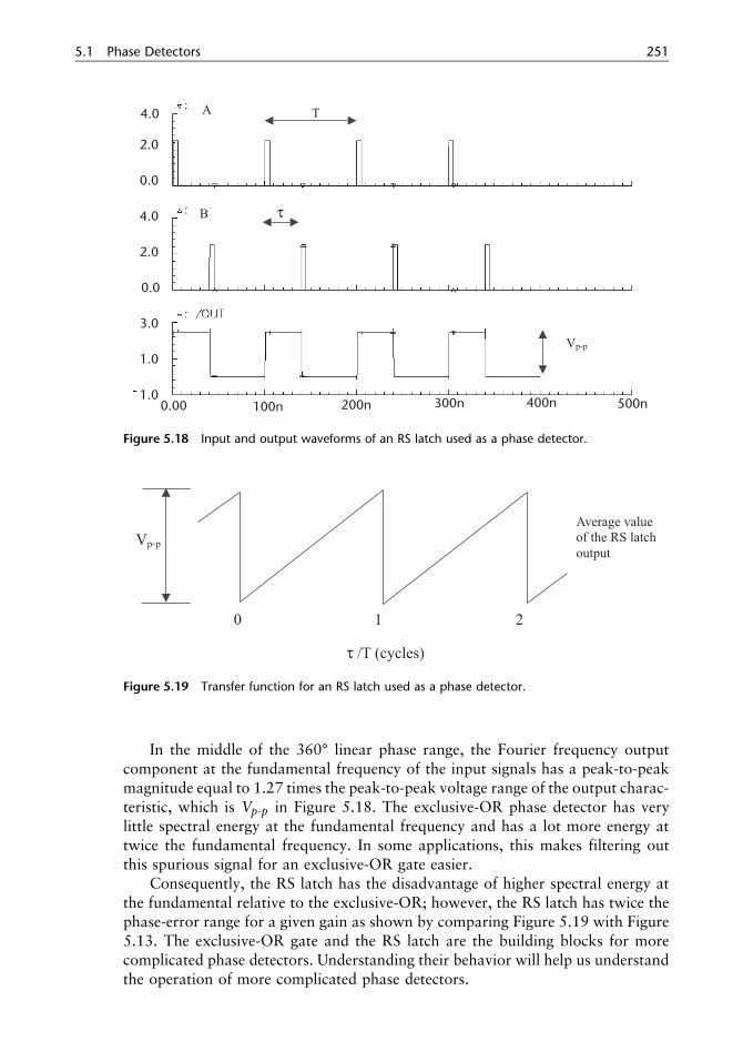
shows the expected waveforms for an RS latch used as a phase detector. The figureshows the input and output signals of the RS-latch phase detector. The input signalsA and B consist of narrow pulses. They connect to the set and reset inputs of aset-reset latch. The average value of the Q output is proportional to the phase atA relative to B. This creates a sawtooth transfer function of voltage versus phaseas shown in Figure 5.19. For either input with a finite width, the phase detectortransfer function has a flat spot that corresponds to the width at a corner. Forboth inputs with finite widths, the flat spot, or the sum of two flat spots, will beas wide as the wider input.
Connecting one signal of arbitrary width to the clock input of an edge-triggeredD flip-flop will give the same transfer function as the RS latch without causing theflat spot. Consequently, one edge of the waveform defines the switching time. Theother input connects to the set or reset input. This signal still must be narrow tominimize the flat spot.
5.1 Phase Detectors 251
Figure 5.18 Input and output waveforms of an RS latch used as a phase detector.
Figure 5.19 Transfer function for an RS latch used as a phase detector.
In the middle of the 360° linear phase range, the Fourier frequency outputcomponent at the fundamental frequency of the input signals has a peak-to-peakmagnitude equal to 1.27 times the peak-to-peak voltage range of the output charac-teristic, which is Vp-p in Figure 5.18. The exclusive-OR phase detector has verylittle spectral energy at the fundamental frequency and has a lot more energy attwice the fundamental frequency. In some applications, this makes filtering outthis spurious signal for an exclusive-OR gate easier.
Consequently, the RS latch has the disadvantage of higher spectral energy atthe fundamental relative to the exclusive-OR; however, the RS latch has twice thephase-error range for a given gain as shown by comparing Figure 5.19 with Figure5.13. The exclusive-OR gate and the RS latch are the building blocks for morecomplicated phase detectors. Understanding their behavior will help us understandthe operation of more complicated phase detectors.

252 Components, Part 2—Detectors and Other Circuits
Figure 5.20 shows input and output waveforms of an RS latch used as a phasedetector for unequal input frequencies (10 and 9.9 MHz). The bottom waveformshows the result of lowpass-filtering the output. This figure shows the pulse-widthmodulation in an RS flip flop (RSFF) that also occurs in an exclusive-OR gate fortwo input signals with different input frequencies (10 and 9.9 MHz). This waveformcharacteristic can be recognized in more complicated phase detectors.
5.1.7 Phase/Frequency Detector
This section studies the phase/frequency detector, which is one of the most com-monly used detectors. As you will see, understanding the phase/frequency detectoris key to understanding loop performance. First, we will study the gate logic. Next,we will cover the operating conditions. Finally, we will study the transfer functionof the phase detector.
Figure 5.21 shows the PSPICE model for the phase/frequency detector, whichis one of the most commonly used phase detectors [3, 4]. This model is based onlogic gates in the device. The schematic shows that four RS latches make up thephase/frequency detector. FF1 and FF2 control the up and down pulses, and FF3and FF4 control the reset signal for all the latches. The critical path is limited byjust three gate delays, two from the cross-coupled two-input NAND gates and onefrom the four-input reset NAND gate.
Figure 5.22 shows the relationships of up and down outputs to input waveformsby plotting the average voltage of the individual outputs u and d and the u-ddifferential combination output versus phase or frequency. The logic in Figure 5.22shows five possible phase detector relationships.
For the first relationship, the frequency of the VCO is greater than the frequencyof the reference. This condition causes the up output to have a low logic level with
Figure 5.20 Input and output waveforms for RS latch with unequal input frequencies.

5.1 Phase Detectors 253
Figure 5.21 PSPICE logic model for the phase/frequency detector.
small positive-going pulses and the down output to have approximately a 50%duty-cycle (pulse-width-modulated) waveform. In this condition, decreasing theVCO frequency will lock the PLL.
For the second relationship, the frequency of the VCO is less than the frequencyof the reference. This condition causes the down output to have a low logic levelwith small positive-going pulses and the up output to have approximately a 50%duty-cycle (pulse-width-modulated) waveform. In this condition, increasing theVCO frequency will lock the PLL.
For the third relationship, the frequency of the reference equals the frequencyof the VCO, and the phase of the reference lags the phase of the VCO. Thiscondition causes the up output to have a low logic level with small positive-going pulses and the down output to have positive-going pulses. In this condition,decreasing the VCO phase will lock the PLL.
For the fourth relationship, the frequency of the reference equals the frequencyof the VCO, and the phase of the reference leads the phase of the VCO. Thiscondition causes the down output to have a low logic level with small positive-going pulses and the up output to have positive-going pulses. In this condition,increasing the VCO phase will lock the PLL.

254 Components, Part 2—Detectors and Other Circuits
Figure 5.22 Relationships of up and down outputs to input waveforms.
In the third and fourth conditions, the phase difference between the referenceand VCO input determines the duty cycle of the positive-going pulses at the downand up outputs. Theory states that a 180° phase difference produces a 50% dutycycle.
In the fifth condition, the frequency of the reference equals the frequency ofthe VCO, and the phase of the reference equals the phase of the VCO. Thiscondition produces the lowest duty cycle and causes positive-going pulses out ofthe up and down outputs to occur simultaneously. This condition causes a phasedistortion in the transfer function [5].
Let’s use a SPICE model to see if we can generate the five relationships andto study the logic more closely. This can be accomplished by varying conditionsof the two input sources into the phase/frequency detector. Let’s use a referencefrequency of 2.5 MHz for the phase detector test. The higher-frequency speeds upthe simulation time and make it easier to see the narrow pulses on the plots. TheCD that accompanies this book shows the hierarchical SPICE deck for the phase/frequency detector. Now that the SPICE circuit is defined, let’s begin understandingthe operation of phase/frequency detectors by studying the frequency discriminatorfunction of the detector.

5.1 Phase Detectors 255
5.1.7.1 Frequency-Difference Response
Let’s look at the operation of the phase/frequency detector when the VCO frequencyis greater than the reference frequency. Figure 5.23 shows the response of thedetector for a reference frequency of 40 MHz and a VCO frequency of 50 MHz,as shown in the first two waveforms at the top of the figure. The up output hasnarrow pulses and the down output has a pulse-width-modulated output, as shownby the next two waveforms. The loop-compensation processes the pulse-width-modulated down output to push the VCO frequency lower toward the lock condi-tion. The next four waveforms in Figure 5.23 are the inputs to the four-inputNAND gate that generates a reset for the latches in the phase detector. The resetsignal is the last waveform in the figure. Next, the reset pulse, the up pulse, andthe positive edge of the reference are in synch. When the VCO positive edge lagsthe reference edge by half a period, the reset pulse resets the RS latch (v1) to getthe correct phase detector pulse width.
Figure 5.24 shows the response of the detector to a reference frequency of50 MHz and a VCO frequency of 40 MHz, as shown in the first two waveformsat the top of the figure. The reset pulse, the down pulse, and the positive edge ofthe VCO are in synch. When the VCO positive edge lags the reference edge byhalf a period, the reset pulse resets the RS latch (signal r1) to get the correct phasedetector pulse width. Next, the up output has pulse-width-modulated output, andthe down output has narrow pulses, as shown in the next two waveforms. Loop-compensation processes the pulse-width-modulated up output to push the VCOto a higher frequency.
Figure 5.23 VCO frequency greater than the reference frequency.

256 Components, Part 2—Detectors and Other Circuits
Figure 5.24 VCO frequency less than the reference frequency.
Pulse-width modulation in the up and down outputs of the phase/frequencydetector produces the frequency-discrimination mechanism; however, a potentialhang up in the transition from frequency detector to phase detector can be causedby the frequency-discriminator mechanism. At high modulation rates, the detectoris a frequency discriminator, and the high frequencies are filtered by the loop.However, at low modulation rates and at the edge of the transition from frequencyto phase detector, one of the outputs has a slowly varying pulse-width-modulatedbeat-note output, and the phase frequency detector acts like an exclusive-OR gate.Figure 5.25 shows the pulse-width-modulation output response of an exclusive-OR gate (equivalent to an analog multiplier) to a reference frequency of 2.5 MHzand a VCO frequency of 1.825 MHz. This output is like the down and up responsesof the phase/frequency detector in Figures 5.23 and 5.24.
The low-modulation-rate condition can occur for the phase/frequency detectorin a PLL with a high damping factor. A low-modulation condition can arise froma slow approach path to lock with only one side (up or down) of the phase detectoroperating. At the transition from frequency detector to phase detector, it has pulse-width modulation similar to the exclusive-OR gate. If this modulation is less thanthe modulation bandwidth of the VCO and greater than the loop bandwidth, theloop will have to pull the modulated waveform into lock. This pull into lock isthe same mechanism that analog PLLs use to achieve lock. This is a slow processthat significantly increases lock time. The phase detector uses the dc average ofthe modulated signal to pull into lock.
An example measurement of a PLL shows the pull-into-lock mechanism thatwe have discussed. The PLL has a 270-MHz output frequency, 100-kHz referencefrequency, 0.9 damping factor, and 5-kHz bandwidth. Figure 5.26 shows thezoomed-in transient response (output frequency on the y-axis and time on the

5.1 Phase Detectors 257
Figure 5.25 Output of exclusive-OR gate for different input frequencies.
Figure 5.26 Zoomed-in measurement of transient response of a PLL with 0.9 damping factor thatshows an analog pull-in mechanism.
x-axis) of the PLL, and it shows that the output frequency remains 50 to 120 kHzabove the locked frequency for 3.5 ms before it locks at 270 MHz. The settlingtime of 3.5 ms is much greater than the 1/5 kHz (200 ms) one would expect forthis loop.

258 Components, Part 2—Detectors and Other Circuits
Figure 5.27 shows the response of the example PLL with the damping factorchanged to 0.5 and a loop bandwidth of 6 kHz. The loop now settles to 270 MHzin 500 ms and has a more classic PLL transient. This is a sevenfold improvementover the previous response. Consequently, this figure shows that the PLL transientresponse can get hung up in the transition from the frequency-discriminator tophase detector mode on one side of the phase detector and rely on an analog pull-in method to attain lock. Consequently, for fast transient response, a 0.5 dampingfactor is optimum. This completes the discussion of the frequency-differenceresponse of the phase/frequency detector; we now move on to the phase-differenceresponses.
5.1.7.2 Phase-Difference Response
Let’s study the operation of the phase/frequency detector when the VCO andreference frequency are equal but the phases are different. Figure 5.28 shows thephase/frequency detector output when the VCO phase leads the reference-oscillatorphase, and their frequencies are equal to 50 MHz. The down output has a widepulse width, and the up output has narrow pulses. The down output results fromthe logic AND of signals V1 and /V2 . Also, the reset pulse, the up pulse, and thepositive edge of the reference are in synch. The reset pulse resets the RS latch (v1)to get the correct phase detector pulse width.
Figure 5.29 shows the phase/frequency detector output when the VCO phaselags the reference-oscillator phase. The down output has narrow pulses, and theup output has wide pulses. The up output results from the logic AND of signalsR1 and /R2 . Also, the reset pulse, the down pulse, and the positive edge of the
Figure 5.27 Zoomed-in measurement of transient response of example PLL that showed an analogpull-in mechanism with the damping factor changed to 0.5.

5.1 Phase Detectors 259
Figure 5.28 Phase/frequency detector output when VCO phase leads reference phase.
Figure 5.29 Phase/frequency detector output when VCO phase lags reference phase.
VCO are in synch. The reset pulse resets the RS latch (r1) to get the correct phasedetector pulse width.
Figure 5.30 shows that, for equal phase and frequency inputs, the up and downoutputs produce narrow pulses. This results from the four-input logic AND ofR1 , /R2 , V1 , and /V2 , which also generates the reset pulse. It is significant thatthe logic shows that output pulses should be present because measurements of

260 Components, Part 2—Detectors and Other Circuits
Figure 5.30 Equal phase condition for phase/frequency detector.
some phase detectors do not show these pulses. These zero-output measurementscan be explained by the effects of output loading, which eliminates these pulsesand causes a dead-zone problem.
5.1.7.3 Generation of Phase Detector Transfer Function
From the PSPICE simulations, the phase detector transfer function can be computedby varying the delay of one of the input signals and computing the average voltageof the resulting waveforms. First, let’s compute the output voltage versus the phaseof the phase detector by varying the delay (phase) of the VCO input in SPICE.
Figures 5.31 and 5.32 show phase/frequency detector outputs overlayed ontop of each other for the variation of the delay of the VCO with respect to thereference of −8 to 8 ns in 4-ns steps. Variation of delay is an equivalent phaseshift. Figure 5.31 shows the up output. The y-axis is voltage and the x-axis issimulation time. The falling edge of the up signal depends on the positive edge ofthe VCO input. The positive edge of the up signal stays fixed with the positiveedge of the reference input. For −8-ns, −4-ns, and 0-ns conditions, the up signalhas minimum pulse widths of 1 ns that are overlayed on top of each other andcentered at the simulation time of 26 ns. This figure shows that for a positive-

5.1 Phase Detectors 261
Figure 5.31 Up outputs versus delay in VCO phase.
Figure 5.32 Down outputs versus delay in VCO phase.
sloped VCO tune curve, increasing the tune voltage moves the falling up edge fromthe far right- to the left-hand side of the page and toward the positive referenceedge at the simulation time of 25 ns. The time period gets smaller so frequencyincreases.

262 Components, Part 2—Detectors and Other Circuits
Figure 5.32 shows the down output for the variation of the delay of the VCOwith respect to the reference of −8 to 8 ns in 4-ns steps. The y-axis is voltage andthe x-axis is simulation time. For negative phase errors, the positive edge of theVCO determines the rising edge, and the positive edge of the reference determinesthe falling edge. For positive phase errors of 0 ns, 4 ns, and 8 ns, the down signalhas a minimum pulse of 1 ns with the positive edge following the rising edge ofthe VCO and centered at simulation times of 26 ns, 30 ns, and 34 ns. This figureshows that, for a positive-sloped VCO tune curve, decreasing the tune voltagemoves the rising VCO edge from the far left- to the right-hand side of the pageand toward the positive reference edge at the simulation time of 25 ns. The timeperiod gets larger, so frequency decreases.
Figure 5.33 shows the average of the up output voltage waveform minus theaverage of the down output voltage waveform versus VCO delay. After 0.3 ms ofan RC-type time response, the averages have reached a steady-state dc voltage.The average value of the last 100 ns of this voltage is plotted against the delayvalue of the VCO to produce a phase transfer function. Figure 5.34 plots theprevious average dc voltage after 0.3 ms in Figure 5.33 and an additional ±18-nsdelay points versus the delay of the VCO. This figure shows a linear transferfunction going through zero phase error for the phase detector.
Calculations of the phase detector gain (Kd V/rad) are made from the slope ofthe phase detector transfer curve in Figure 5.34. The denominator of the gain is2 × p × 2 periods (one reference period = 20 ns) in the x-axis. The numerator is5V minus −5V in the y-axis. Dividing the numerator by the denominator computesa gain of 0.79 V/rad.
Finally, let’s summarize what has been found from the above analysis. First,there is always a pulse coming out of both outputs of the detector from a logic
Figure 5.33 Average of the up minus the down waveform versus VCO delay.

5.1 Phase Detectors 263
Figure 5.34 Phase transfer function for the phase/frequency detector.
viewpoint. This assumes no loading effects. There is no evidence of a dead zonebecause pulses are always present at the outputs, and Figure 5.34 shows a linearresponse around the 0° phase point where the dead zone should appear.
Phase Detector and Loop-Compensation InterfaceEarlier we mentioned that loading effects could cause the minimum pulses to beeliminated. Consequently, let’s look at loading effects on the phase/frequency detec-tor to see if they cause pulses to be eliminated and a dead zone in the phase detectortransfer function. The study of this interface consists of developing a PSPICE model,studying the stored charge on the loop-compensation capacitors, varying the delaybetween source inputs to vary phase relationship, varying capacitive loading, andcomputing the phase detector transfer function.
Let’s look at the model for the phase/frequency detector and loop-compensationinterface. To stay within the parameters of the evaluation version of PSPICE andto speed up calculations, an equivalent ECL output circuit is used and a 2.5-MHzreference frequency is used. The logic of the phase/frequency detector is replacedby voltage sources with a variable delay relationship. Figure 5.35 shows a PSPICEmodel schematic of the phase/frequency detector and loop-filter combination.
An active lowpass filter is used to model the effects of the loop compensationand also shows the circuitry used to measure the phase transfer function for thephase/frequency detector [6]. The included CD has a PSPICE netlist for studyingthe loading effects of the loop compensation on the outputs of the phase/frequencydetector.
With this circuit, the mechanism that stores the phase error in the loop compen-sation can be studied, and in Section 5.1.7.4 the dead zone in the phase transferfunction will be studied. First, Figure 5.36 shows charge being stored on eachcapacitor with the output waveform from the phase/frequency detector. Each pulse

264 Components, Part 2—Detectors and Other Circuits
Figure 5.35 PSPICE model of phase/frequency detector and loop-compensation interface.
Figure 5.36 Charge stored on feedback and input capacitors in a differential filter.
out of the phase/frequency detector is integrated and stored on the capacitors witheach phase comparison. Since the pulse width is a measure of the amount of error,the error is stored in the capacitors.
Figures 5.37 and 5.38 show four positive and three negative averaged-outputvoltage waveforms versus phase that are created for an ECL phase detector. The

5.1 Phase Detectors 265
Figure 5.37 For positive delays, averaged output voltage versus phase created from an ECL phasedetector.
Figure 5.38 For negative delays, averaged output voltage versus phase created from an ECL phasedetector.

266 Components, Part 2—Detectors and Other Circuits
average voltages of the last 2 ms are used to generate the phase detector transferfunction curve. The even voltage spacing shows that a linear transfer function curvewill be plotted. Consequently, we can use these plots to study the dead-zone effecton the phase detector transfer function curve.
5.1.7.4 Distortion Zone
The fifth condition of the phase/frequency detector, which has 0° phase differencebetween the inputs, causes a race condition in the IC. This race condition causesan undetermined state in the logic of the phase detector. In this condition, theoutput of the detector is sensitive to circuit-loading effects that can produce anonlinearity in the phase-versus-output-voltage transfer function of the phase detec-tor. This nonlinearity produces higher reference sidebands, loop instability, longerloop settling time, and higher phase noise.
The race condition depends on the rise and fall time and the propagation timeof the IC. Consequently, the width of the nonlinear distortion zone depends onthe rise and fall time and the propagation time of the IC. Rise and fall times andpropagation times decrease with higher-speed digital logic families. Consequently,a high-speed phase detector (MC12040 ECL) has a smaller dead zone than a lower-speed phase detector (MC4044 TTL) [6].
Let’s study the effects of loading on the phase detector transfer function byvarying the output capacitance. Figure 5.39 shows output voltage variation withcapacitive loading on the output level at a constant delay of 10 ns for a 400 ns
Figure 5.39 Variation of averaged phase detector output voltage for constant delay versus capaci-tive loading.

5.1 Phase Detectors 267
reference period. The reduction in output level with increasing load capacitanceshows an enhancement of the dead-zone problem.
Next, the phase detector transfer function curve is calculated with 10-nF capaci-tive loading. Figure 5.40 shows the resulting curve, which shows the dead-zoneeffect on the phase detector transfer function with the output capacitively loaded.
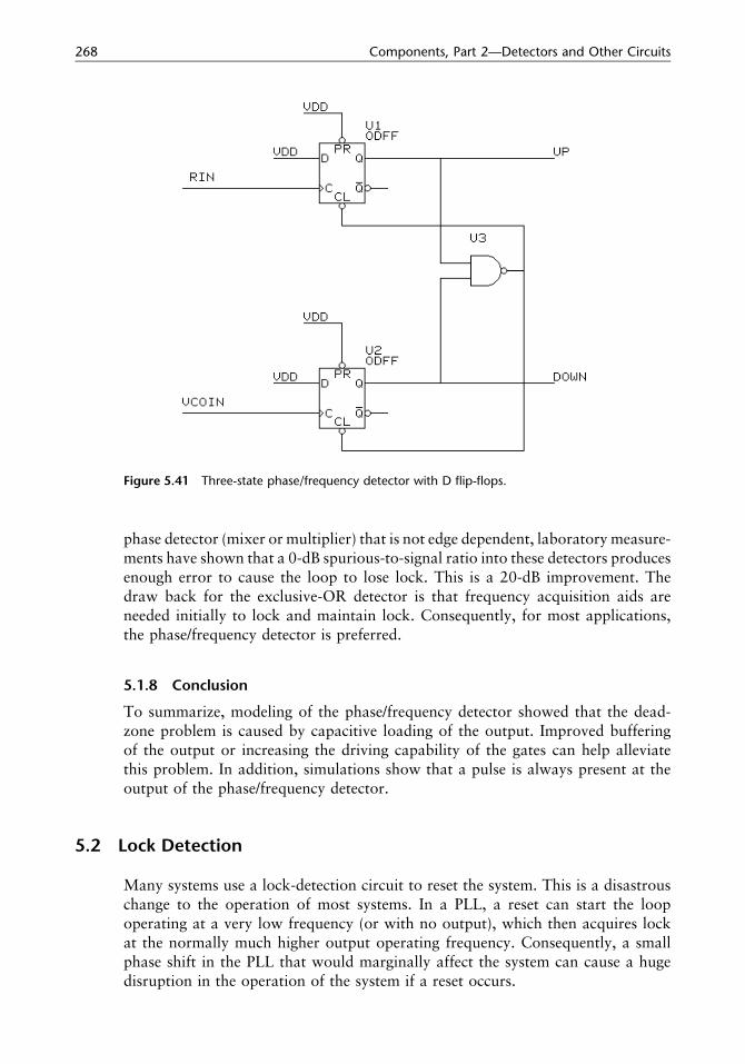
Finally, there are some application and design considerations in using phase/frequency detectors. First, Figure 5.41 shows another form of the three-state phase/frequency detector, which uses D flip-flops [2]. The input reference Rin connectsto the ‘‘clock’’ input of the top flip-flop. The VCO input connects to the ‘‘clock’’input of the bottom flip-flop. If Rin precedes VCOin , then the data input is logicone when the clock rises, the top flip-flop latches a one, and the output up isasserted. When the VCO edge occurs, the flip-flops are cleared. Similarly, if VCOinprecedes Rin , the flip-flop latches a one, and the output down is asserted. Whenthe Rin edge occurs, the flip-flops are again cleared. The flip-flops are usually amaster-slave dynamic topology. They have two transmission gates and two invertersto lower the device count and reduce silicon-area requirements. The conventionalCMOS circuit uses an input pass-transistor structure, which gives a longer setuptime than hold time, effectively introducing a time offset between Rin and VCOin .In addition, the setup and hold timing for the reset signal can cause a dead zoneor, in some cases, oscillation. Consequently, the RS flip-flop connection is preferredin most applications.
Next, the phase/frequency detector is an edge-sensitive device. Consequently,under noisy conditions (multiple clocks on rising edges of the input from thereference oscillator) can cause false pulse-width outputs that increase the error inthe loop and can eventually cause loss of lock. Laboratory measurements haveshown that at −20-dB spurious-to-signal ratio, the phase/frequency detector outputproduces enough false edges to cause the loop to lose lock. For an exclusive-OR
Figure 5.40 Dead-zone effect in phase detector transfer function from capacitive loading.
268 Components, Part 2—Detectors and Other Circuits
Figure 5.41 Three-state phase/frequency detector with D flip-flops.
phase detector (mixer or multiplier) that is not edge dependent, laboratory measure-ments have shown that a 0-dB spurious-to-signal ratio into these detectors producesenough error to cause the loop to lose lock. This is a 20-dB improvement. Thedraw back for the exclusive-OR detector is that frequency acquisition aids areneeded initially to lock and maintain lock. Consequently, for most applications,the phase/frequency detector is preferred.
5.1.8 Conclusion
To summarize, modeling of the phase/frequency detector showed that the dead-zone problem is caused by capacitive loading of the output. Improved bufferingof the output or increasing the driving capability of the gates can help alleviatethis problem. In addition, simulations show that a pulse is always present at theoutput of the phase/frequency detector.
5.2 Lock Detection
Many systems use a lock-detection circuit to reset the system. This is a disastrouschange to the operation of most systems. In a PLL, a reset can start the loopoperating at a very low frequency (or with no output), which then acquires lockat the normally much higher output operating frequency. Consequently, a smallphase shift in the PLL that would marginally affect the system can cause a hugedisruption in the operation of the system if a reset occurs.

5.2 Lock Detection 269
The key to lock detection is to alarm on behavior that shows the PLL is broken.A PLL can respond to a disturbance in a manner that makes it look like it isbroken. Consequently, the best lock-detection schemes will allow some time forthe loop to respond to a disturbance and recover. Otherwise, false alarms mayoccur. Quadrature phase detector, time-window edge comparison, tune-voltagewindow comparator, and cycle-slip detection are the most common methods forlock detection.
5.2.1 Quadrature Lock Detection
The quadrature phase detector technique as shown in Figure 5.42 uses two mixers(or analog multipliers) to compare the input reference with the in phase andquadrature phase of the fed-back VCO output. The in-phase comparison has a sinue output relationship with phase error, and the quadrature comparison has a cosue output relationship with phase error. The in-phase comparison is used to lockthe loop because sin ue ≈ 0, and the quadrature comparison is used to detect lockbecause cos ue ≈ 1. The quadrature detector output is followed by a lowpass filterand a threshold comparator. A dc level above the threshold indicates that thecircuit is locked. An unlocked loop produces a beat-note frequency at the outputof the quadrature comparator that is lowpass-filtered to 0-V input to the thresholdcomparator. Without the proper filter, the lock-detection signal will flicker on andoff because of noise, which will give false indications of lock or loss of lock.Too much filtering will cause an excessive delay in the lock or unlock signal.Consequently, the design of the output-smoothing filter is a vital part of a practicallock indicator. A compromise in the amount of smoothing is required. R. C.Tausworthe has performed a detailed analysis of the problem and has produceddesign curves [7, p. 88; 8, 9].
5.2.2 Tune-Voltage Window Comparator
A PLL can lose lock when the input frequency is to high, which pegs the tunevoltage close to the supply rail or when the input frequency is too low, which pegs
Figure 5.42 Block diagram of quadrature lock detection.

270 Components, Part 2—Detectors and Other Circuits
the tune voltage close to the ground supply rail. A tune-voltage window comparator,as shown in Figure 5.43, uses these two voltages to detect the unlocked condition.A tune-voltage window comparator monitors the tune line voltage with a highvoltage threshold and a low voltage threshold. Crossing either the high or thelow threshold causes an out-of-lock condition. Tune-voltage window comparisonrequires several operational amplifiers to achieve. Consequently, the size, powerconsumption, and threshold variation with process makes it impractical for inte-grated circuit design.
5.2.3 Time-Window Edge Comparison
The time-window edge comparison detector, as shown in Figure 5.44, uses anexclusive-OR gate to combine the up and down pulses out of the phase detector.Following the exclusive-OR gate with a lowpass filter rejects the narrow up anddown pulses and takes the dc average of the wider up and down pulses that occurwhen the loop is unlocked. Monitoring the dc voltage at the output of the lowpassfilter with a comparator sets a dc trip point when the loop is determined to be outof lock. Crossing the trip point to higher voltages sets the comparator to a highvalue (unlocked), and crossing the trip point to lower voltages sets the comparatorto a low value (locked).
This detection scheme has several disadvantages. First, the time-window edgecomparison (1 to 2 ns) will vary with process, which can cause false unlockconditions. The loop can have a constant phase offset that is out of the time windowand will indicate a false unlock condition. A larger capacitor value is needed toincrease the time window, which makes it consume area and renders it less integrat-able. An external disturbance can modulate the PLL so that the detector switchesbetween the locked and unlocked condition. Even worse, the loop control logicmay switch bandwidths when the loop is locked or unlocked. Switching bandwidthscan disturb the loop enough that the time-window edge-comparison detector tog-gles, which can cause an oscillation condition to occur.
Figure 5.43 Tune-voltage window comparator.

5.2 Lock Detection 271
Figure 5.44 Time-window edge comparison.
In summary, the time-window-edge-comparison technique is too sensitive andgives an excessive number of unlocked conditions. Special care must be taken forthis to be a successful implementation.
5.2.4 Cycle-Slip Detector
The cycle-slip detector detects frequency differences between its two input clocksthat remain different for a time period greater than the inverse of the frequencydifference. The detector generates a pulse when the phase/frequency detector outputpulse width rolls over from its largest pulse width to its narrowest pulse width.Figure 5.45 shows the schematic for the cycle-slip detector [10]. The cycle-slipdetector circuit consists of a phase/frequency detector, two cycle-slip detectors, anda final AND gate. The inputs to the circuit are the divided-down VCO waveformand the reference. The outputs of the phase/frequency detector are up pulses anddown pulses. The outputs of the cycle-slip detector are active, low, up cycle slipsand down cycle slips. A logical AND of the active, low, up cycle slips and downcycle slips produces an active, low cycle-slip detector output. This output is usedto reset a counter and count reference clocks between cycle slips. For example, if16 reference clocks are counted after a cycle slip, then the loop is set to the lockedstate by latching the carry out of the counter and disabling any further counts.Figure 5.46 gives an example connection for counting reference clocks after a cycleslip.
The cycle-slip detector does not detect loss of the reference clock or VCOfeedback clock. The cycle-slip detector requires that both input clock signals bepresent. With one clock missing, the output of the cycle-slip detector stays a constanthigh, which indicates a locked condition to the following circuitry.
Figure 5.47 shows the response of the lock detector with a ramped VCO frombelow the lock condition to above the lock condition. The x-axis value is 0.1 ns,which makes the minor divisions equal to 5 ns. The VCO ramps from 250 to400 MHz with the reference frequency set at 300 MHz. The left-hand side of

272 Components, Part 2—Detectors and Other Circuits
Figure 5.45 Schematic of cycle-slip detector.
Figure 5.46 Schematic for cycle-slip counter to create lock-detection output signal.
Figure 5.44 shows that the up output of the phase/frequency detector is a pulse-width-modulated signal for a VCO frequency greater than the reference frequency.The down output of the phase/frequency detector has constant narrow pulses,which indicates no response. On the far left-hand side, the 50-MHz difference ininput frequency causes a 50-MHz beat note in the pulse-width modulation outputof the phase/frequency detector. Using the rising edge of the VCO as a sampleclock to the reference waveform outlines a 50-MHz-period beat note. Using therising edge to rising edge of the VCO waveform as a cycle bin and reflecting thesebins on the pulse-width-modulated waveform output (VUP) of the phase/frequencyshows a cycle bin where no edges occur. This is a cycle-slip up pulse condition.Sampling this nonresponse latches the cycle slip and causes one pulse per beat note.
The right-hand side of Figure 5.47 shows that the down output of the phase/frequency detector is a pulse-width-modulated signal for a VCO frequency greater

5.2 Lock Detection 273
Figure 5.47 Response of the lock detector with a ramped VCO from below the lock condition toabove the lock condition.
than the reference frequency. The up output of the phase/frequency detector hasconstant narrow pulses, which indicates no response. A cycle bin of the downoutput where no edges occur causes a cycle-slip down pulse to occur. The beatnote on the high-frequency side does not represent the frequency difference becauseof aliasing in the sampling. In the middle of the figure, VCO and reference inputfrequencies are equal. The up and down cycles have no response. The bottomwaveform shows the response of a simple 4-bit counter to generate a lock-detectsignal. The wait time for the counter is set to 16. After 16 reference periods, thecarry out of the counter goes high, and the counter is disabled until the next cycleslip occurs.
5.2.5 Cycle-Slip Detector Versus Time-Window Comparator
Another example compares the performances of a time-window comparator anda cycle-slip detector. The PLL has a 10-MHz input frequency and multiplies theinput frequency by 24. The control system has a natural frequency of 300 kHzand a damping factor of 0.3.
Figure 5.48 shows a normal frequency and phase response of a PLL to a 1-MHzfrequency step in the reference frequency. A time-window comparator set to ±10°would give an out-of-lock indication because the 10° threshold would have beencrossed. In addition, the time-window comparator would toggle several timesbecause the ±10° threshold would have been crossed several times. The cycle-slipdetector would not alarm because 360° phase shift did not accumulate.

274 Components, Part 2—Detectors and Other Circuits
Figure 5.48 Frequency and phase-error response of a PLL to a 1-MHz frequency step in the referencefrequency.
Figure 5.49 shows a normal frequency and phase response of a PLL to a2.5-MHz frequency step in the reference frequency. Here, the cycle-slip detectoris on the verge of alarm. Consequently, this figure shows that the cycle-slip detectoralarms with frequency steps greater than 2.5 MHz. Figure 5.50 shows a normalfrequency and phase response of a PLL to a 50-ns phase step. Here, the time-window comparator would again have multiple alarms, but the cycle-slip-basedlock detector would not alarm.
Figure 5.49 Frequency and phase-error response of a PLL to a 2.5-MHz frequency step in thereference frequency.

5.3 Acquisition Aids 275
Figure 5.50 Frequency and phase-error response of a PLL to a 50-ns phase step.
Figure 5.51 shows the toggling of a window phase comparator versus solidcycle-slip lock detectors. A PLL with 16-MHz input reference frequency and128-MHz output frequency shows how the lock detectors operate. The x-axis hasthe units of nanoseconds. The top waveform shows the tune voltage to the VCO,which shows that the loop locks after 2 ms. The second waveform shows the time-window lock detector. It starts toggling at 1.7 ms and continues to toggle. Thebottom waveform shows the response of the cycle-slip detector with a state machinethat waits 32 reference clock periods after no cycle slips occur. The cycle-slipdetector detects lock at 5.3 ms and does not toggle after detection.
5.3 Acquisition Aids
If you cannot use a phase/frequency detector, then you will need an acquisitionaid. One circumstance occurs for clock-recovery applications. In clock recovery,
Figure 5.51 PLL transient response that compares a time-window and cycle-slip lock detectors.

276 Components, Part 2—Detectors and Other Circuits
multiple false locking conditions and missing clock edges occur. These conditionsconfuse the phase/frequency detector, and an exclusive-OR gate detector is generallyused. Another circumstance occurs in frequency-generation applications. After theother loops are locked, the VCO in the translation loop is tuned to the lockcondition. In only a narrow portion of the VCO tune range does the phase detectorhave an input. Otherwise, there is no input to the phase detector. Consequently,an acquisition aid must be used to tune the VCO until the phase detector gets aresponse.
In this section, we will study acquisition with an open-loop sweep and a closed-loop sweep and discriminator-aided acquisition. So, let’s look at these acquisitionstrategies in more detail.
5.3.1 Open-Loop Sweep
As shown in Figure 5.52, a sweep can be applied to a type 2 loop in the simplemanner of switching a current source in and out of the circuit. When the currentsource is connected, the voltage sweeps up, and when the current source is discon-nected and there is no lock, the voltage sweeps down from the discharging of thecapacitor. Otherwise, a separate sawtooth generator must be added to sweep thevoltage directly into the VCO [7, pp. 79–87; 11, pp. 227–234; 12].
The phase detector has a maximum output of Kd rad. The output from thephase detector produces a current of Kd rad/R1 into C in an active filter. Thiscurrent causes a voltage ramp of slope Kd rad/R1C. The voltage ramp on the VCOtune line produces a frequency change with a slope that is described by (5.18):
KdKv /(R1C) = v 2n (5.18)
The frequency ramp in (5.18) is related to the natural frequency vn from servomechanical definitions. Ramping the frequency faster will keep the loop unlocked.For a short time, the frequency can move faster due to the zero R2C in the filter.
Figure 5.52 Open-loop sweep circuit for lock-acquisition aid.

5.3 Acquisition Aids 277
A sudden change at the input to the active filter will be multiplied by R2 /R1 andimmediately appear at the filter output; however, the sustained ramp cannot movefaster than (5.18). A lowpass pole from placing R across C reduces the currentinto C and the slope. In addition, a loop that cannot hold lock on an input signalwill not be able to acquire lock on that input signal. Consequently, the maximumhold lock of v 2
n for a swept-input frequency applies to the acquisition limits. The100% probability of acquiring lock with a swept input depends on the sweep rateand the amount of noise.
The sweep frequency circuit must be shut off once lock has been achieved.Shutting off the sweep circuit prevents loss of lock and reduces reference sidebandsfrom loop-error corrections. In a closed loop, the tracking of the loop allows someleeway in time before turning off the sweeper; however, an open-loop sweep requiresa quick detection of frequency agreement and a rapid shut off of the sweep.
5.3.2 Closed-Loop Sweep
One method for closed-loop sweep requires a positive-feedback circuit. Addinglow-frequency positive feedback, as shown in Figure 5.53, causes the loop filterto oscillate, which sweeps the VCO frequency. When the loop locks, the largeamount of negative feedback dominates the local positive feedback, which sup-presses the oscillation and allows the loop to track normally. The feedback networkcan be a Wien bridge, and the limits of the sweep are set by the supply limits ofthe operational amplifier.
5.3.3 Discriminator Aided
Figure 5.54 shows a discriminator-aided frequency acquisition. This method hasa phase detector loop and a frequency detector loop. With the loop out of lock,the frequency loop controls the VCO, and the phase loop has little effect. Afterlocking, the phase loop has much greater dc gain than the frequency loop to
Figure 5.53 Closed-loop, low-frequency, positive-feedback sweep.

278 Components, Part 2—Detectors and Other Circuits
Figure 5.54 Discriminator-aided acquisition with separate phase and frequency detectors. (From:[7, pp. 79–87]. 1979 Wiley Interscience. Reprinted with permission.)
dominate control of the VCO. Consequently, at lock, the discriminator canbe disconnected. For a type 2 PLL, the transfer function for the frequency loopcan be a type 1, which means function block F2(s) can be a simple integrator[7, pp. 79–87].
Figure 5.55 shows another discriminator-aided acquisition method. For thismethod, the frequency loop and phase loop share the same integrator. The responseof the loop remains type 2, and the frequency path only adds to the dampingfactor. The frequency loop can remain connected if the relative contributionsbetween the frequency and phase loops are adjusted to maintain the desired dampingfactor [7, pp. 79–87]
In a closed loop with frequency sweep activated, the coherent operations in aPLL allow locking to an input signal with low SNR. A discriminator does notdistinguish between signal and noise. Consequently, for SNRs less than 6 dB, thesweep search may not successfully lock onto the input signal.
Figure 5.56 shows a frequency-difference detector (quadricorrelator). Equationsin the figure describe the signal paths. The quadricorrelator mixes the input signalwith an in-phase and quadrature output of the VCO to generate an in-phase andquadrature output of the frequency difference. Differentiating one signal pathand mixing the two together produces a product that contains a dc componentproportional to the frequency difference. Differentiating one signal path with a

5.3 Acquisition Aids 279
Figure 5.55 Discriminator-aided acquisition with frequency and phase loops sharing the same discriminator.(From: [7, pp. 79–87]. 1979 Wiley Interscience. Reprinted with permission.)
Figure 5.56 Quadricorrelator frequency-difference detector. (From: [7, pp. 79–87]. 1979 WileyInterscience. Reprinted with permission.)
highpass filter section disconnects the quadricorrelator for very small frequencydifferences, which allows the phase detector loop to take control of the VCO. Thelowpass filters in the in-phase and quadrature signal paths suppress the intermodula-tion products out of the mixer and limit the operating range of the circuit. Usingthe in-phase signal path for the phase detector in the PLL reduces the complexityof the circuitry [7, pp. 79–87].

280 Components, Part 2—Detectors and Other Circuits
5.4 Charge Pumps
The charge pump in a PLL converts the differential up and down outputs of thephase/frequency detector to a single-ended, switched, positive and negative currentsource that charges and discharges a capacitor in order to control the VCO in aPLL. The number of its parameters makes the charge pump one of the mostimportant circuits in a PLL (second to the VCO). The linearity of this circuit affectsthe stability of the loop, the amount of jitter, the amount of noise, the referencesideband levels, the phase tracking error, and the limits of the frequency operatingrange. The amount of peak charge pump current affects the amount of noise, theloop bandwidth, and the frequency slew rate of the PLL.
A charge pump consists of two switched-current sources driving a capacitiveload as shown in Figure 5.57. The left part of Figure 5.57 shows the functionalblock diagram, and the right part of Figure 5.57 shows a simple implementationin CMOS. An up pulse out of the phase frequency detector turns a p channelMOSFET on to charge the capacitor in the positive voltage direction. A downpulse out of the phase/frequency detector turns an n channel MOSFET on todischarge the capacitor in the negative direction. For a pulse of width T, currentI1 deposits a charge equal to I × T on the capacitor Cp . As the phase errorapproaches zero, zero charge accumulates on the capacitor, and the voltage ideallyremains constant [13].
Example 5.2
A phase/frequency detector drives a charge pump with a current source of 1 ma.Calculate the phase detector gain. If the charge pump has a figure of merit of 10,calculate the offset current for each current.
Figure 5.57 (Left) Functional diagram of phase/frequency detector with charge pump combination and(right) simple schematic of phase/frequency detector with a high-current charge pumpcombination.

5.4 Charge Pumps 281
The charge pump gain is the charge pump current divided by the range of thephase detector, which is 2p for the phase/frequency detector. Consequently, thecharge pump gain is 1 ma/2p = 0.159 ma/rad. Dividing the charge pump gain0.159 ma/rad by the phase detector figure of merit 10 computes the offset currentat zero phase error to be 0.159 ma/rad/10 = 0.0159 ma.
Figure 5.58 shows a test fixture for charge pumps that helps generate the chargepump transfer function. This figure shows an ideal operational amplifier after thecharge pump that processes the current out of the charge pump for testing purposes.The operational amplifier presents a high impedance load back to the charge pumpoutput at the voltage that is set by VCPO. The high input impedance of theoperational amplifier isolates the voltage source from the charge pump. Conse-quently, the output voltage to the charge pump can be varied from one supply railto the next without loading down the charge pump. When switches S1 or S2 areclosed, the current must go through the R1 feedback resistor because of the negativefeedback around the amplifier. Consequently, measuring the current in R1 in aSPICE simulation measures the current sourced by the charge pump. Finally, thecapacitor C1 is used to attenuate high-frequency switching spikes that can occur.Figure 5.59 shows a low-current version of the charge pump where transistors arecascoded to make a better current source.
Figure 5.60 shows a differential charge pump, which is another variation. Adifferential charge pump can help minimize the distortion in the transfer function.In this circuit, the control from the phase detector turns on only pull-down currents.The control signals switch differential pairs M1 − M2 and M3 − M4 . The pull-upcurrents Ip are always present. Consequently, if up and down controls are in thelow state, a common-mode feedback circuit consisting of transistors M5 − M9counteracts the pull-up currents to set a proper output common-mode level at
Figure 5.58 Circuit to process the output of a charge pump and generate the transfer function.

282 Components, Part 2—Detectors and Other Circuits
Figure 5.59 Schematic of low-current charge pump.
VGS5 + VGS9 . Each phase comparison momentarily disturbs the common-modelevel. Consequently, care must be taken to avoid common-mode transients thatcan lead to differential settling components.
A dead zone can occur for a charge pump. If the output pulse widths of thephase/frequency detector are small, and there is not enough drive current or thereis a high load capacitance, then the logic level will not be high enough to turn thecharge pump on. This causes a low-gain time width around the zero phase pointwhere a PLL locks. Zero phase detector gain makes the loop unlock and drift untilenough error is generated to cause a correction. Consequently, the amount of jitterthis causes is proportional to the time width of the dead-zone area.
Current offsets, transistor mismatches, and charge sharing can cause errors inthe transfer characteristics of the charge pump. This can cause an offset anddistortion in the transfer characteristics of the charge pump. An offset in the transfercharacteristics of the charge pump produces a constant pulse width out of thecharge pump when the loop is locked. This pulse width adds to the output jitterof the PLL.

5.4 Charge Pumps 283
Figure 5.60 Schematic of a differential charge pump.
Using a charge pump has several advantages. Charge pumps have a simpleimplementation that takes up less area. In addition, this circuit has potential forhigh-frequency response. Finally, a charge pump is the preferred implementationfor a loop filter outside an integrated circuit because it minimizes the number ofexternal components (only needs one large capacitor, a smaller roll-off capacitor,and one resistor.
Using a charge pump also has some disadvantages. Any imbalance of the twotransistors can cause a dead zone in the transfer function response. Charge sharingin the parasitic capacitors of the output transistors can be one of the major causesof this imbalance. Furthermore, to get narrow-bandwidth PLLs requires reducingthe charge pump gain. At some level this causes a low SNR with these low currents,which adds noise to the PLL over the reference phase noise. Eventually, with alow enough SNR, the loop will not lock.
Next, an ideal charge pump with infinite gain requires an infinite outputimpedance. A practical charge pump has a finite output impedance, which signifi-cantly reduces the gain from the ideal charge pump case. Consequently, the finiteoutput impedance of a practical charge pump gives a low gain when compared tooperational amplifiers. This low gain reduces the PLL’s tracking effectiveness andinsensitivity to disturbances.
Next, as discussed previously, the imbalance of the charge pump transistor cancause an offset in the transfer function, which reduces the figure of merit. The high

284 Components, Part 2—Detectors and Other Circuits
output impedance of a charge pump produces a significant slew-rate limit. If alarge frequency step occurs, the loop is slew-rate limited by the charge pumpcurrent. This would be a disadvantage for frequency-hopping applications.
As discussed earlier, charge sharing is one of the major causes of imbalance ina charge pump. The charge pump circuit in Figure 5.61 shows one method ofaddressing this problem [14]. Similar to the other charge pump circuits, the upand down signals from a phase frequency detector switch current sources Iup andIdn onto node Vcontrol . The selected current source delivers a charge to move Vcontrolup or down. Iup and Idn currents need to be equal to minimize offsets. Connectinga unity gain amplifier as shown in Figure 5.61 helps minimize these offsets. Theamplifier accomplishes this balance by biasing nodes N1 and N2 when they arenot switched to Vcontrol . This bias suppresses any charge sharing from the parasiticcapacitance on N1 or N2 .
Figure 5.62 adds the connection of the integrating capacitor in the loop filterand the parasitic capacitors of the output transistors to the charge pump connectiondescribed in Figure 5.61. Figure 5.62 shows the charge-sharing mechanism in thecharge pump attached to a loop filter. A pair of matched switched-current sourcescharges or discharges a dc current Io into or out of a filter capacitor (a large nchannel transistor), depending on the amount of phase error. The up and downswitch-control signals add charge or remove charge for a fixed time, which pumpsa fixed-size charge packet into or out of the capacitor on each cycle. The operationalamplifier connected as a unity-gain buffer provides a low-impedance version ofthe capacitor voltage, and its output VCTRL is sent to nodes N1 or N2 .
The unavoidable parasitic capacitance Cp at the current-source output charge-shares with the filter capacitor. This charge sharing produces a charge-error term.Clamping each parasitic capacitor Cp of the current source by using the unity gainamplifier that is not charging the filter capacitor to the Vcontrol voltage prevents
Figure 5.61 Differential charge pump with unity gain feedback to minimize charge sharing.

5.4 Charge Pumps 285
Figure 5.62 Loop-filter and parasitic capacitances that show charge-sharing effects in a differentialcharge pump with unity-gain feedback.
charge-sharing errors. Keeping the Vcontrol voltage on the parasitic capacitor Cpmakes a very small DV when the parasitic capacitor later connects to the filtercapacitor. Consequently, very little charge sharing can occur.
If one were going to use this approach, one might consider using the operationalamplifier itself to convert differential to single-ended input. However, if the applica-tion requires a 1-mF external capacitor from the IC, a charge pump would bebetter because only one external capacitor and pad would be necessary, whereasa differential operational amplifier configuration would require two external capac-itors and two pads. Many IC customers do not want this extra expense.
To show how the charge pump works, let’s use an example. For this example,we will use the simple high-current charge pump circuit shown in Figure 5.57. Itwill be connected to a test fixture by the method shown in Figure 5.58 in orderto get the transfer function.
Figure 5.63 shows the variation of charge pump transfer curve with outputvoltage. As the voltage approaches one rail or the other one of the output, transistorsstart to turn off, which causes an offset current. Furthermore, the gain of the chargepump detector varies with voltage and with negative and positive phase error. Atthe nominal condition (supply midpoint) of 2.5V, the negative phase-error slopeequals 295 ma/rad, and the positive phase-error slope equals 390 ma/rad. At 3.5Vthe negative phase-error slope decreases to 199 ma/rad, and the positive phaseerror slightly increases to a slope of 429 ma/rad. At 1.0V the negative phase-errorslope slightly increases to 356 ma/rad, and the positive phase-error slope decreases

286 Components, Part 2—Detectors and Other Circuits
Figure 5.63 Variation of simple charge pump transfer function with output voltage.
to 199 ma/rad. Different gains about the zero-error point can cause oscillations inthe loop, so that the loop never locks. A difference of less than 2-to-1 phase detectorgain between positive and negative phase-error should be maintained to avoidoscillations.
Figure 5.64 shows the variation of charge pump slope with nominal, weak,and strong process conditions. The transfer function was generated by varying thepositive-edge-to-positive-edge time difference between two 10-MHz input clockswith 50% duty cycles. For nominal conditions, the positive current phase-errorslope is 390 ma/rad and the negative current phase-error slope is 295 ma/rad. Forweak conditions, the positive current phase-error slope decreases to 219 ma/rad,and the negative current phase-error slope decreases to 127 ma/rad. For strongconditions, the positive current phase-error slope increases to 624 ma/rad, and thenegative current phase-error slope increases to 644 ma/rad. This is a 490% worst-case variation in-phase detector gain over process, which is a large variation.Furthermore, a 72% variation in positive to negative phase-error slope borders oncausing an unstable loop condition.
5.5 Design Considerations for Opamps in a PLL
An operational amplifier provides an alternative method to a charge pump. Theoperational amplifier in a PLL converts the differential up and down outputs ofthe phase/frequency detector to a single-ended positive and negative voltage sourcethat charges and discharges capacitors in order to control the VCO in a PLL. Thenumber of PLL parameters that the operational amplifier affects makes it one ofthe most important circuits in a PLL (second to the VCO).

5.5 Design Considerations for Opamps in a PLL 287
Figure 5.64 Variation of simple charge pump transfer function with process and temperature.
Listed in order of importance, the following operational parameters affect PLLperformance:
• Rail-to-rail output voltage swing ≥ (wide PLL frequency range);• High power-supply rejection ≥ (low jitter and low spurious);• Low differential offset bias current ≥ (low-jitter and low reference sidebands);• Wide input common-mode voltage range ≥ (wide PLL frequency range);• Wide bandwidth ≥ (low noise and jitter);• High dc gain ≥ (low tracking error and low noise);• Low-noise figure ≥ (low noise, low jitter, and improved PLL stability);• Output current loading ≥ (improved stability and low jitter);• Fast slew rate ≥ (fast PLL switching time).
The linearity of this circuit affects the stability of the loop, the amount of jitter,the amount of noise, the reference sideband levels, the phase tracking error, andthe limits of the frequency operating range.
Voltage offset of an operational amplifier is not a problem in PLLs because itoperates like a switch capacitor circuit with correlated double-sampling auto-zeroing. With the PLL close to lock, there are small changes in-phase error at therate of the reference-clock frequency. The amplifier offset is constant through thereference-clock period and its effect is held on the main integrator capacitor.The effect of the offset causes a onetime phase error (since it is constant) that issubtracted by the next phase-error sampling off the main integrator capacitor,which results in autozeroing of the offset of the amplifier.
We will begin the study of CMOS operational amplifiers for PLLs by studyingthe baseline two-stage amplifier and then comparing performance to this baseline.

288 Components, Part 2—Detectors and Other Circuits
Next, a folded-cascode operational amplifier is studied because of its high power-supply ripple rejection, which is crucial for PLLs. Then, the preferred AB-input,two-stage, folded-cascode operational amplifier is presented because it has highPSRR, low offset voltage, high output drive capability, rail-to-rail input operation,and rail-to-rail output operation. Rail-to-rail operation is the key to preventingthe loop from hanging up at either power rail.
5.5.1 Architecture Selection, Comparison to Basic Two-Stage Opamp
For PLL design, we must select the operational amplifier architecture that best fitsthe list of performances mentioned earlier in this section. We will select and studya basic, two-stage, differential amplifier followed by common-source amplifier-type architectures. The following describes the advantages and disadvantages ofsome of the differential amplifiers to be considered:
• Folded cascodes and telescopics:• Advantages:
• Good high-frequency power-supply rejection;• Disadvantages:
• Reduced output swing;• Higher offset voltage;• Reduced voltage gain.
• Class B:• Advantages:
• High output swing;• Good slew rate;• High gain.
The basic topology used for most CMOS opamps is shown in Figure 5.65. Adifferential input stage drives an active load, followed by a second gain common-source stage. An output stage may be added for driving heavy loads off-chip. Thiscircuit configuration provides good common-mode range, output swing, voltagegain, and common mode rejection ratio (CMRR) in a simple circuit that can becompensated with a single capacitor.
5.5.2 Basic Opamp
In this section we will analyze the various performance parameters of the CMOSoperational amplifier circuit. To do the analysis, we will define the transistorparameters for a 0.8-mm gate length with 5-V supply process and equations tohelp in the analysis and synthesis. Table 5.3 shows the transistor parameters. Wewill assume no loading of the first stage by the second stage because of the essentiallyinfinite input resistance of MOS devices. This allows us to separate the two stagesin order to find the voltage gain of the amplifier. Let’s look at the gain of the firststage.
Using the small-signal equivalent circuit for the transistors allows the voltagegain to be calculated. Equation (5.19) computes the first-stage voltage gain:

5.5 Design Considerations for Opamps in a PLL 289
Figure 5.65 Basic two-stage operational amplifier topology.
Table 5.3 List of 0.8-mm Gate-LengthTransistor Parameters Used in StudyingOpamps
Transistor Parameter Value
Uncox 191 mA/V2
Upcox 76 mA/V2
ln 0.33 mVlp 0.14 mV
Av1 =gmp2
gdsp1 + gdsn4(5.19)
where
gmp2 = transconductance of the input transistors;
gdsp1 = small-signal device-output conductance of the input transistor;
gdsn4 = small-signal device-output conductance of the active load transistor.
Similarly, (5.20) computes the second-stage common-source voltage gain:

290 Components, Part 2—Detectors and Other Circuits
Av2 =gmn6
gdsp5 + gdsn6(5.20)
where
gmn6 = transconductance of the second-stage common source transistor;
gdsn6 = small-signal device-output conductance of the second-stage commonsource amplifier;
gdsp5 = small-signal device-output conductance of the active load for thesecond-stage common-source amplifier.
Consequently, combining gain equations gives (5.21) to compute the overallgain:
Av =gmp2
gdsp1 + gdsn4
gmn6gdsp5 + gdsn6
(5.21)
The overall gain is thus related to the quantity (gm /gds )2 as shown by (5.22) and
(5.23).
gmgds
=2L
(Vgs − Vt )1
dXddVds
(5.22)
where
Vgs − Vt = effective gate source voltage;
Vds = drain to source voltage.
gmgds
=2L
(Vgs − Vt )1l
(5.23)
where
l = the output impedance constant (V −1).
Thus, the overall voltage gain is a strong function of the bias point chosen for thedevices and the channel length of the transistors used, and (Vgs − Vt ) = 0.2V forall devices.
Example 5.3
For example, consider a typical 0.8-mm gate length that has a channel-lengthmodulation parameter of 0.33 m /V for an n channel transistor and 0.14 m /V fora p channel transistor, and set (Vgs − Vt ) = 0.2V. Let’s apply these values to theopamp circuit in Figure 5.65 and calculate the gain for an n channel and p channeltransistor and the gain for the whole amplifier. For a typical 0.8-mm process,
5.5 Design Considerations for Opamps in a PLL 291
l has a value of 0.33 m /V for an N-channel MOS transistor and 0.14 m /V for aP-channel MOS transistor with 0.8-mm channel lengths.
Then (5.23) gives gm /gds of 25 = 2 × 0.8/(0.2 × 0.14) for NMOS devices and57 for PMOS devices. Equation (5.21) gives A = −25 × 57 = −1,385.
Example 5.3 shows that either increasing the channel length of the devicesused or reducing the bias current to reduce (Vgs − Vt ) increases the voltage gain.Unfortunately, both of these changes degrade the frequency response of theamplifier. Equation (5.24) computes the frequency bandwidth of the operationalamplifier:
v t =gmp2Cc
(5.24)
where
gmp2 = 2Idp2 /Vdsat (5.25)
where
Vdsat = (Vgs − Vt ).
For an Id2 current of 55 ma, a Vdsat of 0.2, and a miller compensation capaci-tance Cc of 1 pF, substituting the gmp2 (550 mmhos) results from (5.25) into(5.24) computes an 87.5-MHz bandwidth. Next, from high-frequency analysis, thestability of the operational amplifier can be computed as shown by (5.26):
upm =p2
− atan1gmp2Cc
gmp5CL2 − atan1
gmp2Cc
gmp5Cgsp5
2 (5.26)
where
CL = the output load capacitance.
Substituting the previous values and a load capacitance of 1 pF, a gmp5 of 1.7ma/V, and a Cgsp5 of 141 fF into (5.26) computes a phase margin of 69°.
Next, the systematic offset voltage can be computed as shown by (5.27)
Voscm =Vicm
CMRR=
Vicm
2gmp21
gdsp7gmn3
1gdsp2
(5.27)
where
Vicm = input common mode voltage.

292 Components, Part 2—Detectors and Other Circuits
Substituting an input common mode of 2.5V, gmn3 of 1.2 ma/V, gdsp2 of19 mmhos, and a gdsp7 of 26 mmhos into (5.27) computes an offset of 0.93 mV.Furthermore, (5.27) shows that the CMRR is related to the offset voltage; it isgiven by (5.28):
CMRR = 2gmp21
gdsp7gmn3
1gdsp2
(5.28)
Substituting the previous values into (5.28) computes a CMRR of 2,672. Furtherdegradation in offset can be expected due to the mismatch of the transistors in theprocess.
With the bandwidth computed, we now compute the slew rate of the amplifier,which depends on the miller capacitance and the loading capacitance of the opera-tional amplifier. Equation (5.29) computes the slew rate for the operational ampli-fier assuming no capacitive loading:
SR = Ip5 /Cc (5.29)
For an Ip5 bias current of 110 ma and a Cc miller capacitance of 1 pF, (5.29)computes a 110 V/ms slew rate.
Finally, let’s look at the PSRR of the operational amplifier. The PSRR to thepower supply is a function of the input transistor transconductance, mismatch withthe other input transistor transconductance, and the tail-current transistor outputconductance. Equation (5.30) shows this relationship:
PSRR =gmp2gdsp7
2gmp2Dgmp2
(5.30)
where
Dgmp2 = mismatch ratio between input transistors.
Using a Dgmp2 of 0.01% and the previous values for the other variables computesa PSRR of 47 dB (ratio of 232).
Thus, we find fundamental trade-offs between frequency response, gain, andoffset voltage in CMOS operational amplifier design. The above basic, two-stageamplifier with many variations has been widely used in a variety of applications;however, the evolution of several alternative circuits optimizes certain aspects ofthe performance of the amplifier. In the next section, we consider variations onthe basic circuit and alternative architectures.
5.5.3 Folded Cascode
Many modern IC applications need CMOS opamps designed to drive only capaci-tive loads. Capacitive-only loads make it necessary to use a voltage buffer to obtaina low output impedance for the opamp. Opamp designs that realize this buffer

5.5 Design Considerations for Opamps in a PLL 293
have higher speeds and larger signal swings than those that must also drive resistiveloads. Having only a single high-impedance node at the output of an opamp thatdrives only capacitive loads yields these improvements. All the other nodes in theseopamps have relatively low impedance from the admittance seen at all the othernodes, being on the order of a transistor’s transconductance. Having relatively lowimpedance on all the internal nodes maximizes the speed of the opamp. These lownode impedances also result in reduced voltage signals at all nodes other than theoutput node; however, various transistors can have quite large current signals.With these opamps, the load capacitance compensates the amplifier. Increasing theload capacitance usually makes the opamp more stable, but it also makes it slower.The transconductance parameter (i.e., the ratio of the output current to the inputvoltage) distinguishes these opamps from the other modern opamps. Consequently,they are sometimes referred to as operational transconductance amplifiers or trans-conductance opamps.
Figure 5.66 shows an example of such an amplifier. This circuit is also knownas the folded cascode. From CMOS amplifier theory, cascode configurationsincrease the voltage gain of CMOS transistor amplifier stages. A single common-source, common-gate stage gain can provide enough voltage gain for many applica-tions. This opamp configuration also has a high output impedance.
The design converts a differential input to single-ended output. All the currentmirrors in the circuit use wide-swing cascode current mirrors. The use of thesemirrors results in high-output impedance for the mirrors (compared to simplecurrent mirrors). This higher impedance maximizes the dc gain of the opamp. Eventhough a folded-cascode amplifier only has a single gain stage, it can have reasonablegain on the order of 700 to 3,000.
A normal cascode would have NMOS input devices MP1 and MP2 driving MN3and MN4 . For ac signals in Figure 5.66, the NMOS devices MN3 and MN4 foldthe cascode up to the PMOS input transistors MP1 and MP2 . This circuit is a
Figure 5.66 Schematic of a folded-cascode operational amplifier.

294 Components, Part 2—Detectors and Other Circuits
‘‘folded-up’’ version of a standard cascode. Additionally, this circuit simultaneouslyperforms a level-shifting function [15].
The folded-cascode opamp applies cascode transistors to the input differentialpair, but by using transistors opposite in type from those used in the input stage.For example, the input differential pair has p channel transistors MP1 and MP2 inFigure 5.66, and the cascode transistors have n channel transistors MN3 and MN4 .This arrangement of opposite-type transistors allows the output of this single gain-stage amplifier to be taken at the same bias-voltage levels as the input signals [16].
Now, for the other transistors, the current mirror composed of MP4 , MP7 ,MP8 , and MP9 converts differential output to single ended. The circuit in the figureuses a simplified bias network MP3 , MP8 , MN5 , and MN6 to simplify matters. Theintent here is to show the basic architecture. In practical circuits, the bias for IDP0might be replaced by a constant transconductance bias network.
The load capacitor CL determines the compensation by setting the dominantpole. In applications where the load capacitance is very small, it is necessary toadd additional compensation capacitance in parallel with the load to guaranteestability. If lead compensation is desired, a resistor can be placed in series withload capacitor CL . In some applications, lead compensation may not be possiblebecause the compensation capacitance is mostly supplied by the load capacitance;however, it is more often possible than many designers realize. For example, it isoften possible to include a resistor in series with the load capacitance.
The input differential-pair transistors have bias currents equal to IDP0 /2. Mak-ing the currents in current sources MN1 and MN0 larger than IDP0 /2 provides theproper bias to the transistors. The bias current IDN3 of one of the n channel cascodetransistors MN3 or MN4 , hence the transistors in the output-summing currentmirror as well, equals the drain current of MN0 or MN1 minus IDP0 /2. Consequently,this bias relationship gives (5.31) and (5.32):
IDN3 = IDN4 = IDN0 − IDP0 /2 (5.31)
IDN0 = IDN1 (5.32)
An Idp0 of 110 ma and IDN0 of 135 ma give an 80-ma current through IDN3and IDN4 . The ratio of (W /L)N1 or (W /L)N0 to bias transistor mirror MN5 estab-lishes the drain current IDN0 . Since the bias current of one of the cascode transistorsis derived by a current addition, for it to be accurately established, it is necessarythat both IDN1 and IDP0 be derived from a single-bias network. In addition, anycurrent mirrors used in deriving these currents should be composed of transistorsrealized as parallel combinations of unit-size transistors. This approach eliminatesinaccuracies due to second-order effects caused by transistors having nonequalwidths [16].
Let’s look at the two paths of the gain from input to output. A differential acinput voltage Vin causes gmp2 Vin /2 ac current to flow in the input transistors.This current flows from transistor MP2 through transistor MN4 to the output.Transistor MP2 has a common-source amplifier connection, and transistor MN4has a common-gate amplifier connection. From this connection, this circuit isalso known as a common-source, common-gate amplifier. The current through

5.5 Design Considerations for Opamps in a PLL 295
transistor MP1 flows through transistor MN3 and is mirrored by transistors MP8and MP7 through transistor MP4 and MP9 to the output.
Equation (5.33) computes the small-signal voltage gain of this circuit at lowfrequencies, which is a function of the input transistor transconductance and theoutput conductance contributions from MP9 and MN4 :
Av =gmp2
goutp9 + goutn4(5.33)
Equation (5.34) computes the output conductance contribution from MP9 :
goutp9 =gdsp9
1 +gmp9gdsp4
(5.34)
Equation (5.35) computes the output conductance contribution from MN4 :
goutn4 =gdsn9
1 +gmn4
gdsn0 + gdsp2
(5.35)
Substituting (5.33) into (5.35), an gmp2 of 1.03 ma/V, a gdsp2 of 18.6 mmhos, agmp9 of 0.93 ma/V, a gdsp9 of 13.9 mmhos, a gmn4 of 1.3 ma/V, a gdsn4 of 30.7mmhos, a gdsp4 of 14.3 mmhos, and a gdsn0 of 32 mmhos into the equation computesa gain of 57 dB (ratio of 756).
Next, let’s look at the stability of the amplifier. The load capacitance CLperforms the function of a compensation capacitor. This gives an important advan-tage to this circuit versus the previous circuit, which required the additional millercapacitance Cc to keep the amplifier from oscillating in a feedback loop connection.An important disadvantage of single-stage amplifiers is that the output voltageswing is degraded by the presence of the cascode transistors MN3 , MN4 , MP8 , andMP9 . A high-swing cascode configuration can be directly applied to the single-stage amplifier to improve the swing. The high swing cascode results in an availableoutput voltage swing that extends to within 2(VGS − Vt ) = 2 DVGST of each supply.
Analysis of the opamp begins with an expression for the gain. Equation (5.36)computes the gain bandwidth [17]:
v t =gmp2
CL + (Cdbn4 + Cdbp9)(5.36)
A capacitive load of 0.5 pF, MN4 drain capacitance of 26 fF, and MP9 draincapacitance of 55 fF substituted into (5.36) gives a 282-MHz unity-gain crossoverfrequency.
Next, stability is determined by evaluating the nondominant poles. We willuse the three-pole approximation for the frequency response as shown by (5.37):
upm = 90 − atanSv tp1D − atanSv t
p2D − atanSv t
p3D (5.37)

296 Components, Part 2—Detectors and Other Circuits
Pole 1 occurs at the junction of MN4 and MN0 . Equation (5.38) computes its value:
p1 =gmn4 + gmbn4Cdbn4 + Cdbn0
(5.38)
Pole 2 occurs at the junction of MP4 and MP7 . Equation (5.39) computes its value:
p2 =gmp4
Cgsp7 + Cdbp8(5.39)
Pole 3 occurs at the junction of MP9 and MP4 . Equation (5.40) computes its value:
p3 =gmp9
Cdbp9 + Cdbp4(5.40)
Other poles are less significant. A gmbn4 of 195 ma/V, a Cdbn0 of 33 fF, a gmp4of 1.01 ma/V, a Cgsp7 of 53 fF, a Cdbp8 of 68 fF, and a Cdbp4 of 79 fF substitutedinto (5.37) computes a phase margin of 59°. For design purposes, we check thatpoles 2 and 3 are more than 10 times greater than vt so that they do not affectthe stability of the amplifier and its crossover frequency point. Then, we adjustpole 1 to give us our phase margin.
Next, we analyze the slew rate. Equation (5.41) computes the slew rate of afolded cascode:
SR =Idp0
CL + (Cdbn4 + Cdbp9)(5.41)
Using an Idp0 of 110 ma, a CL of 0.5 pF, and the previous capacitor values computesa slew rate of 183 V/ms.
Figure 5.67 shows an AB-input, two-stage, folded-cascode operational amplifierfor rail-to-rail operation. The folded-cascode state is followed with a common-source push-pull output stage for current boosting, higher gain, and output rail-to-rail swing. This circuit has gain from any common-mode input to the operationalamplifier. This occurs because either the n channel or the p channel differentialamplifier will be turned on at one of the rails. This is important in PLL designs toprevent the loop from hanging up on either rail. As long as there is gain at therails, the integrator will operate and move the control voltage to the VCO backtoward the locking condition. The equations developed in the earlier designs canalso be applied to this design.
Table 5.4 compares the performance of operational amplifiers. This comparisonshows the strengths and weaknesses of each design architecture. OP27 and 741operational amplifiers are individual product ICs and are shown for reference. TheAB-input, two-stage, CMOS operational amplifier is preferred for PLLs.

5.6 Differences Between Charge Pump and Operational Amplifier Compensation 297
Figure 5.67 AB-input, two-stage, folded-cascode operational amplifier for rail-to-rail operation.
5.6 Differences Between Charge Pump and Operational AmplifierCompensation
One of the most important concepts to understand in PLL design is that synthesisof the compensation circuit only approximates an ideal integrator, which is neededto make an ideal type 2 PLL. A charge pump would have to have infinite outputimpedance, and an operational amplifier would have to have infinite gain in orderfor a compensation circuit to have an ideal integrator. Consequently, a decisionhas to be made as to which circuit makes a better integrator and what the differencein performance is.
Differences in performance show up in the following areas:
• Tracking a swept frequency;• Noise suppression in phase-noise plots;• Steady-state phase-error tracking.
5.6.1 Error Tracking of Charge Pump and Active Compensation
Active internal compensation allows better error tracking than charge pump com-pensation. An example design comparison between charge pump internal compen-sation and type 2 active compensation makes it easier to show the advantage.Table 5.5 lists the example design parameters. The 75-MHz reference frequencydetermines the limit for the loop bandwidth because of sampling effects. Conse-quently, a 1.5-MHz loop bandwidth was chosen because it is far enough away tominimize sampling effects.
Table 5.6 lists the charge pump solution and the type 2 active-compensationsolution. For charge pump compensation, charge pump gain and C1 are used to

298C
omponents,
Part2—
Detectors
andO
therC
ircuits
Table 5.4 Comparison of Well-Known Opamp Performance Versus Various CMOS Architectures
Typical Basic Folded- AB-InputKey Performance CMOS CMOS State Two-Stage Cascode Two-StageParameters OP27 LM741 3-mm Process of the Art CMOS CMOS CMOS
Voltage gain 106 105 104 106 103 103 105
dc Vos 10 mV 2 mV 5 mV 20 mV 2 mV 50 mV 250 mV
Input bias current 10 na 300 na — — 0 0 0
Frequency of unity gain 8 MHz 1 MHz 10 MHz 500 MHz 150 MHz 300 MHz 180 MHz
Slew rate 2.8 V/ms 1 V/ms 10 V/ms 1,000 V/ms 44 V/ms 52 V/ms 83 V/ms
Power dissipation 90 mW 50 mW 1 mW 10 mW 1.65 mW 2.75 mW 3.6 mW
PSRR 1 mV/V — — — 60 dB 60 dB 79 dB
Input noise density 3 nV/sqr Hz 20 nV/sqr Hz — — 9 nV/sqr Hz 10 nV/sqr Hz 22 nV/sqr Hz

5.6 Differences Between Charge Pump and Operational Amplifier Compensation 299
Table 5.5 Example PLL DesignParameters
Design Parameter Value
Reference frequency 75 MHzKv 700E6 rad/s/VN 1Loop bandwidth 1.5 MHzDamping factor 0.8
Table 5.6 Charge Pump and Type 2 Active-Compensation Solutions to Example Design
Type 2 ActiveComponent Charge Pump Compensation
Kd 1.3 mA/rad 0.4 V/radR1 0 0.666 MegohmsR2 22 10 KohmsC1 0.12 mF 20 pFC2 2,200 pF 0
adjust the bandwidth, and R2 adjusts phase margin. For type 2 active-compensationphase detector gain, the ratio of R2 /R1 to C1 adjusts bandwidth, and R2 adjustsphase margin.
Next, error tracking for active compensation will be compared with the chargepump compensation. Using a behavioral model and ac SPICE analysis (refer toSection 8.2), Figure 5.68 shows the resulting error transfer function for the charge
Figure 5.68 Error transfer function for the charge pump and active-based compensation.

300 Components, Part 2—Detectors and Other Circuits
pump and active compensation. This figure shows 10–20-dB lower error for activecompensation. This is due to the lower gain for the charge pump when comparedto an operational amplifier. A parallel 40V resistor with the current source wasadded to model the reduced gain in the charge pump. This accounts for the changein slope at 100 kHz. The difference in control-system response shows up in theamount of phase noise and error tracking. To demonstrate the error-tracking effecton loop performance, a simulation with a sweeping input frequency (triangle wave)will be used.
From doing transient analysis on the behavioral model, Figure 5.69 shows theresults for charge pump compensation and active compensation with the swept-input frequency. The frequency of the triangle wave was increased until a significantdifference in tracking occurred. Active compensation tracks the triangular modula-tion closer than charge pump compensation. Closer tracking of the input modula-tion means the loop will have higher immunity to disturbances. This is a relativemeasurement of whether the loop is locked with Post-it Note glue that a slightwind can blow off the lock or Super Glue that a strong wind cannot blow off thelock.
5.6.2 Phase-Noise Suppression
Suppression of close-in phase noise is another area where the difference betweencharge pump– and opamp-based compensation shows up. This occurs at the loopbandwidth of the PLL when the phase noise of the VCO is much greater than themultiplied phase noise of the reference crystal oscillator. This is the usual conditionin integrated circuits because of the inherently noisy VCOs in integrated circuits.
As we did before, it is easier to make this phase-noise comparison by using anexample. Consequently, we will use a comparison of two example PLLs. One has
Figure 5.69 Charge pump and active-compensation response to a swept-input frequency.

5.6 Differences Between Charge Pump and Operational Amplifier Compensation 301
a charge pump that multiplies 20 MHz by 4 to 80 MHz with a 1-MHz loopbandwidth. The other has an operational amplifier that multiplies 20 MHz by 4to 80 MHz with a 1-MHz loop bandwidth. In this case, measured phase noise ofthe examples shows the comparison better than modeling the effects because ofthe difficulty of taking into account all the nonideal parameters. Figure 5.70 showsthe measured comparison results.
This figure shows that the operational amplifier suppresses the phase noise ofthe VCO from its 1-MHz bandwidth value of −85 dBc/Hz until an offset frequencyof 100-kHz value of −95 dBc/Hz. This 10-dB/dec reduction in noise confirms thepresence of a type 2, −40-dB/dec slope suppression of the +30-dB/dec increase innoise from the VCO. Consequently, the operational amplifier has produced anideal integrator over at least the 100-kHz to 1-MHz decade range. From 1 kHzto 100 kHz the loop follows the multiplied reference-oscillator phase noise. In theother example loop, the charge pump does not suppress the phase from its 500-kHzbandwidth value of −85 dBc/Hz to its 10-kHz frequency offset value of −85 dBc/Hz.This flat response shows that the charge pump does not act like an integrator thatgives a type 2 PLL response to noise. Consequently, for low output phase noiseclose to the carrier, operational amplifier compensation is preferred.
5.6.3 Phase-Error Tracking for Changing Input Frequency
Figure 5.71 shows an oscilloscope picture of phase-error tracking for a PLL withan operational amplifier. The top waveform shows the output of the VCO, whichmultiplies the reference by 2. The bottom waveform shows the reference-oscillatorinput at 66 MHz. At 20-MHz input frequency, the edge of the VCO that is markedby the dotted line coincided with the y-axis. Slowly changing the input frequency
Figure 5.70 Phase-noise suppression comparison between charge pump– and opamp-based com-pensation.

302 Components, Part 2—Detectors and Other Circuits
Figure 5.71 Oscilloscope picture of VCO output and reference input of a PLL example for phasetracking.
to its final value of 66 MHz showed the VCO output edge moving slowly to itsfinal value of 2.3 ns from the y-axis. Consequently, we had a 50-ps tracking changeper 1-MHz change in input frequency. No special phase matching was done toachieve this result. A repeat of this measurement with the charge pump PLL couldnot be done because the VCO edge moved so quickly across the oscilloscope screenthat it was difficult to maintain the identity of each edge.
Another method for quantifying the effectiveness of the compensation is to doan ac SPICE analysis [18]. Figure 5.72 shows an ac SPICE simulation of a chargepump charging capacitors of 1, 10, and 100 pF. The plots show only a decade ofintegration above the 0-dB gain point.
Figure 5.73 shows an ac SPICE simulation of an operational amplifier withfeedback capacitors of 10 pF and 100 pF. This plot shows 2.5 decades of integrationabove the 0-dB gain point. This increase should improve suppression of phasenoise when compared to a charge pump integrator.
5.7 Summary
In the previous chapter we discussed dividers and oscillators. In this chapter, wediscussed detectors and other circuit designs of the individual components in aPLL. Detailed designs of phase detectors, lock detectors, and acquisition aids werestudied.
Phase detectors were studied because understanding how phase detectors workis one of the major keys to understanding how PLLs work. Next, lock detection

5.7 Summary 303
Figure 5.72 Integrator frequency range versus integrating capacitor for a charge pump.
Figure 5.73 Integrator frequency range versus integrating capacitor for an operational amplifier.
was studied. Many systems use the lock detector to reset the system. This is adisastrous change to the operation of most systems. In a PLL, a reset can start theloop operating at a very low frequency (or with no output), which then acquireslock at the normally much higher output operating frequency. Consequently, asmall phase shift in a PLL that would marginally affect the system can cause a

304 Components, Part 2—Detectors and Other Circuits
huge disruption in the operation of the system if a reset occurs. The key to lockdetection is to alarm on behavior that shows the PLL is broken. Quadrature phasedetection, time-window edge comparison, tune-voltage window comparator, andcycle-slip detection are the lock-detection methods that were covered.
Then, acquisition techniques were studied. Open-loop sweep, closed-loopsweep, and discriminator-aided acquisitions were the methods covered. The phase/frequency detector uses discriminator-aided acquisition and is the most popularchoice. Clock-recovery circuits cannot use phase/frequency detectors. Conse-quently, these circuits require an acquisition aid.
Next, single-ended and differential charge pumps were studied. The numberof parameters that the charge pump affects makes it one of the most importantcircuits in a PLL. The linearity of the circuit affects the stability of the loop, theamount of jitter, the amount of noise, the reference sideband levels, the phasetracking error, and the limits of the frequency range. The amount of peak chargepump current affects the amount of noise, the loop bandwidth, and the frequencyslew rate. Next, basic and other opamp variations were studied as an alternativeto charge pumps. An opamp affects the same parameters as the charge pump. Basicopamp design was covered. Folded-cascode and other variations were studied andcompared in order to find the best configuration for a PLL. Finally, the trade-offsbetween operational amplifiers and charge pumps were studied in order to decidewhich circuit to use. Understanding the design details and trade-offs in these detectorand supporting components is critical in designing monolithic PLLs.
Questions
5.1 A phase detector has a maximum voltage of 3.3V for a 2p phase errorand 13.3 mV at zero phase error. Calculate the phase detector gain andthe figure of merit M. Is this a reasonable phase detector?
5.2 A sinusoidal phase detector has 0.1V average output for a 0° phase error.What is the gain of the phase detector at 0° phase error? Is this a reasonablephase detector at 0° phase error?
5.3 A sinusoidal phase detector has a maximum output voltage of 0.6V andan offset voltage of 1 mV. Calculate the phase detector gain and thefigure of merit M. Is this a reasonable phase detector?
5.4 A exclusive-OR phase detector has a maximum output voltage of 1.8Vand an offset voltage of 11.1 mV. Calculate the phase detector gain andthe figure of merit M. Is this a reasonable phase detector?
5.5 An RSFF phase detector has a maximum output voltage of 1.1V and anoffset voltage of 21.1 mV. Calculate the phase detector gain and thefigure of merit M. Is this a reasonable phase detector?
5.6 The Gilbert multiplier circuit in Figure 5.6 has a current I = 2 mA andresistance R = 5 kV. R1 and R2 differ by 2%, and Vio = 5 mV. Find Vdo ,Kd , and the figure of merit.
5.7 Run a simulation for an RSFF with a 10-MHz reference frequency and50% duty cycle and one with a 9-MHz VCO frequency and 50% duty

Questions 305
cycle. Draw the output waveform after it has been filtered. Describe anyproblems with this waveform.
5.8 How many regions of operation does a phase/frequency detector have?Describe the regions.
5.9 In a phase/frequency detector, what is the dead zone? What is one condi-tion that can cause a dead zone? What can be done to the phase detectorto minimize the dead zone? Can a type 2 PLL stay locked in the deadzone?
5.10 What happens to the transient response of a PLL with a phase/frequencydetector and a damping factor of 3? What can be done to improve thetransient response.
5.11 Why are there equal up-down pulses at 0° phase error in a phase/frequencydetector? What would happen if we filtered the output pulses at 0° phaseerror so that there would be no output?
5.12 Your customer wants you to choose between a NAND gate and a D flip-flop phase/frequency detector that he plans to use over several process(0.8m to 0.15m gate lengths). Which one would you choose and why?
5.13 A PLL with 100-kHz loop bandwidth uses a quadrature lock detectorand has a 3.3-V supply. The mixer has x gain. What bandwidth do youset the lowpass filter to in the detector and what voltage threshold wouldyou use in the comparator?
5.14 A PLL with 10-kHz bandwidth uses a tune-voltage window comparatorlock detector. What would you set the low-voltage and high-voltagethresholds to?
5.15 Kd = 0.4, Kv = 1E9, R1 = 300 kV, and C = 100 pF. What is the maximumsweep rate and the natural frequency? For a 3-V supply, what is thefastest ramp time of the tune line that can be achieved?
5.16 Kd = 0.16, Kv = 3E8, R1 = 10 kV, R2 = 1 kV, and C = 3300 pF. Whatis the maximum sweep rate and the natural frequency? For a 5-V supply,what is the fastest ramp time of the tune line that can be achieved? Whatpulse width should you make the one shot?
5.17 What are the advantages and disadvantages of using a charge pump ina PLL?
5.18 Name and describe two variations of a charge pump?5.19 What is the advantage of using an operational amplifier to feed back the
voltage to the other leg in a differential charge pump?5.20 A phase/frequency detector drives a charge pump with a programmable
current source of 100 ma and 1 ma. Calculate the phase detector gains?If the charge pump has a figure of merit of 10, calculate the offset currentfor each current.
5.21 What opamp has the widest swing and largest PSRR?5.22 Name a few operational amplifier configurations.5.23 Name a few operational amplifier characteristics that pertain to PLLs.5.24 Why do you use cascode transistors in a current mirror?5.25 Would you use a charge pump or an operational amplifier to convert a
differential signal to a single-ended signal?

306 Components, Part 2—Detectors and Other Circuits
5.26 Which has more flexibility in synthesizing compensation configurations,a charge pump or operational amplifier?
5.27 For which IC applications would charge pump compensation be a goodchoice?
5.28 What noise specification is significantly improved by using an operationalamplifier?
References
[1] Henderson, B. C., ‘‘Predicting Intermodulation Suppression in Double-Balanced Mixers,’’Watkins-Johnson Catalog, 1985, pp. 720–724.
[2] Wolaver, D., Phase-Locked Loop Circuit Design, Englewood Cliffs, NJ: Prentice-Hall,1991.
[3] ‘‘Phase-Frequency Detector MC4344-MC4044,’’ MTTL Complex Functions, MotorolaSemiconductor Products, Inc., Data Sheet, 1973.
[4] Rohde, U., Digital Frequency Synthesizers Theory and Design, Englewood Cliffs, NJ:Prentice-Hall, 1983.
[5] Goldman, S., Phase Noise Analysis in Radar Systems, New York: Wiley Interscience,1989, pp. 95–97.
[6] Goldman, S. J., ‘‘Differential Circuit Minimizes Detector Distortion in PLLs,’’ Microwavesand RF, May 1992, pp. 145–151.
[7] Gardner, F., Phaselock Techniques, New York: Wiley Interscience, 1979.[8] Best, R., Phase-Locked Loops: Design, Simulation, and Applications, 3rd ed., New York:
McGraw-Hill, 1997, p. 56.[9] Tausworthe, R. C., ‘‘Design of Lock Detectors,’’ JPL SPS, 37–53, Jet Propulsion Labora-
tory, Pasadena, CA, January 31, 1967, pp. 71–75.[10] Goldman, S. J., ‘‘PLL Lock Detection Using a Cycle Slip Detector with Clock Presence
Detection,’’ U.S. Patent 6,466,058, granted October 15, 2002.[11] Egan, W. F., Phase-Lock Basics, New York: Wiley Interscience, 1998.[12] Black, M. F., ‘‘Design of Search Based PLL,’’ IEEE MTT, Dallas Chapter Presentation,
October 1993.[13] Razavi, B., Monolithic Phase-Locked Loops and Clock Recovery Circuits, New York:
IEEE Press, 1996, pp. 25–28.[14] Young, I. A., ‘‘A PLL Clock Generator with 5 to 110 MHz of Lock Range for Microproces-
sors,’’ IEEE Journal of Solid State Circuits, Vol. SC27, November 1992, pp. 1599–1607.[15] Gray, P., and R. Meyer, Analysis and Design of Analog Integrated Circuits, New York:
Wiley Interscience, 1993, pp. 460–466.[16] Martin, K., and D. Johns, Analog Integrated Circuit Design, New York: Wiley Interscience,
1997, pp. 266–273.[17] Laker, K., and W. Sansen, Design of Analog Integrated Circuits and Systems, New York:
McGraw-Hill, 1994, pp. 587–591.[18] Gray, P., and H. Khorramabadi, ‘‘High-Frequency CMOS Continuous Time Filters,’’
IEEE Journal of Solid State Circuits, Vol. SC19, No. 6, December 1984, pp. 939–948.