characterization project, ltcc analysis
TRANSCRIPT
AN ANALYSIS OF A NEEDLE-LIKE MICROSTRUCTURE PRESENT IN LOW TEMPERATURE CO-FIRED CERAMIC CHIPS
Clincy Cheung
Rachael Donovan Michael Rouse
December 14, 2013
1.0 Abstract
Low-temperature co-fired ceramic (LTCC) chips are known for their quick processing time
and small sizes and can be used in microfluidics and sensors. An unknown needle structure
formed on the metal-ceramic interface of multiple LTCC chips manufactured by Kyocera
Ceramics. The metallization was removed in order to analyze the needle structures. It is highly
likely that the microstructure formed due to the interdiffusion of the elements. Upon heating and
high pressure used in the sintering process, the LTCC chips formed new phases through
interdiffusion. The needle structure may likely be composed of multiple phases in order to be
more thermodynamically stable. More testing needs to be done to verify these results.
2.0 Introduction
Kyocera America, Inc. is a ceramics manufacturing company based out of San Diego,
California, that produces semiconductor parts, including LTCC chips.1 LTCCs are ceramic
circuits are multi-layered green tapes (mixtures of silica, alumina, and calcia each containing
interconnecting conductive materials) that are co-fired at a low temperature (around 850°C)
metallized with conductive materials such as silver, nickel, and gold.2 These chips are attractive
due to the inclusion of conductive materials during the low temperature co-firing and their ability
to contain passive elements (e.g. resistors and capacitors). The LTCC chips were failing various
tests for an unknown reason, and the chips were analyzed where an unknown needle
microstructure had been forming between the metallization and base ceramic, which could be a
possibility for the failure. The samples were scanned using a Scanning Electron Microscope
(SEM) to verify the existence of the microstructure and scanned using x-ray diffraction (XRD) to
identify the phase changes.
3.0 Experimental Procedures
Multiple LTCC samples (the layers of which used silver as a conductor) were obtained
from Kyocera America, Inc., one of which was known to contain the needle microstructure,
while the others were unknown. Initial XRD scans were run at a scan rate of 10 degrees per
minute to produce a rough scan to which future scans would be compared. Scotch tape was used
to remove the metallic layers of the metallized chips. Most edges of the metallization were
removed to view the metallization-ceramic interface using the SEM. The entire metallization of
one sample was removed using scotch tape. Samples containing silver metallization were placed
in a solution of 33.3% nitric acid for 5 minutes in order to remove the top silver layer. Both
methods were nondestructive to the metal-ceramic interface.
Three samples were viewed under the SEM: one sample with Ag metallization alone, the
sample known to contain the needle structure, and scotch tape with removed metallization of Ag,
Ni, and Au. Energy dispersive x-ray spectroscopy (EDS) was performed on the sample known to
have the needle structure in order to do elemental analysis the bulk ceramic, the needle structure,
and the gold metallization. A map was run on the same SEM image to show the elemental
distribution within the sample.
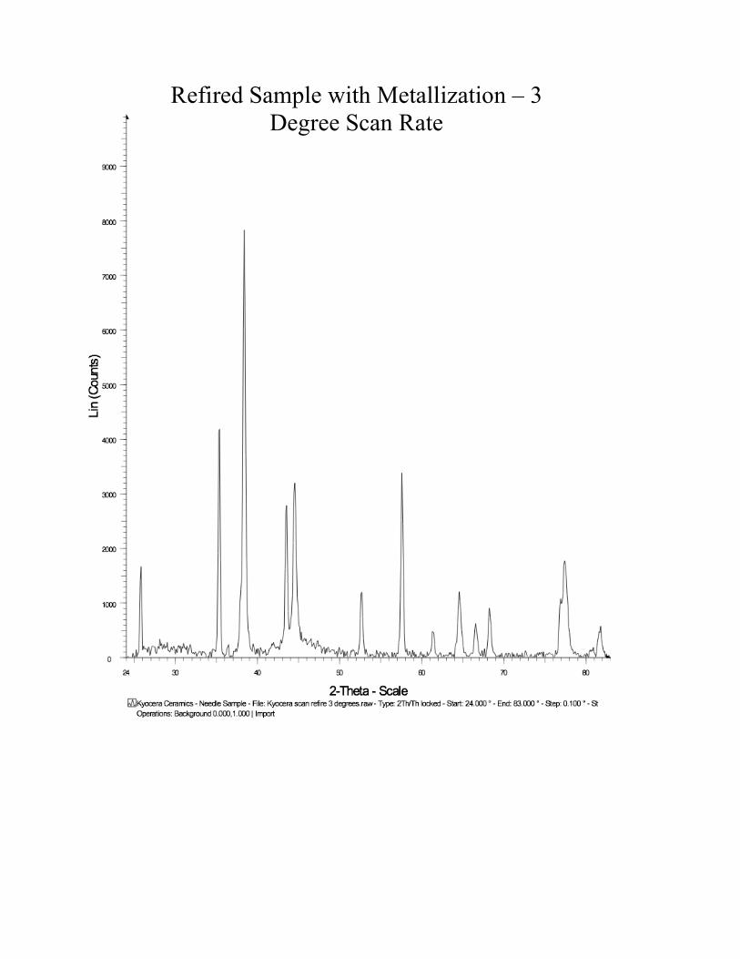
A final XRD scan was run at 1 degree per minute on the sample with the silver
metallization, after the metallization was removed. A comparison was done on the final and
initial scans.
4.0 Results
4.1 X-Ray Diffraction (XRD)
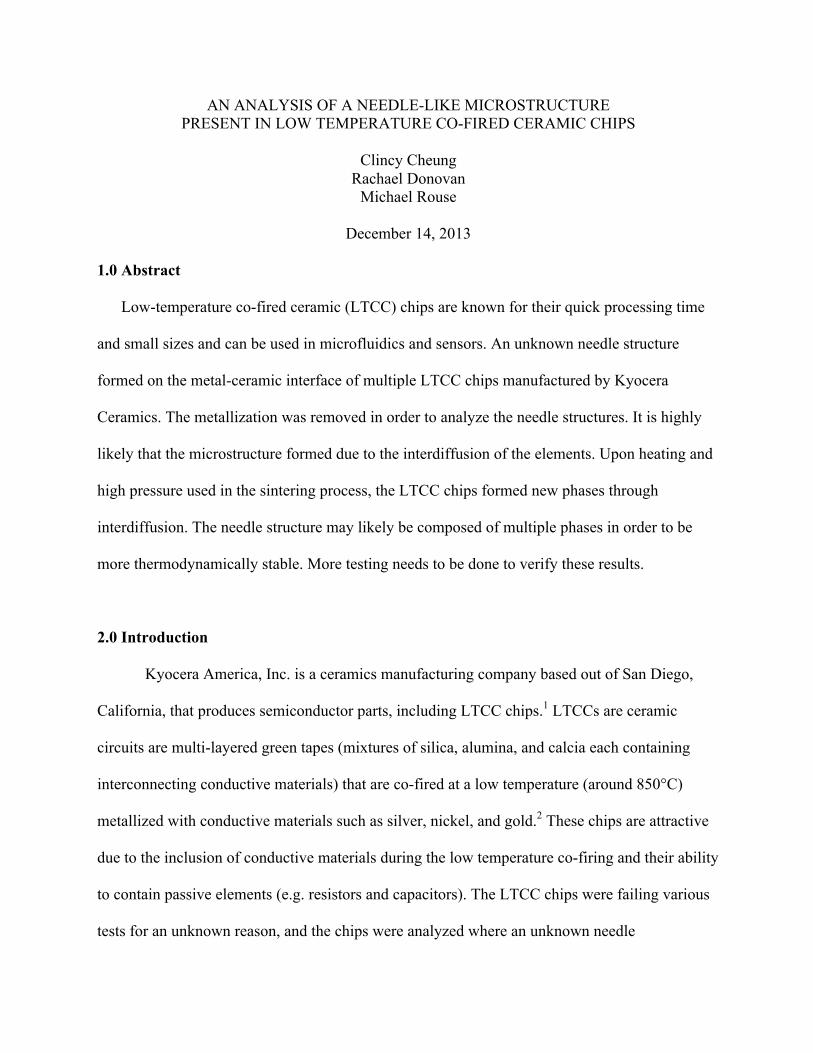
XRD was done on the sample prior to removing the metallization. The results show
corundum, silica, and gold (Figure 1).
Figure 1 – An XRD scan of the LTCC chip with the gold metallization run at 5 degrees per minute from 24 to 80 degrees, showing the presence of silica (green), corundum (blue), and gold (red).
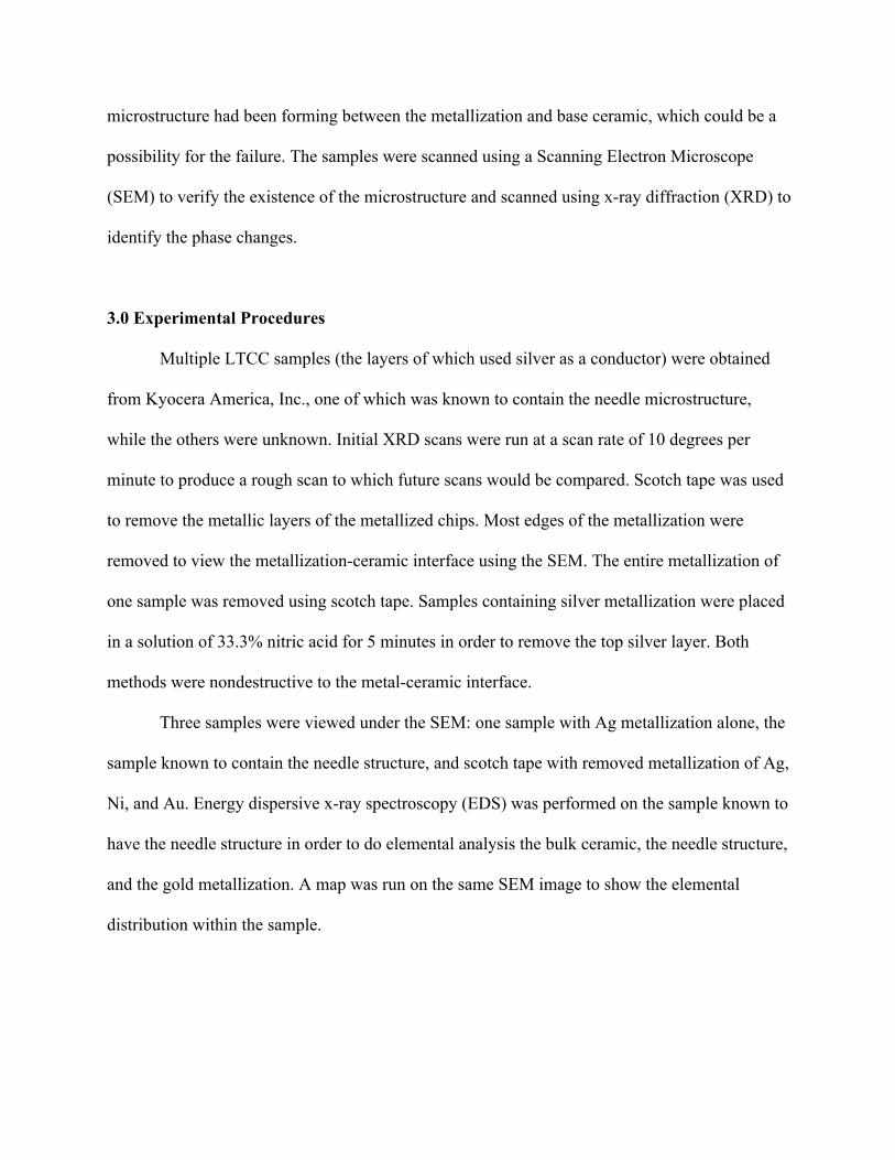
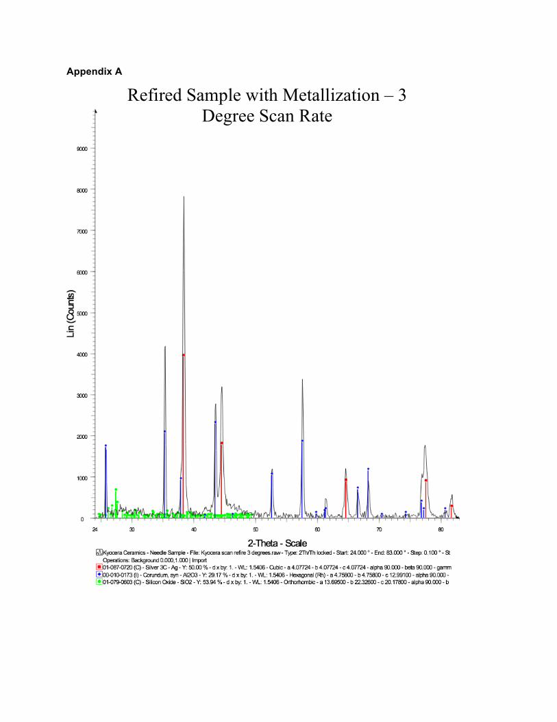
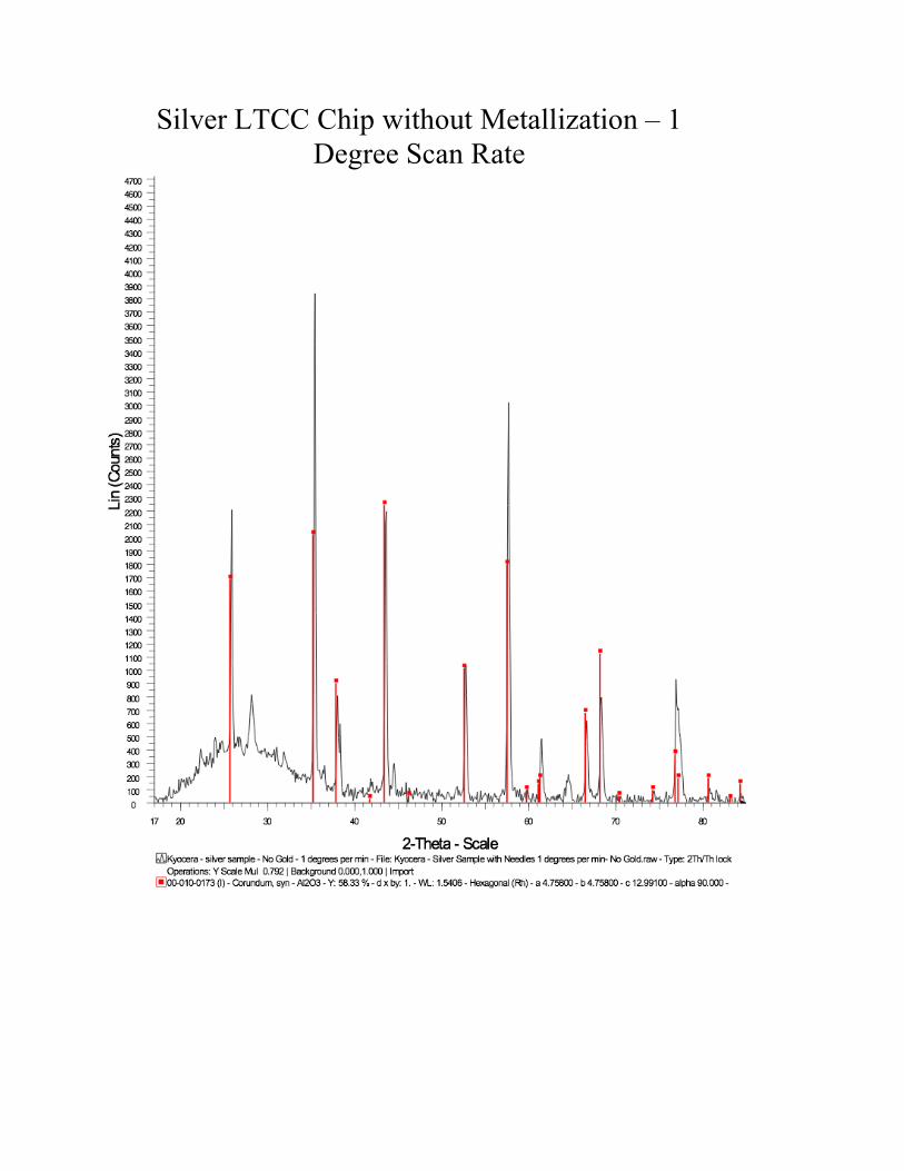
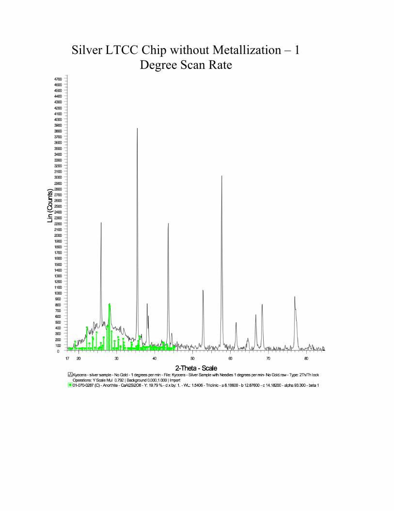
A XRD scan was done to the sample once the metallization was removed. There was a
cluster of new peaks that formed toward the beginning of the scan that verify a new phase or
phases have formed (Figure 2).
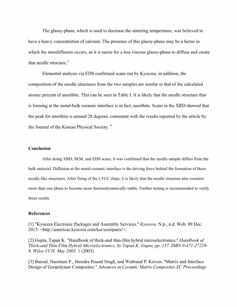
Figure 2 – A XRD scan of the LTCC chip with the metallization removed. There is the possibility of three possible new phases that could be forming: anorthite (red), mordenite (green), and wollastonite (blue).
When comparing these two samples, there is a clear difference between the sample before
and after that can be seen toward the beginning of the scan (Figure 3). The circle area shows the
new peaks that have formed on the sample without the metallization.
Kyocera - silver sample - No Gold - 1 degrees per
01-070-0287 (C) - Anorthite - CaAl2Si2O8 - Y: 18.75 % - d x by: 1. - WL: 1.5406 - Triclinic - a 8.18600 - b 12.87600 - c 14.18200 - alpha 93.300 - beta 101-076-1846 (C) - Wollastonite-2M - Ca3(Si3O9) - Y: 11.74 % - d x by: 1. - WL: 1.5406 - Monoclinic - a 15.33000 - b 7.28000 - c 7.07000 - alpha 90.0001-088-1797 (C) - Mordenite (HCl-treated) - Ca3.6(Al7.2Si40.8O96) - Y: 76.39 % - d x by: 1. - WL: 1.5406 - Orthorhombic - a 18.08900 - b 20.41200 - c Operations: Background 0.031,1.000 | ImportKyocera - silver sample - No Gold - 1 degrees per min - File: Kyocera - Silver Sample with Needles 1 degrees per min- No Gold.raw - Type: 2Th/Th lock
Lin (C
ounts
)
0
1000
2000
3000
4000
5000
2-Theta - Scale17 20 30 40 50 60 70 80
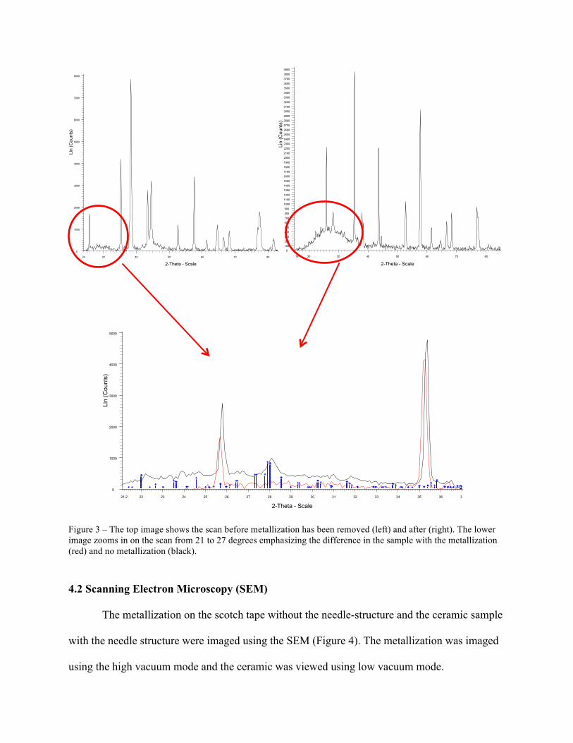
Figure 3 – The top image shows the scan before metallization has been removed (left) and after (right). The lower image zooms in on the scan from 21 to 27 degrees emphasizing the difference in the sample with the metallization (red) and no metallization (black).
4.2 Scanning Electron Microscopy (SEM)
The metallization on the scotch tape without the needle-structure and the ceramic sample
with the needle structure were imaged using the SEM (Figure 4). The metallization was imaged
using the high vacuum mode and the ceramic was viewed using low vacuum mode.
Kyocera Ceramics - Needle Sample
Operations: Background 0.000,1.000 | ImportKyocera Ceramics - Needle Sample - File: Kyocera scan refire 3 degrees.raw - Type: 2Th/Th locked - Start: 24.000 ° - End: 83.000 ° - Step: 0.100 ° - St
Lin
(Cou
nts)
0
1000
2000
3000
4000
5000
6000
7000
8000
9000
2-Theta - Scale24 30 40 50 60 70 80
Kyocera - silver sample - No Gold - 1 degrees per
Operations: Y Scale Mul 0.792 | Background 0.000,1.000 | ImportKyocera - silver sample - No Gold - 1 degrees per min - File: Kyocera - Silver Sample with Needles 1 degrees per min- No Gold.raw - Type: 2Th/Th lock
Lin
(Cou
nts)
0100
200
300400
500
600700
800
900
10001100
1200
13001400
1500
1600
17001800
1900
20002100
2200
23002400
2500
2600
27002800
2900
30003100
3200
3300
34003500
3600
37003800
3900
4000
41004200
4300
44004500
4600
47004800
4900
2-Theta - Scale16 20 30 40 50 60 70 80
Kyocera - silver sample - No Gold - 1 degrees per min
01-070-0287 (C) - Anorthite - CaAl2Si2O8 - Y: 10.42 % - d x by: 1. - WL: 1.5406 - Triclinic - a 8.18600 - b 12.87600 - c 14.18200 - alpha 93.300 - beta 115.790 - gamma 91.120 - Primitive - P-1 (2) - 8 - 1342.Operations: Background 0.081,1.000 | ImportKyocera Ceramics - Refire 3degrees/min - File: Kyocera scan refire 3 degrees per min.raw - Type: 2Th/Th locked - Start: 24.000 ° - End: 83.000 ° - Step: 0.100 ° - Step time: 2. s - Temp.: 25 °C (Room) - TimOperations: Background 0.021,1.000 | ImportKyocera - silver sample - No Gold - 1 degrees per min - File: Kyocera - Silver Sample with Needles 1 degrees per min- No Gold.raw - Type: 2Th/Th locked - Start: 15.000 ° - End: 85.000 ° - Step: 0.100 ° - St
Lin
(Cou
nts)
0
1000
2000
3000
4000
5000
6000
2-Theta - Scale21.2 22 23 24 25 26 27 28 29 30 31 32 33 34 35 36 37
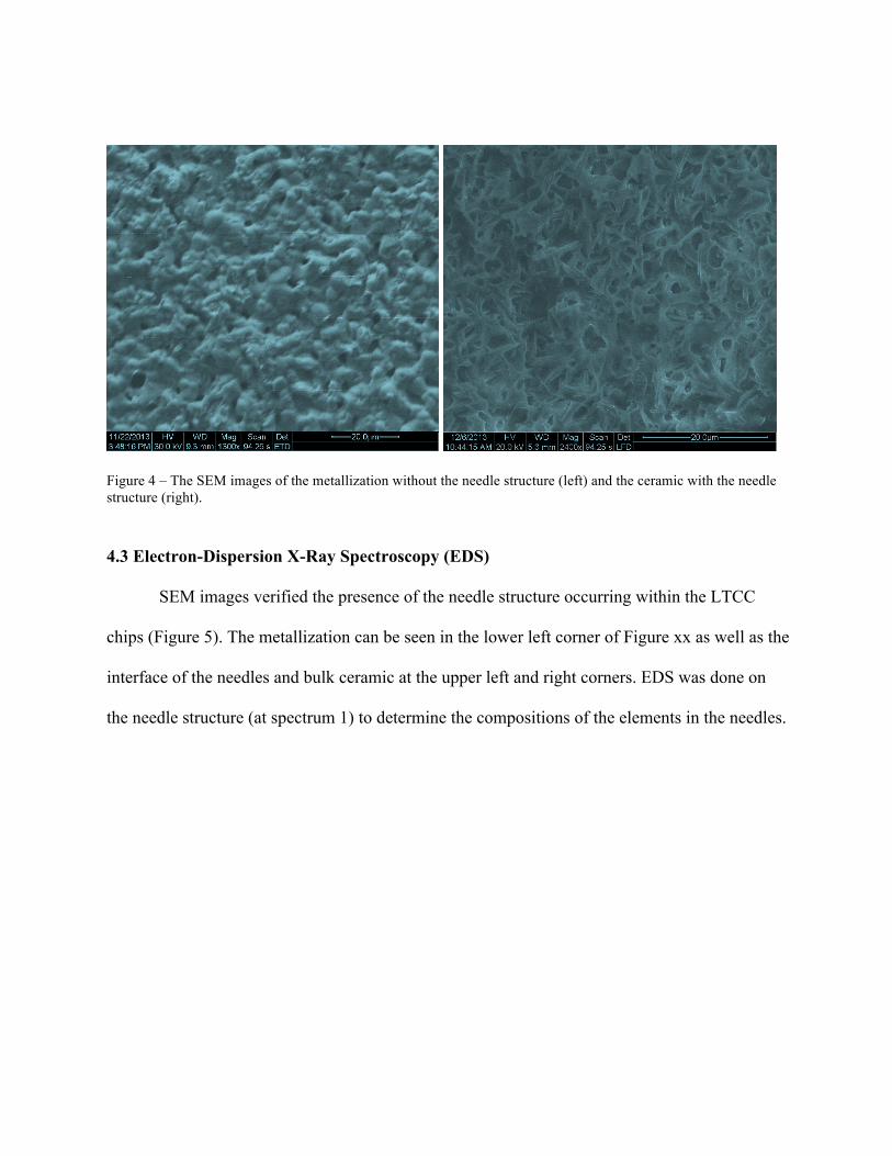
Figure 4 – The SEM images of the metallization without the needle structure (left) and the ceramic with the needle structure (right).
4.3 Electron-Dispersion X-Ray Spectroscopy (EDS)
SEM images verified the presence of the needle structure occurring within the LTCC
chips (Figure 5). The metallization can be seen in the lower left corner of Figure xx as well as the
interface of the needles and bulk ceramic at the upper left and right corners. EDS was done on
the needle structure (at spectrum 1) to determine the compositions of the elements in the needles.

Figure 5 – A micrograph underneath the metallization in an LTCC chip that is known to contain the needle structure. Elemental analysis was done on spectrum 1.
Figure 5 was also scanned using EDS mapping (Figure 6). The different regions are most
distinct within the aluminum map. There is reportedly a high concentration of aluminum in the
bulk ceramic while significantly less within the needle structure and even less so within the
metallization. The main four elements are shown, however there were trace amounts of lead, and
silver, gold and nickel were at the bottom left hand corner, which is to be expected.
Spectrum 1
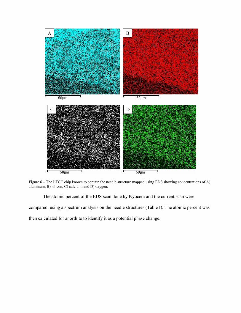
Figure 6 – The LTCC chip known to contain the needle structure mapped using EDS showing concentrations of A) aluminum, B) silicon, C) calcium, and D) oxygen. The atomic percent of the EDS scan done by Kyocera and the current scan were
compared, using a spectrum analysis on the needle structures (Table I). The atomic percent was
then calculated for anorthite to identify it as a potential phase change.
A B
D C
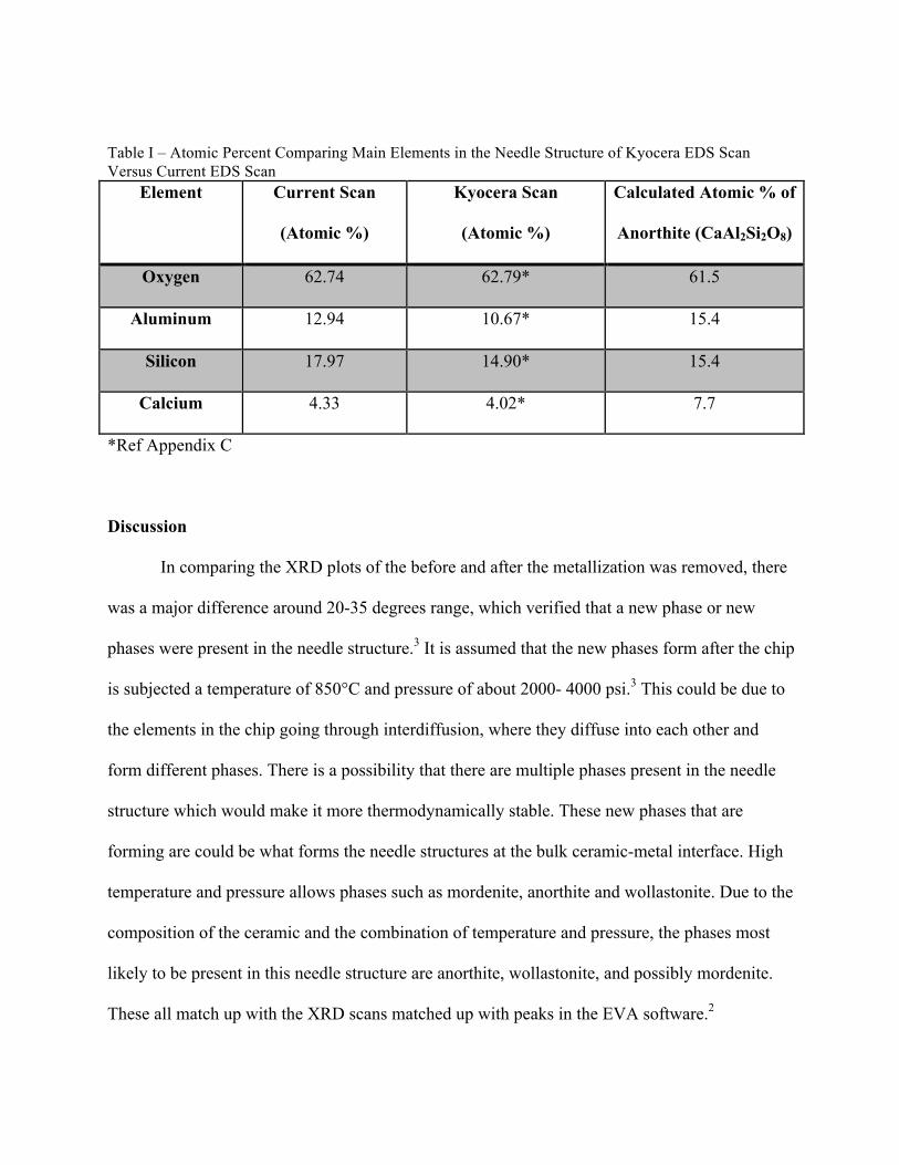
Table I – Atomic Percent Comparing Main Elements in the Needle Structure of Kyocera EDS Scan Versus Current EDS Scan
Element Current Scan
(Atomic %)
Kyocera Scan
(Atomic %)
Calculated Atomic % of
Anorthite (CaAl2Si2O8)
Oxygen 62.74 62.79* 61.5
Aluminum 12.94 10.67* 15.4
Silicon 17.97 14.90* 15.4
Calcium 4.33 4.02* 7.7
*Ref Appendix C
Discussion
In comparing the XRD plots of the before and after the metallization was removed, there
was a major difference around 20-35 degrees range, which verified that a new phase or new
phases were present in the needle structure.3 It is assumed that the new phases form after the chip
is subjected a temperature of 850°C and pressure of about 2000- 4000 psi.3 This could be due to
the elements in the chip going through interdiffusion, where they diffuse into each other and
form different phases. There is a possibility that there are multiple phases present in the needle
structure which would make it more thermodynamically stable. These new phases that are
forming are could be what forms the needle structures at the bulk ceramic-metal interface. High
temperature and pressure allows phases such as mordenite, anorthite and wollastonite. Due to the
composition of the ceramic and the combination of temperature and pressure, the phases most
likely to be present in this needle structure are anorthite, wollastonite, and possibly mordenite.
These all match up with the XRD scans matched up with peaks in the EVA software.2
The glassy-phase, which is used to decrease the sintering temperature, was believed to
have a heavy concentration of calcium. The presence of this glassy-phase may be a factor in
which the interdiffusion occurs, as it is easier for a less viscous glassy-phase to diffuse and create
that needle structure.3
Elemental analysis via EDS confirmed scans run by Kyocera; in addition, the
composition of the needle structures from the two samples are similar to that of the calculated
atomic percent of anorthite. This can be seen in Table I. It is likely that the needle structure that
is forming at the metal-bulk ceramic interface is in fact, anorthite. Scans in the XRD showed that
the peak for anorthite is around 28 degrees, consistent with the results reported by the article by
the Journal of the Korean Physical Society. 4
Conclusion
After doing XRD, SEM, and EDS scans, it was confirmed that the needle sample differs from the
bulk material. Diffusion at the metal-ceramic interface is the driving force behind the formation of these
needle-like structures. After firing of the LTCC chips, it is likely that the needle structure also contains
more than one phase to become more thermodynamically stable. Further testing is recommended to verify
these results.
References [1] "Kyocera Electronic Packages and Assembly Services." Kyocera. N.p., n.d. Web. 09 Dec. 2013. <http://americas.kyocera.com/kai/semiparts/>. [2] Gupta, Tapan K. "Handbook of thick-and thin-film hybrid microelectronics." Handbook of Thick-and Thin-Film Hybrid Microelectronics, by Tapan K. Gupta, pp. 137. ISBN 0-471-27229-9. Wiley-VCH, May 2003. 1 (2003). [3] Bansal, Narottam P., Jitendra Prasad Singh, and Waltraud P. Kriven. "Matrix and Interface Design of Geopolymer Composites." Advances in Ceramic Matrix Composites XI: Proceedings

of the 107th Annual Meeting of the American Ceramic Society : Baltimore, Maryland, USA (2005). Westerville, OH: American Ceramic Society, 2006. 251-60. Print. [4] Zee-Hoon, Park, Park Byung-Ok, Gu Sin-Il, Shin Hyo-Soon, Yeo Dong-Hun, and Kim Jong-Hee. "Microstructure and Crystallinity in a High-Strength LTCC Material of the Anorthite System." Journal of the Korean Physical Society 53.915 (2008): 2467. Print.
Appendix A
Refired Sample with Metallization – 3 Degree Scan Rate
Refired Sample with Metallization – 3 Degree Scan Rate
Silver LTCC Chip without Metallization – 1 Degree Scan Rate

Silver LTCC Chip without Metallization – 1 Degree Scan Rate
Silver LTCC Chip without Metallization – 1 Degree Scan Rate
Silver LTCC Chip without Metallization – 1 Degree Scan Rate

Silver LTCC Chip without Metallization – 1 Degree Scan Rate

Kyocera - silver sample - No Gold - 1 degrees per
01-070-0287 (C) - Anorthite - CaAl2Si2O8 - Y: 18.75 % - d x by: 1. - WL: 1.5406 - Triclinic - a 8.18600 - b 12.87600 - c 14.18200 - alpha 93.300 - beta 101-076-1846 (C) - Wollastonite-2M - Ca3(Si3O9) - Y: 11.74 % - d x by: 1. - WL: 1.5406 - Monoclinic - a 15.33000 - b 7.28000 - c 7.07000 - alpha 90.0001-088-1797 (C) - Mordenite (HCl-treated) - Ca3.6(Al7.2Si40.8O96) - Y: 76.39 % - d x by: 1. - WL: 1.5406 - Orthorhombic - a 18.08900 - b 20.41200 - c Operations: Background 0.031,1.000 | ImportKyocera - silver sample - No Gold - 1 degrees per min - File: Kyocera - Silver Sample with Needles 1 degrees per min- No Gold.raw - Type: 2Th/Th lock
Lin
(Cou
nts)
0
1000
2000
3000
4000
5000
2-Theta - Scale17 20 30 40 50 60 70 80
Silver LTCC Chip without Metallization – 1 Degree Scan Rate

APPENDIX B: SOURCES Matrix and Interface Design of Geopolymer Composites


Low Temperature Co-fired Ceramic (LTCC) Technology: General Processing
Aspects and Fabrication of 3-D Structures for Micro-fluidic Devices
H. Birol, T. Maeder and P. Ryser
Ecole Polytechnique Fédérale de Lausanne (EPFL), Laboratoire de Production de Microtechnique (LPM), CH-1015, Lausanne, Switzerland
Abstract
LTCC technology is based on sintering of multi-layered thick-film sheets (50-250µm) or so-called green tapes, which are screen-printed with thick-film pastes such as conductors, resistors, etc. The terms low temperature and co-fired originate from the relatively low sintering temperatures (<900°C) compared to conventional ceramics and simultaneous firing of tapes together with screen-printed thick-film material, respectively. These characteristics are achieved by improving the tapes’ properties and adopting the physical and chemical thick-film properties to that of tape, whilst retaining their functional properties. Evidently, mastering the technology requires fundamental understanding of the compatibility issues between the tape and the pastes and the effect of processing conditions on this relation. In this perspective, this paper aims to point the origin and extent of chemical and physical interactions between co-fired materials and explain the use of carbon-black sacrificial paste to fabricate 3-D micro-fluidic devices without sagging of the channel walls.
1. Introduction
LTCC technology has recently been one of the most attractive solutions in micro-technology for versatile applications [1]. For a long time, it has been used as the ideal substrate for devices operating at high frequencies, which require faster signal speeds in reduced dimensions. This is facilitated by the low dielectric constant and loss of LTCC tapes, which can be fired at low temperatures with low-resistance conductors (Au, Ag, Cu, etc) at low temperatures. Moreover easy handling of tapes for 3-D structuration, screen-printing with thick-film electronic components, chemical inertness and hermeticity make the technology interesting for other applications such as sensors and micro-fluidics. One of the most cited problems encountered is the incompatibility of the materials used: LTCC tape and thick-film electronic pastes [2]. The LTCC tape usually contains ceramic filler, which is bonded by glass. This glass is used as a sintering aid, which basically reduces the sintering temperature and increases the dielectric strength, and may be formulated to crystallize after sintering to improve stability. The thick-film materials, on the other hand, have different functions and vary in composition. For instance the conductors are metal-based and may contain glass (fritted conductors) and / or oxide additions to increase adhesion to the substrate and enhance sintering, whereas resistors are formed of conducting oxides surrounded by a glass matrix, which determines the resistivity. In either case, glass plays a major role in determining the extent of materials interaction, especially at high temperatures. This arises as a result of the increased mobility of the glass above the glass transition temperature, Tg, which takes place before the densification of the tape/paste. Consequently glass in each component softens over Tg and moves easily due to reduced viscosity, which can lead to chemical and physical incompatibilities in the co-fired module. Chemical issues are best observed using microscopy imaging and measuring functional properties of the components (thermistors / piezo-resistors, conductivity, etc). Additionally chemical analysis such as EDXS (electro dispersive X-ray analysis) provides quantitative information for the chemical interactions occurring between the materials.
Physical issues are detectable rather macroscopically, without a direct need for a microscopic investigation. The differential shrinkage rate between the tape and the pastes, which is observed as warping, curling of the tape, is the major source of physical incompatibility. The deformation arises from different sintering of the pastes prior to

2. Chemical Issues
As explained previously, the glass phase of the fired components plays a major role in the extent of chemical reactions. This is because of the increased diffusion rates of the elements in the softened glass following Tg. Figure 1 shows the difference between heavily fritted (Ag/Pd) and frit-poor (Au) conductor pellets, which are prepared from the powdered-pastes (details of the process in [4]). SEM images illustrate large glass melts in the Ag/Pd conductor and much smaller vitreous regions on the Au matrix. According to the EDXS analysis, the Ag/Pd conductor contains a high glass load of Bi-Zn-Si (~20% atomic), whereas the Au has a trace Bi-Pb-Si load.
Figure 1. SEM images of Ag/Pd (DuPont 9473) and Au (DuPont 5744) conductor pellets.
The LTCC tape-conductor-resistor interface, which is analysed by SEM-imaging the cross-section of the fired structures, is demonstrated in figure 2. It is observed that the Ag/Pd conductor has an open structure forms an extensive reaction zone (RZ) with the LTCC, which is observed in light grey colour. The EDXS analysis carried out in this region shows that it contains elements such as Pb, Bi, which come from the glass phases of the LTCC tape and the conductor, respectively. Additionally needle-like structures are observed, which are found to be Al-Si-rich particles on the RZ. On the other hand, the Au conductor is dense and forms a distinct layer between the tape and the resistor without any further reaction, which is also confirmed by the EDXS analysis. The effect of processing conditions on the extent of reaction can be seen in figure 3, which shows the evolution of the RZ on increased sintering temperature. The thickness of this region increases from 13µm to 16µm and then to 20µm upon increased firing temperature from 850°C to 875°C and then to 900°C.

APPENDIX C