charge equalization based-on three-level npc … · charge equalization based-on three-level npc...
TRANSCRIPT
Charge Equalization Based-on Three-Level NPC Converter for Series Connected Battery Strings
KUEI-HSIANG CHAO1, CHIA-CHANG HSU2 and CHUN-HSIN CHENG2
1Department of Electrical Engineering, National Chin-Yi University of Technology 35, Lane 215, Sec. 1, Chung-Shan Road, Taiping City, Taichung County
TAIWAN, R.O.C. [email protected]
2Institute of Information and Electrical Energy, National Chin-Yi University of Technology
Abstract: - The main purpose of this paper is to design a charge equalization circuit for series connected lead-acid batteries. The charger utilizes a three-level neutral point clamped (NPC) AC/DC converter with voltage balance control to charge the series connected rechargeable battery strings. This paper details the operation principles of the charge equalization circuit under different operation modes and derives the governed equations. The proposed charge equalization circuit can not only regulate the power factor of AC source side, but also can balance the charge voltage for series connected rechargeable batteries. Finally, some simulation results are made to demonstrate the effectiveness of the charge equalization circuit scheme presented in this paper.
Key-Words: Lead-Acid Battery, Charge Equalization Circuit, Three-Level Converter, Voltage Balance Control, Neutral Point Clamped (NPC) Converter.
1 Introduction Lead-acid batteries play an important role in human life. In recent years, the demand for lead-acid batteries has increased due to energy shortages and problems of environmental pollution. However, as single rechargeable batteries cannot satisfy the electrical demands of many systems, generally multiple batteries are series connected into a battery pack in order to provide sufficient voltage. Nevertheless, when multiple rechargeable batteries are series connected for recharging, imbalances result in the amounts of electricity charged into the batteries due to differences in internal characteristics, and chemical components between the batteries involved. Consequently, as the number of batteries series connected in a battery pack increases, the lifespan of the batteries will decrease exponentially [1,2]. The main purpose of battery chargers is to create an equivalent state-of-charge (SOC) in each battery in a series connected battery pack. When there are unequal charges between batteries in a battery pack, high capacity batteries require less energy for recharging, while lower capacity rechargeable batteries require higher energies for recharging in order to meet the equivalent charging needs of battery packs.
Current research on charge equalization technologies can be broadly divided into extended time overcharging, consumable charge equalization scheme, inductor charge equalization scheme, switched capacitor charge equalization system, and
multi-winding transformer charge equalization scheme [3-10]. The extended time overcharging method [3] involves extending the charging times for series connected battery packs. Battery packs that generally require only 12 hours for charging have their charging times extended in order to ensure that every battery within the pack is highly charged and to allow the lowest-capacity battery to meet high-capacity needs. However, this method leads to the risk of gas seepage in higher-capacity batteries. Consumable charge equalization schemes [4] connect a charge equalizer to each battery in a battery pack. These equalizers are generally composed of resistors, zener diodes, and voltage controlled current elements. When any battery in the pack exceeds a set voltage, the equalizers are activated and redirect a portion of the charging current to the equalizer, thereby reducing current flow to batteries and preventing the occurrence of overcharging. However, this method wastes a significant amount of energy on equalizers and leads to unnecessary energy loss. Inductor charge equalization schemes [5] are divided into forward and backward charge equalization schemes. The operation principle of inductor charge equalization scheme is to use switches and inductors of charge equalization sub-circuits to transfer energy of high-capacity batteries, causing the battery energies of every battery in a pack to be equalized. The shortcoming of this method is that the energy transfer is limited by the capacity of the inductors, which may lead to overly long charging times. Capacitor charge equalization schemes [6] connect linked battery packs
WSEAS TRANSACTIONS on CIRCUITS and SYSTEMS Kuei-Hsiang Chao, Chia-Chang Hsu, Chun-Hsin Cheng
ISSN: 1109-2734 863 Issue 11, Volume 8, November 2009
to a scheme consisting of bi-direction switches and capacitors. This scheme switches rapidly between switches and capacitors to transfer unequal energy between batteries, thereby reducing power difference between batteries and attaining the goal of equal charging. The shortcomings of this method are that energy transfer is limited by the energy storage capacities of the capacitors and that excessively long equal charging times may be produced. The operation principle of multi-winding transformer charge equalization schemes [7-10] lies in using DC-DC converters to charge series connected battery packs at the high-charging rate when the series connected battery packs are in a low-power state at the beginning of the charging process; when the set voltage has been reached, the batteries are switched to charging under a charge equalization mode. The charge equalization circuits of this scheme consist of a set of multi-winding transformers and a DC-DC converter. As the series connected battery packs charge each battery at identical voltages on the secondary side, the batteries are charged at identical voltages; higher-capacity batteries are charged at lower charging rates, while relatively lower-capacity batteries are charged at higher rates. Consequently, over a period of time, the capacities in each battery in a series connected battery pack will be balanced, thereby reaching the effect of charge equalization. This type of scheme faces the issues of mutual inductance and leakage inductance between mutually coupled windings. As a result, even with equal numbers of winding turns, identical charge voltages cannot be obtained.
This study presents the use of a three-level neutral point clamped AC/DC converter to directly perform constant voltage charging in order to overcome the problems with existing rechargeable battery charge equalization circuits. Not only can the converters and their control schemes cause the power factor for the AC input side to approach 1, it can also rapidly complete equal charging for series connected battery packs. 2 Three-Level Neutral Point Clamped
Converter Charge Equalization Scheme
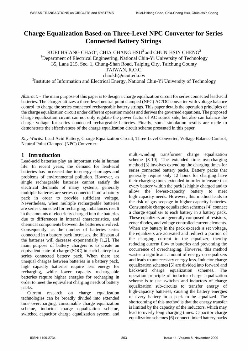
Figure 1 depicts the proposed neutral point voltage balance control three-level AC/DC converter charge equalization scheme that possesses power factor correction. So that the power voltage will obtain three-level voltage wave forms every 1 1/2 cycles, we use eight IGBT power semiconductors 1 8S S− as power switches and the neutral point clamped rectifier composed of four clamped diodes 1 4D D−
[11-13]. A boosting inductor sL is connected to the AC side as a storage inductor for power factor control; the DC side of the converter is connected to the serial battery strings, so that through the DC voltage controller, a stable DC voltage can be provided to charge the series connected battery pack. In order for the power factor of the input end to approach 1.0, the errors of DC feedback voltage '
dcV = v dcK V ( vK is the sensed voltage factor ) and command voltage *
dcV produce the peak value command *
acI of the input current after being regulated by the voltage controller. This value multiplied by the unit sine wave ( )S tω with the same phase as the input voltage acv produces the input current command *
aci . Thereafter, a hysteresis current controller (HCC) is used to produce the switching control signal for the power semiconductor, thereby causing the actual input current '
ac s aci K i= ( sK is the sensed current factor) closely following command current *
aci , causing the power factor of the AC input side to approach 1. 3 Operation Principles of the Charge
Equalizer We first make the following four assumptions to analyze this charge equalization circuit for rechargeable batteries: (1)assume that all components are ideal and do not suffer from voltage drop or switching loss; (2)the characteristics of the two rechargeable batteries are identical; (3)within a short switching period, input AC voltage can be viewed as a constant value; (4)AC line resistance sR can be ignored. For this converter, there are three possible switching states, 1 2 1S S= = ( 5 6 1S S= = ), 2 3 1S S= = ( 6 7 1S S= = ), and 3 4 1S S= = ( 7 8 1S S= = ). Consequently, there are 23 9= possible changes in switching modes for the three-level neutral point clamped converter switch. Three of these modes can produce zero voltage at the input end voltage abv . To save on switching states, only 2 3 6 7 1S S S S= = = = zero voltage switching mode was selected. Thus, seven possible switch switching modes remain; these modes can produce five types of voltage ( 0 , 2dcV± , dcV± ) levels at AC side input voltage abv . If the three-level input voltage wave form is to be obtained, the relationship between electrical input voltage acv and DC output voltage must meet the condition of ,2dc ac peak dcV v V< < . Consequently, we first designate 2ac dcv V<| | as Area 1 and designate
2ac dcv V>| | as Area 2; we assume that
WSEAS TRANSACTIONS on CIRCUITS and SYSTEMS Kuei-Hsiang Chao, Chia-Chang Hsu, Chun-Hsin Cheng
ISSN: 1109-2734 864 Issue 11, Volume 8, November 2009
1 2 2B B dcv v V= = .
Fig. 1 The scheme of three-level NPC AC/DC converter charge equalizer with power factor correction
If the three-level AC/DC converter is operated at forward power transmission, it can be divided into seven different operation modes for analysis. The circuit configurations for the various modes are as shown in Figs. 2 through 8; the corresponding switch state, input voltage, input current, and charging and discharging state of the battery pack are shown in Table 1. The circuit operations of the various operating modes are described below.
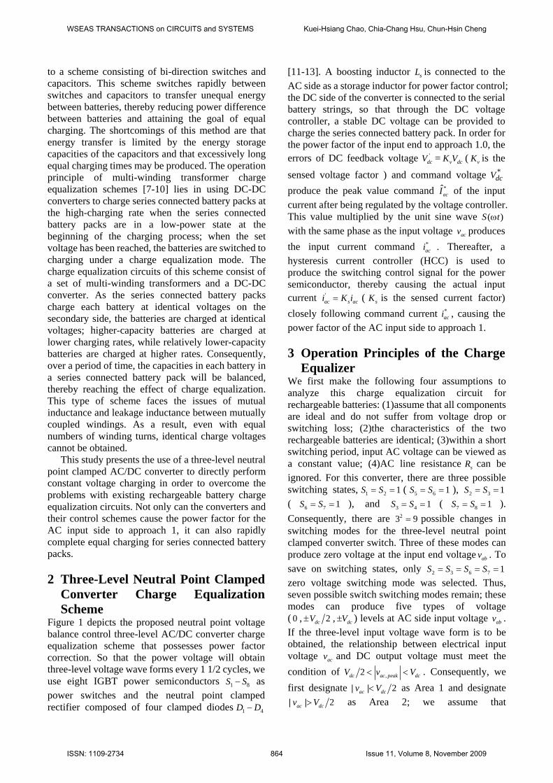
(1) Mode 1 Power semiconductor switches 1S , 2S , 7S , and 8S
are triggered; the circuit configuration is as shown in Fig. 2. At this instant, line current aci flows towards boost inductor sL , travels through the anti-parallel diodes of switches 2S and 1S , batteries 1B and 2B , and the anti-parallel diode of switch 8S , then finally returns to the electrical supply terminal through the anti-parallel diode of switch 7S . In this mode, the input terminal voltage of the converter is ab dcv V=
( 1 2B Bv v= + ). Since the electrical supply voltage 0acv > and its amplitude is within Area 2, the line
current aci decreases. At this instant, the circuit equation can be expressed as:
1 2ac
ac s B Bdi
v L v vdt
= + + (1)
1Bi
acv
SL
1S
2S
5S
3S
6S
7S
8S4S
dcV+
−
aci
1D
2D
3D
4D
abv+
−
N
a
b
SR
2Bi
B
B
1
2
+
+
−
−
v
v
B1
B2
+
−
Fig. 2 Circuit for mode 1 of the three-level neutral point clamped charge converter
WSEAS TRANSACTIONS on CIRCUITS and SYSTEMS Kuei-Hsiang Chao, Chia-Chang Hsu, Chun-Hsin Cheng
ISSN: 1109-2734 865 Issue 11, Volume 8, November 2009
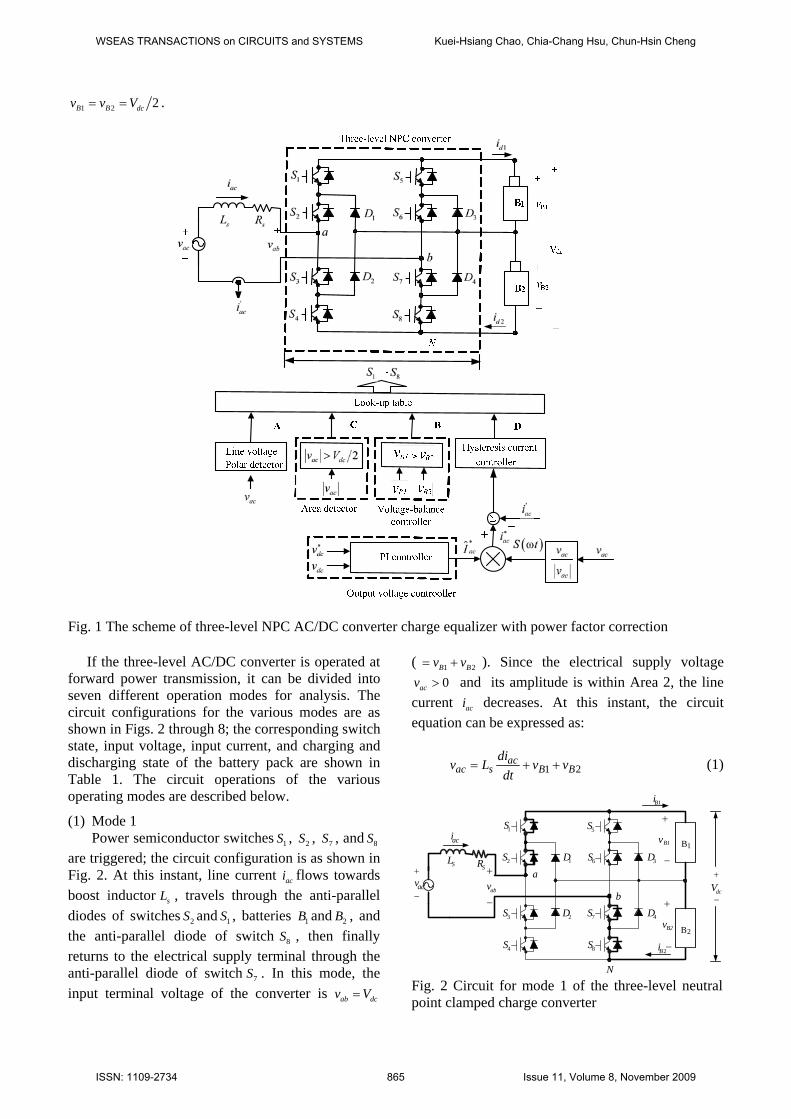
(2) Mode 2 Power semiconductor switches 1S , 2S , 6S , and 7S
are triggered; the circuit configuration is as shown in Fig. 3. At this instant, line current aci flows towards boost inductor sL , passes through the anti-parallel diodes of switches 2S and 1S , battery 1B , clamped diode 3D , and then finally returns to the power source terminal through switch 6S . In this mode, the input terminal voltage of the converter is 2ab dcv V= ( 1Bv= ). If the power source voltage 0acv > and its amplitude is within Area 2, then the line current aci will increase. However, if the power source voltage 0acv > and the amplitude is within Area 1, then the line current
aci will decrease. In this interval, the circuit equation can be written as:
1ac
ac s Bdi
v L vdt
= + (2)
1Bi
acv
SL
1S
2S
5S
3S
6S
7S
8S4S
dcV+
−
aci
1D
2D
3D
4D
abv+
−
N
a
b
SR
2Bi
B
B
1
2
+
+
−
−
v
v
B1
B2
+
−
Fig. 3 Circuit for mode 2 of the three-level neutral point clamped charge converter (3) Mode 3
Power semiconductor switches 2S , 3S , 7S , and 8S are triggered. At this time, the line current aci flows
towards boost inductor sL , passing through switch 3S , clamped diode 2D , battery 2B , and the anti-parallel diode of switch 8S , then finally returns to the power source terminal through the anti-parallel diode of switch 7S . The circuit configuration is as shown in Fig. 4. In this mode, the input terminal voltage of converter is 2ab dcv V= ( 2Bv= ). If the power source voltage 0acv > and its amplitude is within Area 2, then the line current aci rises. However, if power source voltage 0acv > and the amplitude is within Area 1, then the line current aci drops. At this instant, the circuit equation can be expressed as:
2ac
ac s Bdi
v L vdt
= + (3)
1Bi
acv
SL
1S
2S
5S
3S
6S
7S
8S4S
dcV+
−
aci
1D
2D
3D
4D
abv+
−
N
a
b
SR
2Bi
B
B
1
2
+
+
−
−
v
v
B1
B2
+
−
Fig. 4 Circuit for mode 3 of the three-level neutral point clamped charge converter (4) Mode 4
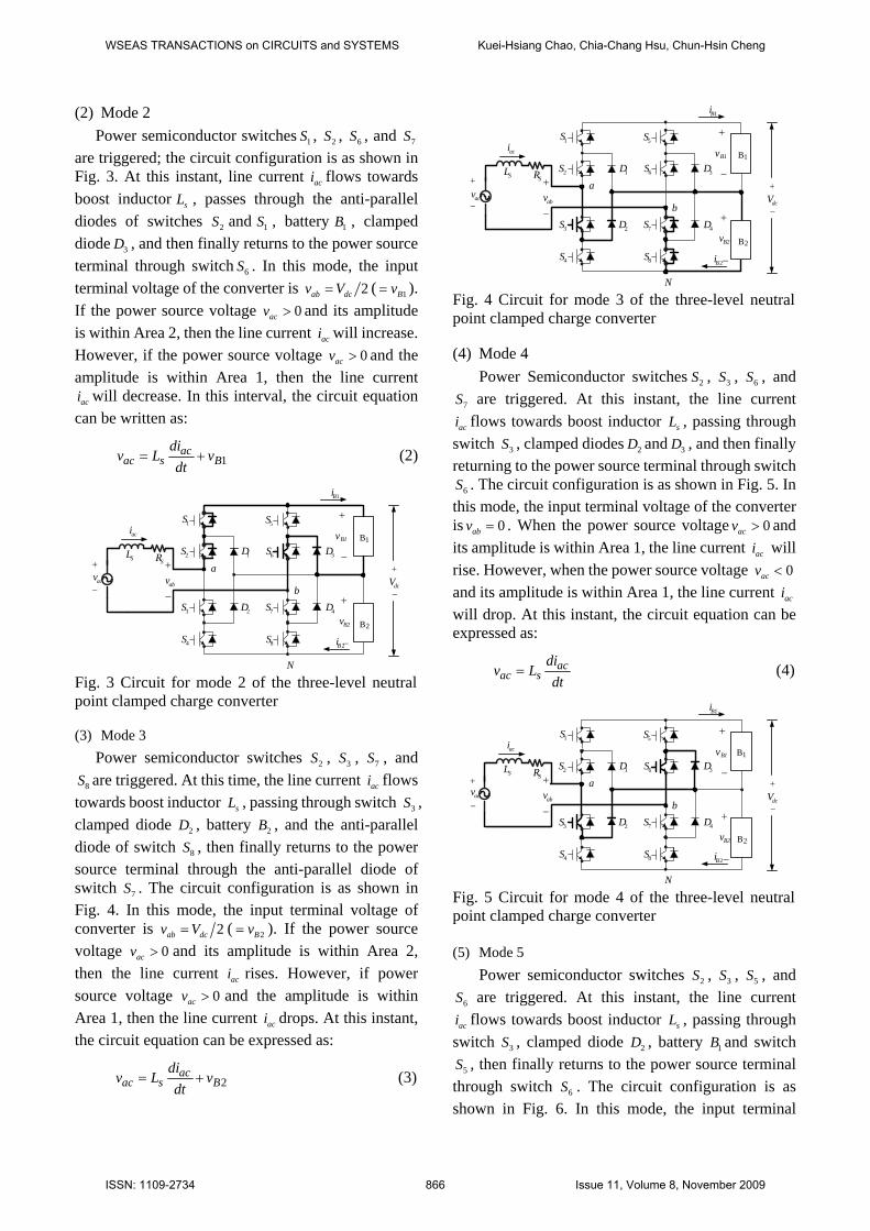
Power Semiconductor switches 2S , 3S , 6S , and 7S are triggered. At this instant, the line current
aci flows towards boost inductor sL , passing through switch 3S , clamped diodes 2D and 3D , and then finally returning to the power source terminal through switch
6S . The circuit configuration is as shown in Fig. 5. In this mode, the input terminal voltage of the converter is 0abv = . When the power source voltage 0acv > and its amplitude is within Area 1, the line current aci will rise. However, when the power source voltage 0acv < and its amplitude is within Area 1, the line current aci will drop. At this instant, the circuit equation can be expressed as:
acac s
div L
dt= (4)
1Bi
acv
SL
1S
2S
5S
3S
6S
7S
8S4S
dcV+
−
aci
1D
2D
3D
4D
abv+
−
N
a
b
SR
2Bi
B
B
1
2
+
+
−
−
v
v
B1
B2
+
−
Fig. 5 Circuit for mode 4 of the three-level neutral point clamped charge converter (5) Mode 5
Power semiconductor switches 2S , 3S , 5S , and 6S are triggered. At this instant, the line current
aci flows towards boost inductor sL , passing through switch 3S , clamped diode 2D , battery 1B and switch
5S , then finally returns to the power source terminal through switch 6S . The circuit configuration is as shown in Fig. 6. In this mode, the input terminal
WSEAS TRANSACTIONS on CIRCUITS and SYSTEMS Kuei-Hsiang Chao, Chia-Chang Hsu, Chun-Hsin Cheng
ISSN: 1109-2734 866 Issue 11, Volume 8, November 2009
voltage of the converter is 2ab dcv V= − ( 1Bv= − ). When the power source voltage 0acv < and its amplitude is within Area 1, the line current aci rises; when the power source voltage 0acv < and its amplitude is within Area 2, line current aci drops. At this time, the circuit equation can be expressed as:
1ac
ac s Bdi
v L vdt
= − (5)
1Bi
acv
SL
1S
2S
5S
3S
6S
7S
8S4S
dcV+
−
aci
1D
2D
3D
4D
abv+
−
N
a
b
SR
2Bi
B
B
1
2
+
+
−
−
v
v
B1
B2
+
−
Fig. 6 Circuit for mode 5 of the three-level neutral point clamped charge converter (6) Mode 6
Power Semiconductor switches 3S , 4S , 6S , and 7S are triggered. At this instant, line current aci flows towards boost inductor sL , passing through switches
3S and 4S , battery 2B , and clamped diode 3D , and then finally returns to the power source terminal through switch 6S . The circuit configuration is as shown in Fig. 7. In this mode, the input terminal voltage of the converter is 2ab dcv V= − ( 2Bv= − ). When the power source voltage 0acv < and its amplitude is within Area 1, the line current aci rises; when power source voltage 0acv < and its amplitude is within Area 2, the line current aci drops. At this instant, the circuit equation can be expressed as:
2ac
ac s Bdi
v L vdt
= − (6)
1Bi
acv
SL
1S
2S
5S
3S
6S
7S
8S4S
dcV+
−
aci
1D
2D
3D
4D
abv+
−
N
a
b
SR
2Bi
B
B
1
2
+
+
−
−
v
v
B1
B2
+
−
Fig. 7 Circuit for mode 6 of the three-level neutral point clamped charge converter
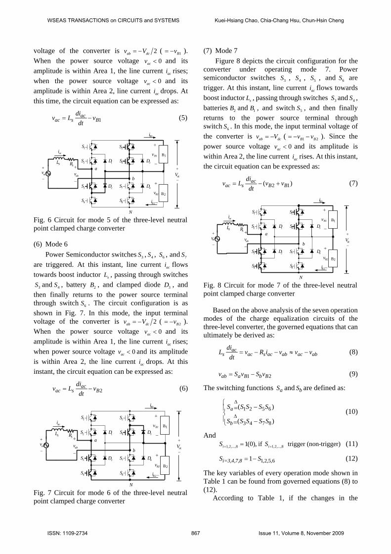
(7) Mode 7 Figure 8 depicts the circuit configuration for the
converter under operating mode 7. Power semiconductor switches 3S , 4S , 5S , and 6S are trigger. At this instant, line current aci flows towards boost inductor sL , passing through switches 3S and 4S , batteries 2B and 1B , and switch 5S , and then finally returns to the power source terminal through switch 6S . In this mode, the input terminal voltage of the converter is ab dcv V= − ( 1 2B Bv v= − − ). Since the power source voltage 0acv < and its amplitude is within Area 2, the line current aci rises. At this instant, the circuit equation can be expressed as:
2 1( )acac s B B
div L v v
dt= − + (7)
1Bi
acv
SL
1S
2S
5S
3S
6S
7S
8S4S
dcV+
−
aci
1D
2D
3D
4D
abv+
−
N
a
b
SR
2Bi
B
B
1
2
+
+
−
−
v
v
B1
B2
+
−
Fig. 8 Circuit for mode 7 of the three-level neutral point clamped charge converter
Based on the above analysis of the seven operation modes of the charge equalization circuits of the three-level converter, the governed equations that can ultimately be derived as:
acs ac s ac ab ac ab
diL v R i v v v
dt= − − ≈ − (8)
1 2ab a B b Bv S v S v= − (9)
The switching functions aS and bS are defined as:
1 2 5 6
3 4 7 8
( )
( )
a
b
S S S S S
S S S S S
Δ
Δ
⎧ −=⎪⎨⎪ −=⎩
(10)
And 1,2,...,8 1,2,...,81(0), if trigger (non-trigger)i iS S= == (11)
1,2,5,61i=3,4,7,8S S= − (12)
The key variables of every operation mode shown in Table 1 can be found from governed equations (8) to (12).
According to Table 1, if the changes in the
WSEAS TRANSACTIONS on CIRCUITS and SYSTEMS Kuei-Hsiang Chao, Chia-Chang Hsu, Chun-Hsin Cheng
ISSN: 1109-2734 867 Issue 11, Volume 8, November 2009
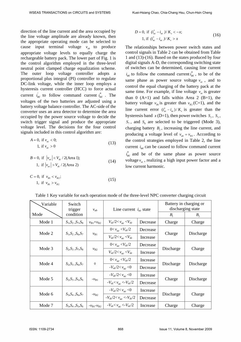
direction of the line current and the area occupied by the line voltage amplitude are already known, then the appropriate operating mode can be selected to cause input terminal voltage abv to produce appropriate voltage levels to equally charge the rechargeable battery pack. The lower part of Fig. 1 is the control algorithm employed in the three-level neutral point clamped charge equalization scheme. The outer loop voltage controller adopts a proportional plus integral (PI) controller to regulate DC-link voltage, while the inner loop employs a hysteresis current controller (HCC) to force actual current '
aci to follow command current *aci . The
voltages of the two batteries are adjusted using a battery voltage balance controller. The AC-side of the converter uses an area detector to determine the area occupied by the power source voltage to decide the switch trigger signal and produce the appropriate voltage level. The decisions for the four control signals included in this control algorithm are:
0, if 0; 1, if 0
ac
ac
A vv
= <
> (13)
0, if / 2(Area 1);
1, if / 2(Area 2)ac dc
ac dc
B v V
v V
= <
> (14)
1 2
1 2
0, if ; 1, if
B B
B B
C v vv v
= <>
(15)
*
*
0, if / ;
1, if /ac ac s
ac ac s
D (i i ) K x
(i i ) K x
= − < −
− > (16)
The relationships between power switch states and control signals in Table 2 can be obtained from Table 1 and (13)-(16). Based on the states produced by four digital signals A-D, the corresponding switching state of switches can be determined, causing line current
aci to follow the command current *aci , to be of the
same phase as power source voltage acv , and to control the equal charging of the battery pack at the same time. For example, if line voltage acv is greater than 0 (A=1) and falls within Area 2 (B=1), the battery voltage 1Bv is greater than 2Bv (C=1), and the line current error ( ) /ac ac si i K∗ − is greater than the hysteresis band x (D=1), then power switches 2S , 3S ,
7S , and 8S are selected to be triggered (Mode 3), charging battery 2B , increasing the line current, and producing a voltage level of 2ab Bv v= . According to the control strategies employed in Table 2, the line current aci can be caused to follow command current
*aci and be of the same phase as power source
voltage acv , realizing a high input power factor and a low current harmonic.
Table 1 Key variable for each operation mode of the three-level NPC converter charging circuit
Variable
Mode
Switch trigger
condition vab Line current iac state
Battery in charging or discharging state
1B 2B
Mode 1 S1,S2 ,S7,S8 vB1+vB2 Vdc/2< acv <Vdc Decrease Charge Charge
Mode 2 S1,S2 ,S6,S7 vB1 0< acv <Vdc/2 Decrease
Charge Discharge Vdc/2< acv <Vdc Increase
Mode 3 S2,S3 ,S7,S8 vB2 0< acv <Vdc/2 Decrease
Discharge Charge Vdc/2< acv <Vdc Increase
Mode 4 S2,S3 ,S6,S7 0 0< acv <Vdc/2 Increase
Discharge Discharge -Vdc/2< acv <0 Decrease
Mode 5 S2,S3 ,S5,S6 -vB1 -Vdc/2< acv <0 Increase
Charge Discharge -Vdc< acv <-Vdc/2 Decrease
Mode 6 S3,S4 ,S6,S7 -vB2 -Vdc/2< acv <0 Increase
Discharge Charge -Vdc/2< acv <-Vdc/2 Decrease
Mode 7 S3,S4 ,S5,S6 -vB1-vB2 -Vdc< acv <-Vdc/2 Increase Charge Charge
WSEAS TRANSACTIONS on CIRCUITS and SYSTEMS Kuei-Hsiang Chao, Chia-Chang Hsu, Chun-Hsin Cheng
ISSN: 1109-2734 868 Issue 11, Volume 8, November 2009

4 Simulation Results Figure 9(a) shows the simulated circuit of the proposed three-level neutral point clamped AC/DC converter for equalization charge two series connected batteries. The number of required components for the simulated circuit of the three-level neutral point clamped AC/DC converter charge equalizer can be obtained through the following formulas [11]: the formula ( 1) 2 (m m− × is the number of levels) obtains the number of power semiconductor switches need for each leg of bridge converter, while the formula ( 1) ( 2)m m− × − obtains the number of neutral point clamped diodes needed for each leg of bridge converter. For example, for a three-level converter, there will be 8 IGBT power semiconductor switches and 4 neutral point clamped diodes composing the circuit scheme. Figure 9(b) is the sub-circuit diagram for the lead-acid batteries in the simulated circuit diagram of the three-level neutral
point clamped circuit using PSIM software [14]. Figure 10 (a) is the simulated circuit for the
controller of the three-level neutral point clamped charge equalizer. The parameter settings for the outer loop voltage controller are 01.0=PK and 035.0=IK ; the power source terminal resistance is 5sR m= Ω , the power source terminal inductor is 0.175sL mH= , the power source voltage is 14acv V= , and the DC link output voltage is 28dcV V= ; the battery is a 12V-13Ah battery. The inner loop produces an A-D digital signal through comparison, and then uses the relationship between the switching functions of power switches and control signals, writing the relationship as C-code and using a complier to produce the dynamic link library (DLL) needed for the PSIM circuit simulation software [15]. Figure 10 (b) is the switch control decision established in Table 2 used to decide the operating mode of the switches.
(a)
(b)
Fig. 9 Simulated circuit diagrams using PSIM software for the three-level neutral point clamped converter charger equalization circuit: (a)main circuit scheme; (b)sub-circuit of lead-acid batteries
WSEAS TRANSACTIONS on CIRCUITS and SYSTEMS Kuei-Hsiang Chao, Chia-Chang Hsu, Chun-Hsin Cheng
ISSN: 1109-2734 869 Issue 11, Volume 8, November 2009
VB1
B2V
(a)
(b)
Fig. 10 Control circuit diagrams using PSIM software for the three-level neutral point clamped converter charge equalization circuit: (a)voltage controller; (b)switching controller of digital signal
Table 2 Relations between control signals and switching functions of power switches in each mode
A B C D 1S
( 3S )
2S
( 4S )
5S
( 7S )
6S
( 8S )
Operation Mode
0 0 0 0 0 1 0 1 4 0 0 0 1 0 1 1 1 5 0 0 1 0 0 1 0 1 4 0 0 1 1 0 0 0 1 6 0 1 0 0 0 1 1 1 5 0 1 0 1 0 0 1 1 7 0 1 1 0 0 0 0 1 6 0 1 1 1 0 0 1 1 7 1 0 0 0 1 1 0 1 2 1 0 0 1 0 1 0 1 4 1 0 1 0 0 1 0 0 3 1 0 1 1 0 1 0 1 4 1 1 0 0 1 1 0 0 1 1 1 0 1 1 1 0 1 2 1 1 1 0 1 1 0 0 1 1 1 1 1 0 1 0 0 3
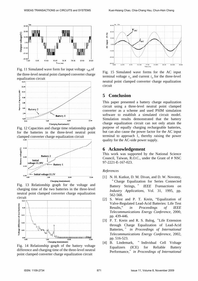
Figure 11 shows the simulated wave form of the input terminal voltage abv for the three-level NPC converter equalization equal charger, it can be seem
from simulation results that abv has three levels at positive and negative half cycles and can thus reduce output voltage harmonics. Figure 12 shows the change curves for the capacities of the two batteries during charging. The initial voltages and capacities of the two batteries were set differently at the start of the simulation. The voltage of Battery 1 was initially set at 11.1V, while the voltage of Battery 2 was initially set as 11.39V. In the charging period (at 3 minutes), the capacity of Battery 2 was increased to exacerbate the inequality in the capacities of lead-acid batteries. The simulation results shown in Fig. 12 indicate that the charge equalization circuit does indeed have good equal charging effects. Figure 13 shows the voltage changes in the two batteries during the charging period, while Fig. 14 shows the voltage differences between the two batteries. Fig. 15 shows the simulated wave forms for input AC voltage acv and current aci during the charging period. It can be seen from the simulation results shown in Figs. 13-15 that the three-level converter charger equalization circuit possesses excellent performance in providing battery packs with equal charging and can improve the power quality of the charging power source.
WSEAS TRANSACTIONS on CIRCUITS and SYSTEMS Kuei-Hsiang Chao, Chia-Chang Hsu, Chun-Hsin Cheng
ISSN: 1109-2734 870 Issue 11, Volume 8, November 2009
Out
put v
olta
ge(V
)
Fig. 11 Simulated wave form for input voltage vab of the three-level neutral point clamped converter charge equalization circuit
Fig. 12 Capacities and charge time relationship graph for the batteries in the three-level neutral point clamped converter charge equalization circuit
11.00
11.50
12.00
12.50
13.00
0.00 5.00 10.00 15.00
Charging time(minute)
Bat
tery
vol
tage
(V)
Battery 1
Battery 2
Initial voltage:11.1V
Initial voltage:11.39V
Fig. 13 Relationship graph for the voltage and charging time of the two batteries in the three-level neutral point clamped converter charge equalization circuit
0.25
0.20
0.15
0.10
0.05
0.000.00 5.00 10.00 15.00
Vol
tage
diff
eren
ce o
f tw
o ba
tter
ies
Charging time(minute)
Fig. 14 Relationship graph of the battery voltage difference and charging time of the three-level neutral point clamped converter charge equalization circuit
vac
iac
AC
inpu
t(V
/A)
Fig. 15 Simulated wave forms for the AC input terminal voltage acv and current aci for the three-level neutral point clamped converter charge equalization circuit
5 Conclusion This paper presented a battery charge equalization circuit using a three-level neutral point clamped converter as a scheme and used PSIM simulation software to establish a simulated circuit model. Simulation results demonstrated that the battery charge equalization circuit can not only attain the purpose of equally charging rechargeable batteries, but can also cause the power factor for the AC input terminal to approach 1, thereby raising the power quality for the AC-side power supply. 6 Acknowledgement This work was supported by the National Science Council, Taiwan, R.O.C., under the Grant of # NSC 97-2221-E-167-023. References
[1] N. H. Kutkut, D. M. Divan, and D. W. Novotny,“ Charge Equalization for Series Connected Battery Strings, " IEEE Transactions on Industry Applications, Vol. 31, 1995, pp. 562-568.
[2] S. West and P. T. Krein, “Equalization of Valve-Regulated Lead-Acid Batteries: Life Test Results,” in Proceedings of IEEE Telecommunications Energy Conference, 2000, pp. 439-446.
[3] P. T. Krein and R. S. Balog,“Life Extension through Charge Equalization of Lead-Acid Batteries, " in Proceedings of International Telecommunications Energy Conference, 2002, pp. 516-523.
[4] B. Lindemark, “ Individual Cell Voltage Equalizers (ICE) for Reliable Battery Performance,"in Proceedings of International
WSEAS TRANSACTIONS on CIRCUITS and SYSTEMS Kuei-Hsiang Chao, Chia-Chang Hsu, Chun-Hsin Cheng
ISSN: 1109-2734 871 Issue 11, Volume 8, November 2009
Telecommunications Energy Conference, 1991, pp. 196-201.
[5] Y. C. Hsieh, et al., “Balance Charging Circuit for Charge Equalization,” in Proceedings of IEEE Power Conversion Conference, 2002, pp. 1138-1143.
[6] P. T. Krein and C. Pascual,“Switched Capacitor System for Automatic Series Battery Equalization,"in Proceedings of IEEE Applied Power Electronics Conference, 1997, pp. 23-27.
[7] N. H. Kutkut, D. M. Divan and D. W. Novotny,“Charge Equalization for an Electronic Vehicle Battery System, " IEEE Transactions on Aerospace and Electronic Systems, Vol. 34, 1998, pp. 235-246.
[8] N. H. Kutkut, H. L. N. Wiegman, D. M. Divan and D. W. Novotny, “Design Considerations for Charge Equalization of an Electric Vehicle Battery System,” IEEE Transactions on Industry Applications, Vol. 35, 1999, pp. 28-35.
[9] N. H. Kutkut, D. M. Divan and D. W. Novotny, “Charge Equalization for Series Connected Battery Strings,” in Conference Record IEEE on Industry Applications Society Annual Meeting, 1994, pp. 1008-1015.
[10] N. H. Kutkut, “Nondissipative Current Diverter Using a Centralized Multiwinding Transformer,” in Proceedings of IEEE Power Electronics Specialists Conference, 1997, pp. 648-654.
[11] J. S. Lai and F. Z. Peng, “Multilevel Converters - A New Breed of Power Converters,” IEEE Transactions on Industry Applications, Vol. 32, 1996, pp. 509-517.
[12] B. S. Suh, G. Sinha, M. D. Manjrekar and T. A. Lipo, “Multilevel Power Conversion - An Overview of Topologies and Modulation Strategies,” in Proceedings of the 6th International Conference on Optimization of Electrical and Electronic Equipments, Vol. 2, 1998, pp. AD-11 -AD-24.
[13] B. R. Lin and D. J. Chen, “Power Factor Correction Based on Diode Clamped Rectifier,” International Journal of Electronics, Vol. 88, 2001, pp. 595-614.
[14] Z. M. Salameh, M. A. Casacca and W. A. Lynch, “A Mathematical Model for Lead-Acid Batteries,” IEEE Transactions on Energy Conversion, Vol. 7, 1992, pp. 93-97.
[15] PSIM User’s Guide, Powersim Inc., 2001-2003.
WSEAS TRANSACTIONS on CIRCUITS and SYSTEMS Kuei-Hsiang Chao, Chia-Chang Hsu, Chun-Hsin Cheng
ISSN: 1109-2734 872 Issue 11, Volume 8, November 2009