circuits for high-performance low-power vlsi logicscale.eecs.berkeley.edu/papers/ama-phd.pdfcircuits...
TRANSCRIPT

Circuits for High-Performance Low-Power VLSI Logic
by
Albert Ma
Submitted to the Department of Electrical Engineering and Computer Sciencein partial fulfillment of the requirements for the degree of
Doctor of Philosophy in Electrical Engineering and Computer Science
at the
MASSACHUSETTS INSTITUTE OF TECHNOLOGY
June 2006
c© Massachusetts Institute of Technology 2006. All rights reserved.
Author . . . . . . . . . . . . . . . . . . . . . . . . . . . . . . . . . . . . . . . . . . . . . . . . . . . . . . . . . . . . . . . . . . . . . . . . . . . .Department of Electrical Engineering and Computer Science
May 25, 2006
Certified by. . . . . . . . . . . . . . . . . . . . . . . . . . . . . . . . . . . . . . . . . . . . . . . . . . . . . . . . . . . . . . . . . . . . . . . .Krste Asanovic
Associate ProfessorThesis Supervisor
Accepted by . . . . . . . . . . . . . . . . . . . . . . . . . . . . . . . . . . . . . . . . . . . . . . . . . . . . . . . . . . . . . . . . . . . . . . .Arthur C. Smith
Chairman, Department Committee on Graduate Students

2

Circuits for High-Performance Low-Power VLSI Logic
by
Albert Ma
Submitted to the Department of Electrical Engineering and Computer Scienceon May 25, 2006, in partial fulfillment of the
requirements for the degree ofDoctor of Philosophy in Electrical Engineering and Computer Science
Abstract
The demands of future computing, as well as the challenges of nanometer-era VLSI design,require new digital logic techniques and styles that are simultaneously high performance,energy efficient, and robust to noise and variation. We propose a new family of logic stylescalled Preset Skewed Static Logic (PSSL). PSSL bridges the gap between the two mainlogic styles, static CMOS logic and domino logic, occupying an intermediate region in theenergy-delay-robustness space between the two. PSSL is better than domino in terms ofenergy and robustness, and is better than static CMOS in terms of delay. PSSL works bypartially overlapping the execution of consecutive iterations through speculative evaluation.This is accomplished by presetting nodes at register boundaries before input arrival.
Thesis Supervisor: Krste AsanovicTitle: Associate Professor
3

4

Acknowledgments
I would like thank God for the opportunity He gave me to do this PhD, the strength to
finish it, and the people He gave that supported me all the way. Thank you Krste for your
guidance, patience, and grace. You have done the impossible in graduating me. Thanks to
Srini and Anantha for being on my committee. Thanks to the SCALE group for you help
and support.
I also want to thank my parents, for their sacrifice, love, and support through the years.
Finally, I want to thank my wife Sophia, Pastor Paul, Becky JDSN, Pastor Chris, Sally
SMN, Heechin JDSN, Jean SMN, and all those in the body of Christ who have prayed for
me these ten long years.
This work was partially supported by NSF CAREER Award CCR-0093354, the Cambridge-
MIT Institute award 093-P-IRFT(MIT), PERCS project W0133890, and a donation from
the Intel corporation.
5

6

Contents
1 Introduction 13
2 Background - Scaling and the Challenges for future computing 152.1 Power Consumption . . . . . . . . . . . . . . . . . . . . . . . . . . . . . . . 152.2 Robustness . . . . . . . . . . . . . . . . . . . . . . . . . . . . . . . . . . . . 17
2.2.1 Signal noise and signal integrity . . . . . . . . . . . . . . . . . . . . . 172.2.2 Single Event Phenomena and soft errors . . . . . . . . . . . . . . . . 182.2.3 Variability . . . . . . . . . . . . . . . . . . . . . . . . . . . . . . . . . 182.2.4 Improving Robustness . . . . . . . . . . . . . . . . . . . . . . . . . . 19
2.3 Conclusion . . . . . . . . . . . . . . . . . . . . . . . . . . . . . . . . . . . . 20
3 Background - Logic Styles 213.1 Static CMOS . . . . . . . . . . . . . . . . . . . . . . . . . . . . . . . . . . . 213.2 Domino . . . . . . . . . . . . . . . . . . . . . . . . . . . . . . . . . . . . . . 223.3 Conclusion . . . . . . . . . . . . . . . . . . . . . . . . . . . . . . . . . . . . 27
4 Preset Skewed Static Logic 294.1 Skewed Static Logic . . . . . . . . . . . . . . . . . . . . . . . . . . . . . . . 294.2 Preset . . . . . . . . . . . . . . . . . . . . . . . . . . . . . . . . . . . . . . . 304.3 Unateness . . . . . . . . . . . . . . . . . . . . . . . . . . . . . . . . . . . . . 314.4 Pipelining . . . . . . . . . . . . . . . . . . . . . . . . . . . . . . . . . . . . . 32
4.4.1 Level-sensitive . . . . . . . . . . . . . . . . . . . . . . . . . . . . . . 324.4.2 Edge-triggered . . . . . . . . . . . . . . . . . . . . . . . . . . . . . . 404.4.3 Pulsed . . . . . . . . . . . . . . . . . . . . . . . . . . . . . . . . . . . 41
4.5 Leakage and leakage variability impact . . . . . . . . . . . . . . . . . . . . . 434.6 Variability impact . . . . . . . . . . . . . . . . . . . . . . . . . . . . . . . . 434.7 Single Event Phenomena . . . . . . . . . . . . . . . . . . . . . . . . . . . . . 444.8 Conclusion . . . . . . . . . . . . . . . . . . . . . . . . . . . . . . . . . . . . 44
5 Previous Work and Comparison 455.1 Logic styles . . . . . . . . . . . . . . . . . . . . . . . . . . . . . . . . . . . . 455.2 Variability . . . . . . . . . . . . . . . . . . . . . . . . . . . . . . . . . . . . . 515.3 Pipelining . . . . . . . . . . . . . . . . . . . . . . . . . . . . . . . . . . . . . 535.4 Timing Elements . . . . . . . . . . . . . . . . . . . . . . . . . . . . . . . . . 535.5 Conclusion . . . . . . . . . . . . . . . . . . . . . . . . . . . . . . . . . . . . 53
7

6 Managing Leakage 556.1 Leakage . . . . . . . . . . . . . . . . . . . . . . . . . . . . . . . . . . . . . . 55
6.1.1 Multiple-Vth circuits . . . . . . . . . . . . . . . . . . . . . . . . . . . 556.1.2 Sleep Vector technique . . . . . . . . . . . . . . . . . . . . . . . . . . 566.1.3 Power Gating . . . . . . . . . . . . . . . . . . . . . . . . . . . . . . . 576.1.4 Applications to PSSL . . . . . . . . . . . . . . . . . . . . . . . . . . 59
6.2 Conclusion . . . . . . . . . . . . . . . . . . . . . . . . . . . . . . . . . . . . 61
7 Evaluation 637.1 Linear Feedback Shift Register . . . . . . . . . . . . . . . . . . . . . . . . . 63
7.1.1 Methodology . . . . . . . . . . . . . . . . . . . . . . . . . . . . . . . 637.1.2 Results . . . . . . . . . . . . . . . . . . . . . . . . . . . . . . . . . . 64
7.2 Shift register using wide fan-in gates . . . . . . . . . . . . . . . . . . . . . . 647.2.1 Methodology . . . . . . . . . . . . . . . . . . . . . . . . . . . . . . . 667.2.2 Results . . . . . . . . . . . . . . . . . . . . . . . . . . . . . . . . . . 67
7.3 Flip-flop comparison . . . . . . . . . . . . . . . . . . . . . . . . . . . . . . . 677.3.1 Methodology . . . . . . . . . . . . . . . . . . . . . . . . . . . . . . . 687.3.2 Results . . . . . . . . . . . . . . . . . . . . . . . . . . . . . . . . . . 69
7.4 32-bit Accumulator . . . . . . . . . . . . . . . . . . . . . . . . . . . . . . . . 717.4.1 Implementation . . . . . . . . . . . . . . . . . . . . . . . . . . . . . . 717.4.2 Evaluation . . . . . . . . . . . . . . . . . . . . . . . . . . . . . . . . 72
7.5 Conclusion . . . . . . . . . . . . . . . . . . . . . . . . . . . . . . . . . . . . 72
8 Testchip 758.1 Architecture . . . . . . . . . . . . . . . . . . . . . . . . . . . . . . . . . . . . 75
8.1.1 Test infrastructure . . . . . . . . . . . . . . . . . . . . . . . . . . . . 758.1.2 Measurement infrastructure . . . . . . . . . . . . . . . . . . . . . . . 768.1.3 Chip operation . . . . . . . . . . . . . . . . . . . . . . . . . . . . . . 778.1.4 ALU architecture . . . . . . . . . . . . . . . . . . . . . . . . . . . . . 77
8.2 Implementation . . . . . . . . . . . . . . . . . . . . . . . . . . . . . . . . . . 788.2.1 Transistor size selection . . . . . . . . . . . . . . . . . . . . . . . . . 788.2.2 Layout . . . . . . . . . . . . . . . . . . . . . . . . . . . . . . . . . . . 80
8.3 Simulation Results . . . . . . . . . . . . . . . . . . . . . . . . . . . . . . . . 808.4 Test and Measurement Methodology . . . . . . . . . . . . . . . . . . . . . . 808.5 Conclusion . . . . . . . . . . . . . . . . . . . . . . . . . . . . . . . . . . . . 82
9 Conclusion 839.1 Summary of Contributions . . . . . . . . . . . . . . . . . . . . . . . . . . . . 839.2 Future Work . . . . . . . . . . . . . . . . . . . . . . . . . . . . . . . . . . . 84
8

List of Figures
2-1 Major transistor leakage paths. . . . . . . . . . . . . . . . . . . . . . . . . . 17
3-1 Basic logic styles. . . . . . . . . . . . . . . . . . . . . . . . . . . . . . . . . . 223-2 Domino switching and contention. . . . . . . . . . . . . . . . . . . . . . . . 243-3 Sources of noise in domino logic. . . . . . . . . . . . . . . . . . . . . . . . . 253-4 Dynamic keeper sizing. . . . . . . . . . . . . . . . . . . . . . . . . . . . . . . 26
4-1 Skewed inverter chain energy-delay performance . . . . . . . . . . . . . . . . 304-2 Preset Skewed Static Logic. . . . . . . . . . . . . . . . . . . . . . . . . . . . 304-3 A 2-input NOR embedded in PSSL preset-high circuitry. . . . . . . . . . . . 314-4 Non-unate logic. . . . . . . . . . . . . . . . . . . . . . . . . . . . . . . . . . 324-5 Two stage Level-Sensitive PSSL pipeline and timing diagram. . . . . . . . . 334-6 Two stage Level-Sensitive PSSL pipeline timing overlapping clocks. . . . . . 344-7 LS-PSSL time borrowing. . . . . . . . . . . . . . . . . . . . . . . . . . . . . 374-8 4-phase LS-PSSL . . . . . . . . . . . . . . . . . . . . . . . . . . . . . . . . . 384-9 N-phase LS-PSSL using dynamic preset and clock waveforms . . . . . . . . 394-10 Edge Triggered PSSL and timing diagram. . . . . . . . . . . . . . . . . . . . 404-11 Pulsed PSSL pipeline with timing diagram. . . . . . . . . . . . . . . . . . . 414-12 Gate leakage in the preset state. . . . . . . . . . . . . . . . . . . . . . . . . 43
5-1 Conditional-keeper technique. . . . . . . . . . . . . . . . . . . . . . . . . . . 465-2 Noise-tolerant precharge . . . . . . . . . . . . . . . . . . . . . . . . . . . . . 465-3 Skewed CMOS pipeline and timing diagram. . . . . . . . . . . . . . . . . . . 485-4 Skewed CMOS vs. LS-PSSL timing charts. . . . . . . . . . . . . . . . . . . . 495-5 Output Prediction Logic. . . . . . . . . . . . . . . . . . . . . . . . . . . . . 505-6 Low Voltage Swing Logic. . . . . . . . . . . . . . . . . . . . . . . . . . . . . 515-7 Process-Compensating Dynamic circuit technique. . . . . . . . . . . . . . . 525-8 Leakage Current Replica Keeper. . . . . . . . . . . . . . . . . . . . . . . . . 52
6-1 Static CMOS leakage paths. . . . . . . . . . . . . . . . . . . . . . . . . . . . 556-2 Leakage-proof domino circuits. . . . . . . . . . . . . . . . . . . . . . . . . . 566-3 Leakage-Biased Domino . . . . . . . . . . . . . . . . . . . . . . . . . . . . . 576-4 Multithreshold voltage CMOS logic. . . . . . . . . . . . . . . . . . . . . . . 586-5 Super Cut-Off CMOS logic. . . . . . . . . . . . . . . . . . . . . . . . . . . . 586-6 Zigzag Super Cut-Off CMOS logic and leakage paths. . . . . . . . . . . . . 596-7 Gate-leakage Suppressing CMOS logic. . . . . . . . . . . . . . . . . . . . . . 606-8 Comparison of leakage paths in Static CMOS and multi-Vth PSSL. . . . . . 60
7-1 Two-bit Linear Feedback Shift Register. . . . . . . . . . . . . . . . . . . . . 63
9

7-2 Linear Feedback Shift Register implemented using LS-PSSL . . . . . . . . . 647-3 Linear Feedback Shift Register energy-delay comparison . . . . . . . . . . . 657-4 LS-PSSL LFSR waveforms . . . . . . . . . . . . . . . . . . . . . . . . . . . . 657-5 Four-bit shift register using wide-fan-in gates. . . . . . . . . . . . . . . . . . 667-6 Four-bit shift register energy-delay curves. . . . . . . . . . . . . . . . . . . . 677-7 Flip-flops for comparison . . . . . . . . . . . . . . . . . . . . . . . . . . . . . 687-8 Test-bench setup . . . . . . . . . . . . . . . . . . . . . . . . . . . . . . . . . 697-9 Energy versus delay for various flip-flops. . . . . . . . . . . . . . . . . . . . 707-10 Energy Dissipation across different input waveforms for various flip-flops. . 707-11 Accumulator design . . . . . . . . . . . . . . . . . . . . . . . . . . . . . . . 717-12 Adder architecture. . . . . . . . . . . . . . . . . . . . . . . . . . . . . . . . . 717-13 32-bit accumulator comparison. . . . . . . . . . . . . . . . . . . . . . . . . . 73
8-1 Test-chip block diagram. . . . . . . . . . . . . . . . . . . . . . . . . . . . . . 768-2 On-chip VCO frequency vs. input voltage. . . . . . . . . . . . . . . . . . . . 778-3 ALU block diagram. . . . . . . . . . . . . . . . . . . . . . . . . . . . . . . . 788-4 ALU energy-delay comparison with varying transistor sizes. . . . . . . . . . 798-5 Testchip die plot. . . . . . . . . . . . . . . . . . . . . . . . . . . . . . . . . . 81
10

List of Tables
3.1 Per-input logical effort of common gates . . . . . . . . . . . . . . . . . . . . 23
4.1 LS-PSSL Preset latches and their properties. . . . . . . . . . . . . . . . . . 36
8.1 Testchip ALU size comparison. . . . . . . . . . . . . . . . . . . . . . . . . . 808.2 Testchip ALU Energy-Delay comparison. . . . . . . . . . . . . . . . . . . . . 80
11

12

Chapter 1
Introduction
The relentless drive toward smaller, faster, and cheaper computing systems has, in largepart, been enabled by exponential increases in device density and operating frequencythrough VLSI technology scaling. This, however, has led to exponential increases in powerconsumption that has reached the limits of reliability and cost effective cooling. In addi-tion, the continued scaling into the nanometer regime has brought with it design robustnessissues such as signal integrity, soft error, and environmental and process variability. Fur-thermore, the issues of power consumption and robustness only get worse with time. Thishas created, therefore, a crisis in computer system design that threatens to be a stumblingblock to future advancement.
Designers of leading-edge computing systems, at any scale, are finding that power con-sumption and design robustness are first class constraints, and must be taken into accountat every level of design. At the circuit level, the choice of logic styles is important as itdirectly affects power, performance, and robustness. The two prevalent logic styles, staticCMOS and domino logic, do not fully meet the needs of future computing. Static CMOS,though energy-efficient and robust, is too slow to be used in timing-critical designs. Dominologic, though fast, consumes too much power and is not robust. In addition, domino logicscales poorly so that its speed advantage is lessened while its power and robustness disad-vantages are worsened. We therefore require new digital logic techniques and styles thatare simultaneously high performance, energy efficient, and robust to noise and variation.
We propose a new family of logic styles called Preset Skewed Static Logic (PSSL). PSSLoccupies an intermediate region in the energy-delay-robustness space between domino logicand static CMOS logic. PSSL is generally better than domino in terms of energy androbustness, and is generally better than static CMOS in terms of delay. PSSL works bypartially overlapping the execution of consecutive iterations through speculative evaluation.This is accomplished by presetting nodes at register boundaries before input arrival. Thiscreates timing slack which can be traded for lower delay and/or lower energy. We alsoshow a leakage reduction technique in PSSL that takes advantage of this slack to reduceenergy-delay overhead.
13

Chapter 2 discusses the issues arising from scaling, in particular power and robustness.Chapter 3 describes the two prevailing logic styles: static CMOS and domino. The strengthsand weaknesses of each style will be discussed and we will show that these styles need to beimproved upon and/or complemented. Chapter 4 describes our novel PSSL logic. We willshow its theory of operation and its correctness and derive timing constraints. Chapter 5discusses related work and how it compares to or complements PSSL. Chapter 6 discussesways to manage leakage and variability and proposes a leakage reduction technique forPSSL. Chapter 7 is a quantitative comparison of PSSL to other logic styles using severaltest circuits. Chapter 8 describes a test-chip which implements ALU cores using PSSL,static CMOS, and domino logic styles. This test chip is intended to validate the suitabilityof our logic style in real circuits and provide another comparison to other styles. Finally,chapter 9 summarizes the contributions of this thesis.
14

Chapter 2
Background - Scaling and the
Challenges for future computing
Integrated circuit technology has advanced tremendously over the past 40 years, as predictedby Moore’s Law [1]. Device counts have grown exponentially, from the 2300 transistors of theIntel 4004 processor in 1971, to the 592 million transistors of the Intel Itanium 2 processorin 2004. Simultaneously, clock frequencies have increased exponentially from 0.1MHz in theIntel 4004 to 3.8Ghz in currently shipping Intel Pentium 4’s.
Historically, and according to predictions in the International Technology Roadmap forSemiconductors (ITRS) [2], each technology generation, which occur at 2.5–3 year intervals,brings with it a 0.7× scaling in drawn gate length as well as other layout geometry lengths.The physical gate length follows the same 0.7× scaling. Assuming a constant die size, thismeans a 2× scaling in device count and a 1.4× scaling in total transistor width. In addition,the intrinsic switching speed of a transistor increases at roughly 1.5× per generation.
On the other hand, power consumption has been increasing at 20% per year and hasreached power density limits. At the same time, noise, from many sources, as a fraction ofpower supply voltage, has increased while noise sensitivity has also increased. These factors,together with increased relative process variation and environmental variation, have madepredictability and robustness difficult to achieve in new designs. This chapter explains theconnection between scaling and power consumption and design robustness.
2.1 Power Consumption
Power has always been one of the foremost issues in system design. No matter whatthe design scale, there is a direct correspondence between power dissipation and perfor-mance/functionality, battery life, cost, and size. A hand-held device, for example, must besmall. There is, therefore, no room for a fan or a large battery. Similarly, a personal com-puter should be inexpensive; few are willing to pay for exotic cooling technologies. In fact,
15

high performance processors have already reached the power density limit for cost-effectivecooling. All these things limit the amount of power a processing chip can burn.
The costs of power dissipation extend beyond the power used for computing. Take adata center for example. Firstly, there is, of course, the electricity bill from the comput-ers. Secondly, there is the electricity bill and maintenance for the air conditioning systemwhich has to remove the heat due to power dissipation. Finally, thermal concerns dictate amaximum power density of a system; in other words, the more power a system burns, themore space it must occupy. Therefore we must add in the rent for the space occupied bythe system. In all, one account calculates power dissipation at 25% of the total cost of adata center [3].
Chip power can be divided into two main components: dynamic switching and staticleakage. Dynamic power dissipation, ignoring short-circuit current which is usually a smallfraction of total dynamic power, is given by P = 1
2CV 2f , where C is the average totalon-chip capacitance switched per cycle. Up until recently, VLSI scaling could be countedon to alleviate the power problem. Ever since the 0.5 µm generation, the gate dielectricoxide thickness, supply voltage, and threshold voltage have scaled with device dimensionsby 0.7× per generation to limit the growth of dynamic power consumption while improvingperformance.
This, however, is only half the power story. The reduction of oxide thickness andthreshold voltage has led to exponential increases in static leakage power. There are sixleakage mechanisms in nanometer scale transistors [4], of which the three most significant aresubthreshold leakage, gate leakage, and band-to-band tunneling (BTBT) leakage [5]. Theseare indicated in Figure 2-1. Subthreshold leakage is the current flowing from drain to source(or vice versa) when the transistor is nominally off. This current is inversely exponentiallyproportional to the transistor’s threshold voltage and has therefore grown exponentially.Gate leakage is the current flowing from the gate to the source, drain, or bulk (or vice versa).This is caused by direct tunneling of electrons or holes through the oxide insulator. Thiscurrent is inversely exponentially proportional to the transistor’s oxide thickness, leadingto the exponential increase in gate leakage. Band-to-band tunneling is the current flowingthrough the reverse-biased drain/substrate and source/substrate junctions. This currentis exponentially proportional to the doping concentrations on either side of the junction,which have also increased in scaled devices, leading to the exponential increase in BTBTleakage. Subthreshold leakage was the major component of total leakage at technologieslarger than 130nm (drawn gate length). However, below 130nm gate leakage dominates. At45nm gate leakage is about 10 to 100 times larger than subthreshold leakage, depending ontemperature. BTBT leakage is the most affected by scaling. BTBT leakage is insignificantat 130nm, is on the same scale as subthreshold leakage at 90nm, and is on the same scale asgate leakage at 45nm [6, 7]. Further, all leakage sources are directly proportional to totaltransistor width, which increases by 1.4× in each technology generation.
16

BTBT
subthreshold
gate
poly
n+ n+
p−substrate
Figure 2-1: Major transistor leakage paths.
There is, therefore, a trade-off between dynamic and static power consumption in choos-ing voltage levels. Further, leakage power, which was once insignificant, has grown such thatleakage and dynamic power are now of approximately the same magnitude [8]. The resultis that the scaling of supply and threshold voltages slowed in the 130nm node and voltageshave essentially remained flat since the 90nm node. Power has thus become a stumblingblock to further scaling. It is impossible to continue simultaneously increasing the activedevice count and clock frequency while maintaining constant power envelopes if we onlyrelay on scaling and device engineering.
Power dissipation has become such an issue that Intel has changed course on theirmicroprocessor roadmap. Intel had previously sought performance through deep pipeliningand high clock frequencies, as in the Pentium 4, without regard to power dissipation. Thisresulted in power dissipation that reached the absolute limit of cost-effective cooling, andleft Intel with no strategy for scaling to higher performance. Intel subsequently switched toseeking balanced power and performance, utilizing greater parallelism with shorter pipelinesand lower clock frequencies as in the Pentium M [9].
2.2 Robustness
Robustness is the measure of a design’s tolerance to uncertainty. This uncertainty comesfrom various sources, most importantly from signal noise, single event phenomena (SEP),and variability.
2.2.1 Signal noise and signal integrity
Within a chip, signals are not the nice 0’s and 1’s of the digital abstraction; real signals havenoise. Dealing with this noise is the signal integrity challenge. Signal integrity problemsmanifest primarily in two ways. Firstly, they can directly cause state, such as dynamicnodes, latch nodes, and memory nodes, to be corrupted, causing incorrect computation.Secondly, they can add significant and unexpected delay. This also causes incorrect compu-tation if the delay is not accounted for in the clock cycle budget. Signal integrity problemscan be hard to detect because they are data dependent. In order to safeguard against signal
17

integrity issues, designers often add extra safety margin, negatively affecting performanceand power.
VLSI scaling has made signal integrity critical for a variety of reasons. Clock frequenciesand total power draw have increased exponentially in time, leading to large power supplycurrent transients and thus significant noise on power and ground due to resistance andinductance. Techniques to reduce power consumption, such as clock and power gating,further exacerbate the noise problem, creating a new source of noise at different fundamen-tal frequencies from those caused by clocking. Moreover, as technology scales, wires arepacked closer together and become relatively longer to connect to more and more devices.Accordingly, coupling capacitance has grown drastically relative to device parasitics so thatswitching activity on wires has a greater noise effect on neighboring wires. Finally, sensitiv-ity to noise on signal and supply nets has increased because of reduced threshold voltagesand supply voltages.
2.2.2 Single Event Phenomena and soft errors
One issue affecting the reliability of computing systems is soft errors. Soft errors are theresult of SEP, spatially and temporally random events such as the collision and absorptionof high-energy ionizing particles. An SEP manifests itself as a Single Event Upset (SEU),which is the flipping of a state node (RAM, latch, or dynamic node), or as a Single EventTransient (SET), a transient noise pulse that travels through logic and might be capturedby a memory. Both SEU and SET can lead to soft error.
Soft errors have long been a concern for memory; their prevention requires the additionof error-correcting-codes (ECC) to the memory. Soft errors have not been a concern forlogic because of the larger capacitances found on logic nodes. However, scaling has madesoft errors more of a problem because of the reduced energy (proportional to CV 2) at eachnode. ECC can also be applied to protect logic from soft error; however, this comes at alarge area, energy, and delay cost.
2.2.3 Variability
The cost of producing a chip is inversely proportional to the chip yield, that is, the fractionof chips that meet specifications. Chip yield is threatened by device variability. Becauseof geometry scaling, even tiny absolute deviations in the structure of a transistor representlarge relative deviations. The gate oxide, for example, will be only 4 atomic layers high inthe 45nm generation scheduled for 2007. Also, as transistor area decreases, the total numberof dopant atoms and defects become small. Even the presence or absence of one atom, andits exact location, makes a big difference. Finally, gate length is difficult to control becausegate length is so much shorter than the wavelength of light used in the lithography and, inaddition, the diffusion of dopants is imprecise.
18

Leakage current is particularly sensitive to variation because many of its componentshave an exponential relationship to the aforementioned factors. For example, NMOS tran-sistors in the TSMC 65nm process show about a 1000× variation in Ioff [10]. Statisticalmodels have shown that 90nm NMOS devices at 300◦K display 210%/31%/48% σ/µ varia-tion in subthreshold/BTBT/gate leakage respectively for a 10% 3σ variation of all processparameters [11]. PMOS devices are even more sensitive to process variation. Subthresholdleakage is a strong factor in determining the noise margin of a gate.
Gate delay is also affected by variability, but to a much smaller extent. Rao et al. [12]show gate delays vary by ±15% for a ±3σ variation in gate length.
Besides process variability, temperature variability is a concern. Most chips dissipationpower unevenly throughout the chip, leading to local hotspots. In addition, the locations ofhotspots are not entirely predictable as they depend on activity. Temperature has a stronginfluence on gate delays and on subthreshold leakage.
2.2.4 Improving Robustness
The conventional solution to improving robustness has been design margining, that is,designing for the worst case. This, however, has large energy-delay cost and becomesinfeasible as relative uncertainty increases due to scaling. More accurate statistical modelingand analysis has mitigated, but not eliminated the overhead. Also, design margining doesnot help with soft errors.
More recently, the notion of Better Than Worst-Case Design [13], typified by the ar-chitectural technique DIVA [14] and the circuit technique Razor [15], has been proposedto significantly improve robustness. In DIVA, the functionality of critical pipeline feedbackloops, such as the fetch-execute loop in a microprocessor, is duplicated outside the criticalloop. The outputs of the original block and the duplicate block are compared prior to com-mitting the results to ensure accurate computation. Since the duplicated block is outsideany critical loops, its latency is unimportant and it can be designed purely for robustness.DIVA, being an architectural technique, can be used with any logic style. However, it doeshave significant energy and area overhead, and is limited in its scope.
Razor is a fine-grained technique; each latch or flip-flop is duplicated outside the normalexecution path. The data is sampled by the duplicate latch or flip-flop usually half a cyclelater. The outputs are then compared. In the case of mismatch, a bubble (or bubbles) isinserted in the pipeline and the cycle is repeated. This allows the pipeline to recover fromunexpected timing delay from noise and even Single Event Transients. Further, Razor canexploit data dependent delay variance. Worst case constraints only need to be met for theshadow latch. This allows the clock to be run at a higher frequency than normally possible.Razor has low overhead and wide applicability; however, it is not compatible with all logicstyles. Better Than Worst-Case Design techniques may well have to be employed in scaledtechnologies because of the increased effect of timing unpredictability and soft error.
19

2.3 Conclusion
Power and robustness are so critical to leading edge designs that they need to be addressedat every level of design. At the circuit level, the choice of logic styles is important. Logicstyles differ in terms of energy, delay, and robustness. Traditionally, logic styles have beenjudged purely by energy, or purely by delay, or, at best, a combined energy-delay metric.However, because every design requires compromises and trade-offs, designers need to pickand choose circuits from different points on an energy-delay-robustness envelope to meeteach circuit need. Meeting the needs of future computing will require, among other things,logic styles that combine high-performance, low-power, high-robustness in the face of noiseand variability, and ease of implementation and verification. In addition, we want to uselogic styles that are compatible with techniques such as Razor to further improve robustness.In the following chapters we’ll show why existing logic styles do not meet these needs andhow PSSL can fill the void.
20

Chapter 3
Background - Logic Styles
There two most common basic logic styles are static CMOS and domino (Figure 3-1). Inthis chapter, we review these two styles and show why they fall short in meeting the energy,delay, and robustness requirements of future computing. A third logic style, Pass TransistorLogic (PTL), is qualitatively similar to static CMOS and can be lumped together with staticCMOS for the purposes of this work.
3.1 Static CMOS
A static CMOS logic network is composed of static CMOS gates which are a combination oftwo networks: a pull-up network, consisting of PMOS transistors, connected to power, anda pull-down network, consisting of NMOS transistors, connected to ground. The networksare constructed such that exactly one of the networks is conducting for any set of inputs.Static CMOS is a universal logic – any logic function can be implemented.
Static CMOS logic is common in ASIC design, where the extra design cost of higherperformance logic is often not justified by the relatively low volumes, and where ultimateperformance is often not required. However, it can also be found in portions of even thehighest performing microprocessor designs, often in non-timing critical circuits or in circuitsthat cannot be implemented in domino logic.
The appeal of static CMOS logic is its simplicity. The gates are generally relatively easyto lay out. There are no clocks and no feedback involved. The simplicity of static CMOSgenerally leads to relatively low power dissipation, especially for low fan-in gates. One can,for the most part, ignore transistor width ratios, even sizing altogether, and still obtain aworking circuit. Because of this, static CMOS logic is robust to process and environmentalvariation.
In addition, the gates can recover fully from transient noise. Even if there is a significantnoise pulse (from any source including SEP) that flips the output node, the node and alldownstream combinational logic is eventually restored to the proper levels. A static logicpipeline run slowly enough (or stopped) is thus immune to soft error from transient noise.
21

(a)
footΦ
Φ
(b)
Figure 3-1: Basic logic styles. (a) Static CMOS. (b) Domino. The feedback keeper on thedynamic node, shown in gray, provides noise rejection. Smaller transistors are less critical.The clocked transistor on the NMOS pull-down is not present in the footless variant.
Even better, a pipeline using static gates and Razor latches [15] is also immune to soft errorfrom transient noise (even running at full speed), with little timing overhead and, at thesame time, gets speedup from exploiting data-dependent delay variance.
The problem with static CMOS is that it performs too poorly for the most aggressivedesigns. A full pull-up and pull-down chain are required, meaning that any function requiresat least 2 transistors per input. In addition, it is not very efficient in implementing circuitssuch as XOR/XNOR, wide-fanin NOR, or binary encoded multiplexers, requiring an exponentialnumber of transistors and/or a n transistor pull-up chain for n inputs.
3.2 Domino
A domino logic network [16] is composed of alternating dynamic and static CMOS gates.In a dynamic gate, the PMOS pull-up chain found in a static CMOS gate is replaced witha clocked pull-up transistor, reducing the input load by a factor of 1 + r, where r is thePMOS to NMOS width ratio. When the input clock is low, the dynamic output node isprecharged high. When the input clock rises, the gate evaluates, conditionally dischargingthe dynamic node. If the node does not discharge, the feedback keeper maintains the highvalue at the dynamic node.
Domino logic is frequently chosen for high-speed design because of the higher perfor-mance of dynamic gates. An indication of the relative performance of static CMOS anddynamic gates can be found in the theory of Logical Effort [17]. Logical Effort is the mea-sure of output drive divided by input capacitance, relative to an inverter. The contributionof a gate to the total delay of an optimal path is shown to be proportional to the logarithmof the logical effort of the gate. The logical effort of common gates are shown in Table 3.1.A dynamic logic gate generally outperforms the equivalent static CMOS logic gate because
22

the logical effort for each gate is lower.
Logical EffortGate Type Static Footed dynamic Footless dynamic
INV 1 2/3 1/3NAND (n + 2)/3 (n + 1)/3 n/3NOR (1 + 2n)/3 2/3 1/3
one-hot MUX 2 1 2/3symmetric XOR n2n−1 N/A N/A
Table 3.1: Per-input logical effort of common gates, where n is number of inputs. Theratio of NMOS to PMOS drive is assumed to be 2. Static gates are sized to have balancedrise/fall delay.
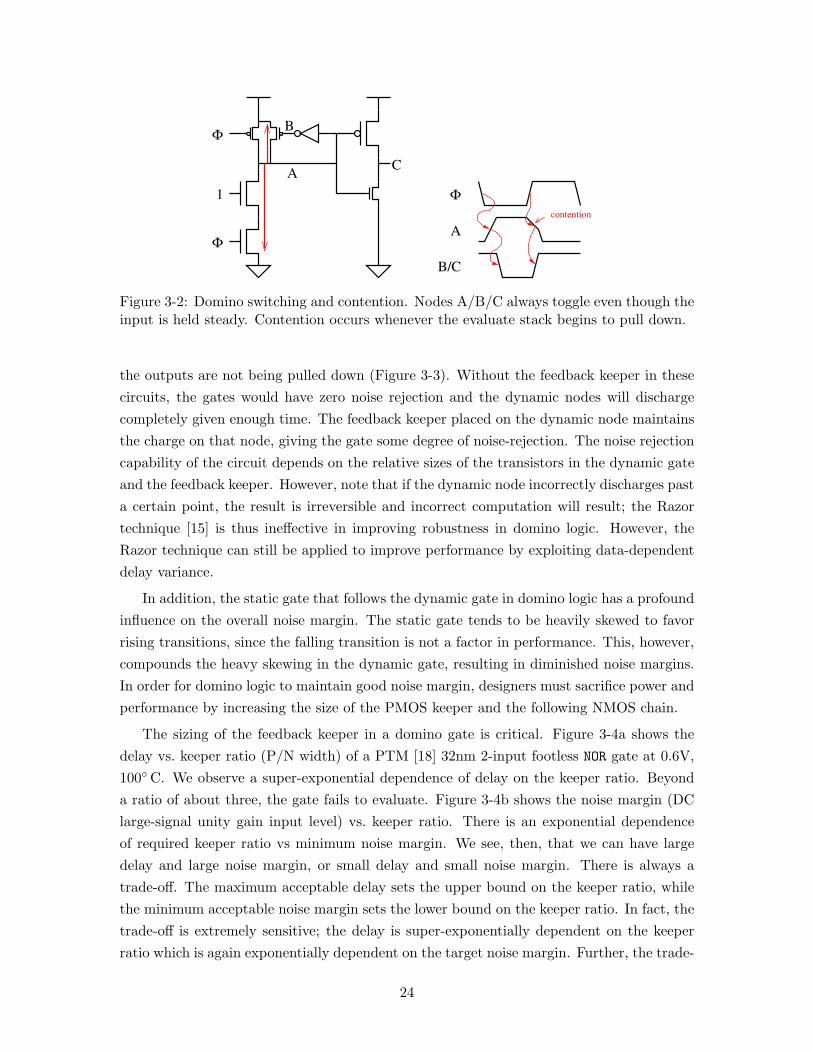
The performance of domino logic comes at the cost of power, robustness, and designeffort. Domino logic burns more power because of the increased number of transitions onthe output net. Figure 3-2 shows the operation of the domino buffer when the data inputis always high. Note that nodes A, B, and C switch twice on each cycle, though they areconceptually holding constant values. The nodes in a static CMOS buffer would not beswitching at all. More generally, for uniformly random input data, the nodes driven bya domino buffer will toggle twice as often as the nodes driven by a static CMOS buffer,neglecting glitching activity. Note also that the feedback inverter and node B would not existin the static CMOS version; thus there is extra capacitance being switched. In addition,domino logic presents a much greater clock load than static CMOS, and thus requiresgreater power to drive. Compared to data nodes of the same capacitance, clock nodesaccount for more power dissipation because of clock tree buffering and greater switchingactivity. Further, the feedback keeper also burns power and degrade performance because ofcontention when the dynamic gate switches. This is shown in Figure 3-2. After precharge,the dynamic node is high, meaning that the feedback keeper is on. When both the datainput and the clock go high, the pull-down chain tries to drive the dynamic node low. Thepull-down chain has to fight the keeper until the keeper itself changes state. The amountof contention, and hence delay degradation and power waste, depends on the relative sizesof the transistors in the dynamic gate and the feedback keeper.
Another complication is that some form of latching is required in between the clockstages. This is because the final domino precharge in the stage erases the output rightwhen the domino gates in the next stage begin to evaluate. Without a latch, the NMOSchain will not have enough time to fully pull down. The latch (or half-latch) captures thedata before the falling edge of the clock that triggers preset, giving evaluate time to work.Extra clock phases or non-50% duty cycle clock waveforms can also solve this issue, at thecost of some complexity.
The absence of a static pull-up chain makes a dynamic gate susceptible to input noise,power and ground bounce, leakage, charge-sharing, and SEP during the evaluate phase if
23
Φ
Φ
C
B
1
A
B/C
Φ
A
contention
Figure 3-2: Domino switching and contention. Nodes A/B/C always toggle even though theinput is held steady. Contention occurs whenever the evaluate stack begins to pull down.
the outputs are not being pulled down (Figure 3-3). Without the feedback keeper in thesecircuits, the gates would have zero noise rejection and the dynamic nodes will dischargecompletely given enough time. The feedback keeper placed on the dynamic node maintainsthe charge on that node, giving the gate some degree of noise-rejection. The noise rejectioncapability of the circuit depends on the relative sizes of the transistors in the dynamic gateand the feedback keeper. However, note that if the dynamic node incorrectly discharges pasta certain point, the result is irreversible and incorrect computation will result; the Razortechnique [15] is thus ineffective in improving robustness in domino logic. However, theRazor technique can still be applied to improve performance by exploiting data-dependentdelay variance.
In addition, the static gate that follows the dynamic gate in domino logic has a profoundinfluence on the overall noise margin. The static gate tends to be heavily skewed to favorrising transitions, since the falling transition is not a factor in performance. This, however,compounds the heavy skewing in the dynamic gate, resulting in diminished noise margins.In order for domino logic to maintain good noise margin, designers must sacrifice power andperformance by increasing the size of the PMOS keeper and the following NMOS chain.
The sizing of the feedback keeper in a domino gate is critical. Figure 3-4a shows thedelay vs. keeper ratio (P/N width) of a PTM [18] 32nm 2-input footless NOR gate at 0.6V,100◦C. We observe a super-exponential dependence of delay on the keeper ratio. Beyonda ratio of about three, the gate fails to evaluate. Figure 3-4b shows the noise margin (DClarge-signal unity gain input level) vs. keeper ratio. There is an exponential dependenceof required keeper ratio vs minimum noise margin. We see, then, that we can have largedelay and large noise margin, or small delay and small noise margin. There is always atrade-off. The maximum acceptable delay sets the upper bound on the keeper ratio, whilethe minimum acceptable noise margin sets the lower bound on the keeper ratio. In fact, thetrade-off is extremely sensitive; the delay is super-exponentially dependent on the keeperratio which is again exponentially dependent on the target noise margin. Further, the trade-
24

0
0
1
0
1
1
(a) Leakage currents.
1
0
1
1
(b) Supply noise.
1
1
1
(c) Input noise.
1
1
0
0
1
(d) Charge sharing.
Figure 3-3: Sources of noise in domino logic. SEP not shown.
25

0 0.5 1 1.5 2 2.5 310
1
102
keeper ratio
dela
y (p
s)
l + 2nmnominall − 2nm
(a)
10−2
10−1
100
0
0.1
0.2
0.3
0.4
0.5
keeper ratio
nois
e m
argi
n (V
)
l + 2nmnominall − 2nm
(b)
Figure 3-4: Keeper sizing for a PTM 32nm 2-input footless dynamic NOR gate at 0.6V,100◦C. Channel lengths are varied by ±2 nm. (a) Delay vs. keeper ratio. One input varyingwith 25ps input rise time. Second input constant 0. 740nm evaluation width. 20fF load.(b) Noise margin vs. keeper ratio. Both inputs varying.
off between performance and noise margin gets worse with scaling. The acceptable rangeof keeper ratios shrinks as technology scales [19].
To make matters worse, domino logic is sensitive to variation. Figure 3-4 also shows thekeeper sizing curves when the transistor channel lengths are varied by ±2 nm, correspondingto approximately 3σ process deviation [2]. Correct operation requires delay to be verifiedat the slow corner and noise margin to be verified at the fast corner. This further shrinksthe range of acceptable keeper ratios. As relative device variability increases, this effect willbecome larger.
Footless domino pipelines require separate delayed clocks for each stage of logic, eachseparated by two slow inverters. The timing constraints for the clocks are complex. Therising edge of each stage’s clock should precede the rising edge of data for performance. Thefalling edge of each stage’s clock should follow the falling edge of data to prevent contention.This careful clock shaping is also sensitive to variation. The clock generation requiresextra area and power and, because of their complexity, are appropriate only in criticaldatapaths and in wide-or structures such as register files where the clock delay circuitry canbe amortized across many gates in a stage. These schemes also require careful analysis. Onemust account for process and environment variation to ensure accurate tracking of clockand data delays.
Because of the keeper sizing issue, the delay/robustness trade-off, and variability con-cerns, it is not clear how well dynamic circuits will scale into the nanometer regime. Astudy of technology scaling on CMOS Logic styles was performed by Anis et al. [20]. Theyshowed that, for the technology nodes from 0.80µm to 0.25 µm, the performance advantageof domino logic over static logic is reduced. Another analytical study by Anders [19] showed
26

that if we hold noise margins to a constant fraction of the supply voltage, the performanceof dynamic circuits are severely degraded at the 70 nm node, and conventional dynamiccircuits cease to function below 70 nm. This last prediction, however, was flawed becauseit presumed voltage scaling would continue. Nevertheless, domino circuits will continue toface serious noise and scaling issues.
In addition to power-performance-robustness scaling issues, domino logic requires ad-ditional design effort because of complex intra-cell routing and routing to reduce noise.Finally, domino logic can only implement non-inverting logic functions, which limits it use.Variations on domino logic such as dual-rail domino, or use of deracers or complementarysignal generators [21], enable inverting logic, but at the cost of increased power and area.
3.3 Conclusion
Static CMOS logic and Domino logic occupy very different points in the energy-delay-robustness space. Static CMOS is good in terms of energy and robustness, but is poorin terms of delay. Domino is good in terms of delay, but is poor in terms of energy androbustness. In particular, it cannot take advantage of the Razor technique for robustnessagainst transient noise. Finally, domino has serious scaling issues. In the following chapters,we show how PSSL combines the best features of static CMOS and domino.
27

28

Chapter 4
Preset Skewed Static Logic
In this chapter, we present Preset Skewed Static Logic (PSSL). PSSL combines the energy-efficiency and robustness of static CMOS logic with the performance of domino logic. Wefirst show how Skewed Static Logic can improve performance in the presence of timing slack.We then show how to generate slack through preset. We then show the implementation ofPSSL logic and PSSL pipelines. Finally we discuss various scaling issues with respect toPSSL.
4.1 Skewed Static Logic
Figure 4-1a shows a chain of four static CMOS inverters. The dashed curve indicates thetransistor activation path, that is, the sequence of transistor chains that are turned on, for arising input transition. The solid curve indicates the transistor activation path for a fallinginput transition. Note that the total path delay times of a rising input and that of a fallinginput are not necessarily the same. There is a trade-off between the two delay times and alsobetween delay and energy; this is controlled by varying the sizes of individual transistors.For example, by increasing the size of transistors under the dashed curve, one can speed upthe response of the circuit to a rising input transition. This comes at the cost of a slowerresponse to falling input transitions and increased energy dissipation. Figure 4-1b showsthis trade-off. The plot shows the energy and delay of two inverters within a long fan-out-of-4 (FO4) chain. The X and Y axes represent delays through rising input and falling inputpaths. The shade at each x,y location indicates the required energy dissipation to achievethe delays. Note that the shade axis is logarithmic.
More generally, consider any multiple-input, multiple-output acyclic combinational cir-cuit. There can be many activation paths. If there is any difference in the delay timesbetween different paths, then there is slack. By appropriately resizing transistors, one canoften use slack to either increase performance or reduce power dissipation.
29

(a)
0 100 200 300 400 500 600 7000
100
200
300
400
500
600
700
delayr (ps)
dela
yf (p
s)
log e
nerg
y (
J)
−12.6
−12.4
−12.2
−12
−11.8
−11.6
−11.4
(b)
Figure 4-1: (a) Inverter Chain (b) Energy-Delay. TSMC 0.18 µm process. FO4 configura-tion. 10.4fF wire load.
Φ
A BC
Φ
A
B
C
Figure 4-2: Preset Skewed Static Logic. Smaller transistors are less critical.
4.2 Preset
A simple PSSL circuit is shown in Figure 4-2. This resembles the chain of static inverters inFigure 4-1a, except that the first inverter has been replaced by a NAND gate with one inputtied to the clock. The logical function of this circuit is the same as the inverter chain.
Let us assume that the input A is expected to arrive at the rising edge of the clock.The operation of this circuit as is follows. First, the falling edge of the clock initiates theprocess of preset. In preset, all circuit nodes are indirectly forced to pre-determined values.In particular, node B rises in turn causing node C to fall, thus completing the preset process.The idea behind the preset process is that we are speculatively computing all the nodes ofthe circuit presuming low input values. This begins one clock phase before the actual inputvalue(s) arrive, so this computation has an extra clock phase to complete.
The rising edge of the clock initiates the process of evaluate. Note that the processof evaluate is independent of the process of preset, and, in particular, evaluate can beginbefore preset completes. If the value of the input node, A is low at the rising edge of the
30

A
B
A B
Φ
Φ
out
Figure 4-3: A 2-input NOR embedded in PSSL preset-high circuitry.
clock and remains low, nothing further happens in the circuit and evaluate is complete.However, if the input node, A, is high when the clock rises or node A rises while the clock ishigh, then it causes node B to fall, in turn causing node C to rise, completing the evaluateprocess.
Whether node A is high or low, eventually node C gets the correct value. However, wehave decoupled the computation for low values of A (the preset process) from the computa-tion for high values of A (the evaluate process), giving the former computation extra timeand thus creating slack in the path of transistors in the preset process (i.e. the preset path).We can take advantage of this slack by reducing the size of transistors in the preset pathto reduce power consumption, or by increasing the size of transistors in the evaluate pathto reduce delay. Preset allows PSSL to outperform generic static CMOS logic. However,preset comes at the cost of extra power consumption because of spurious transitions frominput mis-speculation and extra clocking overhead.
A NAND gate was used to preset nodes high. A similar analysis holds if we use a NOR
gate for preset. This time, preset is initiated by the rising edge of the clock, and node B ofFigure 4-2 is preset low.
One can embed logic into the gate used for preset. Figure 4-3 is an example of a 2-inputNOR gate folded into a preset-high gate. For logic embedding, it is usually preferable to usepreset-high since only a single NMOS transistor is added to the NMOS chain of logic gate.For preset-low, a PMOS transistor is added to the PMOS chain of the logic gate. The latterhas a larger energy-delay impact.
4.3 Unateness
Speedup from preset depends upon the decoupling of the computation for high and lowinputs. This requires that the preset and evaluate paths go through distinct sets of transis-
31

?
??
Figure 4-4: Non-unate logic. Since the bottom input of the XOR gate cannot be knowna priori, a rising input at the top input produces an unknown transition at the XOR gateoutput, producing unknown transitions for all downstream logic.
tors. If the paths coincide at a transistor, the worst case timing path will apply, reducingthe benefits of preset. The paths are distinct only if the boolean logic function being imple-mented is unate, meaning that any particular input transition in any particular directioncan only cause the output to transition in one direction. In others, it is always invertingor non-inverting. Figure 4-4 shows a non-unate logic network, consisting of an XOR gateand an inverter. Since the bottom input of the XOR gate cannot be known a priori, a risinginput at the top input produces an unknown transition at the XOR gate output, producingunknown transitions for all downstream logic.
Even if a function as a whole is not unate, it may be composed of unate subfunctions.These subfunctions can benefit from preset. Performance can be maximized by locatingnon-unate blocks as far downstream from preset circuitry as possible.
4.4 Pipelining
We now examine how to create pipelines using PSSL. We present PSSL using the threemajor clocking schemes: level-sensitive, edge-triggered, and pulsed.
4.4.1 Level-sensitive
Level-sensitive clocking uses alternating transparent latches as timing elements. A two-phase Level-Sensitive PSSL (LS-PSSL) pipeline, shown in Figure 4-5, is the compositionof PSSL pipeline stages of alternating phase, separated by transparent latches. One stagebegins preset when adjacent stages begin evaluate. In LS-PSSL, the transparent latchesserve two purposes. First, they hold pipeline state. Every legal (non-wave pipelined [22])pipeline must have at least one latch in each full pipeline stage. Second, the latches preventthe preset wave-front from propagating to the following stage until after the preset phase.Otherwise, if the wave-front propagates early, it will cause inter-symbol interference as itbecomes indistinguishable from the evaluate wave-front from the previous cycle. However,in contrast to their use in static CMOS pipelines, transparent latches are not used for
32

Φ Φ
A
Φ
BC D E
Φ
A
B
C
D
E
tΦ l
tΦh
2t
t1
Figure 4-5: Two stage Level-Sensitive PSSL pipeline and timing diagram. Only half of thepipeline is shown. Smaller transistors are less critical. 50% duty cycle clocks are assumed.
synchronization (i.e. delay). Every legal pipeline must have a total of exactly one cycle ofdelay in each full pipeline stage. In LS-PSSL, the synchronization is performed by the NANDgates.
The operation of LS-PSSL, shown in Figure 4-5, is as follows. The falling edge of theclock begins preset, causing C to rise, D to fall, and finally E to rise. This path, whose delayis t1, must complete in one clock cycle, less setup delay. This coincides with the closing ofthe second latch at the falling edge of the clock. Therefore we derive the constraint
t1 + ts < tΦh + tΦl (4.1)
where ts is the setup time of the latch.
The rising edge of the clock begins evaluate. The value of A is effectively sampled bythe first latch and NAND gate combination at the rising edge of the clock. If it is low, thenC falls, D rises, and, finally, E falls. This path, whose delay is t2, must complete one setupdelay before the closing edge of the latch. Therefore we derive the constraint
t2 + ts < tΦh (4.2)
Similarly, the equations of the other half of the pipeline (not shown) are given by
t3 + ts < tΦl + tΦh (4.3)
t4 + ts < tΦl (4.4)
The preset path delays, t1 and t3 can be twice as long as the evaluate path delays, t2 andt4.
33

Φ1
Φ0
E
B
C
I
F
G
A
tΦ l
tΦh
2t 4t
time borrowing
time borrowing
Figure 4-6: Two stage Level-Sensitive PSSL pipeline timing with overlapping clocks.
Note that there is a hard edge on every constraint. Each timing path begins at a clockedge and ends at a clock edge. This means that clock uncertainty, or jitter, needs to beconsidered in maximum delay timing analysis. Even worse, for t2 and t4, the jitter needsto be subtracted from each phase, not just each cycle. However, if we allow the clockwaveforms to have greater than 50% duty cycle so that the clocks overlap, then limitedtime borrowing is allowed as data can flow through the NAND gate before the precedinglatch closes[23] (Figure 4-6). Therefore, in this case, jitter does not need to be taken intoaccount for maximum delay analysis. The equations 4.2 and 4.4 are thus replaced by
t2 + t4 < tΦh + tΦl (4.5)
A problem with using overlapping clocks is that the latches no longer prevent the presetwave-front from advancing early. Therefore, all preset paths must meet a minimum pathdelay in order to guarantee correct operation, as if the circuit were wave pipelined. Theseconstraints are given by
tΦl < t1 (4.6)
tΦh < t3 (4.7)
We can also resolve this by using Φn for the latch clock instead of Φn−1. This allows timeborrowing on the evaluate path, but not time borrowing on the preset path.
34

Latch and preset implementation
Table 4.1 shows eight implementations of the latch and preset gate for level-sensitive PSSL.Row (a) is an implementation of Figure 4-5. Since the latches are used in PSSL mainly toprevent the preset from interfering with the evaluation of data from the previous cycle, thelatches can be simplified under certain conditions. These simplified variants are shown inrows (b) through (h).
The variants differ in their properties. This is shown in Table 4.1. The preset/prechargeinput constraints column indicates the required logic level (on preset) of any input signalsthat are preset or precharged. The functional constraint column lists which input edges(rising or falling) must arrive prior to the rising edge of the clock, Φn, to guarantee thecorrect functionality of the circuit. The timing constraint column lists which input edges(rising or falling) must arrive prior to the rising edge of the clock for there to be any benefitfrom preset. The functionality of the circuit is not otherwise affected by not meetingthis constraint. The time borrow column lists which input edge, if any, can benefit fromtime borrowing. Note, though, that a timing constraint on the same edge precludes timeborrowing for all practical purposes. Finally the output preset column indicates the logiclevel to which the output is preset.
The variants shown in rows (g) and (h) combine the latch and preset gate into onedynamic gate. They are equivalent to the variants in rows (d) and (e), except for outputinversion. The dynamic gate variants have lower energy and delay and so are usuallypreferable. Even though PSSL can use dynamic gates, as domino does, they are usedfor completely different purposes. In domino, the dynamic gates are used for their highperformance. In PSSL, the dynamic gates are used to preset downstream logic. Preset isthe source of speedup. Even if the PSSL dynamic gate were slower than its static equivalent,PSSL would outperform static CMOS.
The simplified versions allow time borrowing because of the partial removal of latching.An example pipeline and timing diagram are shown in Figure 4-7.
If the preset/precharge constraints are violated, the state node is not protected fromcorruption by preset. However, the circuit can still operate correctly if the preset paths aresufficiently slow as to not interfere with the evaluation of the previous cycle. This is a formof wave pipelining [22]. Formally, this means that one or both of the following minimumpath delay constraints must be met.
tΦl < t1 (4.8)
tΦh < t3 (4.9)
A reasonable design, however, should ensure that these minimum path delay constraintsapply to only one clock phase so that the clock can be stopped on the other clock phase forstandby operation.
35

input constraints time outputcircuit preset/precharge functional timing borrow preset
a
Φn
Φn−1
Φn−1
rise/fall high
bΦn−1
Φn−1 Φ
n
rise/fall low
c
Φn
Φn−1
low fall rise rise high
d
Φn
Φn−1
low fall rise low
eΦn−1
Φn
high rise fall high
f
Φn
Φn−1
high rise fall fall low
g
Φ
low fall rise high
h
Φ
high rise fall low
Table 4.1: LS-PSSL Preset latches and their properties.
36

Φ Φ Φ
A B C DE
F G H I
Φ
A
B
E
F
I
tΦh
tlΦ
2t
t3
1t 4
t
Figure 4-7: LS-PSSL time borrowing. Full pipeline shown. Smaller transistors are lesscritical.
One complication arises in connecting the output of 2-phase non-overlapping footeddomino logic to the input of LS-PSSL. The domino output can be a narrow pulse aroundthe rising edge of the capturing clock. The dynamic preset gates may not work correctlysince they begin sampling after the rising edge. The best solution is to use one of thelatch/NAND combinations, with Φn for the latch clock.
N-phase clocking
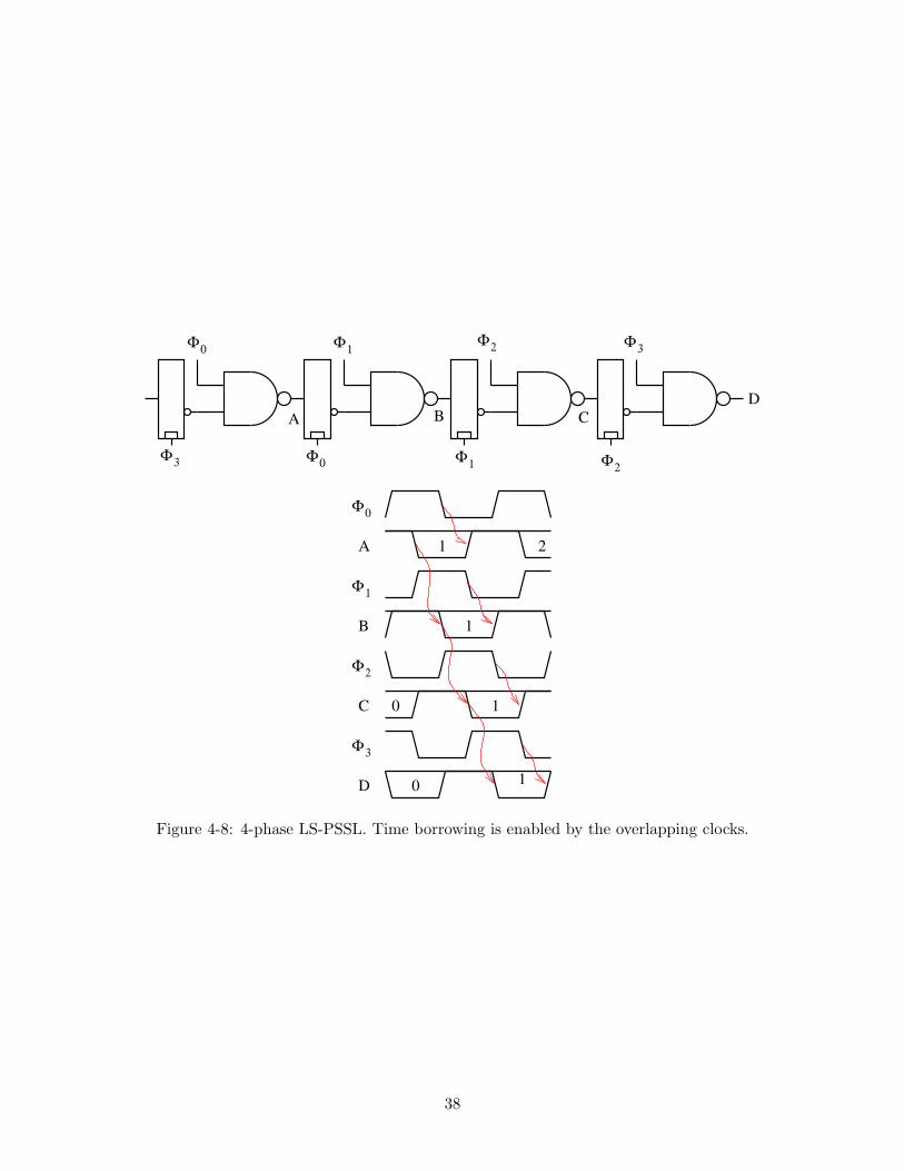
It is possible to extend LS-PSSL to arbitrary numbers of clock phases, as in Figure 4-8.As with a 2-phase LS-PSSL pipeline, each preset path is allowed one cycle to complete.The evaluate paths are allowed, on average, 1/n of a clock cycle. This means a factor of n
speedup on the preset paths. N-phase LS-PSSL, where n > 2, differs from two-phase in thattime borrowing is allowed on the evaluate paths even when the full latch (see Table 4.1a)is used with 50% duty-cycle clocks[23] since the clocks will always overlap. There is alsono preset minimum path delay problem as would occur with a 2-phase overlapping clockdesign since the rising edge of one clock follows the falling edge (from the previous cycle)of the following clock.
The analysis is different when using dynamic gates for the combined latch and preset(see Table 4.1g and h) since there is no separate clock for latching and preset. Figure 4-9
37
Φ0
Φ1
Φ2
Φ3
Φ2
Φ1
Φ0
Φ3
D
CBA
Φ0
Φ1
Φ2
Φ3
0
0
1
1
1
1
A
B
C
D
2
Figure 4-8: 4-phase LS-PSSL. Time borrowing is enabled by the overlapping clocks.
38

Φn
Φn+1
B C D
E
FA
(a)
Φ0
Φ1
Φ2
Φ3
(b)
Φ0
Φ1
Φ2
Φ3
(c)
Figure 4-9: N-phase LS-PSSL using dynamic preset and clock waveforms. (a) Partialpipeline shown. Smaller transistors are less critical. (b) 4-phase 50% duty cycle clock inputwaveforms. (c) 4-phase 25% duty cycle clock input waveforms. Preset path timing is shownin red.
39

Φ Φ
AΦ
BC D E
Φ
A
B
C
D
E
tlΦ
tΦh
t1
2t
Figure 4-10: Edge Triggered PSSL and timing diagram. Full pipeline shown. Smallertransistors are less critical.
shows the pipeline using dynamic preset, along with two timing diagrams with differentclock waveforms. As in the two-phase case, the preset path begins at the falling edge ofthe clock and ends with the rising edge of the clock to the next stage. Using 4-phase 50%duty cycle clocks, the preset paths can take 3/4 of a clock cycle, for a speedup of 3 on thepreset paths. Using 4-phase 25% duty cycle clocks, the preset paths can take one wholeclock cycle, for a speedup of 4. In general, n-phase 50% duty cycle clocks achieve 1 + n
2
speedup whereas 1/n duty cycle clocks achieve n speedup.
4.4.2 Edge-triggered
As opposed to level-sensitive clocking, edge-triggered clocking uses a single monolithic tim-ing element (usually a flip-flop). Figure 4-10 shows a pipeline using the same latch andNAND gate combination as before. However, this time there is only one set in a full pipelinestage, along with the diagram diagram. The corresponding timing constraints are
t1 + ts < tΦh + 2tΦl (4.10)
t2 + ts < tΦh + tΦl (4.11)
t1 > tΦl (4.12)
The timing paths being and end on clock edges so that there is no time borrowingallowed. Note that there is a minimum path delay constraint on clock phase 2. Violatingthis constraint would cause inter-symbol interference. This is a fundamental race conditionthat cannot be avoided. It is impossible to have a data valid window greater than a clockcycle. The constraint means that the clock can only be stopped on clock phase 1 (clockhigh). With a 50% duty cycle clock, a speedup of a factor of 1.5 can be achieved for the
40

C D
π
Φ
π
A
Φ
B E
π
A
B
C
D
E
Φ
tlΦ
tΦh
2t
t1
twπt
dπ
πΦ
Figure 4-11: Pulsed PSSL pipeline with timing diagram. Full pipeline shown. Smallertransistors are less critical.
preset path. If the clock is a narrow pulse, a theoretical speedup of a factor of 2 can beachieved. However, finite rise/fall times and the requirements of latching impose a lowerlimit on the clock pulse width.
4.4.3 Pulsed
Pulsed clocking uses transparent latches that are clocked with narrow pulses. Figure 4-11 shows a pulsed PSSL pipeline along with its timing diagram. It uses a novel flip-flopstructure which we call the Double Pulsed Set Conditional-Reset Flip Flop (DPSCRFF) [24].In the DPSCRFF, the path from input to output is only a single stage of logic. This is thekey to the design’s high-performance. Another advantage is that the data input sees onlya single transistor load which reduces required input drive and energy consumption. Thepulse, π should be timed to follow the rising edge of the clock, Φ. As with the edge-triggeredPSSL, there is an unavoidable race condition, the preset path must take longer than a clockphase. The timing constraints in the general case are given by
tΦl + tdπ + twπ < t1 (4.13)
t1 < tΦh + 2tΦl + tdπ (4.14)
tdπ + twπ < t2 (4.15)
t2 + ts < tΦh + tΦl + tdπ (4.16)
tdπ + twπ is the hold time of the pulsed-latch. No time borrowing is allowed in the generalcase.
41

If the intervening logic is strictly inverting, then the timing constraints are given by
tΦl + tdπ < t1 (4.17)
t1 < tΦh + 2tΦl + tdπ (4.18)
tdπ + twπ < t2 (4.19)
t2 + ts < tΦh + tΦl + tdπ + twπ (4.20)
Limited time borrowing is allowed in the evaluate path if it completes in the middle of thelatching clock pulse.
If the intervening logic is strictly non-inverting, then the timing constraints are givenby
tΦl + tdπ + twπ < t1 (4.21)
t1 < tΦh + 2tΦl + tdπ + twπ (4.22)
tdπ < t2 (4.23)
t2 + ts < tΦh + tΦl + tdπ (4.24)
Limited time borrowing is allowed in the preset path if it completes in the middle of thelatching clock pulse.
In this pipeline, all the state is held in the DPSCRFF outputs. Since these are erasedwhen the clock is low, the clock can only be stopped when the clock is high. Fortunately,there is no minimum path delay constraint on phase 1. One of the potential problems withpulsed clocking is the minimum path delay constraint on phase 2. However, this can usuallybe resolved without slowing down critical paths.
With a 50% duty cycle clock, a speedup of a factor of roughly 1.5 can be achieved forthe preset path. A theoretical speedup of a factor of 2 can be achieved if the pulse is madeinfinitely small and is moved to the right before the falling edge of the clock. However, finiterise/fall times and the requirements of latching impose a lower limit on the pulse width.In addition, the output of the DPSCRFF becomes a narrow pulse, so there is the concernthat the data pulse might actually dissipate before reaching the next stage. Fortunately,the skewing of the logic works to stretch out the pulse. However, the pulse integrity wouldstill need to be verified across process corners.
Pulsed-PSSL and edge-triggered PSSL have similar timing properties. Assuming thatclock pulse generation is not a problem, it is clear that pulsed-PSSL is superior to edge-triggered-PSSL because of the lower device count and latency of pulsed-PSSL. Thereforewe do not consider edge-triggered PSSL in the evaluations.
42

Figure 4-12: Gate leakage, indicated by arrows, in the preset state is predominantly throughthe smaller preset path transistors.
4.5 Leakage and leakage variability impact
Insofar as PSSL pipelines use static gates, PSSL is robust to leakage’s impact on noise mar-gin, even accounting for variability, because static gates have ample noise margin. However,because PSSL static gates will be moderately skewed, the gates will not have the same noisemargin as those in a pure static CMOS pipeline. Leakage, however, does increase the amountof energy consumed in the same way as in static CMOS. We do note, however, that transis-tors in a PSSL pipeline, especially those in the preset path, will be smaller than transistorsin static CMOS pipeline of the same performance. In addition, a node in a PSSL pipelineis statistically more likely to be in the preset state than the equivalent node in the staticCMOS pipeline. In the preset state, gate leakage occurs predominantly from the transistorson the preset path (Figure 4-12). We thus expect a significant decrease in gate leakagebecause of the reduced transistor sizes.
Dynamic gates in PSSL pipelines face the same challenges as those in domino. However,the scale of the problems in terms of design and verification is smaller because there arefar fewer dynamic gates being used. Also, the dynamic gates in PSSL will have highernoise margin than those in footed domino because the static gates following the dynamicgates will not be as highly skewed in PSSL as in domino. This is because the gates in theprecharge path do not contribute to timing, except in extreme cases. This, however, doesnot apply to footless domino styles as the timing of the precharge paths matter. However,footless domino styles have their own issues as described in Section 3.2.
4.6 Variability impact
Variability is a serious concern for pulsed latches as it becomes difficult to predict andcontrol the final shape of the clock pulses. Clock pulses cannot be allowed to dissipate orfail to swing fully. In order to ensure this in the face of variability, the clock buffer treemust be designed to widen the clock pulse as a safety margin as it passes through. This,of course, creates serious hold time issues. Therefore, it is not clear if pulsed-PSSL will beviable in scaled technologies.
43

Pulsed-PSSL, Edge-triggered PSSL, and LS-PSSL (in certain cases) make use of wavepipelining. This technique, however, becomes harder to use in the face of variability. Care-ful analysis of minimum clock width constraints must be performed taking into accountvariability on timing paths. This only becomes a problem if there is no clock frequency thatsimultaneously satisfies minimum clock width constraints on the fast corners and maximumclock width constraints on the slow corners.
4.7 Single Event Phenomena
PSSL shares static CMOS’s ability to recover from SEP. Even the use of dynamic gates inPSSL does not increase the probability of soft error because the dynamic gate replaces whatwould otherwise be a latch. SEP, however, can cause transients that are later captured bystate elements. As described in Section 2.2, the Razor technique can be applied to reduce oreven eliminate the impact of SEP as well as other sources of uncertainty such as variabilityand noise.
4.8 Conclusion
PSSL is an ideal technology to cope with scaling issues. It is more robust than dominobecause of its reduced reliance on dynamic logic. As previously discussed, it becomesharder to use dynamic logic as technology scales because of increased noise and decreasednoise-immunity. PSSL uses dynamic logic gates, not for its lower logical effort, but for itspreset, which can be used to speed up all the downstream logic. Therefore, the reducedperformance of dynamic logic due to scaling becomes unimportant.
44

Chapter 5
Previous Work and Comparison
In this chapter, we describe work that is related to PSSL. We describe in particular severalDomino modifications and Domino-Static hybrids, along with two recently proposed exoticlogic styles. We show that LS-PSSL is higher-performing, easier to design with, more robust,and more widely applicable than existing styles. We also describe work to improve dynamiccircuit robustness to variability. Finally we discuss some work on pipelining and timingelements.
5.1 Logic styles
Conditional Keeper technique
Some variants to dynamic logic have been proposed to enable it to scale better in termsof performance [25, 26, 27, 28]. These techniques modify the feedback keeper to reducecontention. In particular, the conditional keeper technique [26], shown in Figure 5-1, hasbeen successfully used by Intel across three process generations, from 130nm down to 65nm.Here the conventional keeper is replaced with a pair of keepers, a weak fixed keeper and astronger conditional keeper. The conditional keeper only turns on some time after evaluatebegins, giving a small window after the end of precharge for the gate to conditionally pulldown. There is a problem, though, if the input data arrives in the middle of evaluate, as willhappen with gates located at the end of a phase. This is resolved by generating separatedelayed clocks for each stage of logic. Thus this scheme complements footless domino andshares all its design issues, and thus will likely only be used in wide-OR structures such asRAMS and register files.
Noise Tolerant Precharge
Another idea, originally called Noise Tolerant Precharge (NTP), removes the feedbackkeeper entirely and replaces it with a weak static CMOS pull-up [29, 30], as shown inFigure 5-2. However, a more recent study [31], showed that conventional domino was su-
45

Figure 5-1: Conditional-keeper technique. The conventional keeper is replaced with a pairof keepers, a weak fixed keeper and a stronger conditional keeper. The conditional keeperonly turns on some time after evaluate begins to allow time for the gate to switch.
Figure 5-2: Noise-tolerant precharge. The feedback keeper is eliminated and replaced witha weak PMOS pull-up network.
46

perior to NTP in terms of overall energy-delay-robustness. At the same time, NTP is nota complete replacement for dynamic logic. Dynamic logic has the ability to synchronize,that is, to prevent inputs from affecting outputs. It also has the ability to hold, that is, tokeep some memory of old values. These two abilities allow a dynamic gate to function asa latch. NTP, on the other hand, can only synchronize; it cannot hold a value. A pipelineusing only alternating NTP and static gates will work through wave pipelining, but only ata minimum clock frequency. In particular, the clock could not be stopped to save power.Therefore, either latches have to be inserted, adding delay and preventing time borrowing,or some gates need to be converted to dynamic gates. NTP complements PSSL. It can beused in place of a static CMOS gate where the inputs are known to be monotonic and thestatic CMOS gate would have poor performance. It can also be used to replace certaininstances of dynamic gates in PSSL where the hold ability is not required.
Skewed CMOS
A static/dynamic hybrid called Skewed CMOS logic was proposed in [32]. This is basicallya generalized NTP domino where where the clocked stages can be placed anywhere in thepipeline and both precharge high and precharge low NTP are used. In addition, those stagesthat are not clocked are skewed to favor the evaluate transition. The resulting circuits aremore noise tolerant than domino. An example pipeline along with its timing diagram isshown in Figures 5-3. The precharge paths are allowed to take 3 times longer than theevaluate paths because there are three clocked stages in each phase.
Our work is very similar and shares the idea of using skewed static gates for improvedperformance and robustness. They are, however, based on different, but complementary,timing principles. Figure 5-4 compares the execution of similar 18-stage pipelines, one inSkewed CMOS and one in LS-PSSL, having the same 3× precharge/preset speedup. InSkewed CMOS, speedup is attained by having multiple sections of dependent logic in thesame phase precharging simultaneously. Precharge must complete in one phase. The overlapor speedup factor is independent of the number of clock phases. The total number of clockedstages is mn where m is the overlap factor and n is the number of phases. In PSSL, speedupis attained by overlapping the preset of logic in adjacent phases. In LS-PSSL, preset mustcomplete in one clock cycle. Here, the overlap factor is identical to the number of clockphases and the total number of clocked stages is m, since there is exactly one clock stageper phase. Therefore, Skewed CMOS requires a factor of 2 greater clock load for similarLS-PSSL pipelines with similar speedup. Edge-triggered and pulsed PSSL have even lessresemblance to skewed CMOS. For the former, preset must complete in three phases, theoverlap factor is 1.5 for a 50% duty cycle clock, and the total number of clocked stages is1. One final issue is that static latches are required between stages because precharge canarrive early
47

Figure 5-3: 18-stage Skewed CMOS pipeline (half are shown) and timing diagram. Theprecharge paths are allowed to take 3 times longer than the evaluate paths because thereare three clocked stages in each phase.
48

evaluatestableprecharge
time
gate
1 2 3 4 5 6 7 8 9 10 11 12 13 14 15 16 17 18
(a) 2-phase Skewed CMOS with 3 clocked stages per phase. Stages 1,4,7,10,13,16 are clocked.
evaluatestablepreset
time
gate
1 2 3 4 5 6 7 8 9 10 11 12 13 14 15 16 17 18
(b) 3-phase LS-PSSL. Stages 1,7,13 are clocked.
Figure 5-4: Skewed CMOS vs. LS-PSSL execution charts. 18-stage design. Both designshave 3× speedup on the precharge/preset paths.
49

Figure 5-5: Output Prediction Logic.
Output Prediction Logic
Other novel logic styles have also been proposed. In Output Prediction Logic (OPL) [33],shown in Figure 5-5, every gate is preset high using a footed dynamic gate. The risingedges of the clocks to each gate are timed to just precede the falling edges of inputs, suchthat the output is at the high-gain trip point when the inputs arrive. They showed a 2-3x improvement in delay over static CMOS in a wide range of circuits with an averageadditional energy cost of about one third. Subsequently, a 64-bit adder was implementedin OPL with a delay of 409ps in 0.18µm dissipating 325pJ per cycle [34] and another64-bit adder was implemented in differential OPL with a delay of about 226ps in 0.13 µmdissipating 29.5pJ per cycle [35]. Further circuits were described in [36, 37]. A difficulty withOPL is the requirement for precise generation of clocks, separated by less than an FO4 delay.Further the best performance is achieved right when the circuit is about to fail. If the risingedge of the clock arrives any earlier, the circuit fails. If the clock arrives any later, the circuitis clock-blocked, slowing it down. Each additional circuit stage compounds this slowing,as opposed to other logic/pipelining styles which at most block once on each phase. Suchprecise control only becomes more difficult in sub-100nm technologies as device variationand noise cause proportionally more delay variance. Also, this technique is applicable onlyto datapaths where the clock generation overhead can be amortized.
Low-Voltage Swing Logic
Another novel logic style, Low-Voltage Swing (LVS) logic [38], utilizes low-voltage differen-tial signaling and sense-amplifiers–ideas borrowed from RAM design. This allows logic tobe built using large diffusion connected networks, resulting in a huge reduction of circuitnodes. This is especially advantageous for Manchester carry chains and very wide muxesor shifters. Combined with reduced voltage swings, the reduction in circuit nodes yieldsa reduction in power dissipation even while outperforming domino logic. LVS was used in
50

Figure 5-6: Low Voltage Swing Logic.
the design of the Pentium 4 processor at 90nm technology, which ran the integer core at7GHz. Designing with LVS takes a lot of design effort and care, especially to eliminate non-common-mode noise and to ensure layout matching. This level of effort is normally reservedfor RAMs and analog designs and required much work on design tools and methodology. Itis worth noting that LVS was abandoned by Intel at the 65nm node in favor of domino [39]because LVS did not scale well enough to justify the design effort.
5.2 Variability
The static gates in PSSL are robust to variation. Variability is primarily a concern forthe dynamic preset circuitry in PSSL. Techniques that improve robustness with regard tovariability for domino circuits also apply to the dynamic preset circuitry.
Variation-Compensating Dynamic circuit
The Variation-Compensating Dynamic circuit technique [40], shown in Figure 5-7, is similarto the contention reduction techniques described previously. The conventional keeper isreplaced with a set of binary-weighted conditional keepers which are digitally programmedto be on or off to customize the overall keeper strength to track process variation. The NANDgates used for turning on and off the keepers require extra area and add extra capacitanceto the output node. The extra capacitance hurts the energy-delay of the circuit. Thistechnique will be very useful in cases where the output node is already heavily loaded, asin the case of a RAM bit line, so that the added overhead is negligible. However, thistechnique is not as useful in the general case.
51

Figure 5-7: Process- Compensating Dynamic circuit technique. The conventional keeper isreplaced with a set of binary-weighted conditional keepers which are digitally programmedto be on or off to customize the overall keeper strength to track process variation.
Figure 5-8: Leakage Current Replica Keeper. An analog current mirror replicates theleakage current of a reference pull-down stack onto the keeper. This allows the keepercurrent to track the actual leakage current.
Leakage Current Replica Keeper
The Leakage Current Replica Keeper [41], shown in Figure 5-8, uses an analog currentmirror to replicate the leakage current of a reference pull-down stack onto the keeper. Thisallows the keeper current to track the actual leakage current with die-to-die process variationand environment variation. There is little penalty with this scheme, but care must be takenwith the analog KPR signal to avoid noise.
Applicability to PSSL
Schemes that improve dynamic gate robustness to variability inevitably incur area, delay,energy, or design overhead. Since PSSL uses few, if any, dynamic gates, it may be preferable
52

to over-size the keeper and pay the delay penalty. The penalty from over-sizing in PSSLshould be smaller than the penalty for Domino, in proportion to the number of gates ineach pipeline stages
5.3 Pipelining
There has been work on improving performance through better pipelining. In standard two-phase footed domino logic, static latches are required between half-pipeline stages becauseof the early arriving precharge. In [23], Harris describes the removal of static latches,allowing certain dynamic gates to function as latches. This eliminates all synchronizationdelay and enables time-borrowing to be used improve performance. However, doing thiswith a 2-phase clocking scheme requires greater than 50% duty cycle clocks, creating clockgeneration complexity and hold time issues. LS-PSSL with the simplified latches allowstime-borrowing even with 50% duty cycle clocks.
In [22] the authors describe wave-pipelining, where several waves of operands are pro-cessed simultaneously in a combinational circuit without being separated by latches. Subse-quently this was applied to domino logic in [42]. We utilize this technique to allow non-unatesignals to be used with the simplified latch/preset circuitry.
5.4 Timing Elements
Flip-flops are critical timing elements in digital circuits and have a large impact on circuitspeed and power consumption. Consequently, extensive research has been performed todevelop fast and low-power flip-flops [43, 44, 45, 46]. Recently, pulsed latch structures haveemerged as the fastest known flip-flop structures [43, 44]. By reducing the transparencyperiod of a latch to a narrow window, the latch can operate as a flip-flop with the additionaladvantage of allowing limited time-borrowing across cycle boundaries to reduce sensitivityto clock skew and jitter. These structures have the disadvantage of large positive hold timeswhich complicates timing verification. The pulse generators can also consume considerableenergy as pulses must be generated locally to avoid pulse distortion. Nonetheless, because oftheir performance advantages, these pulsed latch structures have been used in several com-mercial high-performance microprocessors [47, 48]. The DPSCRFF is simpler and faster,and, as we will see later, faster and lower-power than other known pulsed latches while alsoproviding logic speedup from preset.
5.5 Conclusion
There is not likely to be a single logic style or logic element that is best for every instance inevery design. However, we believe PSSL complements and improves upon previous work on
53

logic styles and timing elements. It achieves higher performance, lower energy, and higherrobustness. It is also more widely applicable and easier to design with.
54

Chapter 6
Managing Leakage
As leakage is a major scaling concern, we present a survey of techniques to deal with leakage,highlighting special considerations for PSSL.
6.1 Leakage
The leakage paths (Figure 2-1) in a static CMOS inverter chain are shown in Figure 6-1.There are various ways to reduce the leakage. A survey of leakage reduction techniques canbe found in [4]. Four major techniques are multiple-threshold circuits, sleep vector, powergating, and body biasing. We will limit our discussion to the first three. The last techniqueis, for the most part, orthogonal to logic style.
6.1.1 Multiple-Vth circuits
To reduce leakage in active circuitry, one important technique is to use two (or more) typesof transistors, each type with different Vth voltages. In the simplest scheme, the low-Vth
transistors are reserved for gates in the critical paths; high-Vth transistors are used every-where else [49]. In theory, this would cut leakage drastically without hurting performanceor dynamic power. However, the problem is that few paths are truly non-critical sinceany timing slack can be traded for reduced dynamic power through transistor sizing and
gate
BTBT
subthreshold1 0 01
Figure 6-1: Static CMOS leakage paths.
55

(a) original (b) improved
Figure 6-2: Leakage-proof domino circuits. CLK and SLEEP are forced high during sleep,which sets all the nodes low.
possibly voltage scaling. Therefore, a holistic optimization strategy that considers supplyvoltage, threshold voltage, and transistor sizing would be more effective [50]. The multiple-Vth technique adds a degree of freedom in circuit design, providing a way to trade-off staticpower vs. dynamic power vs. delay.
This technique can be applied to all the logic styles, with some minor differences. Instatic CMOS circuits, the Vth choice will generally be made per gate. For each gate, everytransistor will have low-Vth or every transistor will have high-Vth. This is because usually alltiming paths through the gate are (relatively) critical or they are all (relatively) non-critical.As an optimization, deeply stacked transistors might be left as low-Vth since they have lowersubthreshold leakage on average. In domino circuits, the transistors in the precharge path,including the static gate pull-down, always have high-Vth because they are not in any timingpaths. In PSSL circuits, it is beneficial to consider the PMOS and NMOS halves separatelysince they often have wildly different timing constraints. Transistors in the preset path willgenerally be less critical than transistors in the evaluate path; therefore, there is generallyless penalty for using high-Vth devices in the preset path. Using high-Vth devices in thepreset path also tends to reduce the skew ratio of gates and thus will enhance noise-margin.
6.1.2 Sleep Vector technique
Sleep vector techniques take advantage of the fact that the amount of leakage in a circuit isdata dependent. On sleep, a fixed input vector is applied to the primary inputs of a block.This input vector is designed to minimize the leakage in the block [51]. One can furtherreduce leakage, at the cost of energy and delay, by introducing internal control points thatset specific nodes on sleep [52]. Sleep vector techniques, on their own, are highly dependenton circuit topology for their effectiveness and can rarely entirely suppress leakage.
There are various sleep vector techniques specifically suited to domino using multiple-
56

VddVddVddVdd
VddVddVddVdd
VddVdd
sleep
sleepb
clk
in node1 node2(=0)
(=0)
(=1)
(=1)
(1->0) (0->1)
Figure 6-3: Leakage-Biased Domino. Sleep transistors are placed off the evaluate path.Leakage currents bias the circuit into a low-leakage state.
Vth devices. These can almost entirely suppress leakage. Figure 6-2a shows Leakage-proofdomino [53]. CLK and SLEEP are forced high during sleep, driving the dynamic and staticoutputs low and cutting off the static pull-up. There is, however, some performance over-head due to the addition of a high-Vth transistor in the critical pull-up chain of the staticgate. An improved technique [54], shown in Figure 6-2b, eliminates the performance over-head of the earlier technique. In Leakage-Biased Domino [55](shown in Figure 6-3), sleeptransistors are placed off the critical evaluate path. Instead, leakage currents bias the circuitinto a low-leakage state.
The above techniques work because of the high-Vth transistors in the precharge circuitryof domino logic which do not hurt performance. Similar techniques can also work for PSSL,though at some dynamic power and performance penalty, if all transistors in the presetpath have high-Vth.
6.1.3 Power Gating
Another class of ideas uses sleep transistors to cut off power and/or ground from the logic.The original idea of power gating comes from Multithreshold voltage CMOS (MTCMOS)logic [56], shown in Figure 6-4. MTCMOS cuts off the circuit from both rails using high-Vth transistors. MTCMOS was truly ahead of its time. It was proposed not as a way todeal with leakage (which was virtually non-existent in their 0.5 µm technology), but as ahigh-performance low-power circuit technique. Since they used transistors with lower thannormal Vth and used ultra-low supply voltages, they ended up facing the same issues thatdesigners would later face four or five technology generations later. There is also a variantof MTCMOS using only a single sleep transistor.
The problem with MTCMOS is that its high-Vth transistors degrade performance. Incontrast, Super Cut-Off CMOS (SCCMOS) logic [57], shown in Figure 6-5, does not require
57

Vddv
Vssv
X X X X
sleep
sleep
Figure 6-4: Multithreshold voltage CMOS logic. The shaded transistors are high-Vth to cutoff the circuit from both rails.
vVdd
X 0 X 0
sleep
Figure 6-5: Super Cut-Off CMOS logic. The gate of the sleep transistor is boosted aboveVdd in sleep mode to cut off the circuit from the Vdd rail.
high-Vth transistors. Rather, the gate of the sleep transistor is boosted above Vdd in sleepmode to cut off the circuit from the Vdd rail.
A problem with SCCMOS (and single sleep transistor MTCMOS) is the long timerequired to wake up from sleep mode due to the high-capacitance virtual supply node thatneeds to be recharged. During sleep, the virtual supply node is completely dischargeddue to leakage. Zigzag Super Cut-Off CMOS (ZSCCMOS) logic [58], shown in Figure 6-6,addresses this. Low output gates are tied to virtual Vdd and high output gates are tiedto virtual Vss in a zigzag pattern. As in SCCMOS, the gates of the PMOS/NMOS sleeptransistors are boosted above Vdd/below Vss in sleep mode to cut off gates from the Vdd/Vssrails. In this configuration, the virtual rails do not swing as much so their recovery timeis about 11× less than for SCCMOS. A drawback of ZSCCMOS is that gate leakage is notreduced [59].
Gate-leakage Suppressing CMOS (GSCMOS) logic [60], shown in Figure 6-7, is a modi-
58

sleepVddv
sleep
Vssv
1 0 1 0
Figure 6-6: Zigzag Super Cut-Off CMOS logic and leakage paths. Low output gates are tiedto virtual Vdd and high output gates are tied to virtual Vss in a zigzag pattern. The gatesof the PMOS/NMOS sleep transistors are boosted above Vdd/below Vss in sleep mode to cutoff gates from the Vdd/Vss rails. Gate leakage, indicated by the arrows, is not eliminated.
fication of ZSCCMOS to deal with gate leakage. Low output gates are tied to virtual Vdd1and high output gates are tied to virtual Vdd2 and also virtual Vss in a zigzag pattern. Thegates of the PMOS/NMOS sleep transistors are boosted above Vdd/below Vss in sleep modeto cut off gates from the Vdd/Vss rails.
6.1.4 Applications to PSSL
For deep sleep states, where power consumption is the primary concern, the only true wayto eliminate leakage is through power gating. ZSCCMOS is not completely effective andso is not recommended in scaled technologies where gate leakage is large. The MTCMOSand SCCMOS techniques are independent of logic style. For static CMOS logic, usingZSCCMOS and GSCMOS requires applying a sleep vector so that the state of internalnodes is predetermined. Domino and PSSL can use precharge/preset in lieu of a sleepvector.
For fine grained leakage reduction, where low overhead is the primary concern, a sleepvector technique that utilizes high-Vth transistors is best. Domino logic works well withthese schemes because the transistors in the precharge path do not contribute to timing,so it is convenient to put all the high-Vth transistors there. Static CMOS logic, on theother hand, faces a dynamic energy vs. delay vs. static energy tradeoff wherever high-Vth
transistors are used. PSSL, however, opens up new opportunities for managing leakagereduction. Figure 6-8 compares the leakage paths in Static CMOS and multi-Vth PSSL,where all the of transistors on the preset path are high-VthWhen the PSSL circuit is placedin the opposite state of preset, all subthreshold leakage is eliminated, and gate leakage is
59

Vddv1
Vddv2
Vssv
X 0 X 0
sleepsleep
sleep
Figure 6-7: Gate-leakage Suppressing CMOS logic. Low output gates are tied to virtualVdd1 and high output gates are tied to virtual Vdd2 and also virtual Vss in a zigzag pattern.The gates of the PMOS/NMOS sleep transistors are boosted above Vdd/below Vss in sleepmode to cut off gates from the Vdd/Vss rails.
gate
BTBT
subthreshold1 0 01
(a) Static CMOS
gate
BTBT
subthreshold1 0 01
(b) PSSL
Figure 6-8: Comparison of leakage paths in Static CMOS and multi-Vth PSSL. Smallertransistors are on the Preset path and are high-VthWhen the PSSL circuit is placed in theopposite state of preset, all subthreshold leakage is eliminated, and gate leakage is reducedby 1/3. BTBT is also reduced because of the reduced size of the transistors.
60

reduced by 1/3. BTBT is also reduced because of the reduced size of the transistors. Thissame scheme can be applied with Static CMOS logic; however, with PSSL, there is half thedelay penalty (for 2-phase LS-PSSL), since the preset path is stretched over 1 cycle.
6.2 Conclusion
We have surveyed a number of leakage reduction techniques and have found that PSSLcreates opportunities for leakage reduction. We have proposed a fine grained leakage reduc-tion technique that takes advantage of the unique properties of PSSL; this technique hasreduced overhead when used in PSSL as compared to static CMOS.
61

62

Chapter 7
Evaluation
In this chapter we show the effectiveness of PSSL logic quantitatively. Several test circuitswere implemented in PSSL and other logic styles, starting from simple inverter pipelinesand culminating in the implementation of 32-bit accumulators. In addition, the DPSCRFFflip-flop is also compared against existing flip-flop designs.
7.1 Linear Feedback Shift Register
We implemented a 2-bit linear feedback shift register (LFSR) shown in Figure 7-1 usingboth static CMOS logic and LS-PSSL. This LFSR implements the sequence 11,01,00,10(repeated) and was chosen because it is simple and yet exercises the complete set of one-bitstate transitions, providing a good test of pipeline functionality.
7.1.1 Methodology
The design of the LFSR in LS-PSSL is shown in Figure 7-2. Of the four phases, three arenon-inverting, and thus race-free. However, the last phase is inverting and thus presents aminimum path delay with respect to the high phase of the clock. However, as there are nosuch constraints with respect to the low phase of the clock, the clock can be stopped in thatphase. The inverters in the design are skewed such that the preset path delay is roughlytwice the non-preset path delay.
The static CMOS design is similar except that standard latches are used and that,instead of alternately skewed inverters, one type of inverter is used.
D Q
ΦD Q
Φ
Figure 7-1: Two-bit Linear Feedback Shift Register.
63

Φ Φ Φ Φ
P N P P N P P N P P N P N
Figure 7-2: Linear Feedback Shift Register implemented using LS-PSSL. Feedback deviceshave been omitted for clarity. Inverters labeled P/N are skewed to favor the rising/fallingtransition respectively.
These were tested using HSPICE in a TSMC 0.18 µm process with estimated deviceparasitics. All nodes were loaded with 12fF of capacitance to represent the loading of wireand of other logic. The minimum clock period and the energy dissipation, excluding clockenergy, was measured for each design point.
The static CMOS design was hand optimized to generate the energy-delay curve. Wethen optimized the PSSL design to have minimum delay subject to a 460fJ energy constraint,which is about the median among the static CMOS energies.
7.1.2 Results
The results are shown in Figure 7-3. The PSSL implementation runs at about 1.5GHzwhereas static CMOS implementation runs at about 1GHz when dissipating about 460fJper clock cycle. This comparison was performed with a fixed load at each node. Theimprovement would be even better if the load scaled with the sizes of the inverters becauseof the lower input capacitance of PSSL.
The simulation waveforms for the last stage of the LFSR is shown in Figure 7-4. Thetop graph shows the output of the dynamic gate. There is an extra pulse whenever theoutput remains in a 0 state. It thus toggles twice as often as the equivalent node in thestatic CMOS implementation. Subsequent graphs show the outputs of successive inverters.The pulse is attenuated and eventually eliminated. This occurs because of the skew in theinverter chain. The faster evaluate path eventually overtakes the slower preset path. Thisreduces the energy penalty of preset so that PSSL can attain better energy-delay. It canbe noted that this effect is timing dependent. The faster the circuit is run, the faster thepreset pulse is eliminated and the less energy per cycle is expended.
7.2 Shift register using wide fan-in gates
We implemented a 4-bit shift register to further compare PSSL to other logic styles. Thedesign of the shift register is shown in Figure 7-5. In contrast to the 2-bit LFSR of theprevious section, the 4-bit design is non-inverting and thus has a straightforward dominoimplementation. Also, instead of inverters, we used alternating 3-input NAND and NOR gates.
64

0 200 400 600 800 1000 1200 14000
100
200
300
400
500
600
minimum clock period (ps)
ener
gy p
er c
ycle
(fJ
)
SCMOSPSSL
Figure 7-3: Linear Feedback Shift Register energy-delay comparison at 0.18µm, 1.8V, TT,25◦C.
Vo
ltag
es (
lin)
0
500m
1
1.5
Vo
ltag
es (
lin)
0
500m
1
1.5
Vo
ltag
es (
lin)
0
500m
1
1.5
Vo
ltag
es (
lin)
0
500m
1
1.5
Vo
ltag
es (
lin)
0
500m
1
1.5
Time (lin) (TIME)0 2n 4n 6n 8n 10n 12n
pssl level-sensitive lfsr
Figure 7-4: LS-PSSL LFSR waveforms. The top graph is the output of the last dynamicgate in the design. Subsequent graphs show the outputs of successive inverters.
65

���������������
���������������
Φ Φ Φ Φ Φ Φ Φ Φ
Φ
Figure 7-5: Four-bit shift register using wide-fan-in gates.
This structure was chosen because it mimics the implementation of very wide fan-in gates.In addition, this structure highlights the advantages of skewed logic styles such as PSSLand domino. It also provides a vehicle for examining the scaling of wide-fanin circuits intonanometer technologies. Domino, footless-domino, static CMOS, and LS-PSSL designs werecompared.
7.2.1 Methodology
We chose to limit our evaluation to designs requiring only 50% duty cycle clocks. ForDomino, this would normally mean the insertion of static latches between pipeline stagesto solve the precharge race condition. This has the drawback of adding two extra stages oflogic in the pipeline. Instead, the last NAND gate of each stage has an extra clock NMOStransistor to form a half-latch (with full keeper). For Footless Domino, this means that thedelays of the precharge and evaluate phases has to match. Higher performance could beattained by relaxing the duty cycle requirement. However, it is not clear how feasible thiswould be in practice. The LS-PSSL version uses dynamic gates for preset to minimize delayand to avoid the penalty of clock jitter.
The static CMOS version uses a fully static 8-transistor inverting latch between stages.This intentionally inverts each half-pipe stage so that the slow path through the gates isfollowed by the fast path. Using time borrowing, the minimum clock period becomes thesum of the delays of the fast and slow paths, instead of twice the slow path as would be thecase without the inversion.
We randomly generated variants of each of the four designs. Each variant was simulatedin Hspice using the PTM [18] 32nm process at 0.6 volts, 100◦C, and with 1fF of capacitiveload at each node in addition to estimated device parasitics. For each design, the delay
66
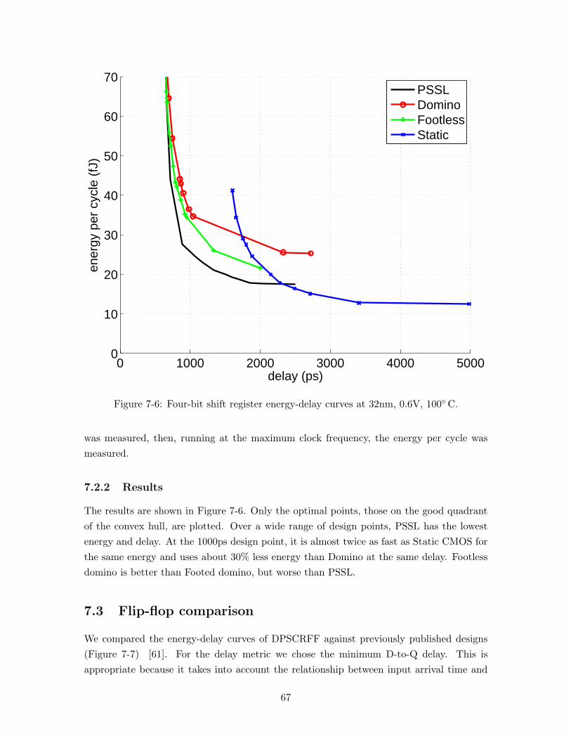
0 1000 2000 3000 4000 50000
10
20
30
40
50
60
70
delay (ps)
ener
gy p
er c
ycle
(fJ
)
PSSLDominoFootlessStatic
Figure 7-6: Four-bit shift register energy-delay curves at 32nm, 0.6V, 100◦C.
was measured, then, running at the maximum clock frequency, the energy per cycle wasmeasured.
7.2.2 Results
The results are shown in Figure 7-6. Only the optimal points, those on the good quadrantof the convex hull, are plotted. Over a wide range of design points, PSSL has the lowestenergy and delay. At the 1000ps design point, it is almost twice as fast as Static CMOS forthe same energy and uses about 30% less energy than Domino at the same delay. Footlessdomino is better than Footed domino, but worse than PSSL.
7.3 Flip-flop comparison
We compared the energy-delay curves of DPSCRFF against previously published designs(Figure 7-7) [61]. For the delay metric we chose the minimum D-to-Q delay. This isappropriate because it takes into account the relationship between input arrival time and
67

Vdd
D
Clk
Q
VddVdd
D
ClkbClkb
ClkbClkbClk
ClkClk
Q
Clk
Vdd
Vdd
D
Clk
Q Qb
Db
Clk
PClk
D
Q
(a) PowerPC 603 master-slave latch (PPCFF)
(b) StrongArm110 flip-flop (SAFF)
(c) SSASPL (d) Hybrid Latch Flip-Flop (HLFF)
Figure 7-7: Flip-flops for comparison
Clk-to-Q delay [45].
7.3.1 Methodology
All flip-flops were simulated using Hspice from schematic netlists annotated with accuratesource/drain parasitic diode parameters using a TSMC 0.25µm process. Figure 7-8 showsthe test-bench used for the evaluation. The test-bench is based on that in [61]. However, wechose more balanced 2/1 inverters instead of minimum sized inverters in the data and clockbuffers. As in [61, 45], we subtracted out the energy dissipated in charging and dischargingthe output load capacitors. In addition, as in [45], we also subtracted out the energydissipated in the input buffers.
The relative ranking of flip-flops depends on the loading conditions assumed [62]. Forthis evaluation, we chose a load of 7.2 fF which corresponds to four minimum sized invertersin this technology. This represents a typical light load in a datapath structure [61]. Todrive higher loads, it is likely that additional levels of output buffering should be used [62].
68

TE
7.2 fFD
CData In
Clock
Q
Figure 7-8: Test-bench setup. Balanced FO4 2/1 inverter trees provide realistic inputwaveforms.
The pulse generators of the DPSCRFF and the SSASPL were connected to four of theflip-flops, and the energy cost of the pulse generation is considered to be amortized betweenthem.
The transistor sizes in the designs were each optimized for several design points. Thisoptimization was performed using data inputs that were stable well before and after thearrival of the clock. The clock was un-gated and the data alternated on every cycle. Clk-to-Q delay and energy were measured. Afterward the minimum D-to-Q delays were foundby optimizing the data input arrival times.
7.3.2 Results
Figure 7-9 show the results. As can be seen, the fastest DPSCRFF at 54 ps is significantlyfaster than the next fastest flops, HLFF and SSASPL, at roughly 150 ps. The lowest-powerDPSCRFF at 141 fJ is comparable to the lowest-power flop, PPCFF, at 130 fJ. However, ithas a propagation delay of only 167 ps compared to 342 ps.
Figure 7-10 show how the energy dissipation varies with different clock and data inputpatterns for the different flip-flops. Note that the flip-flops shown in this figure have widelyvarying propagation delays as shown by the labels in the axes. When the data is heldlow while the clock continues to run, the energy dissipation of the DPSCRFF is reduced.However, if the clock is running and the data is held high, the DPSCRFF actually dissipatesmore power than for the full activity waveforms because of its output glitches. When theclock is held stable, no internal nodes change state and only the single data input gatetoggles. The DPSCRFF therefore has low energy when the local clock is gated.
69

0 50 100 150 200 250 300 350 400 450 5000
50
100
150
200
250
300
350
Delay (ps)
En
erg
y p
er c
ycle
(fJ
)
DPSCRFFHLFFPPCFFSAFFSSASPL
Figure 7-9: Energy versus delay for various flip-flops at 0.25 µm, 2.5V, TT, 25◦C.
DPSCRFF−63ps HLFF−148ps PPCFF−318ps SAFF−378ps SSASPL−148ps0
50
100
150
200
250
300
350
Ene
rgy
per
cycl
e (f
J)
clock lowdata lowdata highfull activity
Figure 7-10: Energy Dissipation across different input waveforms for various flip-flops.
70

reset
+
Figure 7-11: Accumulator design. The datapath is 32-bits wide. The inverter chain addsextra delay to facilitate two-phase clocking.
pg pg pg pg pg pg pg pg pg pg pg pg pg pg pg pg pg pg pg pg pg pg pg pg pg pg pg pg pg pg pg pg
cmcmcmcmcmcmcmcmcmcmcmcmcmcmcmcm
cmcmcmcmcmcmcmcmcmcmcmcmcmcmcmcm
cmcmcmcmcmcmcmcmcmcmcmcmcmcmcmcm
cmcmcmcmcmcmcmcmcmcmcmcmcmcmcmcm
cmcmcmcmcmcmcmcmcmcmcmcmcmcmcmcm
sum
muxmux mux mux mux mux mux mux mux mux mux mux mux mux mux mux
sum sum sum sum sum sum sum sum sum sum sum sum sum sum sum sum
ab31
s32 s0
ab0 c
Figure 7-12: Adder architecture. The hybrid carry-lookahead/carry-select implementationcomputes every other carry bit in the lookahead tree, like a Han-Carlson adder, saving areaand energy, but precomputes the final sum bits to reduce the number of logic stages by one.
7.4 32-bit Accumulator
Adders are an important case to consider as they are found in the critical paths of micro-processors and DSP’s. We implemented a 32-bit accumulator to serve as a realistic test casefor PSSL. The accumulator design is shown in Figure 7-11. Some extra delay was added tothe pipeline to facilitate two phase-clocking.
For the adder we chose a hybrid carry-lookahead/carry-select architecture shown inFigure 7-12. Like in a Han-Carlson adder, the carry-lookahead tree only computes everyother carry bit, so requires only half the resources as a full carry-lookahead. However, unlikethe Han-Carlson which has a final ripple carry calculation to calculate the remaining carrybits, this design precomputes two versions of each 2-bit sum, reducing the number of logicstages by one. Static CMOS, domino, LS-PSSL, and pulsed-PSSL variants were designedand evaluated.
7.4.1 Implementation
A carry-lookahead adder has three major components: carry-generation, partial-sum gen-eration, and final-sum generation. The former two operate in parallel and the results arecombined in the last component. Carry-generation is unate. Partial and final sum gen-
71

eration, however, are not unate. There is, therefore, some amount of trickery involved indesigning a PSSL or domino implementation. One solution for domino implementation isto use a dual-rail scheme throughout. However, this is inefficient as the carry-generationcomponent forms the bulk of the circuitry. Another solution is to employ de-racers or com-plementary signal generators at the boundaries of unate and non-unate sections [21]. Thisis the solution that is chosen in our design. However, some of the de-racers are in the criticalpath between carry-generation and final-sum generation. This is unavoidable in the dominoand pulsed-PSSL designs. However, one of the advantages of LS-PSSL is that non-unatelogic is allowed if certain minimum-path timing restrictions are met. We take advantageof this to remove the de-racers at the output of the carry-generation component. All theversions were designed to be as similar as feasible to one another for fair comparison.
7.4.2 Evaluation
We simulated the designs in the TSMC 0.18 µm micron process at 1.8V and 1.2V. Thenetlist was annotated to include estimated wire and source/drain parasitics. To measurecritical path delay we used Pathmill, which is a transistor level static timing analysis tool.To measure energy consumption we used Nanosim to simulate the accumulator designs over9 cycles with the same set of random input data. The supply energy draw for the entiredesign was measured.
In order to generate energy-delay curves we designed and implemented an algorithmto optimally size transistors in the circuit. The algorithm begins with the circuit in theminimum size/lowest energy configuration. In each iteration it selects the transistors whichcontrol the node in the critical path of the design with the slowest transition time. Risingtransitions are given a
√3 delay factor over falling transitions. The sizes of the selected
transistors are increased so that the transition times on the critical paths will tend tobe more balanced. These ideas were drawn from [17]. The algorithm results comparedfavorably with those from hand optimization.
The results are shown in Figure 7-13. At 1.8V LS-PSSL is superior to static CMOSexcept at the lowest energy points and is superior to domino except at the lowest delaypoints. At the 500ps design point, it uses 20% less energy than domino and is 33% fasterthan static CMOS. At 1.2V the results are qualitatively similar. However, the voltagescaling does not degrade the performance of static CMOS as severely so the crossover pointbetween static CMOS and PSSL occurs at a higher point on the curve.
7.5 Conclusion
We have tested PSSL and compared it against other common logic styles, using several testcircuits from shift registers to accumulators. We have shown that, over a wide range ofdesign points, PSSL is superior to domino and static CMOS logic in terms on energy and
72

0 200 400 600 800 1000 12000
2
4
6
8
10
12
14
16
delay (ns)
ener
gy p
er c
ycle
(pJ
)
PSSLDominoStatic
(a) 1.8V
0 200 400 600 800 1000 1200 1400 1600 18000
0.5
1
1.5
2
2.5
3
3.5
4
4.5
5
delay (ns)
ener
gy p
er c
ycle
(pJ
)
PSSLDominoStatic
(b) 1.2V
Figure 7-13: 32-bit accumulator comparison at 0.18 µm, TT, 25◦C
73

delay, and at the same time is more robust than domino. In particular, we have shown 20-30% energy reduction vs. domino and 33-50% delay reduction vs. static CMOS. In addition,we have presented the Double Pulsed Set Conditional-Reset Flip Flop (DPSCRFF), which istwice as fast as previous flip flops described in literature while consuming the same amountof energy.
74

Chapter 8
Testchip
To demonstrate the advantages of PSSL in real hardware, we built a custom test-chip in theTSMC 180nm process with three ALU cores, using the static CMOS, domino, and LS-PSSLlogic styles. In this chapter, we describe the design, implementation, operation, and testingof this chip. We also present initial energy delay performance comparisons between theALUs implemented in the three logic styles.
8.1 Architecture
A block diagram of the test-chip is shown in Figure 8-1. The ALU cores consume a 40-bitinput vector and produce a 32-bit output word on every cycle, at up to roughly 1 GHz, fora total bandwidth of up to about 72Gb/s. A fourth pass-through ALU merely passes inputsto outputs and can be used for end-to-end testing of the test infrastructure. The testchipreuses an existing socket and bus interface in order to limit the hardware and softwaredesign effort. Data is communicated on/off-chip through the Asynchronous Host InterfaceProtocol (AHIP) bus. This 8-bit bidirectional bus operates in the low tens of megahertzwith a 50% control overhead, for an effective bandwidth of roughly 50-100Mb/s.
8.1.1 Test infrastructure
To verify correct operation of the cores, a mechanism must exist to provide known testvectors and to check results. The simplest and most flexible mechanism feeds input dataand samples output directly from off-chip at full-speed. This is, however, impossible becauseof the 1000× discrepancy between required and available bandwidth, even if we allow fortest compression techniques.
Since the AHIP bus does not have the required bandwidth to supply the ALUs, aninternal 128-entry 40-bit Pattern Generator RAM (PGRAM) is included to provide inputdata to the cores at full speed. The contents of the PGRAM are written offline, throughthe AHIP bus. In addition, a 128-entry 32-bit Logic Analyzer RAM (LARAM) is included
75

static
domino
LS−PSSL
serialize
level−
shift/m
ux
deserialize
AHIP
PGRAM LARAM
4X frequency
passthrough
Figure 8-1: Test-chip block diagram.
to capture output data from the cores at full speed. The contents of the LARAM are readoffline, also through the AHIP bus. The core operating frequency of 1 GHz is well beyondthe capabilities of the test infrastructure, and in particular the RAMS. Therefore, mostof the chip runs at a quarter of the core frequency. Together, the LARAM and PGRAMallow full cycle-level control and visibility of the ALU inputs and outputs. The LARAMcontents can be compared to expected results offline to determine whether a particular ALUfunctioned as expected.
An internal register selects the active ALU. This register can be written to through theAHIP bus. Only the active ALU is clocked. The outputs of the active ALU are writteninto the LARAM.
8.1.2 Measurement infrastructure
The core clock can be provided either by an off-chip clock generator or by an internal voltagecontrolled oscillator. In either case, the frequency can be measured through an external pin.The frequency of the internal clock generator is set by the voltage on an external pin. Thevoltage-frequency relationship of the internal clock generator is shown in Figure 8-2.
Each of the ALUs, except the pass-through ALU, is connected to a separate powersupply. The voltage for each power supply can be digitally set and measured. In addition,
76

0 0.2 0.4 0.6 0.8 1 1.2 1.4 1.610
6
107
108
109
1010
Voltage (V)
Fre
quen
cy (
hz)
Figure 8-2: On-chip VCO frequency vs. input voltage at 1.8V, 25◦C.
the current can be measured and recorded digitally in real time. This allows one to measurethe power consumption of each ALU.
8.1.3 Chip operation
On each slow cycle, the PGRAM produces four input vectors. These are fed serially tothe ALUs on each core cycle. The outputs of the ALUs are level-shifted to the main chipvoltage of 1.8V. On each core cycle, one of the shifted outputs are selected and fed into thedeserializer, which produces a 4-word wide vector on each slow cycle, which is then writteninto the LARAM.
8.1.4 ALU architecture
The architecture of each ALU is shown in Figure 8-3. This architecture is chosen to mimicthe critical ALU bypass path of microprocessors. A pair of input muxes select data fromeither outside the ALU (presumably the register file), the output of the ALU (for the primarypipeline bypass), or from one of two other inputs (representing other possible input sources).The last two inputs are tied to 0 and -1. An XOR in the second input path, along with thecarry input, allows the selectable computation of A+B, A−B, A+B+1, and A−B−1. Anoutput mux selects data from either the output the adder, or from one of three other inputs(representing the outputs of other functional units such as shifters or logic units). Thisorganization is fairly typical. That said, the exactness of correspondence of this datapathto any other ALU datapath is unimportant.
77

+Φ
Φ
Φ
Figure 8-3: ALU block diagram.
8.2 Implementation
The adders in the ALUs are the same as those described in section 7.4, except for transistorsizes.
8.2.1 Transistor size selection
The theory of transistor size selection is as follows. Let S ⊂ <n be the set of valid transistorsize vectors. Let s be a transistor size vector such that s ∈ S. Let V ⊂ < be the set of validsupply voltages. Let v be a supply voltage such that v ∈ V . Let y(s, v) and x(s, v) be theenergy and delay, respectively, of the circuit at the given sizes and voltages. A well chosentransistor size design point is such that the energy-delay trade-off from voltage scaling isidentical to the energy-delay trade-off from transistor sizing. In general, this is describedby a curve in S×V that satisfies ∇y(s, v) = λ∇x(s, v) for λ ∈ <. Second order constraintsalso apply to filter out local maxima and saddle points. Different values of λ yield differentpoints on the optimal curve.
For our purposes, we wish to optimize around the point at v=1.8V. Since we are onlyinterest in that point, we can prune the search space by only considering points at 1.8V.We first trace a curve in S that satisfies ∇y(s, 1.8) = λ∇x(s, 1.8). This was done withthe assistance of a computer program using an algorithm based on gradient descent butmodified to prune the search space by only looking at transistors on the critical path. Wethen retraced the curves at v=1.5V to give an approximation for ∂y
∂v , ∂x∂v at every point.
This algorithm was applied to each of the three ALU designs. The resulting energy-delay curves, based on extracted and back-annotated parasitics, are shown in Figure 8-4.Energy results are from Nanosim spice simulation. Delay results are from Pathmill statictiming analysis. Note that we did not consider noise-margin in the transistor sizing.
The energy-delay efficient point is determined by dy/dsdx/ds = ∂y/∂v
∂x/∂v . Using this equation,we chose the PSSL design point of just under 1GHz frequency. We sized the domino designto be approximately the same speed as the PSSL design at 1.8V. We sized the static CMOS
78
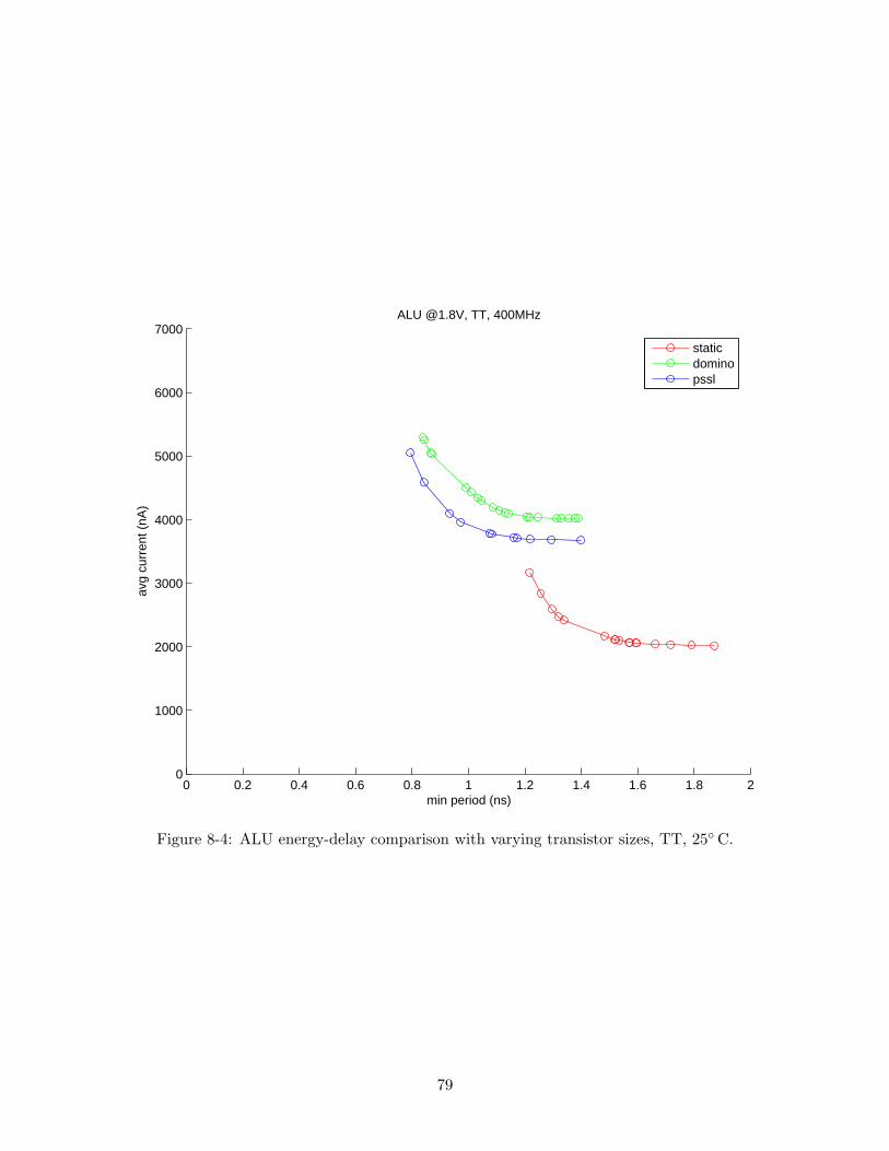
0 0.2 0.4 0.6 0.8 1 1.2 1.4 1.6 1.8 20
1000
2000
3000
4000
5000
6000
7000
min period (ns)
avg
curr
ent (
nA)
ALU @1.8V, TT, 400MHz
staticdominopssl
Figure 8-4: ALU energy-delay comparison with varying transistor sizes, TT, 25◦C.
79

design to consume approximately the same energy as the PSSL design at 1.8V.
It can be argued that this comparison is unfair because the domino ALU should havebeen implemented at a faster design point, then run at a lower voltage for comparisonagainst PSSL. Similar, the static ALU should have been implemented at a slower designpoint, then run at a higher voltage for comparison. However, we felt that this would makethe comparison less clear. Also, it may be unreasonable to increase the voltage of the staticALU beyond 1.8V and risk gate breakdown.
8.2.2 Layout
A die plot of the testchip is shown in Figure 8-5. The chip was built using a semi-customtool-flow. The datapath leaf-cells were drawn manually, but the datapaths were placed androuted procedurally, using custom software written by this author. All datapath leaf cellsand standard cells were designed to a height of 9 wiring tracks, or 5.04 µm. The sizes foreach ALU is shown in table 8.1.
style width (µm) height (µm) area (µm2)Domino 97.68 176.4 17231LS-PSSL 112.2 176.4 19792
Static CMOS 169.62 176.4 29921
Table 8.1: Testchip ALU size comparison.
8.3 Simulation Results
A comparison of the energy and delay of the ALUs in the testchip is shown in Table 8.2.The results are from simulation of fully extracted layout at 1.8V, TT, 25◦C.
8.4 Test and Measurement Methodology
In order to generate an energy-delay curve for each ALU, we need to find the maximumfrequency the ALU can operate at for various supply voltages. This is complicated by thefact that there is no direct control, without additional hardware and software support, over
ALU speed (MHz) energy (pJ/cycle)PSSL 847 23.4Static 687 25.0
Domino 868 27.0
Table 8.2: Testchip ALU Energy-Delay comparison. Simulated with fully extracted layoutat 1.8V, TT, 25◦C.
80

Figure 8-5: Testchip die plot.
81

the clock frequency and measuring the clock frequency is a manual process through theoscilloscope.
Therefore, we break the process into two steps. The first step is to measure the VCOclock frequency vs VCO input voltage. We start at a low input voltage and steadily increasethe voltage by a small increment each time, all the while recording the clock frequencies.
In the second step we try to find the maximum VCO input voltage for each ALU supplyvoltage for which the ALU generates the correct output vectors. The step will be performedcompletely automatically by software. The process is as follows:
1. load the test input vectors2. set the ALU select register3. set the VCO input voltage to the minimum4. set the ALU supply voltage to the minimum5. wait a short time6. read the output vectors7. compare output vectors against expected results8. if the vectors match then
(a) record VCO input voltage, ALU supply voltage, average current draw
(b) increase the VCO input voltage by some small fixed amount
otherwise increase the ALU supply voltage by some small fixed amount.9. repeat from step 5
We finally combine the data from the two steps to yield the final energy delay curve.
8.5 Conclusion
We have designed and submitted for fabrication a testchip demonstrating functional PSSLALUs. Initial simulations indicate that the PSSL ALU has lower energy consumption thanthe equivalent domino logic ALU over some range of delays. We have also shown that ithas higher performance than the equivalent static CMOS ALU over some range of energyconsumption. This testchip is currently in fabrication.
82

Chapter 9
Conclusion
In this work we have introduced and demonstrated Preset Skewed Static Logic (PSSL), anovel high-performance, low-power, robust family of logic styles. Over a wide range of designpoints, PSSL is superior to domino and static CMOS logic in terms on energy and delay,and at the same time is more robust than domino. In particular, we have shown 20-30%energy reduction vs. domino and 33-50% delay reduction vs. static CMOS. In addition, wehave presented the Double Pulsed Set Conditional-Reset Flip Flop (DPSCRFF), which istwice as fast as previous flip flops described in literature while consuming the same amountof energy.
9.1 Summary of Contributions
The main contributions presented in this thesis are:
• PSSL design. We have described the structure and operation of the novel PSSL logicstyle, and shown how to build pipelines using three PSSL clocking schemes: level-sensitive, edge-triggered, and pulsed.
• Leakage reduction techniques. We have proposed a fine grained leakage reductiontechnique that takes advantage of the unique properties of PSSL. This technique hasreduced overhead when used in PSSL as compared to static CMOS.
• PSSL evaluation. We have tested PSSL and compared it against other common logicstyles, using several test circuits from shift registers to accumulators. We have alsodemonstrated the advantages of the DPSCRFF, a novel pulsed latch based flip-flop,for high speed pipelines.
• Testchip. We have implemented a testchip in TSMC 0.18µm technology containing32-bit ALUs using the logic styles PSSL, domino, and static CMOS to demonstratethe feasibility of PSSL. This chip is currently in fabrication.
83

9.2 Future Work
There are several research directions that can be pursued based on this work:
Robustness
The robustness advantage of PSSL over domino can be more fully examined and quantified.Issues such as soft error, transient noise, and variability each present different failure modesand these effects should be fully analyzed.
Leakage Reduction
Further leakage reduction techniques should be explored. The leakage reduction techniqueproposed in this work can form the basis.
Synthesis and Related Tool Flow
Skewed logic styles present challenges to conventional synthesis tool flows. Unique oppor-tunities may exist to improve the quality of synthesis results through novel algorithms andheuristics.
84

Bibliography
[1] Gordon E. Moore. Cramming more components onto integrated circuits. Electronics,38(8), April 1965.
[2] International technology roadmap for semiconductors. http://public.itrs.net.
[3] Deo Singh and Vivek Tiwari. Power challenges in the internet world. In Cool Chips Tu-torial: An Industrial Perspective on Low Power Processor Design, pages 8–15, Novem-ber 1999.
[4] Kaushik Roy, Saibal Mukhopadhyay, and Hamid Mahmoodi-Meimand. Leakage currentmechanisms and leakage reduction techniques in deep-submicrometer CMOS circuits.Proc. IEEE, 91(2):305–327, February 2003.
[5] Saibal Mukhopadhyay, Arijit Raychowdhury, and Kaushik Roy. Accurate estimationof total leakage in nanometer-scale bulk CMOS circuits based on device geometry anddoping profile. IEEE Trans. Computer-Aided Design of Integrated Circuits and Sytems,24(3):363–381, March 2005.
[6] A. Agarwal et al. Leakage power analysis and reduction: models, estimation and tools.IEE Proc. Comput. Digit. Tech., 152(3):353–368, May 2005.
[7] Arjit Raychowdhury, Saibal Mukhopadhyay, and Kaushik Roy. Modeling and estima-tion of leakage in sub-90nm devices. In Int. Conf. VLSI Design, pages 65–70, 2004.
[8] Gordon Moore. No exponential is forever: but ”forever” can be delayed! In ISSCC,pages 20–23, February 2003.
[9] Ofri Wechsler. Inside Intel Core microarchitecture. ftp://download.intel.com/technology/architecture/new architecture 06.pdf.
[10] Samuel K. H. Fung et al. 65nm CMOS high speed, general purpose and low powertransistor technology for high volume foundry application. In Symp. VLSI Tech., pages92–93, 2004.
[11] Saibal Mukhopadhyay and Kaushik Roy. Modeling and estimation of total leakagecurrent in nano-scaled CMOS devices considering the effect of parameter variation. InISLPED, pages 172–175, August 2003.
[12] Rajeev R. Rao et al. Parametric yield estimation considering leakage variability. InDAC, pages 442–447, June 2004.
85

[13] David Blaauw Todd Austin, Valeria Bertacco and Trevor Mudge. Opportunities andchallenges for better than worst-case design. In Asia-South Pacific Design AutomationConference, January 2005.
[14] Todd Austin. Diva: A reliable substrate for deep submicron microarchitecture design.In MICRO, pages 196–207, 1999.
[15] Dan Ernst et al. Razor: A low-power pipeline based on circuit-level timing speculation.In MICRO, pages 7–18, 2003.
[16] R. H. Krambeck, Charles M. Lee, and Hung-Fai Stephen Law. High-speed compactcircuits with CMOS. IEEE J. Solid-State Circuits, 17(3):614–619, June 1982.
[17] Ivan Sutherland, Bob Sproull, and David Harris. Logical Effort: Designing Fast CMOSCircuits. Morgan Kaufmann Publishers, Inc., 1999.
[18] Y. Cao et al. New paradigm of predictive mosfet and interconnect modeling for earlycircuit design. In CICC, pages 201–204, 2000. http://www.eas.asu.edu/∼ptm.
[19] M. Anders et al. Robustness of sub-70nm dynamic circuits: Analytical techniques andscaling trends. In Symp. VLSI Circuits, volume 3, pages 23–24, June 2001.
[20] Mohab H. Anis, Mohamed W. Allam, and Mohamed I. Elmasry. Impact of technologyscaling on CMOS logic styles. IEEE Trans. Circuits Syst. II, 49(8):577–588, August2002.
[21] S. K. Mathew et al. Sub-500-ps 64-b ALUs in 0.18µm SOI/bulk CMOS: design andscaling trends. IEEE J. Solid-State Circuits, 36(11):1636–1646, November 2001.
[22] L. Cotten. Maximum rate pipelined systems. In AFIPS Spring Joint Computer Con-ference, pages 581–586, 1969.
[23] David Harris. Skew-Tolerant Circuit Design. Morgan Kaufmann Publishers, 2001.
[24] Albert Ma and Krste Asanovic. A double-pulsed set-conditional-reset flip-flop. Tech-nical Report 844, Laboratory for Computer Science, MIT, 2002.
[25] Muhammad E. S. Elrabaa, Mohab H. Anis, and Mohamed I. Elmasry. A contention-freedomino logic for scaled-down CMOS technologies with ultra low threshold voltages. InISCAS, volume 1, pages 748–751, 2000.
[26] Atila Alvandpour et al. A conditional keeper technique for sub-0.13 µm wide dynamicgates. In Symp. VLSI Circuits, volume 3, pages 29–30, 2001.
[27] Seong-Ook Jung et al. Skew-tolerant high-speed (STHS) domino logic. In ISCAS,volume 4, pages 154–157, 2001.
[28] Mohab H. Anis, Mohamed W. Allam, and Mohamed I. Elmasry. Energy-efficient noise-tolerant dynamic styles for scaled-down CMOS and MTCMOS technologies. IEEETrans. VLSI Syst., 10(2):71–78, April 2002.
[29] Fumio Murabayashi et al. 2.5V CMOS circuit techniques for a 200MHz superscalarrisc processor. IEEE J. Solid-State Circuits, 31(7):972–980, July 1996.
86

[30] Tyler Thorp, Gin Yee, and Carl Sechen. Monotonic static CMOS and dual Vt tech-nology. In Int. Symp. Low Power Electronics and Design, pages 151–155, San Diego,CA, 1999.
[31] David Harris, Genevieve Breed, Matt Erler, and David Diaz. Comparison of noisetolerant precharge (NTP) to conventional feedback keepers for dynamic logic. In GreatLakes Symp. VLSI, pages 261–264, 2003.
[32] Alexandre Solomatnikov et al. Skewed CMOS: Noise-tolerant high-performance low-power static circuit family. IEEE Trans. VLSI Syst., 10(4):469–476, August 2002.
[33] L. McMurchie, S. Kio, G. Yee, T. Thorp, and C. Sechen. Output Prediction Logic:a high-performance CMOS design technique. In Int. Conf. Computer Design, pages247–254, 2000.
[34] Sheng Sun et al. 409ps 4.7 FO4 64b adder based on output prediction logic in 0.18 µmCMOS. In ISVLSI, pages 52–58, May 2005.
[35] K. H. Chong, Larry McMurchie, and Carl Sechen. A 64b adder using self-calibratingdifferential output prediction logic. In ISSCC, volume 49, pages 440–441, February2006.
[36] Xinyu Guo and Carl Sechen. A high throughput divider implementation. In CICC,pages 502–505, September 2005.
[37] Yi Han, Larry McMurchie, and Carl Sechen. A high performance CMOS programmablelogic core. In CICC, pages 439–442, October 2004.
[38] D. J. Deleganes et al. LVS technology for the Intel Pentium 4 processor on 90nmtechnology. Intel Technology Journal, 8(1):49–58, February 2004.
[39] Sapumal Wijeratne et al. A 9GHz 65nm Intel Pentium R© 4 processor integer executioncore. In ISSCC, volume 49, pages 110–111, February 2006.
[40] Chris H. Kim et al. A process variation compensating technique for sub-90nm dynamiccircuits. In Symp. VLSI Circuits, pages 205–206, June 2003.
[41] Yolin Lih, Nestoras Tzartzanis, and William W. Walker. A leakage current replicakeeper for dynamic circuits. In ISSCC, pages 442–443, 2006.
[42] W. Lien and W. Burleson. Wave-domino logic: timing analysis and applications. InISCAS, volume 6, pages 2949–2952, 1992.
[43] H. Partovi et al. Flow-through latch and edge-triggered flip-flop hybrid elements.ISSCC, pages 138–139, February 1996.
[44] F. Klass et al. A new family of semidynamic and dynamic flip-flops with embeddedlogic for high-performance procesors. IEEE J. Solid-State Circuits, 34(5):712–716, May1999.
[45] V. Stojanovic and V. Oklobdzija. Comparative analysis of master-slave latches andflip-flops for high-performance and low-power systems. IEEE J. Solid-State Circuits,34(4):536–548, April 1999.
87

[46] B. Nikolic et al. Improved sense-amplifier-based flip-flop: Design and measurements.IEEE J. Solid-State Circuits, 35(6):876–884, June 2000.
[47] M. Golden et al. A seventh-generation x86 microprocessor. IEEE J. Solid-State Cir-cuits, 34(11):1465–1477, November 1999.
[48] R. Heald et al. A third-generation SPARC V9 64-b microprocessor. IEEE J. Solid-StateCircuits, 35(11):1526–1538, November 2000.
[49] Liqiong Wei et al. Design and optimization of dual-threshold circuits for low-voltagelow-power applications. IEEE Trans. VLSI Syst., 7(1):16–24, March 1999.
[50] Pankaj Pant, Vivek K. De, and Abhijit Chatterjee. Simultaneous power supply, thresh-old voltage, and transistor size optimization for low-power operation of CMOS circuits.IEEE Trans. VLSI Syst., 6(4):538–545, December 1998.
[51] Yibin Ye, Shekhar Borkar, and Vivek De. A new technique for standby leakage reduc-tion in high-performance circuits. In Symp. VLSI Circuits, pages 40–41, June 1998.
[52] M. C. Johnson, D. Somasekhar, and K. Roy. Leakage control with efficient use oftransistor stacks in single threshold CMOS. In DAC, pages 442–445, 1999.
[53] G. Yang, Z. D. Wang, and S. M. Kang. Leakage-proof domino circuit design for deepsub-100nm technologies. In Int. Conf. VLSI Design, pages 222–227, 2004.
[54] Walid Elgharbawy et al. On gate leakage reduction in dynamic CMOS circuits. InMidwest Symp. Circ. Syst., pages 1390–1393, 2005.
[55] Seongmoo Heo and Krste Asanovic. Leakage-biased domino circuits for dynamic fine-grain leakage reduction. In Symp. VLSI Circuits, pages 316–319, 2002.
[56] Shin’ichiro Mutoh et al. 1-V power supply high-speed digital circuit technology withmultithreshold-voltage CMOS. IEEE J. Solid-State Circuits, 30(8):847–854, August1995.
[57] Hiroshi Kawaguchi, Koichi Nose, and Takayasu Sakurai. A super cut-off CMOS (SC-CMOS) scheme for 0.5-V supply voltage with picoampere stand-by current. IEEE J.Solid-State Circuits, 35(10):1498–1501, 2000.
[58] K. Min, H. Kawaguchi, and T. Sakurai. Zigzag super cut-off CMOS (ZSCCMOS) blockactivation with self-adaptive voltage level controller: An alternative to clock-gatingscheme in leakage dominant era. In ISSCC, pages 400–401, 2003.
[59] Mindaugas Drazdziulis and Per Larsson-Edefors. Evaluation of power cut-off techniquesin the presence of gate leakage. In ISCAS, volume 2, pages 745–748, 2004.
[60] Mindaugas Drazdziulis et al. A power cut-off technique for gate leakage suppression.In ESSCIRC, pages 171–174, 2004.
[61] S. Heo, R. Krashinsky, and K. Asanovic. Activity-sensitive flip-flop and latch selectionfor reduced energy. In ARVLSI, Salt Lake City, UT, March 2001.
[62] S. Heo and K. Asanovic. Load-sensitive flip-flop characterization. In IEEE Workshopon VLSI, Orlando, FL, April 2001.
88