click max30101 high-sensitivity pulse oximeter and heart
TRANSCRIPT
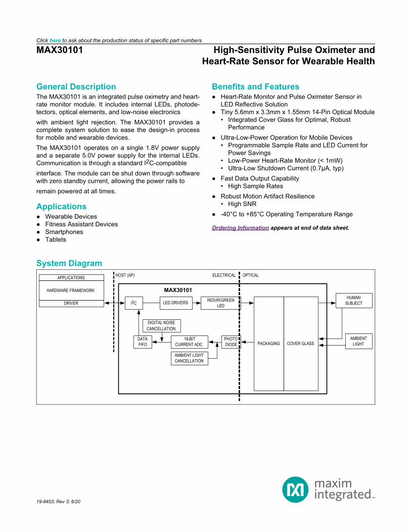
General DescriptionThe MAX30101 is an integrated pulse oximetry and heart-rate monitor module. It includes internal LEDs, photode-tectors, optical elements, and low-noise electronicswith ambient light rejection. The MAX30101 provides acomplete system solution to ease the design-in processfor mobile and wearable devices.The MAX30101 operates on a single 1.8V power supplyand a separate 5.0V power supply for the internal LEDs.Communication is through a standard I2C-compatibleinterface. The module can be shut down through softwarewith zero standby current, allowing the power rails toremain powered at all times.
Applications Wearable Devices Fitness Assistant Devices Smartphones Tablets
Benefits and Features Heart-Rate Monitor and Pulse Oximeter Sensor in
LED Reflective Solution Tiny 5.6mm x 3.3mm x 1.55mm 14-Pin Optical Module
• Integrated Cover Glass for Optimal, RobustPerformance
Ultra-Low-Power Operation for Mobile Devices• Programmable Sample Rate and LED Current for
Power Savings• Low-Power Heart-Rate Monitor (< 1mW)• Ultra-Low Shutdown Current (0.7μA, typ)
Fast Data Output Capability• High Sample Rates
Robust Motion Artifact Resilience• High SNR
-40°C to +85°C Operating Temperature Range
Ordering Information appears at end of data sheet.
System Diagram
PHOTO DIODE
LED DRIVERS RED/IR/GREEN LED
PACKAGING
HUMAN SUBJECT
ELECTRICAL OPTICAL
AMBIENT LIGHT
18-BIT CURRENT ADC
AMBIENT LIGHT CANCELLATION
DIGITAL NOISE CANCELLATION
DATA FIFO
HOST (AP)
I2CDRIVER
HARDWARE FRAMEWORK
APPLICATIONS
COVER GLASS
MAX30101
Click here to ask about the production status of specific part numbers.
MAX30101 High-Sensitivity Pulse Oximeter andHeart-Rate Sensor for Wearable Health
19-8453; Rev 3; 6/20

Absolute Maximum RatingsVDD to GND........................................................... -0.3V to +2.2VGND to PGND ....................................................... -0.3V to +0.3VVLED+ to PGND .................................................... -0.3V to +6.0VAll Other Pins to GND ........................................... -0.3V to +6.0VOutput Short-Circuit Current Duration ........................ ContinuousContinuous Input Current into Any Terminal ..................... ±20mA
Continuous Power Dissipation (TA = +70°C) OESIP (derate5.5mW/°C above +70°C) ..................................................440mWOperating Temperature Range .............................-40°C to +85°CJunction Temperature .........................................................+90°CSoldering Temperature (reflow) ........................................ +260ºCStorage Temperature Range .............................. -40ºC to +105ºC
Stresses beyond those listed under “Absolute Maximum Ratings” may cause permanent damage to the device. These are stress ratings only, and functional operation of thedevice at these or any other conditions beyond those indicated in the operational sections of the specifications is not implied. Exposure to absolute maximum rating conditions forextended periods may affect device reliability.
Package Information
14 OESIPPackage Code F143A5+1Outline Number 21-1048Land Pattern Number 90-0602THERMAL RESISTANCE, FOUR-LAYER BOARDJunction-to-Ambient (θJA) 180°C/WJunction-to-Case Thermal Resistance (θJC) 150°C/W
For the latest package outline information and land patterns (footprints), go to www.maximintegrated.com/packages.Note that a “+”, “#”, or “-” in the package code indicates RoHS status only. Package drawings may show a differentsuffix character, but the drawing pertains to the package regardless of RoHS status.Package thermal resistances were obtained using the method described in JEDEC specification JESD51-7, using afour-layer board. For detailed information on package thermal considerations, refer to www.maximintegrated.com/thermal-tutorial.
Electrical Characteristics(VDD = 1.8V, VLED+ = 5.0V, TA = +25°C, min/max are from TA = -40°C to +85°C, unless otherwise noted. Typical values are at TA =25°C.) (Note 1)
PARAMETER SYMBOL CONDITIONS MIN TYP MAX UNITSPOWER SUPPLY
Power-Supply Voltage VDDGuaranteed by RED and IR counttolerance 1.7 1.8 2.0 V
LED Supply VoltageVLED+ to PGND VLED+
Guaranteed by PSRR of LED driver (REDand IR LED only) 3.1 3.3 5.0
VGuaranteed by PSRR of LED driver(GREEN LED only). TA = 25°C 4.5 5.0 5.5
Supply Current IDDSpO2 and HR mode, PW = 215µs, 50sps 600 1100
µAIR only mode, PW = 215µS, 50sps 600 1100
Supply Current inShutdown ISHDN TA = +25°C, MODE = 0x80 0.7 2.5 µA
PULSE OXIMETRY/HEART-RATE SENSOR CHARACTERISTICSADC Resolution 18 bits
MAX30101 High-Sensitivity Pulse Oximeter andHeart-Rate Sensor for Wearable Health
www.maximintegrated.com19-8453
Maxim Integrated | 2

Electrical Characteristics (continued)(VDD = 1.8V, VLED+ = 5.0V, TA = +25°C, min/max are from TA = -40°C to +85°C, unless otherwise noted. Typical values are at TA =25°C.) (Note 1)
PARAMETER SYMBOL CONDITIONS MIN TYP MAX UNITS
Red ADC Count (Note2) REDC
LED1_PA = 0x0C, LED_PW = 0x01,SPO2_SR = 0x05,ADC_RGE = 0x00
65536 Counts
IR ADC Count (Note 2) IRCLED2_PA = 0x0C, LED_PW = 0x01,SPO2_SR = 0x05ADC_RGE = 0x00
65536 Counts
Green ADC Count (Note2) GRNC
LED3_PA = LED4_PA = 0x24, LED_PW= 0x01,SPO2_SR = 0x05, ADC_RGE = 0x00
65536 Counts
Dark Current Count LED_DCC
LED1_PA = LED2_PA = 0x00, LED_PW= 0x03, SPO2_SR = 0x01 ADC_RGE =0x02
30 128 Counts
LED1_PA = LED2_PA = 0x00, LED_PW= 0x03, SPO2_SR = 0x01 ADC_RGE =0x03
0.01 0.05 % of FS
DC Ambient LightRejection (Note 3) ALR
ADC counts withfinger on sensorunder directsunlight (100K lux),ADC_RGE = 0x3,LED_PW = 0x03,SPO2_SR = 0x01
Red LED 2
CountsADC counts withfinger on sensorunder directsunlight (100K lux),ADC_RGE = 0x3,LED_PW = 0x03,SPO2_SR = 0x02
IR LED 2
ADC Count—PSRR(VDD) PSRRVDD
1.7V < VDD < 2.0V,LED_PW = 0x00, SPO2_SR = 0x05 0.25 1 % of FS
Frequency = DC to 100kHz, 100mVP-P 10 LSB
ADC Count—PSRR(LED Driver Outputs) PSRRLED
3.1V < VLED+ < 5.0V, LED1_PA =LED2_PA = 0x0C,LED_PW = 0x01, SPO2_SR = 0x05
0.05 1
% of FS4.5V < VLED+ < 5.5V, TA = 25°CLED3_PA = LED4_PA = 0x24, LED_PW= 0x01, SPO2_SR = 0x05
0.05 1
Frequency = DC to 100kHz, 100mVP-P 10 LSBADC Clock Frequency CLK 10.2 10.48 10.8 MHz
ADC Integration Time(Note 3) INT
LED_PW = 0x00 69
µsLED_PW = 0x01 118LED_PW = 0x02 215LED_PW = 0x03 411
MAX30101 High-Sensitivity Pulse Oximeter andHeart-Rate Sensor for Wearable Health
www.maximintegrated.com19-8453
Maxim Integrated | 3
Electrical Characteristics (continued)(VDD = 1.8V, VLED+ = 5.0V, TA = +25°C, min/max are from TA = -40°C to +85°C, unless otherwise noted. Typical values are at TA =25°C.) (Note 1)
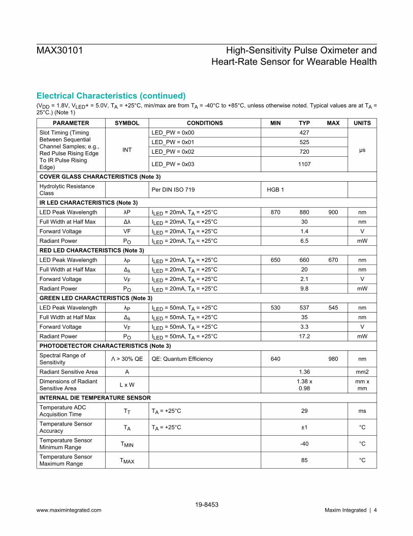
PARAMETER SYMBOL CONDITIONS MIN TYP MAX UNITSSlot Timing (TimingBetween SequentialChannel Samples; e.g.,Red Pulse Rising EdgeTo IR Pulse RisingEdge)
INT
LED_PW = 0x00 427
µsLED_PW = 0x01 525LED_PW = 0x02 720
LED_PW = 0x03 1107
COVER GLASS CHARACTERISTICS (Note 3)Hydrolytic ResistanceClass Per DIN ISO 719 HGB 1
IR LED CHARACTERISTICS (Note 3)LED Peak Wavelength λP ILED = 20mA, TA = +25°C 870 880 900 nmFull Width at Half Max Δλ ILED = 20mA, TA = +25°C 30 nmForward Voltage VF ILED = 20mA, TA = +25°C 1.4 VRadiant Power PO ILED = 20mA, TA = +25°C 6.5 mWRED LED CHARACTERISTICS (Note 3)LED Peak Wavelength λP ILED = 20mA, TA = +25°C 650 660 670 nmFull Width at Half Max Δλ ILED = 20mA, TA = +25°C 20 nmForward Voltage VF ILED = 20mA, TA = +25°C 2.1 VRadiant Power PO ILED = 20mA, TA = +25°C 9.8 mWGREEN LED CHARACTERISTICS (Note 3)LED Peak Wavelength λP ILED = 50mA, TA = +25°C 530 537 545 nmFull Width at Half Max Δλ ILED = 50mA, TA = +25°C 35 nmForward Voltage VF ILED = 50mA, TA = +25°C 3.3 VRadiant Power PO ILED = 50mA, TA = +25°C 17.2 mWPHOTODETECTOR CHARACTERISTICS (Note 3)Spectral Range ofSensitivity Λ > 30% QE QE: Quantum Efficiency 640 980 nm
Radiant Sensitive Area A 1.36 mm2Dimensions of RadiantSensitive Area L x W 1.38 x
0.98mm xmm
INTERNAL DIE TEMPERATURE SENSORTemperature ADCAcquisition Time TT TA = +25°C 29 ms
Temperature SensorAccuracy TA TA = +25°C ±1 °C
Temperature SensorMinimum Range TMIN -40 °C
Temperature SensorMaximum Range TMAX 85 °C
MAX30101 High-Sensitivity Pulse Oximeter andHeart-Rate Sensor for Wearable Health
www.maximintegrated.com19-8453
Maxim Integrated | 4

Electrical Characteristics (continued)(VDD = 1.8V, VLED+ = 5.0V, TA = +25°C, min/max are from TA = -40°C to +85°C, unless otherwise noted. Typical values are at TA =25°C.) (Note 1)
PARAMETER SYMBOL CONDITIONS MIN TYP MAX UNITSDIGITAL INPUTS (SCL, SDA)
Input Logic-Low Voltage VIL0.3 xVDD
V
Input Logic-High Voltage VIH0.7 xVDD
V
Input Hysteresis VHYS0.5 xVDD
V
Input Leakage Current IIN ±0.1 ±1 µAInput Capacitance CIN 10 pFDIGITAL OUTPUTS (SDA, INT)Output Low Voltage VOL ISINK = 3mA 0.4 VI2C TIMING CHARACTERISTICSI2C Write Address AE HexI2C Read Address AF HexSCL Clock Frequency fSCL Lower limit not tested 0 400 kHzBus Free Time BetweenSTOP and STARTCondition
tBUF 1.3 µs
Hold Time (Repeated)START Condition tHD,STA 0.6 µs
SCL Pulse-Width Low tLOW 1.3 µsSCL Pulse-Width High tHIGH 0.6 µsSetup Time for aRepeated STARTCondition
tSU,STA 0.6 µs
Data Hold Time tHD;DAT 0 0.9 µsData Setup Time tSU;DAT 100 nsSetup Time for STOPCondition tSU;STO 0.6 µs
Pulse Width ofSuppressed Spike tSP 50 ns
Bus Capacitance Cb 400 pFSDA and SCL ReceivingRise Time Tr (Note 4) 20 300 ns
SDA and SCL ReceivingFall Time tRf (Note 4) 20 x
VDD/5.5 300 ns
SDA Transmitting FallTime tof
20 xVDD/5.5 250 ns
Note 1: All devices are 100% production tested at TA = +25°C. Specifications over temperature limits are guaranteed by MaximIntegrated’s bench or proprietary automated test equipment (ATE) characterization.
Note 2: Specifications are guaranteed by Maxim Integrated’s bench characterization and by 100% production test using proprietaryATE setup and conditions.
MAX30101 High-Sensitivity Pulse Oximeter andHeart-Rate Sensor for Wearable Health
www.maximintegrated.com19-8453
Maxim Integrated | 5
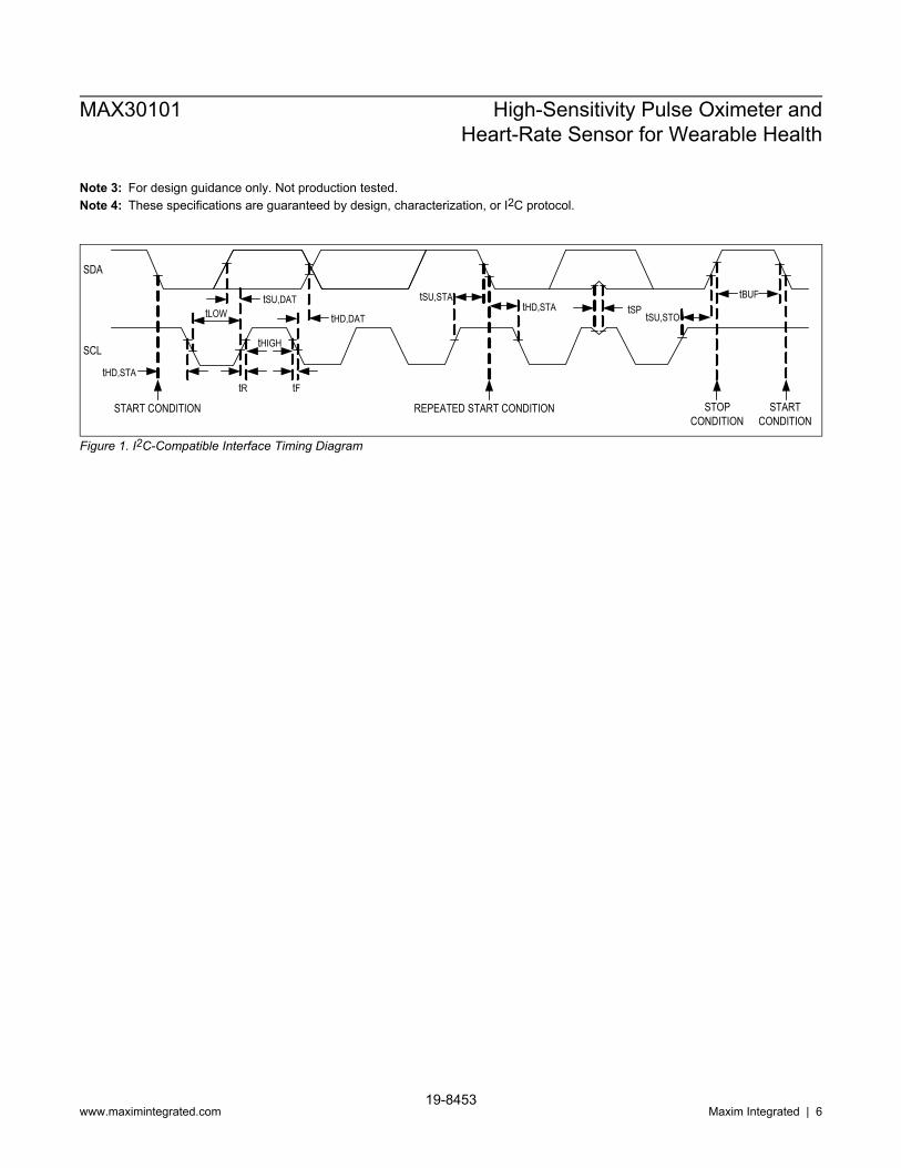
Note 3: For design guidance only. Not production tested.Note 4: These specifications are guaranteed by design, characterization, or I2C protocol.
SDA
SCL
tHD,STA
START CONDITION
tR tF
tLOWtSU,DAT
tHD,DAT
tSU,STAtHD,STA
REPEATED START CONDITION
tSP tSU,STO
tBUF
STOPCONDITION
STARTCONDITION
tHIGH
Figure 1. I2C-Compatible Interface Timing Diagram
MAX30101 High-Sensitivity Pulse Oximeter andHeart-Rate Sensor for Wearable Health
www.maximintegrated.com19-8453
Maxim Integrated | 6
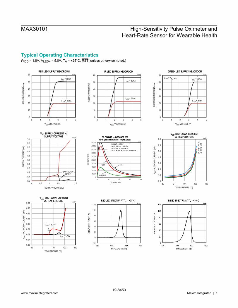
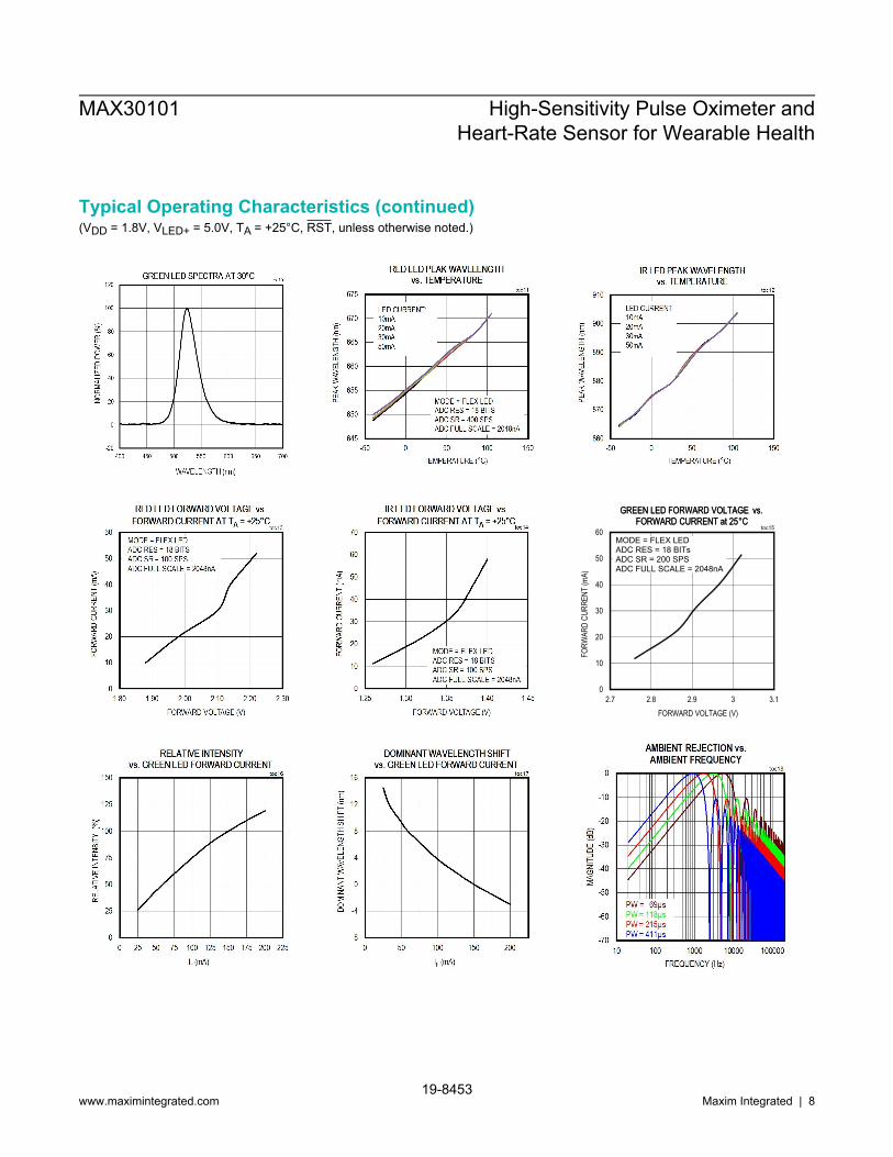
Typical Operating Characteristics(VDD = 1.8V, VLED+ = 5.0V, TA = +25°C, RST, unless otherwise noted.)
0
10
20
30
40
50
60
0 1 2 3 4 5
RED
LED
CURR
ENT
(mA)
VLED VOLTAGE (V)
REDRED LEDLED SUPPLYSUPPLY HEADROOMHEADROOMtoc01
ILED = 50mA
ILED = 20mA
0
10
20
30
40
50
60
0 1 2 3 4 5
IR LE
D CU
RREN
T (m
A)
VLED VOLTAGE (V)
IRIR LEDLED SUPPLYSUPPLY HEADROOMHEADROOMtoc02
ILED = 50mA
ILED = 20mA
0
10
20
30
40
50
60
0 1 2 3 4 5
GREE
N LE
D CU
RREN
T (m
A)
VLED VOLTAGE (V)
GREENGREEN LEDLED SUPPLYSUPPLY HEADROOMHEADROOMtoc03
ILED = 50mA
ILED = 20mA
VLED = VX_DRV
0.0
0.1
0.2
0.3
0.4
0.5
0.6
0.7
0.8
0.9
1.0
0 0.5 1 1.5 2 2.5
SUPP
LY C
URRE
NT (m
A)
SUPPLY VOLTAGE (V)
VVDDDD SUPPLYSUPPLY CURRENTCURRENT vsvs..SUPPLYSUPPLY VOLTAGEVOLTAGE toc04
SHUTDOWN MODE
0
5000
10000
15000
20000
25000
30000
35000
40000
45000
50000
0 5 10 15 20
COUN
TS (S
UM)
DISTANCE (mm)
DCDC COUNTSCOUNTS vs.vs. DISTANCEDISTANCE FORFORWHITEWHITE HIGHHIGH IMPACTIMPACT STYRENESTYRENE CARDCARD
toc05
GREEN
IR
MODE = SPO2 and HRADC RES = 18 BITsADC SR = 100 SPSADC FULL SCALE = 16384nA
DCDC COUNTSCOUNTS vs.vs. DISTANCEDISTANCE FORFORWHITEWHITE HIGHHIGH IMPACTIMPACT STYRENESTYRENE CARDCARD
RED
MODE = LEDADC RES = 18 BITsADC SR = 100 SPSADC FULL SCALE = 16384nA
0.0
1.0
2.0
3.0
4.0
5.0
6.0
7.0
-50 0 50 100 150
V DDSH
UTDO
WN
CURR
ENT
(µA)
TEMPERATURE (°C)
VVDDDD SHUTDOWNSHUTDOWN CURRENTCURRENTvs.vs. TEMPERATURETEMPERATURE toc06
VDD2.2V 2.0V 1.8V 1.7V
0.06
0.07
0.08
0.09
0.10
0.11
0.12
0.13
0.14
-50 0 50 100 150
V LED
SHUT
DOW
N CU
RREN
T (µ
A)
TEMPERATURE (°C)
VVLEDLED SHUTDOWNSHUTDOWN CURRENTCURRENTvs.vs. TEMPERATURETEMPERATURE
VLED = 4.75V
toc07
VLED = 5.25V
MAX30101 High-Sensitivity Pulse Oximeter andHeart-Rate Sensor for Wearable Health
www.maximintegrated.com19-8453
Maxim Integrated | 7
Typical Operating Characteristics (continued)(VDD = 1.8V, VLED+ = 5.0V, TA = +25°C, RST, unless otherwise noted.)
0
10
20
30
40
50
60
2.7 2.8 2.9 3 3.1
FORW
ARD
CURR
ENT
(mA)
FORWARD VOLTAGE (V)
GREENGREEN LEDLED FORWARDFORWARD VOLTAGEVOLTAGE vs.vs.FORWARDFORWARD CURRENTCURRENT atat 2525°°CC
toc15
MODE = FLEX LEDADC RES = 18 BITsADC SR = 200 SPSADC FULL SCALE = 2048nA
MAX30101 High-Sensitivity Pulse Oximeter andHeart-Rate Sensor for Wearable Health
www.maximintegrated.com19-8453
Maxim Integrated | 8

Typical Operating Characteristics (continued)(VDD = 1.8V, VLED+ = 5.0V, TA = +25°C, RST, unless otherwise noted.)
Pin Configuration
N.C. 1
SCL 2
SDA 3
PGND 4
N.C. 5
N.C. 6
N.C. 7
14 N.C.
13 INT
12 GND
11 VDD
10 VLED+
9 VLED+
8 N.C.
SENSOR
LED
MAX30101
Pin DescriptionPIN NAME FUNCTION
1, 5, 6, 7, 8,14 N.C. No Connection. Connect to PCB pad for mechanical stability.
2 SCL I2C Clock Input3 SDA I2C Clock Data, Bidirectional (Open-Drain)4 PGND Power Ground of the LED Driver Blocks
9, 10 VLED+ LED Power Supply (anode connection). Use a bypass capacitor to PGND for best performance.11 VDD Analog Power Supply Input. Use a bypass capacitor to GND for best performance.12 GND Analog Ground13 INT Active-Low Interrupt (Open-Drain). Connect to an external voltage with a pullup resistor.
MAX30101 High-Sensitivity Pulse Oximeter andHeart-Rate Sensor for Wearable Health
www.maximintegrated.com19-8453
Maxim Integrated | 9

Functional Diagrams
880nm660nm
ADC
AMBIENT LIGHT CANCELLATION ANALOG
ADCDIE TEMP
OSCILLATOR
DIGITAL FILTER
DIGITAL
DATAREGISTER
LED DRIVERS
I2CCOMMUNICATION INT
SDA
SCL
VDDVLED+
N.C.N.C. GND PGND
RED IR
VISIBLE+IR
MAX30101
GREEN
527nm
N.C.
MAX30101 High-Sensitivity Pulse Oximeter andHeart-Rate Sensor for Wearable Health
www.maximintegrated.com19-8453
Maxim Integrated | 10
Detailed DescriptionThe MAX30101 is a complete pulse oximetry and heart- rate sensor system solution module designed for the demandingrequirements of wearable devices. The MAX30101 maintains a very small solution size without sacrificing optical orelectrical performance. Minimal external hardware components are required for integra- tion into a wearable system.The MAX30101 is fully adjustable through software regis- ters, and the digital output data can be stored in a 32-deepFIFO within the IC. The FIFO allows the MAX30101 to be connected to a microcontroller or processor on a shared bus,where the data is not being read continuously from the MAX30101’s registers.
SpO2 SubsystemThe SpO2 subsystem contains ambient light cancellation (ALC), a continuous-time sigma-delta ADC, and propri- etarydiscrete time filter. The ALC has an internal Track/ Hold circuit to cancel ambient light and increase the effec- tive dynamicrange. The SpO2 ADC has a programmable full-scale ranges from 2µA to 16µA. The ALC can cancel up to 200µA ofambient current.The internal ADC is a continuous time oversampling sigma-delta converter with 18-bit resolution. The ADC sampling rateis 10.24MHz. The ADC output data rate can be programmed from 50sps (samples per second) to 3200sps.
Temperature SensorThe MAX30101 has an on-chip temperature sensor for calibrating the temperature dependence of the SpO2 subsystem.The temperature sensor has an inherent resolution 0.0625°C.The device output data is relatively insensitive to the wavelength of the IR LED, where the red LED’s wave- length iscritical to correct interpretation of the data. An SpO2 algorithm used with the MAX30101 output signal can compensatefor the associated SpO2 error with ambient temperature changes.
LED DriverThe MAX30101 integrates red, green, and IR LED drivers to modulate LED pulses for SpO2 and HR measurements. TheLED current can be programmed from 0 to 50mA with proper supply voltage. The LED pulse width can be programmedfrom 69µs to 411µs to allow the algorithm to optimize SpO2 and HR accuracy and power consumptionbased on use cases.
MAX30101 High-Sensitivity Pulse Oximeter andHeart-Rate Sensor for Wearable Health
www.maximintegrated.com19-8453
Maxim Integrated | 11

Register Maps and DescriptionsREGISTER B7 B6 B5 B4 B3 B2 B1 B0 REG
ADDRPOR
STATER/W
STATUSInterrupt Status 1 A_FULL PPG_
RDYALC_OVF
PWR_RDY
0x00 0X00 R
Interrupt Status 2 DIE_TEMP_RDY 0x01
0x00 R
Interrupt Enable 1 A_FULL_EN
PPG_RDY_EN
ALC_OVF_EN
0x02 0X00 R/W
Interrupt Enable 2 DIE_TEMP_RDY_EN
0x03 0x00 R/W
FIFOFIFO Write Pointer FIFO_WR_PTR[4:0] 0x04 0x00 R/
WOverflowCounter
OVF_COUNTER[4:0] 0x05 0x00 R/W
FIFO Read Pointer FIFO_RD_PTR[4:0] 0x06 0x00 R/W
FIFO Data Register FIFO_DATA[7:0] 0x07 0x00 R/W
CONFIGURATIONFIFOConfiguration
SMP_AVE[2:0] FIFO_ ROLLOVER_EN
FIFO_A_FULL[3:0]0x08
0x00 R/W
ModeConfiguration
SHDN RESET MODE[2:0] 0x09 0x00 R/W
SpO2Configuration
0(Reserved)
SPO2_ADC_RGE[1:0]
SPO2_SR[2:0] LED_PW[1:0] 0x0A 0x00 R/W
RESERVED 0x0B 0x00 R/W
LED PulseAmplitude
LED1_PA[7:0] 0x0C 0x00 R/W
LED2_PA[7:0] 0x0D 0x00 R/W
LED3_PA[7:0] 0x0E 0x00 R/W
LED4_PA[7:0] 0x0F 0x00 R/W
Multi-LED ModeControl Registers
SLOT2[2:0] SLOT1[2:0] 0x11 0x00 R/W
SLOT4[2:0] SLOT3[2:0] 0x12 0x00 R/W
RESERVED 0x13–0x17
0xFF R/W
RESERVED 0x18-0x1E
0x00 R
DIE TEMPERATURE
MAX30101 High-Sensitivity Pulse Oximeter andHeart-Rate Sensor for Wearable Health
www.maximintegrated.com19-8453
Maxim Integrated | 12
REGISTER B7 B6 B5 B4 B3 B2 B1 B0 REGADDR
PORSTATE
R/W
Die Temp Integer TINT[7:0] 0x1F 0x00 RDie Temp Fraction TFRAC[3:0] 0x20 0x00 RDie TemperatureConfig
TEMP_EN 0x21
0x00 R/W
RESERVED 0x22–0x2F
0x00 R/W
PART IDRevision ID REV_ID[7:0] 0xFE 0xXX* RPart ID PART_ID[7] 0xFF 0x15 R
*XX denotes a 2-digit hexadecimal number (00 to FF) for part revision identification. Contact Maxim Integrated for therevision ID number assigned for your product.
Interrupt Status (0x00–0x01)
REGISTER B7 B6 B5 B4 B3 B2 B1 B0 REGADDR
PORSTATE
R/W
Interrupt Status1
A_FULL PPG_RDY ALC_OVF PWR_RDY
0x00 0X00 R
Interrupt Status2
DIE_TEMP_RDY
0x01 0x00 R
Whenever an interrupt is triggered, the MAX30101 pulls the active-low interrupt pin into its low state until the interrupt iscleared.
A_FULL: FIFO Almost Full FlagIn SpO2 and HR modes, this interrupt triggers when the FIFO write pointer has a certain number of free spacesremaining. The trigger number can be set by the FIFO_A_FULL[3:0] register. The interrupt is cleared by reading theInterrupt Status 1 register (0x00).
PPG_RDY: New FIFO Data ReadyIn SpO2 and HR modes, this interrupt triggers when there is a new sample in the data FIFO. The interrupt is cleared byreading the Interrupt Status 1 register (0x00), or by reading the FIFO_DATA register.
ALC_OVF: Ambient Light Cancellation OverflowThis interrupt triggers when the ambient light cancellation function of the SpO2/HR photodiode has reached its maximumlimit, and therefore, ambient light is affecting the output of the ADC. The interrupt is cleared by reading the InterruptStatus 1 register (0x00).
PWR_RDY: Power Ready FlagOn power-up or after a brownout condition, when the supply voltage VDD transitions from below the undervoltage lockout(UVLO) voltage to above the UVLO voltage, a power-ready interrupt is triggered to signal that the module is powered-upand ready to collect data.
DIE_TEMP_RDY: Internal Temperature Ready FlagWhen an internal die temperature conversion is finished, this interrupt is triggered so the processor can read thetemperature data registers. The interrupt is cleared by reading either the Interrupt Status 2 register (0x01) or the TFRACregister (0x20).
MAX30101 High-Sensitivity Pulse Oximeter andHeart-Rate Sensor for Wearable Health
www.maximintegrated.com19-8453
Maxim Integrated | 13

The interrupts are cleared whenever the interrupt status register is read, or when the register that triggered the interruptis read. For example, if the SpO2 sensor triggers an interrupt due to finishing a conversion, reading either the FIFO dataregister or the interrupt register clears the interrupt pin (which returns to its normal HIGH state). This also clears all thebits in the interrupt status register to zero.
Interrupt Enable (0x02-0x03)
REGISTER B7 B6 B5 B4 B3 B2 B1 B0 REGADDR
PORSTATE
R/W
InterruptEnable 1
A_ FULL_EN
PPG_RDY_EN
ALC_OVF_EN
0x02 0X00 R/W
InterruptEnable 2
DIE_TEMP_RDY_EN
0x03 0x00 R/W
Each source of hardware interrupt, with the exception of power ready, can be disabled in a software register within theMAX30101 IC. The power-ready interrupt cannot be disabled because the digital state of the module is reset upon abrownout condition (low power supply voltage), and the default condition is that all the interrupts are disabled. Also, it isimportant for the system to know that a brownout condition has occurred, and the data within the module is reset as aresult.The unused bits should always be set to zero for normal operation.
FIFO (0x04–0x07)
REGISTER B7 B6 B5 B4 B3 B2 B1 B0 REG ADDR POR STATE R/WFIFO Write Pointer FIFO_WR_PTR[4:0] 0x04 0x00 R/WOver Flow Counter OVF_COUNTER[4:0] 0x05 0x00 R/WFIFO Read Pointer FIFO_RD_PTR[4:0] 0x06 0x00 R/WFIFO Data Register FIFO_DATA[7:0] 0x07 0x00 R/W
FIFO Write PointerThe FIFO Write Pointer points to the location where the MAX30101 writes the next sample. This pointer advances foreach sample pushed on to the FIFO. It can also be changed through the I2C interface when MODE[2:0] is 010, 011, or111.
FIFO Overflow CounterWhen the FIFO is full, samples are not pushed on to the FIFO, samples are lost. OVF_COUNTER counts the number ofsamples lost. It saturates at 0x1F. When a complete sample is “popped” (i.e., removal of old FIFO data and shifting thesamples down) from the FIFO (when the read pointer advances), OVF_COUNTER is reset to zero.
FIFO Read PointerThe FIFO Read Pointer points to the location from where the processor gets the next sample from the FIFO through theI2C interface. This advances each time a sample is popped from the FIFO. The processor can also write to this pointerafter reading the samples to allow rereading samples from the FIFO if there is a data communication error.
FIFO Data RegisterThe circular FIFO depth is 32 and can hold up to 32 samples of data. The sample size depends on the number of LEDchannels (a.k.a. channels) configured as active. As each channel signal is stored as a 3-byte data signal, the FIFO widthcan be 3 bytes, 6 bytes, 9 bytes, or 12 bytes in size. The FIFO_DATA register in the I2C register map points to thenext sample to be read from the FIFO. FIFO_RD_PTR points to this sample. Reading FIFO_DATA register, does notautomatically increment the I2C register address. Burst reading this register, reads the same address over and over.
MAX30101 High-Sensitivity Pulse Oximeter andHeart-Rate Sensor for Wearable Health
www.maximintegrated.com19-8453
Maxim Integrated | 14

Each sample is 3 bytes of data per channel (i.e., 3 bytes for RED, 3 bytes for IR, etc.). The FIFO registers (0x04–0x07)can all be written and read, but in practice only the FIFO_RD_PTR register should be written to in operation. The othersare automatically incremented or filled with data by the MAX30101. When starting a new SpO2 or heart rate conversion, itis recommended to first clear the FIFO_WR_PTR, OVF_COUNTER, and FIFO_RD_PTR registers to all zeroes (0x00) toensure the FIFO is empty and in a known state. When reading the MAX30101 registers in one burst-read I2C transaction,the register address pointer typically increments so that the next byte of data sent is from the next register, etc. Theexception to this is the FIFO data register, register 0x07. When reading this register, the address pointer does notincrement, but the FIFO_RD_PTR does. So the next byte of data sent represents the next byte of data available in theFIFO.
Reading from the FIFONormally, reading registers from the I2C interface autoincrements the register address pointer, so that all the registerscan be read in a burst read without an I2C start event. In the MAX30101, this holds true for all registers except for theFIFO_DATA register (register 0x07). Reading the FIFO_DATA register does not automatically increment the registeraddress. Burst reading this register reads data from the same address over and over. Each sample comprises multiplebytes of data, so multiple bytes should be read from this register (in the same transaction) to get one full sample. Theother exception is 0xFF. Reading more bytes after the 0xFF register does not advance the address pointer back to 0x00,and the data read is not meaningful.
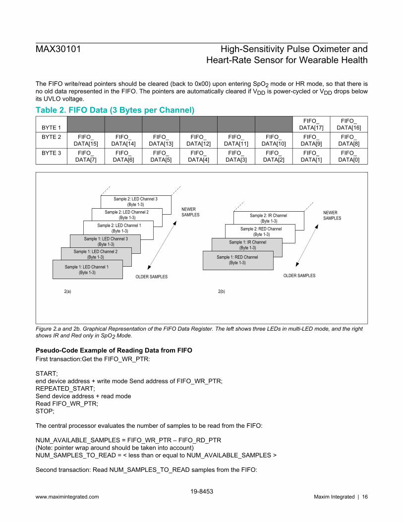
FIFO Data StructureThe data FIFO consists of a 32-sample memory bank that can store GREEN, IR, and RED ADC data. Since each sampleconsists of three channels of data, there are 9 bytes of data for each sample, and therefore 288 total bytes of data canbe stored in the FIFO.The FIFO data is left-justified, as shown in Table 1; in other words, the MSB bit is always in the bit 17 data position,regardless of ADC resolution setting. See Table 2 for a visual presentation of the FIFO data structure.
Table 1. FIFO Data is Left-Justified
ADCResolution …
18-bit17-bit16-bit15-bit
FIFO Data Contains 3 Bytes per ChannelThe FIFO data is left-justified, meaning that the MSB is always in the same location regardless of the ADC resolutionsetting. FIFO DATA[18] – [23] are not used. Table 2 shows the structure of each triplet of bytes (containing the 18-bitADC data output of each channel). Each data sample in SpO2 mode comprises two data triplets (3 bytes each), To readone sample, requires an I2C read command for each byte. Thus, to read one sample in SpO2 mode, requires 6 I2C bytereads. To read one sample with three LED channels requires 9 I2C byte reads. The FIFO read pointer is automaticallyincremented after the first byte of each sample is read.
Write/Read PointersWrite/Read pointers are used to control the flow of data in the FIFO. The write pointer increments every time a newsample is added to the FIFO. The read pointer is incremented every time a sample is read from the FIFO. To reread asample from the FIFO, decrement its value by one and read the data register again.
FIFO
_DA
TA[1
7]
FIFO
_DA
TA[1
6]
FIFO
_DA
TA[1
2]
FIFO
_DA
TA[1
1]
FIFO
_DA
TA[1
0]
FIFO
_DA
TA[9
]
FIFO
_DA
TA[8
]
FIFO
_DA
TA[7
]
FIFO
_DA
TA[6
]
FIFO
_DA
TA[5
]
FIFO
_DA
TA[4
]
FIFO
_DA
TA[3
]
FIFO
_DA
TA[2
]
FIFO
_DA
TA[1
]
FIFO
_DA
TA[0
]
MAX30101 High-Sensitivity Pulse Oximeter andHeart-Rate Sensor for Wearable Health
www.maximintegrated.com19-8453
Maxim Integrated | 15
The FIFO write/read pointers should be cleared (back to 0x00) upon entering SpO2 mode or HR mode, so that there isno old data represented in the FIFO. The pointers are automatically cleared if VDD is power-cycled or VDD drops belowits UVLO voltage.
Table 2. FIFO Data (3 Bytes per Channel)
BYTE 1FIFO_
DATA[17]FIFO_
DATA[16]BYTE 2 FIFO_
DATA[15]FIFO_
DATA[14]FIFO_
DATA[13]FIFO_
DATA[12]FIFO_
DATA[11]FIFO_
DATA[10]FIFO_
DATA[9]FIFO_
DATA[8]BYTE 3 FIFO_
DATA[7]FIFO_
DATA[6]FIFO_
DATA[5]FIFO_
DATA[4]FIFO_
DATA[3]FIFO_
DATA[2]FIFO_
DATA[1]FIFO_
DATA[0]
Sample 2: LED Channel 1 (Byte 1-3)
Sample 2: LED Channel 2 (Byte 1-3)
NEWER SAMPLES
2(a)
Sample 2: LED Channel 3 (Byte 1-3)
Sample 1: LED Channel 3 (Byte 1-3)
Sample 1: LED Channel 1 (Byte 1-3)
Sample 1: LED Channel 2 (Byte 1-3)
2(b)
OLDER SAMPLES
Sample 2: RED Channel (Byte 1-3)
Sample 2: IR Channel (Byte 1-3)
NEWER SAMPLES
Sample 1: IR Channel (Byte 1-3)
Sample 1: RED Channel (Byte 1-3)
OLDER SAMPLES
Figure 2.a and 2b. Graphical Representation of the FIFO Data Register. The left shows three LEDs in multi-LED mode, and the rightshows IR and Red only in SpO2 Mode.
Pseudo-Code Example of Reading Data from FIFOFirst transaction:Get the FIFO_WR_PTR:
START;end device address + write mode Send address of FIFO_WR_PTR;REPEATED_START;Send device address + read modeRead FIFO_WR_PTR;STOP;
The central processor evaluates the number of samples to be read from the FIFO:
NUM_AVAILABLE_SAMPLES = FIFO_WR_PTR – FIFO_RD_PTR(Note: pointer wrap around should be taken into account)NUM_SAMPLES_TO_READ = < less than or equal to NUM_AVAILABLE_SAMPLES >
Second transaction: Read NUM_SAMPLES_TO_READ samples from the FIFO:
MAX30101 High-Sensitivity Pulse Oximeter andHeart-Rate Sensor for Wearable Health
www.maximintegrated.com19-8453
Maxim Integrated | 16

START;Send device address + write modeSend address of FIFO_DATA;REPEATED_START;Send device address + read modefor (i = 0; i < NUM_SAMPLES_TO_READ; i++) Read FIFO_DATA;Save LED1[23:16];Read FIFO_DATA;Save LED1[15:8];Read FIFO_DATA;Save LED1[7:0];Read FIFO_DATA;Save LED2[23:16];Read FIFO_DATA;Save LED2[15:8];Read FIFO_DATA;Save LED2[7:0];Read FIFO_DATA;Save LED3[23:16];Read FIFO_DATA;Save LED3[15:8];Read FIFO_DATA;Save LED3[7:0];Read FIFO_DATA;STOP;START;Send device address + write modeSend address of FIFO_RD_PTR;
Write FIFO_RD_PTR;STOP;
Third transaction: Write to FIFO_RD_PTR register. If the second transaction was successful, FIFO_RD_PTR pointsto the next sample in the FIFO, and this third transaction is not necessary. Otherwise, the processor updates theFIFO_RD_PTR appropriately, so that the samples are reread.
FIFO Configuration (0x08)REGISTER B7 B6 B5 B4 B3 B2 B1 B0 REG ADDR POR STATE R/W
FIFOConfiguration
SMP_AVE[2:0] FIFO_ROL LOVER_EN FIFO_A_FULL[3:0] 0x08 0x00 R/W
MAX30101 High-Sensitivity Pulse Oximeter andHeart-Rate Sensor for Wearable Health
www.maximintegrated.com19-8453
Maxim Integrated | 17
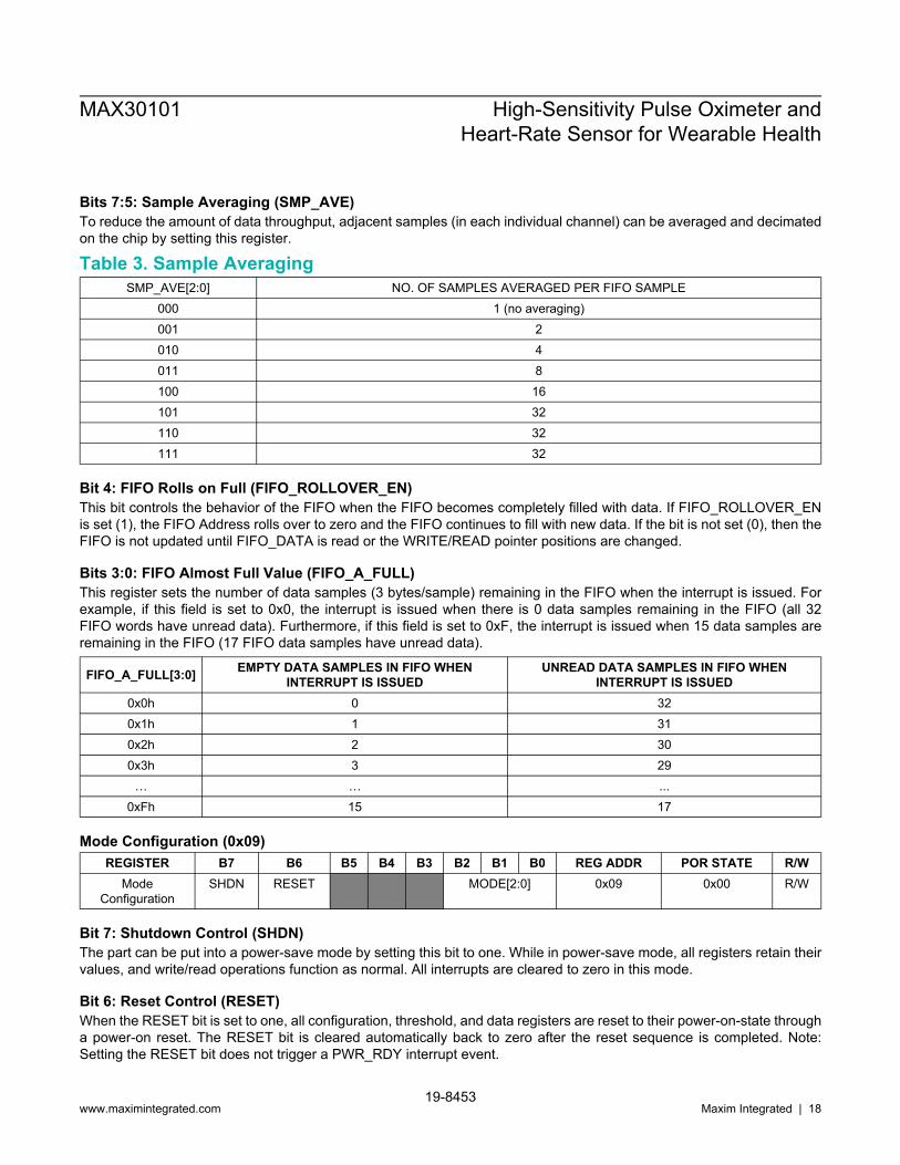
Bits 7:5: Sample Averaging (SMP_AVE)To reduce the amount of data throughput, adjacent samples (in each individual channel) can be averaged and decimatedon the chip by setting this register.
Table 3. Sample AveragingSMP_AVE[2:0] NO. OF SAMPLES AVERAGED PER FIFO SAMPLE
000 1 (no averaging)001 2010 4011 8100 16101 32110 32111 32
Bit 4: FIFO Rolls on Full (FIFO_ROLLOVER_EN)This bit controls the behavior of the FIFO when the FIFO becomes completely filled with data. If FIFO_ROLLOVER_ENis set (1), the FIFO Address rolls over to zero and the FIFO continues to fill with new data. If the bit is not set (0), then theFIFO is not updated until FIFO_DATA is read or the WRITE/READ pointer positions are changed.
Bits 3:0: FIFO Almost Full Value (FIFO_A_FULL)This register sets the number of data samples (3 bytes/sample) remaining in the FIFO when the interrupt is issued. Forexample, if this field is set to 0x0, the interrupt is issued when there is 0 data samples remaining in the FIFO (all 32FIFO words have unread data). Furthermore, if this field is set to 0xF, the interrupt is issued when 15 data samples areremaining in the FIFO (17 FIFO data samples have unread data).
FIFO_A_FULL[3:0] EMPTY DATA SAMPLES IN FIFO WHENINTERRUPT IS ISSUED
UNREAD DATA SAMPLES IN FIFO WHENINTERRUPT IS ISSUED
0x0h 0 320x1h 1 310x2h 2 300x3h 3 29
… … ...0xFh 15 17
Mode Configuration (0x09)REGISTER B7 B6 B5 B4 B3 B2 B1 B0 REG ADDR POR STATE R/W
ModeConfiguration
SHDN RESET MODE[2:0] 0x09 0x00 R/W
Bit 7: Shutdown Control (SHDN)The part can be put into a power-save mode by setting this bit to one. While in power-save mode, all registers retain theirvalues, and write/read operations function as normal. All interrupts are cleared to zero in this mode.
Bit 6: Reset Control (RESET)When the RESET bit is set to one, all configuration, threshold, and data registers are reset to their power-on-state througha power-on reset. The RESET bit is cleared automatically back to zero after the reset sequence is completed. Note:Setting the RESET bit does not trigger a PWR_RDY interrupt event.
MAX30101 High-Sensitivity Pulse Oximeter andHeart-Rate Sensor for Wearable Health
www.maximintegrated.com19-8453
Maxim Integrated | 18
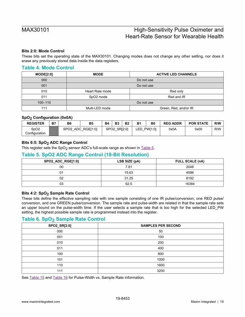
Bits 2:0: Mode ControlThese bits set the operating state of the MAX30101. Changing modes does not change any other setting, nor does iterase any previously stored data inside the data registers.
Table 4. Mode ControlMODE[2:0] MODE ACTIVE LED CHANNELS
000 Do not use001 Do not use010 Heart Rate mode Red only011 SpO2 mode Red and IR
100–110 Do not use111 Multi-LED mode Green, Red, and/or IR
SpO2 Configuration (0x0A)REGISTER B7 B6 B5 B4 B3 B2 B1 B0 REG ADDR POR STATE R/W
SpO2Configuration
SPO2_ADC_RGE[1:0] SPO2_SR[2:0] LED_PW[1:0] 0x0A 0x00 R/W
Bits 6:5: SpO2 ADC Range ControlThis register sets the SpO2 sensor ADC’s full-scale range as shown in Table 5.
Table 5. SpO2 ADC Range Control (18-Bit Resolution)SPO2_ADC_RGE[1:0] LSB SIZE (pA) FULL SCALE (nA)
00 7.81 204801 15.63 409602 31.25 819203 62.5 16384
Bits 4:2: SpO2 Sample Rate ControlThese bits define the effective sampling rate with one sample consisting of one IR pulse/conversion, one RED pulse/conversion, and one GREEN pulse/conversion. The sample rate and pulse-width are related in that the sample rate setsan upper bound on the pulse-width time. If the user selects a sample rate that is too high for the selected LED_PWsetting, the highest possible sample rate is programmed instead into the register.
Table 6. SpO2 Sample Rate ControlSPO2_SR[2:0] SAMPLES PER SECOND
000 50001 100010 200011 400100 800101 1000110 1600111 3200
See Table 15 and Table 16 for Pulse-Width vs. Sample Rate information.
MAX30101 High-Sensitivity Pulse Oximeter andHeart-Rate Sensor for Wearable Health
www.maximintegrated.com19-8453
Maxim Integrated | 19

Bits 1:0: LED Pulse Width Control and ADC ResolutionThese bits set the LED pulse width (the IR, Red, and Green have the same pulse width), and, therefore, indirectly setsthe integration time of the ADC in each sample. The ADC resolution is directly related to the integration time.
Table 7. LED Pulse Width ControlLED_PW[1:0] PULSE WIDTH (µs) ADC RESOLUTION (bits)
00 69 (68.95) 1501 118 (117.78) 1610 215 (215.44) 1711 411 (410.75) 18
LED Pulse Amplitude (0x0C–0x0F)REGISTER B7 B6 B5 B4 B3 B2 B1 B0 REG ADDR POR STATE R/W
LED Pulse Amplitude LED1_PA[7:0] 0x0C 0x00 R/WLED2_PA[7:0] 0x0D 0x00 R/WLED3_PA[7:0] 0x0E 0x00 R/WLED4_PA[7:0] 0x0F 0x00 R/W
These bits set the current level of each LED as shown in Table 8
Table 8. LED Current ControlLEDx_PA [7:0] TYPICAL LED CURRENT (mA)*
0x00h 0.00x01h 0.20x02h 0.4
… …0x0Fh 3.0
… …0x1Fh 6.2
… …0x3Fh 12.6
… …0x7Fh 25.4
… …0xFFh 51.0
.*Actual measured LED current for each part can vary significantly due to the trimming methodology.
Multi-LED Mode Control Registers (0x11–0x12)REGISTER B7 B6 B5 B4 B3 B2 B1 B0 REG ADDR POR STATE R/W
Multi-LED Mode Control Registers SLOT2[2:0] SLOT1[2:0] 0x11 0x00 R/WSLOT4[2:0] SLOT3[2:0] 0x12 0x00 R/W
In multi-LED mode, each sample is split into up to four time slots, SLOT1 through SLOT4. These control registersdetermine which LED is active in each time slot, making for a very flexible configuration.
MAX30101 High-Sensitivity Pulse Oximeter andHeart-Rate Sensor for Wearable Health
www.maximintegrated.com19-8453
Maxim Integrated | 20
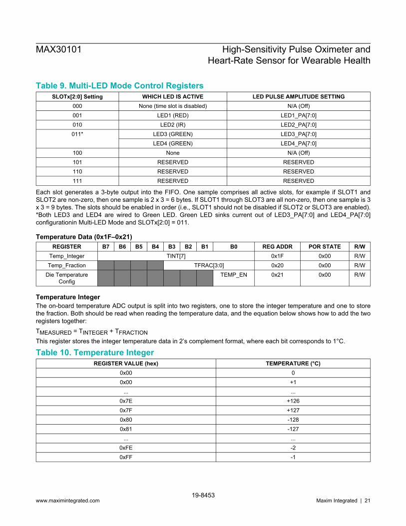
Table 9. Multi-LED Mode Control RegistersSLOTx[2:0] Setting WHICH LED IS ACTIVE LED PULSE AMPLITUDE SETTING
000 None (time slot is disabled) N/A (Off)001 LED1 (RED) LED1_PA[7:0]010 LED2 (IR) LED2_PA[7:0]011* LED3 (GREEN) LED3_PA[7:0]
LED4 (GREEN) LED4_PA[7:0]100 None N/A (Off)101 RESERVED RESERVED110 RESERVED RESERVED111 RESERVED RESERVED
Each slot generates a 3-byte output into the FIFO. One sample comprises all active slots, for example if SLOT1 andSLOT2 are non-zero, then one sample is 2 x 3 = 6 bytes. If SLOT1 through SLOT3 are all non-zero, then one sample is 3x 3 = 9 bytes. The slots should be enabled in order (i.e., SLOT1 should not be disabled if SLOT2 or SLOT3 are enabled).*Both LED3 and LED4 are wired to Green LED. Green LED sinks current out of LED3_PA[7:0] and LED4_PA[7:0]configurationin Multi-LED Mode and SLOTx[2:0] = 011.
Temperature Data (0x1F–0x21)REGISTER B7 B6 B5 B4 B3 B2 B1 B0 REG ADDR POR STATE R/W
Temp_Integer TINT[7] 0x1F 0x00 R/WTemp_Fraction TFRAC[3:0] 0x20 0x00 R/W
Die TemperatureConfig
TEMP_EN 0x21 0x00 R/W
Temperature IntegerThe on-board temperature ADC output is split into two registers, one to store the integer temperature and one to storethe fraction. Both should be read when reading the temperature data, and the equation below shows how to add the tworegisters together:TMEASURED = TINTEGER + TFRACTIONThis register stores the integer temperature data in 2’s complement format, where each bit corresponds to 1°C.
Table 10. Temperature IntegerREGISTER VALUE (hex) TEMPERATURE (°C)
0x00 00x00 +1
... ...0x7E +1260x7F +1270x80 -1280x81 -127
... ...0xFE -20xFF -1
MAX30101 High-Sensitivity Pulse Oximeter andHeart-Rate Sensor for Wearable Health
www.maximintegrated.com19-8453
Maxim Integrated | 21

Temperature FractionThis register stores the fractional temperature data in increments of 0.0625°C. If this fractional temperature is paired witha negative integer, it still adds as a positive fractional value (e.g., -128°C + 0.5°C = -127.5°C).
Temperature Enable (TEMP_EN)This is a self-clearing bit which, when set, initiates a single temperature reading from the temperature sensor. This bitclears automatically back to zero at the conclusion of the temperature reading when the bit is set to one.
Timing for Measurements and Data Collection
Slot Timing in Multi-LED ModesThe MAX30101 can support up to three LED channels of sequential processing (Red, IR, and Green). In multi-LEDmodes, a time slot or period exists between active sequential channels. Table 11 displays the four possible channel slottimes associated with each pulse width setting. [[Figure 3. Channel Slot Timing for the SpO2 Mode with a 1kHz SampleRate]] shows an example of channel slot timing for a SpO2 mode application with a 1kHz sample rate.
Table 11. Slot TimingPULSE-WIDTH SETTING (µs) CHANNEL SLOT TIMING (TIMING
PERIOD BETWEEN PULSES) (µs)CHANNEL-CHANNEL TIMING
(RISING EDGE-TO-RISING EDGE) (µs)69 358 427
118 407 525215 505 720411 696 1107
RED LED660nm
Red On69μs
Red Off931μs
IR On69μs
IR Off931μs
358μs
INFRARED LED880nm
Figure 3. Channel Slot Timing for the SpO2 Mode with a 1kHz Sample Rate
MAX30101 High-Sensitivity Pulse Oximeter andHeart-Rate Sensor for Wearable Health
www.maximintegrated.com19-8453
Maxim Integrated | 22

Timing in SpO2 ModeThe internal FIFO stores up to 32 samples, so that the system processor does not need to read the data after everysample. SpO2 can be calibrated using temperaturedata. In this case, the temperature does not need to be sampled very often – once a second or every few seconds shouldbe sufficient.
INT
I2C BUS
LEDOUTPUTS ~
~
~
SAMPLE #1 SAMPLE #2 SAMPLE #3 SAMPLE #16 SAMPLE #17
1 4 5 6
TEMPSENSOR TEMPERATURE SAMPLE
2 3
29ms
15ms TO 300ms
IRRED IRRED IRRED IRRED IRRED IRRED IRRED
Figure 4. Timing for Data Acquisition and Communication When in SpO2 Mode
Table 12. Events Sequence for Figure 4 in SpO2 ModeEVENT DESCRIPTION COMMENTS
1Enter into SpO2 Mode. Initiatea Temperature measurement.
I2C Write Command sets MODE[2:0] = 0x03 and set A_FULL_EN. Then, to enable andinitiate a single temperature measurement, set TEMP_EN and DIE_TEMP_RDY_EN.
2Temperature MeasurementComplete, InterruptGenerated
DIE_TEMP_RDY interrupt triggers, alerting the central processor to read the data.
3 Temp Data is Read, InterruptCleared
4 FIFO is Almost Full, InterruptGenerated Interrupt is generated when the FIFO almost full threshold is reached.
5 FIFO Data is Read, InterruptCleared
6 Next Sample is Stored New Sample is stored at the new read pointer location. Effectively, it is now the firstsample in the FIFO.
MAX30101 High-Sensitivity Pulse Oximeter andHeart-Rate Sensor for Wearable Health
www.maximintegrated.com19-8453
Maxim Integrated | 23

Timing in HR ModeThe internal FIFO stores up to 32 samples, so that the system processor does not need to read the data after everysample. In HR mode (Figure 5), unlike in SpO2 mode, temperature information is not necessary to interpret the data. Theuser can select either the Red, IR, or Green LED channel for heart rate.
INT
I2C Bus
LEDOUTPUTS IR ~
~
~
SAMPLE #1 SAMPLE #2 SAMPLE #3 SAMPLE #30 SAMPLE #31
1 2 3 4
15ms TO 300ms
IR IR IR IR IR IR
Figure 5. Timing for Data Acquisition and Communication When in HR Mode
Table 13. Events Sequence for Figure 5 in HR ModeEVENT DESCRIPTION COMMENTS
1 Enter into Mode I2C Write Command sets MODE[2:0] = 0x02. Mask the A_FULL_ENInterrupt.
2 FIFO is Almost Full, InterruptGenerated Interrupt is generated when the FIFO has only one empty space left.
3 FIFO Data is Read, InterruptCleared
4 Next Sample is Stored New sample is stored at the new read pointer location. Effectively, it is now the firstsample in the FIFO.
Power Sequencing and Requirements
Power-Up SequencingFigure 6 shows the recommended power-up sequence for the MAX30101. It is recommended to power the VDD supplyfirst, before the LED power supplies (VLED+). The interrupt and I2C pins can be pulled up to an external voltage evenwhen the power supplies are not powered up. After the power is established, an interrupt occurs to alert the system thatthe MAX30101 is ready for operation. Reading the I2C interrupt register clears the interrupt, as shown in the Figure 6.
Power-Down SequencingThe MAX30101 is designed to be tolerant of any power supply sequencing on power-down.
MAX30101 High-Sensitivity Pulse Oximeter andHeart-Rate Sensor for Wearable Health
www.maximintegrated.com19-8453
Maxim Integrated | 24

I2C InterfaceThe MAX30101 features an I2C/SMBus-compatible, 2-wire serial interface consisting of a serial data line (SDA) and aserial clock line (SCL). SDA and SCL facilitate communication between the MAX30101 and the master at clock rates upto 400kHz. Figure 1 shows the 2-wire interface timing diagram. The master generates SCL and initiates data transfer onthe bus. The master device writes data to the MAX30101 by transmitting the proper slave address followed by data. Eachtransmit sequence is framed by a START (S) or REPEATED START (Sr) condition and a STOP (P) condition. Each wordtransmitted to the MAX30101 is 8 bits long and is followed by an acknowledge clock pulse. A master reading data fromthe MAX30101 transmits the proper slave address followed by a series of nine SCL pulses.The MAX30101 transmits data on SDA in sync with the master-generated SCL pulses. The master acknowledges receiptof each byte of data. Each read sequence is framed by a START (S) or REPEATED START (Sr) condition, a notacknowledge, and a STOP (P) condition. SDA operates as both an input and an open-drain output. A pullup resistor,typically greater than 500Ω, is required on SDA. SCL operates only as an input. A pullup resistor, typically greater than500Ω, is required on SCL if there are multiple masters on the bus, or if the single master has an open-drain SCL output.Series resistors in line with SDA and SCL are optional. Series resistors protect the digital inputs of the MAX30101 fromhigh voltage spikes on the bus lines and minimize crosstalk and undershoot of the bus signals.
VLED+
VDD
INT
SDA, SCL
HIGH (I/O PULLUP )
HIGH (I/O PULLUP )
PWR_RDY INTERRUPT
READ TO CLEARINTERRUPT
Figure 6. Power-Up Sequence of the Power Supply Rails
Bit TransferOne data bit is transferred during each SCL cycle. The data on SDA must remain stable during the high period of theSCL pulse. Changes in SDA while SCL is high are control signals. See the START and STOP Conditions section.
START and STOP ConditionsSDA and SCL idle high when the bus is not in use. A master initiates communication by issuing a START condition.A START condition is a high-to-low transition on SDA with SCL high. A STOP condition is a low-to-high transition onSDA while SCL is high (Figure 7). A START condition from the master signals the beginning of a transmission to theMAX30101. The master terminates transmission, and frees the bus, by issuing a STOP condition. The bus remains activeif a REPEATED START condition is generated instead of a STOP condition.
Early STOP ConditionsThe MAX30101 recognizes a STOP condition at any point during data transmission except if the STOP condition occursin the same high pulse as a START condition. For proper operation, do not send a STOP condition during the same SCLhigh pulse as the START condition.
Slave AddressA bus master initiates communication with a slave device by issuing a START condition followed by the 7-bit slave ID.When idle, the MAX30101 waits for a START condition followed by its slave ID. The serial interface compares eachslave ID bit by bit, allowing the interface to power down and disconnect from SCL immediately if an incorrect slave ID isdetected. After recognizing a START condition followed by the correct slave ID, the MAX30101 is programmed to acceptor send data. The LSB of the slave ID word is the read/write (R/W) bit. R/W indicates whether the master is writing to orreading data from the MAX30101 (R/W = 0 selects a write condition, R/W = 1 selects a read condition). After receiving
MAX30101 High-Sensitivity Pulse Oximeter andHeart-Rate Sensor for Wearable Health
www.maximintegrated.com19-8453
Maxim Integrated | 25

the proper slave ID, the MAX30101 issues an ACK by pulling SDA low for one clock cycle.The MAX30101 slave ID consists of seven fixed bits, B7–B1 (set to 0b1010111). The most significant slave ID bit (B7) istransmitted first, followed by the remaining bits. Table 14 shows the possible slave IDs of the device.
AcknowledgeThe acknowledge bit (ACK) is a clocked 9th bit that the MAX30101 uses to handshake receipt each byte of data when inwrite mode (Figure 8). The MAX30101 pulls down SDA during the entire master-generated 9th clock pulse if the previousbyte is successfully received. Monitoring ACK allows for detection of unsuccessful data transfers. An unsuccessful datatransfer occurs if a receiving device is busy or if a system fault has occurred. In the event of an unsuccessful datatransfer, the bus master retries communication. The master pulls down SDA during the 9th clock cycle to acknowledgereceipt of data when the MAX30101 is in read mode. An acknowledge is sent by the master after each read byte to allowdata transfer to continue. A not-acknowledge is sent when the master reads the final byte of data from the MAX30101,followed by a STOP condition.
Write Data FormatFor the write operation, send the slave ID as the first byte followed by the register address byte and then one or moredata bytes. The register address pointer increments automatically after each byte of data received, so for example theentire register bank can be written by at one time. Terminate the data transfer with a STOP condition. The write operationis shown in Figure 9.The internal register address pointer increments automatically, so writing additional data bytes fill the data registers inorder.
Table 14. Slave ID DescriptionB7 B6 B5 B4 B3 B2 B1 B0 WRITE ADDRESS READ ADDRESS1 0 1 0 1 1 1 RW 0xAE 0xAF
S Sr P
SCL1
SDA1
Figure 7. START, STOP, and REPEATED START Conditions
MAX30101 High-Sensitivity Pulse Oximeter andHeart-Rate Sensor for Wearable Health
www.maximintegrated.com19-8453
Maxim Integrated | 26
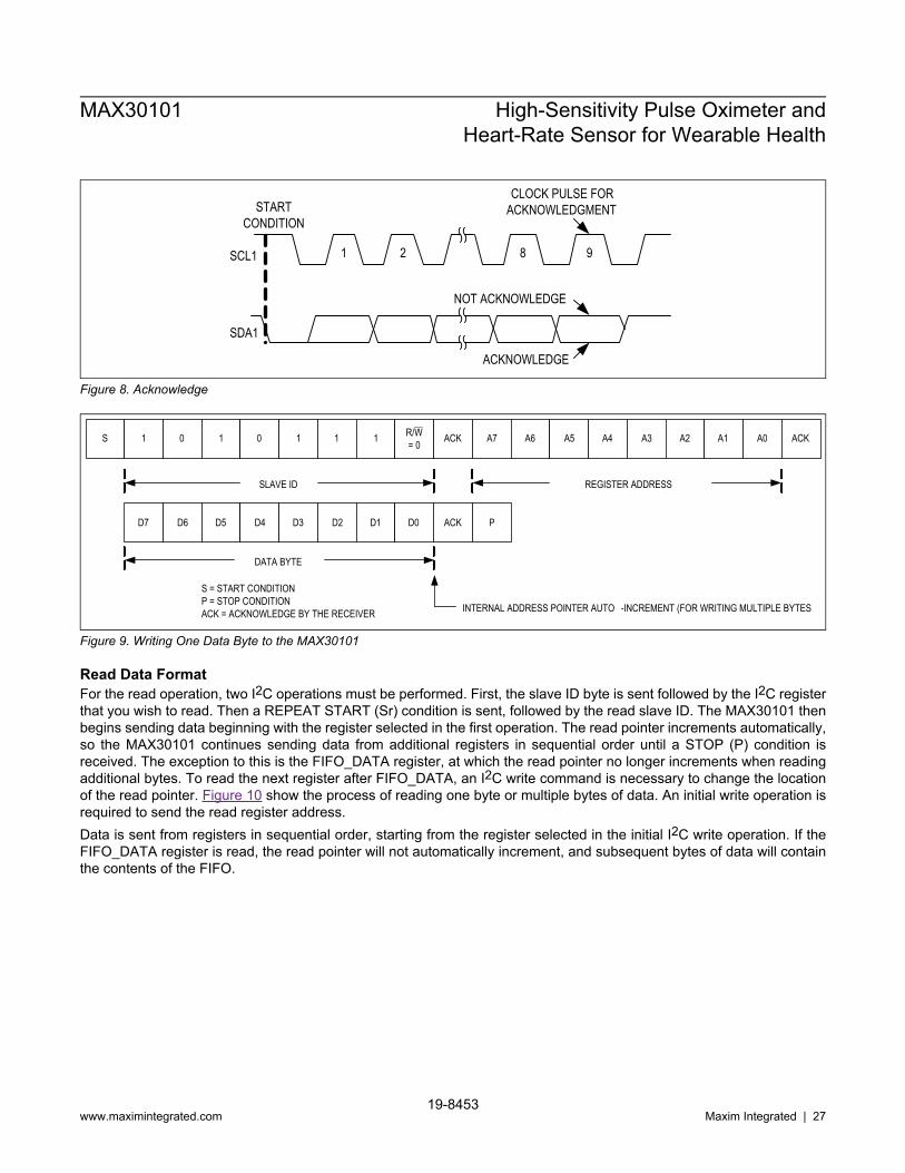
SCL1
SDA1
START CONDITION
1 2 8 9
CLOCK PULSE FORACKNOWLEDGMENT
NOT ACKNOWLEDGE
ACKNOWLEDGE
Figure 8. Acknowledge
S 1 0 1 0 1 1 1 R/W= 0 ACK A7 A6 A5 A4 A3 A2
SLAVE ID
A1 A0
ACK P
S = START CONDITIONP = STOP CONDITIONACK = ACKNOWLEDGE BY THE RECEIVER
REGISTER ADDRESS
D7 D6 D5 D4 D3 D2 D1 D0
ACK
DATA BYTE
INTERNAL ADDRESS POINTER AUTO -INCREMENT (FOR WRITING MULTIPLE BYTES
Figure 9. Writing One Data Byte to the MAX30101
Read Data FormatFor the read operation, two I2C operations must be performed. First, the slave ID byte is sent followed by the I2C registerthat you wish to read. Then a REPEAT START (Sr) condition is sent, followed by the read slave ID. The MAX30101 thenbegins sending data beginning with the register selected in the first operation. The read pointer increments automatically,so the MAX30101 continues sending data from additional registers in sequential order until a STOP (P) condition isreceived. The exception to this is the FIFO_DATA register, at which the read pointer no longer increments when readingadditional bytes. To read the next register after FIFO_DATA, an I2C write command is necessary to change the locationof the read pointer. Figure 10 show the process of reading one byte or multiple bytes of data. An initial write operation isrequired to send the read register address.Data is sent from registers in sequential order, starting from the register selected in the initial I2C write operation. If theFIFO_DATA register is read, the read pointer will not automatically increment, and subsequent bytes of data will containthe contents of the FIFO.
MAX30101 High-Sensitivity Pulse Oximeter andHeart-Rate Sensor for Wearable Health
www.maximintegrated.com19-8453
Maxim Integrated | 27

S 1 0 1 0 1 1 1 R/W= 0 ACK A7 A6 A5 A4 A3 A2 A1 A0 ACK
1 0 1 0 1 1 1 ACK D7 D6 D5 D4 D3 D2 D1 D0 NACK
DATA BYTE
P
S = START CONDITIONSr = REPEATED START CONDITIONP = STOP CONDITION
ACK = ACKNOWLEDGE BY THE RECEIVERNACK = NOT ACKNOWLEDGE
SLAVE ID REGISTER ADDRESS
Sr
SLAVE ID
R/W= 1
Figure 10. Reading one byte of data from MAX30101
S 1 0 1 0 1 1 1 R/W= 0 ACK A7 A6 A5 A4 A3 A2 A1 A0 ACK
1 0 1 0 1 1 1 ACK D7 D6 D5 D4 D3 D2 D1 D0 AM
DATA 1
S = START CONDITIONSr = REPEATED START CONDITIONP = STOP CONDITION
ACK = ACKNOWLEDGE BY THE RECEIVERAM = ACKNOWLEDGE BY THE MASTERNACK = NOT ACKNOWLEDGE
SLAVE ID REGISTER ADDRESS
Sr
SLAVE ID
R/W= 1
D7 D6 D5 D4 D3 D2 D1 AM D7 D6 D5 D4 D3 D2 D1 D0 NACK
DATA n
P
DATA n-1
D0
Figure 11. Reading multiple bytes of data from the MAX30101
MAX30101 High-Sensitivity Pulse Oximeter andHeart-Rate Sensor for Wearable Health
www.maximintegrated.com19-8453
Maxim Integrated | 28
Applications Information
Soldering and Cleaning RecommendationsThe MAX30101 comes in an OLGA package that is not sealed from dust or liquid. Because of this, the MAX30101requires special care to install on a board.If possible, the MAX30101 should be the last component installed on the board. Install the MAX30101 after theboard ultrasonic cleaning is completed. When soldering the MAX30101, use a low-residue, no-clean solder paste. TheMAX30101 should not be cleaned with a liquid solution, baked, or coated with anything.The Application Note 6381 serves as a guide for handling the OLGA package when manufacturing a board.
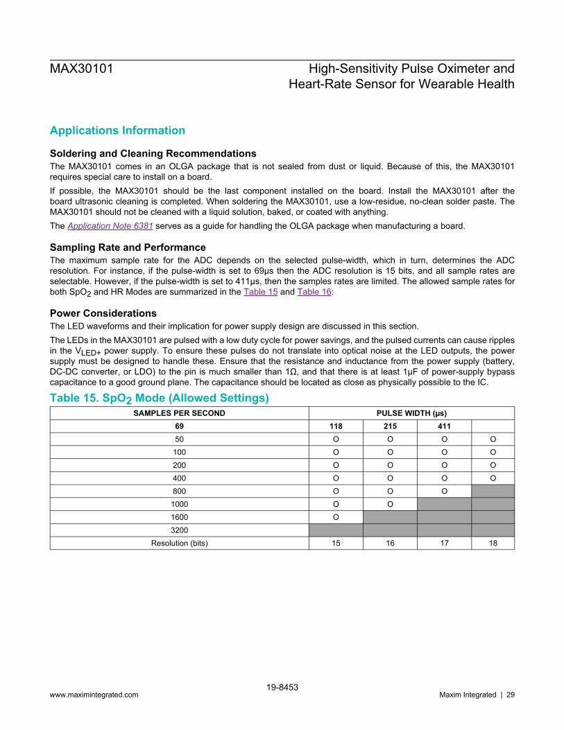
Sampling Rate and PerformanceThe maximum sample rate for the ADC depends on the selected pulse-width, which in turn, determines the ADCresolution. For instance, if the pulse-width is set to 69μs then the ADC resolution is 15 bits, and all sample rates areselectable. However, if the pulse-width is set to 411μs, then the samples rates are limited. The allowed sample rates forboth SpO2 and HR Modes are summarized in the Table 15 and Table 16:
Power ConsiderationsThe LED waveforms and their implication for power supply design are discussed in this section.The LEDs in the MAX30101 are pulsed with a low duty cycle for power savings, and the pulsed currents can cause ripplesin the VLED+ power supply. To ensure these pulses do not translate into optical noise at the LED outputs, the powersupply must be designed to handle these. Ensure that the resistance and inductance from the power supply (battery,DC-DC converter, or LDO) to the pin is much smaller than 1Ω, and that there is at least 1μF of power-supply bypasscapacitance to a good ground plane. The capacitance should be located as close as physically possible to the IC.
Table 15. SpO2 Mode (Allowed Settings)SAMPLES PER SECOND PULSE WIDTH (µs)
69 118 215 41150 O O O O
100 O O O O200 O O O O400 O O O O800 O O O
1000 O O1600 O3200
Resolution (bits) 15 16 17 18
MAX30101 High-Sensitivity Pulse Oximeter andHeart-Rate Sensor for Wearable Health
www.maximintegrated.com19-8453
Maxim Integrated | 29
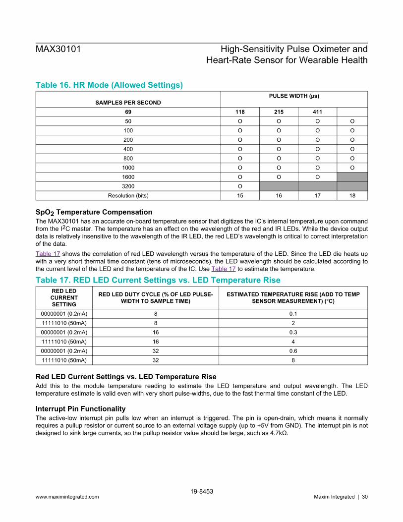
Table 16. HR Mode (Allowed Settings)
SAMPLES PER SECONDPULSE WIDTH (µs)
69 118 215 41150 O O O O
100 O O O O200 O O O O400 O O O O800 O O O O
1000 O O O O1600 O O O3200 O
Resolution (bits) 15 16 17 18
SpO2 Temperature CompensationThe MAX30101 has an accurate on-board temperature sensor that digitizes the IC’s internal temperature upon commandfrom the I2C master. The temperature has an effect on the wavelength of the red and IR LEDs. While the device outputdata is relatively insensitive to the wavelength of the IR LED, the red LED’s wavelength is critical to correct interpretationof the data.Table 17 shows the correlation of red LED wavelength versus the temperature of the LED. Since the LED die heats upwith a very short thermal time constant (tens of microseconds), the LED wavelength should be calculated according tothe current level of the LED and the temperature of the IC. Use Table 17 to estimate the temperature.
Table 17. RED LED Current Settings vs. LED Temperature RiseRED LEDCURRENTSETTING
RED LED DUTY CYCLE (% OF LED PULSE-WIDTH TO SAMPLE TIME)
ESTIMATED TEMPERATURE RISE (ADD TO TEMPSENSOR MEASUREMENT) (°C)
00000001 (0.2mA) 8 0.111111010 (50mA) 8 200000001 (0.2mA) 16 0.311111010 (50mA) 16 400000001 (0.2mA) 32 0.611111010 (50mA) 32 8
Red LED Current Settings vs. LED Temperature RiseAdd this to the module temperature reading to estimate the LED temperature and output wavelength. The LEDtemperature estimate is valid even with very short pulse-widths, due to the fast thermal time constant of the LED.
Interrupt Pin FunctionalityThe active-low interrupt pin pulls low when an interrupt is triggered. The pin is open-drain, which means it normallyrequires a pullup resistor or current source to an external voltage supply (up to +5V from GND). The interrupt pin is notdesigned to sink large currents, so the pullup resistor value should be large, such as 4.7kΩ.
MAX30101 High-Sensitivity Pulse Oximeter andHeart-Rate Sensor for Wearable Health
www.maximintegrated.com19-8453
Maxim Integrated | 30
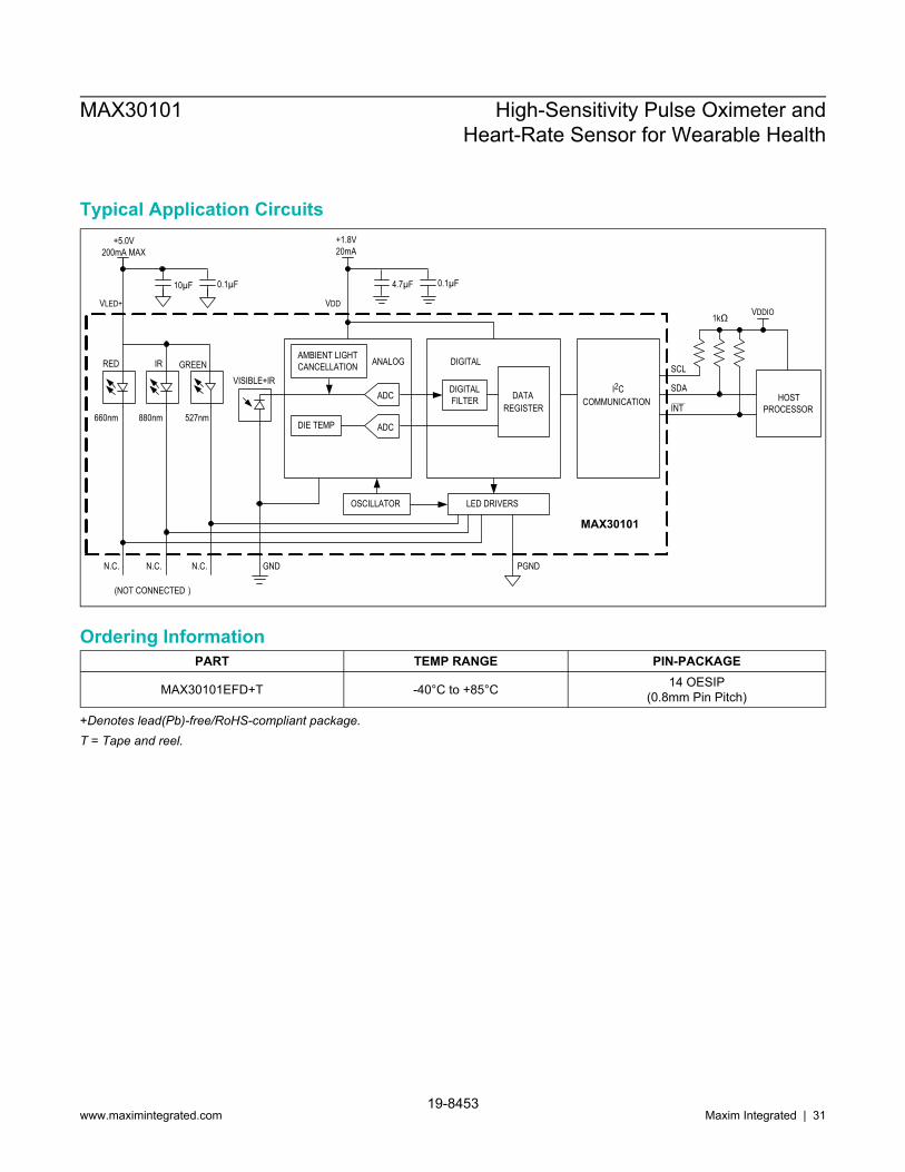
Typical Application Circuits
880nm660nm
ADC
AMBIENT LIGHT CANCELLATION ANALOG
ADCDIE TEMP
OSCILLATOR
DIGITAL FILTER
DIGITAL
DATAREGISTER
LED DRIVERS
I2CCOMMUNICATION INT
SDA
SCL
VDD
N.C.N.C. GND PGND
RED IR
VISIBLE+IR
1kΩ VDDIO
HOSTPROCESSOR
(NOT CONNECTED )
MAX30101
GREEN
527nm
N.C.
+5.0V200mA MAX
VLED+
10µF 0.1µF 4.7µF
+1.8V20mA
0.1µF
Ordering InformationPART TEMP RANGE PIN-PACKAGE
MAX30101EFD+T -40°C to +85°C 14 OESIP(0.8mm Pin Pitch)
+Denotes lead(Pb)-free/RoHS-compliant package.T = Tape and reel.
MAX30101 High-Sensitivity Pulse Oximeter andHeart-Rate Sensor for Wearable Health
www.maximintegrated.com19-8453
Maxim Integrated | 31

Revision HistoryREVISIONNUMBER
REVISIONDATE DESCRIPTION PAGES
CHANGED0 3/16 Initial release —
1 6/18 Changed register descriptions, updated tables 8,9,13,15,16, removed Proximityfunction, updated FIFO_A_FULL description table
10–15, 18,21–25, 27, 28
2 9/18
Updated the Applications, Absolute Maximum Ratings, Electrical Characteristics, PinDescription, and Power-Up Sequencing sections; updated the System Diagram, PinConfiguration, Functional Diagram, and Typical Application Circuit; updated theRegister Maps and Descriptions, Mode Configuration (0x09), SpO2 Configuration(0x0A), LED Pulse Amplitude (0x0C–0x0F), Table 8, and Table 9.
1–5, 9–11,19,21–22, 29, 32
3 6/20 Updated SpO2 Sample Rate Control[2:4] (0x0A) and Applications Informationsection 24, 34
For pricing, delivery, and ordering information, please visit Maxim Integrated’s online storefront at https://www.maximintegrated.com/en/storefront/storefront.html.
Maxim Integrated cannot assume responsibility for use of any circuitry other than circuitry entirely embodied in a Maxim Integrated product. No circuit patentlicenses are implied. Maxim Integrated reserves the right to change the circuitry and specifications without notice at any time. The parametric values (min and maxlimits) shown in the Electrical Characteristics table are guaranteed. Other parametric values quoted in this data sheet are provided for guidance.
MAX30101 High-Sensitivity Pulse Oximeter andHeart-Rate Sensor for Wearable Health
Maxim Integrated and the Maxim Integrated logo are trademarks of Maxim Integrated Products, Inc. © 2020 Maxim Integrated Products, Inc.

Mouser Electronics
Authorized Distributor
Click to View Pricing, Inventory, Delivery & Lifecycle Information: Maxim Integrated:
MAX30101EFD+ MAX30101EFD+T