clock tree embedding for 3d ics - asp-dac 1995clock tree embedding for 3d ics 15th asia and south...
TRANSCRIPT

Clock Tree Embedding for 3D ICs15th Asia and South Pacific Design Automation ConferenceTaipei, TaiwanJanuary 18-21, 2010
Tak-Yung Kim and Taewhan Kim
System Synthesis LaboratorySchool of Electrical Engineering and Computer ScienceSeoul National University

Contents 3-Dimensional Integrated Circuit Clock Tree Synthesis Clock Tree Embedding for 3D ICs
Zero Skew Clock Tree Embedding Minimization of the number of through-silicon vias Minimization of the total wirelength
Clock Tree Synthesis Flow for 3D ICs Experimental Results Conclusions
1

3-Dimensional Integrated Circuit Chip with multiple layers of active devices
by vertically stacking into a single chip or package. Currently, a true 3D IC design technology using
TSVs has been actively researched. Advantages & Issues
2
Advantages Issues Short global interconnection wire
Performance/Power/Area benefit Small form factor
System size reduction Heterogeneous technology integration
Manufacturing cost Yield Thermal problem Noise problem Physical design automation

3D Physical Design Automation Various algorithms have been researched in
the area of floorplanning, placement, and routing.
Clock tree synthesis for 3D ICs Minz, Zhao, and Lim developed a thermal-aware
buffered clock tree synthesis solution.(BURITO; ASPDAC2008) Minimizes and balances the temperature dependent skew. Limited to two layered face-to-face wafer bonded 3D ICs. Does not effectively consider the clock tree embedding
problem in a vertical design space.
3

Clock Tree Synthesis
4
s1
s2
s4
s3
x1
x2
s0
Embedding
2. Embedding (Routing) 3. Buffering
CTS algorithm should consider3-dimensional design space !!!
- Vertical die layers- Through-silicon viass2 s4
Clock root s0
Sinks s3s1
1. Topology Generation
s2 s4s3
x1 x2
s0
s1
s1
s2
s4
s3
x1
x2
s0

Minimizing the weighted sumof TSVs and wirelength.
∑⋅+⋅∀x
xs ewTnvw ||)( 21 0
Zero Skew Clock Tree Embedding
5
s1
s2
s4
s3
x1
x2
s0
Embeddings2 s4s3
x1 x2
s0
s1
• A set S of sink locations• A tree topology G(S)
Construct a zero skew clock tree embedding T(S)
w1, w2: weighting factorsnv(Tx): the number of TSVs in the clock tree Tx|ex|: edge length from the parent node

Proposed Algorithm
6
ZCTE-3D(Zero Skew Clock Tree Embedding in 3D ICs)
Solves the problem for a given topology in two steps.
Subproblem 1
TSV allocation problem
Minimize the number of TSVs
Subproblem 2
3D clock tree embedding problem with TSV placement
Minimize the total wirelength
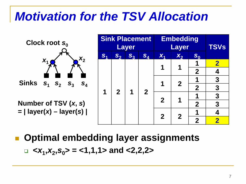
Motivation for the TSV Allocation
Optimal embedding layer assignments <x1,x2,s0> = <1,1,1> and <2,2,2>
7
Sink PlacementLayer
EmbeddingLayer TSVs
s1 s2 s3 s4 x1 x2 s0
1 2 1 2
1 1 1 22 4
1 2 1 32 3
2 1 1 32 3
2 2 1 42 2
s2 s4
Clock root s0
Sinks s3
x1x2
s1
Number of TSV (x, s)= | layer(x) – layer(s) |

Number of TSVs & Embedding Layers The number of TSVs is computed by
TSVs allocated in the sub-trees rooted at children TSVs needed for routing to children.
8
+++=
node. internalan is if )),(,())(,()()(node.sink leaf a is if ,0
)()()( xxrightxnvxleftxnvTnvTnv
xTnv
xrightxleftx
left(x)
x
right(x)
TSVs of the sub-treesTSVs for routing to children
The number of TSVs is decidedby the embedding layers of tree nodes.

Embedding Layer Assignment
9
left(x)
x
right(x)
1st Bottom-up PhaseConstructembedding layer candidates.
2nd Top-down PhaseAssignthe exact embedding layer.

Embedding Layer Candidates
Find embedding layer candidates el(x) = <l1,l2>.
Node x can be assigned to a layer between l1 and l2.
10
s1<1,1>
s2<2,2>
s3<2,2>
s4<3,3>
x1<?,?>
x2<?,?>
s0<?,?>
s1<1,1>
s2<2,2>
s3<2,2>
s4<3,3>
x1<1,2>
x2<2,3>
s0<?,?>
s1<1,1>
s2<2,2>
s3<2,2>
s4<3,3>
x1<1,2>
x2<2,3>
s0<2,2>

Exact Embedding Layer Assignment
11
s1<1,1>
s2<2,2>
s3<2,2>
s4<3,3>
x1<1,2>
x2<2,3>
s0<2,2>
Root node: assign any layer in el(s0). Other nodes: assign the nearest layer
in el(x) to the parent node.
s1<1,1>
s2<2,2>
s3<2,2>
s4<3,3>
x1<1,2>
x2<2,3>
s0<2,2>
Number of TSVs = 2
s1<1,1>
s2<2,2>
s3<2,2>
s4<3,3>
x1<2,2>
x2<2,2>
s0<2,2>
TSV TSV

Optimality of Embedding Layer Assignment
12
Lemma 1: Optimality of embedding layer candidates el(⋅)
Embedding layer candidates el(⋅) contain an assignment of embedding layers of optimal TSV allocation.
Lemma 2: Optimality of nearest embedding layer assignment
The nearest embedding layer assignment in el(⋅) leads to an optimal TSV allocation.
1st Bottom-up PhaseEmbedding layer candidates construction
2nd Top-down PhaseThe exact embedding layer assignment

Minimization of the Total Wirelength Find the precise (x,y)-location with TSV placement.
Extended the 2D clock tree embedding algorithm DME (Deferred Merge Embedding) (Chao et al., TCAS1992) Wirelength optimal under the linear delay model Suboptimal under the Elmore delay model
For a prescribed clock connection topology 1st bottom-up phase: Constructs a tree of merging segments,
which represent loci of possible placements of tree nodes. 2nd top-down phase: Decide the exact embedding locations of
tree nodes.
13

DME on 3D Design Space Construction of merging segment ms(v),
with TRR (Tilted Rectangular Region)
Edge length |ex| calculation is modified to consider the delays of TSVs as well as 2D wires.
The (x,y)-location of TSVs is also concurrently decided based on the parasitic values of TSV and interconnect wire.
14
|eb|
trra=ms(a) ms(b)
ms(v)
trrb
ms(b)ms(a)
ms(v)
|eb|
|ea|
trrbtrrav
a b
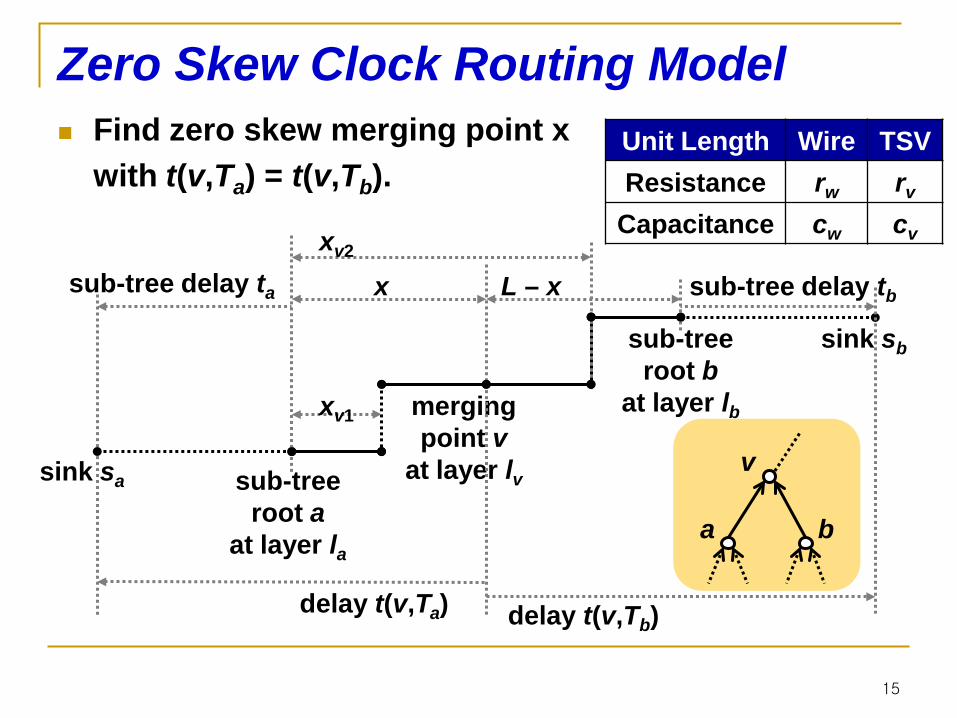
Zero Skew Clock Routing Model Find zero skew merging point x
with t(v,Ta) = t(v,Tb).
15
sink sa
sink sbsub-tree root b
at layer lb
sub-tree root a
at layer la
merging point v
at layer lv
x L – x
delay t(v,Tb)delay t(v,Ta)
sub-tree delay ta sub-tree delay tb
xv2
xv1
Unit Length Wire TSVResistance rw rv
Capacitance cw cv
v
a b
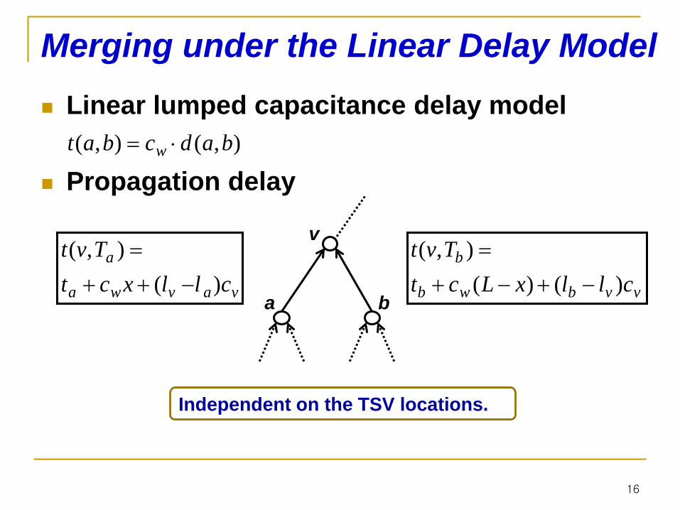
Merging under the Linear Delay Model Linear lumped capacitance delay model
Propagation delay
16
vavwa
a
cllxctTvt
)(),(
−++=
Independent on the TSV locations.
v
a b
),(),( badcbat w ⋅=
vvbwb
b
cllxLctTvt
)()(),(
−+−+=

Merging under the Linear Delay Model Edge length calculation
|ea|=x and |eb|=L–x (0≤x≤L)
17
w
vvbawab
cclllLcttx
2)2()( −+++−
=
– cont’
v
a b
ms(v)
a
b
( la = lb = lv )
a ms(v)
b
TSV
( la = 1, lb = 2, lv = 1 )
ms(v)
b
TSV
( la = 1, lb = 2, lv = 2 )
a
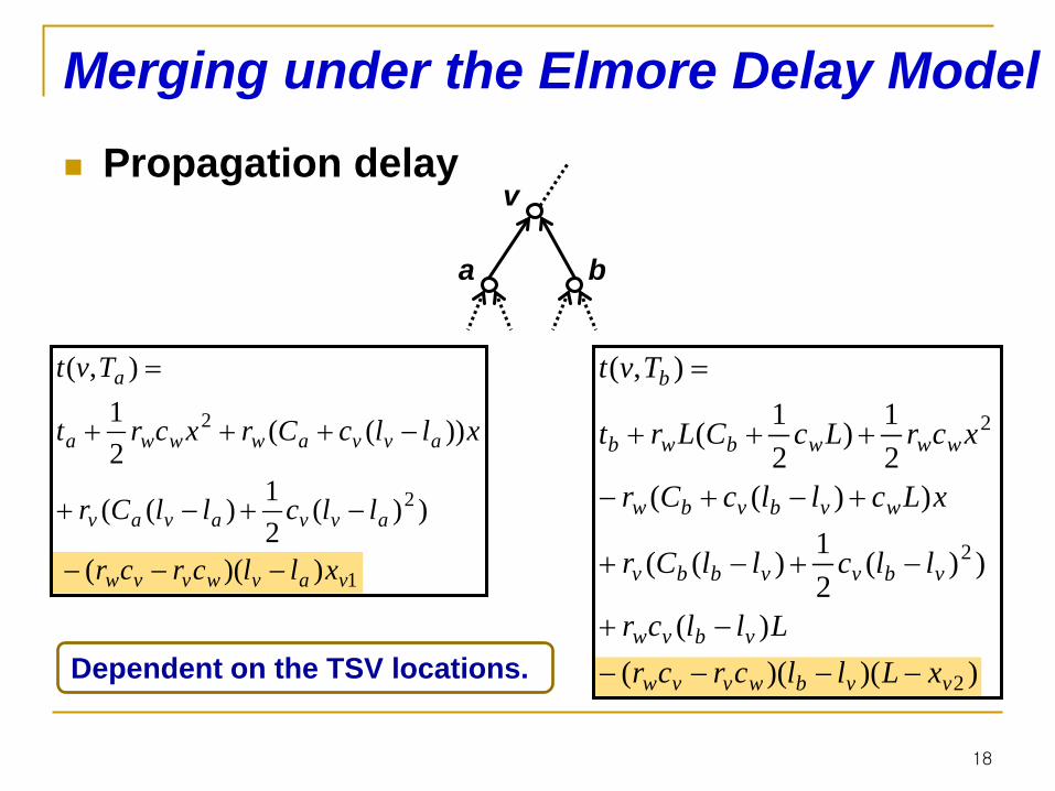
Merging under the Elmore Delay Model Propagation delay
18
1
2
2
))((
))(21)((
))((21
),(
vavwvvw
avvavav
avvawwwa
a
xllcrcr
llcllCr
xllcCrxcrt
Tvt
−−−
−+−+
−+++
=
))()(()(
))(21)((
))((21)
21(
),(
2
2
2
vvbwvvw
vbvw
vbvvbbv
wvbvbw
wwwbwb
b
xLllcrcrLllcr
llcllCr
xLcllcCr
xcrLcCLrt
Tvt
−−−−−+
−+−+
+−+−
+++
=
Dependent on the TSV locations.
v
a b

Merging under the Elmore Delay Model Edge length calculation
|ea|=x and |eb|=L–x (0≤x≤L)
19
)))()((21)()((
,0,0)( ,)()(
)()21()(
,0)( ,)()(
)()21()(
22
21
21
avvbvaavbvbv
vvwvvwabvwwbaw
vbvwwbwab
vvwvvwabwvwbaw
vbwvwbwab
llllcCllCllr
LxxcrcrllcrLcCCr
LllcrLcCLrtt
xxxcrcrllcrLcCCr
LllcrLcCLrtt
x
−−−+−−−=
==<−−+++
−++++−
==≥−−+++
−++++−
=
β
β
β
TSVs are on the merging location.
TSVs are on the location of children
– cont’

ZCTE-3D
Zero SkewClock TreeEmbeddingin 3D ICs
Proposed 3D Clock Tree Synthesis Flow
20
Tree Topology Generation( MMM-3D )
Embedding Layer Assignmentfor Optimal TSV Allocation
( Assign-Embedding-Layer )
Clock Tree Embeddingwith TSV Placement
( DME-3D )
Synthesized Clock Tree for 3D ICs

Tree Topology Generation for 3D ICs (MMM-3D) Extended MMM (Method of Means and Medians) (Jackson et al.,
DAC1990): Recursively divides sinks based on the (x,y)-coordinates. If HPWL(subset) ≤ ρ⋅L (0≤ρ≤1, L = HPWL(all sinks)),
Partitions the sinks according to the placement layers. Controls the density of TSVs
21
s1 s2 s3 s4s1 s3 s2 s4ρ=0
s1
s3
s4
1st cut
s2
ρ=1
s1
s2
s3
s4
1st cut
2nd cut
Layer-1
Layer-2

Experimental Results 2-Layered 3D ICs under Elmore delay model Total number of TSVs: 10% ↓ Total wirelength: 4% ↓ Max clock network delay: 2% ↓
22
benchmarkALL_BURITO (100%) BURITO + ZCTE-3D MMM-3D + ZCTE-3D
TSVs WL(um)
Delay(ns) TSVs WL
(um)Delay(ns) TSVs WL
(um)Delay(ns)
r1 88 1496266 1.68 82 1496538 1.67 83 1441849 1.64r2 225 2994996 4.34 197 2996950 4.29 197 2831346 4.34r3 309 3869936 6.75 283 3872996 6.71 276 3725294 6.37r4 725 7784107 19.82 658 7789465 19.68 653 7424886 19.28r5 1161 11385430 35.75 1033 11393346 35.54 1052 10940984 35.2
ratio 1 1 1 0.9 1 0.99 0.9 0.96 0.98
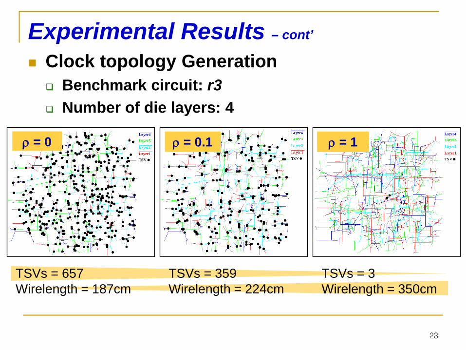
Experimental Results – cont’
Clock topology Generation Benchmark circuit: r3 Number of die layers: 4
23
ρ = 0
TSVs = 657Wirelength = 187cm
ρ = 0.1
TSVs = 359Wirelength = 224cm
ρ = 1
TSVs = 3Wirelength = 350cm

Conclusions The zero skew clock tree embedding algorithm ZCTE-3D
is proposed. Allocates optimal number of TSVs. (Assign-Embedding-Layer) Minimizes the total wirelength by extending 2D DME algorithm to
3D design space. (DME-3D) Wirelength optimal under the linear delay model. Suboptimal under the Elmore delay model.
3D topology generation algorithm MMM-3D is proposed.
24

Thank You !!!