comparison between i g integration and v gs derivation
TRANSCRIPT
HAL Id: hal-02972905https://hal.archives-ouvertes.fr/hal-02972905
Submitted on 20 Oct 2020
HAL is a multi-disciplinary open accessarchive for the deposit and dissemination of sci-entific research documents, whether they are pub-lished or not. The documents may come fromteaching and research institutions in France orabroad, or from public or private research centers.
L’archive ouverte pluridisciplinaire HAL, estdestinée au dépôt et à la diffusion de documentsscientifiques de niveau recherche, publiés ou non,émanant des établissements d’enseignement et derecherche français ou étrangers, des laboratoirespublics ou privés.
Comparison between i g integration and v gs derivationmethods dedicated to fast short-circuit 2D diagnosis for
wide bandgap power transistorsYazan Barazi, Nicolas Rouger, Frédéric Richardeau
To cite this version:Yazan Barazi, Nicolas Rouger, Frédéric Richardeau. Comparison between i g integration and v gsderivation methods dedicated to fast short-circuit 2D diagnosis for wide bandgap power transistors.Mathematics and Computers in Simulation, Elsevier, 2020, 10.1016/j.matcom.2020.05.011. hal-02972905

1
Comparison Between ig Integration and vgs Derivation Methods
Dedicated to Fast Short-Circuit 2D Diagnosis for Wide Bandgap
Power Transistors
Yazan Barazi, Nicolas Rouger, Frédéric Richardeau
LAPLACE, University of Toulouse, CNRS, Toulouse, France
E-mail: [email protected]; [email protected]; [email protected]
2 rue Charles Camichel Toulouse, BP7122 – 31071 Toulouse Cedex 07, France
Abstract This study presents and compares two original high-speed protection circuit methods, namely, ig
integration and vgs derivation, against short-circuit types, referred to as, the hard switch fault and fault under
load. Since the gate-drain capacitor Cgd of a power device depends on the drain to source voltage vds, it can
become an original native sensor to monitor the switching operation and so detect the unwanted vds transition or
the absence of the vds transition by monitoring only vgs. The use of only low-voltage monitoring, such as vgs, is an
essential step to integrate fast and embedded new detection methods into a low-voltage application-specific
integrated circuit gate driver, in particular for wide bandgap power transistors. The Cgd capacitor plays a major
part in the two detection methods. The first method is based on dedicated two-dimensional monitoring of the
gate charge transferred in a time interval combined with gate voltage monitoring. The second method consists of
the reconstruction of the dvgs/dt by means of a capacitive current sensing to provide the vgs derivation combined
with the vgs monitoring. Comparison and simulation of the methods based on a C2M0025120D SiC MOSFET
device under LTspice™ are made to verify the validity of the methods. In terms of detection speed of the short
circuit, a detection time of 200 ns is obtained for both methods. Experimental waveforms based on
C3M0120090J SiC MOSFET device were included into LTspiceTM
to push furthermore the methods to their
limits and validate the approaches. Both methods are easy to design and to integrate. However, the robustness
and the speed of detection trade-off of all these methods should be analysed and compared relative to the critical
functionalities.
Keywords: Silicon carbide MOSFETs; normal turn on; short circuit; hard switch fault; fault under load; gate
charge
2
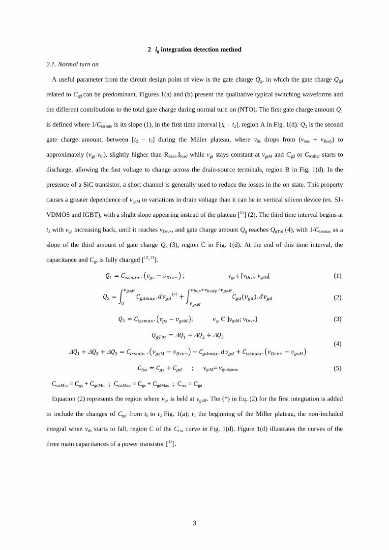
1 Introduction
Wide bandgap semiconductor materials, such as silicon carbide (SiC), have undergone a tremendous
evolution in recent years. Power semiconductor devices, such as insulted gate bipolar transistors (IGBTs) and
super-junction (SJ-MOSFET) silicon devices, are limited in terms of maximum switching speeds. Consequently,
silicon power devices have high switching losses and large and expensive thermal management systems. In
contrast, SiC MOSFETs are promising power semiconductor devices for high density converters, with low
conduction and switching losses and high temperature stability [1]. However, today, the short-circuit (SC) delay
time capability for SiC MOSFETs is lower than for silicon devices [2]. Power converters designed with these
components are therefore less robust.
Power semiconductors devices are used in various industrial applications, including motor drives, battery
chargers, switch mode power supplies and converters. These devices are exposed to several types of SC. The
hard switch fault (HSF, SC type I) and fault under load (FUL, SC type II) are the two main fault behaviours.
Safety is necessary for these typical applications. Several ways of protecting circuits have been presented for
either silicon IGBTs or MOSFETs [3]. Most of the previously proposed techniques rely on the drain-source
voltage or current. This is clearly a limiting approach due to the high voltage detection diode or additional
current sensor used, such as MOSFET-sense-current in non-standard dies [4-5-6-7
].
In SiC MOSFETs, the drain current ids is controlled by the gate voltage vgs. Since most wide bandgap (WBG)
power FETs exhibit a low robustness and a typical fail-to-short behaviour [8-9-10
], they must be turned-off softly
within a few hundreds of nanoseconds after fault detection. Good management of the gate voltage results in the
best compromise between losses in electromagnetic induction safety. The reverse transfer capacitance “Crss =
Cgd” of a SiC MOSFET, also known as the Miller capacitance, is one of the most important parameters in
switching performances for unipolar devices. This capacitance is a nonlinear function of voltages vgs and vds and
it provides a feedback between the output voltage vds and the input vgs of the device.
In this article, detailed analyses and comparisons between the SC detection methods are presented. LTspice™
simulated results are presented in view of verifying the SC detection methods to further protect SiC MOSFETs.
3
2 ig integration detection method
2.1. Normal turn on
A useful parameter from the circuit design point of view is the gate charge Qg, in which the gate charge Qgd
related to Cgd can be predominant. Figures 1(a) and (b) present the qualitative typical switching waveforms and
the different contributions to the total gate charge during normal turn on (NTO). The first gate charge amount Q1
is defined where 1/Cissmin is its slope (1), in the first time interval [t0 – t2], region A in Fig. 1(d). Q2 is the second
gate charge amount, between [t2 – t3] during the Miller plateau, where vds drops from (vbus + vBody) to
approximately (vgs-vth), slightly higher than Rdson.Iload while vgs stays constant at vgsM and Cgd or CMiller starts to
discharge, allowing the fast voltage to change across the drain-source terminals, region B in Fig. 1(d). In the
presence of a SiC transistor, a short channel is generally used to reduce the losses in the on state. This property
causes a greater dependence of vgsM to variations in drain voltage than it can be in vertical silicon device (ex. SJ-
VDMOS and IGBT), with a slight slope appearing instead of the plateau [11
] (2). The third time interval begins at
t3 with vgs increasing back, until it reaches vDrv+, and gate charge amount Qg reaches QgTot (4), with 1/Cissmax as a
slope of the third amount of gate charge Q3 (3), region C in Fig. 1(d). At the end of this time interval, the
capacitance and Cgs is fully charged [12_13
].
; vgs є [vDrv-; vgsM[ (1)
(2)
; vgs Є ]vgsM; vDrv+] (3)
(4)
; vgsM= vgsplateau (5)
CissMin = Cgs + CgdMin ; CissMax = Cgs + CgdMax ; Crss = Cgd
Equation (2) represents the region where vgs is held at vgsM. The (*) in Eq. (2) for the first integration is added
to include the changes of Cgd from t0 to t2 Fig. 1(a); t2 the beginning of the Miller plateau, the non-included
integral when vds starts to fall, region C of the Crss curve in Fig. 1(d). Figure 1(d) illustrates the curves of the
three main capacitances of a power transistor [14
].

4
Fig. 1. (a) Turn-on switching characteristics of SiC MOSFET under NTO conditions. (b) Gate charge
characteristics “NTO”. (c) Equivalent circuit of the half bridge. (d) Capacitance variation.
*Note (Figs. 1–3): For the purposes of a simple graphical representation, Cgs and Cgd capacitors are taken here
as constant values, except Cgd, which is modelled as its two asymptotic values CgdMin and CgdMax as illustrated in
Fig.1 (d). The voltage drops in the on state of the components (diode and transistor) are also not taken into
account for the switching study. A constant Miller plateau is also assumed in the figures. Neither the reverse
recovery nor the parasitic inductances are taken into account, here, but will be discussed throughout this article
in taken into consideration later on the chapters.
2.2. Hard switch fault
Contrary to fault condition type I, when vgs = vgsM at t2, vgs and ids continue to increase until vgs reaches vDrv+ and
ids overcurrent, t3, ids = isat-channel. vds stays at the vbus value, which causes the transistor to operate in its saturation
regime, as shown in Fig. 2(a). Such a regime can be sustainable only for a couple of µs, as presented in [10
]. The
amount of gate charge is QSC-HSF with a 1/Cissmin slope, exhibiting no change in the charging rate of the input
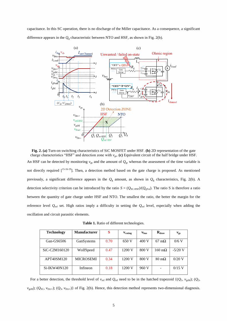
5
capacitance. In this SC operation, there is no discharge of the Miller capacitance. As a consequence, a significant
difference appears in the Qg characteristic between NTO and HSF, as shown in Fig. 2(b).
Fig. 2. (a) Turn-on switching characteristics of SiC MOSFET under HSF. (b) 2D representation of the gate
charge characteristics “HSF” and detection zone with vgs. (c) Equivalent circuit of the half bridge under HSF.
An HSF can be detected by monitoring vgs and the amount of Qg, whereas the assessment of the time variable is
not directly required [15-16-19
]. Then, a detection method based on the gate charge is proposed. As mentioned
previously, a significant difference appears in the Qg amount, as shown in Qg characteristics, Fig. 2(b). A
detection selectivity criterion can be introduced by the ratio S = (QSC-HSF)/(QgTot). The ratio S is therefore a ratio
between the quantity of gate charge under HSF and NTO. The smallest the ratio, the better the margin for the
reference level Qref set. High ratios imply a difficulty in setting the Qref level, especially when adding the
oscillation and circuit parasitic elements.
Table 1. Ratio of different technologies.
Technology Manufacturer S vrating vbus Rdson vgs
Gan-GS6506 GanSystems 0.70 650 V 400 V 67 mΩ 0/6 V
SiC-C2M160120 WolfSpeed 0.47 1200 V 800 V 160 mΩ -5/20 V
APT40SM120 MICROSEMI 0.34 1200 V 800 V 80 mΩ 0/20 V
Si-IKW40N120 Infineon 0.18 1200 V 960 V - 0/15 V
For a better detection, the threshold level of vref and Qref need to be in the hatched trapezoid (Q1, vgsM); (Q2,
vgsM); (QSC, vDrv+); (Q3, vDrv+) of Fig. 2(b). Hence, this detection method represents two-dimensional diagnosis.
6
Most of the time, this Qg characteristic figure is given in the datasheet under NTO. The choice of the threshold
detection levels vref and Qref can then be assessed from the datasheet. The method is naturally robust against
variation in switching delay time due to variation in threshold voltage or current operating point of the load.
With a constant threshold level, the detection will simply be a matter of integrated block design to obtain the
gate charge Qg [15-16
].
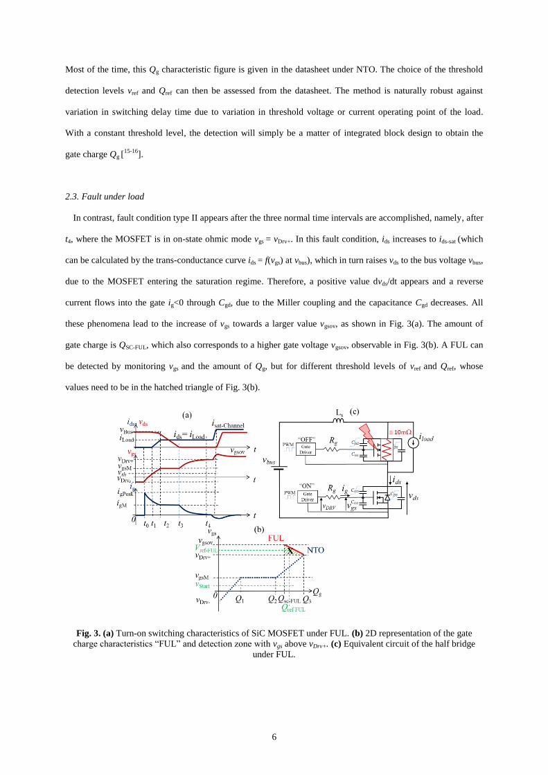
2.3. Fault under load
In contrast, fault condition type II appears after the three normal time intervals are accomplished, namely, after
t4, where the MOSFET is in on-state ohmic mode vgs = vDrv+. In this fault condition, ids increases to ids-sat (which
can be calculated by the trans-conductance curve ids = f(vgs) at vbus), which in turn raises vds to the bus voltage vbus,
due to the MOSFET entering the saturation regime. Therefore, a positive value dvds/dt appears and a reverse
current flows into the gate ig<0 through Cgd, due to the Miller coupling and the capacitance Cgd decreases. All
these phenomena lead to the increase of vgs towards a larger value vgsov, as shown in Fig. 3(a). The amount of
gate charge is QSC-FUL, which also corresponds to a higher gate voltage vgsov, observable in Fig. 3(b). A FUL can
be detected by monitoring vgs and the amount of Qg, but for different threshold levels of vref and Qref, whose
values need to be in the hatched triangle of Fig. 3(b).
Fig. 3. (a) Turn-on switching characteristics of SiC MOSFET under FUL. (b) 2D representation of the gate
charge characteristics “FUL” and detection zone with vgs above vDrv+. (c) Equivalent circuit of the half bridge
under FUL.
7
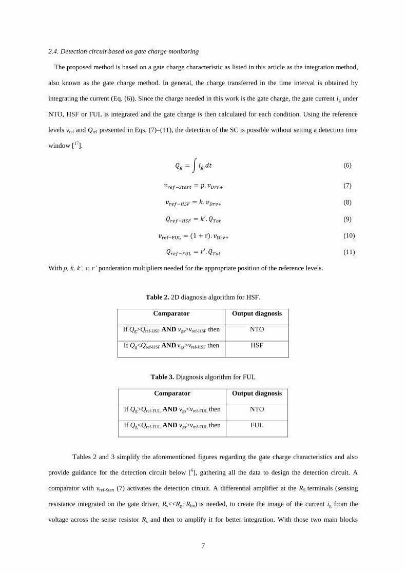
2.4. Detection circuit based on gate charge monitoring
The proposed method is based on a gate charge characteristic as listed in this article as the integration method,
also known as the gate charge method. In general, the charge transferred in the time interval is obtained by
integrating the current (Eq. (6)). Since the charge needed in this work is the gate charge, the gate current ig under
NTO, HSF or FUL is integrated and the gate charge is then calculated for each condition. Using the reference
levels vref and Qref presented in Eqs. (7)–(11), the detection of the SC is possible without setting a detection time
window [17
].
(6)
(7)
(8)
(9)
(10)
(11)
With p, k, k’, r, r’ ponderation multipliers needed for the appropriate position of the reference levels.
Table 2. 2D diagnosis algorithm for HSF.
Comparator Output diagnosis
If Qg>Qref-HSF AND vgs>vref-HSF then NTO
If Qg<Qref-HSF AND vgs>vref-HSF then HSF
Table 3. Diagnosis algorithm for FUL
Comparator Output diagnosis
If Qg>Qref-FUL AND vgs<vref-FUL then NTO
If Qg<Qref-FUL AND vgs>vref-FUL then FUL
Tables 2 and 3 simplify the aforementioned figures regarding the gate charge characteristics and also
provide guidance for the detection circuit below [6], gathering all the data to design the detection circuit. A
comparator with vref-Start (7) activates the detection circuit. A differential amplifier at the RS terminals (sensing
resistance integrated on the gate driver, Rs<<Rg+Rint) is needed, to create the image of the current ig from the
voltage across the sense resistor Rs and then to amplify it for better integration. With those two main blocks

8
(Diff. Amp. followed by Integrator), one obtains the gate charge Qg, which is then further compared with the
threshold Qref-HSF and Qref-FUL levels. Before that, to ensure that the detection is at the right moment, two
additional comparators with vref-HSF and vref-FUL are used to activate the monitoring, as shown in Fig. 4.
For HSF in Table 2, when the output of the vref-HSF comparator reaches a logic state ‘1’ (non-priority
value of the AND gate), this signal goes through the first input of the AND-HSF gate. The second input decides
the state of the detection circuit: if the calculated Qg is below the Qref-HSF, then the second input (the output of the
Qref-HSF) of the AND-HSF gate goes to the high ‘1’ logic state. The output of the AND-HSF gate goes high as
well, which generates a flag for further SC protection. In contrast, if one of those two inputs; the two outputs of
the vref-HSF and Qref-HSF comparators; is in a ‘0’ logic state, there is no flag and no detected SC. For FUL, the same
method is applied where both vref-FUL and Qref-FUL comparator outputs need to have a ‘1’ logic state.
Fig. 4. Fast 2D diagnosis and protection circuit based on gate charge.
Note: Rs = 1 Ω, R1 = R2 = 20 kΩ and other blocks are considered ideals.
This principle will be more sensitive and robust for lower QSC-HSF/QgTot ratios. This constraint is far from
assured for WBG devices, where the Cgd/Cgs ratio is voluntarily minimised by designers to reduce the cross-talk
phenomenon in inverter leg operation. As shown in Table 1, some commercially available SiC devices will be
more suitable than others. Commercially available high-voltage GaN power transistors seem poorly adapted to
this technique, while other protection techniques are adapted for GaN [18
]. Higher vref-HSF values lead to a more
robust diagnosis, albeit with longer delay times. Nevertheless, it remains a general principle, also named "2D
adaptive detection", only combining two low-voltage waveforms or signals without resorting directly to time
measurements. Another 2D SC detection method is based on the source sensing [19
]. One can note that our

9
proposed method can be easily integrated in a low voltage ASIC, which would not be allowed with classical
high-voltage detection Vdssat (saturation voltage) or would require high-voltage ASIC technology. Moreover, the
Qg method is an integral technique that will introduce less signal-to-noise ratio (SNR).
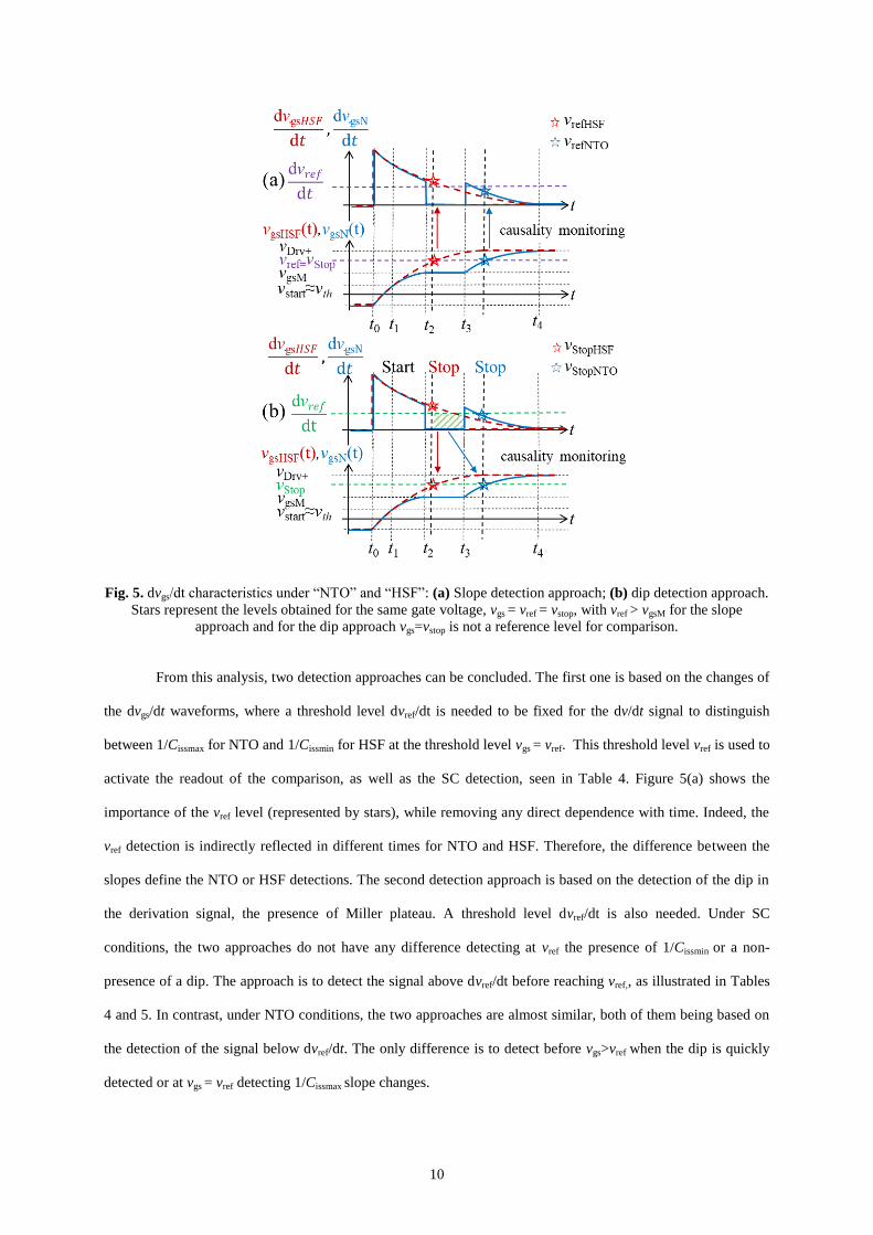
3 Derivation detection method
3.1. Behaviour and characteristics
Even with optimised detection thresholds, the previous method based on the gate-current integration over the
gate-voltage range may not be fast enough for SC protection. The following methods provide more direct quasi-
instantaneous detection without the need for the gate charge method. The impact of the capacitance Cgd on the
switching behaviour is also demonstrated for a new detection method based on monitoring the quasi-derivation
of vgs. There are three important time intervals on the behaviour of vgs, as explained above. The first one has a
slope of 1/Cissmin, followed by the Miller plateau, where Cgd is involved, and the last one has a slope of 1/Cissmax.
Using this alteration of slopes, a significant impact appears on their time derivatives. Figure 5 shows the dvgs/dt
signal behaviour under NTO and SC conditions, where two distinctive changes of slope can be observed. The
time interval [t0, t2] in Fig. 5 dvgs/dt signal presents a high peak “1/Cissmin>1/Cissmax”, followed by a decrease until
reaching a dip presenting the plateau period [t2, t3]. A smaller peak occurs at t3 to present 1/Cissmax. The dvgs/dt
signal under SC is reasonably straight forward, where there is only 1/Cissmin as a slope for vgs signal, from t0 to t4
dvgs/dt is the derivation of the slope 1/Cissmin, the dip or the smaller peak is not present. Figures 5(a) and (b)
introduce two different ways to analyse the derivation signal. Other approaches are studied on the detection of
the plateau [20
].
10
Fig. 5. dvgs/dt characteristics under “NTO” and “HSF”: (a) Slope detection approach; (b) dip detection approach.
Stars represent the levels obtained for the same gate voltage, vgs = vref = vstop, with vref > vgsM for the slope
approach and for the dip approach vgs=vstop is not a reference level for comparison.
From this analysis, two detection approaches can be concluded. The first one is based on the changes of
the dvgs/dt waveforms, where a threshold level dvref/dt is needed to be fixed for the dv/dt signal to distinguish
between 1/Cissmax for NTO and 1/Cissmin for HSF at the threshold level vgs = vref. This threshold level vref is used to
activate the readout of the comparison, as well as the SC detection, seen in Table 4. Figure 5(a) shows the
importance of the vref level (represented by stars), while removing any direct dependence with time. Indeed, the
vref detection is indirectly reflected in different times for NTO and HSF. Therefore, the difference between the
slopes define the NTO or HSF detections. The second detection approach is based on the detection of the dip in
the derivation signal, the presence of Miller plateau. A threshold level dvref/dt is also needed. Under SC
conditions, the two approaches do not have any difference detecting at vref the presence of 1/Cissmin or a non-
presence of a dip. The approach is to detect the signal above dvref/dt before reaching vref,, as illustrated in Tables
4 and 5. In contrast, under NTO conditions, the two approaches are almost similar, both of them being based on
the detection of the signal below dvref/dt. The only difference is to detect before vgs>vref when the dip is quickly
detected or at vgs = vref detecting 1/Cissmax slope changes.

11
Table 4. 2D diagnosis for HSF with vgs slope approach.
Comparator Output diagnosis
If vgs = vref AND dvgs/dt<dvref /dt
then
NTO
If vgs = vref AND dvgs/dt>dvref /dt
then
HSF
Table 5. 2D diagnosis for HSF with dip approach.
Comparator Output diagnosis
If dvgs/dt<dvref /dt AND vgs<vref then NTO
If dvgs/dt>dvref/dt AND vgs<vref then HSF
Both approaches can be accurate and robust because they are based on 2D detection dvgs/dt iCiss
combined with vgs. The second approach may be faster in NTO operation, where dip detection is before reaching
vref.
More importantly, the second approach (dip approach) should present a higher SNR than the slope
method thanks to the high signal amplitude detection.
This one, dip approach, may help the robustness of the detection by allowing a lower dvref/dt;
consequently, a wider discrimination range for a SC detection is offered, avoiding the small critical zone
whenever vgsNTO and vgsSC have similar values. The different threshold voltages must be defined from key
parameters extracted from the datasheet, operating conditions and experimental results.
3.2. Detection circuit based on derivation monitoring and simulation behaviour
The proposed method is based on the derivation method. As known, the current that runs through a capacitor is
given by the voltage/current relationship (12), where Cs is the sensing capacitor in parallel with the gate of the
power device. Using this voltage/current relationship gives the derivative of vgs:
(12)
Figure 6 presents the detection circuit for a fixed Rg. The capacitor Cs connected in parallel with the gate is a
sense capacitor, sensing the derivation of the voltage vgs. This sense capacitor must be much smaller than the
minimum input capacitor of the power transistor (Cs << Cissmin). The ics current passing through Cs is further

12
amplified and converted in a voltage, which is then compared with dvref/dt. Two other comparators with vgs
signal are used to create a monitoring window for the readout and detection. Flip-flops are added for both
approaches, with the purple parts being the dip detection circuit and the green ones being the slope detection
circuits.
Fig. 6. Detection and protection circuit based on slope and dip approaches. Note: Cs = 100 pF, Rs = 100 Ω and
other blocks are considered ideals.
4 Simulation results
Simulations using LTspice™ are performed to verify the validity of the proposed detection circuits. The
parameters used in the simulations are on the low side a power device C2M0025120D, vbus = 600 V, iload = 50 A,
vDrv = -5/+20 V and Rg = 50 Ω and on the high side a Schottky diode C4D20120A, 20-A, 1200-V. In the
switching cell, the Schottky diode is only used during the dead time and can therefore be current-undersized.
Gate loop and power loop parasitic inductances were included to better reproduce experimental waveforms, Ld
= 25 nH Ls = 25 nH, Lg = 5 nH. The value of Rg is deliberately chosen high for representation purposes. For
lower values of Rg, the detection must be faster. The LTspice™ model proposed by Wolfspeed does not take into
consideration the thermal self-heating during accidental short circuit operations, which is fast and at high
temperature levels. Modifications need to be added on the power transistor structure. [21
] presents a transient
electro thermal circuit model, which allows for analysis of the SC operation.
13
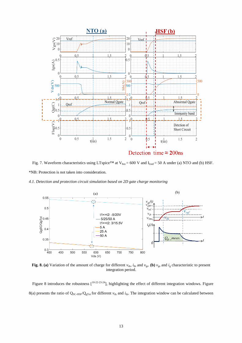
Fig. 7. Waveform characteristics using LTspice™ at Vbus = 600 V and Iload = 50 A under (a) NTO and (b) HSF.
*NB: Protection is not taken into consideration.
4.1. Detection and protection circuit simulation based on 2D gate charge monitoring
Fig. 8. (a) Variation of the amount of charge for different vds, ids and vgs. (b) vgs and ig characteristic to present
integration period.
Figure 8 introduces the robustness [10-22-23-24
], highlighting the effect of different integration windows. Figure
8(a) presents the ratio of QSC-HSF/QgTot for different vds and ids. The integration window can be calculated between
14
vgs = -5/+20 V or +3/+15.5 V. This latter setting offers a smaller QSC-HSF/QgTot ratio, which reduces the stress on
the Qg detection threshold (i.e. the lower the ratio, the easier the detection).
4.2. Detection and protection circuit simulation based on 2D derivation monitoring
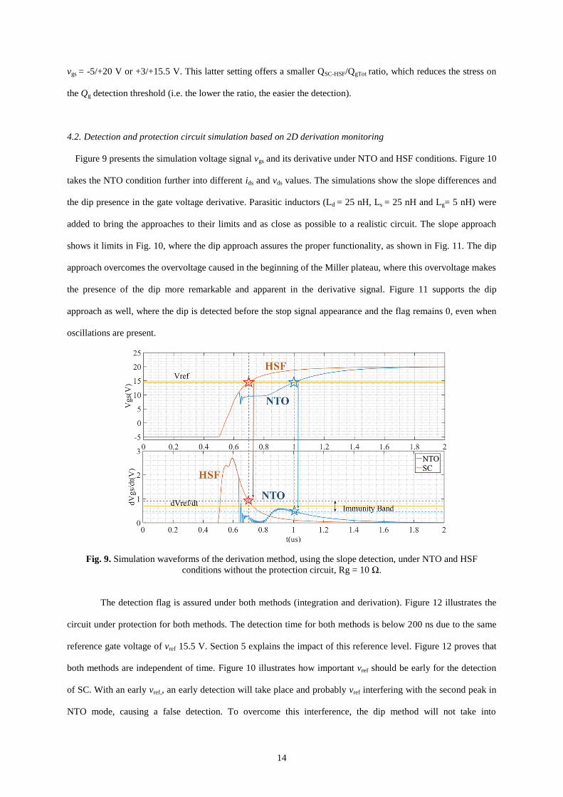
Figure 9 presents the simulation voltage signal vgs and its derivative under NTO and HSF conditions. Figure 10
takes the NTO condition further into different ids and vds values. The simulations show the slope differences and
the dip presence in the gate voltage derivative. Parasitic inductors (Ld = 25 nH, Ls = 25 nH and Lg= 5 nH) were
added to bring the approaches to their limits and as close as possible to a realistic circuit. The slope approach
shows it limits in Fig. 10, where the dip approach assures the proper functionality, as shown in Fig. 11. The dip
approach overcomes the overvoltage caused in the beginning of the Miller plateau, where this overvoltage makes
the presence of the dip more remarkable and apparent in the derivative signal. Figure 11 supports the dip
approach as well, where the dip is detected before the stop signal appearance and the flag remains 0, even when
oscillations are present.
Fig. 9. Simulation waveforms of the derivation method, using the slope detection, under NTO and HSF
conditions without the protection circuit, Rg = 10 Ω.
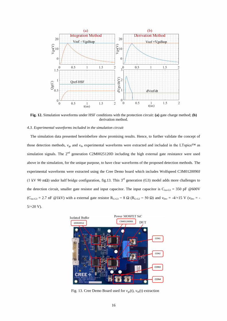
The detection flag is assured under both methods (integration and derivation). Figure 12 illustrates the
circuit under protection for both methods. The detection time for both methods is below 200 ns due to the same
reference gate voltage of vref 15.5 V. Section 5 explains the impact of this reference level. Figure 12 proves that
both methods are independent of time. Figure 10 illustrates how important vref should be early for the detection
of SC. With an early vref,, an early detection will take place and probably vref interfering with the second peak in
NTO mode, causing a false detection. To overcome this interference, the dip method will not take into
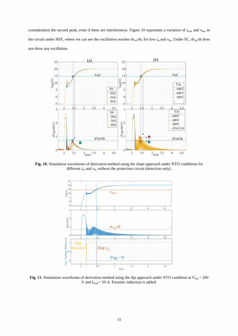
15
consideration the second peak, even if there are interferences. Figure 10 represents a variation of iload and vbus in
the circuit under HSF, where we can see the oscillation reaches dvref/dt, for low ids and vds. Under SC, dvgs/dt does
not show any oscillation.
Fig. 10. Simulation waveforms of derivation method using the slope approach under NTO conditions for
different ids and vds without the protection circuit (detection only).
Fig. 11. Simulation waveforms of derivation method using the dip approach under NTO condition at Vbus = 200
V and Iload = 50 A. Parasitic induction is added.
16
Fig. 12. Simulation waveforms under HSF conditions with the protection circuit: (a) gate charge method; (b)
derivation method.
4.3. Experimental waveforms included in the simulation circuit
The simulation data presented hereinbefore show promising results. Hence, to further validate the concept of
those detection methods, vgs and vds experimental waveforms were extracted and included in the LTspice™ as
simulation signals. The 2nd
generation C2M0025120D including the high external gate resistance were used
above in the simulation, for the unique purpose, to have clear waveforms of the proposed detection methods. The
experimental waveforms were extracted using the Cree Demo board which includes Wolfspeed C3M0120090J
(1 kV 90 mΩ) under half bridge configuration, fig.13. This 3rd
generation (G3) model adds more challenges to
the detection circuit, smaller gate resistor and input capacitor. The input capacitor is Ciss-G3 = 350 pF @600V
(Ciss-G3 = 2.7 nF @1kV) with a external gate resistor RG-G3 = 8 Ω (RG-G2 = 50 Ω) and vDrv = -4/+15 V (vDrv = -
5/+20 V).
Fig. 13. Cree Demo Board used for vgs(t), vds(t) extraction
17
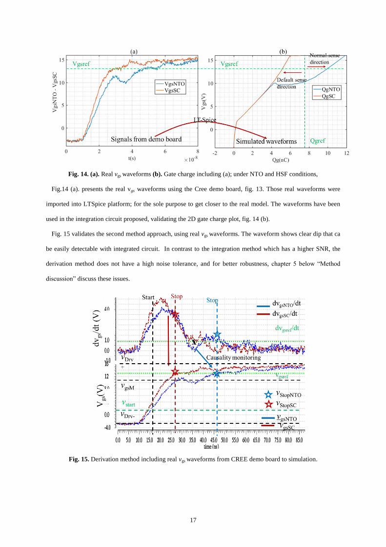
Fig. 14. (a). Real vgs waveforms (b). Gate charge including (a); under NTO and HSF conditions,
Fig.14 (a). presents the real vgs waveforms using the Cree demo board, fig. 13. Those real waveforms were
imported into LTSpice platform; for the sole purpose to get closer to the real model. The waveforms have been
used in the integration circuit proposed, validating the 2D gate charge plot, fig. 14 (b).
Fig. 15 validates the second method approach, using real vgs waveforms. The waveform shows clear dip that ca
be easily detectable with integrated circuit. In contrast to the integration method which has a higher SNR, the
derivation method does not have a high noise tolerance, and for better robustness, chapter 5 below “Method
discussion” discuss these issues.
Fig. 15. Derivation method including real vgs waveforms from CREE demo board to simulation.

18
5 Method discussion
Different detection methods proposed in the literature showed their pros and cons. Table 6. highlights diverse
aspects for the most known methods and those proposed in this article. The table shows the high integration
capability and how fast the detection comparing to the other detection methods.
Table 6. Comparison of the basic and proposed approaches related detection fault
Methods Pin Approaches Speed Cost Integration
Capability in
Gate Driver
Desaturation Drain Very Indirect -
(Blanking time)
High Voltage
sensing Diode
--
Shunt Resistor Source Straight
forward
+ High precision
Sensing resistor
-
ShuntFET
current sensing
Additional
Pin
Most Straight
forward
++ Non-Standard
Chip
+
Integration (Proposed)
Gate Indirect + Low-Voltage
Circuits
++
Derivation (Proposed)
Gate Indirect + Low-Voltage
Circuits
++
To discuss further more the proposed method, Figures 16 and 17 show a timing chart for both approaches (dip
and slope) under NTO and HSF. One can see that vgs is still rising to its saturation value. As shown in Fig. 16, the
detection starts at tstart where vgs ≈ vth and stops at tdetection where vgs = vref = vstop, at this time the detection signal
depends on the output of the third comparator, as shown in Fig. 6. The output of the third comparator signal is
neglected before and after vref. Figure 17 shows the same detection start signal, the stop signal is where vgs = vref
but it different at reading the flag. The flag is activated at tdetection the first crossing dvgs/dt and the reference
signal, where it is saved until tactivation.

19
Fig. 16. Timing chart for slope detection approach under (a) NTO and (b) HSF.
Fig. 17. Timing chart for dip detection approach under (a) NTO and (b) HSF.

20
Fig. 18. Simulation waveforms of the gate charge under NTO and HSF conditions without the protection circuit.
Figure 18 shows the impact of the vgs reference level and the critical zone. Its shows the gate charge amount in
voltage (output of the integrator) under NTO and HSF, with the waveforms based on the same simulation criteria
of Fig. 7 using LTspice™.
The discussed methods and approaches have no time dependency; however, they depend on when the gate
voltage rises above the reference level vref, so the lower this reference, the earliest the detection, with the only
condition of the vgs > vgsM. So which of these approaches is the fastest? For the gate method, Fig. 18 shows that
reducing vref is difficult due to the limitation of the Qg curve. For the derivation method, Fig. 11 shows that the
dip approach is more robust than the slope approach. Using the dip approach, we have more flexibility with the
reference level dvref/dt to cover more area for the vref reduction. With the dip approach, it can be the most robust
method allowing vgs_Ref to go lower.
6 Conclusions
This study introduces two two-dimensional detection method circuits, both of which are time independent.
Both methods protect the power circuit in the event of a SC. The gate charge method exhibits a fast detection and
protection capability and introduces less SNR under NTO and HSF. The reference levels are the critical values
for both methods. The derivation method is presented with two approaches. With the slope approach, oscillation
can slightly distort the detection, if the detection is at a critical vref (dvref/dt interfering with dvgs/dt). In contrast,
the dip approach is better due to the dip transition, under NTO conditions, even with dvref/dt interfering with
dvgs/dt, the detection of a dip occurs before the interference of the second peak. Under HSF, no oscillations are
present for both approaches.
For robustness and fast detection, the higher the dvref/dt and the lower the vref, the better. In other words, setting
dvref/dt higher, will prevent interference. Defining a low vref, allows for early detection.
21
In future works, the authors will implement experimentally and compare with the simulations. Several
limitations must be particularly addressed, such as the precise assessment of the threshold voltages with the dip
method, the effects of parasitic elements and non-ideal circuits.
Acknowledgements
This research work has been supported financially by the French Ministry in higher education, research and
innovation.
References
[1] Baliga, B.J. Silicon Carbide Power Devices. World Scientific, 2005.
[2] Wang, Z., et al. Design and Performance Evaluation of Overcurrent Protection Schemes for Silicon
Carbide (SiC) Power MOSFETs. IEEE TIEs 61, 5570–5581 (2014).
[3] Musumeci, S., et al. A new gate circuit performing fault protections of IGBTs during short circuit
transients. in Conference Record of the 2002 IEEE IAS. 4, 2614–2621 (2002).
[4] Bertelshofer, T. Design Rules to Adapt the Desaturation Detection for SiC MOSFET Modules. 8
(2017).
[5] Luo, H. et al. Modern IGBT gate driving methods for enhancing reliability of high-power converters —
An overview. Microelectronics Reliability 58, 141–150 (2016).
[6] Kudoh, M., et al. Current sensing IGBT for future intelligent power module. ISPSD ’96. Proceedings
303–306 (1996).
[7] Oberdieck, K. et al. W. Short circuit detection using the gate charge characteristic for Trench/Fieldstop-
IGBTs. in EPE’16 ECCE Europe 1–10 (2016).
[8] Cui, M., Li, J., Du, Y. and Zhao, Z. Behavior of SiC MOSFET under Short-Circuit during the On-State,
IOP Conf. Ser. Mater. Sci. Eng., 439, p. 022026 (2018).
[9] IDchar, I., Zolkos, M., Buttay, C. and Morel, H, Robustness of SiC MOSFET under avalanche
conditions, in 2017 IEEE Applied Power Electronics Conference and Exposition (APEC), Tampa, FL,
USA, 2017, p. 2263‑ 2268 (2017).
[10] Chen, C., Labrousse, D., Lefebvre, S., Petit, M., Buttay, C. and Morel, H. Study of short-circuit
robustness of SiC MOSFETs, analysis of the failure modes and comparison with BJTs, Microelectron.
Reliab., vol. 55, no 9‑ 10, p. 1708‑ 1713 (2015).

22
[11] Bhatnagar, M. and Baliga, B.J. Comparison of 6H-SiC, 3C-SiC, and Si for power devices, IEEE Trans.
Electron Devices, vol. 40, no 3, p. 645‑ 655, (1993).
[12] Balogh, L. Fundamentals of MOSFET and IGBT Gate Driver Circuits. 48 (2017).
[13] Vrej Barkhordarian. Power MOSFET Basics. International Rectifier
[14] Semiconductor Components Industries, MOSFET Gate Charge Origin and its Applications. Application
note, Publication order number AND9083/D. Februrary,2016 – Rev. 2
[15] Horiguchi, T. et al. Short-Circuit Protection Method Based on a Gate Charge Characteristic. IEEJ 4,
360–369 (2015).
[16] Horiguchi, T., Kinouchi, S., Nakayama, Y. & Akagi, H. A fast short-circuit protection method using
gate charge characteristics of SiC MOSFETs. in 2015 ECCE 4759–4764 (2015).
[17] Park, B.-G., Lee, J.-B. & Hyun, D.-S. A Novel Short-Circuit Detecting Scheme Using Turn-On
Switching Characteristic of IGBT. in 2008 IEEE IASAM 1–5 IEEE, 2008
[18] J. Acuna, J. Walter and I. Kallfass, Very Fast Short Circuit Protection for Gallium-Nitride Power
Transistors Based on Printed Circuit Board Integrated Current Sensor. 2018 20th European Conference
on Power Electronics and Applications (EPE'18 ECCE Europe), Riga, 2018, pp. P.1-P.10.
[19] P. Hofstetter, S. Hain and M. Bakran. Applying the 2D-Short Circuit Detection Method to SiC
MOSFETs including an advanced Soft Turn Off. PCIM Europe 2018; International Exhibition and
Conference for Power Electronics, Intelligent Motion, Renewable Energy and Energy Management,
Germany, 2018, pp. 1-7.
[20] X. Li, D. Xu, H. Zhu, X. Cheng, Y. Yu, et W. T. Ng. Indirect IGBT Over-Current Detection Technique
Via Gate Voltage Monitoring and Analysis. IEEE Trans. Power Electron., vol. 34, no 4, p. 3615‑ 3622,
avr. 2019.
[21] F. Boige, F. Richardeau, S. Lefebvre et al.Mathematics and Computers in Simulation 158 (2019) 375–
386
[22] T. Nguyen, A. Ahmed, T. V. Thang and J. Park. Gate Oxide Reliability Issues of SiC MOSFETs Under
Short-Circuit Operation. in IEEE Transactions on Power Electronics, vol. 30, no. 5, pp. 2445-2455, May
2015. doi: 10.1109/TPEL.2014.2353417
[23] F. Chimento and M. Nawaz. On the short circuit robustness evaluation of silicon carbide high power
modules. 2015 IEEE Energy Conversion Congress and Exposition (ECCE), Montreal, QC, 2015, pp.
920-926. doi: 10.1109/ECCE.2015.7309786

23
[24] J. Ortiz Gonzalez, R. Wu, S.N. Agbo, O. Alatise. Robustness and reliability review of Si and SiC FET
devices for more-electric-aircraft applications. Microelectronics Reliability, Elsevier (2019).