computer architecture lecture 21 memory hierarchy design
Post on 21-Dec-2015
224 views
TRANSCRIPT

Computer Architecture
Lecture 21
Memory Hierarchy Design
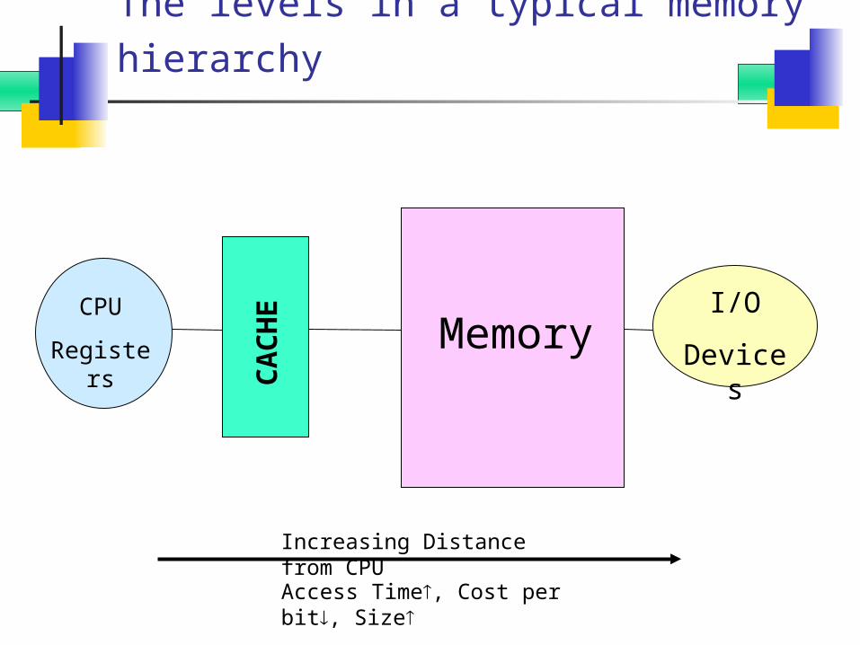
The levels in a typical memory hierarchy
CPU
Registers
CA
CH
EMemory
I/O
Devices
Increasing Distance from CPUAccess Time, Cost per bit, Size

Cache performance review
Level 1 2 3 4
Name Registers Cache Main memory
Disk storage
Typical size <1KB < 16MB < 16 GB > 200 GB
Technology Custom mem. With multiple
ports
On-chip CMOS SRAM
CMOS DRAM Magnetic disk
Access time (ns)
0.25-0.5 0.5-25 45-250 5,000,000
Bandwidth (MB/sec)
50,000-1000,000
2000-50,000
1000-3000 20-150
Managed by Compiler Hardware Operating system
Operating sys
Backed by cache Main memory Disk CD or tape

Performance baseline, the gap in performance
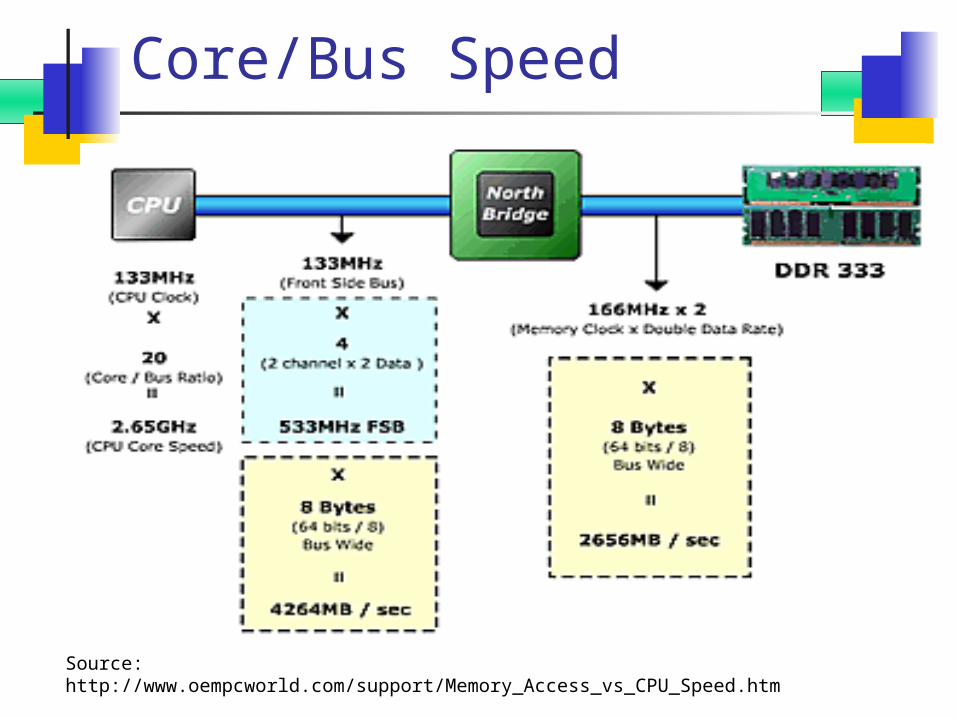
Core/Bus Speed
Figure: Memory Access Speed
Source: http://www.oempcworld.com/support/Memory_Access_vs_CPU_Speed.htm

Basic Philosophy
Temporal Locality Spatial Locality
Review of the ABCs of Caches
Victim Cache Fully associative Write allocate
Non-Blocking Dirty bit Unified cache
Mem. stall cycles Block offset Misses/instruction
Direct mapped Write back Block
Valid bit Data cache Locality
Block address Hit time Address trace
Write through Cache miss Set
Instr. Cycle Page fault Trace CacheAMAT Miss rate Index field
Cache hit Set Associative No-write allocate
Page LRU Write buffer
Miss penalty Tag field Write stall
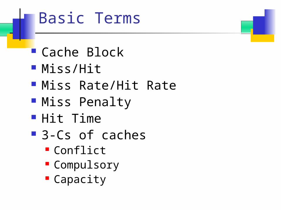
Basic Terms
Cache Block Miss/Hit Miss Rate/Hit Rate Miss Penalty Hit Time 3-Cs of caches
Conflict Compulsory Capacity
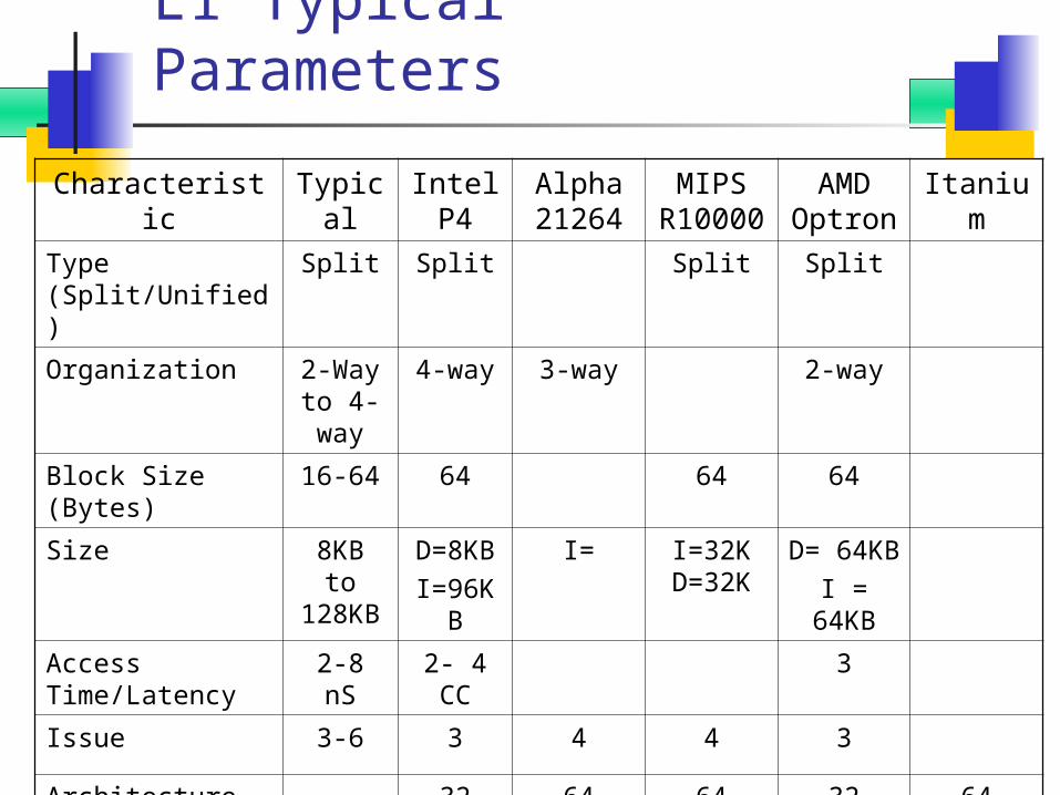
L1 Typical Parameters
Characteristic Typical
Intel P4
Alpha 21264
MIPS R1000
0
AMD Optron
Itanium
Type (Split/Unified)
Split Split Split Split
Organization 2-Way to 4-way
4-way 3-way 2-way
Block Size (Bytes)
16-64 64 64 64
Size 8KB to 128KB
D=8KB
I=96KB
I= I=32K D=32K
D= 64KBI =
64KB
Access Time/Latency
2-8 nS 2- 4 CC
3
Issue 3-6 3 4 4 3
Architecture 32 64 64 32 64
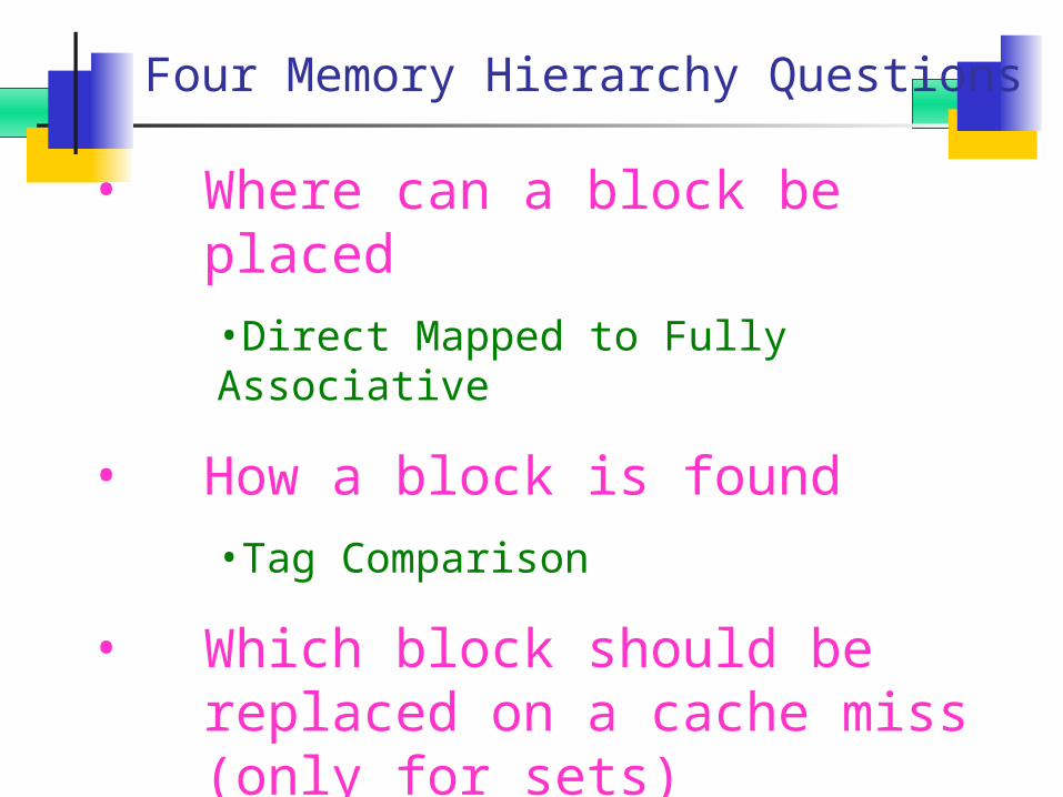
Four Memory Hierarchy Questions
• Where can a block be placed•Direct Mapped to Fully Associative
• How a block is found•Tag Comparison
• Which block should be replaced on a cache miss (only for sets)•LRU, Random, FIFO (Levels off > 256KB)

Direct Mapped CacheAssume 5-bit address bus and cache with 8 entries
000001010011100101110111
Processor
D2 - D0
D4 – D3
TAG
Data Bus
IndexTAG
HIT DATA
Index
= HIT
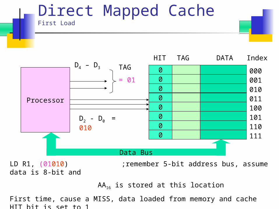
Direct Mapped CacheFirst Load
000001010011100101110111
Processor
D2 - D0 = 010
D4 – D3 TAG
= 01
IndexTAG0
0000000
HIT DATA
Data Bus
LD R1, (01010) ;remember 5-bit address bus, assume data is 8-bit and
AA16 is stored at this location
First time, cause a MISS, data loaded from memory and cache HIT bit is set to 1
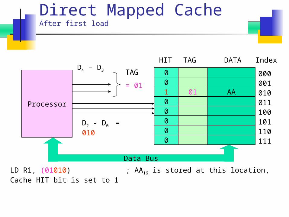
Direct Mapped CacheAfter first load
000001
AA 010011100101110111
Processor
D2 - D0 = 010
D4 – D3 TAG
= 0101
00100000
Data Bus
LD R1, (01010) ; AA16 is stored at this location, Cache HIT bit is set to 1
IndexTAG
HIT DATA

Direct Mapped CacheSecond Load
000001
AA 010011100101110111
Processor
D2 - D0 = 010
D4 – D3TAG
= 11
01
00100000
Data Bus
LD R1, (11010) ; assume 99 at address 11010
Same index but different TAG will cause a MISS, data loaded from memory
IndexTAG
HIT DATA

Direct Mapped CacheAfter Second Load
000001
99 010011100101110111
Processor
D2 - D0 = 010
D4 – D3 TAG
= 1111
00100000
Data Bus
LD R1, (11010) ;remember 5-bit address bus, assume 99
First time, same index but different TAG will cause a MISS, data loaded from memory
IndexTAG
HIT DATA
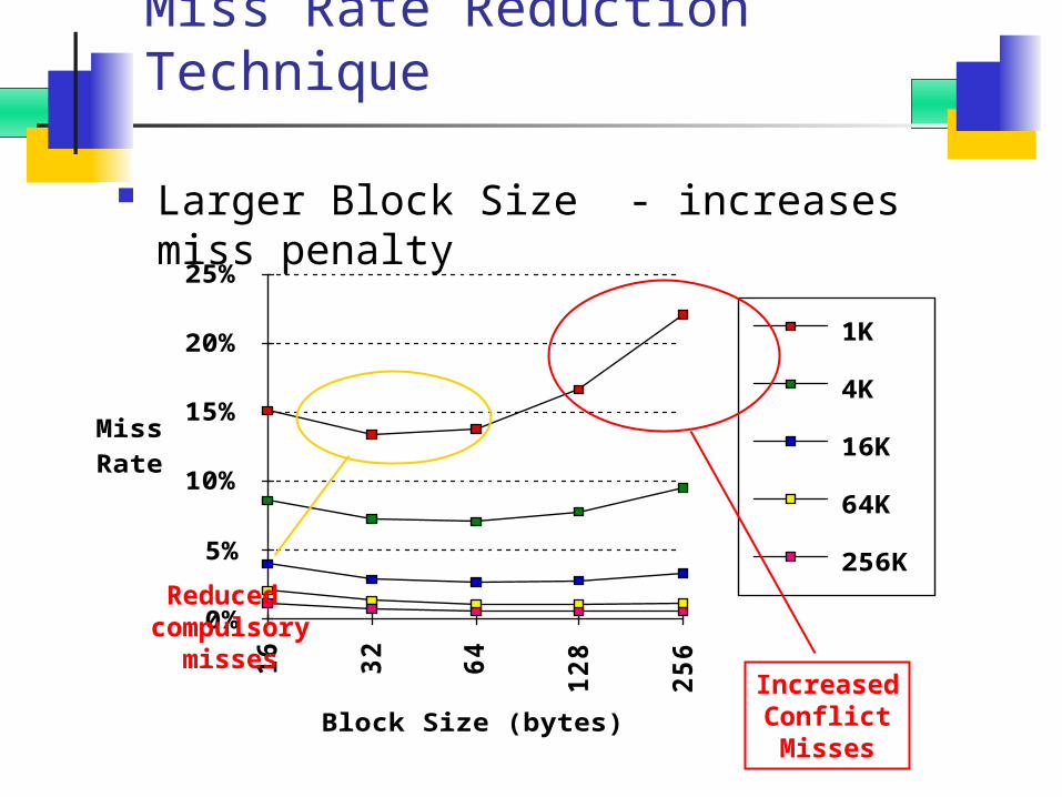
Miss Rate Reduction Technique
Larger Block Size - increases miss penalty
Block Size (bytes)
Miss Rate
0%
5%
10%
15%
20%
25%1
6
32
64
12
8
25
6
1K
4K
16K
64K
256K
IncreasedConflictMisses
Reduced compulsory
misses
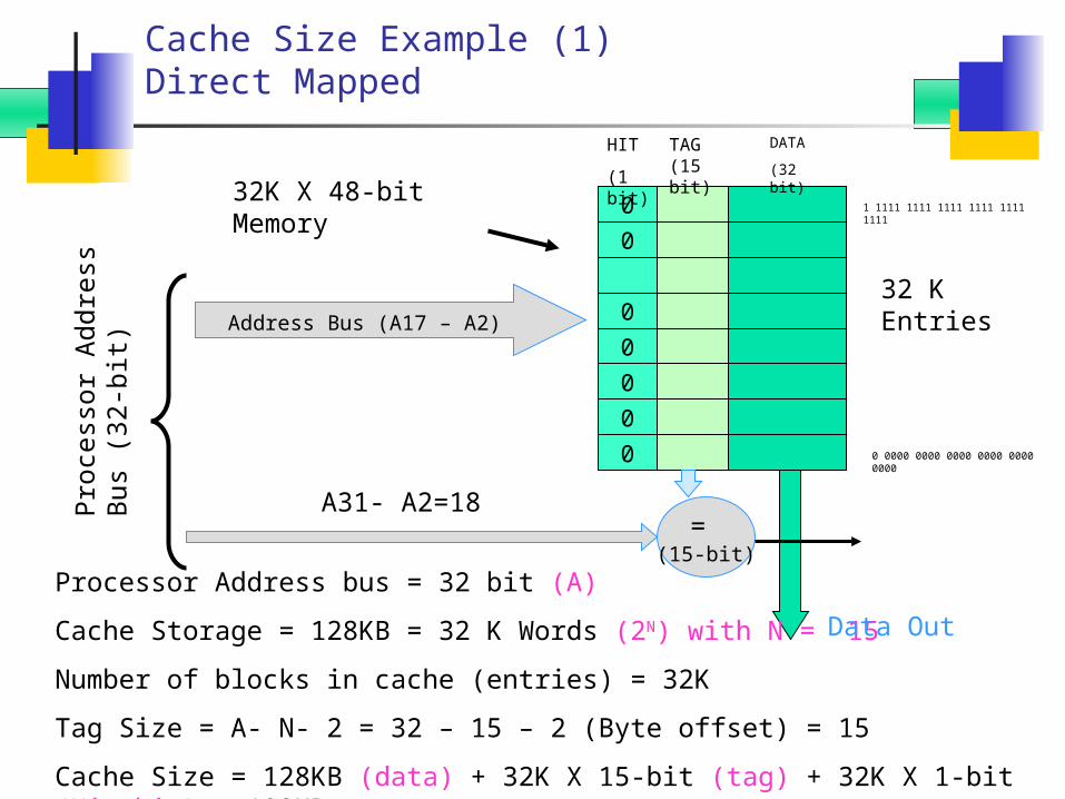
Cache Size Example (1)Direct Mapped
0
0
0
0
0
0
0
TAG (15 bit)
HIT
(1 bit)
DATA
(32 bit)
Processor Address bus = 32 bit (A)
Cache Storage = 128KB = 32 K Words (2N) with N = 15
Number of blocks in cache (entries) = 32K
Tag Size = A- N- 2 = 32 – 15 – 2 (Byte offset) = 15
Cache Size = 128KB (data) + 32K X 15-bit (tag) + 32K X 1-bit (Hit bit) = 192KB
Address Bus (A17 – A2) 32 K Entries
0 0000 0000 0000 0000 0000 0000
1 1111 1111 1111 1111 1111 1111
32K X 48-bit Memory
Pro
cess
or
Addre
ss B
us
(32-b
it)
= (15-bit)
Data Out
A31- A2=18
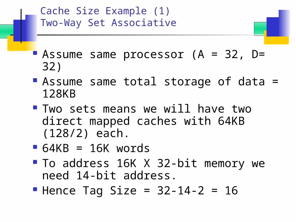
Cache Size Example (1)Two-Way Set Associative
Assume same processor (A = 32, D= 32)
Assume same total storage of data = 128KB
Two sets means we will have two direct mapped caches with 64KB (128/2) each.
64KB = 16K words To address 16K X 32-bit memory we
need 14-bit address. Hence Tag Size = 32-14-2 = 16
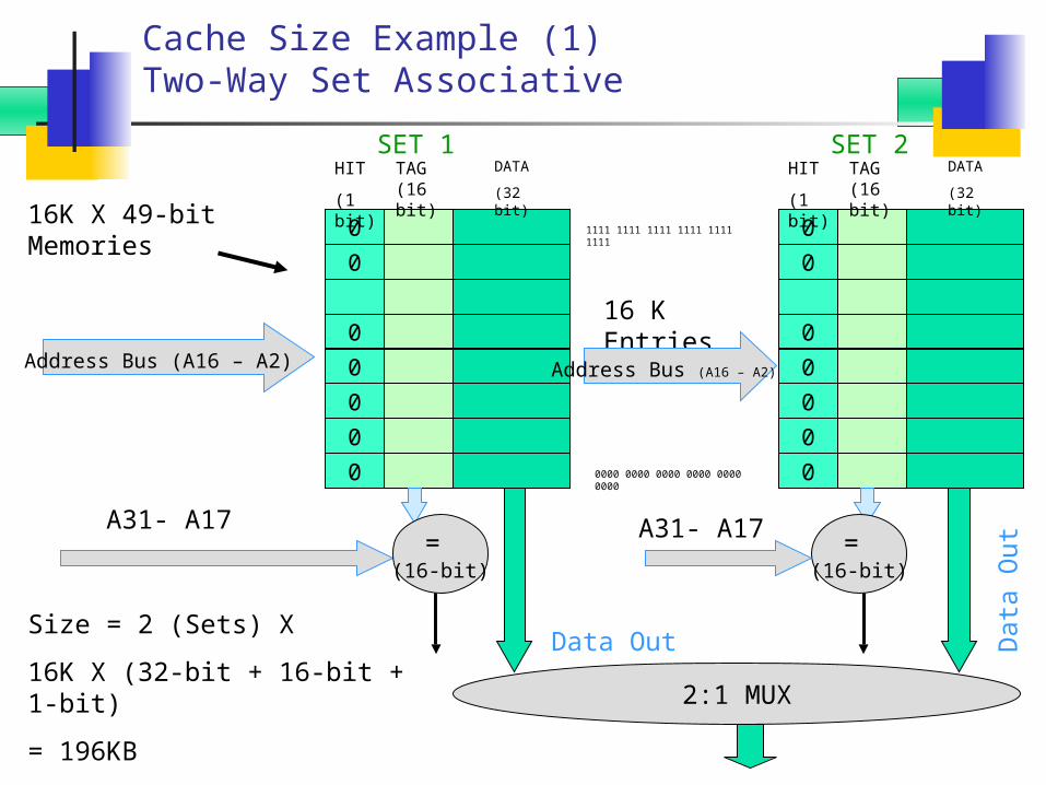
Cache Size Example (1)Two-Way Set Associative
0
0
0
0
0
0
0
TAG (16 bit)
HIT
(1 bit)
DATA
(32 bit)
Address Bus (A16 – A2)
16 K Entries
0000 0000 0000 0000 0000 0000
1111 1111 1111 1111 1111 1111
16K X 49-bit Memories
= (16-bit)
Data Out
A31- A17
SET 1
0
0
0
0
0
0
0
TAG (16 bit)
HIT
(1 bit)
DATA
(32 bit)
= (16-bit)
SET 2
Address Bus (A16 – A2)
A31- A17
Data
Out
2:1 MUX
Size = 2 (Sets) X
16K X (32-bit + 16-bit + 1-bit)
= 196KB
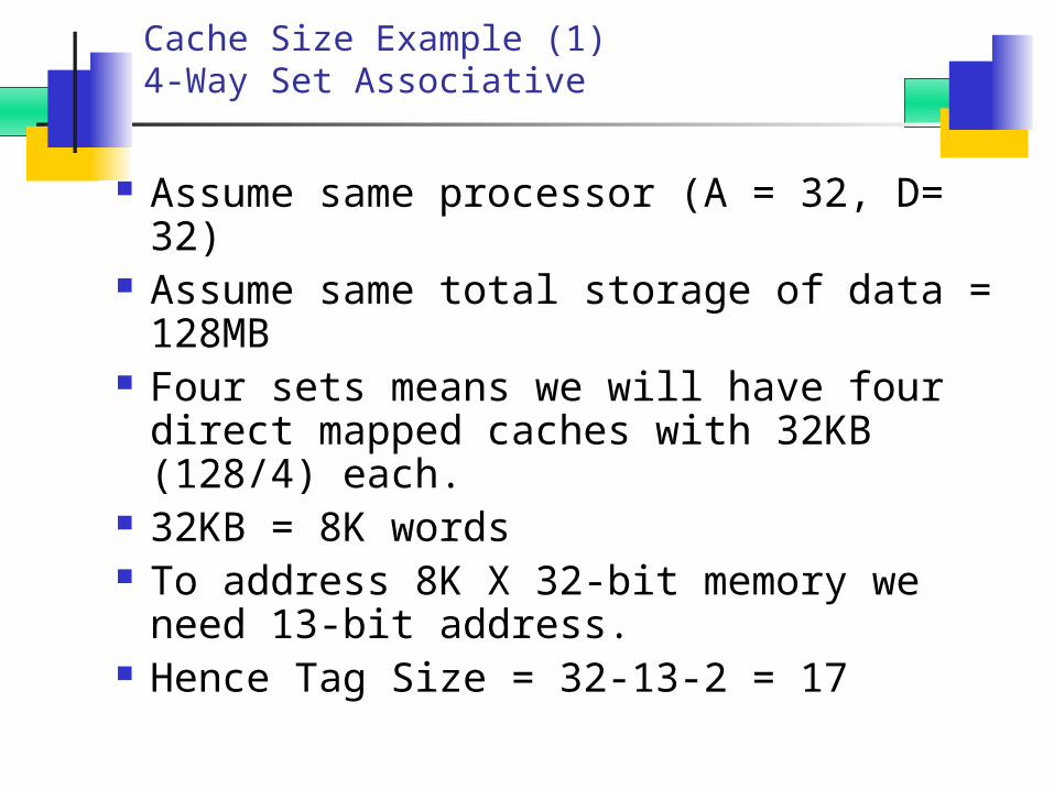
Cache Size Example (1)4-Way Set Associative
Assume same processor (A = 32, D= 32)
Assume same total storage of data = 128MB
Four sets means we will have four direct mapped caches with 32KB (128/4) each.
32KB = 8K words To address 8K X 32-bit memory we need
13-bit address. Hence Tag Size = 32-13-2 = 17

Cache Size Example (1)4-Way Set Associative
0
0
0
0
0
0
0
Address Bus (A15 – A2)
8 M Entries
8K X 50-bit Memories
= (17-bit)
A31- A16
SET 1
0
0
0
0
0
0
0
= (17-bit)
SET 2
A31- A16
Data
Out
4:1 MUX
Size = 4 (Sets) X
8K X (32-bit + 7-bit + 1-bit)
= 200KB
8 M Entries
0
0
0
0
0
0
0
= (17-bit)
SET 3
A31- A16
Data
Out
8 M Entries
Data Out to processor
0
0
0
0
0
0
0
TAG
17
HIT
= (17-bit)
SET 4
Address Bus (A15 – A2)
A31- A16
Data
Out
Address Bus (A15 – A2) Address Bus
(A15 – A2)
TAG
17
HITTAG
17
HITTAG
17
HIT
8-Way Set associative Cache?
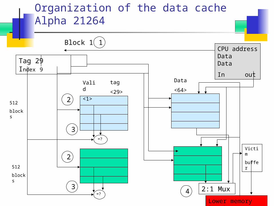
Organization of the data cache Alpha 21264
512
blocks
512
blocks
Tag 29 Index 9
Valid
<1>
tag
<29>
Data
<64>
2:1 Mux
CPU address Data Data
In out
Lower memory level
=?
=?
Victim
buffer
Block 1 1
2
3
2
34
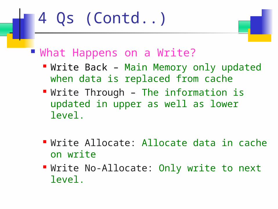
4 Qs (Contd..)
What Happens on a Write? Write Back – Main Memory only updated
when data is replaced from cache Write Through – The information is
updated in upper as well as lower level.
Write Allocate: Allocate data in cache on write
Write No-Allocate: Only write to next level.
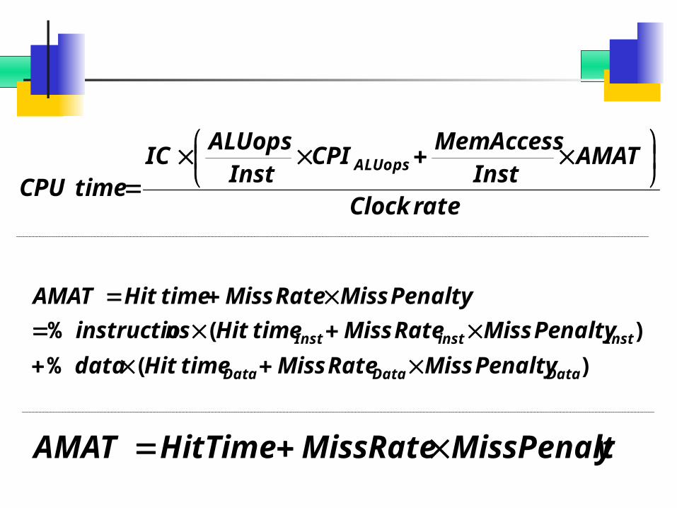
rateClock
AMATInst
MemAccessCPI
InstALUops
ICtimeCPU
ALUops
)(%
)(%
DataDataData
InstinstInst
PenaltyMissRateMisstimeHitdata
PenaltyMissRateMisstimeHitnsinstructio
PenaltyMissRateMisstimeHitAMAT
yMissPenaltMissRateHitTimeAMAT
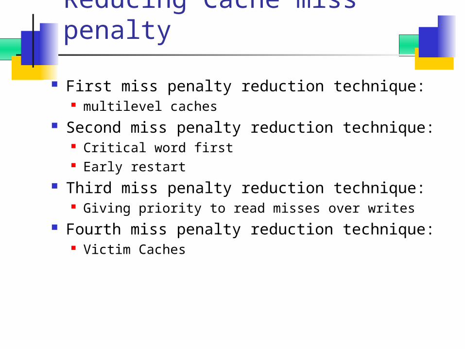
Reducing Cache miss penalty
First miss penalty reduction technique: multilevel caches
Second miss penalty reduction technique: Critical word first Early restart
Third miss penalty reduction technique: Giving priority to read misses over writes
Fourth miss penalty reduction technique: Victim Caches
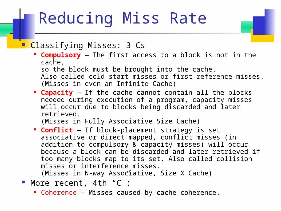
Reducing Miss Rate
Classifying Misses: 3 Cs Compulsory — The first access to a block is not in the
cache, so the block must be brought into the cache. Also called cold start misses or first reference misses.(Misses in even an Infinite Cache)
Capacity — If the cache cannot contain all the blocks needed during execution of a program, capacity misses will occur due to blocks being discarded and later retrieved.(Misses in Fully Associative Size Cache)
Conflict — If block-placement strategy is set associative or direct mapped, conflict misses (in addition to compulsory & capacity misses) will occur because a block can be discarded and later retrieved if too many blocks map to its set. Also called collision misses or interference misses.(Misses in N-way Associative, Size X Cache)
More recent, 4th “C”: Coherence — Misses caused by cache coherence.
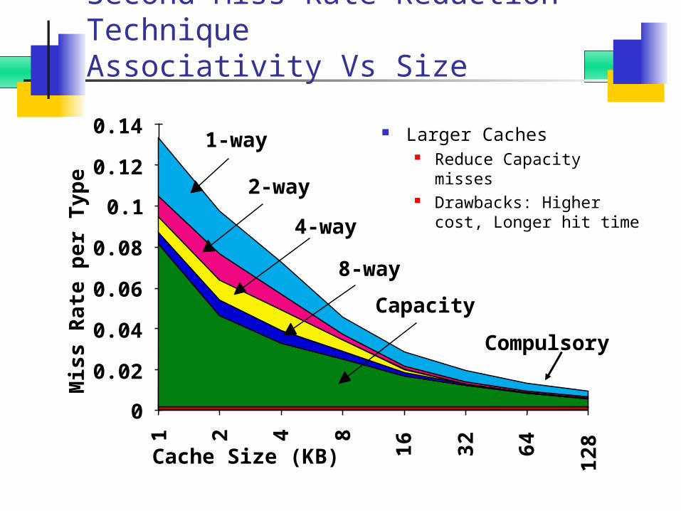
Second Miss Rate Reduction TechniqueAssociativity Vs Size
Larger Caches Reduce Capacity misses Drawbacks: Higher cost,
Longer hit time
Cache Size (KB)
Mis
s R
ate
per
Typ
e
0
0.02
0.04
0.06
0.08
0.1
0.12
0.14
1 2 4 8
16
32
64
128
1-way
2-way
4-way
8-way
Capacity
Compulsory
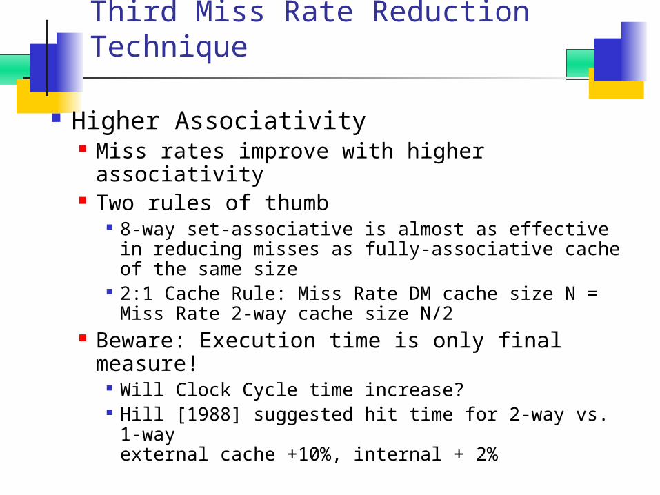
Third Miss Rate Reduction Technique
Higher Associativity Miss rates improve with higher associativity Two rules of thumb
8-way set-associative is almost as effective in reducing misses as fully-associative cache of the same size
2:1 Cache Rule: Miss Rate DM cache size N = Miss Rate 2-way cache size N/2
Beware: Execution time is only final measure! Will Clock Cycle time increase? Hill [1988] suggested hit time for 2-way vs. 1-way
external cache +10%, internal + 2%
Example
Given Statistics Load/Store Instructions: 50% Hit Time = 2 Clock Cycles, Hit rate = 90%Miss Penalty = 40 CC____________________________________Average Memory Access /instruction =
1.5Ave. Mem Access Time =
Hit time + Miss rate * Miss Penalty = 2 + 0.1 *40 = 2 + 4 = 6
; 4 is Penalty CyclesCPI = ?CPI (with perfect cache) = 2CPI (overall) =
CPI (perfect) + Extra Memory Stall Cycles/Instruction (penalty Cycles)
= 2 + (6 – 2) * 1.5= 2 + 6 = 8
Number of instructions MethodAssume total instructions = 1000Perfect CacheEach instruction takes 2 clock cycles,
hence 1000 * 2 = 2000Clock cyclesCPI (Perfect) = CC/IC = 2000/1000 = 2
Imperfect CacheCalculate Extra Clock CycleNumber memory access = 1000 * 1.5
( 1000 for I$ and 500 for D$) = 1500 Memory access in 1000
Instruction program.Cache missed (at 10%) = 1500 * 0.1 =
150Extra(Penalty) Clock Cycles for Missed
Cache = 150 * 40 = 6000Which is infact:
= IC (Mem Access/Instruc) * Miss Rate * Miss Penalty
Total clock cycle for instruction with perfect cache = 2000 Clock Cycles
Total for Program = 2000 + 6000 = 8000
CPI = 8000/1000 = 8.0

Example with 2-level Cache
Stats: L1: Hit Time = 2 Clock Cycles, Hit rate = 90%, Miss Penalty to L2 = 10 CC (Hit time for L2) L2: Local Hit Rate = 80%, Miss Penalty(L2)= 40 CCLoad/Store Instructions: 50%
CPU
L
1
L
2
HT= 2 CC
Hit rate = 90%,
Out of 100 Memory Accesses: 20 Miss
Main
Memory
HT = 40 CC Global Miss Rate = ?
1000 Memory Accesses: 100 Miss

Example 1
Once again Perfect Cache CPI = 2.0AMAT = Hit TimeL1 + Miss Rate1 (Hit
TimeL2 + Miss rateL2 Miss PenaltyL2)= 2 + 0.1 (10 + 0.2 40) = 3.8
CPI = CPI perfect + Extra Memory Stall Cycles/instruction
= 2.0 + (3.8-2) 1.5 = 4.7
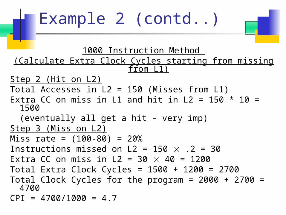
Example 2 (contd..)
1000 Instruction Method (Calculate Extra Clock Cycles starting from missing from
L1)Step 2 (Hit on L2)Total Accesses in L2 = 150 (Misses from L1)Extra CC on miss in L1 and hit in L2 = 150 * 10 = 1500
(eventually all get a hit – very imp) Step 3 (Miss on L2)Miss rate = (100-80) = 20%Instructions missed on L2 = 150 .2 = 30Extra CC on miss in L2 = 30 40 = 1200Total Extra Clock Cycles = 1500 + 1200 = 2700Total Clock Cycles for the program = 2000 + 2700 =
4700CPI = 4700/1000 = 4.7
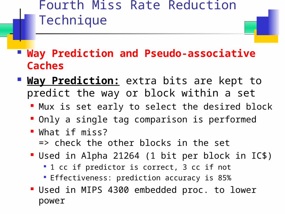
Fourth Miss Rate Reduction Technique
Way Prediction and Pseudo-associative Caches
Way Prediction: extra bits are kept to predict the way or block within a set Mux is set early to select the desired block Only a single tag comparison is performed What if miss?
=> check the other blocks in the set Used in Alpha 21264 (1 bit per block in IC$)
1 cc if predictor is correct, 3 cc if not Effectiveness: prediction accuracy is 85%
Used in MIPS 4300 embedded proc. to lower power
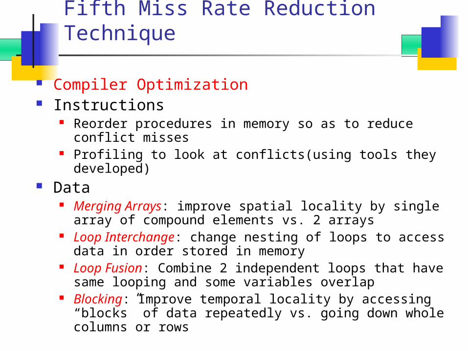
Fifth Miss Rate Reduction Technique
Compiler Optimization Instructions
Reorder procedures in memory so as to reduce conflict misses
Profiling to look at conflicts(using tools they developed) Data
Merging Arrays: improve spatial locality by single array of compound elements vs. 2 arrays
Loop Interchange: change nesting of loops to access data in order stored in memory
Loop Fusion: Combine 2 independent loops that have same looping and some variables overlap
Blocking: Improve temporal locality by accessing “blocks” of data repeatedly vs. going down whole columns or rows
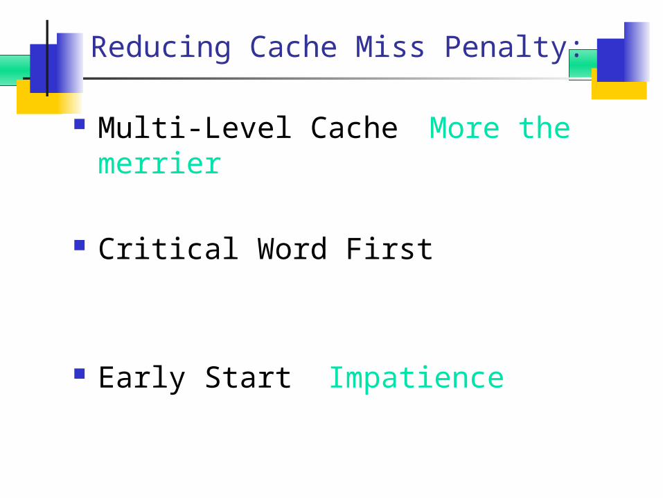
Reducing Cache Miss Penalty:
Multi-Level CacheMore the merrier
Critical Word First
Early Start Impatience

Reducing Cache Miss Penalty:
Give priority to Read over Write; Preference
Reducing Cache Miss Penalty:
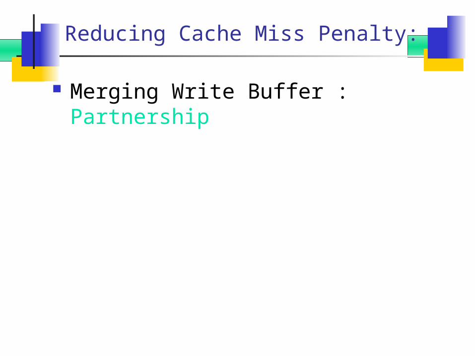
Merging Write Buffer : Partnership

Reducing Cache Miss Penalty:
Victim Cache: recycling
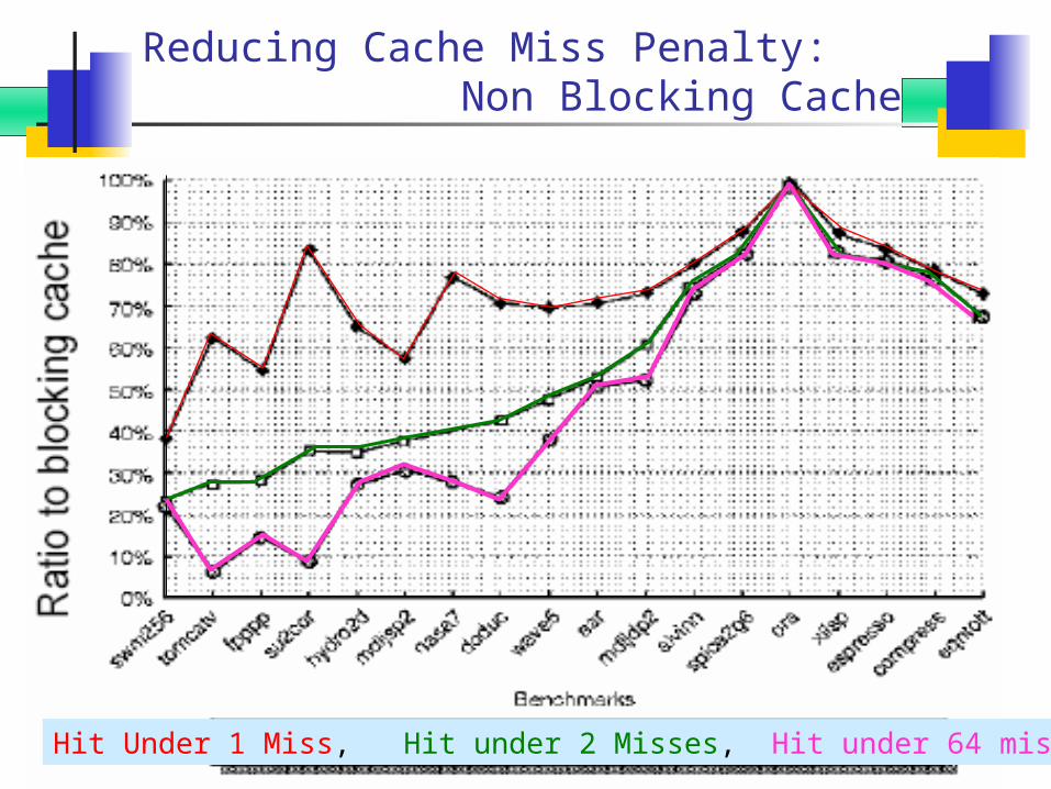
Reducing Cache Miss Penalty: Non Blocking Cache
Hit Under 1 Miss, Hit under 2 Misses, Hit under 64 misses
Reducing Cache Miss Penalty or Miss Rate
Miss Penalty/Rate Reduction Technique: Hardware Perfetching of Instruction
and Data Miss Penalty/Rate Reduction
Technique: Compiler-Controlled Prefetching
Register Perfetching Cache Perfetching
Reducing Hit Time
First Hit Time Reduction Technique: Small and Simple Caches
Second Hit Time Reduction Technique: Avoiding Address Translation during
Indexing of the Cache Third Hit Time Reduction Technique:
Pipelining Cache Access Fourth Hit Time Reduction Technique:
Trace Caches
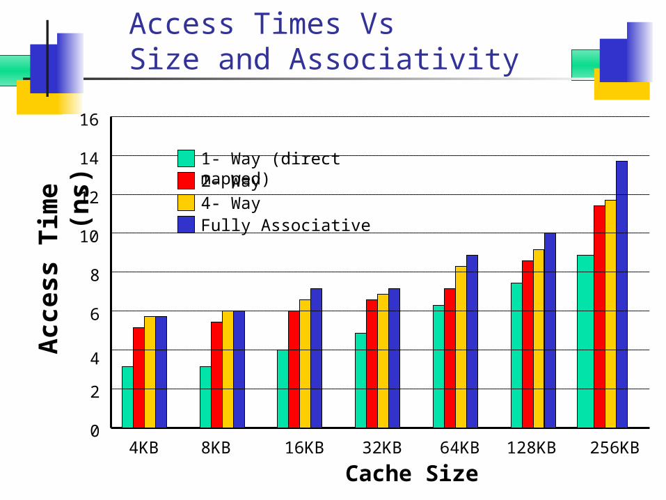
Access Times Vs Size and Associativity
4KB 8KB 16KB 32KB 64KB 128KB
256KBCache Size
0
2
4
6
8
10
12
14
16
Access T
ime
(ns) 1- Way (direct
mapped)2- Way 4- WayFully Associative

Main memory and Organization for Improving Performance
Techniques for Higher Bandwidth Wider Main Memory Simple Interleaved memory Independent Memory Banks