concept paper of the astron project d7.3
TRANSCRIPT

ADAPTIVE SOFTWARE DEFINED TERABIT TRANSCEIVER FOR FLEXIBLE OPTICAL NETWORKS
FP7‐ICT‐GA 318714
SPECIFIC TARGETED RESEARCH PROJECT (STREP) INFORMATION & COMMUNICATION TECHNOLOGIES (ICT)
Concept paper of the ASTRON project
D7.3
Document Type: Deliverable
Dissemination Level: PP1
Lead Beneficiary: AIT
Contact Person: Panagiotis Zakynthinos (email: [email protected])
Delivery Due Date: 30/09/2013
Submission date: 29/11/2013
Contributing institutes: All beneficiaries
Authors: Panagiotis Zakynthinos (AIT), Ioannis Tomkos (AIT), Moshe Nazarathy (TECHNION), Alex Tolmachev (TECHNION), Ronald Kaiser (HHI), Braulio Gomez Saavedra (HHI), Polina Bayvel (UCL), Robert Killey (UCL), Gabriella Cincotti (RM3), Julian Hoxha (RM3) Shalva Ben‐Ezra (FINISAR), Nicholas Psaila (OPTOSCRIBE), Mayra Irion (ALBIS), Vincent Grundlehner (ALBIS), Gunther Vollrath (AIFOTEC), Roberto Magri (TEI), Marianna Angelou (OPTRONICS)
Reviewers: All beneficiaries
1 PU = Public PP = Restricted to other programme participants (including the Commission Services) RE = Restricted to a group specified by the consortium (including the Commission Services) CO = Confidential, only for members of the consortium (including the Commission Services)

Concept paper of the ASTRON project Version 1.0
FP7‐ICT‐GA 318714 Confidential Document 1 | P a g e
The ASTRON Project Consortium
No Partner Name Short Name Country
1 OPTRONICS TECHNOLOGIES A.B.E.T.E. OPTRONICS Greece
2 FINISAR ISRAEL LTD FINISAR Israel
3 FRAUNHOFER‐GESELLSCHAFT ZUR FOERDERUNG DER ANGEWANDTEN FORSCHUNG E.V‐HEINRICH HERTZ INSTITUT
HHI Germany
4 RESEARCH AND EDUCATION LABORATORY IN INFORMATION TECHNOLOGIES
AIT Greece
5 UNIVERSITY COLLEGE LONDON UCL United Kingdom
6 UNIVERSITA DEGLI STUDI ROMA TRE RM3 Italy
7 ALBIS OPTOELECTRONICS AG ALBIS Switzerland
8 AIFOTEC AG AIFOTEC Germany
9 ERICSSON TELECOMUNICAZIONI TEI Italy
10 NATIONAL INSTITUTE OF INFORMATION AND COMMUNICATIONS TECHNOLOGY
NICT Japan
11 OPTOSCRIBE LTD OPTOSCRIBE United Kingdom
12 TECHNION‐ISRAEL INSTITUTE OF TECHNOLOGY TECHNION Israel
“The research leading to these results has received funding from the European Community's Seventh Framework Programme (FP7/2007‐2013) under grant agreement n° 318714”.

Concept paper of the ASTRON project Version 1.0
FP7‐ICT‐GA 318714 Confidential Document 2 | P a g e
Revision History
No. Version Author(s) Date
1 0.1 Panagiotis Zakynthinos 22/11/13
2 0.2 Moshe Nazarathy, Alex Tolmachev (TECHNION) 26/11/13
3 0.3 Nicholas Psaila (OPTOSCRIBE) 27/11/13
4 0.4 Mayra Irion (ALBIS) 27/11/13
5 0.5 Roberto Magri (TEI) 27/11/13
6 0.6 Ronald Kaiser, Braulio Gomez Saavedra (HHI) 27/11/13
7 0.7 Gabriella Cincotti, Julian Hoxha (RM3) 27/11/13
8 0.8 Polina Bayvel, Robert Killey (UCL) 27/11/13
9
10
11

FP7‐ICT‐GA 318714 Confidential Document 3 | P a g e
3
Abstract—Flexible optical networking has been introduced recently as a way to offer efficient utilization of the available optical resources. Flexible transceivers capable to generate and receive tributaries with variable bandwidth characteristics are key subsystem elements for the realization of a flexible optical networking system. This paper presents the main concept and developments envisioned by the EU funded project ASTRON, which targets the design, development and evaluation of a high-capacity, energy-efficient and bit-rate flexible optical transceiver capable of supporting rates from 10Gb/s to beyond 1Tb/s. The ASTRON technology relies on the combination of InP monolithic chips and Silica planar lightwave circuits to develop compact photonic integrated modules that exploit hybrid integration technologies.
I. INTRODUCTION The emergence of bandwidth-consuming and highly dynamic services, dictates the evolution of old fixed optical networks that were based on wavelength division multiplexing (WDM). Traditional WDM-based networks
offer the possibility to establish fixed connections (wavelengths) and bit rates, namely 10 Gb/s, 40 Gb/s, and recently 100 Gb/s, where the channels are modulated with a common (pre-defined) modulation format (e.g. On-Off Keying (OOK), Differential Phase Shift Keying (DPSK) or Quadrature Phase Shift Keying(QPSK)) and are spaced at a fixed channel spacing of 50 GHz. Flexibility in these networks is limited to that allowed by frequency-tunable lasers (i.e., each transponder can be assigned to a different wavelength) and to the limited reconfigurations allowed by optical switching nodes. As a result, the process of upgrading/modifying the network to adapt to changing traffic and network conditions is challenging. Additionally, there is a growing awareness that the bandwidth of deployed optical fiber is approaching its limit [1], termed capacity crunch. It is, thus, important, to maximise the use of scarce network resources - such as the fiber bandwidth - and to accommodate the ever-increasing and dynamic traffic demands.
Flexible optical networking concepts have attracted much discussion [2-3]. The term "flexibility" refers to the ability of the network to dynamically adjust its resources - such as the optical bandwidth and the modulation format - according to the requirements of
The EU Research Project ASTRON: Advanced Hybrid Integrated Devices to Realize Flexible
Terabit Networking P. Zakynthinos1, M. Nazarathy2, R. Kaiser3, G. Cincotti4, Polina Bayvel5, R. I. Killey5, M. Angelou6,
S. B. Ezra7, M. Irion8, A. Tolmachev2, B. Gomez Saavedra3, J. Hoxha4, V. Grundlehner8, N. Psaila9, G. Vollrath10, R. Magri11, G. Papastergiou6 and I. Tomkos1
1Athens Information Technology Center, 19.5km Markopoulo Ave., Peania, Athens, 19002, Greece 2Electrical Engineering Department, Technion, Israel Institute of Technology, Haifa, 32000, Israel
3Fraunhofer Heinrich Hertz Institute, Einsteinufer 37, 10587 Berlin, Germany 4University Roma Tre, via Della Vasca Navale 84, Rome, I-00146, Italy
5Optical Networks Group, Department of Electronic and Electrical Engineering, University College London, Torrington Place, London WC1E 7JE, UK
6 Optronics Technologies S.A., 79-81 Thessalonikis str, 18346 Moschato, Athens, Greece 7 Finisar Corporation, Nes Ziona, Israel
8Albis Optoelectronics AG, Moosstrasse 2a, 8803 Rueschlikon, Switzerland 9Optoscribe Ltd, Suite 0/14, Alba Innovation Centre, Alba Campus, Livingston, West Lothian, UK
10Aifotec AG, Herpfer Straße 40, D-98617, Meiningen, Germany 11Ericsson Telecomunicazioni S.p.A., PDU Optical Networks - Systems & Technology - XOS/P, Via Moruzzi 1-
CNR –Pisa, Italy

FP7‐ICT‐GA 318714 Confidential Document 4 | P a g e
4
each connection and/or service. Note that the terms "flexible", “flexgrid or flexigrid”, "elastic", "tunable", and "gridless" are often used interchangeably in the literature. Recent advances in coherent optical orthogonal frequency division multiplexing (Co-OFDM) and Nyquist WDM (N-WDM) have set the stage for the design of flexible optical networks [4-5]. These technologies enable the formation of spectrally-efficient "super-channels", consisting of densely packed sub-channels, offering tunable bit-rates from a few tens of gigabits to the terabit per second range. Many elements are required to complete the “flexible optical networking puzzle”, including the design of new advanced network architectures and wavelength-routing algorithms and control plane). However, progress in the development in the design of flexible transceivers and switches is essential to enable the generation, switching, and reception of such super channels [6-8].
II. FLEXIBLE TRANSCEIVERS As traffic growth drives the demand for increasingly higher interface rates, research under this programme is focused on channels in the terabit per second range. To increase the total bit-rate, several options are open, including varying the symbol-rate, the modulation format etc. The deployment of higher order multi-level modulation formats leads to increased effective capacity and spectral efficiency – as a larger number of bits per
symbol is transported. This improvement, however, results in reduced transparent transmission distance or reach. Similar trade-offs are observed when the symbol rate is increased. Due to technological limitations, such as the maximum sampling rate of analogue-to-digital and digital-to-analogue converters (ADCs/DACs), approaches that split up the targeted data rate into multiple parallel lower data rate streams have emerged. This leads us to the concept of super channels composed of multiple subcarriers. There are different approaches that enable the subcarriers to be efficiently aggregated: optical OFDM, N-WDM, and optical arbitrary waveform generation (OAWG). Optical OFDM uses orthogonal subcarriers with spacing equal to multiples of the inverse of the symbol period [3, 5, 9]. N-WDM uses optical subcarriers with almost rectangular frequency spectrum, close or equal to the Nyquist limit for inter-symbol-interference free transmission, and these subcarriers are multiplexed with spacing close or equal to the symbol rate [4]. The ultimate spectral efficiency is almost identical for both methods under ideal conditions [10].
As shown in Fig.1, different bandwidth available from flexible transceivers with respect to the modulation format, the symbol rate, the ratio of the forward error correction (FEC) and the payload, the number and the spacing of the subcarriers composing a super channel, as well as the inter-super channel spacing. Of course, not all degrees of flexibility need to be simultaneously available. Depending on the available degree of flexibility, different variants of flexible networking architectures can be defined. For example, in [11] the SLICE concept proposed that allows flexibility in the number of subcarriers, while in [12] a data-rate elastic optical network architecture is proposed that only allows single-carrier transmission technology. Increasing the available degree of flexibility, may improve the tunability of the transceiver at the expense of more complex and potentially cost-intensive transceiver design.
Increasing the number of subcarriers, leads to linear increase in the effective capacity, but also decreases the maximum transparent reach - as the number of co-propagating channels increases. Additionally, the spectral efficiency is improved because the same inter-super channel guard band is assumed for a connection having greater effective capacity. Finally, increasing the spacing of the subcarriers within a super channel leads to increased reach – as the effect of inter-channel interference becomes less significant (however, note, that the effective capacity remains constant). Similar conclusions hold for the impact of the inter-super-
Fig. 1 Physical layer concepts and solutions for flexible transceivers, flexible optical switches and the flexible frequency grid.

FP7‐ICT‐GA 318714 Confidential Document 5 | P a g e
5
channel spacing. Table I summarizes the effects of tuning various transceiver parameters.
While multiple options seem to be available from each of these potential degrees of freedom, this is not the case. It must be taken into account that it is not easy to have complete freedom in the adaptability of each of these degrees of flexibility as the complexity in the control of all these parameters and their values is quiand their optimisation can be cost prohibitive or/and impractical. For example, the maximum transparent reach is obtained at the optimum launch power, which is a function of the symbol rate. It is a challenge to design transceivers to operate at different symbol rates within the same network. By setting a constant launch power for all cases, “penalties” are introduced in terms of the maximum transparent reach. On the other hand, by setting the optimum launch power for each case, the system design becomes impractical due to limitations at the amplification stages. This is addressed in [13], where trade-offs with respect to the utilized spectrum and the required transponders are identified. Defining the optimal combined settings of all of these different flexibility degrees is a complex optimization problem. Different combinations of these parameters imply different transceiver designs and, thus, different cost and power consumption characteristics. Table I: The impact of the potential degrees of flexibility on the connection level metrics
III. THE ASTRON SUPERCHANNEL ARCHITECTURE
The ASTRON researchers have explored the feasibility of generating OFDM-like ultra-broadband signals at the super-channel level and have concluded that an OFDM-like super-channel structure may be generated using two possible methods, appropriate for different applications:
(i) The so-called all-optical OFDM (AO-OFDM) technique, generates OFDM sub-carriers all-optically [14-19] and is suited for access application [20-22], using both coherent and incoherent modulation formats. In the latter case, reduced or no digital signal processing (DSP) is needed, and the overall system power consumption is largely reduced.
(ii) For long-haul and metro applications the preferred method is what is elsewhere sometimes called “quasi-Nyquist coherent WDM” [23], which may be alternatively viewed as optically shaped OFDM (OS-OFDM).
Here, we briefly review the OS-OFDM and AO-OFDM architectures.
OS-OFDM architecture The term shaped-OFDM [24-25] describes in the
wireless literature a modification of conventional OFDM (which uses sub-carriers shaped in the frequency domain, such as (aliased) sinc functions) such that the sub-carrier spectral shapes are no longer sinc-like but are more confined in frequency, with lower overlap, such that the inter-sub-carrier interference is reduced. We point out here for the first time that a quasi-Nyquist coherent WDM” channel may be viewed precisely in these terms. The superchannel description is as follows (including the specific parameter values used in ASTRON): M=8 channels are generated, each nominally spanning νΔ =25 GHz, i.e. the total superchannel bandwidth is 200 GHzB M ν= Δ = . Let the i-th channel be described by the base-band complex waveforms ( )ic t , then the temporal signal launched into
the fiber is 1 20
( ) ( ) iM j t
iis t c t e πν−
== ∑ with
0i iν ν ν= + Δ on a equi-spaced frequency grid. Now, if
( )ic t are a sinc-like baseband spectral shapes (known in DSP as Dirichlet Kernel) scaled by variable complex amplitude signals to convey information, then ( )s t becomes formally equivalent to conventional OFDM. In contrast, in OS-OFDM, ( )ic t are shaped to be more spectrally confined, ideally confined to[ ]/ 2, / 2ν ν−Δ Δ , though some limited overflow outside these bounds is possible. These “sub-carriers” now coincide with individual channels in the OS-OFDM multiplex, upconverted to the spectral locations iν . It is the regular spacings of these frequencies that imparts the OFDM character of the superchannel. In the ASTRON approach, each channel is nearly confined to a 25 GHz band by means of channel-level quasi-Nyquist spectral shaping by DSP, using either OFDM or DFT-spread OFDM, whereby 15-narrowband contiguous sub-single each of 1.66 GHz are generated by the DFT-spread (DFT-S) OFDM method [26]. This completes the formal description of OS-OFDM.
FP7‐ICT‐GA 318714 Confidential Document 6 | P a g e
6
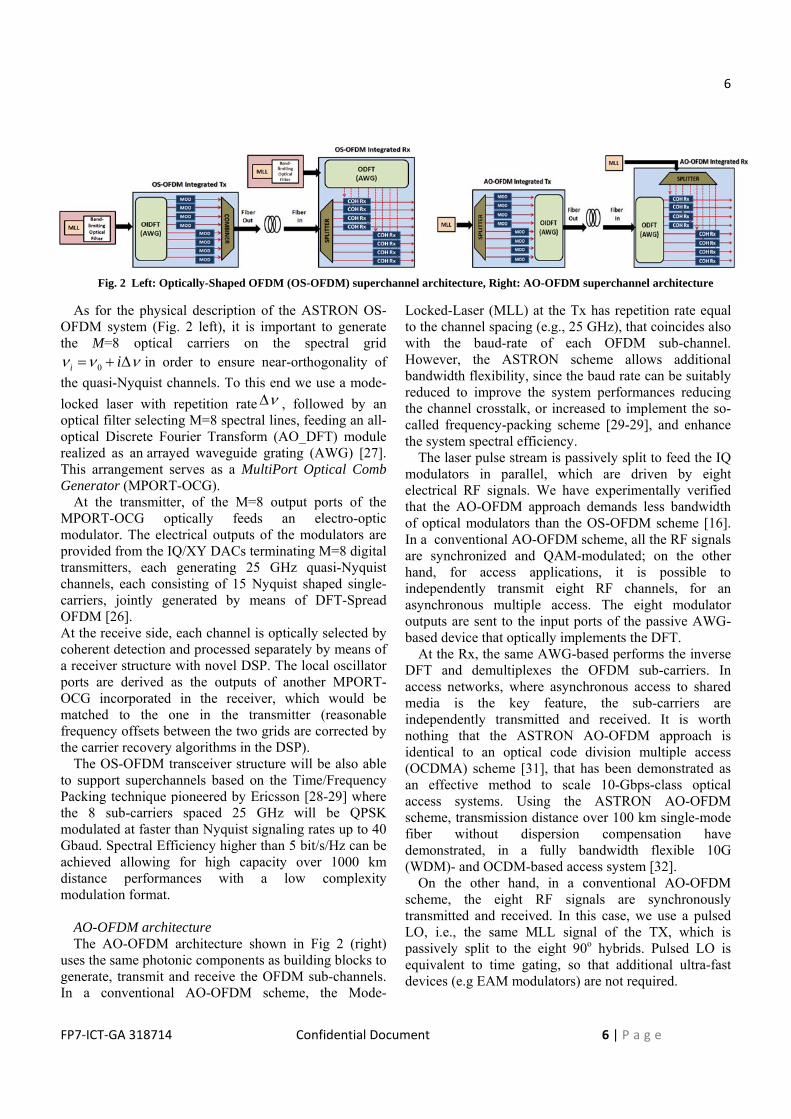
Fig. 2 Left: Optically-Shaped OFDM (OS-OFDM) superchannel architecture, Right: AO-OFDM superchannel architecture
As for the physical description of the ASTRON OS-OFDM system (Fig. 2 left), it is important to generate the M=8 optical carriers on the spectral grid
0i iν ν ν= + Δ in order to ensure near-orthogonality of the quasi-Nyquist channels. To this end we use a mode-locked laser with repetition rate νΔ , followed by an optical filter selecting M=8 spectral lines, feeding an all-optical Discrete Fourier Transform (AO_DFT) module realized as an arrayed waveguide grating (AWG) [27]. This arrangement serves as a MultiPort Optical Comb Generator (MPORT-OCG).
At the transmitter, of the M=8 output ports of the MPORT-OCG optically feeds an electro-optic modulator. The electrical outputs of the modulators are provided from the IQ/XY DACs terminating M=8 digital transmitters, each generating 25 GHz quasi-Nyquist channels, each consisting of 15 Nyquist shaped single-carriers, jointly generated by means of DFT-Spread OFDM [26]. At the receive side, each channel is optically selected by coherent detection and processed separately by means of a receiver structure with novel DSP. The local oscillator ports are derived as the outputs of another MPORT-OCG incorporated in the receiver, which would be matched to the one in the transmitter (reasonable frequency offsets between the two grids are corrected by the carrier recovery algorithms in the DSP).
The OS-OFDM transceiver structure will be also able to support superchannels based on the Time/Frequency Packing technique pioneered by Ericsson [28-29] where the 8 sub-carriers spaced 25 GHz will be QPSK modulated at faster than Nyquist signaling rates up to 40 Gbaud. Spectral Efficiency higher than 5 bit/s/Hz can be achieved allowing for high capacity over 1000 km distance performances with a low complexity modulation format.
AO-OFDM architecture The AO-OFDM architecture shown in Fig 2 (right)
uses the same photonic components as building blocks to generate, transmit and receive the OFDM sub-channels. In a conventional AO-OFDM scheme, the Mode-
Locked-Laser (MLL) at the Tx has repetition rate equal to the channel spacing (e.g., 25 GHz), that coincides also with the baud-rate of each OFDM sub-channel. However, the ASTRON scheme allows additional bandwidth flexibility, since the baud rate can be suitably reduced to improve the system performances reducing the channel crosstalk, or increased to implement the so-called frequency-packing scheme [29-29], and enhance the system spectral efficiency.
The laser pulse stream is passively split to feed the IQ modulators in parallel, which are driven by eight electrical RF signals. We have experimentally verified that the AO-OFDM approach demands less bandwidth of optical modulators than the OS-OFDM scheme [16]. In a conventional AO-OFDM scheme, all the RF signals are synchronized and QAM-modulated; on the other hand, for access applications, it is possible to independently transmit eight RF channels, for an asynchronous multiple access. The eight modulator outputs are sent to the input ports of the passive AWG-based device that optically implements the DFT.
At the Rx, the same AWG-based performs the inverse DFT and demultiplexes the OFDM sub-carriers. In access networks, where asynchronous access to shared media is the key feature, the sub-carriers are independently transmitted and received. It is worth nothing that the ASTRON AO-OFDM approach is identical to an optical code division multiple access (OCDMA) scheme [31], that has been demonstrated as an effective method to scale 10-Gbps-class optical access systems. Using the ASTRON AO-OFDM scheme, transmission distance over 100 km single-mode fiber without dispersion compensation have demonstrated, in a fully bandwidth flexible 10G (WDM)- and OCDM-based access system [32].
On the other hand, in a conventional AO-OFDM scheme, the eight RF signals are synchronously transmitted and received. In this case, we use a pulsed LO, i.e., the same MLL signal of the TX, which is passively split to the eight 90o hybrids. Pulsed LO is equivalent to time gating, so that additional ultra-fast devices (e.g EAM modulators) are not required.

FP7‐ICT‐GA 318714 Confidential Document 7 | P a g e
7
The following sections provide a detailed description of the photonic building blocks to implement the ASTRON transceiver subsystems.
IV. THE ASTRON INTEGRATED TRANSMITTER The development and fabrication of the novel superchannel transmitter shown in Fig. 3 is based on the application and combination of a monolithic and a hybrid integration technology (“monolithic-on-hybrid”). However a full monolithic integration approach on InP would be the most attractive integration concept to provide such complex transmitter components in a compact design. But monolithic integration of such a large scale PIC is currently still a very ambitious and challenging task. For example, the expected large Tx PIC size and thus high optical loss, the limited InP substrate sizes, waste of valuable InP space to provide purely passive optical functions, optical and electrical RF crosstalk, heat management, and device yield are only a few issues in this context. Thus the monolithic-on-hybrid approach has been chosen for the transmitter fabrication in the ASTRON project.
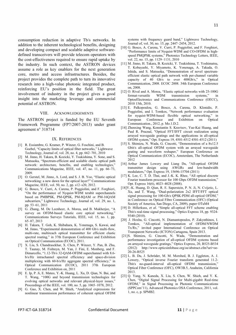
The 8-channel ASTRON transmitter (Fig. 3) consists of a planar optical glass board and two InP-based 4-channel Mach-Zehnder modulator (MZM) IQ photonic integrated circuits (PIC). The board integrates all required passive optical waveguide elements for OFDM/NWDM super channel generation as well as all electrical RF/DC tracks to connect each IQ modulator on the board. The flip-chip ready MZM IQ PICs are mounted up-side down onto the planar glass board by using flip-chip bonding technology and by means of a solder process (Fig. 3). To this aim precise pick-and-place techniques are used for hybrid chip assembly.
The 4-channel MZM IQ PICs will integrate periodically capacitive loaded series push-pull InP travelling wave electrode (TWE) MZ modulators as a basic building block. The vertical and lateral modulator
layout is schematically shown in Fig. 4. Single high performance MZ modulators have been already demonstrated in the past which allow for data rates up to 40 Gb/s and beyond [33-34]. For example, fabricated single 43 Gb/s chirp free modulators can provide < 6 dB optical fiber-to-fiber insertion losses, ≥ 20 dB extinction ratios (ER), and ≤ 2.5 V driving voltages (Vπ) across 40 nm wavelength C-band. The modulator architecture is based on a deeply etched multiple quantum well (MQW) ridge waveguide structure fabricated on a semi-insulating InP:Fe substrate, which is beneficial in terms of performance, footprint, and yield. Standard optical waveguide couplers are used for light separation and coupling in the particular MZ modulator and IQ sections (child, parent). All input and output waveguides are integrated with a spot size converter (SSC) in order to guarantee low loss optical coupling between the different waveguides on chip and transmitter board. Phase sections and monitor photodiodes are integrated on IQ MZM PICs for phase adjustments and calibration/monitoring purposes. In order to achieve high transmission capacity, the integration of capacity-loaded electrical traveling wave electrodes in combination with electrical ground-signal-ground (GSG) and ground-signal (GS) RF transmission lines on the PICs is indispensable.
In order to facilitate the hybrid assembly of the large InP MZM IQ PICs onto the glass motherboard (Fig. 5), specific features have to be integrated on chip level ( e.g. cleave initiators for precise chip cleaving, stand-off pillars for vertical waveguide alignment, and solder bump pads for flip-chip bonding). Moreover, precisely etched deep cavities and stand-off pillars are required on board level for precise chip placement and vertical chip-
Fig. 3 Schematic of the ASTRON transmitter integrated board. Two flip-chip ready InP-based 4-channel MZM IQ PICs (left) are assembled onto the glass board by utilizing flip-chip bonding technology.
Fig. 4 Schematic of the spot-size converter (SSC) integrated TWE MZ modulator which represents the core piece in the 4-channel IQ MZ modulator PIC architectures.
FP7‐ICT‐GA 318714 Confidential Document 8 | P a g e
8
to-board waveguide alignment, respectively. Obviously, the optical interface between board and chip has to be almost ideal in terms of edge steepness and surface roughness.
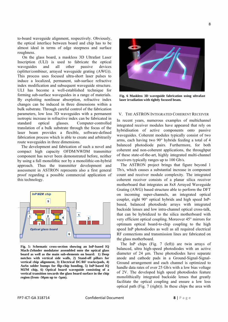
On the glass board, a maskless 3D Ultrafast Laser Inscription (ULI) is used to fabricate the optical waveguides and all other passive devices (splitter/combiner, arrayed waveguide grating (AWG)). This process uses focused ultra-short laser pulses to induce a localized, permanent, sub-surface refractive index modification and subsequent waveguide structure. ULI has become a well-established technique for forming sub-surface waveguides in a range of materials. By exploiting nonlinear absorption, refractive index changes can be induced in three dimensions within a bulk substrate. Through careful control of the fabrication parameters, low loss 3D waveguides with a permanent isotropic increase in refractive index can be fabricated in standard optical glasses. Computer-controlled translation of a bulk substrate through the focus of the laser beam provides a flexible, software-defined fabrication process which is able to create and arbitrarily route waveguides in three dimensions.
The development and fabrication of such a novel and compact high capacity OFDM/NWDM transmitter component has never been demonstrated before, neither by using a full monolithic nor by a monolithic-on-hybrid approach. Thus the transmitter development and assessment in ASTRON represents also a first general proof regarding a possible commercial application of this technology.
V. THE ASTRON INTEGRATED COHERENT RECEIVER In recent years, numerous examples of multichannel integrated receiver modules have appeared that rely on hybridisation of active components onto passive waveguides. Coherent modules typically consist of two arms, each having two 90° hybrids feeding a total of 4 balanced photodiode pairs. Furthermore, for both coherent and non-coherent applications, the throughput of these state-of-the-art, highly integrated multi-channel receivers typically ranges up to 100 Gb/s.
The ASTRON project brings that figure beyond 1 Tb/s, which causes a substantial increase in component count and receiver module complexity. The integrated coherent receiver consists of a planar silica receiver motherboard that integrates an 8x8 Arrayed Waveguide Grating (AWG) based structure able to perform the DFT on incoming super-channels, an integrated optical coupler, eight 90° optical hybrids and high speed InP-based, balanced photodiode arrays with integrated backside lenses and low intra-channel optical cross-talk, that can be hybridized to the silica motherboard with very efficient optical coupling. Moreover 45° mirrors for optimum optical board-to-chip coupling to the high speed InP photodiodes as well as all required electrical RF connections and transmission lines are fabricated on the glass motherboard.
The InP chips (Fig. 7 (left)) are twin arrays of balanced, ultra high-speed photodiodes with an active diameter of 24 μm. These photodiodes have separate anode and cathode pads in a Ground-Signal-Signal-Ground arrangement and each channel is optimized to handle data rates of over 25 Gb/s with a low bias voltage of 2V. The developed high speed photodiodes feature monolithically integrated backside lenses that greatly facilitate the optical coupling and ensure a low loss optical path (Fig. 7 (right)). In these chips the area with
Fig. 6 Maskless 3D waveguide fabrication using ultrafast laser irradiation with tightly focused beam.
Fig. 5: Schematic cross-section showing an InP-based IQ Mach-Zehnder modulator assembled onto the optical glass board as well as the main sub-elements on board: 1) Deep notches with vertical side walls, 2) Stand-off pillars for vertical chip alignment, 3) Electrical DC/RF tracks/pads, 4) AuSn solder bumps for flip-chip bonding, 5) InP-based IQ MZM chip, 6) Optical board waveguide consisting of a vertical transition towards the glass board surface in the chip region (from -50µm up to -5µm).

FP7‐ICT‐GA 318714 Confidential Document 9 | P a g e
9
maximum responsivity is about a factor of three larger for the photodiode with integrated backside lens compared to a photodiode with a conventional flat entry, which gives a significant advantage in terms of optical alignment.
The hybrid assembly of the photodiode chips onto the silica Rx motherboard is performed by a solder process. Therefore the chips feature alignment marks and contact pads on the chip topside and solderable support pads on the backside. The hybrid assembly through a soldering process requires a precise handling of the photodiode to place it with the necessary accuracy onto the destination platform. Therefore a pick-up tool with the appropriate size to fit to the geometry of the photodiode is used. The photodiodes are assembled onto the motherboard with the lens side facing down. The light out of the board silica waveguides is coupled into the photodiode lens with a monolithic 45° mirror structure (Fig. 8). The light beam is focused by the lens, travels through the transparent substrate and reaches the active area where it is effectively absorbed and converted into an electrical current. Besides the mirror structures, all passive structures (e.g. optical waveguides, optical splitter, AWG, 900 hybrids) are fabricated using the same 3D laser inscription described in the previous section. Especially for the 900 hybrids, each one is carefully trimmed, tested and if necessary, re-trimmed in order to tune these to an exact quadrature.
VI. DIGITAL SIGNAL PROCESSING Software defined optical transceivers offer flexibility in channel coding, modulation, and the number of sub-carriers per wavelength. Modulation format and coding levels are flexible and controlled by software; adjusting
the number of bits per symbol, choosing the right modulation format and optimising the filter bandwidths allows throughput to be maximized for a given set of link parameters, including link length, amplifier noise figures, dispersion and fibre nonlinearity. Reprogrammable DSP will allow optimum network utilization [35] with respect to applications, channel requirements and quality of service. For example, the signal bandwidth can be varied, enabling networks based on flexible WDM grids, and allowing more efficient use of resources.
To enable future ultra-high capacity flexible networks, one major objective is to extend the transmission reach and spectral efficiency of OFDM super-channels well beyond the state-of-the-art by digitally mitigating all optical channel impairments. Sub-banded DSP with under-decimated filter banks is a recent DSP HW architecture whereby the bandwidth of the optical channel is digitally partitioned into multiple spectrally disjoint sub-bands to be processed in parallel [36-38]. The resulting optical receiver ASICs are applicable to long-haul and metro photonic communication and may provide substantial energy efficiency savings of 30%-50% in the power consumption of the DSP section. Moreover, as the processing is structured in multiple independent sub-bands (e.g., 15 sub-bands of ~1.7 GHz each), the performance of the multiple parallel sub-band receivers exceeds that of a reference full band 25 GHz conventional Rx which processes the full 25 GHz wide spectrum at once.
We have conceived [36] a twice under-decimated (2xUD) filter bank DSP structure enabling the partitioning into multiple sub-band with high computational efficiency. The 2xUD FB generates 16 twice-oversampled sub-bands (one sub-band is dedicated to the ADC transition) such that the 25 GHz bandwidth is sliced into 15 sub-bands each of 1.66 GHz, twice over-sampled at 3.33 GS/s. The digitally sub-banded architecture is natural to realize in the context of coherent OFDM and DFT-S OFDM [26], since the sub-band partitioning of an OFDM signal by the filter bank results in multiple independent narrower-band OFDM signals (Fig.2(left)). Each of the sub-bands is then detected by separate sub-band OFDM receivers. We further adapted the 2xUD filter-bank to Multi-Sub-Band (MSB) OFDM and DFT-spread OFDM receivers (Fig. 2 (right)), detailing the signal processing chain through the corresponding sub-band processors. The Chromatic
Fig. 8 Light reflected upwards by a 450 mirror. Visible on a silicon CCD camera
Fig. 7 Photographic images of the PD chip topside (left) and backside with integrated lens (right)

FP7‐ICT‐GA 318714 Confidential Document 10 | P a g e
10
Dispersion (CD), Fine Timing Offset (FTO) and Polarization Mode Dispersion (PMD) compensation functions are degenerated to memoryless single-tap equalization; the full DSP chain comprises compensating modules for IQ-imbalance compensation, Carrier-Frequency-Offset (CFO), Course Timing Offset, FFT+two-fold decimation, Polarization Demux, optional DFT-despreading, Phase Recovery+slicing (using Multi Symbol Delay Detection).
We briefly address the root causes of sub-banded performance improvement and the resulting improved characteristics of adaptive acquisition and tracking under the sub-banded paradigm. In terms of DSP hardware architecture, digital sub-banding amounts to an alternative mode of parallelizing the signal processing task to multiple slower processors, whereby the parallelization is performed in the frequency-domain (FD) rather than in the time-domain (TD). FD
parallelization of the DSP processing is especially suited to the long-haul optical fiber channel, the reason being that chromatic dispersion grows with bandwidth squared and PMD also increases with bandwidth, hence our "divide&conquer" approach, partitioning the processing into multiple frequency-domain sub-bands, radically simplifies the filters length, hence real-time computational load is reduced.
Sub-banding should further improve robustness and adaptability in the “control path”. In a full-band Rx, channel estimation and adaptive tracking generally take a major toll on overall complexity and performance. Sub-banding features the frequency-flat sub-banding advantage, attaining rapid and accurate convergence, yielding fast optical channel acquisition and tracking. The resulting receiver ASICs are estimated to be a factor of approximately two less complex in their DSP section in comparison to conventional receiver ASICs. Additional useful strategies enabled by the sub-banding paradigm are: (i): sleep-mode selectively turning sub-bands on and off for energy-efficiency. (ii): Software defined transceivers over flexi-grid variable-channel formation by aggregating sub-bands even across channel boundaries. (iii): Efficient photonic switching at the physical layer, based on digital cross-connects with high-granularity (down to sub-bands) for highly efficient networking. (iv): the potential for sub-banded spatial-division multiplexing equalization.
VII. IMPACT The ASTRON transceiver architecture relies on
leading edge technology providing important contributions beyond the state-of-the-art with respect to photonic technologies, yet it also provides a favorable ground for future technologies on the future network as a whole. The project aspires to contribute to communications networks by increasing the transparency, the information throughput, and the power
1M −
( )H zβ
12M↓
12M↓
12M↓
β
# β
Fig. 10 Top: Novel sub-banded reception in an OFDM link using a conventional OFDM Tx. Bottom: Overall digitally sub-banded Rx.
Xτ
Yτ
Fig. 9 Sub-band (DFT-S) OFDM Rx, detailing the full processing chain.
FP7‐ICT‐GA 318714 Confidential Document 11 | P a g e
11
consumption reduction in adaptive Tb/s networks. In addition to the inherent technological benefits, designing and developing compact and scalable adaptive software-defined transceivers will provide telecom operators with the cost-effectiveness required to ensure rapid uptake by the industry. In such context, the ASTRON devices assume a role as key enablers for the next generation core, metro and access infrastructures. Besides, the project provides the complete path to turn its innovative research into a high-value photonic integrated product, reinforcing EU’s position in the field. The great involvement of industry in the project gives a good insight into the marketing leverage and commercial potential of ASTRON.
VIII. ACKNOWLEDGEMENTS The ASTRON project is funded by the EU Seventh Framework Programme (FP7/2007-2013) under grant agreement n° 318714
IX. REFERENCES [1] R. Essiambre, G. Kramer, P. Winzer, G. Foschini, and B.
Goebel, “Capacity limits of optical fiber networks,” Lightwave Technology, Journal of, vol. 28, no. 4, pp. 662–701, 2010
[2] M. Jinno, H. Takara, B. Kozicki, Y. Tsukishima, Y. Sone, and S. Matsuoka, “Spectrum-efficient and scalable elastic optical path network: architecture, benefits, and enabling technologies,” Communications Magazine, IEEE, vol. 47, no. 11, pp. 66–73, 2009.
[3] O. Gerstel, M. Jinno, A. Lord, and S. J. B. Yoo, “Elastic optical networking: a new dawn for the optical layer?” Communications Magazine, IEEE, vol. 50, no. 2, pp. s12–s20, 2012.
[4] G. Bosco, V. Curri, A. Carena, P. Poggiolini, and F. Forghieri, “On the performance of Nyquist-WDM terabit superchannels based on PMBPSK, PM-QPSK, PM-8QAM or PM-16QAM subcarriers,” Lightwave Technology, Journal of, vol. 29, no. 1, pp. 53–61, 2011
[5] G. Zhang, M. De Leenheer, A. Morea, and B. Mukherjee, “A survey on OFDM-based elastic core optical networking,” Communications Surveys Tutorials, IEEE, vol. 15, no. 1, pp. 65–87, 2013
[6] H. Takara, T. Goh, K. Shibahara, K. Yonenaga, S. Kawai, and M. Jinno, “Experimental demonstration of 400 Gb/s multi-flow, multi-rate, multireach optical transmitter for efficient elastic spectral routing,” in 37th European Conference and Exhibition on Optical Communication (ECOC), 2011.
[7] X. Liu, S. Chandrasekhar, X. Chen, P. Winzer, Y. Pan, B. Zhu, T. Taunay, M. Fishteyn, M. Yan, J. Fini, E. Monberg, and F. Dimarcello, “1.12-Tb/s 32-QAM-OFDM superchannel with 8.6-b/s/Hz intrachannel spectral efficiency and space-division multiplexing with 60-b/s/Hz aggregate spectral efficiency,” in Optical Communication (ECOC), 2011 37th European Conference and Exhibition on, 2011
[8] E. Ip, P. Ji, E. Mateo, Y.-K. Huang, L. Xu, D. Qian, N. Bai, and T. Wang, “100G and beyond transmission technologies for evolving optical networks and relevant physical-layer issues,” Proceedings of the IEEE, vol. 100, no. 5, pp. 1065–1078, 2012.
[9] G. Gao, X. Chen, and W. Shieh, “Analytical expressions for nonlinear transmission performance of coherent optical OFDM
systems with frequency guard band,” Lightwave Technology, Journal of, vol. 30, no. 15, pp. 2447–2454, 2012.
[10] G. Bosco, A. Carena, V. Curri, P. Poggiolini, and F. Forghieri, “Performance limits of Nyquist-WDM and CO-OFDM in high-speed PMQPSK systems,” Photonics Technology Letters, IEEE, vol. 22, no. 15, pp. 1129–1131, 2010
[11] M. Jinno, H. Takara, B. Kozicki, Y. Tsukishima, T. Yoshimatsu, T. Kobayashi, Y. Miyamoto, K. Yonenaga, A. Takada, O. Ishida, and S. Matsuoka, “Demonstration of novel spectrum-efficient elastic optical path network with per-channel variable capacity of 40 Gb/s to over 400Gb/s,” in Optical Communication, 2008. ECOC 2008. 34th European Conference on, 2008.
[12] O. Rival and A. Morea, “Elastic optical networks with 25-100G format-versatile WDM transmission systems,” in OptoeElectronics and Communications Conference (OECC), 2010 15th, 2010.
[13] E. Palkopoulou, G. Bosco, A. Carena, D. Klonidis, P. Poggiolini, and I. Tomkos, “Network performance evaluation for nyquist-WDM-based flexible optical networking,” in European Conference and Exhibition on Optical Communication., 2012, p. Mo.1.D.2.
[14] Zhenxing Wang, Konstantin S. Kravtsov, Yue-Kai Huang, and Paul R. Prucnal, "Optical FFT/IFFT circuit realization using arrayed waveguide gratings and the applications in all-optical OFDM system," Opt. Express 19, 4501-4512 4501-4512 (2011)
[15] S. Shimizu, N. Wada, G. Cincotti, “Demonstration of a 8x12.5 Gbit/s all-optical OFDM system with an arrayed waveguide grating and waveform reshaper,” European Conference on Optical Communication (ECOC), Amsterdam, The Netherlands 2012
[16] Arthur James Lowery and Liang Du, "All-optical OFDM transmitter design using AWGRs and low-bandwidth modulators," Opt. Express 19, 15696-15704 (2011)
[17] K. Lee, C. T. D. Thai, and J.-K. K. Rhee, “All optical discrete Fourier transform processor for 100 Gbps OFDM transmission,” Opt. Express 16(6), 4023–4028 (2008).
[18]Y.-K. Huang, D. Qian, R. E. Saperstein, P. N. Ji, N. Cvijetic, L. Xu, and T. Wang, “Dual-polarization 2x2 IFFT/FFT optical signal processing for 100-Gb/s QPSK-PDM all-optical OFDM,” in Conference on Optical Fibre Communication (OFC) (Optical Society of America, San Diego, CA, 2009), paper OTuM4
[19] D. Hillerkuss, et al. “Simple all-optical FFT scheme enabling Tbit/s real-time signal processing,” Optics Express 18, pp. 9324-9340 (2010).
[20] J. Hoxha, G. Cincotti, N. Diamantopoulos, P. Zakynthinos, I. Tomkos, “All-optical implementation of OFDM/NWDM Tx/Rx,” invited paper International Conference on Optical Transparent Networks (ICTON) Cartagena, Spain 2013.
[21] S. Shimizu, G. Cincotti, N. Wada, “Demonstration and performance investigation of all-optical OFDM systems based on arrayed waveguide gratings,” Optics Express, 20, B525-B534 (2012) http://www.opticsinfobase.org/oe/abstract.cfm?uri=oe-20-26-B525
[22] L. B. Du, J. Schröder, M. M. Morshed, B. J. Eggleton, A. J. Lowery, “Optical inverse Fourier transform generated 11.2-Tbit/s no-guard-interval all-optical OFDM transmission,” Optical Fiber Conference (OFC), OW3B.5, Anaheim, California 2013.
[23] Q. Yang, N. Kaneda, X. Liu, S. Chen, W. Shieh, and Y. K. Chen, “Digital Signal Processing for Multi-gigabit Real-time OFDM,” in Signal Processing in Photonic Communications (SPPCom’11), Advanced Photonics OSA Conference, 2011, vol. 1, no. c, p. SPMB2.

FP7‐ICT‐GA 318714 Confidential Document 12 | P a g e
12
[24] J. Du and S. Signell, “Classic OFDM Systems and pulse shaping OFDM / OQAM Systems, KTH - Royal Institute of Technology report,” 2007.
[25] D. Vuletic, W. Lowdermilk, and F. Harris, “Advantage and Implementation Considerations of Shaped OFDM Signals,” in Signals, Systems and Computers, Thirty-Seventh Asilomar Conference, 2003, pp. 683–687.
[26] Y. Tang, W. Shieh, and B. S. Krongold, “DFT-Spread OFDM for Fiber Nonlinearity Mitigation,” IEEE Photon. Technol. Lett., vol. 22, no. 16, pp. 1250–1252, Aug. 2010.
[27] G. Cincotti, “What else can an AWG do”, Optics Express, Volume 20, Issue 26, Page B288, Dec. 2012
[28] L. Poti et al. “Casting 1 Tb/s DP-QPSK Communication into 200 GHz Bandwidth”, ECOC 2012
[29] F. Cavaliere, L. Giorgi and R. Sabella, “Overcoming the challenges of very high-speed optical transmission “, Ericsson Review, Oct 2013
[30] Hillerkuss, D. et al. “Simple all-optical FFT scheme enabling Tbit/s real-time signal processing”, Optics Express 18, 9324-9340 (2010).
[31] X. Wang, N. Wada, N. Kataoka, T. Miyazaki, G. Cincotti and K.-i. Kitayama, '100km field trial of 1.24 Tbit/s, spectral efficient, asynchronous 5 WDM X 25 DPSK-OCDMA using one set of 50X50 ports large scale en/decoder,' postdeadline paper Optical Fibre Communication Conference OFC, Anaheim, California 2007
[32] T. Kodama, Y. Tanaka, S. Yoshima, N. Kataoka, J.-i. Nakagawa, S. Shimizu, N. Wada, and K.-i. Kitayama, “Scaling the system capacity and reach of a 10G-TDM–OCDM-PON system without an en/decoder at an ONU J. Optical Communication Networks, vol. 5, pp. 134-143, 2013.
[33] K. Prosyk et al.: Travelling Wave Mach-Zehnder Modulators, 25th International Conf. on Indium Phosphide and Related Materials (IPRM), 2013, Kobe (Japan), paper M03-1.
[34] K.O. Velthaus, et al: High performance InP-based Mach-Zehnder modulators for 10 to 100 Gb/s optical fiber transmission systems, in Proc. of IPRM 2011, Berlin (Germany), April 2011, paper #Th9.2.1.
[35] C. Glingener, ‘Optical networking trends and evolution’, in Proc. OFC 2011, Paper OThAA1
[36] M. Nazarathy and A. Tolmachev, “Sub-banded DSP architectures based on under-decimated filter-banks for coherent OFDM receivers,” IEEE Signal Process. Mag., no. Special Issue on Advanced DSP and Coding for Multi-Tb/s Optical Transport, 2014.
[37] A. Tolmachev and M. Nazarathy, “Filter-bank based efficient transmission of Reduced-Guard-Interval OFDM,” Opt. Express, vol. 19, no. 26, pp. 370–384, 2011.
[38] K.-P. Ho, “Subband equaliser for chromatic dispersion of optical fibre,” Electron. Lett., vol. 45, no. 24, p. 1224, 2009.