conga-umx6 user's guide - dpie.com · this user’s guide provides information about the...
TRANSCRIPT

Copyright © 2016 congatec AG UMX6m10 1/52
Qseven® conga-UMX6NXP® i.MX6 ARM® Cortex A9 processor with Ultra Low Power Consumption
User’s Guide
Revision 1.0
Copyright © 2016 congatec AG UMX6m10 2/52
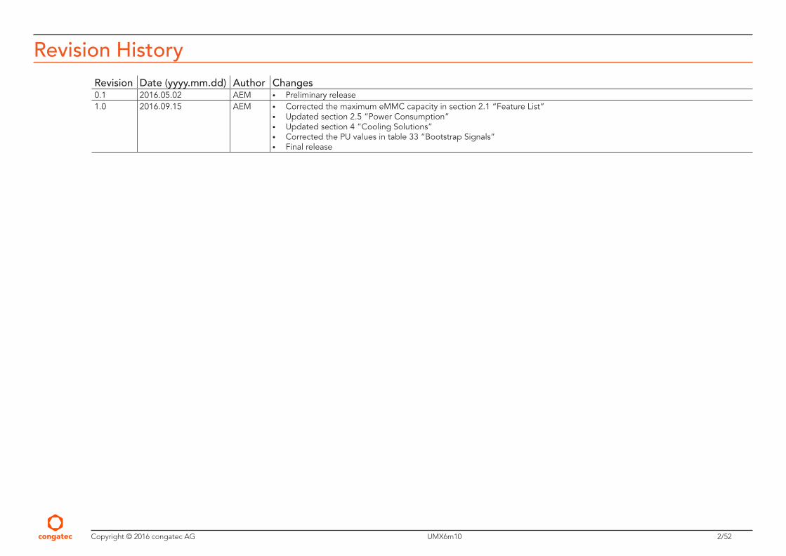
Revision HistoryRevision Date (yyyy.mm.dd) Author Changes0.1 2016.05.02 AEM • Preliminary release1.0 2016.09.15 AEM • Corrected the maximum eMMC capacity in section 2.1 “Feature List”
• Updated section 2.5 “Power Consumption” • Updated section 4 “Cooling Solutions” • Corrected the PU values in table 33 “Bootstrap Signals” • Final release
Copyright © 2016 congatec AG UMX6m10 3/52
PrefaceThis user’s guide provides information about the components, features, connectors and signals available on the conga-UMX6. It is one of four documents that you should refer to when designing an i.MX6 based Qseven® application. The other reference documents that should be used include the following:
Qseven® Design GuideQseven® Specificationi.MX6 Applications Processor Reference Manual (available at www.nxp.com)
The links to these documents can be found on the congatec AG website at www.congatec.com
Disclaimer
The information contained within this user’s guide, including but not limited to any product specification, is subject to change without notice.
congatec AG provides no warranty with regard to this user’s guide or any other information contained herein and hereby expressly disclaims any implied warranties of merchantability or fitness for any particular purpose with regard to any of the foregoing. congatec AG assumes no liability for any damages incurred directly or indirectly from any technical or typographical errors or omissions contained herein or for discrepancies between the product and the user’s guide. In no event shall congatec AG be liable for any incidental, consequential, special, or exemplary damages, whether based on tort, contract or otherwise, arising out of or in connection with this user’s guide or any other information contained herein or the use thereof.
Intended Audience
This user’s guide is intended for technically qualified personnel. It is not intended for general audiences.
Lead-Free Designs (RoHS)
All congatec AG designs are created from lead-free components and are completely RoHS compliant.

Copyright © 2016 congatec AG UMX6m10 4/52
Electrostatic Sensitive Device
All congatec AG products are electrostatic sensitive devices and are packaged accordingly. Do not open or handle a congatec AG product except at an electrostatic-free workstation. Additionally, do not ship or store congatec AG products near strong electrostatic, electromagnetic, magnetic, or radioactive fields unless the device is contained within its original manufacturer’s packaging. Be aware that failure to comply with these guidelines will void the congatec AG Limited Warranty.
Symbols
The following symbols are used in this user’s guide:
Warning
Warnings indicate conditions that, if not observed, can cause personal injury.
Caution
Cautions warn the user about how to prevent damage to hardware or loss of data.
Note
Notes call attention to important information that should be observed.
Copyright Notice
Copyright © 2016, congatec AG. All rights reserved. All text, pictures and graphics are protected by copyrights. No copying is permitted without written permission from congatec AG.
congatec AG has made every attempt to ensure that the information in this document is accurate yet the information contained within is supplied “as-is”.
Trademarks
Product names, logos, brands, and other trademarks featured or referred to within this user’s guide, or the congatec website, are the property of their respective trademark holders. These trademark holders are not affiliated with congatec AG, our products, or our website.
Copyright © 2016 congatec AG UMX6m10 5/52
Warranty
congatec AG makes no representation, warranty or guaranty, express or implied regarding the products except its standard form of limited warranty (“Limited Warranty”) per the terms and conditions of the congatec entity, which the product is delivered from. These terms and conditions can be downloaded from www.congatec.com. congatec AG may in its sole discretion modify its Limited Warranty at any time and from time to time.
The products may include software. Use of the software is subject to the terms and conditions set out in the respective owner’s license agreements, which are available at www.congatec.com and/or upon request.
Beginning on the date of shipment to its direct customer and continuing for the published warranty period, congatec AG represents that the products are new and warrants that each product failing to function properly under normal use, due to a defect in materials or workmanship or due to non conformance to the agreed upon specifications, will be repaired or exchanged, at congatec’s option and expense.
Customer will obtain a Return Material Authorization (“RMA”) number from congatec AG prior to returning the non conforming product freight prepaid. congatec AG will pay for transporting the repaired or exchanged product to the customer.
Repaired, replaced or exchanged product will be warranted for the repair warranty period in effect as of the date the repaired, exchanged or replaced product is shipped by congatec, or the remainder of the original warranty, whichever is longer. This Limited Warranty extends to congatec’s direct customer only and is not assignable or transferable.
Except as set forth in writing in the Limited Warranty, congatec makes no performance representations, warranties, or guarantees, either express or implied, oral or written, with respect to the products, including without limitation any implied warranty (a) of merchantability, (b) of fitness for a particular purpose, or (c) arising from course of performance, course of dealing, or usage of trade.
congatec AG shall in no event be liable to the end user for collateral or consequential damages of any kind. congatec shall not otherwise be liable for loss, damage or expense directly or indirectly arising from the use of the product or from any other cause. The sole and exclusive remedy against congatec, whether a claim sound in contract, warranty, tort or any other legal theory, shall be repair or replacement of the product only.
Certification
congatec AG is certified to DIN EN ISO 9001:2008 standard. CERTIFICATION
ISO 9001
TM

Copyright © 2016 congatec AG UMX6m10 6/52
Technical Support
congatec AG technicians and engineers are committed to providing the best possible technical support for our customers so that our products can be easily used and implemented. We request that you first visit our website at www.congatec.com for the latest documentation, utilities and drivers, which have been made available to assist you. If you still require assistance after visiting our website then contact our technical support department by email at [email protected].
Terminology
Term DescriptionPCI Express (PCIe) Peripheral Component Interface ExpressARM Advanced RISC MachineJTAG Joint Test Action GroupeCSPI Enhanced Configurable Serial Peripheral InterfaceGPIO General Purpose Input OutputRGMII Reduced Gigabit Media Independent InterfaceeMMC Embedded Multi Media CardSDIO Secure Digital Input Output.USB Universal Serial BusSATA Serial AT AttachmentHDA High Definition AudioHDMI High Definition Multimedia InterfaceTMDS Transition Minimized Differential SignalingDVI Digital Visual Interface I²C Bus Inter-Integrated Circuit BusSM Bus System Management Bus SPI Bus Serial Peripheral Interface BusCAN Bus Controller-area networkAMBA Advanced Microcontroller Bus ArchitectureIOMUX Input Output MultiplexerGbE Gigabit EthernetLVDS Low-Voltage Differential Signaling DDC Display Data ChannelN.C. Not connectedN.A. Not availableT.B.D. To be determined
Copyright © 2016 congatec AG UMX6m10 7/52
Contents1 Introduction ............................................................................... 9
2 Specifications ........................................................................... 11
2.1 Feature List .............................................................................. 112.2 Supported Operating Systems ................................................ 122.3 Mechanical Dimensions ........................................................... 122.4 Supply Voltage Standard Power .............................................. 132.4.1 Electrical Characteristics .......................................................... 132.4.2 Rise Time ................................................................................. 132.5 Power Consumption ................................................................ 142.6 Supply Voltage Battery Power ................................................. 162.6.1 CMOS Battery Power Consumption ........................................ 162.7 Environmental Specifications ................................................... 17
3 Block Diagram .......................................................................... 18
4 Cooling Solutions ..................................................................... 19
4.1 Heatspreader Dimensions ........................................................ 19
5 Connector Subsystems ............................................................ 22
5.1 PCI Express™ ........................................................................... 225.2 UART ........................................................................................ 225.3 Gigabit Ethernet ...................................................................... 235.4 SATA ........................................................................................ 235.5 USB 2.0 .................................................................................... 235.6 SD/SDIO/MMC ........................................................................ 245.7 HDA/I2S/AC’97 ........................................................................ 245.8 LVDS ......................................................................................... 245.9 HDMI ........................................................................................ 255.10 GPIO ........................................................................................ 255.11 SPI ............................................................................................ 255.12 CAN Bus .................................................................................. 255.13 Manufacturing/JTAG Interface ................................................. 265.14 Power Control .......................................................................... 26
5.15 Power Management ................................................................. 285.16 Watchdog ................................................................................ 285.17 I2C Bus ..................................................................................... 28
6 Additional Features .................................................................. 29
6.1 High Assurance Boot (HAB) ..................................................... 296.2 Dedicated Hardware Accelerators ........................................... 296.3 Power Management ................................................................. 296.4 Dynamic Voltage and Frequency Scaling ................................ 296.5 Smart Speed Technology ......................................................... 306.6 Suspend Mode ......................................................................... 30
7 conga Tech Notes .................................................................... 31
7.1 ARM Technologies ................................................................... 317.1.1 Media Processing Engine (MPE-NEON) ................................. 317.1.2 Jazelle DBX .............................................................................. 317.1.3 TrustZone ................................................................................. 317.1.4 Floating Point Unit ................................................................... 317.2 NXP® i.MX6 Processor Features ............................................... 327.2.1 Temperature Monitor (TEMPMON) .......................................... 327.3 Thermal Management ............................................................. 327.4 Audio Mux ............................................................................... 337.5 LVDS Bridge ............................................................................. 337.6 USB Port Connections .............................................................. 33
8 Interface - Signal Descriptions and Pinout Tables .................... 35
8.1 Bootstrap Signals ..................................................................... 50
9 Onboard Interfaces and Devices ............................................. 51
9.1 SPI Flash ................................................................................... 519.2 DDR3 Memory ......................................................................... 519.3 eMMC ...................................................................................... 51
10 Industry Specifications ............................................................. 52
Copyright © 2016 congatec AG UMX6m10 8/52
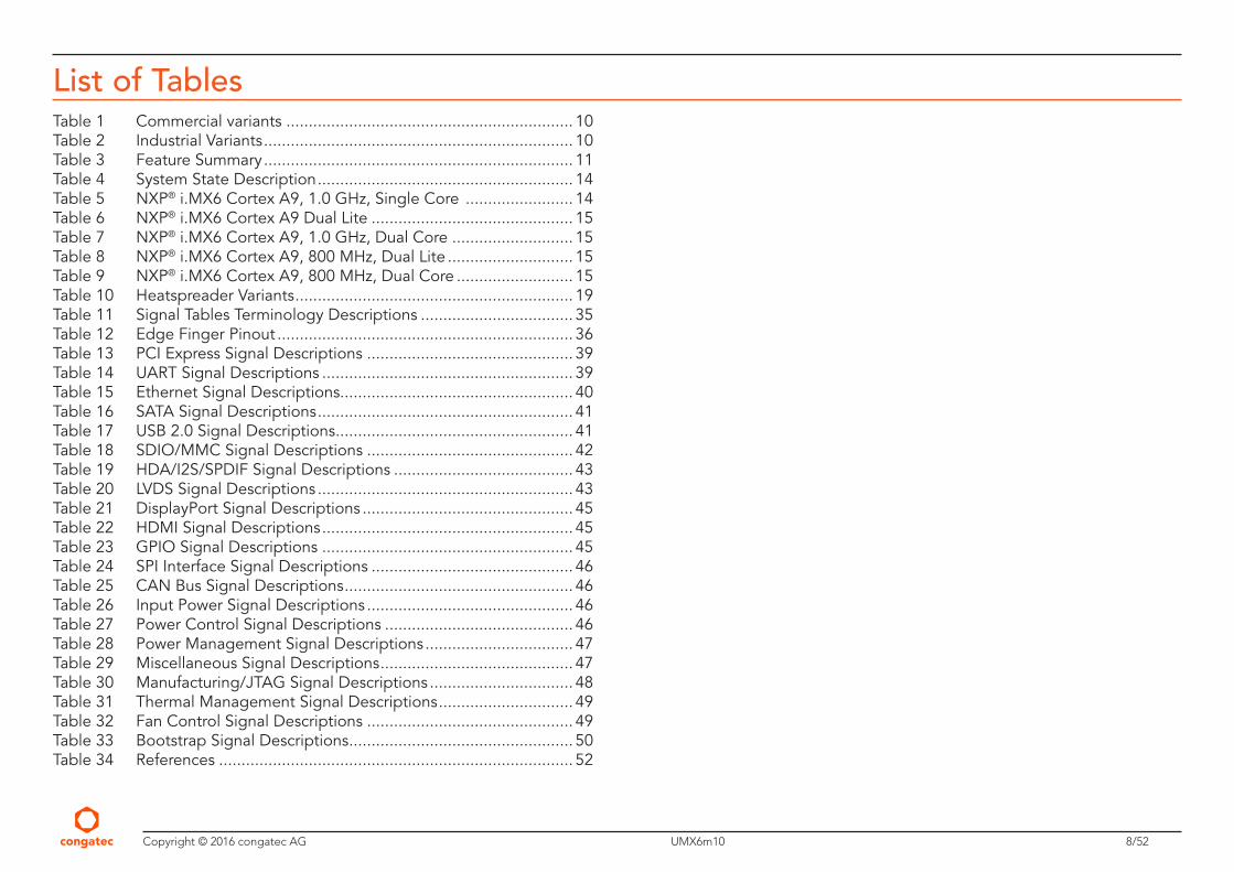
List of TablesTable 1 Commercial variants ................................................................ 10Table 2 Industrial Variants ..................................................................... 10Table 3 Feature Summary ..................................................................... 11Table 4 System State Description ......................................................... 14Table 5 NXP® i.MX6 Cortex A9, 1.0 GHz, Single Core ........................ 14Table 6 NXP® i.MX6 Cortex A9 Dual Lite ............................................. 15Table 7 NXP® i.MX6 Cortex A9, 1.0 GHz, Dual Core ........................... 15Table 8 NXP® i.MX6 Cortex A9, 800 MHz, Dual Lite ............................ 15Table 9 NXP® i.MX6 Cortex A9, 800 MHz, Dual Core .......................... 15Table 10 Heatspreader Variants .............................................................. 19Table 11 Signal Tables Terminology Descriptions .................................. 35Table 12 Edge Finger Pinout .................................................................. 36Table 13 PCI Express Signal Descriptions .............................................. 39Table 14 UART Signal Descriptions ........................................................ 39Table 15 Ethernet Signal Descriptions.................................................... 40Table 16 SATA Signal Descriptions ......................................................... 41Table 17 USB 2.0 Signal Descriptions ..................................................... 41Table 18 SDIO/MMC Signal Descriptions .............................................. 42Table 19 HDA/I2S/SPDIF Signal Descriptions ........................................ 43Table 20 LVDS Signal Descriptions ......................................................... 43Table 21 DisplayPort Signal Descriptions ............................................... 45Table 22 HDMI Signal Descriptions ........................................................ 45Table 23 GPIO Signal Descriptions ........................................................ 45Table 24 SPI Interface Signal Descriptions ............................................. 46Table 25 CAN Bus Signal Descriptions ................................................... 46Table 26 Input Power Signal Descriptions .............................................. 46Table 27 Power Control Signal Descriptions .......................................... 46Table 28 Power Management Signal Descriptions ................................. 47Table 29 Miscellaneous Signal Descriptions ........................................... 47Table 30 Manufacturing/JTAG Signal Descriptions ................................ 48Table 31 Thermal Management Signal Descriptions .............................. 49Table 32 Fan Control Signal Descriptions .............................................. 49Table 33 Bootstrap Signal Descriptions .................................................. 50Table 34 References ............................................................................... 52
Copyright © 2016 congatec AG UMX6m10 9/52
1 Introduction
Qseven® Concept
The Qseven® concept is an off-the-shelf, multi vendor, Single-Board-Computer that integrates all the core components of a common PC and is mounted onto an application specific carrier board. Qseven® modules have a standardized form factor of 70mm x 70mm and a specified pinout based on the high speed MXM system connector. The pinout remains the same regardless of the vendor. The Qseven® module provides the functional requirements for an embedded application. These functions include, but are not limited to graphics, sound, mass storage, network interface and multiple USB ports.
A single ruggedized MXM connector provides the carrier board interface to carry all the I/O signals to and from the Qseven® module. This MXM connector is a well known and proven high speed signal interface connector that is commonly used for high speed PCI Express graphics cards in notebooks.
Carrier board designers can utilize as little or as many of the I/O interfaces as deemed necessary. The carrier board can therefore provide all the interface connectors required to attach the system to the application specific peripherals. This versatility allows the designer to create a dense and optimized package, which results in a more reliable product while simplifying system integration.
The Qseven® evaluation carrier board provides carrier board designers with a reference design platform and the opportunity to test all the Qseven® I/O interfaces available and then choose the interfaces that suit their application. Qseven® applications are scalable; therefore, once a carrier board has been created, you can easily diversify your product range by using a different performance class Qseven® modules. Simply unplug one module and replace it with another; no need to redesign the carrier board.
This document describes the features available on the conga-UMX6, a congatec module based on NXP’s i.MX6 ARM Cortex A9 processor.
Note
The conga-UMX6 design is based on the Qseven specification 2.0 and the Qseven Specification 2.0 Errata.
Copyright © 2016 congatec AG UMX6m10 10/52
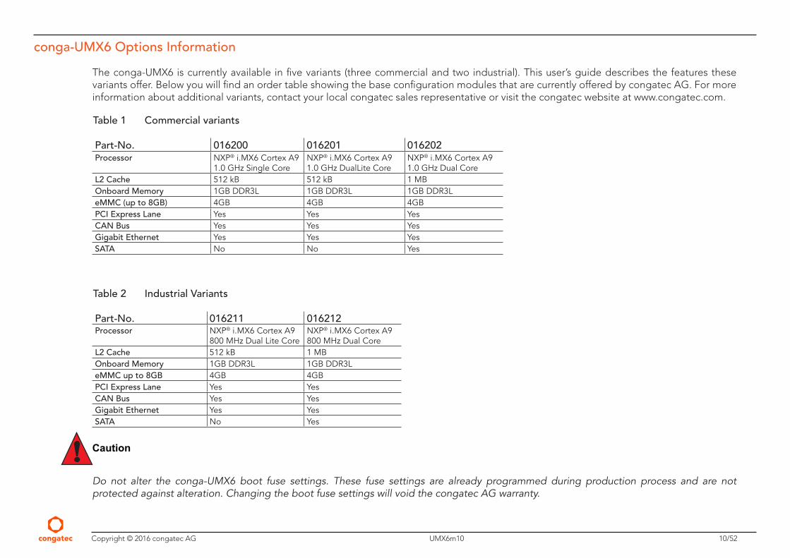
conga-UMX6 Options Information
The conga-UMX6 is currently available in five variants (three commercial and two industrial). This user’s guide describes the features these variants offer. Below you will find an order table showing the base configuration modules that are currently offered by congatec AG. For more information about additional variants, contact your local congatec sales representative or visit the congatec website at www.congatec.com.
Table 1 Commercial variants
Part-No. 016200 016201 016202Processor NXP® i.MX6 Cortex A9
1.0 GHz Single CoreNXP® i.MX6 Cortex A9 1.0 GHz DualLite Core
NXP® i.MX6 Cortex A9 1.0 GHz Dual Core
L2 Cache 512 kB 512 kB 1 MBOnboard Memory 1GB DDR3L 1GB DDR3L 1GB DDR3LeMMC (up to 8GB) 4GB 4GB 4GBPCI Express Lane Yes Yes YesCAN Bus Yes Yes YesGigabit Ethernet Yes Yes YesSATA No No Yes
Table 2 Industrial Variants
Part-No. 016211 016212Processor NXP® i.MX6 Cortex A9
800 MHz Dual Lite CoreNXP® i.MX6 Cortex A9 800 MHz Dual Core
L2 Cache 512 kB 1 MBOnboard Memory 1GB DDR3L 1GB DDR3LeMMC up to 8GB 4GB 4GBPCI Express Lane Yes YesCAN Bus Yes YesGigabit Ethernet Yes YesSATA No Yes
Caution
Do not alter the conga-UMX6 boot fuse settings. These fuse settings are already programmed during production process and are not protected against alteration. Changing the boot fuse settings will void the congatec AG warranty.
Copyright © 2016 congatec AG UMX6m10 11/52
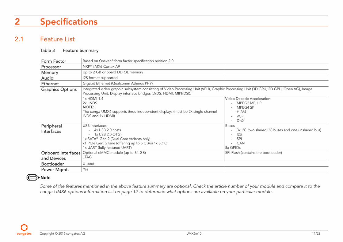
2 Specifications
2.1 Feature List
Table 3 Feature Summary
Form Factor Based on Qseven® form factor specification revision 2.0
Processor NXP® i.MX6 Cortex A9
Memory Up to 2 GB onboard DDR3L memory
Audio I2S format supported
Ethernet Gigabit Ethernet (Qualcomm Atheros PHY)
Graphics Options Integrated video graphic subsystem consisting of Video Processing Unit (VPU), Graphic Processing Unit (3D GPU, 2D GPU, Open VG), Image Processing Unit, Display interface bridges (LVDS, HDMI, MIPI/DSI).1x HDMI 1.42x LVDSNOTE: The conga-UMX6 supports three independent displays (must be 2x single channel LVDS and 1x HDMI)
Video Decode Acceleration: - MPEG2 MP, HP - MPEG4 SP - H.264 - VC-1 - DivX
Peripheral Interfaces
USB Interfaces - 4x USB 2.0 hosts - 1x USB 2.0 OTG)
1x SATA® Gen 2 (Dual Core variants only)x1 PCIe Gen. 2 lane (offering up to 5 GB/s) 1x SDIO1x UART (fully featured UART)
Buses - 3x I²C (two shared I²C buses and one unshared bus) - I2S - SPI - CAN
8x GPIOs
Onboard Interfaces and Devices
Optional eMMC module (up to 64 GB)JTAG
SPI Flash (contains the bootloader)
Bootloader U-boot
Power Mgmt. Yes
Note
Some of the features mentioned in the above feature summary are optional. Check the article number of your module and compare it to the conga-UMX6 options information list on page 12 to determine what options are available on your particular module.

Copyright © 2016 congatec AG UMX6m10 12/52
2.2 Supported Operating Systems
The conga-UMX6 supports the following Operating Systems.
• Microsoft® Windows® Embedded Compact 7
• Microsoft® Windows® Embedded Compact 2013
• Android
• Linux
2.3 Mechanical Dimensions • 40.0 mm x 70.0 mm
• The Qseven™ module, including the heatspreader plate, PCB thickness and bottom components, is up to approximately 12 mm thick.
Heatspeader
Qseven Module PCB
Carrier Board PCB
Dimension is dependenton connector height used
Dimension is dependenton connector height used
All measurements are in millimetersAll dimensions without tolerance ±0.2mm
Rear View of Qseven Module
2.50
1.20 ±0.1
5.50 8.00

Copyright © 2016 congatec AG UMX6m10 13/52
2.4 Supply Voltage Standard Power • 5V DC ± 5%
The dynamic range shall not exceed the static range.
2.4.1 Electrical Characteristics
Characteristics Min. Typ. Max. Units Comment5V Voltage ± 5% 4.75 5.00 5.25 Vdc
Ripple - - ± 50 mVPP 0-20 MHzCurrent
5V_SB Voltage ± 5% 4.75 5.00 5.25 VdcRipple ± 50 mVPP
2.4.2 Rise Time
The input voltages shall rise from 10 percent of nominal to 90 percent of nominal at a minimum slope of 250 V/s. The smooth turn-on requires that during the 10 percent to 90 percent portion of the rise time, the slope of the turn-on waveform must be positive.
Note
For information about the input power sequencing of the Qseven® module, refer to the Qseven® specification.
Nominal Static Range
Dynamic Range
Absolute Minimum
Absolute Maximum5.25V
4.75V
5V
5.05V
4.95V
Copyright © 2016 congatec AG UMX6m10 14/52
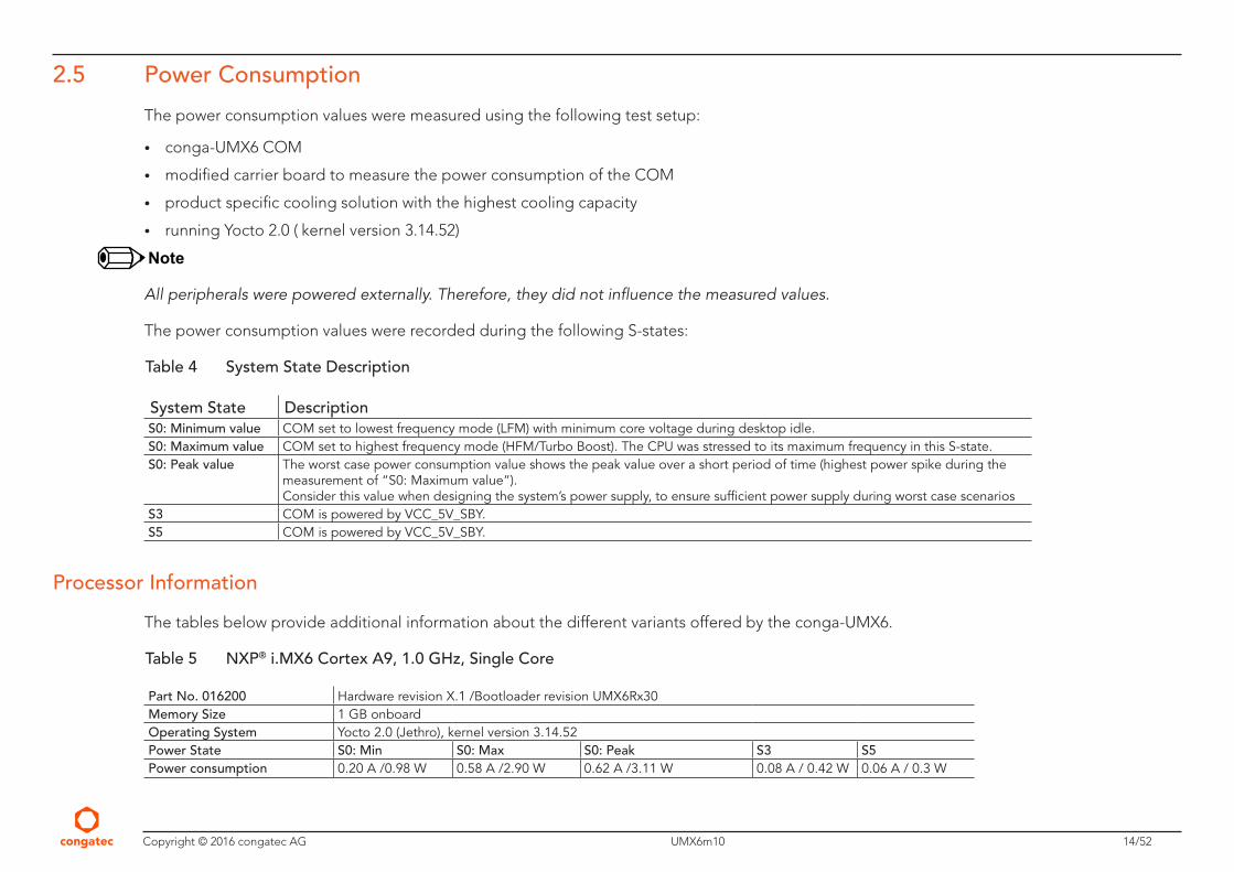
2.5 Power Consumption
The power consumption values were measured using the following test setup:
• conga-UMX6 COM
• modified carrier board to measure the power consumption of the COM
• product specific cooling solution with the highest cooling capacity
• running Yocto 2.0 ( kernel version 3.14.52)
Note
All peripherals were powered externally. Therefore, they did not influence the measured values.
The power consumption values were recorded during the following S-states:
Table 4 System State Description
System State DescriptionS0: Minimum value COM set to lowest frequency mode (LFM) with minimum core voltage during desktop idle. S0: Maximum value COM set to highest frequency mode (HFM/Turbo Boost). The CPU was stressed to its maximum frequency in this S-state.S0: Peak value The worst case power consumption value shows the peak value over a short period of time (highest power spike during the
measurement of “S0: Maximum value”). Consider this value when designing the system’s power supply, to ensure sufficient power supply during worst case scenarios
S3 COM is powered by VCC_5V_SBY.S5 COM is powered by VCC_5V_SBY.
Processor Information
The tables below provide additional information about the different variants offered by the conga-UMX6.
Table 5 NXP® i.MX6 Cortex A9, 1.0 GHz, Single Core
Part No. 016200 Hardware revision X.1 /Bootloader revision UMX6Rx30Memory Size 1 GB onboardOperating System Yocto 2.0 (Jethro), kernel version 3.14.52Power State S0: Min S0: Max S0: Peak S3 S5Power consumption 0.20 A /0.98 W 0.58 A /2.90 W 0.62 A /3.11 W 0.08 A / 0.42 W 0.06 A / 0.3 W

Copyright © 2016 congatec AG UMX6m10 15/52
Table 6 NXP® i.MX6 Cortex A9 Dual Lite
Part No. 016201 Hardware revision X.1 /Bootloader revision UMX6Rx30Memory Size 1 GB onboardOperating System Yocto 2.0 (Jethro), kernel version 3.14.52Power State S0: Min S0: Max S0: Peak S3 S5Power Consumption 0.21 A / 1.05 W 0.86 A / 4.28 W 0.9 A / 4.5 W 0.08 A / 0.42 W 0.06 A / 0.31 W
Table 7 NXP® i.MX6 Cortex A9, 1.0 GHz, Dual Core
Part No. 016202 Hardware revision X.1 /Bootloader revision UMX6Rx30Memory Size 1 GB onboardOperating System Yocto 2.0 (Jethro), kernel version 3.14.52Power State S0: Min S0: Max S0: Peak S3 S5Power consumption 0.24 A / 1.18 W 0.99 A / 4.96 W 1.10 A / 5.51 W 0.08 A / 0.42 W 0.05 A /0.27 W
Table 8 NXP® i.MX6 Cortex A9, 800 MHz, Dual Lite
Part No. 016211 Hardware revision X.1 /Bootloader revision UMX6Rx30Memory Size 1 GB onboardOperating System Yocto 2.0 (Jethro), kernel version 3.14.52Power State S0: Min S0: Max S0: Peak S3 S5Power consumption 0.19 A / 0.95 W 0.71 A / 3.53 W 0.74 A / 3.71 W 0.08 A / 0.42 W 0.06 A / 0.28 W
Table 9 NXP® i.MX6 Cortex A9, 800 MHz, Dual Core
Part No. 016212 Hardware revision X.1 /Bootloader revision UMX6Rx30Memory Size 1 GB onboardOperating System Yocto 2.0 (Jethro), kernel version 3.14.52Power State S0: Min S0: Max S0: Peak S3 S5Power consumption 0.22 A / 1.10 W 0.86 A /4.31 W 0.97 A / 4.85 W 0.09 A / 0.43 W 0.06 A / 0.28 W

Copyright © 2016 congatec AG UMX6m10 16/52
Note
These power consumption values are approximate and only valid for the controlled environment described earlier. The 100 percent workload refers to the CPU workload and not the maximum workload of the complete module. Power consumption results depend on the workload of other components such as graphics engine, memory, etc.
2.6 Supply Voltage Battery Power • 2.0 V - 3.6 V DC
• Typical 3 V DC
2.6.1 CMOS Battery Power Consumption
RTC @ 20ºC Voltage CurrentRTC onboard the conga-UMX6 module 3V DC 3.33 µA
Do not use the above CMOS battery power consumption value to calculate CMOS battery lifetime. Measure the CMOS battery power consumption in your customer specific application in worst case conditions (for example during high temperature and high battery voltage). The self-discharge of the battery must also be considered when determining CMOS battery lifetime. For more information about calculating CMOS battery lifetime refer to application note AN9_RTC_Battery_Lifetime.pdf, which can be found on the congatec AG website at www.congatec.com.
Note
To improve the lifetime of the CMOS battery, congatec implemented an external real time clock onboard the conga-UMX6 module.

Copyright © 2016 congatec AG UMX6m10 17/52
2.7 Environmental Specifications
Temperature Operation: 0° to 60°C Storage: -20° to +80°C (commercial variants)
Temperature Operation: -40° to 85°C Storage: -40° to +85°C (industrial variants)
Humidity Operation: 10% to 90% Storage: 5 % to 95 %
Caution
The above operating temperatures must be strictly adhered to at all times. When using a congatec heatspreader, the maximum operating temperature refers to any measurable spot on the heatspreader’s surface.
Humidity specifications are for non-condensing conditions.
Copyright © 2016 congatec AG UMX6m10 18/52
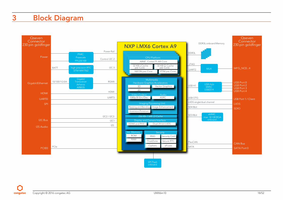
3 Block Diagram
LVDS single/dual channelLVDS
USB OTG USB Port 1 / Client
SD4 8bit SDIO
USB Port 0USB Port 2USB Port 3USB Port 4
FlexCANCAN Bus
SATA
USB H1
JTAG
UART2
DDR3LPower Rail
Control I2C 2
HDMI
FreescalePFUZE100
PMIC
I2S Audio
SD3 8bit
Connector230 pin goldfinger
Gigabit Ethernet
SATA Port 0
I2C Bus
QsevenConnector
230 pin goldfinger
Qseven
UART0
SPI
PCIE0
MFG_NC0...4
Android Buttonsonboard connector
Feature ConnectorMIPI/CMOS camera
SPI Flashonboard
NXP i.MX6 Cortex A9DDR3L onboard Memory
MUX
SMSCUSB2514
USB-Hub
eMMCmax. 32 GB BGA
onboard
Power
MAXIMMAX3232
RS232Debug Port
onboard
AtherosAR8035
TransceiverGigabit
RGMII
HDMI
10/100/1G Eth
I2C1
I2C2 / I2C3
I2S
UART3
PCIe
ARM® Cortex™-A9 Core
32 KB I-Cacheper Core
NEON per Core
32 KB D-Cacheper Core
PTM per Core
CPU Platform
256 KB–1 MB L2-Cache
I2C 3high precision RTCSTM M41T62
BATT
MultimediaHardware Graphics Accelerators
Vector Graphics3D
2D
1080p30 Enc/Dec ASRCVideo Codecs Audio
Imaging Processing Unit
Resizing and Blending
Inversion/Rotation
Image Enhancement
Display and Camera Interface
HDMI and PHY Dual 24-bit LVDS
ROM
RAM
Int. Memory
RNG
TrustZone
Ciphers
Security Cntrl.
Secure RTC
eFuses
Security
Copyright © 2016 congatec AG UMX6m10 19/52
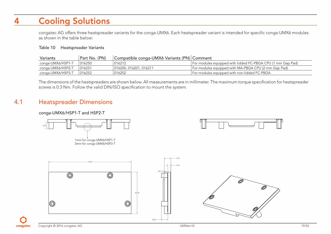
4 Cooling Solutionscongatec AG offers three heatspreader variants for the conga-UMX6. Each heatspreader variant is intended for specific conga-UMX6 modules as shown in the table below:
Table 10 Heatspreader Variants
Variants Part No. (PN) Compatible conga-UMX6 Variants (PN) Commentconga-UMX6/HSP1-T 016250 016212 For modules equipped with lidded FC-PBGA CPU (1 mm Gap Pad)conga-UMX6/HSP2-T 016251 016200, 016201, 016211 For modules equipped with MA-PBGA CPU (2 mm Gap Pad)conga-UMX6/HSP3-T 016252 016202 For modules equipped with non-lidded FC-PBGA
The dimensions of the heatspreaders are shown below. All measurements are in millimeter. The maximum torque specification for heatspreader screws is 0.3 Nm. Follow the valid DIN/ISO specification to mount the system.
4.1 Heatspreader Dimensions
conga-UMX6/HSP1-T and HSP2-T
1mm for conga-UMX6/HSP1-T2mm for conga-UMX6/HSP2-T
Copyright © 2016 congatec AG UMX6m10 20/52
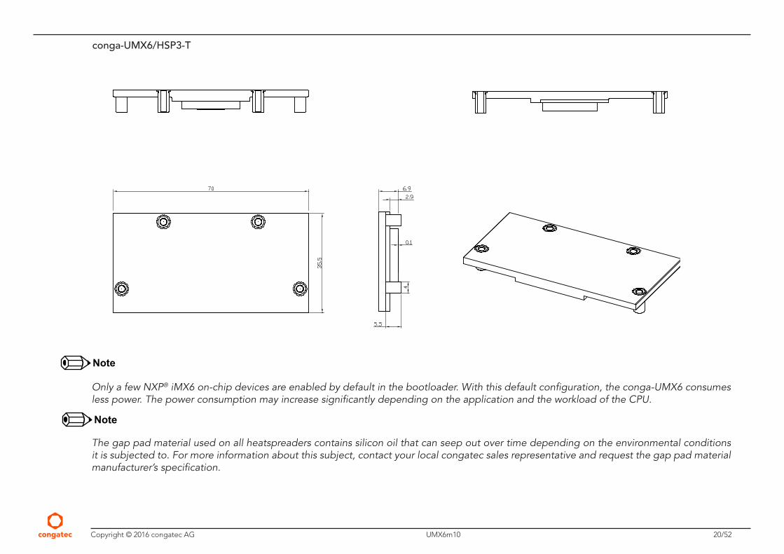
conga-UMX6/HSP3-T
Note
Only a few NXP® iMX6 on-chip devices are enabled by default in the bootloader. With this default configuration, the conga-UMX6 consumes less power. The power consumption may increase significantly depending on the application and the workload of the CPU.
Note
The gap pad material used on all heatspreaders contains silicon oil that can seep out over time depending on the environmental conditions it is subjected to. For more information about this subject, contact your local congatec sales representative and request the gap pad material manufacturer’s specification.

Copyright © 2016 congatec AG UMX6m10 21/52
Caution
The congatec heatspreaders/cooling solutions are tested only within the commercial temperature range of 0° to 60°C. Therefore, if your application that features a congatec heatspreader/cooling solution operates outside this temperature range, ensure the correct operating temperature of the module is maintained at all times. This may require additional cooling components for your final application’s thermal solution.
For adequate heat dissipation, use the mounting holes on the cooling solution to attach it to the module. Apply thread-locking fluid on the screws if the cooling solution is used in a high shock and/or vibration environment. To prevent the standoff from stripping or cross-threading, use non-threaded carrier board standoffs to mount threaded cooling solutions.
For applications that require vertically-mounted cooling solution, use only coolers that secure the thermal stacks with fixing post. Without the fixing post feature, the thermal stacks may move.
Also, do not exceed the maximum torque specified for the cooling solution screws. Doing so may damage the module or/and the carrier board.
Copyright © 2016 congatec AG UMX6m10 22/52
5 Connector SubsystemsThe conga-UMX6 is connected to the carrier board via the 230-pin edge fingers. The module supports the following interfaces:
5.1 PCI Express™
The conga-UMX6 offers one PCI Express lane. The PCIe signals are routed from the NXP® i.MX6 processor to the PCI Express port 0 of the conga-UMX6 edge finger. These signals support PCI Express Gen. 2.0 interfaces at 5 Gb/s and are backward compatible to Gen. 1.1 interfaces at 2.5 Gb/s. Only x1 PCI Express link configuration is possible.
For more information about the PCI Express interface on the edge finger, refer to table 6 “PCI Express Signal Descriptions”.
5.2 UART
The conga-UMX6 offers a 4-pin UART (full feature) on the MXM connector. The UART interfaces support speeds up to 4.0 Mbps, Non-Return-To-Zero encoding format, RS-485 compatible 9 bit data format and IrDA compatible infrared slow data rate format.
Note
The conga-UMX6 offers an additional UART interface. This interface is multiplexed with the JTAG interface on the MFG port. The MFG port supports only JTAG by default (MFG_NC4 pin is set to active high).
To support the second UART on the MFG port, set MFG_NC4 pin to active low.
Note
If you use the conga-UMX6 on the congatec Qseven carrier board, then you need an MFG serial adapter (PN: 011127) to display the u-boot output to console. For more information, contact congatec support team.
Caution
The MFG_NC4 pin is set to high active on the conga-UMX6 module. This means that the MFG interface on the edge connector functions as JTAG interface by default. Therefore, do not use the MFG interface for UART purposes or externally pull the MFG_NC4 pin to ground. Failure to adhere to this warning may result to back-driving, which can damage the module.
If you need the UART function on the MFG interface, set the MFG_NC4 pin to active low.
Copyright © 2016 congatec AG UMX6m10 23/52
5.3 Gigabit Ethernet
The conga-UMX6 offers Gigabit Ethernet with the integration of Qualcomm Atheros Gigabit Transceiver. This transceiver is implemented via the RGMII interface of the i.MX6 processor. The Ethernet interface consists of 4 pairs of low voltage differential pair signals designated from GBE0_MDI0± to GBE0_MDI3± plus control signals for link activity indicators. These signals can be used to connect to a 10/100/1000 BaseT RJ45 connector with integrated or external isolation magnetics on the carrier board.
Note
The theoretical maximum performance of the Gigabit Ethernet is limited to 470 Mbps (total for Tx and Rx) due to internal bus throughput limitations. The actual measured performance in optimized environment is up to 400 Mbps. For more information, consult NXP’s Errata ERR004512.
Some signals have special functionality during the reset process. They may bootstrap some basic important functions of the module. For more information, refer to section 9.1 “Bootstrap Signals” of this user’s guide.
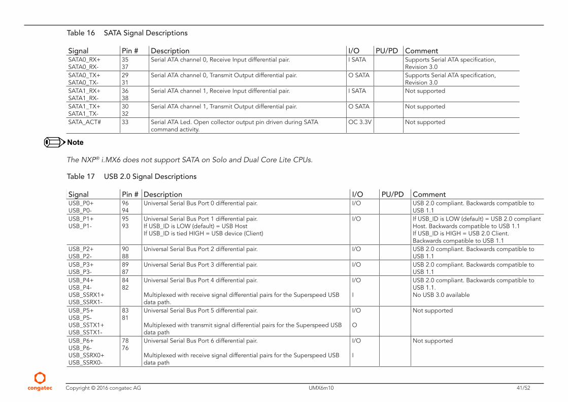
5.4 SATA
The NXP® i.MX6 Cortex A9 processor on the conga-UMX6 supports one SATA port only. The conga-UMX6 offers this SATA port on the MXM connector. The port supports SATA I (1.5Gbps) and SATA II (3Gbps) and is compliant with SATA specification 3.0, AHCI specification 1.3 and Advanced Microcontroller Bus Architecture (AMBA) specification 2.0.
Note
Solo Core and Dual Lite variants do not support SATA.
5.5 USB 2.0
The conga-UMX6 offers four USB 2.0 host ports and one USB 2.0 OTG port. For more information, see section 8.5 “USB Port Connections”.
Copyright © 2016 congatec AG UMX6m10 24/52
5.6 SD/SDIO/MMC
The conga-UMX6 offers an SDIO interface on the MXM connector via the NXP® i.MX6 SD4 port. The interface supports SDIO Revision 1.1, SD Memory Card Specification Revision 3.0 and MMC Revision 4.4.
5.7 HDA/I2S/AC’97
The conga-UMX6 uses the I2S format for audio signals. These signals are derived from the Synchronous Serial Interface (SSI) of the NXP® i.MX6 processor.
The SSI is a full duplex serial port that allows communication with external devices using a variety of serial protocols. The I2S protocol is part of the protocols supported by the NXP® i.MX6 Cortex A9 processor. The SSI supports up to 1.4 Mbps.
Note
The conga-UMX6 currently supports only I2S format.
5.8 LVDS
The conga-UMX6 offers 18bit or 24 bit dual LVDS channel, with up to 170 Mhz pixel clock. Each channel consists of one clock pair and four data pairs. The LVDS interface supports up to 85 MHz per interface (e.g 1366x768 @ 60 Hz + 35 % blanking) for single channel output and up to 170 MHz pixel clock (e.g 1600x1200 @ 60Hz + 35 % blanking) for dual channel output.
The LVDS ports can be configured as:
• One single channel output
• One dual channel output: single input split to two output channels
• Two identical outputs: single input sent to both output channels
• Two independent outputs: two inputs sent, each to a different output channel
Note
The LVDS interface can be configured as a single channel, a dual channel or as two independent single LVDS channels. The actual configuration depends on the Operating System. For more information, contact congatec technical solution center.
Three independent displays are possible when connected as two single LVDS channel and one HDMI interface.
Copyright © 2016 congatec AG UMX6m10 25/52
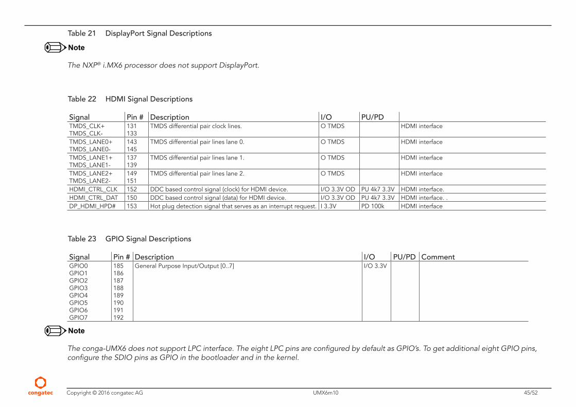
5.9 HDMI
The conga-UMX6 offers an HDMI interface on the MXM connector. The interface supports hot plug detection.
5.10 GPIO
The conga-UMX6 supports eight GPIO pins. These pins are shared with the LPC interface according to the Qseven Specification 2.0. The General Purpose Input/Output pins can be configured as inputs or outputs. When configured as output, it is possible to write to an internal register to control the state driven on the output pin. When configured as input, the input state can be detected by reading the status of an internal register. To select the GPIO mode, configure the IOMUX.
Note
The conga-UMX6 does not support the Low Pin Count (LPC) signals.
5.11 SPI
The NXP® i.MX6 processor provides Enhanced Configurable Serial Peripheral Interfaces (ECSPIs) capable of up to 66 Mbps write speed and 31 Mbps read speed. The ECSPI interfaces offer full-duplex, synchronous serial interface with maximum operation frequency up to the reference clock frequency. It can be configured to support Master/Slave modes and four chip selects to support multiple peripherals.
The conga-UMX6 offers one SPI interface on the edge finger connector. Another SPI interface from the NXP® i.MX6 processor is connected to the 32 Mbit SPI Flash memory onboard the conga-UMX6. The conga-UMX6 is programmed to boot from the bootloader contained in the SPI flash memory.
5.12 CAN Bus
The conga-UMX6 supports CAN bus. The CAN controller performs communication in accordance with the CAN Protocol Version 2.0B Active1 (standard format and extended format). The bit rate can be programmed to a maximum of 1 Mbit/s, depending on the technology used. To connect the CAN controller module to the CAN bus, add transceiver hardware.
A complete description of the CAN controller registers and functionality is beyond the scope of this user’s guide. Consult NXP’s i.MX6 processor reference manual for additional information about this interface.
Copyright © 2016 congatec AG UMX6m10 26/52
5.13 Manufacturing/JTAG Interface
The manufacturing signals defined in Qseven Specification 2.0 are reserved for manufacturing or debugging purposes. The conga-UMX6 offers this interface as a 10-pin JTAG interface, for debugging purposes. This interface is connected to the JTAG controller of the NXP® i.MX6 processor. The JTAG control fuses permits or restricts JTAG access to secured resources.
Note
For compatible JTAG adapters, contact the congatec support team or order the Nit6X_JTAG from Boundary Devices.
Note
The conga-UMX6 offers an additional UART interface. This interface is multiplexed with the JTAG interface on the MFG port. The MFG port supports only JTAG by default (MFG_NC4 pin is set to active high).
To support the second UART on the MFG port, set MFG_NC4 pin to active low.
5.14 Power Control
PWGIN
The PWGIN (pin 26) can be connected to an external power good circuit or may be used as a manual reset input. To use PWGIN as a manual reset input, ground the pin via a momentary-contact, push-button switch. When external circuitry asserts this signal, you need an open-drain driver to hold the signal for 15ms or more, to initiate a reset. Using this input is optional.
For more information, see the note below.
SUS_S3#
The SUS_S3# (pin 18) signal shuts off power to all runtime system components that are not maintained during suspend mode. This output signal is connected to the Power Management Integrated Circuit (PMIC) and driven by software via GPIO. See table 21 “Power Management Signal Descriptions” for more information.
PWRBTN#
When using ATX-style power supplies, PWRBTN# (pin 20) is used to connect to a momentary-contact, active-low debounced push-button input while the other terminal on the push-button must be connected to ground. This signal is internally pulled up to 3V_SB with a 10k resistor. When PWRBTN# is asserted it indicates that an operator wants to turn the power on or off.

Copyright © 2016 congatec AG UMX6m10 27/52
Note
The conga-UMX6 starts immediately power is applied to the module’s +5v input rail. To shut down the module, use the linux command “poweroff”. You can also shut down the module by pressing the power button; however, this depends on the installed operating system. If the system is shut down or in standby, pressing the power button restores the system back to full-on state. When the SoC’s main power supply is off and you press the power button for more than 750 ms, the power IC will turn the SoC power on.
If you want the system to remain turned off even when the +5V input power rail is active (ATX-style), use an external logic to prevent the system from bo the power IC will turn the SoC power on oting via power good signal (PWGIN). The external logic should release the PWGIN signal when the desired event occurs (e.g pressing the power button).
Power Supply Implementation Guidelines
5 volt input power is the sole operational power source for the conga-UMX6. The remaining necessary voltages are internally generated on the module using onboard voltage regulators. When designing a power supply for a conga-UMX6 application, a carrier board designer should be aware of the important information below:
• It has been noticed that on some occasions, problems occur when using a 5V power supply that produces non monotonic voltage when powered up. The problem is that some internal circuits on the module (e.g. clock-generator chips) will generate their own reset signals when the supply voltage exceeds a certain voltage threshold. A voltage dip after passing this threshold may lead to these circuits becoming confused resulting in a malfunction. It must be mentioned that this problem is quite rare but has been observed in some mobile power supply applications. The best way to ensure that this problem is not encountered is to observe the power supply rise waveform through the use of an oscilloscope to determine if the rise is indeed monotonic and does not have any dips. This should be done during the power supply qualification phase therefore ensuring that the above mentioned problem doesn’t arise in the application. For more information about this issue visit www.formfactors.org and view page 25 figure 7 of the document “ATX12V Power Supply Design Guide V2.2”.
Inrush and Maximum Current Peaks on VCC_5V_SB and VCC
The inrush-current on the conga-UMX6 VCC_5V_SB power rail can go up as high as 2.3A for a maximum of 100µS. Sufficient decoupling capacitance must be implemented to ensure proper power-up sequencing.
The maximum peak-current on the conga-UMX6 VCC (5V) power rail can be as high as 3.0A. This requires that the power supply be properly dimensioned.
Note
For more information about power control event signals refer to the Qseven® specification.
Copyright © 2016 congatec AG UMX6m10 28/52
5.15 Power Management
The conga-UMX6 has a 14 channel configurable Power Management Integrated Circuit (PMIC) onboard. The PMIC provides a cost effective programmable power management solution for a wide range of applications. This high efficiency, configurable power management IC is designed to work seamlessly with NXP® processors. The NXP® i.MX6 cortex A9 processor uses advanced integration Power Management Unit (PMU) to reduce supply connections. The PMIC complements the processor’s internal regulators in providing a complete and simple way to supply voltage domain with different voltages when needed.
The PMIC features four bulk regulators (up to six independent outputs), one boost regulator, six general purpose LDOs, one switch/LDO combination and a DDR voltage reference to supply voltages for the application processor and peripheral devices. With integrated memory power, RTC supply and additional bulk and linear regulators to power system peripherals, multiple point of power supply across the PCB is drastically reduced.
5.16 Watchdog
The watchdog timer (WDOG) protects against system failures by providing a method of escaping from unexpected events or programming errors. The software must periodically service the watchdog timer once the WDOG is activated. Without the servicing, the timer times out.
The NXP® i.MX6 processor on the conga-UMX6 offers two watchdog timers - a watchdog timer integrated within the ARM Cortex A9 platform and a TrustZone watchdog timer.
5.17 I2C Bus
The conga-UMX6 offers three I2C interfaces - I2CI, I2C2 & I2C3 on the Qseven edge connector. The I2C2 and I2C3 buses on the connector are shared with some onboard devices (I2C3 is shared with LVDS and RTC whereas the I2C2 is shared with HDMI). The I2C1 is routed directly to the edge connector, without sharing.
The I2C interfaces support up to 400 kbps, depending on the pin loading and timing characteristics.
Note
We implemented a multiplexer on the I2C2 interface. The multiplexer separates the PMIC functions from other devices (e.g HDMI) that share the bus. Therefore, for I2C bus to function properly, use the latest kernel from the git.congatec.com/public server or at least ensure that the congatec I2C multiplexer patches are applied to the desired kernel.
On revision X.2, the I2C3 is connected to the SBM bus pins by default.
Copyright © 2016 congatec AG UMX6m10 29/52
6 Additional Features
6.1 High Assurance Boot (HAB)
The High Assurance Boot is a software library executed in internal ROM on the NXP® processor at boot time, which among other things, authenticates software in external memory by verifying digital signatures. The HAB enables the ROM to authenticate software which executes immediately after ROM, by using digital signatures. This software is usually a bootloader. The High Assurance Boot component of the ROM protects against the potential threat of attackers modifying areas of code or data in programmable memory to make it behave in an incorrect manner.
6.2 Dedicated Hardware Accelerators
The NXP® i.MX6 processor uses dedicated hardware accelerators to meet the targeted multimedia performance. The use of hardware accelerators is a key factor in obtaining high performance at low power consumption while having the CPU core relatively free for performing other tasks. The hardware accelerators available in the processor are VPU, IPUv3H, 3D GPU, 2D GPU, OpenVG 1.1 GPU and Asynchronous Sample Rate Converter (ASRC).
6.3 Power Management
The NXP® i.MX6 processor integrates power management functions to simplify system power management requirements. The processor provides power management units for offering power to various Soc domains. Temperature sensor for monitoring the die temperature is also provided.
Dynamic Voltage and Frequency Scaling techniques, software state retention, power gating and various levels of system power mode are supported. The use of simple and low-cost power regulators in place of complicated external power management ICs reduces system design cost.
6.4 Dynamic Voltage and Frequency Scaling
Dynamic Voltage and Frequency Scaling is a power management technique used in changing the clock frequency and/or the operating voltage of a processor based on system performance requirements at any point in time. This scaling is normally carried out during less demanding periods of nominal run speed. In General, it helps in balancing the performance demands of processor with the high amount of power needed to satisfy those demands.
Copyright © 2016 congatec AG UMX6m10 30/52
6.5 Smart Speed Technology
The NXP’s Smart Speed Technology with enhanced Cycles Per Instruction (eCPI) determines the speed of the processor by the set of tasks to be performed instead of the clock speed. The set of tasks determines the execution units needed to make sure the system work more efficiently. This ensures that the system provides enough performance without wasting resources.
With the Smart Speed Technology, several execution units work in parallel, thereby providing higher processor speed at lower power consumption. System parallelism is accomplished via the Smart Speed crossbar switch that nearly eliminates wait states. This results in improved processor performance without power consumption penalty associated with higher operating frequencies.
By employing Smart Speed Technology, portable devices can run longer, retain smaller form factors and support more innovative applications without substantially increasing the battery power.
6.6 Suspend Mode
The Suspend Mode feature is available on the conga-UMX6.

Copyright © 2016 congatec AG UMX6m10 31/52
7 conga Tech NotesThe conga-UMX6 has some technological features that require additional explanation. The following section will give the reader a better understanding of some of these features.
7.1 ARM Technologies
7.1.1 Media Processing Engine (MPE-NEON)
The Media Processing Engine (MPE-NEON) is a single instruction multiple data (SIMD) instruction set that provides flexible and powerful acceleration for media and signal processing applications. Support for a wide range of multimedia codecs with fewer cycles helps in enhancing user experience. NEON is used for multimedia data processing.
7.1.2 Jazelle DBX
The Jazelle is an instruction set that introduces technological infrastructure for running java codes faster than the software based java virtual machine. The Jazelle DBX (Direct Bytecode eXecution) enabled cores execute the majority of Java bytecodes in hardware. No modification is required in the application code to take advantage of this technology. To configure and turn on the Jazelle DBX, the software support code needs to be integrated into a Java Virtual Machine (JVM). Contact ARM for further information on how to obtain the software support code.
7.1.3 TrustZone
The ARM TrustZone technology is a security extension that provides additional dedicated security to a System on Chip (SoC). This technology aims to provide a framework that enables a device to counter many of the specific threats that it will experience. The security of the system is achieved by partitioning all of the SoC’s hardware and software resources so that they exist in one of two worlds - the secure world (more trusted) and the normal world (less trusted). The memory and peripherals are then made aware of the operating world of the core and may use
this to provide access control to secrets and code in the device.
7.1.4 Floating Point Unit
The Floating Point Unit (FPU) provides significant acceleration for both single and double precision scalar Floating-Point operations. It provides industry leading image processing, graphics and scientific computation capabilities. The FPU provides an optimized solution in performance, power and area for embedded applications and high performance for general purpose applications.

Copyright © 2016 congatec AG UMX6m10 32/52
7.2 NXP® i.MX6 Processor Features
7.2.1 Temperature Monitor (TEMPMON)
The NXP® i.MX6 Cortex A9 processors have a temperature sensor module that implements a temperature sensor/conversion function based on a temperature-dependent voltage to time conversion.
The module features an alarm function that can raise an interrupt signal if the temperature is above a specified threshold. A self repeating mode can also be programmed which executes a temperature sensing operation based on a programmed delay.
Software can use this module to monitor the on-die temperature and take appropriate actions such as throttling back the core frequency when a temperature interrupt is set.
During normal system operation, software can use the temperature sensor counter output in conjunction with the fused temperature calibration data to determine the on-die operational temperature or to set an over-temperature interrupt alarm to within a couple of degree centigrade.
7.3 Thermal Management
To meet low power design requirement while maintaining a high performance operation, the NXP® iMX6 incorporated several low power design techniques. Even with these techniques, it is vital to manage the heat dissipation of the module in accordance with internal and external conditions.
The conga-UMX6 employs basically two types of thermal management strategies:
Active Cooling
During this cooling policy, the operating system turns the fan on/off. Though the active thermal management technique provides better heat dissipation and lower thermal resistances, the cooling solutions are however expensive and have large form factors.
Passive Cooling
The passive cooling policy employs the technique of enhancing conduction and natural convection. This passive thermal management procedure provides cost effective cooling solutions up to certain power levels without introducing reliability concerns. Some of these techniques typically used are thermal gap fillers, heatspreaders and heat shields.
Copyright © 2016 congatec AG UMX6m10 33/52
7.4 Audio Mux
Audio Mux (AUDMUX) is one of the modules found in the audio subsystem of the NXP® i.MX6 processor. It provides flexible programmable routing of the on-chip serial interfaces to and from off-chip devices. The AUDMUX includes internal port that connect to the processor serial interfaces and external ports that connect to off-chip audio devices. Connection is established by configuring the appropriate host and peripheral ports. Though controlled by ARM, the AUDMUX can route data even when the ARM is in a low-power mode.
7.5 LVDS Bridge
The LVDS Bridge (LDB) supports the flow of synchronous RGB data from the Image Processing Unit to external devices through LVDS interface. This support includes synchronization and control capabilities, connectivitity to relevant devices as well as proper data arrangement as required by the external display receiver and by LVDS display standards.
7.6 USB Port Connections
The conga-UMX6 offers a total of 5 USB ports (one USB OTG port and four host ports). The four host-only ports are implemented by routing one host-only port (USB H1) from the NXP® i.MX6 processor to the conga-UMX6 edge finger via a SMSC USB Hub.
The USB_OTG port (OTG client) of the conga-UMX6 is routed directly to the USB_OTG port of the i.MX6 processor. This port can drop the hosting role and act as a normal USB device when conga-UMX6 is attached to another host. The client/host role is controlled via USB_ID signal. If the USB_ID signal is asserted high, the OTG port is set to client and if asserted low, the OTG port is set to host.
For more information refer to the USB routing diagram shown below:

Copyright © 2016 congatec AG UMX6m10 34/52
conga-UMX6 USB Routing Diagram
Freescale® i.MX6ARM Cortex A9
Processor
SMSCUSBHUB
USB 0 (Host only)
USB 2 (Host only)
USB 3 (Host only)
USB 4 (Host only)
USB 1 (Host/Client)
USB Device
USB Host1
USB OTG
Copyright © 2016 congatec AG UMX6m10 35/52
8 Interface - Signal Descriptions and Pinout TablesThe following section describes the signals found on Qseven® module’s edge fingers and the interfaces implemented on the conga-UMX6. The table below describes the terminology used in this section for the Signal Description tables. The PU/PD column indicates if a Qseven® module pull-up or pull-down resistor has been used, if the field entry area in this column for the signal is empty, then no pull-up or pull-down resistor has been implemented by congatec. The “#” symbol at the end of the signal name indicates that the active or asserted state occurs when the signal is at a low voltage level. When “#” is not present, the signal is asserted when at a high voltage level.
Note
The signal description tables do not list internal pull-ups or pull-downs implemented by the chip vendors, only pull-ups or pull-downs implemented by congatec are listed. For information about the internal pull-ups or pull-downs implemented by the chip vendors, refer to the respective chip’s datasheet.
Not all the signals described in this section are available on all conga-UMX6 variants. Use the article number of the module and refer to the options table on page 8 to determine the options available on the module.
Table 11 Signal Tables Terminology Descriptions
Term DescriptionI Input pinO Output pinOC Open collectorOD Open drainPP Push pullI/O Bi-directional Input/Output Pin3.3VSB 3.3V tolerant active in standby stateP Power inputNA Not applicableNC Not connectedPCIE PCI Express differential pair signals. In compliance with the PCI Express Base Specification 1.0a.GB_LAN Gigabit Ethernet Media Dependent Interface differential pair signals. In compliance with IEEE 802.3ab 1000Base-T Gigabit Ethernet Specification.USB Universal Serial Bus differential pair signals. In compliance with the Universal Serial Bus Specification 2.0SATA Serial Advanced Technology Attachment differential pair signals. In compliance with the Serial ATA High Speed Serialized AT Attachment Specification 1.0a.SPI Serial Peripheral Interface bus is a synchronous serial data link that operates in full duplex mode.CAN Controller Area Network bus is a vehicle bus standard that allows microcontrollers and devices to communicate with each other within a vehicle without a
host computer.LVDS Low-Voltage Differential Signaling differential pair signals. In compliance with the LVDS Owner's Manual 4.0.TMDS Transition Minimized Differential Signaling differential pair signals. In compliance with the Digital Visual Interface (DVI) Specification 1.0.CMOS Logic input or output.

Copyright © 2016 congatec AG UMX6m10 36/52
Table 12 Edge Finger Pinout
Pin Signal Pin Signal1 GND 2 GND 3 GBE_MDI3- 4 GBE_MDI2- 5 GBE_MDI3+ 6 GBE_MDI2+7 GBE_LINK100# 8 GBE_LINK1000#9 GBE_MDI1- 10 GBE_MDI0-11 GBE_MDI1+ 12 GBE_MDI0+13 GBE_LINK# 14 GBE_ACT# 15 GBE_CTREF (*) 16 SUS_S5# 17 WAKE# 18 SUS_S3# 19 SUS_STAT# 20 PWRBTN# 21 SLP_BTN# 22 LID_BTN# 23 GND 24 GND 25 GND 26 PWGIN 27 BATLOW# 28 RSTBTN# 29 SATA0_TX+ 30 SATA1_TX+(*)31 SATA0_TX- 32 SATA1_TX- (*)33 SATA_ACT# 34 GND35 SATA0_RX+ 36 SATA1_RX+ (*)37 SATA0_RX- 38 SATA1_RX- (*)39 GND 40 GND41 BIOS_DISABLE# / BOOT_ALT# 42 SDIO_CLK43 SDIO_CD# 44 SDIO_LED45 SDIO_CMD 46 SDIO_WP47 SDIO_PWR# 48 SDIO_DAT149 SDIO_DAT0 50 SDIO_DAT351 SDIO_DAT2 52 SDIO_DAT553 SDIO_DAT4 54 SDIO_DAT755 SDIO_DAT6 56 USB_DRIVE_VBUS57 GND 58 GND59 HDA_SYNC / I2S_WS 60 GP1_I2C_CLK61 HDA_RST# / I2S_RST# 62 GP1_I2C_DAT63 HDA_BITCLK / I2S_CLK 64 SMB_ALERT# 65 HDA_SDI / I2S_SDI 66 GP0_I2C_CLK67 HDA_SDO / I2S_SDO 68 GP0_I2C_DAT69 THRM# 70 WDTRIG# 71 THRMTRIP# 72 WDOUT 73 GND 74 GND 75 USB_P7- / USB_SSTX0- (*) 76 USB_P6- / USB_SSRX0- (*)
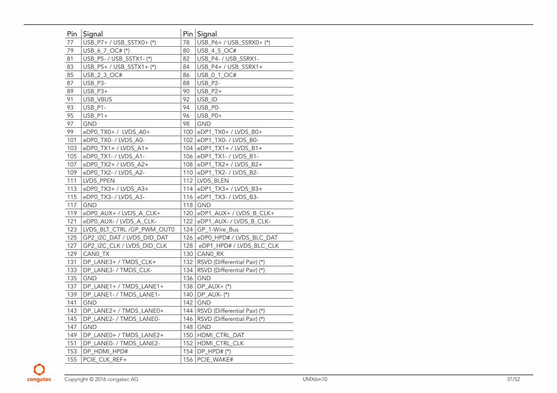
Copyright © 2016 congatec AG UMX6m10 37/52
Pin Signal Pin Signal77 USB_P7+ / USB_SSTX0+ (*) 78 USB_P6+ / USB_SSRX0+ (*)79 USB_6_7_OC# (*) 80 USB_4_5_OC#81 USB_P5- / USB_SSTX1- (*) 82 USB_P4- / USB_SSRX1-83 USB_P5+ / USB_SSTX1+ (*) 84 USB_P4+ / USB_SSRX1+85 USB_2_3_OC# 86 USB_0_1_OC#87 USB_P3- 88 USB_P2-89 USB_P3+ 90 USB_P2+91 USB_VBUS 92 USB_ID 93 USB_P1- 94 USB_P0-95 USB_P1+ 96 USB_P0+97 GND 98 GND99 eDP0_TX0+ / LVDS_A0+ 100 eDP1_TX0+ / LVDS_B0+ 101 eDP0_TX0- / LVDS_A0- 102 eDP1_TX0- / LVDS_B0-103 eDP0_TX1+ / LVDS_A1+ 104 eDP1_TX1+ / LVDS_B1+ 105 eDP0_TX1- / LVDS_A1- 106 eDP1_TX1- / LVDS_B1-107 eDP0_TX2+ / LVDS_A2+ 108 eDP1_TX2+ / LVDS_B2+109 eDP0_TX2- / LVDS_A2- 110 eDP1_TX2- / LVDS_B2-111 LVDS_PPEN 112 LVDS_BLEN 113 eDP0_TX3+ / LVDS_A3+ 114 eDP1_TX3+ / LVDS_B3+115 eDP0_TX3- / LVDS_A3- 116 eDP1_TX3- / LVDS_B3-117 GND 118 GND 119 eDP0_AUX+ / LVDS_A_CLK+ 120 eDP1_AUX+ / LVDS_B_CLK+121 eDP0_AUX- / LVDS_A_CLK- 122 eDP1_AUX- / LVDS_B_CLK-123 LVDS_BLT_CTRL /GP_PWM_OUT0 124 GP_1-Wire_Bus125 GP2_I2C_DAT / LVDS_DID_DAT 126 eDP0_HPD# / LVDS_BLC_DAT127 GP2_I2C_CLK / LVDS_DID_CLK 128 eDP1_HPD# / LVDS_BLC_CLK129 CAN0_TX 130 CAN0_RX 131 DP_LANE3+ / TMDS_CLK+ 132 RSVD (Differential Pair) (*)133 DP_LANE3- / TMDS_CLK- 134 RSVD (Differential Pair) (*)135 GND 136 GND 137 DP_LANE1+ / TMDS_LANE1+ 138 DP_AUX+ (*)139 DP_LANE1- / TMDS_LANE1- 140 DP_AUX- (*)141 GND 142 GND 143 DP_LANE2+ / TMDS_LANE0+ 144 RSVD (Differential Pair) (*)145 DP_LANE2- / TMDS_LANE0- 146 RSVD (Differential Pair) (*)147 GND 148 GND 149 DP_LANE0+ / TMDS_LANE2+ 150 HDMI_CTRL_DAT151 DP_LANE0- / TMDS_LANE2- 152 HDMI_CTRL_CLK153 DP_HDMI_HPD# 154 DP_HPD# (*)155 PCIE_CLK_REF+ 156 PCIE_WAKE#

Copyright © 2016 congatec AG UMX6m10 38/52
Pin Signal Pin Signal157 PCIE_CLK_REF- 158 PCIE_RST# 159 GND 160 GND 161 PCIE3_TX+ (*) 162 PCIE3_RX+ (*)163 PCIE3_TX- (*) 164 PCIE3_RX- (*)165 GND 166 GND 167 PCIE2_TX+ (*) 168 PCIE2_RX+ (*)169 PCIE2_TX- (*) 170 PCIE2_RX- (*)171 UART0_TX 172 UART0_RTS#173 PCIE1_TX+ (*) 174 PCIE1_RX+ (*)175 PCIE1_TX- (*) 176 PCIE1_RX- (*)177 UART0_RX 178 UART0_CTS#179 PCIE0_TX+ 180 PCIE0_RX+ 181 PCIE0_TX- 182 PCIE0_RX- 183 GND 184 GND 185 LPC_AD0 / GPIO0 186 LPC_AD1 / GPIO1187 LPC_AD2 / GPIO2 188 LPC_AD3 / GPIO3189 LPC_CLK / GPIO4 190 LPC_FRAME# / GPIO5191 SERIRQ / GPIO6 192 LPC_LDRQ# / GPIO7193 VCC_RTC 194 SPKR / GP_PWM_OUT2195 FAN_TACHOIN / GP_TIMER_IN 196 FAN_PWMOUT / GP_PWM_OUT1197 GND 198 GND 199 SPI_MOSI 200 SPI_CS0# 201 SPI_MISO 202 SPI_CS1# 203 SPI_SCK 204 MFG_NC4205 VCC_5V_SB 206 VCC_5V_SB 207 MFG_NC0 208 MFG_NC2 209 MFG_NC1 210 MFG_NC3 211 VCC 212 VCC213 VCC 214 VCC215 VCC 216 VCC217 VCC 218 VCC219 VCC 220 VCC221 VCC 222 VCC223 VCC 224 VCC225 VCC 226 VCC227 VCC 228 VCC229 VCC 230 VCC
Note
The conga-UMX6 does not support the signals marked with asterisk symbol (*).
Copyright © 2016 congatec AG UMX6m10 39/52
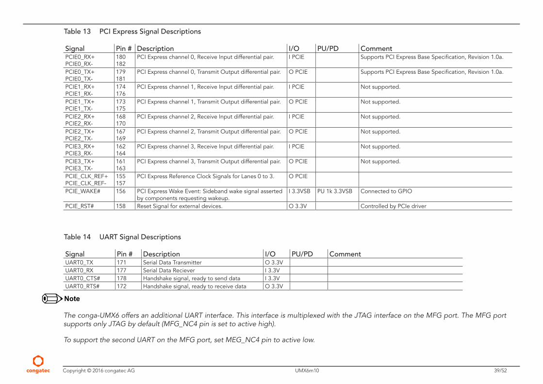
Table 13 PCI Express Signal Descriptions
Signal Pin # Description I/O PU/PD CommentPCIE0_RX+PCIE0_RX-
180182
PCI Express channel 0, Receive Input differential pair. I PCIE Supports PCI Express Base Specification, Revision 1.0a.
PCIE0_TX+PCIE0_TX-
179181
PCI Express channel 0, Transmit Output differential pair. O PCIE Supports PCI Express Base Specification, Revision 1.0a.
PCIE1_RX+PCIE1_RX-
174176
PCI Express channel 1, Receive Input differential pair. I PCIE Not supported.
PCIE1_TX+PCIE1_TX-
173175
PCI Express channel 1, Transmit Output differential pair. O PCIE Not supported.
PCIE2_RX+PCIE2_RX-
168170
PCI Express channel 2, Receive Input differential pair. I PCIE Not supported.
PCIE2_TX+PCIE2_TX-
167169
PCI Express channel 2, Transmit Output differential pair. O PCIE Not supported.
PCIE3_RX+PCIE3_RX-
162164
PCI Express channel 3, Receive Input differential pair. I PCIE Not supported.
PCIE3_TX+PCIE3_TX-
161163
PCI Express channel 3, Transmit Output differential pair. O PCIE Not supported.
PCIE_CLK_REF+PCIE_CLK_REF-
155157
PCI Express Reference Clock Signals for Lanes 0 to 3. O PCIE
PCIE_WAKE# 156 PCI Express Wake Event: Sideband wake signal asserted by components requesting wakeup.
I 3.3VSB PU 1k 3.3VSB Connected to GPIO
PCIE_RST# 158 Reset Signal for external devices. O 3.3V Controlled by PCIe driver
Table 14 UART Signal Descriptions
Signal Pin # Description I/O PU/PD CommentUART0_TX 171 Serial Data Transmitter O 3.3VUART0_RX 177 Serial Data Reciever I 3.3VUART0_CTS# 178 Handshake signal, ready to send data I 3.3VUART0_RTS# 172 Handshake signal, ready to receive data O 3.3V
Note
The conga-UMX6 offers an additional UART interface. This interface is multiplexed with the JTAG interface on the MFG port. The MFG port supports only JTAG by default (MFG_NC4 pin is set to active high).
To support the second UART on the MFG port, set MEG_NC4 pin to active low.

Copyright © 2016 congatec AG UMX6m10 40/52
Table 15 Ethernet Signal Descriptions
Signal Pin # Description I/O PU/PD CommentGBE_MDI0+GBE_MDI0-
1210
Media Dependent Interface (MDI) differential pair 0. The MDI can operate in 1000, 100, and 10Mbit/sec modes.This signal pair is used for all modes.
I/O Analog Twisted pair signals for external transformer.
GBE_MDI1+GBE_MDI1-
119
Media Dependent Interface (MDI) differential pair 1. The MDI can operate in 1000, 100, and 10Mbit/sec modes.This signal pair is used for all modes.
I/O Analog Twisted pair signals for external transformer.
GBE_MDI2+GBE_MDI2-
64
Media Dependent Interface (MDI) differential pair 2. The MDI can operate in 1000, 100, and 10Mbit/sec modes.This signal pair is only used for 1000Mbit/sec Gigabit Ethernet mode.
I/O Analog Twisted pair signals for external transformer.
GBE_MDI3+GBE_MDI3-
53
Media Dependent Interface (MDI) differential pair 3. The MDI can operate in 1000, 100, and 10Mbit/sec modes.This signal pair is only used for 1000Mbit/sec Gigabit Ethernet mode.
I/O Analog Twisted pair signals for external transformer.
GBE_CTREF 15 Reference voltage for carrier board Ethernet channel 0 magnetics center tap. The reference voltage is determined by the requirements of the module's PHY and may be as low as 0V and as high as 3.3V.The reference voltage output should be current limited on the module. In a case in which the reference is shorted to ground, the current must be limited to 250mA or less.
REF Not Supported
GBE_LINK# 13 Ethernet controller 0 link indicator, active low. O 3.3V PP PD 1k GBE0_LINK# is a bootstrap signal (see note below)GBE_LINK100# 7 Ethernet controller 0 100Mbit/sec link indicator, active low. O 3.3V PP PU 4k99
2,5VSBNot Supported. Internally connected to GBE_ACT#.GBE0_LINK100# is a bootstrap signal (see note below)
GBE_LINK1000# 8 Ethernet controller 0 1000Mbit/sec link indicator, active low. O 3.3V PP PD 1k Not Supported. Internally connected to GBE_LINK#.GBE0_LINK1000# is a bootstrap signal (see note below)
GBE_ACT# 14 Ethernet controller 0 activity indicator, active low. O 3.3V PP PU 4k99 2,5VSB
GBE0_ACT# is a bootstrap signal (see note below)
Note
The theoretical maximum performance of the Gigabit Ethernet interface is limited to 470 Mbps (total for Tx and Rx) due to internal bus throughput limitations. The actual measured performance in optimized environment is up to 400 Mbps. For more information, consult NXP’s Errata ERR004512.
Some signals have special functionality during the reset process. They may bootstrap some basic important functions of the module. For more information, refer to section 9.1 of this user’s guide.
Copyright © 2016 congatec AG UMX6m10 41/52
Table 16 SATA Signal Descriptions
Signal Pin # Description I/O PU/PD CommentSATA0_RX+SATA0_RX-
3537
Serial ATA channel 0, Receive Input differential pair. I SATA Supports Serial ATA specification, Revision 3.0
SATA0_TX+SATA0_TX-
2931
Serial ATA channel 0, Transmit Output differential pair. O SATA Supports Serial ATA specification, Revision 3.0
SATA1_RX+SATA1_RX-
3638
Serial ATA channel 1, Receive Input differential pair. I SATA Not supported
SATA1_TX+SATA1_TX-
3032
Serial ATA channel 1, Transmit Output differential pair. O SATA Not supported
SATA_ACT# 33 Serial ATA Led. Open collector output pin driven during SATA command activity.
OC 3.3V Not supported
Note
The NXP® i.MX6 does not support SATA on Solo and Dual Core Lite CPUs.
Table 17 USB 2.0 Signal Descriptions
Signal Pin # Description I/O PU/PD CommentUSB_P0+USB_P0-
9694
Universal Serial Bus Port 0 differential pair. I/O USB 2.0 compliant. Backwards compatible to USB 1.1
USB_P1+USB_P1-
9593
Universal Serial Bus Port 1 differential pair.If USB_ID is LOW (default) = USB HostIf USB_ID is tied HIGH = USB device (Client)
I/O If USB_ID is LOW (default) = USB 2.0 compliant Host. Backwards compatible to USB 1.1If USB_ID is HIGH = USB 2.0 Client. Backwards compatible to USB 1.1
USB_P2+USB_P2-
9088
Universal Serial Bus Port 2 differential pair. I/O USB 2.0 compliant. Backwards compatible to USB 1.1
USB_P3+USB_P3-
8987
Universal Serial Bus Port 3 differential pair. I/O USB 2.0 compliant. Backwards compatible to USB 1.1
USB_P4+USB_P4-USB_SSRX1+USB_SSRX1-
8482
Universal Serial Bus Port 4 differential pair.
Multiplexed with receive signal differential pairs for the Superspeed USB data path.
I/O
I
USB 2.0 compliant. Backwards compatible to USB 1.1.No USB 3.0 available
USB_P5+USB_P5-USB_SSTX1+USB_SSTX1-
8381
Universal Serial Bus Port 5 differential pair.
Multiplexed with transmit signal differential pairs for the Superspeed USB data path
I/O
O
Not supported
USB_P6+USB_P6-USB_SSRX0+USB_SSRX0-
7876
Universal Serial Bus Port 6 differential pair.
Multiplexed with receive signal differential pairs for the Superspeed USB data path
I/O
I
Not supported
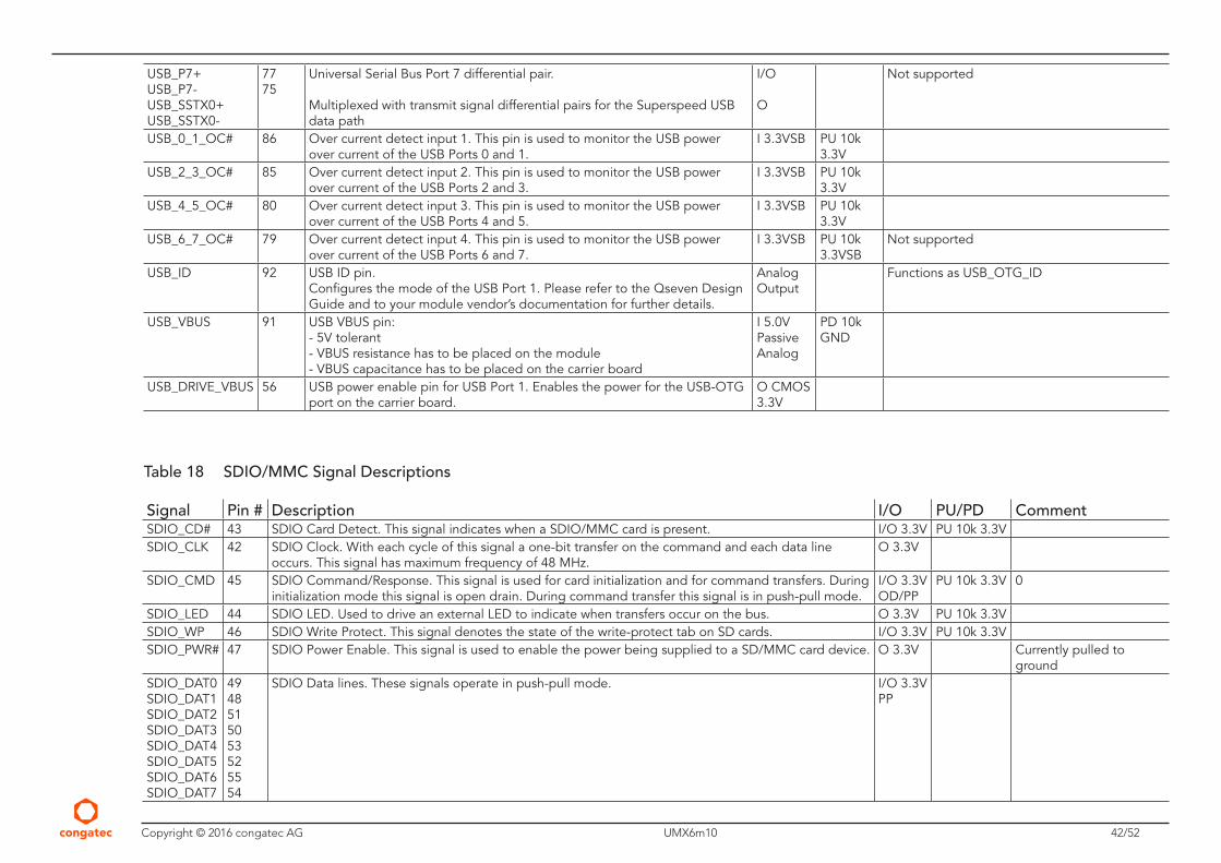
Copyright © 2016 congatec AG UMX6m10 42/52
USB_P7+USB_P7-USB_SSTX0+USB_SSTX0-
7775
Universal Serial Bus Port 7 differential pair.
Multiplexed with transmit signal differential pairs for the Superspeed USB data path
I/O
O
Not supported
USB_0_1_OC# 86 Over current detect input 1. This pin is used to monitor the USB power over current of the USB Ports 0 and 1.
I 3.3VSB PU 10k 3.3V
USB_2_3_OC# 85 Over current detect input 2. This pin is used to monitor the USB power over current of the USB Ports 2 and 3.
I 3.3VSB PU 10k 3.3V
USB_4_5_OC# 80 Over current detect input 3. This pin is used to monitor the USB power over current of the USB Ports 4 and 5.
I 3.3VSB PU 10k 3.3V
USB_6_7_OC# 79 Over current detect input 4. This pin is used to monitor the USB power over current of the USB Ports 6 and 7.
I 3.3VSB PU 10k 3.3VSB
Not supported
USB_ID 92 USB ID pin.Configures the mode of the USB Port 1. Please refer to the Qseven Design Guide and to your module vendor’s documentation for further details.
Analog Output
Functions as USB_OTG_ID
USB_VBUS 91 USB VBUS pin:- 5V tolerant- VBUS resistance has to be placed on the module- VBUS capacitance has to be placed on the carrier board
I 5.0VPassive Analog
PD 10k GND
USB_DRIVE_VBUS 56 USB power enable pin for USB Port 1. Enables the power for the USB-OTG port on the carrier board.
O CMOS 3.3V
Table 18 SDIO/MMC Signal Descriptions
Signal Pin # Description I/O PU/PD CommentSDIO_CD# 43 SDIO Card Detect. This signal indicates when a SDIO/MMC card is present. I/O 3.3V PU 10k 3.3VSDIO_CLK 42 SDIO Clock. With each cycle of this signal a one-bit transfer on the command and each data line
occurs. This signal has maximum frequency of 48 MHz.O 3.3V
SDIO_CMD 45 SDIO Command/Response. This signal is used for card initialization and for command transfers. During initialization mode this signal is open drain. During command transfer this signal is in push-pull mode.
I/O 3.3V OD/PP
PU 10k 3.3V 0
SDIO_LED 44 SDIO LED. Used to drive an external LED to indicate when transfers occur on the bus. O 3.3V PU 10k 3.3VSDIO_WP 46 SDIO Write Protect. This signal denotes the state of the write-protect tab on SD cards. I/O 3.3V PU 10k 3.3VSDIO_PWR# 47 SDIO Power Enable. This signal is used to enable the power being supplied to a SD/MMC card device. O 3.3V Currently pulled to
groundSDIO_DAT0SDIO_DAT1SDIO_DAT2SDIO_DAT3SDIO_DAT4SDIO_DAT5SDIO_DAT6SDIO_DAT7
4948515053525554
SDIO Data lines. These signals operate in push-pull mode. I/O 3.3V PP

Copyright © 2016 congatec AG UMX6m10 43/52
Table 19 HDA/I2S/SPDIF Signal Descriptions
Signal Pin # Description I/O PU/PD CommentHDA_RST#I2S_RST#
61 HD Audio/AC’97 Codec Reset.Multiplexed with I2S Codec Reset.
O 3.3V Connected to GPIO.
HDA_SYNCI2S_WS
59 Serial Bus Synchronization.Multiplexed with I2S Word Select from Codec.
O 3.3V
HDA_BITCLKI2S_CLK
63 HD Audio/AC’97 24 MHz Serial Bit Clock from Codec.Multiplexed with I2S Serial Data Clock from Codec.
O 3.3V
HDA_SDOI2S_SDO
67 HD Audio/AC’97 Serial Data Output to Codec.Multiplexed with I2S Serial Data Output from Codec.
O 3.3V
HDA_SDII2S_SDI
65 HD Audio/AC’97 Serial Data Input from Codec.Multiplexed with I2S Serial Data Input from Codec.
I 3.3V
Note
The conga-UMX6 currently supports only I2S format.
Table 20 LVDS Signal Descriptions
Signal Pin # Description I/O PU/PD CommentLVDS_PPEN 111 Controls panel power enable. O 3.3VLVDS_BLEN 112 Controls panel Backlight enable. O 3.3VLVDS_BLT_CTRL/GP_PWM_OUT0
123 Primary functionality is to control the panel backlight brightness via pulse width modulation (PWM). When not in use for this primary purpose it can be used as General Purpose PWM Output.
O 3.3V
LVDS_A0+LVDS_A0-eDP0_TX0+eDP0_TX0-
99101
LVDS primary channel differential pair 0.
Display Port primary channel differential pair 0.
O LVDS
LVDS_A1+LVDS_A1-eDP0_TX1+eDP0_TX1-
103105
LVDS primary channel differential pair 1.
Display Port primary channel differential pair 1.
O LVDS
LVDS_A2+LVDS_A2-eDP0_TX2+eDP0_TX2-
107109
LVDS primary channel differential pair 2.
Display Port primary channel differential pair 2.
O LVDS
LVDS_A3+LVDS_A3-eDP0_TX3+eDP0_TX3-
113115
LVDS primary channel differential pair 3.
Display Port primary channel differential pair 3.
O LVDS

Copyright © 2016 congatec AG UMX6m10 44/52
LVDS_A_CLK+LVDS_A_CLK-eDP0_AUX+eDP0_AUX-
119121
LVDS primary channel differential pair clock lines.
Display Port primary auxiliary channel.
O LVDS
LVDS_B0+LVDS_B0-eDP1_TX0+eDP1_TX0-
100102
LVDS secondary channel differential pair 0.
Display Port secondary channel differential pair 0.
O LVDS
LVDS_B1+LVDS_B1-eDP1_TX1+eDP1_TX1-
104106
LVDS secondary channel differential pair 1.
Display Port secondary channel differential pair 1.
O LVDS
LVDS_B2+LVDS_B2-eDP1_TX2+eDP1_TX2-
108110
LVDS secondary channel differential pair 2.
Display Port secondary channel differential pair 2.
O LVDS
LVDS_B3+LVDS_B3-eDP1_TX3+eDP1_TX3-
114116
LVDS secondary channel differential pair 3.
Display Port secondary channel differential pair 3.
O LVDS
LVDS_B_CLK+LVDS_B_CLK-eDP1_AUX+eDP1_AUX-
120122
LVDS secondary channel differential pair clock lines.
Display Port secondary auxiliary channel.
O LVDS
LVDS_DID_CLK /GP2_I2C_CLK
127 Primary functionality is DisplayID DDC clock line used for LVDS flat panel detection. If primary functionality is not used, it can be as General Purpose I²C bus clock line.
I/O 3.3VOD
PU 4k7 3.3V
LVDS_DID_DAT /GP2_I2C_DAT
125 Primary functionality DisplayID DDC data line used for LVDS flat panel detection. If primary functionality is not used it can be as General Purpose I²C bus data line.
I/O 3.3VOD
PU 4k7 3.3V
LVDS_BLC_CLK eDP1_HPD#
128 Control clock signal for external SSC clock chip. If the primary functionality is not used, it can be used as an emedded DisplayPort secondary Hotplug detection.
I/O 3.3VOD
PU 4k7 3.3V
Not supported
LVDS_BLC_DAT eDP0_HPD#
126 Control data signal for external SSC clock chip.If the primary functionality is not used, it can be used as an embedded DisplayPort primary Hotplug detection.
I/O 3.3VOD
PU 4k7 3.3V
Not supported
Note
The LVDS interface can be configured as a single channel, a dual channel or as two independent single LVDS channels. The actual configuration depends on the Operating System. For more information, contact congatec technical solution center.
Copyright © 2016 congatec AG UMX6m10 45/52
Table 21 DisplayPort Signal Descriptions
Note
The NXP® i.MX6 processor does not support DisplayPort.
Table 22 HDMI Signal Descriptions
Signal Pin # Description I/O PU/PD CommentTMDS_CLK+TMDS_CLK-
131133
TMDS differential pair clock lines. O TMDS HDMI interface
TMDS_LANE0+TMDS_LANE0-
143145
TMDS differential pair lines lane 0. O TMDS HDMI interface
TMDS_LANE1+TMDS_LANE1-
137139
TMDS differential pair lines lane 1. O TMDS HDMI interface
TMDS_LANE2+TMDS_LANE2-
149151
TMDS differential pair lines lane 2. O TMDS HDMI interface
HDMI_CTRL_CLK 152 DDC based control signal (clock) for HDMI device. I/O 3.3V OD PU 4k7 3.3V HDMI interface. HDMI_CTRL_DAT 150 DDC based control signal (data) for HDMI device. I/O 3.3V OD PU 4k7 3.3V HDMI interface. .DP_HDMI_HPD# 153 Hot plug detection signal that serves as an interrupt request. I 3.3V PD 100k HDMI interface
Table 23 GPIO Signal Descriptions
Signal Pin # Description I/O PU/PD CommentGPIO0GPIO1GPIO2GPIO3GPIO4GPIO5GPIO6 GPIO7
185186187188189190191192
General Purpose Input/Output [0..7] I/O 3.3V
Note
The conga-UMX6 does not support LPC interface. The eight LPC pins are configured by default as GPIO’s. To get additional eight GPIO pins, configure the SDIO pins as GPIO in the bootloader and in the kernel.
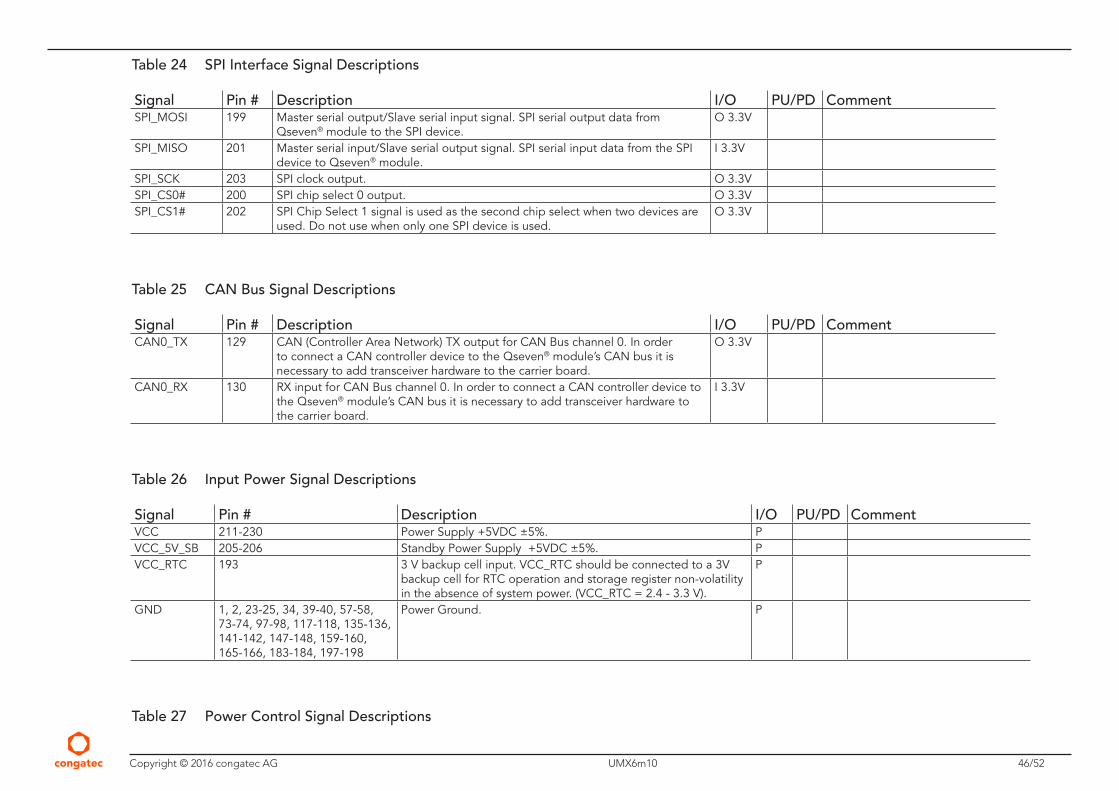
Copyright © 2016 congatec AG UMX6m10 46/52
Table 24 SPI Interface Signal Descriptions
Signal Pin # Description I/O PU/PD CommentSPI_MOSI 199 Master serial output/Slave serial input signal. SPI serial output data from
Qseven® module to the SPI device. O 3.3V
SPI_MISO 201 Master serial input/Slave serial output signal. SPI serial input data from the SPI device to Qseven® module.
I 3.3V
SPI_SCK 203 SPI clock output. O 3.3VSPI_CS0# 200 SPI chip select 0 output. O 3.3VSPI_CS1# 202 SPI Chip Select 1 signal is used as the second chip select when two devices are
used. Do not use when only one SPI device is used.O 3.3V
Table 25 CAN Bus Signal Descriptions
Signal Pin # Description I/O PU/PD CommentCAN0_TX 129 CAN (Controller Area Network) TX output for CAN Bus channel 0. In order
to connect a CAN controller device to the Qseven® module’s CAN bus it is necessary to add transceiver hardware to the carrier board.
O 3.3V
CAN0_RX 130 RX input for CAN Bus channel 0. In order to connect a CAN controller device to the Qseven® module’s CAN bus it is necessary to add transceiver hardware to the carrier board.
I 3.3V
Table 26 Input Power Signal Descriptions
Signal Pin # Description I/O PU/PD CommentVCC 211-230 Power Supply +5VDC ±5%. PVCC_5V_SB 205-206 Standby Power Supply +5VDC ±5%. PVCC_RTC 193 3 V backup cell input. VCC_RTC should be connected to a 3V
backup cell for RTC operation and storage register non-volatility in the absence of system power. (VCC_RTC = 2.4 - 3.3 V).
P
GND 1, 2, 23-25, 34, 39-40, 57-58, 73-74, 97-98, 117-118, 135-136, 141-142, 147-148, 159-160, 165-166, 183-184, 197-198
Power Ground. P
Table 27 Power Control Signal Descriptions

Copyright © 2016 congatec AG UMX6m10 47/52
Signal Pin # Description I/O PU/PD CommentPWGIN 26 High active input for the Qseven® module indicates that power from the power supply is
ready. I 5V PU 10k 5V
PWRBTN# 20 Power Button: Low active power button input. This signal is triggered on the falling edge. I 3.3VSB PU 10k 3.3V
Table 28 Power Management Signal Descriptions
Signal Pin # Description I/O PU/PD CommentRSTBTN# 28 Reset button input. This input may be driven active low by an external circuitry to reset
the Qseven® module.I 3.3V
BATLOW# 27 Battery low input. This signal may be driven active low by external circuitry to signal that the system battery is low or may be used to signal some other external battery management event.
I 3.3VSB Connected to GPIO
WAKE# 17 External system wake event. This may be driven active low by external circuitry to signal an external wake-up event.
I 3.3VSB
SUS_STAT# 19 Suspend Status: indicates that the system will be entering a low power state soon. Connected to GPIOSUS_S3# 18 S3 State: This signal shuts off power to all runtime system components that are not
maintained during S3 (Suspend to Ram), S4 or S5 states.The signal SUS_S3# is necessary in order to support the optional S3 cold power state.
O 3.3VSB Connected to PMIC and driven by the software via GPIO.
SUS_S5# 16 S5 State: This signal indicates S4 or S5 (Soft Off) state. O 3.3VSB Connected to PMICSLP_BTN# 21 Sleep button. Low active signal used by the ACPI operating system to transition the
system into sleep state or to wake it up again. This signal is triggered on falling edge.I 3.3VSB PU 10k
3.3VSBConnected to GPIO
LID_BTN# 22 LID button. Low active signal used by the ACPI operating system to detect a LID switch and to bring system into sleep state or to wake it up again.
I 3.3VSB PU 10k 3.3VSB
Connected to GPIO
Table 29 Miscellaneous Signal Descriptions
Signal Pin # Description I/O PU/PD CommentWDTRIG# 70 Watchdog trigger signal. This signal restarts the watchdog timer of the Qseven®
module on the falling edge of a low active pulse.I 3.3V Connected to GPIO
WDOUT 72 Watchdog event indicator. High active output used for signaling a missing watchdog trigger. Will be deasserted by software, system reset or a system power down.
O 3.3V Connected to GPIO
GP0_I2C_CLK 66 General Purpose I²C bus #0 clock line I/O 3.3V OD PU 4k7 3.3VGP0_I2C_DAT 68 General Purpose I²C bus #0 data line I/O 3.3V OD PU 4k7 3.3VGP1_I2C_CLK 60 Clock line of System Management Bus.
Multiplexed with General Purpose I²C bus #1 clock lineI/O 3.3VSB OD
PU 4k7 3.3V Connected to I2C
GP1_I2C_DAT 62 Data line of System Management Bus.Multiplexed with General Purpose I²C bus #1 data line
I/O 3.3VSB OD
PU 4k7 3.3V Connected to I2C
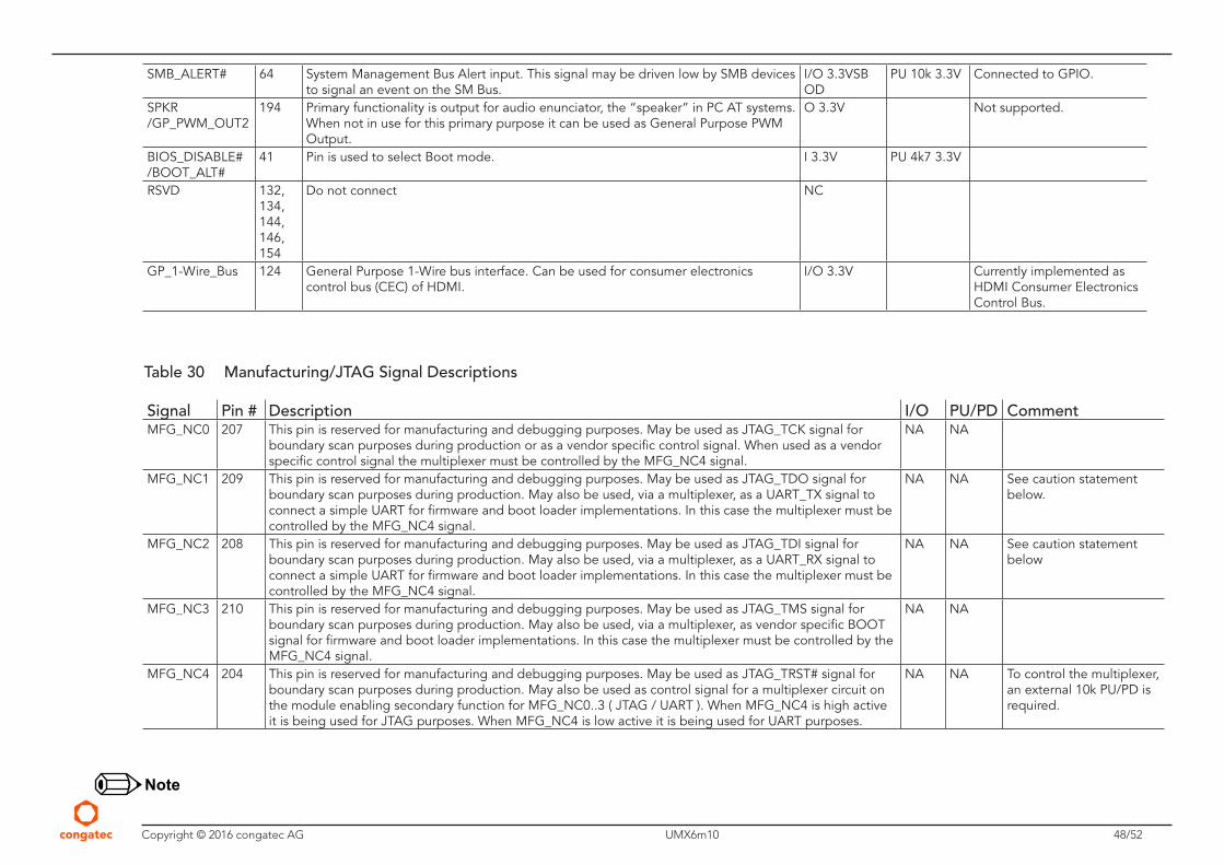
Copyright © 2016 congatec AG UMX6m10 48/52
SMB_ALERT# 64 System Management Bus Alert input. This signal may be driven low by SMB devices to signal an event on the SM Bus.
I/O 3.3VSB OD
PU 10k 3.3V Connected to GPIO.
SPKR/GP_PWM_OUT2
194 Primary functionality is output for audio enunciator, the “speaker” in PC AT systems. When not in use for this primary purpose it can be used as General Purpose PWM Output.
O 3.3V Not supported.
BIOS_DISABLE#/BOOT_ALT#
41 Pin is used to select Boot mode. I 3.3V PU 4k7 3.3V
RSVD 132, 134, 144, 146, 154
Do not connect NC
GP_1-Wire_Bus 124 General Purpose 1-Wire bus interface. Can be used for consumer electronics control bus (CEC) of HDMI.
I/O 3.3V Currently implemented as HDMI Consumer Electronics Control Bus.
Table 30 Manufacturing/JTAG Signal Descriptions
Signal Pin # Description I/O PU/PD CommentMFG_NC0 207 This pin is reserved for manufacturing and debugging purposes. May be used as JTAG_TCK signal for
boundary scan purposes during production or as a vendor specific control signal. When used as a vendor specific control signal the multiplexer must be controlled by the MFG_NC4 signal.
NA NA
MFG_NC1 209 This pin is reserved for manufacturing and debugging purposes. May be used as JTAG_TDO signal for boundary scan purposes during production. May also be used, via a multiplexer, as a UART_TX signal to connect a simple UART for firmware and boot loader implementations. In this case the multiplexer must be controlled by the MFG_NC4 signal.
NA NA See caution statement below.
MFG_NC2 208 This pin is reserved for manufacturing and debugging purposes. May be used as JTAG_TDI signal for boundary scan purposes during production. May also be used, via a multiplexer, as a UART_RX signal to connect a simple UART for firmware and boot loader implementations. In this case the multiplexer must be controlled by the MFG_NC4 signal.
NA NA See caution statement below
MFG_NC3 210 This pin is reserved for manufacturing and debugging purposes. May be used as JTAG_TMS signal for boundary scan purposes during production. May also be used, via a multiplexer, as vendor specific BOOT signal for firmware and boot loader implementations. In this case the multiplexer must be controlled by the MFG_NC4 signal.
NA NA
MFG_NC4 204 This pin is reserved for manufacturing and debugging purposes. May be used as JTAG_TRST# signal for boundary scan purposes during production. May also be used as control signal for a multiplexer circuit on the module enabling secondary function for MFG_NC0..3 ( JTAG / UART ). When MFG_NC4 is high active it is being used for JTAG purposes. When MFG_NC4 is low active it is being used for UART purposes.
NA NA To control the multiplexer, an external 10k PU/PD is required.
Note
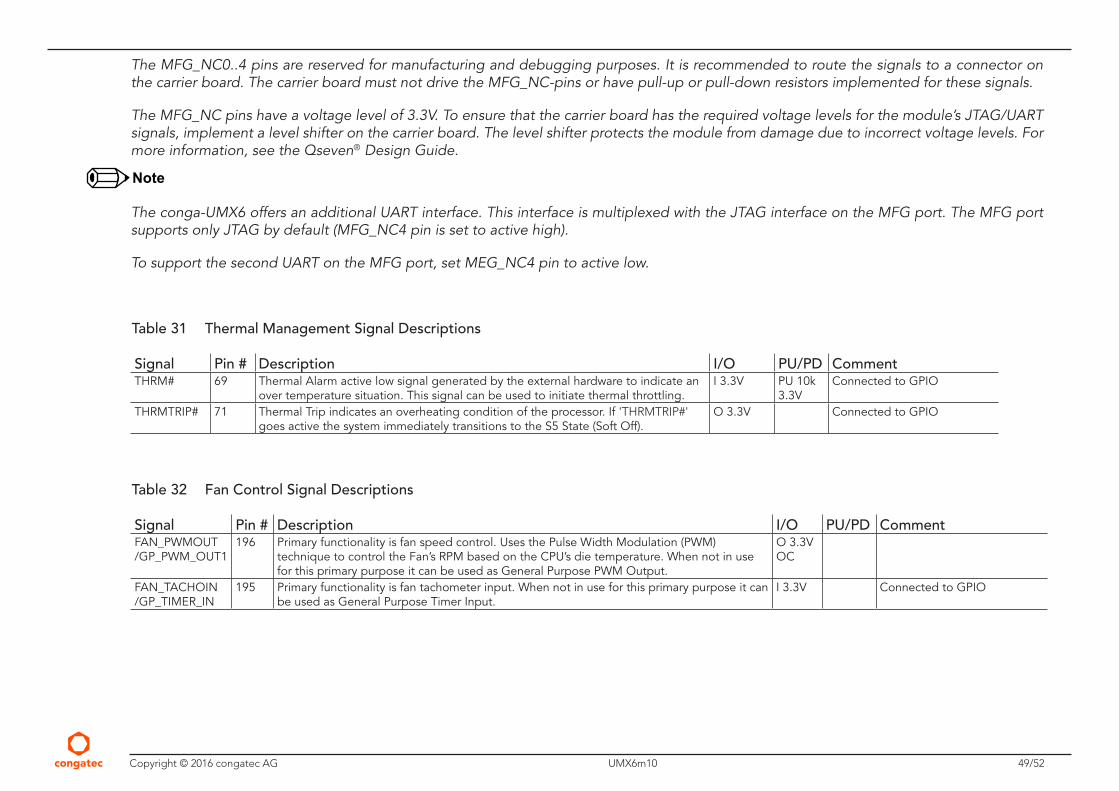
Copyright © 2016 congatec AG UMX6m10 49/52
The MFG_NC0..4 pins are reserved for manufacturing and debugging purposes. It is recommended to route the signals to a connector on the carrier board. The carrier board must not drive the MFG_NC-pins or have pull-up or pull-down resistors implemented for these signals.
The MFG_NC pins have a voltage level of 3.3V. To ensure that the carrier board has the required voltage levels for the module’s JTAG/UART signals, implement a level shifter on the carrier board. The level shifter protects the module from damage due to incorrect voltage levels. For more information, see the Qseven® Design Guide.
Note
The conga-UMX6 offers an additional UART interface. This interface is multiplexed with the JTAG interface on the MFG port. The MFG port supports only JTAG by default (MFG_NC4 pin is set to active high).
To support the second UART on the MFG port, set MEG_NC4 pin to active low.
Table 31 Thermal Management Signal Descriptions
Signal Pin # Description I/O PU/PD CommentTHRM# 69 Thermal Alarm active low signal generated by the external hardware to indicate an
over temperature situation. This signal can be used to initiate thermal throttling.I 3.3V PU 10k
3.3VConnected to GPIO
THRMTRIP# 71 Thermal Trip indicates an overheating condition of the processor. If 'THRMTRIP#' goes active the system immediately transitions to the S5 State (Soft Off).
O 3.3V Connected to GPIO
Table 32 Fan Control Signal Descriptions
Signal Pin # Description I/O PU/PD CommentFAN_PWMOUT/GP_PWM_OUT1
196 Primary functionality is fan speed control. Uses the Pulse Width Modulation (PWM) technique to control the Fan’s RPM based on the CPU’s die temperature. When not in use for this primary purpose it can be used as General Purpose PWM Output.
O 3.3V OC
FAN_TACHOIN/GP_TIMER_IN
195 Primary functionality is fan tachometer input. When not in use for this primary purpose it can be used as General Purpose Timer Input.
I 3.3V Connected to GPIO
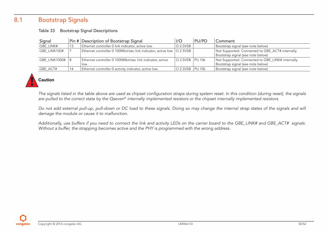
Copyright © 2016 congatec AG UMX6m10 50/52
8.1 Bootstrap Signals
Table 33 Bootstrap Signal Descriptions
Signal Pin # Description of Bootstrap Signal I/O PU/PD CommentGBE_LINK# 13 Ethernet controller 0 link indicator, active low. O 2.5VSB Bootstrap signal (see note below)GBE_LINK100# 7 Ethernet controller 0 100Mbit/sec link indicator, active low. O 2.5VSB Not Supported. Connected to GBE_ACT# internally.
Bootstrap signal (see note below)GBE_LINK1000# 8 Ethernet controller 0 1000Mbit/sec link indicator, active
low.O 2.5VSB PU 10k Not Supported. Connected to GBE_LINK# internally.
Bootstrap signal (see note below)GBE_ACT# 14 Ethernet controller 0 activity indicator, active low. O 2.5VSB PU 10k Bootstrap signal (see note below)
Caution
The signals listed in the table above are used as chipset configuration straps during system reset. In this condition (during reset), the signals are pulled to the correct state by the Qseven® internally implemented resistors or the chipset internally implemented resistors.
Do not add external pull-up, pull-down or DC load to these signals. Doing so may change the internal strap states of the signals and will damage the module or cause it to malfunction.
Additionally, use buffers if you need to connect the link and activity LEDs on the carrier board to the GBE_LINK# and GBE_ACT# signals. Without a buffer, the strapping becomes active and the PHY is programmed with the wrong address.
Copyright © 2016 congatec AG UMX6m10 51/52
9 Onboard Interfaces and Devices
9.1 SPI Flash
The conga-UMX6 has an onboard 32 Mbit SPI flash memory. This flash memory contains the bootloader and is directly connected to the ECSPI-1 interface of the i.MX6 processor.
The NXP® i.MX6 processor is programmed to boot from the SPI flash.
9.2 DDR3 Memory
The conga-UMX6 offers a 1GB DDR3 SDRAM memory onboard. The memory modules are connected directly to the DDR ports of the NXP® i.MX6 processor.
9.3 eMMC
The conga-UMX6 offers a 4G eMMC module onboard. The onboard eMMC is a nand flash device and it is routed directly to the SDIO port 3 of the NXP® i.MX6 processor. Eight lanes are used for data.

Copyright © 2016 congatec AG UMX6m10 52/52
10 Industry SpecificationsThe table below provides links to industry specifications that apply to congatec AG modules.
Table 34 References
Specification LinkQseven® Specification http://www.qseven-standard.org/Qseven® Design Guide http://www.qseven-standard.org/Low Pin Count Interface Specification, Revision 1.0 (LPC) http://developer.intel.com/design/chipsets/industry/lpc.
htmUniversal Serial Bus (USB) Specification, Revision 2.0 http://www.usb.org/homeSerial ATA Specification, Revision 1.0a http://www.serialata.orgPCI Express Base Specification, Revision 2.0 http://www.pcisig.com/specificationsNXP website http://www.NXP.com