construction electrician apprenticeship · pdf fileanalyze electronic circuits ... describe...
TRANSCRIPT

CONSTRUCTION ELECTRICIAN APPRENTICESHIP PROGRAMLevel 4 Line D: Apply Circuit Concepts
LEARNING GUIDE D-6ANALYZE ELECTRONIC CIRCUITS
D-6


ForewordThe Industry Training Authority (ITA) is pleased to release this major update of learning resources to support the delivery of the BC Electrician Apprenticeship Program. It was made possible by the dedicated efforts of the Electrical Articulation Committee of BC (EAC).
The EAC is a working group of electrical instructors from institutions across the province and is one of the key stakeholder groups that supports and strengthens industry training in BC. It was the driving force behind the update of the Electrician Apprenticeship Program Learning Guides, supplying the specialized expertise required to incorporate technological, procedural and industry-driven changes. The EAC plays an important role in the province’s post-secondary public institutions. As discipline specialists the committee’s members share information and engage in discussions of curriculum matters, particularly those affecting student mobility.
ITA would also like to acknowledge the Construction Industry Training Organization (CITO) which provides direction for improving industry training in the construction sector. CITO is responsible for organizing industry and instructor representatives within BC to consult and provide changes related to the BC Construction Electrician Training Program.
We are grateful to EAC for their contributions to the ongoing development of BC Construction Electrician Training Program Learning Guides (materials whose ownership and copyright are maintained by the Province of British Columbia through ITA).
Industry Training AuthorityJanuary 2011
DisclaimerThe materials in these Learning Guides are for use by students and instructional staff and have been compiled from sources believed to be reliable and to represent best current opinions on these subjects. These manuals are intended to serve as a starting point for good practices and may not specify all minimum legal standards. No warranty, guarantee or representation is made by the British Columbia Electrical Articulation Committee, the British Columbia Industry Training Authority or the Queen’s Printer of British Columbia as to the accuracy or sufficiency of the information contained in these publications. These manuals are intended to provide basic guidelines for electrical trade practices. Do not assume, therefore, that all necessary warnings and safety precautionary measures are contained in this module and that other or additional measures may not be required.

Acknowledgements and CopyrightCopyright © 2011, 2014 Industry Training Authority
All rights reserved. No part of this publication may be reproduced or transmitted in any form or by any means, electronic or digital, without written permission from Industry Training Authority (ITA). Reproducing passages from this publication by photographic, electrostatic, mechanical, or digital means without permission is an infringement of copyright law.
The issuing/publishing body is: Crown Publications, Queen’s Printer, Ministry of Citizens’ Services
The Industry Training Authority of British Columbia would like to acknowledge the Electrical Articulation Committee and Open School BC, the Ministry of Education, as well as the following individuals and organizations for their contributions in updating the Electrician Apprenticeship Program Learning Guides:
Electrical Articulation Committee (EAC) Curriculum SubcommitteePeter Poeschek (Thompson Rivers University)Ken Holland (Camosun College)Alain Lavoie (College of New Caledonia)Don Gillingham (North Island University)Jim Gamble (Okanagan College)John Todrick (University of the Fraser Valley) Ted Simmons (British Columbia Institute of Technology)
Members of the Curriculum Subcommittee have assumed roles as writers, reviewers, and subject matter experts throughout the development and revision of materials for the Electrician Apprenticeship Program.
Open School BCOpen School BC provided project management and design expertise in updating the Electrician Apprenticeship Program print materials:
Adrian Hill, Project ManagerEleanor Liddy, Director/SupervisorBeverly Carstensen, Dennis Evans, Laurie Lozoway, Production Technician (print layout, graphics)Christine Ramkeesoon, Graphics Media CoordinatorKeith Learmonth, EditorMargaret Kernaghan, Graphic Artist
Publishing Services, Queen’s PrinterSherry Brown, Director of QP Publishing Services
Intellectual Property Program Ilona Ugro, Copyright Officer, Ministry of Citizens’ Services, Province of British Columbia
To order copies of any of the Electrician Apprenticeship Program Learning Guide, please contact us:
Crown Publications, Queen’s PrinterPO Box 9452 Stn Prov Govt563 Superior Street 2nd FlrVictoria, BC V8W 9V7Phone: 250-387-6409Toll Free: 1-800-663-6105Fax: 250-387-1120Email: [email protected]: www.crownpub.bc.ca
Version 1Corrected, January 2017 Corrected, October 2015 Revised, December 2014 Revised, April 2014 New, October 2012
CONSTRUCTION ELECTRICIAN APPRENTICESHIP PROGRAM: LEVEL 4 5
LEVEL 4, LEARNING GUIDE D-6:
ANALYZE ELECTRONIC CIRCUITSLearning Objectives . . . . . . . . . . . . . . . . . . . . . . . . . . . . . . . . . . . . . . . . . . . . . . . 7
Learning Task 1: Describe common number systems used in digital electronics . . . . . . . . . . 9Self-Test 1. . . . . . . . . . . . . . . . . . . . . . . . . . . . . . . . . . . . . . . . . 24
Learning Task 2: Describe the operation of common logic gates . . . . . . . . . . . . . . . . . . 27Self-Test 2. . . . . . . . . . . . . . . . . . . . . . . . . . . . . . . . . . . . . . . . . 36
Learning Task 3: Describe Boolean algebra . . . . . . . . . . . . . . . . . . . . . . . . . . . . . . . 39Self-Test 3. . . . . . . . . . . . . . . . . . . . . . . . . . . . . . . . . . . . . . . . . 50
Learning Task 4: Describe the operation of special combination logic circuits . . . . . . . . . . 53Self-Test 4. . . . . . . . . . . . . . . . . . . . . . . . . . . . . . . . . . . . . . . . . 80
Learning Task 5: Describe the features of integrated circuits (IC) . . . . . . . . . . . . . . . . . . 85Self-Test 5. . . . . . . . . . . . . . . . . . . . . . . . . . . . . . . . . . . . . . . . . 94
Learning Task 6: Connect and test digital logic circuits . . . . . . . . . . . . . . . . . . . . . . . . 97Self-Test 6. . . . . . . . . . . . . . . . . . . . . . . . . . . . . . . . . . . . . . . . .100
Learning Task 7: Describe the features of operational amplifiers . . . . . . . . . . . . . . . . . .101Self-Test 7. . . . . . . . . . . . . . . . . . . . . . . . . . . . . . . . . . . . . . . . .107
Learning Task 8: Describe common circuit applications for the operational amplifier . . . . .109Self-Test 8. . . . . . . . . . . . . . . . . . . . . . . . . . . . . . . . . . . . . . . . .118
Answer Key . . . . . . . . . . . . . . . . . . . . . . . . . . . . . . . . . . . . . . . . . . . . . . . . . .121

6 CONSTRUCTION ELECTRICIAN APPRENTICESHIP PROGRAM: LEVEL 4

LEARNING ObjECTIVES D-6
CONSTRUCTION ELECTRICIAN APPRENTICESHIP PROGRAM: LEVEL 4 7
Learning Objectives• The learner will be able to analyze electronic circuits that utilize logic gates.
• The learner will be able to describe the operating principles of op-amps.
• The learner will be able to analyze electronic circuits that utilize op-amps.
• The learner will be able to describe the operating principles of logic gates.
• The learner will be able to convert between numbering systems.
• The learner will be able to describe coding and decoding information.
Activities• Read and study the topics of Learning Guide D-6: Analyze Electronic Circuits.
• Complete Self-Tests 1 through 8. Check your answers with the Answer Key provided at the end of this Learning Guide.
Resources
All resources are provided in this Learning Guide.

8 CONSTRUCTION ELECTRICIAN APPRENTICESHIP PROGRAM: LEVEL 4
BC Trades Moduleswww.bctradesmodules.ca
We want your feedback! Please go the BC Trades Modules website to enter comments about specific section(s) that require correction or modification. All submissions will be reviewed and considered for inclusion in the next revision.
SAFETY ADVISORYBe advised that references to the Workers’ Compensation Board of British Columbia safety regulations contained within these materials do not/may not reflect the most recent Occupational Health and Safety Regulation. The current Standards and Regulation in BC can be obtained at the following website: http://www.worksafebc.com.
Please note that it is always the responsibility of any person using these materials to inform him/herself about the Occupational Health and Safety Regulation pertaining to his/her area of work.
Industry Training Authority January 2011
CONSTRUCTION ELECTRICIAN APPRENTICESHIP PROGRAM: LEVEL 4 9
Learning Task 1:
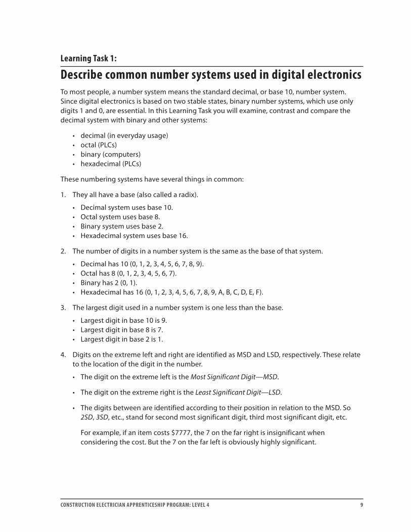
Describe common number systems used in digital electronicsTo most people, a number system means the standard decimal, or base 10, number system. Since digital electronics is based on two stable states, binary number systems, which use only digits 1 and 0, are essential. In this Learning Task you will examine, contrast and compare the decimal system with binary and other systems:
• decimal (in everyday usage)• octal (PLCs)• binary (computers)• hexadecimal (PLCs)
These numbering systems have several things in common:
1. They all have a base (also called a radix).
• Decimal system uses base 10.• Octal system uses base 8.• Binary system uses base 2.• Hexadecimal system uses base 16.
2. The number of digits in a number system is the same as the base of that system.
• Decimal has 10 (0, 1, 2, 3, 4, 5, 6, 7, 8, 9).• Octal has 8 (0, 1, 2, 3, 4, 5, 6, 7).• Binary has 2 (0, 1).• Hexadecimal has 16 (0, 1, 2, 3, 4, 5, 6, 7, 8, 9, A, B, C, D, E, F).
3. The largest digit used in a number system is one less than the base.
• Largest digit in base 10 is 9.• Largest digit in base 8 is 7.• Largest digit in base 2 is 1.
4. Digits on the extreme left and right are identified as MSD and LSD, respectively. These relate to the location of the digit in the number.
• The digit on the extreme left is the Most Significant Digit—MSD.
• The digit on the extreme right is the Least Significant Digit—LSD.
• The digits between are identified according to their position in relation to the MSD. So 2SD, 3SD, etc., stand for second most significant digit, third most significant digit, etc.
For example, if an item costs $7777, the 7 on the far right is insignificant when considering the cost. But the 7 on the far left is obviously highly significant.

LEARNING TASk 1 D-6
10 CONSTRUCTION ELECTRICIAN APPRENTICESHIP PROGRAM: LEVEL 4
5. Numbers within a particular system are often identified by means of a subscript. For example:
• octal 12558
• hexadecimal 125516
Decimal systemThe most common numbering system, is the decimal system which uses base 10. (The decimal system and the base 10 system are one and the same.) The decimal system has 10 digits, of which the highest digit is 9. If a number is written without showing a subscript base, base 10 is implied. Thus, the number 256 = 25610.
Example 1: The following equation explains what 25610 or 256 means:
256 2 10 5 10 6 10
2 100 5 10 6
102 1 0= × + × + ×
= × + × +
( ) ( ) ( )
( ) ( ) ( ××
= + +
1
200 50 6
)
In other words, there are two 100s, five 10s and six 1s in the number 256.
A number raised to the power of zero equals 1. Therefore: 100 = 1, 80 = 1, 160 = 1, and so on.
Example 2: What does 647910 or 6479 mean?
6479 6 10 4 10 7 10 9 10
6 1000
103 2 1 0= × + × + × + ×
= ×
( ) ( ) ( ) ( )
( ) ++ × + × + ×
= + + +
=
( ) ( ) ( )4 100 7 10 9 1
6000 400 70 9
6479
This shows that there are six 1000s, four 100s, seven 10s, and nine 1s in the number 6479.
All you are doing with a base 10 number is multiplying the LSD by 100, the next digit by 101, the next digit by 102, and so on, up to and including the MSD.
Octal systemThe octal system uses base 8. This means that it has 8 digits, the highest of which is 7. Notice in the following examples that the octal number is treated in the same way as the decimal, except here you are using 8 instead of 10. The LSD is multiplied by 80, the next digit by 81, the next by 82, and so on to the left, until you reach the last digit.
LEARNING TASk 1 D-6
CONSTRUCTION ELECTRICIAN APPRENTICESHIP PROGRAM: LEVEL 4 11
Example 1: What does the number 2568 equal in the base 10, or decimal, system?
256 2 8 5 8 6 8
2 64 5 8 6 1
12
82 1 0= × + × + ×
= × + × + ×
=
( ) ( ) ( )
( ) ( ) ( )
88 40 6+ +
Thus 2568 = 17410 (or simply 174). This would be stated: Two-five-six octal equals one-hundred-seventy-four.
Example 2: What is 648 in decimal?
64 6 8 4 8
6 8 4 1
48 4
52
81 0= × + ×
= × + ×
= +
=
( ) ( )
( ) ( )
Example 3: What is 4328 in decimal?
432 4 8 3 8 2 8
4 64 3 8 2 1
25
82 1 0= × + × + ×
= × + × + ×
=
( ) ( ) ( )
( ) ( ) ( )
66 24 2
282
+ +
=
Example 4: What is 12348 in decimal?
1234 1 8 2 8 3 8 4 8
1 512 2 64
83 2 1 0= × + × + × + ×
= × + ×
( ) ( ) ( ) ( )
( ) ( )) ( ) ( )+ × + ×
= + + +
=
3 8 4 1
512 128 24 4
668
Binary systemThe binary system uses base 2. This means it has 2 digits, the highest of which is 1. You will find only 0s and 1s in a binary number. Notice in the following examples the symmetry to the decimal and octal system. Binary uses base 2, so here we are using 2 instead of the 8 and 10 previously used in octal and base 10, respectively. The LSD is multiplied by 20, the next digit by 21, the next by 22, and so on to the left, until you reach the MSD.

LEARNING TASk 1 D-6
12 CONSTRUCTION ELECTRICIAN APPRENTICESHIP PROGRAM: LEVEL 4
Example 1: What does the binary number 10112 equal in decimal?
1011 1 2 0 2 1 2 1 2
1 8 0 4
23 2 1 0= × + × + × + ×
= × + × +
( ) ( ) ( ) ( )
( ) ( ) (11 2 1 1
8 0 2 1
11
× + ×
= + + +
=
) ( )
Therefore 10112 = 1110 , or 11, or “eleven.”
Example 2: What is 11 1002 in decimal?
11100 1 2 1 2 1 2 0 2 0 2
1 16
24 3 2 1 0= × + × + × + × + ×
= ×
( ) ( ) ( ) ( ) ( )
( )) ( ) ( ) ( ) ( )+ × + × + × + ×
= + + + +
=
1 8 1 4 0 2 0 1
16 8 4 0 0
28
Example 3: What is 10 1012 in decimal?
10 101 1 2 0 2 1 2 0 2 1 2
1 16
24 3 2 1 0= × + × + × + × + ×
= ×
( ) ( ) ( ) ( ) ( )
( )) ( ) ( ) ( ) ( )+ × + × + × + ×
= + + + +
=
0 8 1 4 0 2 1 1
16 0 4 0 1
21
Another method of converting binary to decimalIf we consider a binary number, 111 112, the LSD represents 1(20), the next represents 2 (21), the next is 4 (22), the next is 8 (23), and the last, the MSD, is 16 (24). Starting with the LSD = 1, (or LSB for lowest significant bit, as it is more commonly called), the numbers represented by the 1s in binary keep doubling: 2, 4, 8, 16, 32, 64, 128, 256 and so on, as you move towards the MSB. These decimal digits are then added up to give the decimal equivalent of the binary.
If there is a 0 in the binary number it merely means the absence of one of these numbers. Therefore if you want to find the decimal equivalent of a binary number you can find it by the method shown in the following example.
Example 1: Change 11001112 to decimal.
Note that you stroke out the numbers represented by the 0s and add the others.
1 1 0 0 1 1 1↓ ↓ ↓ ↓ ↓ ↓ ↓
64 + 32 + 16 + 8 + 4 + 2 + 1 = 103
Therefore: 11001012 = 103

LEARNING TASk 1 D-6
CONSTRUCTION ELECTRICIAN APPRENTICESHIP PROGRAM: LEVEL 4 13
Example 2: Change 10111002 to decimal
1 0 1 1 1 0 0↓ ↓ ↓ ↓ ↓ ↓ ↓
64 + 32 + 16 + 8 + 4 + 2 + 1 = 92
Therefore: 10111002 = 92
Hexadecimal systemThe hexadecimal system uses base 16. It has 16 digits, the highest of which is decimal 15. Because decimal numbers 10 to 15 require two digits each, you will see letters as well as numbers in a hexadecimal number. Letters A, B, C, D, E and F replace numbers 10, 11, 12, 13, 14 and 15, respectively. The hexadecimal number is treated exactly like numbers with other bases. In the following examples you use 16 instead of the 2, 8 and 10 for binary, octal and decimal, respectively. The LSD is multiplied by 160, the next digit by 161, the next by 162, and so on to the left, until you reach the last digit.
Example 1: What does 25616 equal in decimal?
256 2 16 5 16 6 16
2 256 5 16 6
162 1 0= × + × + ×
= × + × +
( ) ( ) ( )
( ) ( ) ( ××
= + +
=
1
512 80 6
598
)
Therefore: 25616 = 59810, or simply, 598.
Example 2: What does 3C216 equal in decimal? (Note: C = 12)
3 2 3 16 12 16 2 16
3 256 12 16
162 1 0C = × + × + ×
= × + × +
( ) ( ) ( )
( ) ( ) (( )2 1
768 192 2
962
×
= + +
=
Therefore: 3C216 = 96210, or simply, 962.
Example 3: What does 12AB16 equal in decimal? (Note: A = 10, B = 11)
12 1 16 2 16 10 16 11 16
1 409
163 2 1 0AB = × + × + × + ×
= ×
( ) ( ) ( ) ( )
( 66 2 256 10 16 11 1
4096 512 160 11
4779
) ( ) ( ) ( )+ × + × + ×
= + + +
=
LEARNING TASk 1 D-6
14 CONSTRUCTION ELECTRICIAN APPRENTICESHIP PROGRAM: LEVEL 4
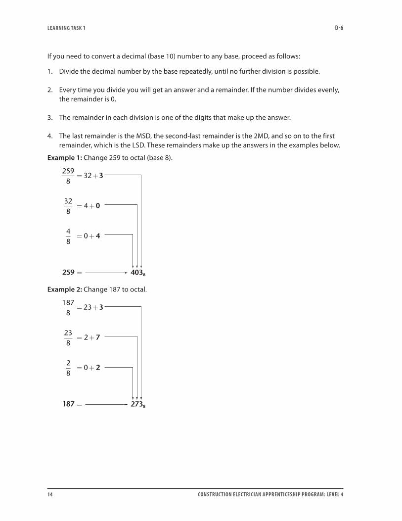
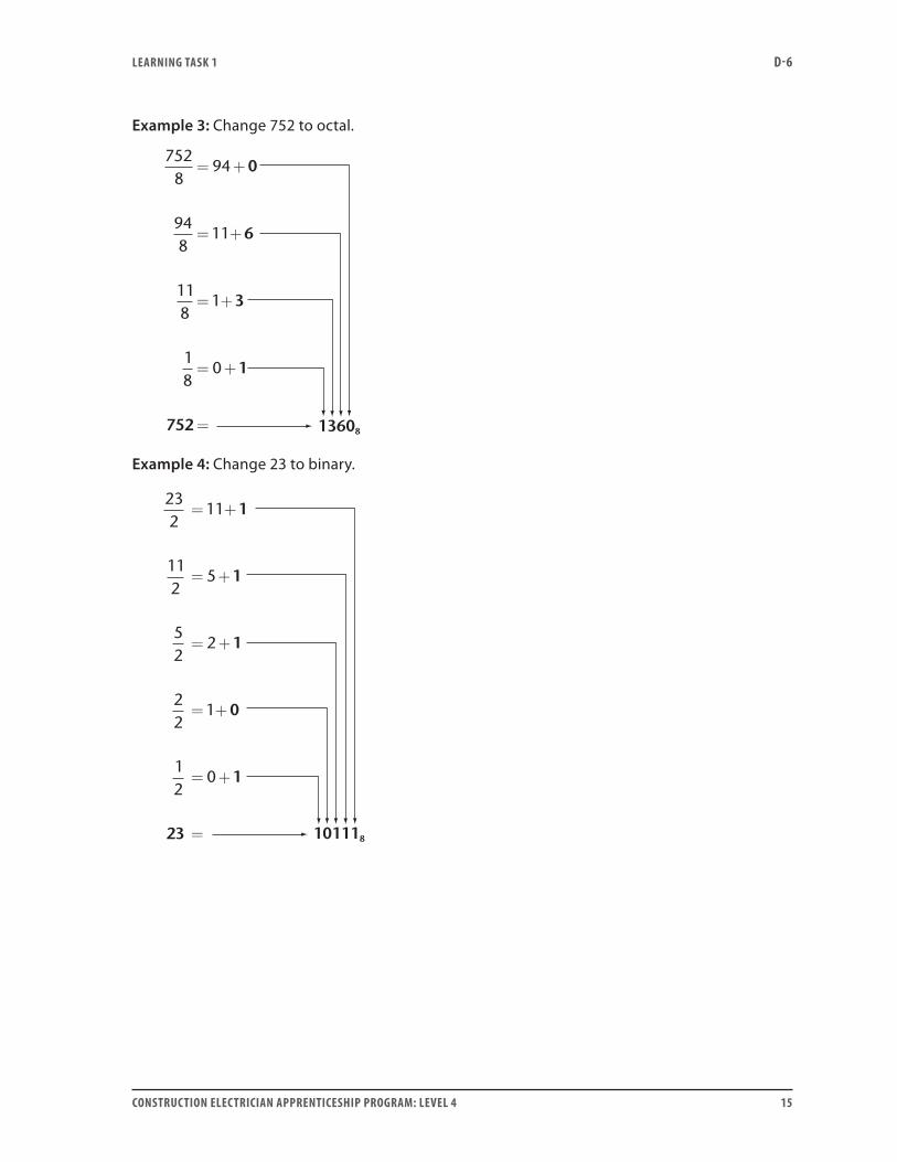
If you need to convert a decimal (base 10) number to any base, proceed as follows:
1. Divide the decimal number by the base repeatedly, until no further division is possible.
2. Every time you divide you will get an answer and a remainder. If the number divides evenly, the remainder is 0.
3. The remainder in each division is one of the digits that make up the answer.
4. The last remainder is the MSD, the second-last remainder is the 2MD, and so on to the first remainder, which is the LSD. These remainders make up the answers in the examples below.
Example 1: Change 259 to octal (base 8).
2598
32 3
328
4 0
48
0 4
259
= +
= +
= +
= 4038
Example 2: Change 187 to octal.
1878
23 3
238
2 7
28
0 2
187
= +
= +
= +
= 2738
LEARNING TASk 1 D-6
CONSTRUCTION ELECTRICIAN APPRENTICESHIP PROGRAM: LEVEL 4 15
Example 3: Change 752 to octal.
13608
7528
94 0
948
11 6
118
1 3
18
0 1
752
= +
= +
= +
= +
=
Example 4: Change 23 to binary.
101118
232
11 1
112
5 1
52
2 1
22
1 0
12
0 1
23
= +
= +
= +
= +
= +
=

LEARNING TASk 1 D-6
16 CONSTRUCTION ELECTRICIAN APPRENTICESHIP PROGRAM: LEVEL 4
Example 5: Change 74 to binary.
10010102
742
37 0
372
18 1
182
9 0
92
4 1
42
2 0
22
1 0
12
0 1
= +
= +
= +
= +
= +
= +
= +
774 =
Example 6: Change 1325 to hexadecimal.
52D16
132516
82 13
8216
5 2
516
0 5
1325
= +
= +
= +
=

LEARNING TASk 1 D-6
CONSTRUCTION ELECTRICIAN APPRENTICESHIP PROGRAM: LEVEL 4 17
Example 7: Change 1767 to hexadecimal.
6E716
176716
110 7
11016
6 14
616
0 6
1767
= +
= +
= +
=
Example 8: Change 656 to hexadecimal.
29016
65616
41 0
4116
2 9
216
0 2
656
= +
= +
= +
=
Binary-to-Octal conversionsConverting Binary to OctalThe largest digit in the octal system is 78, which converted to binary is equal to 1112. From this we can see that it takes three binary bits to equal the largest digit in the octal system. To convert from binary to octal, starting at the LSD, separate the binary digits into groups of three.
Example 1: Change 00111011100111012 to its equivalent in octal.
011 101 110 011 101
3 5 6 3 5
00111011100111012 = 356358
Example 2: Change 110100101100012 from binary to octal. Zeros are added to the MSD to complete the final group if it is less than three digits
011 010 010 110 001
3 2 2 6 1
110100101100012 = 322618

LEARNING TASk 1 D-6
18 CONSTRUCTION ELECTRICIAN APPRENTICESHIP PROGRAM: LEVEL 4
Converting Octal to BinaryThe above procedure may be reversed if you need to convert octal to binary. Substitute the three bit binary equivalent, for each of the octal digits.
Example 1: Change 45678 to binary.
4 5 6 7
100 101 110 111
45678 = 1001011101112
Example 2: Change 76548 to binary.
7 6 5 4
111 110 101 100
76548 = 1111101011002
Binary-to-hexadecimal conversionThe procedure used to convert from binary to hexadecimal and vice-versa is very similar to that used in the binary-octal conversion, except that here groups of four bits must be used, because hexadecimal numbers go as high as F (or 15), which is 11112 in binary.
Example 1: Change 00111011100111012 to its equivalent in hexadecimal.
0011 1011 1001 1101
3 B 9 D
00111011100111012 = 3B9D16
As in the binary to octal conversion, zeros may have to be added to the MSD to complement the final grouping.
Example 2: Change 110100101100012 to hexadecimal.
11 0100 1011 0001
0011 0100 1011 0001
3 4 B 1
110100101100012 = 34B116
Converting hexadecimal to binaryThe above procedure may be reversed if you need to convert hexadecimal to binary. Substitute four bits for each of the hexadecimal digits.
Example: Change B06916 to binary.
B 0 6 9
1011 0000 0110 1001
B06916 = 10110000011010012

LEARNING TASk 1 D-6
CONSTRUCTION ELECTRICIAN APPRENTICESHIP PROGRAM: LEVEL 4 19
Binary-coded-decimal (BCD)You saw how a decimal number can be represented as a binary number. Consider the string of 1s and 0s as a code representing decimal numbers. When the binary equivalent of a decimal digit is substituted for that digit it is called encoding.
Conversions between decimal and binary can become unwieldy for large numbers. The BCD was designed as another method of representing decimal numbers in binary digits. BCD is used wherever decimal information is transferred in or out of a digital system. Such applications include calculators, digital electric meters and digital clocks. The chief advantage of BCD is the relative ease of conversion to and from decimal.
All digital systems must use some form of binary in their internal operation. A decimal like 12, or 11002, is seen by the computer as a sequence of highs and lows that correspond to the binary numbers, thus: “high,” “high,” “low,” “low.”
BCD is not used in contemporary computers because any given number requires more BCD bits than straight bits and this would reduce the speed of computer operation.
Converting decimal to BCDIn BCD, a four-bit code is used to represent each digit of a decimal number. Therefore, to change a decimal number into BCD you replace each of the decimal digits with four binary bits.
It is necessary to use four because, whereas digits 0 to 7 need only three bits, 8 and 9 require four bits, which are 1000 and 1001, respectively.
Example 1: Convert 568 to BCD.
5 = 01012
6 = 01102
8 = 10002
568 = 0101 0110 1000BCD
Decimal converted to BCD is not a binary number. Do not forget to use the subscript BCD to distinguish this from a binary number. The binary equivalent of 568 equals 10001110002, obviously not the same as the BCD group.
Example 2: Change 1769 to BCD.
1 7 6 9↓ ↓ ↓ ↓
0001 0111 0110 1001
Therefore: 1769 = 0001 0111 0110 1001BCD
Since the spacing between the groups is not necessary, it is written: 0001011101101001BCD
LEARNING TASk 1 D-6
20 CONSTRUCTION ELECTRICIAN APPRENTICESHIP PROGRAM: LEVEL 4
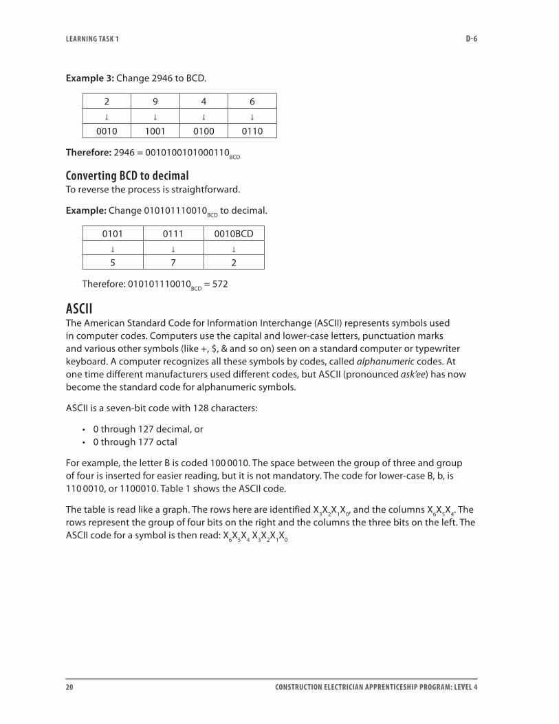
Example 3: Change 2946 to BCD.
2 9 4 6↓ ↓ ↓ ↓
0010 1001 0100 0110
Therefore: 2946 = 0010100101000110BCD
Converting BCD to decimalTo reverse the process is straightforward.
Example: Change 010101110010BCD to decimal.
0101 0111 0010BCD↓ ↓ ↓
5 7 2
Therefore: 010101110010BCD = 572
ASCIIThe American Standard Code for Information Interchange (ASCII) represents symbols used in computer codes. Computers use the capital and lower-case letters, punctuation marks and various other symbols (like +, $, & and so on) seen on a standard computer or typewriter keyboard. A computer recognizes all these symbols by codes, called alphanumeric codes. At one time different manufacturers used different codes, but ASCII (pronounced ask’ee) has now become the standard code for alphanumeric symbols.
ASCII is a seven-bit code with 128 characters:
• 0 through 127 decimal, or• 0 through 177 octal
For example, the letter B is coded 100 0010. The space between the group of three and group of four is inserted for easier reading, but it is not mandatory. The code for lower-case B, b, is 110 0010, or 1100010. Table 1 shows the ASCII code.
The table is read like a graph. The rows here are identified X3X2X1X0, and the columns X6X5X4. The rows represent the group of four bits on the right and the columns the three bits on the left. The ASCII code for a symbol is then read: X6X5X4 X3X2X1X0

LEARNING TASk 1 D-6
CONSTRUCTION ELECTRICIAN APPRENTICESHIP PROGRAM: LEVEL 4 21
Table 1: ASCII code
X3X2X1X0 X6X5X4
010 011 100 101 110 111
0000 SP 0 @ P p
0001 ! 1 A Q a q
0010 “ 2 B R b r
0011 # 3 C S c s
0100 $ 4 D T d t
0101 % 5 E U e u
0110 & 6 F V f v
0111 ’ 7 G W g w
1000 ( 8 H X h x
1001 ) 9 I Y i y
1010 * : J Z j z
1011 + ; K k
1100 , < L l
1101 - = M m
1110 . > N n
1111 / ? O o
Example 1: Take the letter B. This shows its column location as 100 and its row location as 0010. The letter B is therefore 100 0010.
Example 2: If we consider the word STOP typed on a computer keyboard, it would be encoded in ASCII as: 1010011101010010011111010000
S = 101 0011 T = 101 0100 O = 100 1111 P = 101 0000
Example 3: What does the encoded ASCII message: 010 0100 011 0010 011 0101 say?
010 0100 = $ 011 0010 = 2 011 0101 = 5
Therefore, it says $25.

LEARNING TASk 1 D-6
22 CONSTRUCTION ELECTRICIAN APPRENTICESHIP PROGRAM: LEVEL 4
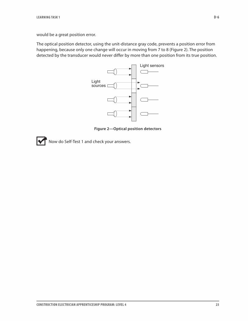
Gray codeThe gray code is one of a series of cyclic or “reflected” codes and is primarily used for positioning transducers. It is a four-bit code, but the bit positions do not have any weight attached to them, so the gray code is not used for arithmetic applications. The gray code for decimal numbers is shown in Table 2.
A characteristic of the gray code is that in going from one number to the consecutive number there is only a one-bit change.
Example: In Table 2 you will note that 7 = 0100 and 8 = 1100. Only one bit, the first one, has changed. Compare this to straight binary where 7 = 0111 and 8 = 1000. Here all four bits change. Simplicity is the main reason for the gray code.
Unit-distance measurementThe gray code is also called a unit-distance code. It is used in instrumentation where linear or angular displacement is measured. In such systems, transducers are used to monitor displacements and to produce bit values proportional to the linear or angular position.
Figure 1 shows a 16-segment shaft encoder of the gray code variety used to measure angular displacement as a disk rotates. The disk has 16 pie-shaped segments and shaded and unshaded windows in each segment. Shaded windows block light and unshaded windows let the light through. Optical sensors behind the disk produce a “1” for presence of light and a “0” for absence of light.
The pattern of shaded and unshaded windows in the disk produces the string of four bits that make up the gray code. The optical sensor will be in a fixed position to detect positional changes. For example, if the shaft is rotated with position 7 in line with the sensor, the optical sensor will register 0100 (no light, light, no light, no light).
There is only a one-bit change in going from one number to the next in the gray code. If, for example, the code on the shaft encoder were straight binary and the shaft at position 7, it would indicate 0111. If it then were to move to position 8, all four bits would have to change to 1000. But what if the disk were to stop between 7 and 8? Now the bit on the extreme left would change from 0 to 1 before the remaining three bits would change from 1s to 0s. The binary code would then appear as 1111, which is 15. This
Table 2: Gray code
Decimal Gray code0 00001 00012 00113 00104 01105 01116 01017 01008 11009 1101
10 111111 111012 101013 101114 100115 1000
Figure 1—Shaft encoder
LEARNING TASk 1 D-6
CONSTRUCTION ELECTRICIAN APPRENTICESHIP PROGRAM: LEVEL 4 23
would be a great position error.
The optical position detector, using the unit-distance gray code, prevents a position error from happening, because only one change will occur in moving from 7 to 8 (Figure 2). The position detected by the transducer would never differ by more than one position from its true position.
Lightsources
Light sensors
Figure 2—Optical position detectors
Now do Self-Test 1 and check your answers.

LEARNING TASk 1 D-6
24 CONSTRUCTION ELECTRICIAN APPRENTICESHIP PROGRAM: LEVEL 4
Self-Test 1Calculators are not to be used.
1. Identify the bases for the decimal, binary, octal and hexadecimal number systems.
2. Convert the following numbers to decimal:
a. 338
b. 4248
c. 17508
d. 111368
e. 234328
3. Convert the following numbers to decimal:
a. 11112
b. 1012
c. 100112
d. 111002
e. 101012

LEARNING TASk 1 D-6
CONSTRUCTION ELECTRICIAN APPRENTICESHIP PROGRAM: LEVEL 4 25
4. Convert the following hexadecimal numbers to decimal.
a. 2116
b. 11416
c. 3E716
d. 125D16
e. 17BB16
5. Convert the following decimal numbers to binary:
a. 46
b. 77
c. 27
6. Convert the following decimal numbers to hexadecimal:
a. 423
b. 214
c. 114
7. Convert the following binary number to hexadecimal:
10010110000010112
8. Convert the following octal number to binary: 13768
9. A BCD number and a straight binary number are one and the same.
a. true
b. false
10. Convert 1984 to BCD.

LEARNING TASk 1 D-6
26 CONSTRUCTION ELECTRICIAN APPRENTICESHIP PROGRAM: LEVEL 4
11. What is 0010 0100 1000BCD in decimal?
12. Because it represents both numbers and letters, ASCII is classified as an code.
13. What do the letters ASCII stand for?
14. Using Table 1 in the Learning Task, what ASCII code represents the letter M?
15. What is the unique feature of the gray code with respect to consecutive number representation?
Go to the Answer Key at the end of the Learning Guide to check your answers.
CONSTRUCTION ELECTRICIAN APPRENTICESHIP PROGRAM: LEVEL 4 27
Learning Task 2:
Describe the operation of common logic gatesA logic gate is a device with high-speed switching capability. Gates are made from integrated circuits, commonly called “ICs.” Logic gates are the electronic equivalent of mechanical switches connected in series or parallel. They are decision-making circuits. By combining logic gates, memory circuits can also be formed. The transistors, resistors and diodes that make up the typical logic gate are etched out of silicon. Although you need not be too concerned about the internal circuitry of a gate, you must know what to expect at an output for given inputs.
Typical logic gates are provided with two or more inputs and one output. They are designed to either block or pass digital signals. There are five basic logic gates:
• AND• OR• NOT (also called the inverter gate)• NAND• NOR
To fully understand digital electronics you must be conversant with these five basic gates.
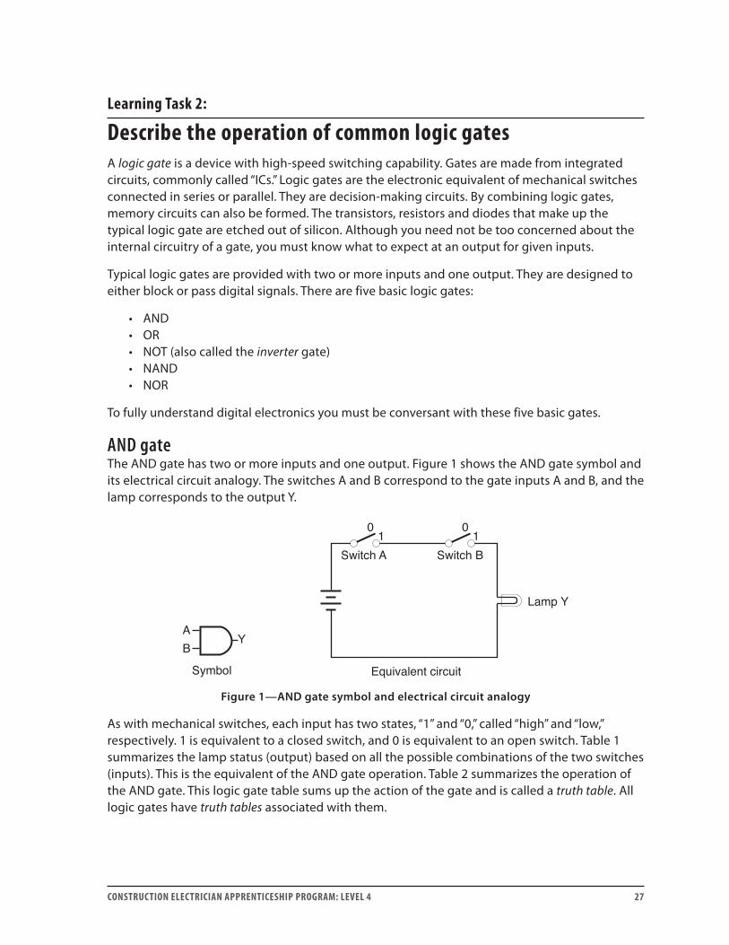
AND gateThe AND gate has two or more inputs and one output. Figure 1 shows the AND gate symbol and its electrical circuit analogy. The switches A and B correspond to the gate inputs A and B, and the lamp corresponds to the output Y.
Switch A Switch B
01
AB
Y
Symbol Equivalent circuit
Lamp Y
01
Figure 1—AND gate symbol and electrical circuit analogy
As with mechanical switches, each input has two states, “1” and “0,” called “high” and “low,” respectively. 1 is equivalent to a closed switch, and 0 is equivalent to an open switch. Table 1 summarizes the lamp status (output) based on all the possible combinations of the two switches (inputs). This is the equivalent of the AND gate operation. Table 2 summarizes the operation of the AND gate. This logic gate table sums up the action of the gate and is called a truth table. All logic gates have truth tables associated with them.

LEARNING TASk 2 D-6
28 CONSTRUCTION ELECTRICIAN APPRENTICESHIP PROGRAM: LEVEL 4
Table 1: Lamp status Table 2: AND truth table
Switch A Switch B Lamp Y Input A Input B Output Yoff off Off 0 0 0off on Off 0 1 0on off Off 1 0 0on on On 1 1 1
The lines in the truth table sum up the operation of the AND gate. Only when all the inputs to an AND gate are high (1) will you get a high (1) output. The gate is appropriately named AND since input A and input B must be 1 in order to get an output 1. Although AND gates are available with several inputs, the rule remains the same: all inputs must be high in order to obtain an output high. This is the same as with the equivalent switching circuit: all switches must be closed for the lamp to light.
Inputs and outputs 1 and 0 represent voltage levels. Typical nominal voltage levels would be +5 V and 0 V, respectively. It would be totally incorrect to assume 0 means the absence of a signal: 0, or low, is a very definite signal.
Boolean expressionA Boolean expression is a way of expressing the operation of a logic gate. For the AND gate, with inputs A and B and output Y, it is expressed: A • B = Y. The dot is taken to mean “and.” It may sometimes be omitted, and the expression, meaning the same thing, may be written as:
AB = Y
Boolean expressions (named after George Boole, an Irish mathematician) convey the gate operation: when A and B are high, C (Y) is high. If an AND gate had three inputs A, B and C, its Boolean expression would be: A • B • C = Y. Again, this may written ABC = Y to convey, mathematically, the gate operation. An AND gate with any number of inputs is written similarly.
The behaviour of any AND gate may be expressed by the statement Any low gives a low. This means that if any one of the inputs is 0, the output will be low.
LEARNING TASk 2 D-6
CONSTRUCTION ELECTRICIAN APPRENTICESHIP PROGRAM: LEVEL 4 29
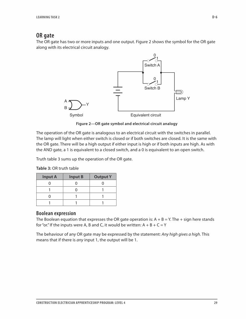
OR gateThe OR gate has two or more inputs and one output. Figure 2 shows the symbol for the OR gate along with its electrical circuit analogy.
Switch A
AB
Y
Symbol Equivalent circuit
01
Lamp Y
Switch B
01
Figure 2—OR gate symbol and electrical circuit analogy
The operation of the OR gate is analogous to an electrical circuit with the switches in parallel. The lamp will light when either switch is closed or if both switches are closed. It is the same with the OR gate. There will be a high output if either input is high or if both inputs are high. As with the AND gate, a 1 is equivalent to a closed switch, and a 0 is equivalent to an open switch.
Truth table 3 sums up the operation of the OR gate.
Table 3: OR truth table
Input A Input B Output Y0 0 01 0 10 1 11 1 1
Boolean expressionThe Boolean equation that expresses the OR gate operation is: A + B = Y. The + sign here stands for “or.” If the inputs were A, B and C, it would be written: A + B + C = Y
The behaviour of any OR gate may be expressed by the statement: Any high gives a high. This means that if there is any input 1, the output will be 1.
LEARNING TASk 2 D-6
30 CONSTRUCTION ELECTRICIAN APPRENTICESHIP PROGRAM: LEVEL 4
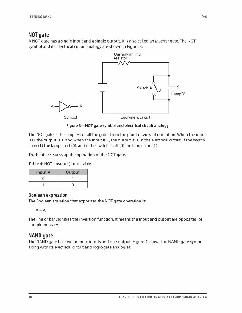
NOT gateA NOT gate has a single input and a single output. It is also called an inverter gate. The NOT symbol and its electrical circuit analogy are shown in Figure 3.
01
A
Symbol Equivalent circuit
Switch ALamp Y
A
Current-limitingresistor
Figure 3—NOT gate symbol and electrical circuit analogy
The NOT gate is the simplest of all the gates from the point of view of operation. When the input is 0, the output is 1, and when the input is 1, the output is 0. In the electrical circuit, if the switch is on (1) the lamp is off (0), and if the switch is off (0) the lamp is on (1).
Truth table 4 sums up the operation of the NOT gate.
Table 4: NOT (Inverter) truth table
Input A Output0 11 0
Boolean expressionThe Boolean equation that expresses the NOT gate operation is:
A = A
The line or bar signifies the inversion function. It means the input and output are opposites, or complementary.
NAND gateThe NAND gate has two or more inputs and one output. Figure 4 shows the NAND gate symbol, along with its electrical circuit and logic-gate analogies.

LEARNING TASk 2 D-6
CONSTRUCTION ELECTRICIAN APPRENTICESHIP PROGRAM: LEVEL 4 31
Symbol Electrical equivalent
Lamp YAB
Y
0 1
Switch BA • BA
BY = A • B
Current-limitingresistor
Gate equivalent
Switch A
0 1
Figure 4—NAND gate symbol with electrical circuit and logic-gate analogies
The NAND gate symbol is an AND gate symbol with a bubble, or inversion, on the output. The bubble is equivalent to putting an inverter at the output of an AND gate. For the same inputs, the outputs of the AND and NAND gates are opposites, or complementary.
The operation of the NAND gate is analogous to an electrical circuit with the switches and lamp connected as shown. The NAND gate operation is said to be an inversion of the AND gate operation; and the NAND and AND gates are described as complementary. The lamp will not light when switch A and switch B are closed. If either one is open, or if both are open, the lamp will light. Truth table 5 sums up the operation of the NAND gate.
Table 5: NAND truth table
Input A Input B Output Y0 0 11 0 10 1 11 1 0
Boolean expressionThe Boolean equation that expresses the NAND gate operation is:
A • B = C or AB = C
The • sign here stands for AND, as before. The solid line over both inputs is crucial. It says that only when the inputs A and B are high, the output will be low.
The behaviour of any NAND gate may be expressed by the statement Any low gives a high. This means that if there is any input 0, the output will be 1.

LEARNING TASk 2 D-6
32 CONSTRUCTION ELECTRICIAN APPRENTICESHIP PROGRAM: LEVEL 4
NOR gateThe NOR gate has two or more inputs and one output. Figure 5 shows the symbol for the NOR gate, along with its electrical circuit and logic gate equivalents.
0 1
Symbol Equivalent circuit
Lamp YSwitch B
A + BAB
Y = A + B
Current-limitingresistor
Switch A
0 1
AB
Y
Gate equivalent
Figure 5—NOR gate symbol with electrical circuit and logic-gate analogies
The NOR gate symbol is an OR gate symbol with a bubble, or “inversion”, on the output. The bubble is equivalent to putting an inverter at the output of an OR gate. For the same inputs, the outputs of the OR and NOR gates are opposites. This is similar to the contrast between AND and NAND gates. The operation of the NOR gate is analogous to an electrical circuit with the switches and lamp connected as shown in Figure 5. The NOR gate operation is an inversion of the OR gate operation. The lamp will not light if switch A or switch B is closed, or if both are closed. The lamp will light only when A and B are both open. The NOR gate operation is similar. Any 1 input will make an output 0. It follows that if both inputs are 1 the output is 0 also. Only when there is no 1 input (both inputs are 0) will the output be 1. Truth table 6 sums up the operation of the NOR gate.
Table 6: NOR truth table
Input A Input B Output Y
0 0 1
1 0 0
0 1 0
1 1 0
The NOR and OR gates are said to be complementary. Notice that for the same sets of inputs the outputs of OR and NOR gates are opposite or complementary.
Boolean expressionThe Boolean equation that expresses the NOR gate operation is:
A + B = Y
The + sign here stands for OR, as in the previous example. The solid line over both inputs is crucial. It means when inputs A or B are high, the output is low.
LEARNING TASk 2 D-6
CONSTRUCTION ELECTRICIAN APPRENTICESHIP PROGRAM: LEVEL 4 33
The behaviour of any NOR gate may be expressed by the statement: Any high gives a low. This means that if there is any input 1, the output will be 0.
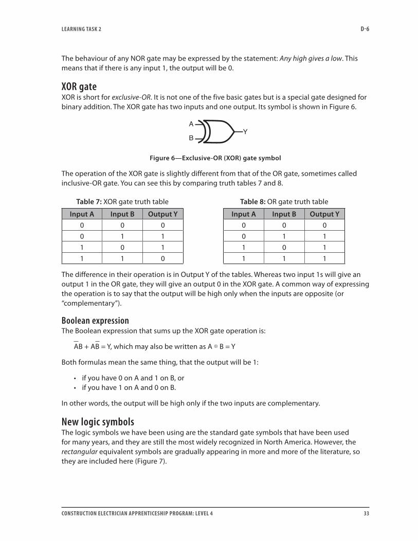
XOR gateXOR is short for exclusive-OR. It is not one of the five basic gates but is a special gate designed for binary addition. The XOR gate has two inputs and one output. Its symbol is shown in Figure 6.
A
BY
Figure 6—Exclusive-OR (XOR) gate symbol
The operation of the XOR gate is slightly different from that of the OR gate, sometimes called inclusive-OR gate. You can see this by comparing truth tables 7 and 8.
Table 7: XOR gate truth table Table 8: OR gate truth table
Input A Input B Output Y Input A Input B Output Y0 0 0 0 0 00 1 1 0 1 11 0 1 1 0 11 1 0 1 1 1
The difference in their operation is in Output Y of the tables. Whereas two input 1s will give an output 1 in the OR gate, they will give an output 0 in the XOR gate. A common way of expressing the operation is to say that the output will be high only when the inputs are opposite (or “complementary”).
Boolean expressionThe Boolean expression that sums up the XOR gate operation is:
AB + AB = Y, which may also be written as A ⊕ B = Y
Both formulas mean the same thing, that the output will be 1:
• if you have 0 on A and 1 on B, or • if you have 1 on A and 0 on B.
In other words, the output will be high only if the two inputs are complementary.
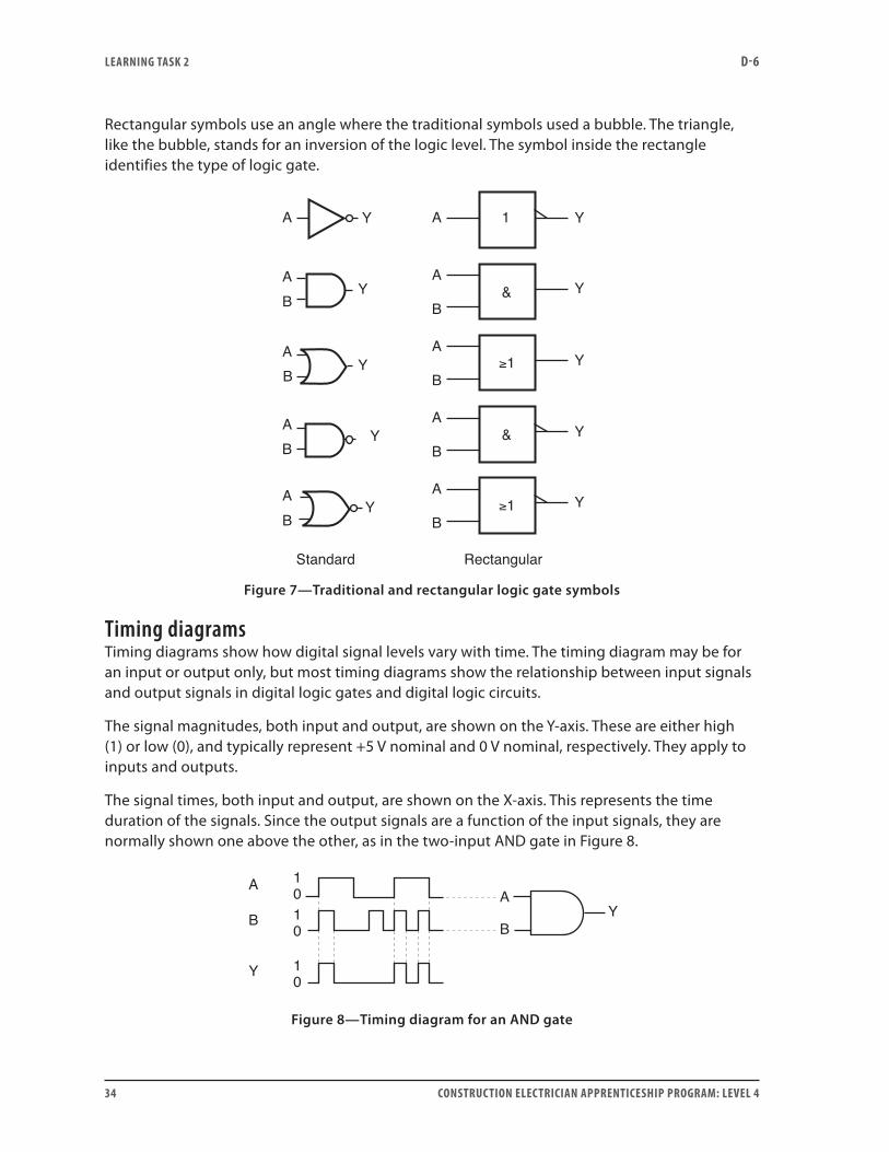
New logic symbolsThe logic symbols we have been using are the standard gate symbols that have been used for many years, and they are still the most widely recognized in North America. However, the rectangular equivalent symbols are gradually appearing in more and more of the literature, so they are included here (Figure 7).
LEARNING TASk 2 D-6
34 CONSTRUCTION ELECTRICIAN APPRENTICESHIP PROGRAM: LEVEL 4
Rectangular symbols use an angle where the traditional symbols used a bubble. The triangle, like the bubble, stands for an inversion of the logic level. The symbol inside the rectangle identifies the type of logic gate.
AB
Y
AB
Y
A
AB
Y
AB
Y
Y A
A
B
A
B
A
B
A
B
Y
Y
Y
Y
Y
1
&
≥1
&
≥1
Standard Rectangular
Figure 7—Traditional and rectangular logic gate symbols
Timing diagramsTiming diagrams show how digital signal levels vary with time. The timing diagram may be for an input or output only, but most timing diagrams show the relationship between input signals and output signals in digital logic gates and digital logic circuits.
The signal magnitudes, both input and output, are shown on the Y-axis. These are either high (1) or low (0), and typically represent +5 V nominal and 0 V nominal, respectively. They apply to inputs and outputs.
The signal times, both input and output, are shown on the X-axis. This represents the time duration of the signals. Since the output signals are a function of the input signals, they are normally shown one above the other, as in the two-input AND gate in Figure 8.
1010
10
A
B
Y
A
BY
Figure 8—Timing diagram for an AND gate
LEARNING TASk 2 D-6
CONSTRUCTION ELECTRICIAN APPRENTICESHIP PROGRAM: LEVEL 4 35
The output of an AND gate is high only when all inputs are high. In other words, if any input is low, the output will be low. Thus, for the set of input signals A and B in Figure 8, the output will be as shown.
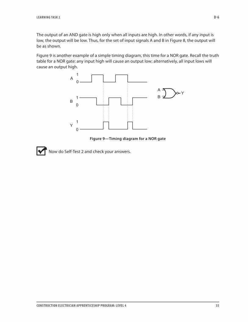
Figure 9 is another example of a simple timing diagram, this time for a NOR gate. Recall the truth table for a NOR gate: any input high will cause an output low; alternatively, all input lows will cause an output high.
Figure 9—Timing diagram for a NOR gate
Now do Self-Test 2 and check your answers.

LEARNING TASk 2 D-6
36 CONSTRUCTION ELECTRICIAN APPRENTICESHIP PROGRAM: LEVEL 4
Self-Test 2
1. Draw the standard symbols for the five basic logic gates.
2. Another name for a NOT gate is a(n) gate.
3. In a two-input AND gate, a 1 and a 0 applied to the inputs will produce a
output.
4. What input signals must you have in order that the output of a NAND gate is low?
5. In a NOR gate any input gives an output low.
6. Write the Boolean equation for a three-input (A, B, C) OR gate. Let the output be Y.
7. A NAND gate acts like a combination of what two other gates?
8. Signals 1 and 0 applied to inputs A and B respectively of a NOR gate will result in a
output.
9. An AND gate behaves like a conventional electric circuit that has switches in:
a. series
b. parallel

LEARNING TASk 2 D-6
CONSTRUCTION ELECTRICIAN APPRENTICESHIP PROGRAM: LEVEL 4 37
10. An OR gate behaves like a conventional electric circuit that has switches in:
a. series
b. parallel
11. In an XOR gate the output will be 1 only when the two inputs are:
a. 1
b. 0
c. same
d. complementary
12. Write the Boolean expression for an XOR gate having inputs A and B and output Y.
13. Draw the rectangular symbols for:
a. a two-input AND logic gate
b. a two-input OR logic gate
LEARNING TASk 2 D-6
38 CONSTRUCTION ELECTRICIAN APPRENTICESHIP PROGRAM: LEVEL 4
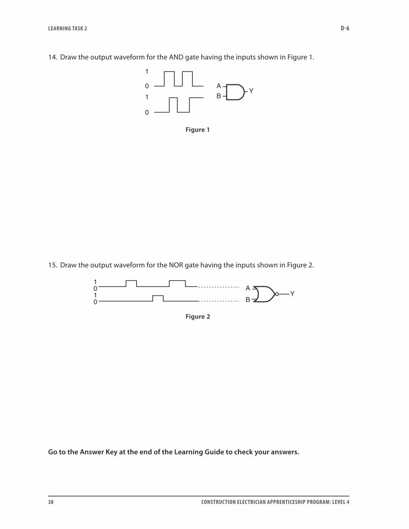
14. Draw the output waveform for the AND gate having the inputs shown in Figure 1.
AB
Y
1
01
0
Figure 1
15. Draw the output waveform for the NOR gate having the inputs shown in Figure 2.
AB
1010
Y
Figure 2
Go to the Answer Key at the end of the Learning Guide to check your answers.
CONSTRUCTION ELECTRICIAN APPRENTICESHIP PROGRAM: LEVEL 4 39
Learning Task 3:
Describe boolean algebraBoolean algebra is named after George Boole, a 19th-century mathematician and logician. His work was related to the thought processes and the representation of logical argument by logical algebra. It was not until about 100 years later, however, that his algebra was applied to mechanical and electrical devices.
Boolean algebra is a tool to mathematically design, simplify and implement logic circuits. For example, to get a drink from a dispensing machine you can usually pay with a variety of coins. Your drink selection may also include choices of cream and sugar, and so on. To design the circuit board of the dispensing machine, designers can use Boolean expressions to represent the logic-gate circuits.
A logic gate is also a two-state variable: inputs and outputs are either high (1) or low (0). In 1938, a professor at the Massachusetts Institute of Technology (MIT) described how Boolean algebra could be used to represent switching circuits that have two distinct states. For example, YES or NO, OFF or ON, NIGHT or DAY, and so on.
Boolean algebra and logic-gate circuitsIf we recall the 2-input AND gate, and use A and B to represent the digital inputs and Y the digital output, the Boolean expression or statement that describes it is A • B = Y. Likewise, a 3-input OR gate having inputs A, B and C, and output Y would have the Boolean expression A + B + C = Y. These expressions are written and spoken as follows:
• Written as: A • B = Y spoken as: A and B equals Y• Written as: A + B = Y spoken as: A or B equals Y
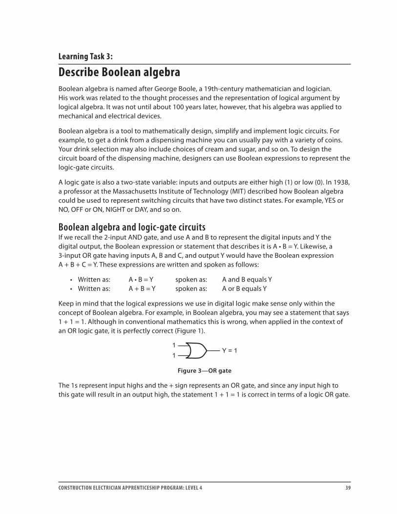
Keep in mind that the logical expressions we use in digital logic make sense only within the concept of Boolean algebra. For example, in Boolean algebra, you may see a statement that says 1 + 1 = 1. Although in conventional mathematics this is wrong, when applied in the context of an OR logic gate, it is perfectly correct (Figure 1).
Figure 3—OR gate
The 1s represent input highs and the + sign represents an OR gate, and since any input high to this gate will result in an output high, the statement 1 + 1 = 1 is correct in terms of a logic OR gate.
LEARNING TASk 3 D-6
40 CONSTRUCTION ELECTRICIAN APPRENTICESHIP PROGRAM: LEVEL 4
Likewise, another Boolean expression says A + (A • B) = A. Although at first it appears to contradict itself, this expression makes sense in terms of the logic gate in Figure 2.
Figure 4—Logic-gate circuit
The output Y in Figure 2 depends on A only. If A =1, the output at Y will be 1 regardless of whether B is 1 or 0. Likewise, if A = 0, the output at Y will be 0, again regardless of whether B is 0 or 1.
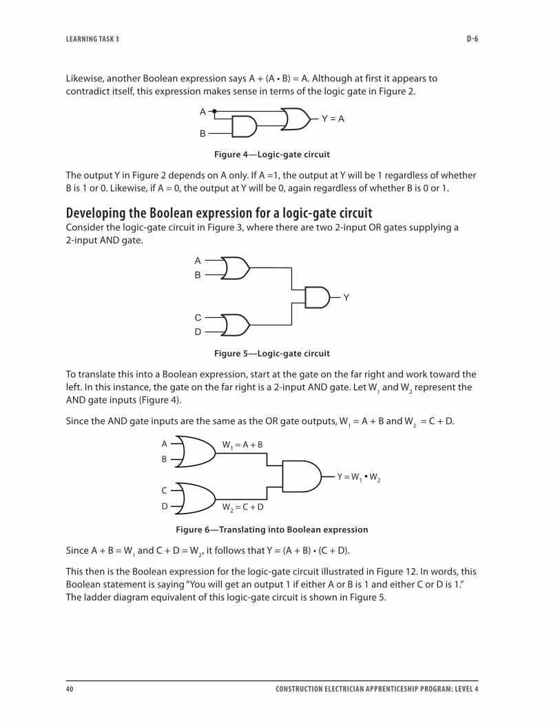
Developing the Boolean expression for a logic-gate circuitConsider the logic-gate circuit in Figure 3, where there are two 2-input OR gates supplying a 2-input AND gate.
Figure 5—Logic-gate circuit
To translate this into a Boolean expression, start at the gate on the far right and work toward the left. In this instance, the gate on the far right is a 2-input AND gate. Let W1 and W2 represent the AND gate inputs (Figure 4).
Since the AND gate inputs are the same as the OR gate outputs, W1 = A + B and W2 = C + D.
A
B
C
D
W1 = A + B
W2 = C + D
Y = W1 • W2
Figure 6—Translating into Boolean expression
Since A + B = W1 and C + D = W2, it follows that Y = (A + B) • (C + D).
This then is the Boolean expression for the logic-gate circuit illustrated in Figure 12. In words, this Boolean statement is saying “You will get an output 1 if either A or B is 1 and either C or D is 1.” The ladder diagram equivalent of this logic-gate circuit is shown in Figure 5.

LEARNING TASk 3 D-6
CONSTRUCTION ELECTRICIAN APPRENTICESHIP PROGRAM: LEVEL 4 41
Figure 7—Ladder diagram equivalent
Developing a logic-gate circuit from a Boolean expressionTo build a logic-gate circuit from a Boolean expression, the process is reversed.
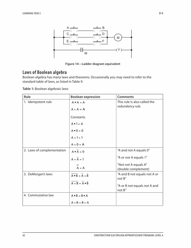
For the Boolean expression Y = (A • B) + (C • D) + (E • F), this process is as follows:
Step 1: Start by letting A • B = W1, C • D = W2, and E • F = W3.
Therefore, Y = W1 + W2 + W3. This represents a 3-input OR gate, as shown in Figure 6.
Figure 8—3-input OR logic gate
Step 2: Since W1 = A • B, W1 is the output of an AND gate having inputs A and B. Similarly, W2 is the output of an AND gate having inputs C and D, and W3 is the output of an AND gate having inputs E and F. The logic circuit diagram of this expression is shown in Figure 7.
Figure 9—Logic-gate circuit of Boolean expression
The ladder diagram equivalent of this circuit is shown in Figure 10.
LEARNING TASk 3 D-6
42 CONSTRUCTION ELECTRICIAN APPRENTICESHIP PROGRAM: LEVEL 4
Figure 10—Ladder diagram equivalent
Laws of Boolean algebraBoolean algebra has many laws and theorems. Occasionally you may need to refer to the standard table of laws, as listed in Table 9.
Table 1: Boolean algebraic laws
Rule Boolean expression Comments1. Idempotent rule A A A
A A A
• =
+ =
Constants
A A
A
A
A A
•
•
1
0 0
1 1
0
=
=
+ =
+ =
This rule is also called the redundancy rule.
2. Laws of complementation A A
A A
A A
• =
+ =
=
0
1
“A and not A equals 0”
“A or not A equals 1”
“Not not A equals A” (double complement)
3. DeMorgan’s laws A B A B
A B A B
•
•
= +
+ =
“A and B not equals not A or not B”
“A or B not equals not A and not B”
4. Commutative law A B B A
A B B A
• •=
+ = +

LEARNING TASk 3 D-6
CONSTRUCTION ELECTRICIAN APPRENTICESHIP PROGRAM: LEVEL 4 43
5. Distributive laws A B C A B A C
A B C A B A C
• ( ) ( • ) ( • )
( • ) ( ) • ( )
+ = +
+ = + +
6. Associative laws A B C C A B
A B C C A B
• ( • ) • ( • )
( ) ( )
=
+ + = + +
7. Laws of absorption A A B A
A A B A
• ( )
( • )
+ =
+ =
DeMorgan’s lawsDeMorgan’s laws (Table 1, Rule 3) show that logic-gate circuits can be constructed in different ways to achieve the same end result. In other words, this is equivalent to us saying “a glass is half empty” or “a glass is half full.” DeMorgan’s laws show us the duality of logic expressions and logic-gate circuits.
DeMorgan’s two laws state:
A B A B• = + spoken as: A and B not equals not A oor not B
spoken as: A or B not equalA B A B+ = • ss not A and not B
DeMorgan’s first lawConsider the first law, A B A B• = + . Since DeMorgan is saying that Y A B= • , and also that Y A B= + , then the truth table for each of these expressions must be the same (Figure 9). Examine the variable inputs (1) and (0) in the truth table. Notice that the outputs are the same for each gate, for any pair of inputs.
Figure 11—DeMorgan equivalents and truth table
The two ladder diagrams in Figure 12 are the equivalent of the two logic circuits in Figure 11.
LEARNING TASk 3 D-6
44 CONSTRUCTION ELECTRICIAN APPRENTICESHIP PROGRAM: LEVEL 4
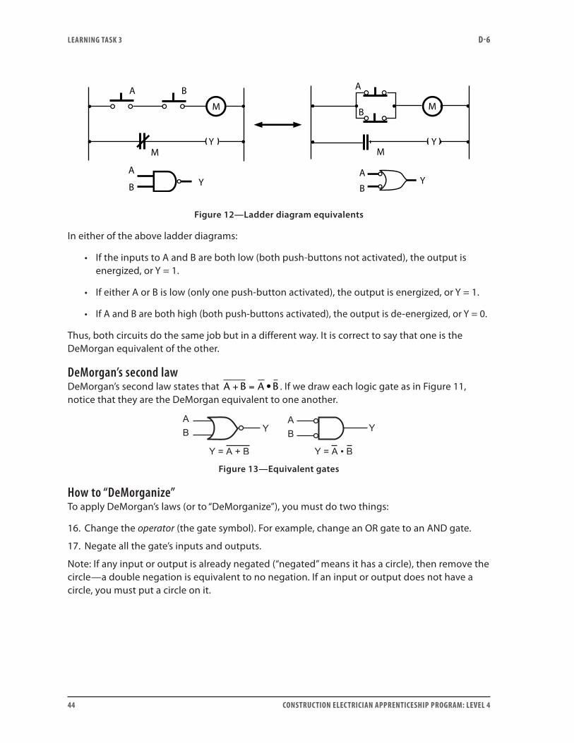
Figure 12—Ladder diagram equivalents
In either of the above ladder diagrams:
• If the inputs to A and B are both low (both push-buttons not activated), the output is energized, or Y = 1.
• If either A or B is low (only one push-button activated), the output is energized, or Y = 1.
• If A and B are both high (both push-buttons activated), the output is de-energized, or Y = 0.
Thus, both circuits do the same job but in a different way. It is correct to say that one is the DeMorgan equivalent of the other.
DeMorgan’s second lawDeMorgan’s second law states that A B A B+ = • . If we draw each logic gate as in Figure 11, notice that they are the DeMorgan equivalent to one another.
Figure 13—Equivalent gates
How to “DeMorganize”To apply DeMorgan’s laws (or to “DeMorganize”), you must do two things:
16. Change the operator (the gate symbol). For example, change an OR gate to an AND gate.
17. Negate all the gate’s inputs and outputs.
Note: If any input or output is already negated (“negated” means it has a circle), then remove the circle—a double negation is equivalent to no negation. If an input or output does not have a circle, you must put a circle on it.

LEARNING TASk 3 D-6
CONSTRUCTION ELECTRICIAN APPRENTICESHIP PROGRAM: LEVEL 4 45
Example 1: What is the DeMorgan equivalent of the AND logic gate in the figure below?
Solution:
1. Change the AND symbol into an OR symbol.
2. Negate all the inputs and outputs.
Example 2: Find the DeMorgan equivalent of the logic circuit below.
Solution:
1. Make the OR symbol an AND symbol.
2. Remove the circles from the inputs.
3. Put a circle on the output.
•

LEARNING TASk 3 D-6
46 CONSTRUCTION ELECTRICIAN APPRENTICESHIP PROGRAM: LEVEL 4
Example 3: Find the DeMorgan equivalent of the logic circuit below.
Solution:
1. Make the AND symbol an OR symbol.
2. Remove the circles from input A and the output.
3. Insert a circle on inputs B and C.
Implications of DeMorganizingOften a DeMorgan equivalent is easier to understand than the original logic gate. For example, look at the two equivalent gates in Figure 12.
Figure 14—Equivalent logic gates
Many people find it easier to work with the negated OR gate rather than with the NAND gate. It is easier to read Figure 12(b) as “Any input low gives an output high” rather than Figure 12(a), which reads “If all inputs are high you get an output low.”
Likewise, while a logic diagram may illustrate a negated OR gate, the actual circuit component itself could be a NAND gate.
Encoding and decodingComputers, calculators and programmable logic controllers cannot work directly with decimals, letters and symbols. Such data must be transmitted from the keyboard to the central processing unit (cpu) in some form of code. Some of the more common codes are Binary-Coded-Decimal (BCD) and ASCII, but there are several others.
In order to produce these codes when a keyboard character, number or symbol is pressed, some form of encoder is needed. The encoder changes the letters, numbers and symbols into “bits” of information that the computer’s CPU can read. These bits of information are actually voltage levels, which are either high (1) or low (0).
LEARNING TASk 3 D-6
CONSTRUCTION ELECTRICIAN APPRENTICESHIP PROGRAM: LEVEL 4 47
A decoder does the opposite of an encoder. It takes the coded information and translates it into the familiar everyday language of numbers, characters and symbols. These then appear on the screen or on the printed page.
Encoders and decoders are made up of groups of logic gates, and they may be individually packaged as integrated circuits (ICs) or may form part of other ICs that have additional integrated circuits.
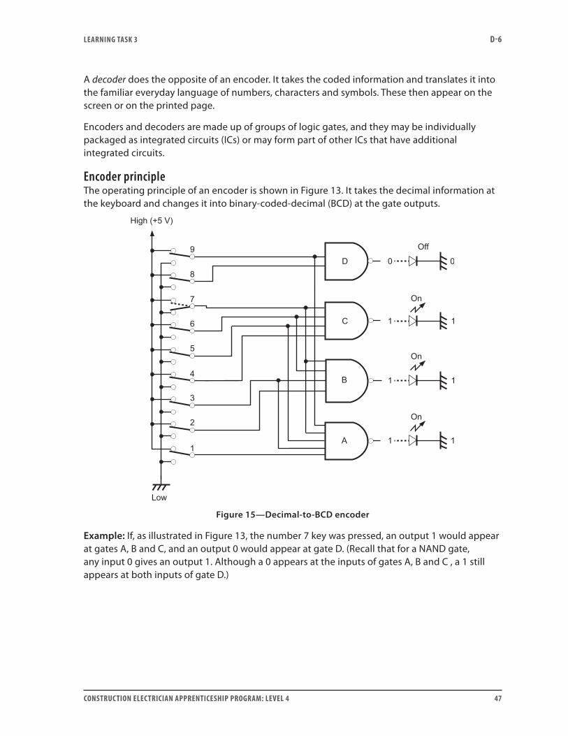
Encoder principleThe operating principle of an encoder is shown in Figure 13. It takes the decimal information at the keyboard and changes it into binary-coded-decimal (BCD) at the gate outputs.
Figure 15—Decimal-to-BCD encoder
Example: If, as illustrated in Figure 13, the number 7 key was pressed, an output 1 would appear at gates A, B and C, and an output 0 would appear at gate D. (Recall that for a NAND gate, any input 0 gives an output 1. Although a 0 appears at the inputs of gates A, B and C , a 1 still appears at both inputs of gate D.)
LEARNING TASk 3 D-6
48 CONSTRUCTION ELECTRICIAN APPRENTICESHIP PROGRAM: LEVEL 4
If the outputs were fed to light-emitting diodes (LEDs), as indicated by the broken lines, lights A, B and C would be ON and light D would be OFF. Thus the readout of the gates DCBA is 0111. Recall that 7 in BCD is 0111.
Now try any other keyboard number, follow the inputs to the gates, and verify that the resulting 1s and 0s appearing at the output of the gates correspond to the BCD equivalent of that number key.
The above example illustrates the principle of encoding. Encoding can be achieved using different logic gates and several circuit designs.
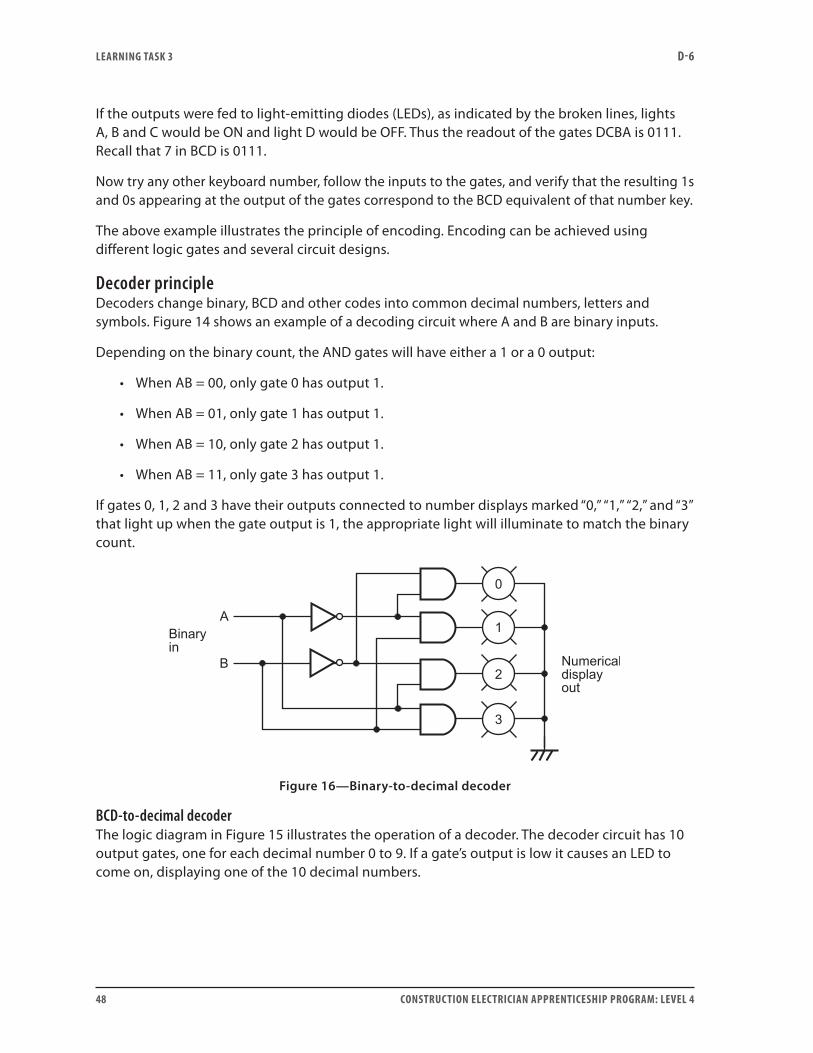
Decoder principleDecoders change binary, BCD and other codes into common decimal numbers, letters and symbols. Figure 14 shows an example of a decoding circuit where A and B are binary inputs.
Depending on the binary count, the AND gates will have either a 1 or a 0 output:
• When AB = 00, only gate 0 has output 1.
• When AB = 01, only gate 1 has output 1.
• When AB = 10, only gate 2 has output 1.
• When AB = 11, only gate 3 has output 1.
If gates 0, 1, 2 and 3 have their outputs connected to number displays marked “0,” “1,” “2,” and “3” that light up when the gate output is 1, the appropriate light will illuminate to match the binary count.
Figure 16—Binary-to-decimal decoder
BCD-to-decimal decoderThe logic diagram in Figure 15 illustrates the operation of a decoder. The decoder circuit has 10 output gates, one for each decimal number 0 to 9. If a gate’s output is low it causes an LED to come on, displaying one of the 10 decimal numbers.
LEARNING TASk 3 D-6
CONSTRUCTION ELECTRICIAN APPRENTICESHIP PROGRAM: LEVEL 4 49
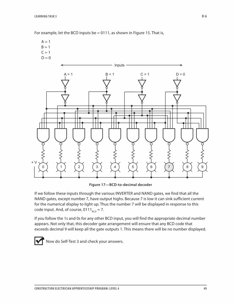
For example, let the BCD inputs be = 0111, as shown in Figure 15. That is,
A = 1 B = 1 C = 1 D = 0
Figure 17—BCD-to-decimal decoder
If we follow these inputs through the various INVERTER and NAND gates, we find that all the NAND gates, except number 7, have output highs. Because 7 is low it can sink sufficient current for the numerical display to light up. Thus the number 7 will be displayed in response to this code input. And, of course, 0111BCD = 7.
If you follow the 1s and 0s for any other BCD input, you will find the appropriate decimal number appears. Not only that, this decoder gate arrangement will ensure that any BCD code that exceeds decimal 9 will keep all the gate outputs 1. This means there will be no number displayed.
Now do Self-Test 3 and check your answers.
LEARNING TASk 3 D-6
50 CONSTRUCTION ELECTRICIAN APPRENTICESHIP PROGRAM: LEVEL 4
Self-Test 3
1. Boolean algebra assumes that variables have how many states?
2. Draw the logic-gate circuit of the Boolean expression Y = A • (B + C).
3. Draw the equivalent ladder diagram for the logic-gate circuit in Question 3.
4. Write the Boolean expressions for the logic-gate circuits in Figure 3(a) and (b).
Figure 1

LEARNING TASk 3 D-6
CONSTRUCTION ELECTRICIAN APPRENTICESHIP PROGRAM: LEVEL 4 51
5. Given Y = A + B + C:
a. Draw the gate circuit it represents.
b. Draw the DeMorgan equivalent circuit and write its Boolean expression.
6. What are the two operations that must be done to “DeMorganize” an expression?
7. Draw the DeMorgan equivalent of the logic-gate circuit in Figure 2, and write its Boolean expression.
Figure 2
8. How many different types of codes are used in computers, programmable logic controllers, etc.?
a. 2
b. 3
c. 4
d. greater than 4

LEARNING TASk 3 D-6
52 CONSTRUCTION ELECTRICIAN APPRENTICESHIP PROGRAM: LEVEL 4
9. If switch 5 is pressed in the decimal-to-BCD encoder in Figure 13, Learning Task 1, what is the status of outputs A, B, C and D?
10. In the BCD-to-decimal decoder in Figure 15, Learning Task 1, what are the logic inputs A, B, C, and D if LED 6 is ON?
11. In the BCD-to-decimal decoder in Figure 15, Learning Task 1, what will be the status of the LEDs if the inputs are A = 0, B = 0, C = 1 and D = 1?
Go to the Answer Key at the end of the Learning Guide to check your answers.
CONSTRUCTION ELECTRICIAN APPRENTICESHIP PROGRAM: LEVEL 4 53
Learning Task 4:
Describe the operation of special combination logic circuitsThe logic circuits considered thus far have been combination circuits whose output levels at any instant depend on the input levels at that time. Any prior input conditions have no effect on the present outputs because combination logic circuits have no memory.
Most digital systems, however, are made up of both combination circuits and memory elements. The most important memory element is the flip-flop, which is made up of an assembly of logic gates. Even though a logic gate, by itself, has no storage capability, gates can be connected together in ways that permit information to be stored.
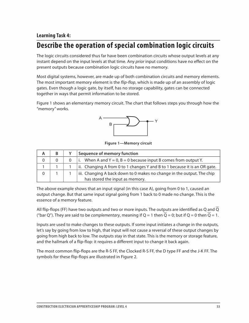
Figure 1 shows an elementary memory circuit. The chart that follows steps you through how the “memory” works.
Figure 1—Memory circuit
A B Y Sequence of memory function0 0 0 i. When A and Y = 0, B = 0 because input B comes from output Y. 1 1 1 ii. Changing A from 0 to 1 changes Y and B to 1 because it is an OR gate.0 1 1 iii. Changing A back down to 0 makes no change in the output. The chip
has stored the input as memory.
The above example shows that an input signal (in this case A), going from 0 to 1, caused an output change. But that same input signal going from 1 back to 0 made no change. This is the essence of a memory feature.
All flip-flops (FF) have two outputs and two or more inputs. The outputs are identified as Q and Q (“bar Q”). They are said to be complementary, meaning if Q = 1 then Q = 0; but if Q = 0 then Q = 1.
Inputs are used to make changes to these outputs. If some input initiates a change in the outputs, let’s say by going from low to high, that input will not cause a reversal of these output changes by going from high back to low. The outputs stay in that state. This is the memory or storage feature, and the hallmark of a flip-flop: it requires a different input to change it back again.
The most common flip-flops are the R-S FF, the Clocked R-S FF, the D type FF and the J-K FF. The symbols for these flip-flops are illustrated in Figure 2.

LEARNING TASk 4 D-6
54 CONSTRUCTION ELECTRICIAN APPRENTICESHIP PROGRAM: LEVEL 4
Figure 2—Flip-flop symbols
R-S flip-flop (R-S latch)The R-S FF is the simplest of all the flip-flops and is often referred to as an R-S latch. It can be made up of cross-connected NAND or NOR gates.
• R and S stand for reset and set.
• Cross-connected means an output is fed back to an input.
We will take a detailed look at its operation, because if you can follow this operation you will get a sound appreciation of flip-flop operation in general.
To follow the operation of this circuit, it is important to keep in mind the following:
• For a NOR gate, any input 1 gives an output 0.
• The function of S is to set Q to 1 (and by implication make Q = 0).
• The function of R is to reset Q to 0 (and by implication make Q = 1).
• The NOR gate FF is said to be active high: an input signal going from low to high (0 to 1) can initiate an output change; but going from high to low (1 to 0) cannot initiate an output change.
Example 1: Referring to the NOR FF in Figure 3, let’s set S = 1 and R = 0. This makes Q = 1 and Q = 0.
Figure 3—R-S flip-flop using NOR gates

CONSTRUCTION ELECTRICIAN APPRENTICESHIP PROGRAM: LEVEL 4 55
Why is Q = 1?
• Letting S = 1 makes gate 1 output low.
• The cross-connection from output of gate 1 back to input of gate 2 makes the second input at gate 2 low (the same as Q).
• Gate 2 now has two low inputs, making its output high.
• The cross-connection from gate 2 makes the second input at gate 1 high.
• Gate 1 now has two high inputs.
Since one high input is sufficient to keep Q = 0, input S can go to 0 without changing the output.
Thus, making S = 1 sets (or latches) the outputs to a given state. Making S = 0 does not reset, or unlatch, them. (This will be the function of R.) So when S is returned to 0 (and S = R = 0), the flip-flop is said to be in the memory mode.
Example 2: Now let’s set S = 0 and R = 1. This makes Q = 0 and Q = 1, the exact opposite of Example 1.
Why is Q = 0?
• Letting R = 1 makes gate 2 output low.
• Because of the cross-connection, gate 2 low makes the second input to gate 1 low.
• Gate 1 now has two low inputs, making its output high.
• The cross-connection from gate 1 makes the second input to gate 2 high.
• Gate 2 now has two high inputs.
Since one high input is sufficient to keep Q = 0, input R can go to 0 without changing the outputs. As before, when S = R = 0, the flip-flop is back in memory mode.
Examples 1 and 2 show how the function of S is to set Q = 1 and the function of R is to reset Q = 0.
Example 3: What if S = R = 1?
• Both Q and Q would go low.
This is called an illegal, or prohibited, condition.
Avoid the prohibited condition. By definition, the outputs of a flip-flop are complementary.

LEARNING TASk 4 D-6
56 CONSTRUCTION ELECTRICIAN APPRENTICESHIP PROGRAM: LEVEL 4
Truth table for R-S flip-flopThe truth table in Figure 4 sums up the operation of the R-S FF. Note that the outputs in the memory state may be Q = 1 and Q = 0, or vice versa. It will depend on what the inputs were just before S = R = 0. (If they had been in the set state, the outputs would be those of the set state. If they had been in the reset state, the outputs would be those of the reset state.) Prove this yourself by running through the circuit in Figure 3.
Figure 4—Truth table for an R-S NOR gate flip-flop
NAND gate R-S FFAn R-S flip-flop can also be made with NAND gates. The NAND gate circuit with its DeMorgan equivalent is shown in Figure 5.
R S Q Q1 1 Memory/no charge1 0 1 0 Set0 1 0 1 Reset0 0 1 1 Prohibited
Figure 5—NAND gate R-S flip-flop
LEARNING TASk 4 D-6
CONSTRUCTION ELECTRICIAN APPRENTICESHIP PROGRAM: LEVEL 4 57
The operation of the NAND flip-flop (Figure 5[c]) is the exact opposite of the NOR gate:
• For a NAND gate, any input 0 gives an output 1.
• The function of S is to set Q to 1 (and by implication make Q = 0).
• The function of R is to reset Q to 0 (and by implication make Q = 1).
• The NAND gate FF is said to be active low. This means that an input signal from high to low (1 to 0) can initiate an output change; but going from low to high (0 to 1) cannot initiate an output change. In other words, the memory state is activated when S = R = 1.
What if S = R = 0?
• Both Q and Q would go high. This is a prohibited condition.
Avoid the prohibited condition. By definition the outputs of a flip-flop are complementary.
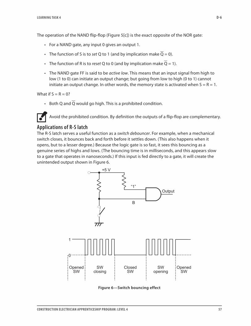
Applications of R-S latchThe R-S latch serves a useful function as a switch debouncer. For example, when a mechanical switch closes, it bounces back and forth before it settles down. (This also happens when it opens, but to a lesser degree.) Because the logic gate is so fast, it sees this bouncing as a genuine series of highs and lows. (The bouncing time is in milliseconds, and this appears slow to a gate that operates in nanoseconds.) If this input is fed directly to a gate, it will create the unintended output shown in Figure 6.
Figure 6—Switch bouncing effect
LEARNING TASk 4 D-6
58 CONSTRUCTION ELECTRICIAN APPRENTICESHIP PROGRAM: LEVEL 4
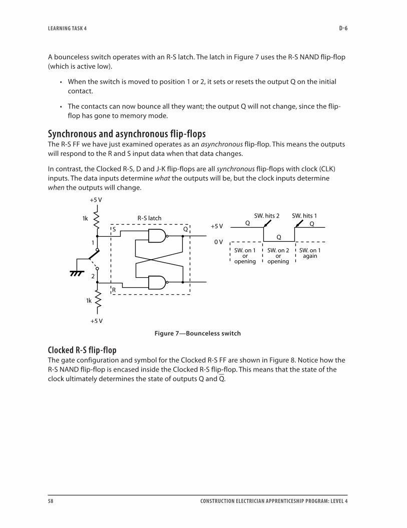
A bounceless switch operates with an R-S latch. The latch in Figure 7 uses the R-S NAND flip-flop (which is active low).
• When the switch is moved to position 1 or 2, it sets or resets the output Q on the initial contact.
• The contacts can now bounce all they want; the output Q will not change, since the flip-flop has gone to memory mode.
Synchronous and asynchronous flip-flopsThe R-S FF we have just examined operates as an asynchronous flip-flop. This means the outputs will respond to the R and S input data when that data changes.
In contrast, the Clocked R-S, D and J-K flip-flops are all synchronous flip-flops with clock (CLK) inputs. The data inputs determine what the outputs will be, but the clock inputs determine when the outputs will change.
0
Figure 7—Bounceless switch
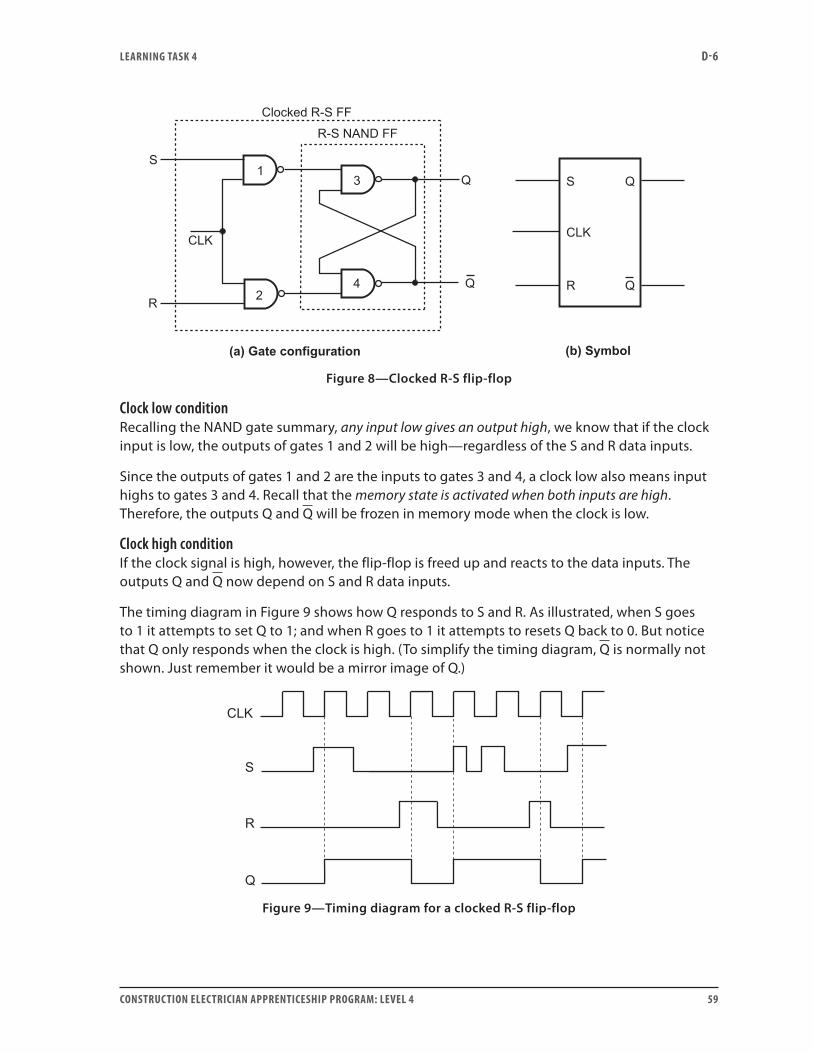
Clocked R-S flip-flopThe gate configuration and symbol for the Clocked R-S FF are shown in Figure 8. Notice how the R-S NAND flip-flop is encased inside the Clocked R-S flip-flop. This means that the state of the clock ultimately determines the state of outputs Q and Q.
LEARNING TASk 4 D-6
CONSTRUCTION ELECTRICIAN APPRENTICESHIP PROGRAM: LEVEL 4 59
Figure 8—Clocked R-S flip-flop
Clock low conditionRecalling the NAND gate summary, any input low gives an output high, we know that if the clock input is low, the outputs of gates 1 and 2 will be high—regardless of the S and R data inputs.
Since the outputs of gates 1 and 2 are the inputs to gates 3 and 4, a clock low also means input highs to gates 3 and 4. Recall that the memory state is activated when both inputs are high. Therefore, the outputs Q and Q will be frozen in memory mode when the clock is low.
Clock high conditionIf the clock signal is high, however, the flip-flop is freed up and reacts to the data inputs. The outputs Q and Q now depend on S and R data inputs.
The timing diagram in Figure 9 shows how Q responds to S and R. As illustrated, when S goes to 1 it attempts to set Q to 1; and when R goes to 1 it attempts to resets Q back to 0. But notice that Q only responds when the clock is high. (To simplify the timing diagram, Q is normally not shown. Just remember it would be a mirror image of Q.)
Figure 9—Timing diagram for a clocked R-S flip-flop

LEARNING TASk 4 D-6
60 CONSTRUCTION ELECTRICIAN APPRENTICESHIP PROGRAM: LEVEL 4
The truth table in Figure 10 sums up the operation of the Clocked R-S NAND flip-flop.
• When the clock = 0 there can be no changes—the outputs are frozen.
• When the clock = 1 the flip-flop is freed up. It can now react to the data inputs.
• Like the R-S FF, the Clocked R-S FF also has an illegal state; that is, when R and S = 1. Avoid this input combination.
Figure 10—Truth table for Clocked R-S flip-flop
D (data) type flip-flopThe logic symbol and truth table for the D type flip-flop are shown in Figure 11. The characteristic of D type flip-flops is that the outputs change when the clock input goes from low to high (on the rising, leading or positive edge). This is called a leading-edge triggered flip-flop, and it is indicated by the “>” symbol on the clock input.
(a) Symbol (b) Truth table
Figure 11—Leading-edge triggered D type flip-flop

LEARNING TASk 4 D-6
CONSTRUCTION ELECTRICIAN APPRENTICESHIP PROGRAM: LEVEL 4 61
The statement Q follows D on the arrival of the clock pulse sums up the operation of this flip-flop. The symbols ↑ and ↓ in the truth table illustrate the rising and falling clock inputs.
• If D = 0 and Q = 1, Q will change to 0 when the clock input changes from 0 to 1.
• If D = 1 and Q = 0, Q will change to 1 when the clock input changes from 0 to 1.
• If D = 0 and Q = 0, Q will remain unchanged when the clock input changes from 0 to 1.
• If D = 1 and Q = 1, Q will remain unchanged when the clock input changes from 0 to 1.
The timing diagram of a D type flip-flop is shown in Figure 12.
Figure 12—Timing diagram for a D type flip-flop
J-K flip-flopThe J-K flip-flop is the most widely used of the flip-flops because it possesses a unique toggle feature; and it can also be adapted to any of the other three flip-flops. The logic symbol and truth table are shown in Figure 13.
The clock input for a J-K flip-flop is edge triggered just like the D type. Many J-K types, however, use trailing-edge triggering, symbolized by the “o>” on the clock input (Figure 13[a]). The trailing edge is also called the falling or negative-going edge.
Figure 13—Trailing-edge triggered J-K flip-flop
LEARNING TASk 4 D-6
62 CONSTRUCTION ELECTRICIAN APPRENTICESHIP PROGRAM: LEVEL 4
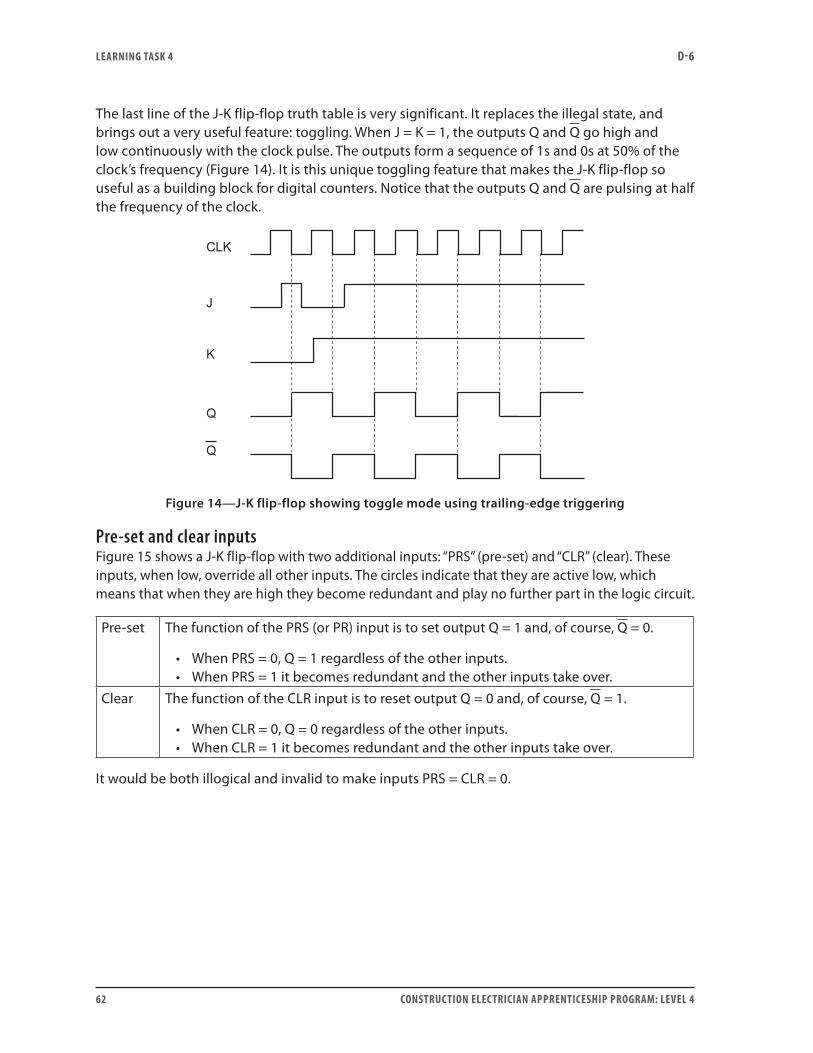
The last line of the J-K flip-flop truth table is very significant. It replaces the illegal state, and brings out a very useful feature: toggling. When J = K = 1, the outputs Q and Q go high and low continuously with the clock pulse. The outputs form a sequence of 1s and 0s at 50% of the clock’s frequency (Figure 14). It is this unique toggling feature that makes the J-K flip-flop so useful as a building block for digital counters. Notice that the outputs Q and Q are pulsing at half the frequency of the clock.
Figure 14—J-K flip-flop showing toggle mode using trailing-edge triggering
Pre-set and clear inputsFigure 15 shows a J-K flip-flop with two additional inputs: “PRS” (pre-set) and “CLR” (clear). These inputs, when low, override all other inputs. The circles indicate that they are active low, which means that when they are high they become redundant and play no further part in the logic circuit.
Pre-set The function of the PRS (or PR) input is to set output Q = 1 and, of course, Q = 0.
• When PRS = 0, Q = 1 regardless of the other inputs.• When PRS = 1 it becomes redundant and the other inputs take over.
Clear The function of the CLR input is to reset output Q = 0 and, of course, Q = 1.
• When CLR = 0, Q = 0 regardless of the other inputs.• When CLR = 1 it becomes redundant and the other inputs take over.
It would be both illogical and invalid to make inputs PRS = CLR = 0.

LEARNING TASk 4 D-6
CONSTRUCTION ELECTRICIAN APPRENTICESHIP PROGRAM: LEVEL 4 63
Figure 15—Clear and pre-set inputs on J-K flip-flop
PRS and CLR are used to put the flip-flop into an initial state, either Q = 1 or Q = 0. These inputs are available in nearly all commercial flip-flops and give the user a means of determining the initial output logic level of the flip-flop. This control is essential for counters and shift registers, which are explained later.
MultivibratorsIn digital circuits, the circuit action normally depends on having a noise-free rectangular-shaped wave with an edge that rises and/or falls sharply. A multivibrator is an oscillator or pulse generator that produces both square and rectangular waveforms. Multivibrators are usually ICs in the form of DIP packages with external components such as resistors and capacitors connected to them. They can also be assembled from discrete components.
Multivibrators are often classified according to their stability. The three classes are: astable, monostable and bistable.
Astable multivibratorsThe astable multivibrator is a logic circuit that oscillates back and forth between high and low states. It does not require an input signal, and it puts out a continuous train of digital pulses. This type of multivibrator is also called free-running. The astable multivibrator is often used to generate non-square waves.
There are several different devices that can produce this type of output, including the operational amplifier, the crystal oscillator and the 555 timer.
Monostable multivibratorUnlike the free-running astable multivibrator, the monostable multivibrator requires an input signal in order to change states. The monostable multivibrator is also known as a one-shot multivibrator or simply one shot, because one trigger pulse will cause the output to change state for a definite period of time.
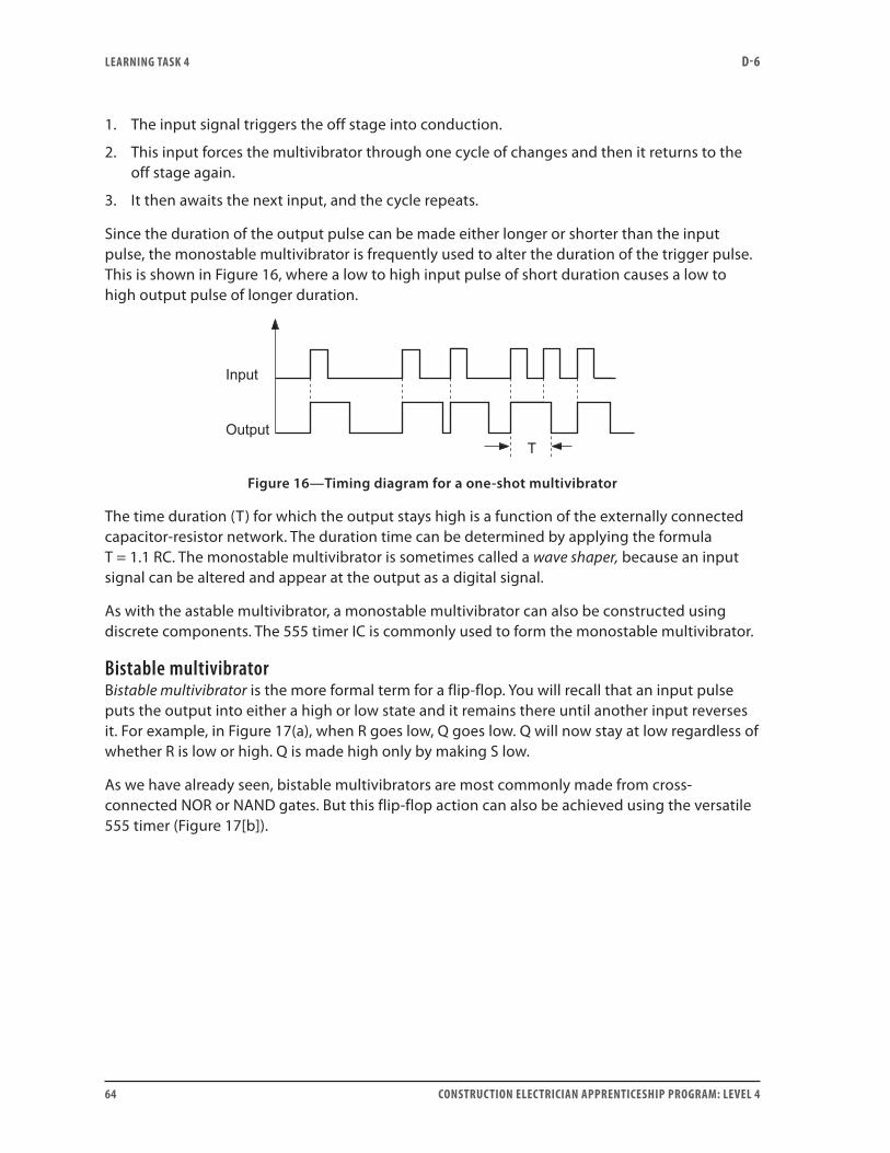
LEARNING TASk 4 D-6
64 CONSTRUCTION ELECTRICIAN APPRENTICESHIP PROGRAM: LEVEL 4
1. The input signal triggers the off stage into conduction.
2. This input forces the multivibrator through one cycle of changes and then it returns to the off stage again.
3. It then awaits the next input, and the cycle repeats.
Since the duration of the output pulse can be made either longer or shorter than the input pulse, the monostable multivibrator is frequently used to alter the duration of the trigger pulse. This is shown in Figure 16, where a low to high input pulse of short duration causes a low to high output pulse of longer duration.
Figure 16—Timing diagram for a one-shot multivibrator
The time duration (T) for which the output stays high is a function of the externally connected capacitor-resistor network. The duration time can be determined by applying the formula T = 1.1 RC. The monostable multivibrator is sometimes called a wave shaper, because an input signal can be altered and appear at the output as a digital signal.
As with the astable multivibrator, a monostable multivibrator can also be constructed using discrete components. The 555 timer IC is commonly used to form the monostable multivibrator.
Bistable multivibratorBistable multivibrator is the more formal term for a flip-flop. You will recall that an input pulse puts the output into either a high or low state and it remains there until another input reverses it. For example, in Figure 17(a), when R goes low, Q goes low. Q will now stay at low regardless of whether R is low or high. Q is made high only by making S low.
As we have already seen, bistable multivibrators are most commonly made from cross-connected NOR or NAND gates. But this flip-flop action can also be achieved using the versatile 555 timer (Figure 17[b]).
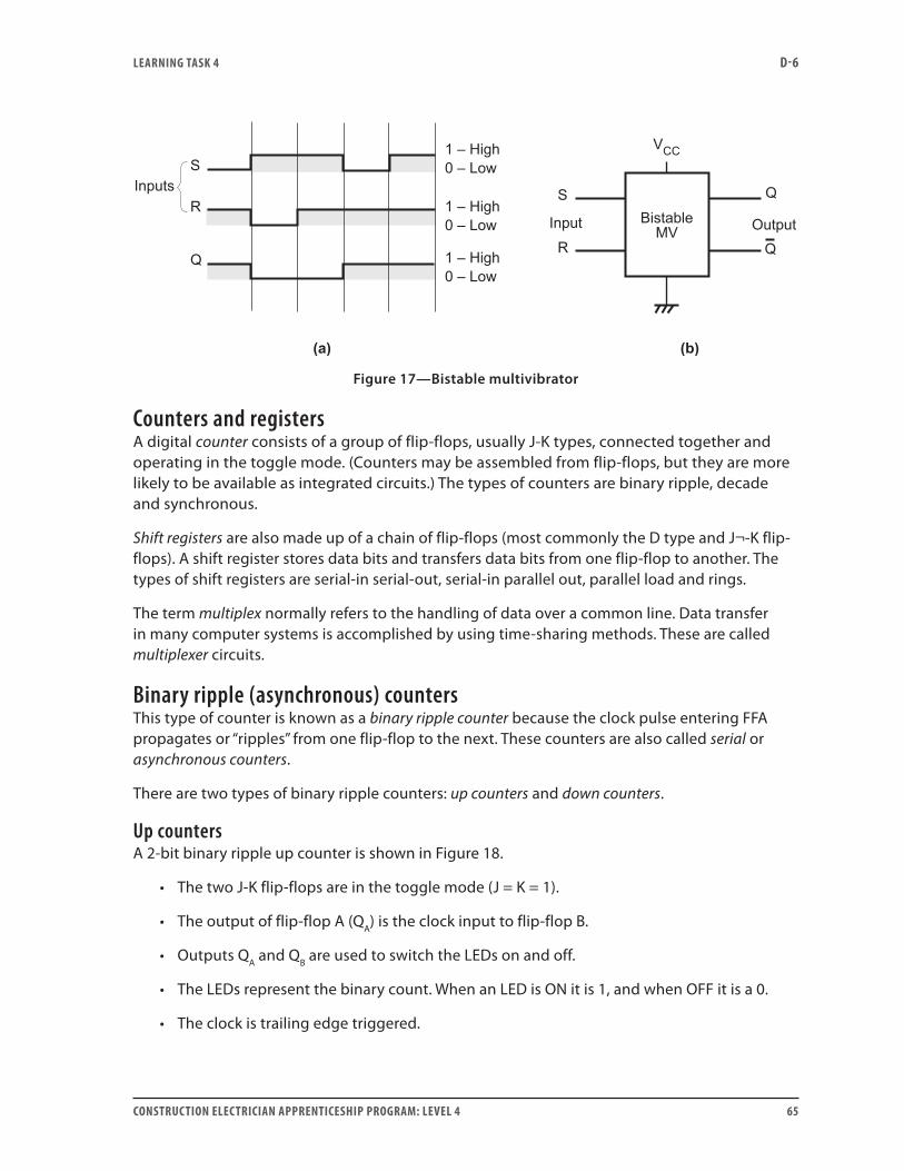
LEARNING TASk 4 D-6
CONSTRUCTION ELECTRICIAN APPRENTICESHIP PROGRAM: LEVEL 4 65
Figure 17—Bistable multivibrator
Counters and registersA digital counter consists of a group of flip-flops, usually J-K types, connected together and operating in the toggle mode. (Counters may be assembled from flip-flops, but they are more likely to be available as integrated circuits.) The types of counters are binary ripple, decade and synchronous.
Shift registers are also made up of a chain of flip-flops (most commonly the D type and J¬-K flip-flops). A shift register stores data bits and transfers data bits from one flip-flop to another. The types of shift registers are serial-in serial-out, serial-in parallel out, parallel load and rings.
The term multiplex normally refers to the handling of data over a common line. Data transfer in many computer systems is accomplished by using time-sharing methods. These are called multiplexer circuits.
Binary ripple (asynchronous) countersThis type of counter is known as a binary ripple counter because the clock pulse entering FFA propagates or “ripples” from one flip-flop to the next. These counters are also called serial or asynchronous counters.
There are two types of binary ripple counters: up counters and down counters.
Up countersA 2-bit binary ripple up counter is shown in Figure 18.
• The two J-K flip-flops are in the toggle mode (J = K = 1).
• The output of flip-flop A (QA) is the clock input to flip-flop B.
• Outputs QA and QB are used to switch the LEDs on and off.
• The LEDs represent the binary count. When an LED is ON it is 1, and when OFF it is a 0.
• The clock is trailing edge triggered.

LEARNING TASk 4 D-6
66 CONSTRUCTION ELECTRICIAN APPRENTICESHIP PROGRAM: LEVEL 4
Figure 18—Binary ripple counter
The timing diagram in Figure 19 shows what happens as the clock pulses arrive.
Figure 19—Timing diagram and binary count of binary ripple counter
To simplify the discussion, we will first consider the clock pulses (count) going to FFA, and examine the effects they have on QA. Ignore FFB for now.
Look at the timing chart pulses for the clock and QA only.
• The outputs QA and QB are initially cleared to 0 (at count zero). This means the LEDs are both off and represent a decimal count of 0.
• At the first pulse (count of 1), QA is toggled to 1.
• It stays at 1 until the second pulse (count of 2) toggles it back to 0.
• It stays at 0 until the third pulse (count of 3) toggles it back to 1.
• It stays at 1 until the fourth pulse (count of 4) toggles it back to 0, and so on.
CONSTRUCTION ELECTRICIAN APPRENTICESHIP PROGRAM: LEVEL 4 67
The LED reflects the output: turning on when the output is 1, and turning off when the output is 0. Therefore, looking at the binary count, the light turns on and off (0, 1, 0, 1) continuously.
Now let’s examine what is happening at FFB. The important thing to note is that the QA output pulses become the clock inputs to FFB—and they toggle QB the same way that the clock toggled QA. Looking at the timing chart:
• Every time QA goes from high to low it toggles QB.
• QB stays high until toggled low by the next trailing edge.
• QB stays low until again toggled high by the next trailing edge, and so on.
The status of LEDB indicates the counting feature.
Now, putting together the clock, LEDA and LEDB (Figure 19[b]):
1. At the count of 1, LEDA comes on and LEDB is still off.
2. At the count of 2, LEDA goes off and LEDB comes on.
3. At the count of 3, LEDA comes back on while LEDB stays on.
4. At the count of 4, both LEDs go off.
5. The pattern repeats from the beginning.
Notice that the frequency of QB is half that of QA, and in turn QA is half the frequency of the clock pulse. Thus this counter acts as a frequency divider: the output frequency of each flip-flop is half that of the previous one.
Modulus of a counterThe basic counter shown in Figure 19 counts only to binary 11 (or decimal 3), then it resets to 00 and repeats. If a third J-K flip-flop was added, output QB would supply the clock signal for QC, which in turn would turn its LED on and off. This would increase the count to 111, which is 7, before resetting to 000 and starting over again.
The modulus of a counter is the number of different states it goes through to complete its counting cycle. Thus the counter using two flip-flops in Figure 19 is a “modulo 4” counter, and the counter in Figure 20 is a “modulo 16” counter. The highest decimal count is one less than the modulo number. Therefore, since the modulus of a counter is 2n (n is the number of flip-flops), the highest decimal count it will go to is (2n –1). For example, a binary ripple counter having four flip-flops is a modulo 16, and counts to 15 before repeating.
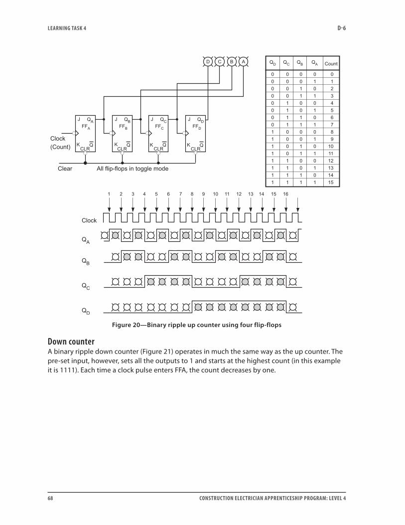
LEARNING TASk 4 D-6
68 CONSTRUCTION ELECTRICIAN APPRENTICESHIP PROGRAM: LEVEL 4
Figure 20—Binary ripple up counter using four flip-flops
Down counterA binary ripple down counter (Figure 21) operates in much the same way as the up counter. The pre-set input, however, sets all the outputs to 1 and starts at the highest count (in this example it is 1111). Each time a clock pulse enters FFA, the count decreases by one.
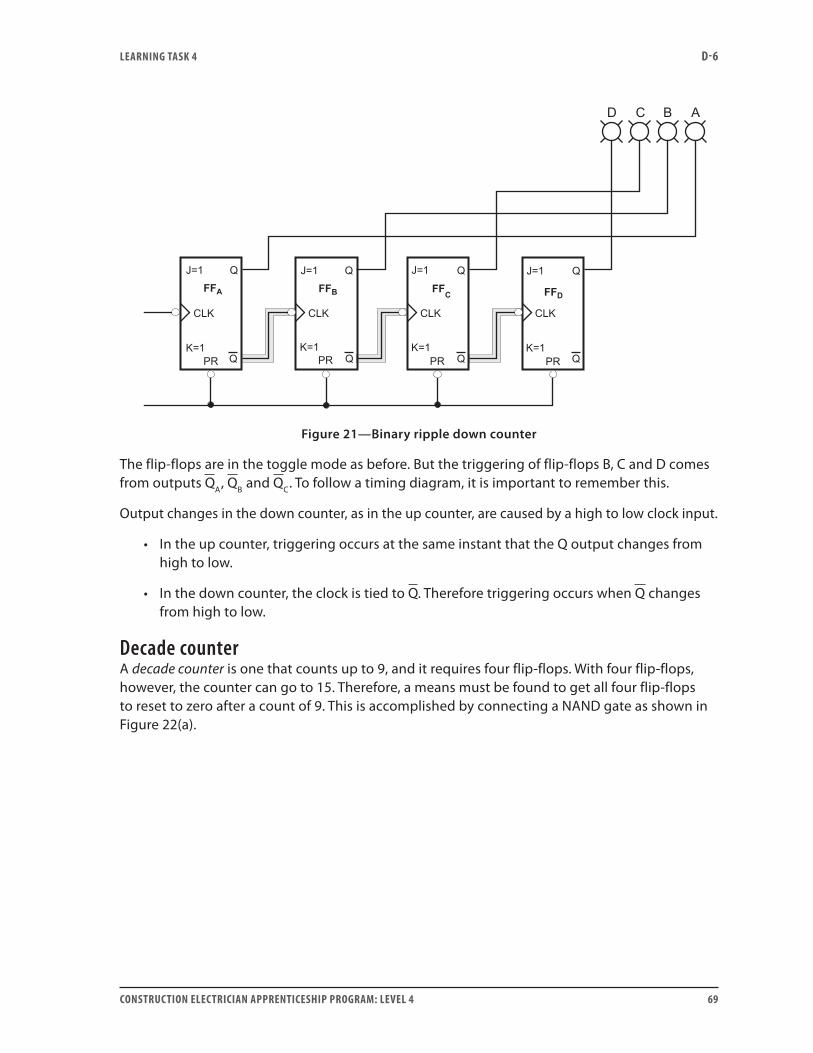
LEARNING TASk 4 D-6
CONSTRUCTION ELECTRICIAN APPRENTICESHIP PROGRAM: LEVEL 4 69
Figure 21—Binary ripple down counter
The flip-flops are in the toggle mode as before. But the triggering of flip-flops B, C and D comes from outputs QA, QB and QC. To follow a timing diagram, it is important to remember this.
Output changes in the down counter, as in the up counter, are caused by a high to low clock input.
• In the up counter, triggering occurs at the same instant that the Q output changes from high to low.
• In the down counter, the clock is tied to Q. Therefore triggering occurs when Q changes from high to low.
Decade counterA decade counter is one that counts up to 9, and it requires four flip-flops. With four flip-flops, however, the counter can go to 15. Therefore, a means must be found to get all four flip-flops to reset to zero after a count of 9. This is accomplished by connecting a NAND gate as shown in Figure 22(a).

LEARNING TASk 4 D-6
70 CONSTRUCTION ELECTRICIAN APPRENTICESHIP PROGRAM: LEVEL 4
Figure 22—Decade counter and binary counting chart
When the NAND output goes low, it acts to clear all the outputs to 0. If you look at the binary count in Figure 22(b), notice that it is only at the count of 10 that the two NAND gate inputs both become 1 simultaneously. This is the condition necessary to make the output of the NAND gate 0. This output of the NAND gate clears the inputs of all four flip-flops. And when a flip-flop gets a 0 on its clear input it “resets” or “clears” its Q to 0.
Notice that the last count to show is 9, or 1001. At the count of 10 the output will be 1010, but at the same instant the NAND gate will clear everything to 0, so 0000 shows up (not 1010). The LEDs connected to QA and QD go on and off at the same instant, so they are not seen to come on at the count of 10.
By connecting a two- or three-input NAND gate to the appropriate Q outputs, the counter can count to any desired number—below the highest count for that counter—then clear and repeat.
Synchronous countersThe propagation delay as the clock signal ripples through each flip-flop in the binary ripple counter is a serious shortcoming. These delays are cumulative and limit its application. Synchronous binary counters operate faster than ripple counters, because the clock input goes to all flip-flops simultaneously (Figure 23). However, they also require more power to operate and they cost more.
The 74LS193 shown in Figure 23 is a very versatile high-speed synchronous counter, with the ability to count up and down.
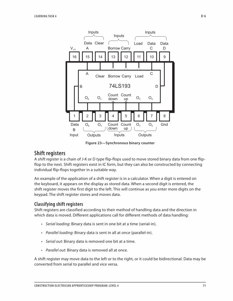
LEARNING TASk 4 D-6
CONSTRUCTION ELECTRICIAN APPRENTICESHIP PROGRAM: LEVEL 4 71
Figure 23—Synchronous binary counter
Shift registersA shift register is a chain of J-K or D type flip-flops used to move stored binary data from one flip-flop to the next. Shift registers exist in IC form, but they can also be constructed by connecting individual flip-flops together in a suitable way.
An example of the application of a shift register is in a calculator. When a digit is entered on the keyboard, it appears on the display as stored data. When a second digit is entered, the shift register moves the first digit to the left. This will continue as you enter more digits on the keypad. The shift register stores and moves data.
Classifying shift registersShift registers are classified according to their method of handling data and the direction in which data is moved. Different applications call for different methods of data handling:
• Serial loading: Binary data is sent in one bit at a time (serial-in).
• Parallel loading: Binary data is sent in all at once (parallel-in).
• Serial out: Binary data is removed one bit at a time.
• Parallel out: Binary data is removed all at once.
A shift register may move data to the left or to the right, or it could be bidirectional. Data may be converted from serial to parallel and vice versa.
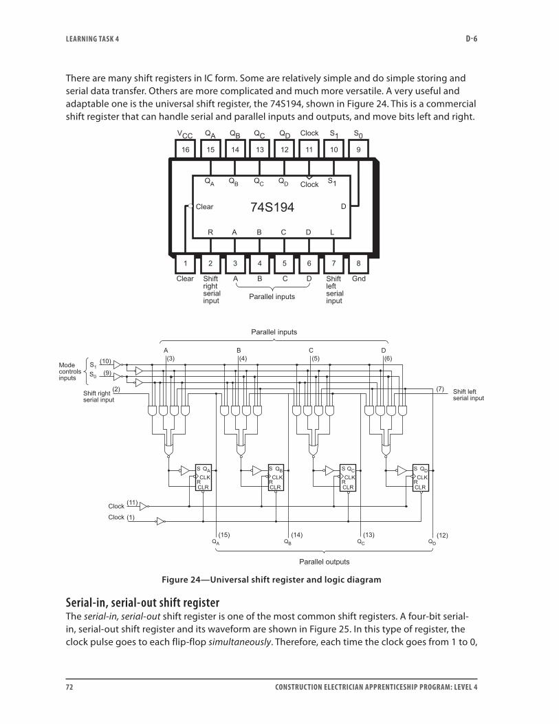
LEARNING TASk 4 D-6
72 CONSTRUCTION ELECTRICIAN APPRENTICESHIP PROGRAM: LEVEL 4
There are many shift registers in IC form. Some are relatively simple and do simple storing and serial data transfer. Others are more complicated and much more versatile. A very useful and adaptable one is the universal shift register, the 74S194, shown in Figure 24. This is a commercial shift register that can handle serial and parallel inputs and outputs, and move bits left and right.
Figure 24—Universal shift register and logic diagram
Serial-in, serial-out shift registerThe serial-in, serial-out shift register is one of the most common shift registers. A four-bit serial-in, serial-out shift register and its waveform are shown in Figure 25. In this type of register, the clock pulse goes to each flip-flop simultaneously. Therefore, each time the clock goes from 1 to 0,
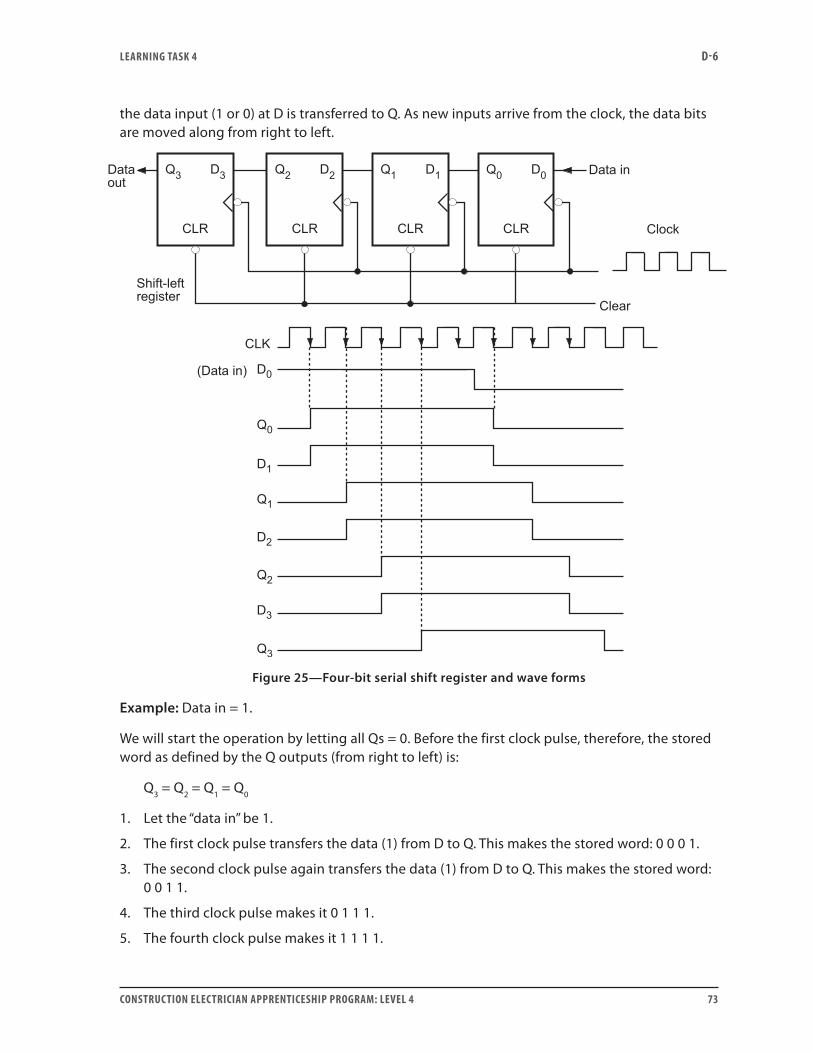
LEARNING TASk 4 D-6
CONSTRUCTION ELECTRICIAN APPRENTICESHIP PROGRAM: LEVEL 4 73
the data input (1 or 0) at D is transferred to Q. As new inputs arrive from the clock, the data bits are moved along from right to left.
Figure 25—Four-bit serial shift register and wave forms
Example: Data in = 1.
We will start the operation by letting all Qs = 0. Before the first clock pulse, therefore, the stored word as defined by the Q outputs (from right to left) is:
Q3 = Q2 = Q1 = Q0
1. Let the “data in” be 1.
2. The first clock pulse transfers the data (1) from D to Q. This makes the stored word: 0 0 0 1.
3. The second clock pulse again transfers the data (1) from D to Q. This makes the stored word: 0 0 1 1.
4. The third clock pulse makes it 0 1 1 1.
5. The fourth clock pulse makes it 1 1 1 1.
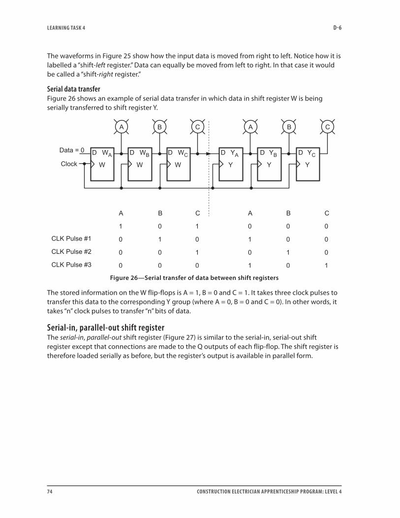
LEARNING TASk 4 D-6
74 CONSTRUCTION ELECTRICIAN APPRENTICESHIP PROGRAM: LEVEL 4
The waveforms in Figure 25 show how the input data is moved from right to left. Notice how it is labelled a “shift-left register.” Data can equally be moved from left to right. In that case it would be called a “shift-right register.”
Serial data transferFigure 26 shows an example of serial data transfer in which data in shift register W is being serially transferred to shift register Y.
Figure 26—Serial transfer of data between shift registers
The stored information on the W flip-flops is A = 1, B = 0 and C = 1. It takes three clock pulses to transfer this data to the corresponding Y group (where A = 0, B = 0 and C = 0). In other words, it takes “n” clock pulses to transfer “n” bits of data.
Serial-in, parallel-out shift registerThe serial-in, parallel-out shift register (Figure 27) is similar to the serial-in, serial-out shift register except that connections are made to the Q outputs of each flip-flop. The shift register is therefore loaded serially as before, but the register’s output is available in parallel form.
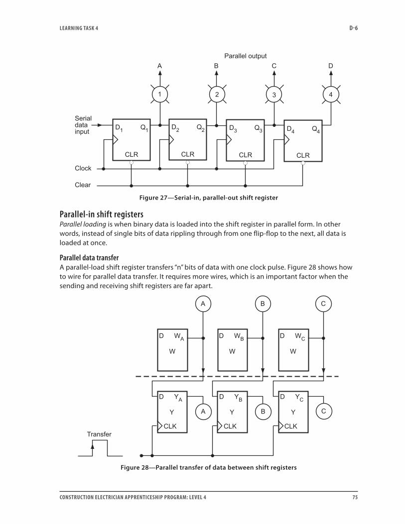
LEARNING TASk 4 D-6
CONSTRUCTION ELECTRICIAN APPRENTICESHIP PROGRAM: LEVEL 4 75
Figure 27—Serial-in, parallel-out shift register
Parallel-in shift registersParallel loading is when binary data is loaded into the shift register in parallel form. In other words, instead of single bits of data rippling through from one flip-flop to the next, all data is loaded at once.
Parallel data transferA parallel-load shift register transfers “n” bits of data with one clock pulse. Figure 28 shows how to wire for parallel data transfer. It requires more wires, which is an important factor when the sending and receiving shift registers are far apart.
Figure 28—Parallel transfer of data between shift registers
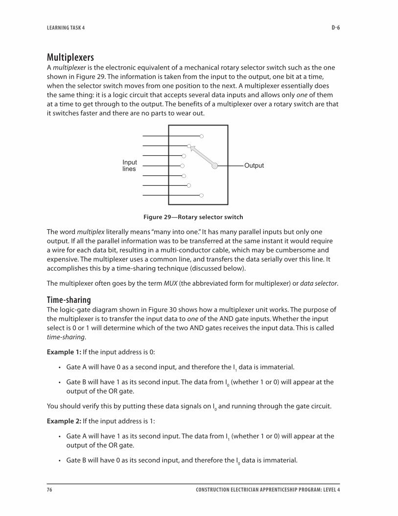
LEARNING TASk 4 D-6
76 CONSTRUCTION ELECTRICIAN APPRENTICESHIP PROGRAM: LEVEL 4
MultiplexersA multiplexer is the electronic equivalent of a mechanical rotary selector switch such as the one shown in Figure 29. The information is taken from the input to the output, one bit at a time, when the selector switch moves from one position to the next. A multiplexer essentially does the same thing: it is a logic circuit that accepts several data inputs and allows only one of them at a time to get through to the output. The benefits of a multiplexer over a rotary switch are that it switches faster and there are no parts to wear out.
Figure 29—Rotary selector switch
The word multiplex literally means “many into one.” It has many parallel inputs but only one output. If all the parallel information was to be transferred at the same instant it would require a wire for each data bit, resulting in a multi-conductor cable, which may be cumbersome and expensive. The multiplexer uses a common line, and transfers the data serially over this line. It accomplishes this by a time-sharing technique (discussed below).
The multiplexer often goes by the term MUX (the abbreviated form for multiplexer) or data selector.
Time-sharingThe logic-gate diagram shown in Figure 30 shows how a multiplexer unit works. The purpose of the multiplexer is to transfer the input data to one of the AND gate inputs. Whether the input select is 0 or 1 will determine which of the two AND gates receives the input data. This is called time-sharing.
Example 1: If the input address is 0:
• Gate A will have 0 as a second input, and therefore the I1 data is immaterial.
• Gate B will have 1 as its second input. The data from I0 (whether 1 or 0) will appear at the output of the OR gate.
You should verify this by putting these data signals on I0 and running through the gate circuit.
Example 2: If the input address is 1:
• Gate A will have 1 as its second input. The data from I1 (whether 1 or 0) will appear at the output of the OR gate.
• Gate B will have 0 as its second input, and therefore the I0 data is immaterial.
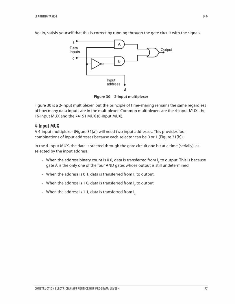
LEARNING TASk 4 D-6
CONSTRUCTION ELECTRICIAN APPRENTICESHIP PROGRAM: LEVEL 4 77
Again, satisfy yourself that this is correct by running through the gate circuit with the signals.
Figure 30—2-input multiplexer
Figure 30 is a 2-input multiplexer, but the principle of time-sharing remains the same regardless of how many data inputs are in the multiplexer. Common multiplexers are the 4-input MUX, the 16-input MUX and the 74151 MUX (8-input MUX).
4-Input MUXA 4-input multiplexer (Figure 31[a]) will need two input addresses. This provides four combinations of input addresses because each selector can be 0 or 1 (Figure 31[b]).
In the 4-input MUX, the data is steered through the gate circuit one bit at a time (serially), as selected by the input address.
• When the address binary count is 0 0, data is transferred from I0 to output. This is because gate A is the only one of the four AND gates whose output is still undetermined.
• When the address is 0 1, data is transferred from I1 to output.
• When the address is 1 0, data is transferred from I2 to output.
• When the address is 1 1, data is transferred from I3.
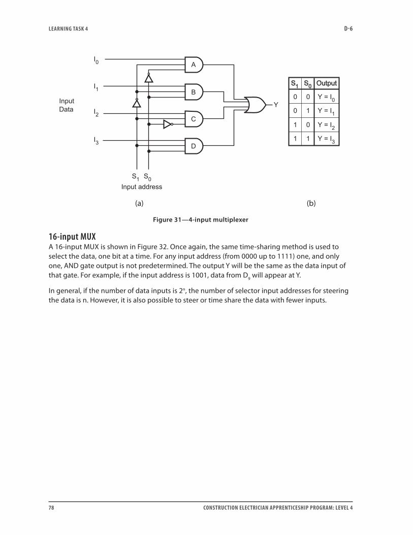
LEARNING TASk 4 D-6
78 CONSTRUCTION ELECTRICIAN APPRENTICESHIP PROGRAM: LEVEL 4
(a) (b)
Figure 31—4-input multiplexer
16-input MUXA 16-input MUX is shown in Figure 32. Once again, the same time-sharing method is used to select the data, one bit at a time. For any input address (from 0000 up to 1111) one, and only one, AND gate output is not predetermined. The output Y will be the same as the data input of that gate. For example, if the input address is 1001, data from D9 will appear at Y.
In general, if the number of data inputs is 2n, the number of selector input addresses for steering the data is n. However, it is also possible to steer or time share the data with fewer inputs.

LEARNING TASk 4 D-6
CONSTRUCTION ELECTRICIAN APPRENTICESHIP PROGRAM: LEVEL 4 79
Figure 32—16-input multiplexer
Now do Self-Test 4 and check your answers.

LEARNING TASk 4 D-6
80 CONSTRUCTION ELECTRICIAN APPRENTICESHIP PROGRAM: LEVEL 4
Self-Test 4
1. What is the more formal name for a flip-flop?
2. Name the four common flip-flops.
3. Which of the flip-flops is most commonly used and is referred to as a latch?
4. For an R-S flip-flop made from NOR gates, what are the outputs Q and Q when S = 0 and R = 1?
5. For an R-S flip-flop made of NAND gates, what S and R inputs put the outputs in memory condition?
6. In a Clocked R-S flip-flop, what clock logic level freezes the outputs?
‘
7. What statement sums up the operation of the D type flip-flop?
8. What must the J and K inputs be for the J-K flip-flop to operate in toggle mode?

LEARNING TASk 4 D-6
CONSTRUCTION ELECTRICIAN APPRENTICESHIP PROGRAM: LEVEL 4 81
9. Consider that the clock frequency input to a J-K flip-flop (operating in toggle mode) is 5000 Hz. What is the output frequency?
10. Identify the three forms of multivibrators.
11. Which of the multivibrators does not require an input signal in order to function?
12. What determines the output frequency of an astable multivibrator?
13. Which multivibrator is also called a one shot?
14. Consider a monostable multivibrator having R = 10 kΩ and C = 100 μF. What is the duration of the pulse (T) in seconds?
15. Draw the output waveform at Q for the D type flip-flop in Figure 1.
Figure 1

LEARNING TASk 4 D-6
82 CONSTRUCTION ELECTRICIAN APPRENTICESHIP PROGRAM: LEVEL 4
16. What devices form the building blocks for counters and shift registers?
17. What is meant by the modulus of a counter?
18. What is the modulus of a binary ripple counter that has five flip-flops?
19. Why is it necessary to have a clear input in an up counter?
20. What is the difference between the up and down binary ripple counters?
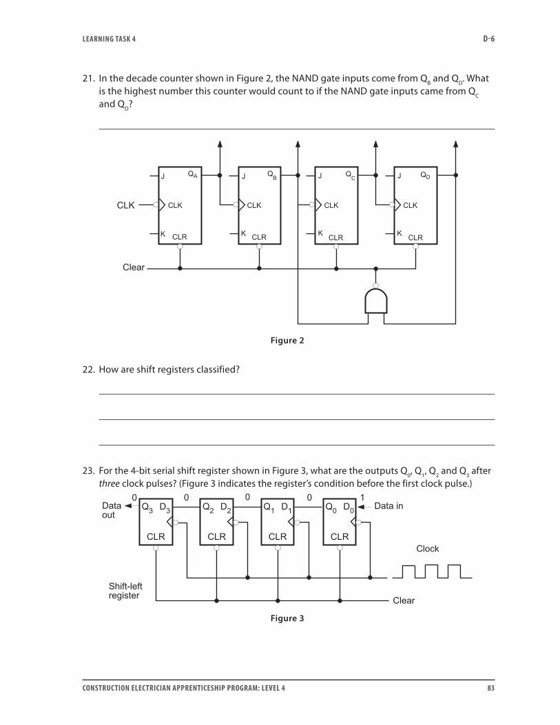
LEARNING TASk 4 D-6
CONSTRUCTION ELECTRICIAN APPRENTICESHIP PROGRAM: LEVEL 4 83
21. In the decade counter shown in Figure 2, the NAND gate inputs come from QB and QD. What is the highest number this counter would count to if the NAND gate inputs came from QC
and QD?
Figure 2
22. How are shift registers classified?
23. For the 4-bit serial shift register shown in Figure 3, what are the outputs Q0, Q1, Q2 and Q3 after three clock pulses? (Figure 3 indicates the register’s condition before the first clock pulse.)
Figure 3

LEARNING TASk 4 D-6
84 CONSTRUCTION ELECTRICIAN APPRENTICESHIP PROGRAM: LEVEL 4
24. The shift register illustrated in Figure 3 is a -in, -out shift register. (serial and/or parallel)
25. A multiplexer is the electronic equivalent of what kind of mechanical switch?
Go to the Answer Key at the end of the Learning Guide to check your answers.

CONSTRUCTION ELECTRICIAN APPRENTICESHIP PROGRAM: LEVEL 4 85
Learning Task 5:
Describe the features of integrated circuits (IC)An IC (integrated circuit) is a complete electronic circuit fabricated on a tiny piece of silicon material. The circuit is so small it requires a microscope to see it. The term integrated circuit is used because there are no interconnecting wires, and the various transistors, resistors, diodes and connections are etched out of a silicon chip.
Prior to the introduction of the first IC in 1958, electronic circuits were assembled by interconnecting individual components with wires. These were (and still are) called discrete circuits. ICs quickly revolutionized the electronics industry. Though initially expensive, the per-unit cost dropped rapidly with volume, mass production and newer fabrication methods. At the same time, the number of components and circuits that could be fabricated on these tiny silicon semiconductor chips increased dramatically.
Comparisons between ICs and discrete circuitsAn IC has several advantages over a discrete circuit.
High reliabilityNo wires to open, short-circuit or become unsoldered, and the circuit is completely encapsulated in a plastic or ceramic package, eliminating corrosion, vibration, etc.
Small sizeHuge developments and reductions in the physical size of electronic components have occurred as a consequence of the IC. And the number of components and circuits that can be fabricated in these devices has risen dramatically over the years.
Low costThe mass production of huge quantities of similar devices makes ICs today considerably less expensive than a discrete component circuit.
High speedHigh speed can be achieved because the distances travelled by electrons in ICs are extremely short compared to those in a discrete component circuit.
Less power consumedPower consumption is reduced because voltage drops and the power loss in the wiring are practically eliminated. As well, the smaller transistors and other components mean lower power drain. This reduction in power also means that less cooling is required.

LEARNING TASk 5 D-6
86 CONSTRUCTION ELECTRICIAN APPRENTICESHIP PROGRAM: LEVEL 4
ICs also have shortcomings:
Current and voltage limitationsCurrents and voltages must be low.
• Currents must be very low because heat built up in such a tiny chip would quickly cause damage.
• Voltages must also be low because it is extremely difficult to insulate components that operate in such close proximity.
For these reasons ICs are essentially for information processing. Operations that require high power levels must still be handled by circuits using discrete components.
Limited component selectionFor the most part, IC circuits consist of transistors, diodes and resistors. Some may even incorporate small capacitors in the chip. But such devices as large capacitors, inductors and transformers are difficult or impossible to fabricate on a chip.
Non-repairableThough ICs are non-repairable, this is hardly a disadvantage, as a faulty IC can be easier to find and replace than discrete components. This reduces labour costs and there is less production down time.
IC classificationICs may be categorized in a few different ways. A common way is to classify an IC as either digital (sometimes called logic) or linear (sometimes called analogue). Each chip is designed for a certain function. You must use data books and manufacturers’ specification sheets to determine the function of a particular IC.
Digital (logic)Digital (or logic) ICs are used mainly for switching applications. Digital circuits perform logic and counting functions by recognizing only high and low signals. These are most commonly used in such things as calculators, computers, PLCs and microprocessors.
Linear (analogue)Linear (or analogue) ICs are primarily used for amplifiers. They respond to signals that vary in amplitude and frequency, which are traditionally found in radio and telecommunication circuits. They vary and control voltages and are most commonly used in amplifiers, oscillators, voltage regulators and operational amplifiers.
Combined digital-linearWhile it is common to classify ICs as being digital or linear, there are also ICs that combine both functions on one chip.
Digital ICs are classified according to the circuit complexity or levels of component integration in the chip. Currently, there are four levels of integration or complexity, defined in Table 1.

LEARNING TASk 5 D-6
CONSTRUCTION ELECTRICIAN APPRENTICESHIP PROGRAM: LEVEL 4 87
Table 1: Four levels of integration
Complexity Number of gates on the same chipSmall-scale integration (SSI) Fewer than 12 Medium-scale integration (MSI) 12 to 99 Large-scale integration (LSI) 100 to 9999 Very large-scale integration (VLSI) 10 000 or more
One other way in which digital ICs are classified is according to the type of transistor used in the IC.
• ICs may use bipolar transistors (NPN or PNP) or field-effect transistors (FETs).
• The TTL logic family uses the bipolar transistor type.
• The CMOS logic family uses the field-effect transistor type.
TTL and CMOS are well-known digital logic families. Each has advantages and disadvantages compared to the other.
TTLTTL is the most widely used of the logic families. Its logic gates use bipolar transistors requiring a +5 V power supply, and its initial identifying characteristic is its high speed. Standard TTL is the general-purpose family of TTL, using the NAND gate as its flagship.
Table 2 summarizes the most common TTL logic sub-families.
Table 2: Sub-families of TTL
Logic sub-family Prefix Propagation delay* (approx.)
Power dissipation per gate (approx.)
Standard TTL 74 10 ns 10 mWLow power TTL 74L 35 ns 1 mW High speed TTL 74H 5 ns 22 mW Schottky TTL 74S 3 ns 20 mWLow power Schottky** 74LS 10 ns 2 mWAdvanced Schottky 74AS 1.7 ns 8 mWAdvanced low power Schottky
74ALS 4 ns 1.2 mW
* Time it takes for an output to respond to a change in input. ** The Schottky 74L and 74H sub-families are becoming obsolete because of their
lower values of speed-power product.
The pin configurations and numbers in all TTL sub-families are the same. For example, a 7408 is a standard TTL quad, 2-input AND gate. (Quad means it contains four identical gates.) The 74H08 is the same quad, 2-input AND gate having identical pinouts, but it belongs to the high speed sub-family.

LEARNING TASk 5 D-6
88 CONSTRUCTION ELECTRICIAN APPRENTICESHIP PROGRAM: LEVEL 4
There are dozens of different manufacturers making these logic families: Texas Instruments, Signetics, National Semiconductor and Motorola, to mention just some of the bigger ones. They prefix their chip numbers by letters such as SN, S, LF and MC, respectively. For example, Texas Instruments makes an IC chip called SN7408. This code indicates it is a TTL, quad, 2-input AND gate IC.
CMOS CMOS is the other large IC family. It gets its name from Complementary Metal Oxide Semiconductor. The field-effect transistors used in CMOS logic gates take up little space, are cheap to manufacture and consume little power. Because they are so small, they are ideally suited for LSI and VLSI (large- and very large-scale integration) IC chips.
The family of MOSFET logic includes P-MOS and N-MOS logic gates. CMOS uses a combination of the transistors from P-MOS and N-MOS to produce a higher speed, lower power requirement chip. The low power drain is a big advantage with equipment that is battery operated. And while its slow speed (relative to TTL) has been a traditional shortcoming, newer CMOS gates are rapidly gaining in switching speeds, and some are as fast as the TTL gates. With higher operating voltages switching speeds increase, but so does power consumption.
CMOS is very susceptible to static electricity, and its extremely thin dielectric can be broken down and destroyed by static charges.
Be careful when handling CMOS logic chips. Static electricity from the human body can break down the dielectric, causing gate destruction.
Table 3 shows some of the characteristics of CMOS chips. The values in the table will vary with operating voltages; they are used here for comparative purposes only.
Table 3: Sub-families of CMOS
Logic sub-family Power dissipation per gate (approx.)
Propagation delay (approx.)
Compatibility with TTL
*pin **electrically
4011 B 5 mW 50 ns *no **no74HC 100 mW 15 ns *yes **no74HCT 100 mW 15 ns *yes **yes
IC constructionIntegrated circuits are constructed by forming transistors, diodes, resistors and even small capacitors on a silicon chip.
An IC can contain as few as several to as many as hundreds of thousands of transistors on a single chip. Individual components are interconnected by aluminum, copper or gold wiring patterns that resemble ordinary printed circuit-board wiring. Tiny gold wires that connect inputs, outputs and power points on the chip are welded under a microscope to pins on the exterior.
A small, highly magnified section of a silicon chip is shown in Figure 1.
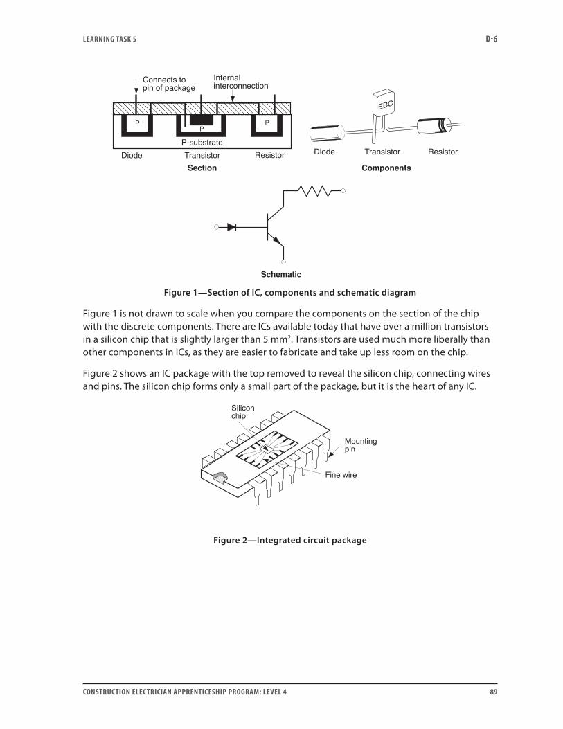
LEARNING TASk 5 D-6
CONSTRUCTION ELECTRICIAN APPRENTICESHIP PROGRAM: LEVEL 4 89
Schematic
Section Components
Connects topin of package
PP
P
Internalinterconnection
Diode Transistor ResistorP-substrate
Diode Transistor Resistor
EBC
Figure 1—Section of IC, components and schematic diagram
Figure 1 is not drawn to scale when you compare the components on the section of the chip with the discrete components. There are ICs available today that have over a million transistors in a silicon chip that is slightly larger than 5 mm2. Transistors are used much more liberally than other components in ICs, as they are easier to fabricate and take up less room on the chip.
Figure 2 shows an IC package with the top removed to reveal the silicon chip, connecting wires and pins. The silicon chip forms only a small part of the package, but it is the heart of any IC.
Siliconchip
Mountingpin
Fine wire
Figure 2—Integrated circuit package
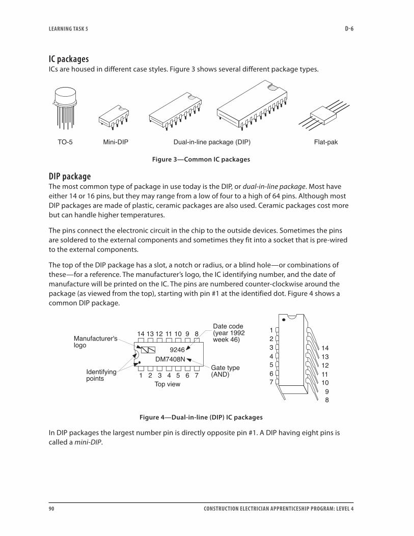
LEARNING TASk 5 D-6
90 CONSTRUCTION ELECTRICIAN APPRENTICESHIP PROGRAM: LEVEL 4
IC packagesICs are housed in different case styles. Figure 3 shows several different package types.
TO-5 Mini-DIP Dual-in-line package (DIP) Flat-pak
Figure 3—Common IC packages
DIP packageThe most common type of package in use today is the DIP, or dual-in-line package. Most have either 14 or 16 pins, but they may range from a low of four to a high of 64 pins. Although most DIP packages are made of plastic, ceramic packages are also used. Ceramic packages cost more but can handle higher temperatures.
The pins connect the electronic circuit in the chip to the outside devices. Sometimes the pins are soldered to the external components and sometimes they fit into a socket that is pre-wired to the external components.
The top of the DIP package has a slot, a notch or radius, or a blind hole—or combinations of these—for a reference. The manufacturer’s logo, the IC identifying number, and the date of manufacture will be printed on the IC. The pins are numbered counter-clockwise around the package (as viewed from the top), starting with pin #1 at the identified dot. Figure 4 shows a common DIP package.
14 13 12 11 10 9 8
1 2 3 4 5 6 7
9246DM7408N
Manufacturer'slogo
Date code(year 1992week 46)
Gate type(AND)
1234567
1413121110
98
Top view
Identifyingpoints
Figure 4—Dual-in-line (DIP) IC packages
In DIP packages the largest number pin is directly opposite pin #1. A DIP having eight pins is called a mini-DIP.
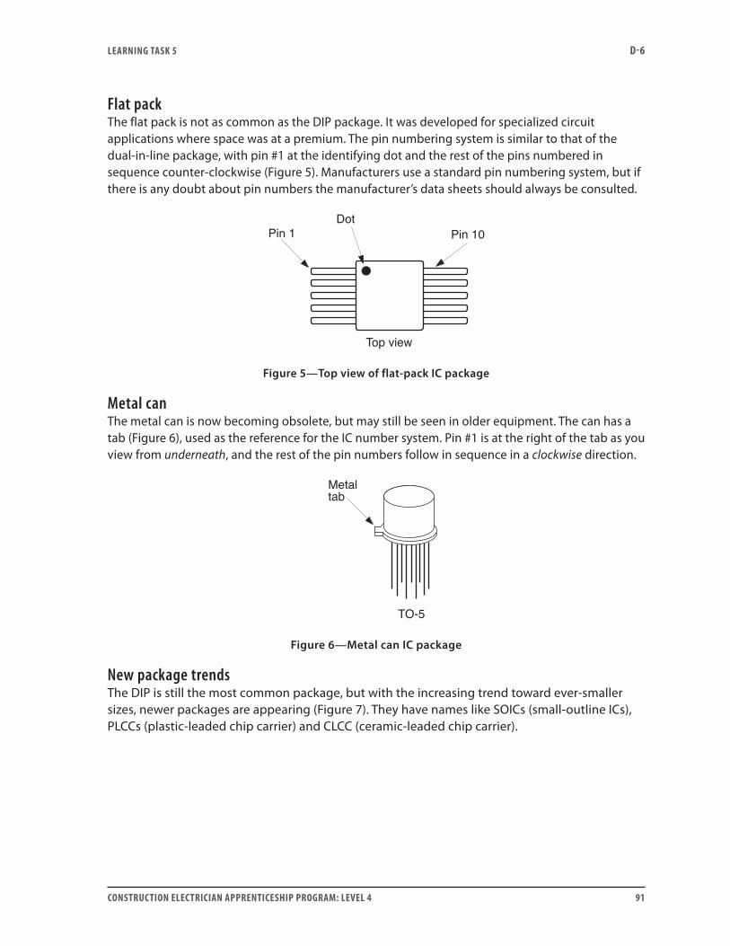
LEARNING TASk 5 D-6
CONSTRUCTION ELECTRICIAN APPRENTICESHIP PROGRAM: LEVEL 4 91
Flat packThe flat pack is not as common as the DIP package. It was developed for specialized circuit applications where space was at a premium. The pin numbering system is similar to that of the dual-in-line package, with pin #1 at the identifying dot and the rest of the pins numbered in sequence counter-clockwise (Figure 5). Manufacturers use a standard pin numbering system, but if there is any doubt about pin numbers the manufacturer’s data sheets should always be consulted.
Pin 10Dot
Pin 1
Top view
Figure 5—Top view of flat-pack IC package
Metal canThe metal can is now becoming obsolete, but may still be seen in older equipment. The can has a tab (Figure 6), used as the reference for the IC number system. Pin #1 is at the right of the tab as you view from underneath, and the rest of the pin numbers follow in sequence in a clockwise direction.
Metaltab
TO-5
Figure 6—Metal can IC package
New package trendsThe DIP is still the most common package, but with the increasing trend toward ever-smaller sizes, newer packages are appearing (Figure 7). They have names like SOICs (small-outline ICs), PLCCs (plastic-leaded chip carrier) and CLCC (ceramic-leaded chip carrier).
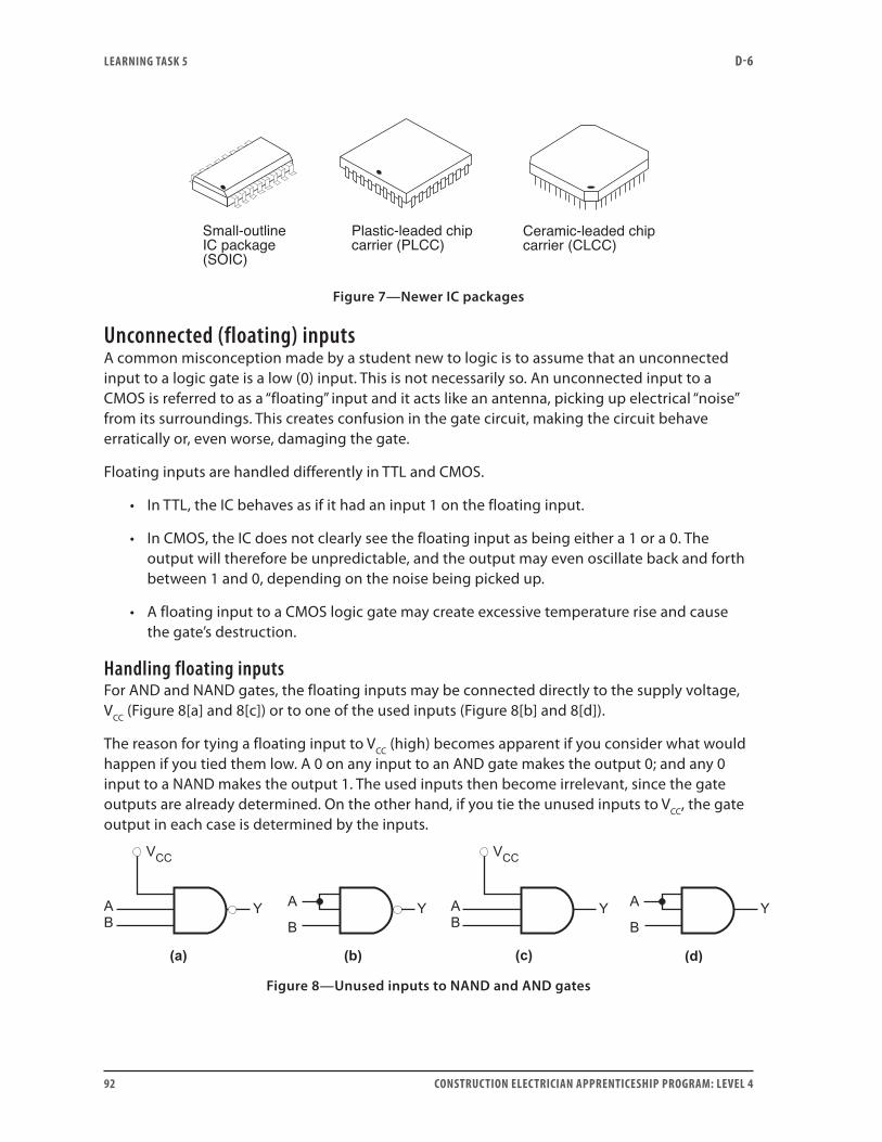
LEARNING TASk 5 D-6
92 CONSTRUCTION ELECTRICIAN APPRENTICESHIP PROGRAM: LEVEL 4
Small-outlineIC package(SOIC)
Plastic-leaded chipcarrier (PLCC)
Ceramic-leaded chipcarrier (CLCC)
Figure 7—Newer IC packages
Unconnected (floating) inputsA common misconception made by a student new to logic is to assume that an unconnected input to a logic gate is a low (0) input. This is not necessarily so. An unconnected input to a CMOS is referred to as a “floating” input and it acts like an antenna, picking up electrical “noise” from its surroundings. This creates confusion in the gate circuit, making the circuit behave erratically or, even worse, damaging the gate.
Floating inputs are handled differently in TTL and CMOS.
• In TTL, the IC behaves as if it had an input 1 on the floating input.
• In CMOS, the IC does not clearly see the floating input as being either a 1 or a 0. The output will therefore be unpredictable, and the output may even oscillate back and forth between 1 and 0, depending on the noise being picked up.
• A floating input to a CMOS logic gate may create excessive temperature rise and cause the gate’s destruction.
Handling floating inputsFor AND and NAND gates, the floating inputs may be connected directly to the supply voltage, VCC (Figure 8[a] and 8[c]) or to one of the used inputs (Figure 8[b] and 8[d]).
The reason for tying a floating input to VCC (high) becomes apparent if you consider what would happen if you tied them low. A 0 on any input to an AND gate makes the output 0; and any 0 input to a NAND makes the output 1. The used inputs then become irrelevant, since the gate outputs are already determined. On the other hand, if you tie the unused inputs to VCC, the gate output in each case is determined by the inputs.
Figure 8—Unused inputs to NAND and AND gates
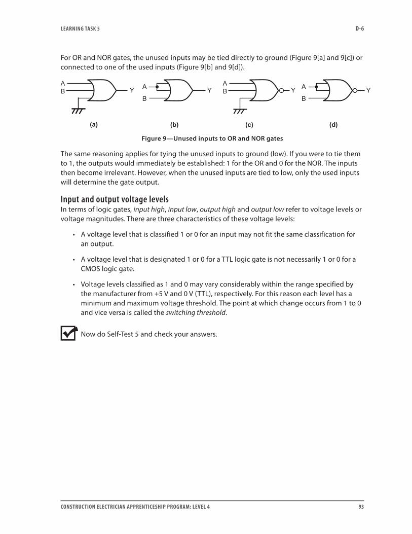
LEARNING TASk 5 D-6
CONSTRUCTION ELECTRICIAN APPRENTICESHIP PROGRAM: LEVEL 4 93
For OR and NOR gates, the unused inputs may be tied directly to ground (Figure 9[a] and 9[c]) or connected to one of the used inputs (Figure 9[b] and 9[d]).
Figure 9—Unused inputs to OR and NOR gates
The same reasoning applies for tying the unused inputs to ground (low). If you were to tie them to 1, the outputs would immediately be established: 1 for the OR and 0 for the NOR. The inputs then become irrelevant. However, when the unused inputs are tied to low, only the used inputs will determine the gate output.
Input and output voltage levelsIn terms of logic gates, input high, input low, output high and output low refer to voltage levels or voltage magnitudes. There are three characteristics of these voltage levels:
• A voltage level that is classified 1 or 0 for an input may not fit the same classification for an output.
• A voltage level that is designated 1 or 0 for a TTL logic gate is not necessarily 1 or 0 for a CMOS logic gate.
• Voltage levels classified as 1 and 0 may vary considerably within the range specified by the manufacturer from +5 V and 0 V (TTL), respectively. For this reason each level has a minimum and maximum voltage threshold. The point at which change occurs from 1 to 0 and vice versa is called the switching threshold.
Now do Self-Test 5 and check your answers.

LEARNING TASk 5 D-6
94 CONSTRUCTION ELECTRICIAN APPRENTICESHIP PROGRAM: LEVEL 4
Self-Test 5
1. Prior to the introduction of the integrated circuit, electronic circuits were made using
components.
2. Name five advantages of the integrated circuit as compared to its predecessor.
3. Identify two limitations of ICs.
4. ICs may be classified into two categories. They are:
5. Digital ICs may be classified according to the number of logic gates on the same chip. From the lowest to the highest they are called:
6. The TTL logic family uses transistors, and the CMOS family uses
transistors.

LEARNING TASk 5 D-6
CONSTRUCTION ELECTRICIAN APPRENTICESHIP PROGRAM: LEVEL 4 95
7. ICs are made from what well-known semiconductor material?
8. How many pins does a mini-DIP have?
9. Identify the pin numbers in the IC shown in Figure 1.
Figure 1
10. In a DIP, where is the highest pin number located relative to pin #1?
11. Which type of IC package is now becoming obsolete?
12. What advantage does a DIP housed in a ceramic package have over the plastic package?
13. Which of the two logic families has the faster switching speed?
14. Which logic family is noted for its low power draw?

LEARNING TASk 5 D-6
96 CONSTRUCTION ELECTRICIAN APPRENTICESHIP PROGRAM: LEVEL 4
15. Which logic family is most susceptible to damage from static electricity?
16. Should an unused input to an OR gate be tied high or low?
17. Should an unused input to a NAND gate be tied high or low?
18. If an unused input of a TTL gate is left floating, what will happen?
19. If an unused input of a CMOS is left floating, what may happen?
Go to the Answer Key at the end of the Learning Guide to check your answers.

CONSTRUCTION ELECTRICIAN APPRENTICESHIP PROGRAM: LEVEL 4 97
Learning Task 6:
Connect and test digital logic circuitsTesting digital logic circuitsCommon tools used to troubleshoot digital logic circuits are the:
• Logic probe
• Logic pulser
• Oscilloscope (digital voltmeters may be used in place of oscilloscopes in some circuits)
In some respects digital circuits are easier to troubleshoot than linear circuits, because all you need to know is whether there is a high or a low (0 or 1) at some point in the circuit. The actual numerical voltage at that point is not important. Therefore, logic probes that indicate a 1 or a 0 at some point in a circuit suffice for troubleshooting. Keep in mind, however, that 1s and 0s represent different voltage levels, since logic families use different voltages.
Logic probeA logic probe (Figure 1) is a necessary digital testing tool. It is powered from a DC source by way of two small, flexible leads with alligator clips. This is the voltage that is used to test the ICs.
The probe has two LEDs, one green and the other red.
• The red LED lights up when the probe touches any part of a gate or circuit that is high or logic 1.
• The green LED lights up when the probe touches any part of a gate or circuit that is low or logic 0.
Figure 1—Logic probe
The probe has a selector switch marked TTL and CMOS, and sometimes a PULSE/MEM LED.

LEARNING TASk 6 D-6
98 CONSTRUCTION ELECTRICIAN APPRENTICESHIP PROGRAM: LEVEL 4
Selector switch on TTLA TTL logic gate recognizes voltages equal to or greater than (≥) 2 V as input 1, and voltages between 0 V and 0.8 V as input 0. With the selector switch on TTL, therefore:
• The green LED lights up if the logic probe is touching a point that has a voltage of up to 0.8 V with respect to ground.
• The red LED lights up if the logic probe is touching a point that has a voltage of 2 V or higher with respect to ground.
When neither LED lights, or one lights dimly, the voltage is between 0.8 V and 2 V. This is in the undefined voltage zone, which means either a bad high level or a bad low level and suggests there is a problem at that point in the circuit. Absence of an LED light could, of course, also mean an open circuit.
Selector switch on CMOSWith the selector switch on CMOS:
• The green LED lights up if the circuit voltage is 30% of the supply voltage.
• The red LED lights if the circuit voltage is 70% of the supply voltage.
These voltages are defined as percentages because CMOS power supply voltage can vary between 2 V and 18 V.
Pulse/mem LEDBesides providing TTL and CMOS level sensing, many logic probes have a third (yellow) LED, with PULSE/MEM indicated beside it. This LED serves two purposes:
• On PULSE, the yellow LED will blink on and off when the probe is on a rectangular or square wave signal.
Since the red and green LEDs go on and off at high speed in a high-frequency digital signal, the human eye may see both as being on. The yellow LED therefore blinks on and off with an intensity that is proportional to the duty cycle of this signal. (The display pulse rate, however, is much lower than the actual rate.)
• On MEM, the pulse LED is put into memory.
In the MEM position, the yellow LED latches ON with the first rising or falling pulse.
Logic pulserA logic pulser (Figure 2) looks similar to a probe, but it can generate a digital pulse when the button on its side is pushed. Each time the button is pressed it generates a high-to-low level pulse. Holding it down generates a continuous pulse train at a frequency of 100 Hz.
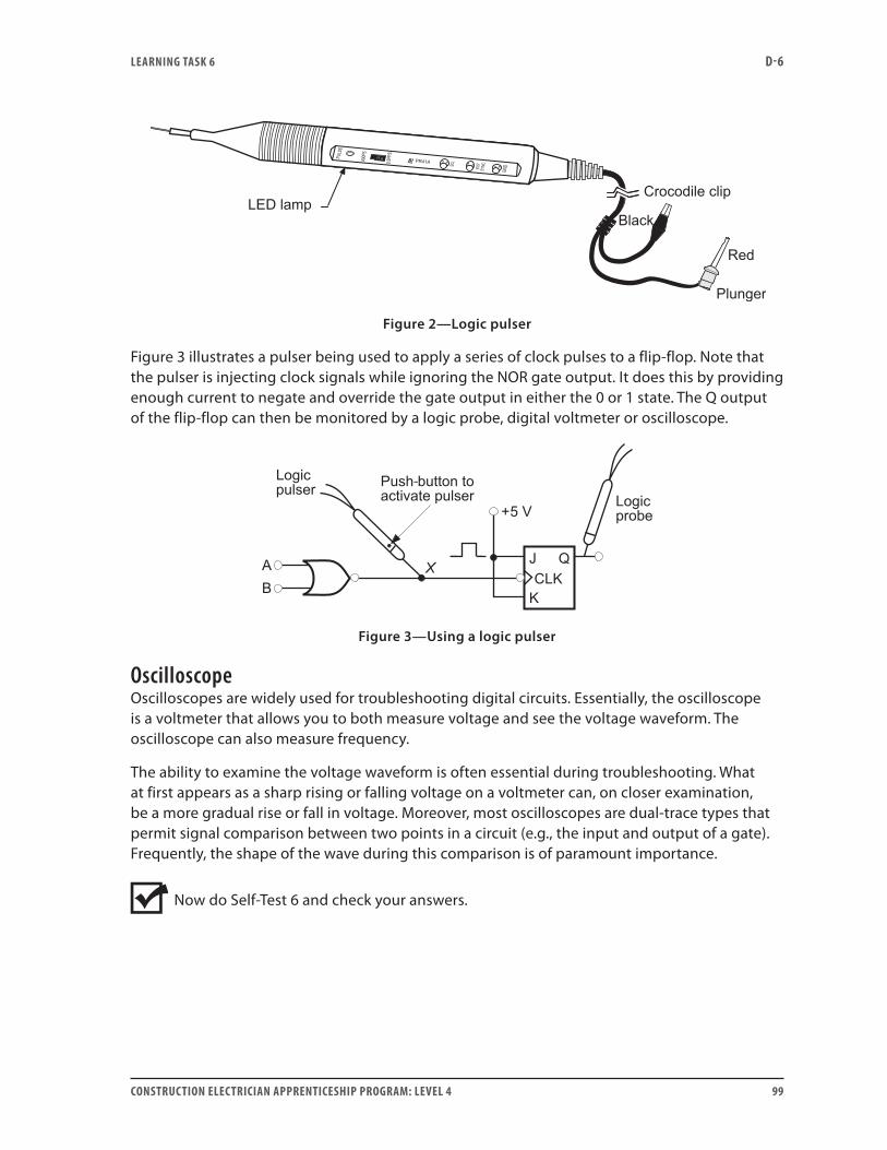
LEARNING TASk 6 D-6
CONSTRUCTION ELECTRICIAN APPRENTICESHIP PROGRAM: LEVEL 4 99
Figure 2—Logic pulser
Figure 3 illustrates a pulser being used to apply a series of clock pulses to a flip-flop. Note that the pulser is injecting clock signals while ignoring the NOR gate output. It does this by providing enough current to negate and override the gate output in either the 0 or 1 state. The Q output of the flip-flop can then be monitored by a logic probe, digital voltmeter or oscilloscope.
-
Figure 3—Using a logic pulser
OscilloscopeOscilloscopes are widely used for troubleshooting digital circuits. Essentially, the oscilloscope is a voltmeter that allows you to both measure voltage and see the voltage waveform. The oscilloscope can also measure frequency.
The ability to examine the voltage waveform is often essential during troubleshooting. What at first appears as a sharp rising or falling voltage on a voltmeter can, on closer examination, be a more gradual rise or fall in voltage. Moreover, most oscilloscopes are dual-trace types that permit signal comparison between two points in a circuit (e.g., the input and output of a gate). Frequently, the shape of the wave during this comparison is of paramount importance.
Now do Self-Test 6 and check your answers.

LEARNING TASk 6 D-6
100 CONSTRUCTION ELECTRICIAN APPRENTICESHIP PROGRAM: LEVEL 4
Self-Test 6
1. How does a logic probe indicate the presence of a logic 1 in a circuit?
2. If either one of the LEDs on a logic probe is lighting dimly, what does it suggest?
3. What is the purpose of the yellow LED associated with the PULSE/MEM selector switch?
4. A logic probe receives its supply from an internal battery.
a. True
b. False
5. What is a logic pulser used for?
6. Digital voltmeters can only measure pulse voltages.
a. True
b. False
7. What quantities can the oscilloscope measure?
8. What advantage does an oscilloscope have over a digital voltmeter?
Go to the Answer Key at the end of the Learning Guide to check your answers.

CONSTRUCTION ELECTRICIAN APPRENTICESHIP PROGRAM: LEVEL 4 101
Learning Task 7:
Describe the features of operational amplifiers
Operational amplifiersAn operational amplifier, or op-amp, is basically a linear (analogue) amplifier. It was originally used for high-gain DC amplification in conjunction with analogue computers. Nowadays, it is still widely used for high-gain DC amplification, but it also has many applications in analogue/digital interfacing circuits.
The op-amp is a low-current, low-voltage, low-power integrated circuit device that has a gain in the region of 200 000 and higher. Op-amps frequently use external feedback to control their responses and reduce the gain. They are widely used in television, radio and telecommunications, as well as in industrial applications.
There are many varieties of op-amp circuits on the market. Manufacturer’s data sheets specify the voltage, current and operating characteristics. A typical rating is 15 V, 20 mA, 300 mW, and it usually comes in a dual-inline, integrated circuit (IC) package.
Op-amp symbolThe schematic symbol for the op-amp is shown in Figure 1. The op-amp has two inputs and one output.
The inputs are called inverting (–) and non-inverting (+) inputs. If the + is grounded, the output signal is 180º out of phase with the input signal. If the – is grounded, the output signal is 0º, or in phase, with the input signal (Figure 2).
Output
Output
Input
Input
Figure 2—Inverting and non-inverting modes
Output signalInput signal
Input signal
Figure 1—Op-amp symbol
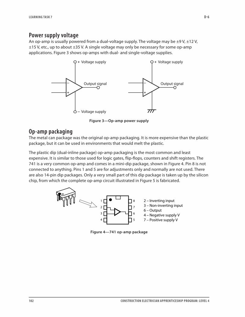
LEARNING TASk 7 D-6
102 CONSTRUCTION ELECTRICIAN APPRENTICESHIP PROGRAM: LEVEL 4
Power supply voltageAn op-amp is usually powered from a dual-voltage supply. The voltage may be ±9 V, ±12 V, ±15 V, etc., up to about ±35 V. A single voltage may only be necessary for some op-amp applications. Figure 3 shows op-amps with dual- and single-voltage supplies.
Output signal
Voltage supply
Voltage supply
Output signal
Voltage supply
Figure 3—Op-amp power supply
Op-amp packagingThe metal can package was the original op-amp packaging. It is more expensive than the plastic package, but it can be used in environments that would melt the plastic.
The plastic dip (dual-inline package) op-amp packaging is the most common and least expensive. It is similar to those used for logic gates, flip-flops, counters and shift registers. The 741 is a very common op-amp and comes in a mini-dip package, shown in Figure 4. Pin 8 is not connected to anything. Pins 1 and 5 are for adjustments only and normally are not used. There are also 14-pin dip packages. Only a very small part of this dip package is taken up by the silicon chip, from which the complete op-amp circuit illustrated in Figure 5 is fabricated.
Figure 4—741 op-amp package
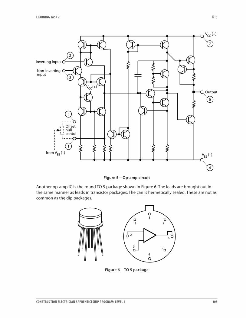
LEARNING TASk 7 D-6
CONSTRUCTION ELECTRICIAN APPRENTICESHIP PROGRAM: LEVEL 4 103
Figure 5—Op-amp circuit
Another op-amp IC is the round TO 5 package shown in Figure 6. The leads are brought out in the same manner as leads in transistor packages. The can is hermetically sealed. These are not as common as the dip packages.
Figure 6—TO 5 package

LEARNING TASk 7 D-6
104 CONSTRUCTION ELECTRICIAN APPRENTICESHIP PROGRAM: LEVEL 4
The flat pack op-amp package (Figure 7) is a plastic package, similar to the dip packages, except the pins extend outward rather than downward as in the dip package. Another plastic package uses a staggered pinout formation.
Figure 7—Flat pack
Open- and closed-loop op-ampsAn op-amp is a high-gain amplifier. It may be operated in open- or closed-loop configuration.
Open-loopIn the open-loop mode the gain is very high but unstable, upward of 200 000 for the 741 op-amp. However, this high gain is not of much use in many cases because the output voltage can never exceed the power supply voltage. In practice, the output will saturate at one or two volts below the power supply voltage.
Closed-loopClosed-loop means there is feedback from the output back to the inverting input. The gain is substantially lower in this connection (but is more stable over a range of frequencies), and it can be controlled by means of external resistors.
Differential amplifierOne primary application of an op-amp is as a differential amplifier that measures the difference between two input signals. This difference is then amplified at the output. It is important to note that it is not the individual signals that are amplified; it is the difference that is amplified. The differential amplifier is connected in an open-loop configuration. In Figure 8 the difference between V1 and V2 is amplified.
Figure 8—Op-amp as a differential amplifier

LEARNING TASk 7 D-6
CONSTRUCTION ELECTRICIAN APPRENTICESHIP PROGRAM: LEVEL 4 105
Op-amp comparatorThe comparator application is similar to that of the differential amplifier in that two input signals are compared and the difference is amplified. However, one of the signals is a fixed reference voltage, and the output always goes into saturation. The other input signal is the feedback voltage, coming, for example, from a tachometer on a motor shaft. Minute differences between the reference voltage and the feedback voltage will drive the output into saturation. This output then acts to make a change or correction. In this case, the correction is to increase or decrease the speed of the motor. There are many industrial applications for the comparator circuit, where varying input voltages must be compared to reference voltages, and changes effected.
Figure 9 shows how the op-amp comparator works. We will assume that the output saturates at +10 V and –10 V for this supply voltage. The op-amp is in the open-loop configuration.
Vout = +10 V
12 V
12 V
Vout = –10 V
12 V
12 V
Rin
Rin
Figure 9—Comparator action
When Vin is positive with respect to ground, the output will saturate to +10 V (Figure 10). If Vin is negative with respect to ground, the output will saturate at –10 V. Because the open-loop gain is so high, Vin need be only slightly more positive or negative to cause output saturation.
Figure 10—Comparator circuit
Vin is compared to a reference voltage that is adjustable. The output will adjust or correct the output device by way of a signal to a relay, thyristor, transistor or other amplifier stage.

LEARNING TASk 7 D-6
106 CONSTRUCTION ELECTRICIAN APPRENTICESHIP PROGRAM: LEVEL 4
Squaring a sine waveIf the reference voltage is zero (Figure 11), the op-amp acts to turn a sine wave into a square wave.
Figure 11—Converting a sine wave to a square wave
The op-amp amplifies the voltage difference between the reference voltage (0 V) and the feedback voltage. Because the difference then becomes the reference (sine wave) voltage, and the amplification in open-loop is so high, the moment the voltage rises above or below zero, the output voltage reaches saturation.
Now do Self-Test 7 and check your answers.

LEARNING TASk 7 D-6
CONSTRUCTION ELECTRICIAN APPRENTICESHIP PROGRAM: LEVEL 4 107
Self-Test 7
1. Draw the symbol for an op-amp.
2. What is the most common op-amp package?
3. The power rating of a typical op-amp is about (500 W, 100 W, 1 W, 300 mW).
4. Match the following pin with numbers on the 741 op-amp in Figure 1.
Pin number
Inverting input
Non-inverting input
Output
Positive V supply
Negative V supply
5. When comparing the op-amp in open-loop and closed-loop modes, which has the higher gain, or is there any difference?
741
1
2
3
4
8
7
6
5
Figure 1

LEARNING TASk 7 D-6
108 CONSTRUCTION ELECTRICIAN APPRENTICESHIP PROGRAM: LEVEL 4
6. How is the gain of the op-amp controlled?
7. In a differential amplifier, what is amplified?
8. What are the names of the input signals in the op-amp comparator?
9. What is the purpose of the op-amp comparator circuit?
10. The output voltage of the op-amp comparator reaches what magnitude?
Go to the Answer Key at the end of the Learning Guide to check your answers.

CONSTRUCTION ELECTRICIAN APPRENTICESHIP PROGRAM: LEVEL 4 109
Learning Task 8:
Describe common circuit applications for the operational amplifier
Voltage-followerIn the voltage-follower application (Figure 1), the op-amp gain is unity, or 1. In other words, there is no gain; the output and input signals are identical. The op-amp is operating in the manner of a 1:1 isolating transformer. It acts as a buffer device, isolating the input signal source from the connected load at the output. The purpose is to reduce the loading effect that a low-resistance load will have on a weak signal source.
An op-amp has very high input impedance and low output impedance. This means that the load receives the signal, while the op-amp serves to avoid signal source loading. Also, because the output impedance of the op-amp is low, the load is driven by a voltage source that has a very low internal impedance, which is always a desirable feature.
Figure 1—Voltage-follower
Inverting amplifierFigure 2 shows the op-amp connected for operation as an inverting amplifier. The non-inverting input is grounded and the input signal goes to the inverting input. With this connection, the output signal will be inverted, or 180º out-of-phase with the input signal. The gain of the amplifier is the ratio of Rf, the feedback resistor, to Rin, the input resistor. The gain, or amplification, in closed-loop is identified as “Acl.”
Figure 2—Inverting amplifier
LEARNING TASk 8 D-6
110 CONSTRUCTION ELECTRICIAN APPRENTICESHIP PROGRAM: LEVEL 4
Point P in Figure 2 is considered to be at virtual ground, which means the voltage across the + and – input terminals can be taken to be zero. Current can be assumed to be the same value through Rin and Rf.
From this it can be shown that the gain:
ARRcl
f
in
=
Since:
AVV
and ARRcl
out
incl
f
in
= =
It follows that:
Vout = –Vin
Rf
Rin
(minus sign indicates that the output is inverted)
Example: If the input voltage was 0.5 Vp–p, Rin = 1 kΩ, and Rf = 5.6 kΩ, what would be the output voltage?
Solution:
ARR
5.6 Ω1.0 kΩ
5.6clf
in
= = =k
Since:
Vout = –Vin × Acl
Then:
V
V
out
p p
= ×
= −
0 5 5 6
2 8
. .
.
Non-inverting amplifierIn the non-inverting amplifier hookup (Figure 3), the connection is similar to that of the inverting amplifier, but notice that the input signal goes to the non-inverting terminal. The resistor at the inverting terminal has one side connected to ground, and the feedback resistor connects between the output and the other side of the input resistor as with the inverting amplifier. The voltage across the + and – input terminals can be considered zero, as it is with the inverting amplifier.
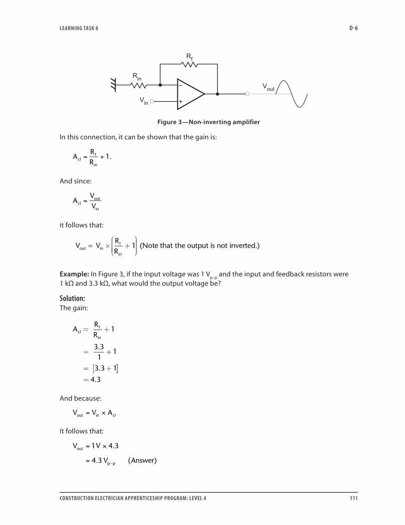
LEARNING TASk 8 D-6
CONSTRUCTION ELECTRICIAN APPRENTICESHIP PROGRAM: LEVEL 4 111
Figure 3—Non-inverting amplifier
In this connection, it can be shown that the gain is:
ARRcl
f
in
= + 1.
And since:
AVVclout
in
=
it follows that:
Vout = Vin
Rf
Rin
+ 1 (Note that the output is not inverted.)
Example: In Figure 3, if the input voltage was 1 Vp–p and the input and feedback resistors were 1 kΩ and 3.3 kΩ, what would the output voltage be?
Solution:The gain:
ARRcl
f
in
= +
= +
= +[
1
3 31
1
3 3 1
.
. ]]= 4 3.
And because:
V V Aout in cl= ×
It follows that:
V 1V 4.3
4.3 V Answer)
out
p p
= ×
= − (

LEARNING TASk 8 D-6
112 CONSTRUCTION ELECTRICIAN APPRENTICESHIP PROGRAM: LEVEL 4
Summing amplifierIn the summing amplifier connection (Figure 4), the op-amp adds together two or more voltages at the inputs, and amplifies them at the output.
The output voltage cannot exceed (or even reach) that of the power supply voltage. For this reason, the input voltages must be less than the power supply voltage to the op-amp.
Figure 4—Summing amplifier connection
Vout = V1
Rf
R1
+ V2
Rf
R2
+ V3
Rf
R3
(i) If R1 = R2 = R3 = Rf then Vout = – V1 + V2 + V3( )
(ii) If R1 = R2 = R3 and Rf = kR1 then Vout = –k V1 + V2 + V3( )
where k = Rf
Rin
(iii) The weighting given to each signal can be adjusted by varying R1, R2 and R3.
(iv) If R1 = R2 = R3 = 3Rf then Vout = average of the three input voltages
Op-amp integratorAn op-amp integrator is a useful but specialized circuit. The integrator and differentiator op-amp circuits are complementary and perform mathematical functions. (Do not confuse differential op-amp with differentiator op-amp). Differentiating and integrating are mathematical operations that determine rate-of-change and areas under a curve (wave shape), respectively. Figure 5 shows a basic op-amp integrator circuit, though in practice this circuit would have to be somewhat modified.
By proper selection of the external components, an op-amp integrator may be used to output a desired triangular-shaped wave from a digital input signal. Or, the integrator can produce a phase-shift (other than 0º or 180º) between an input and output sine wave.

LEARNING TASk 8 D-6
CONSTRUCTION ELECTRICIAN APPRENTICESHIP PROGRAM: LEVEL 4 113
Figure 5—Op-amp integrator circuit
Digital-to-analogue converter (DAC)Digital-to-analogue converters turn digital signals into analogue signals. The digital input signals are in the form of 0s and 1s (taken from devices such as flip-flops, counters and computers) representing 0 V and 5 V, respectively. The operation of the DAC is based on the summing amplifier principle, shown in Figure 6.
Figure 6—Op-amp digital-to-analogue converter
The weighting given to the input resistors must be binary-related. That is, 20(1), 21(2), 22(4), 23(8) and so on. The resistors, like binary digits, double from one to the next. The inputs A, B, C and D are either 0 V or 5 V. You will recall that the summing amplifier multiplies each input voltage by the ratio of the feedback resistor to the input resistor on that input. Each digital input contributes a different voltage magnitude to the output, and its weight depends on its location in the binary position. The LSB in the binary inputs is the A and the MSB is D. The output voltages reflect this, as shown in the circuit.

LEARNING TASk 8 D-6
114 CONSTRUCTION ELECTRICIAN APPRENTICESHIP PROGRAM: LEVEL 4
Let’s begin with a digital input of 1111 and look at the output:
1 A = – 5 V840
= –1V
1 B = – 5 V820
= –2 V
1 C = – 5 V810
= –4 V
1 D = – 5 V85
= –8 V
= –15 V
And if the digital input were 1011 the output would be:
1 A = – 5 V840
= –1V
1 B = – 5 V820
= –2 V
0 C = – 0 V8
10= 0 V
1 D = – 5 V85
= –8 V
= –11V
Because the outputs of digital devices are only nominal 0 V and 5 V, and could vary considerably, precision-level amplifiers must be used to make the voltages exactly 0 and 5 V. This is shown in Figure 7.

LEARNING TASk 8 D-6
CONSTRUCTION ELECTRICIAN APPRENTICESHIP PROGRAM: LEVEL 4 115
Figure 7—DAC with precision-level amplifiers
Analogue-to-digital converter (ADC)The opposite of the DAC is the analogue-to-digital converter, which turns analogue signals into digital signals. An example of the operation of an ADC is shown in the circuit in Figure 8. Notice the polarity of the LEDs. Resistors R1 to R5 form a voltage divider. This puts a reference voltage on each non-inverting input, as shown. Recall that in an op-amp comparator, the output saturates to one or the other extreme of the op-amp power supply. In this case, it is 0 V or +5 V. If the + input is higher than the – input, the output will saturate at +5 V and the LED will stay off. But if the + input is lower than the – input, the output will be 0 V and the LED will be on.

LEARNING TASk 8 D-6
116 CONSTRUCTION ELECTRICIAN APPRENTICESHIP PROGRAM: LEVEL 4
Vin(analogue input)
Figure 8—Analogue-to-digital conversion
With Vin at 3.5 V, LEDs 1, 2 and 3 light, but 4 stays off. If the LEDs are arranged vertically (as a set of windows) as shown in Figure 9, the bar display will indicate a digital signal of 3 V.
This is a fairly coarse circuit because the bar graph can only sense voltage differences of 1 V. However, it could be refined by using more op-amps and reference voltage resistors. If there were eight op-amps and eight reference voltage resistors (and eight LEDs), each LED in the graph would light at every 0.5 V increment in input analogue voltage. This is called improving the resolution.
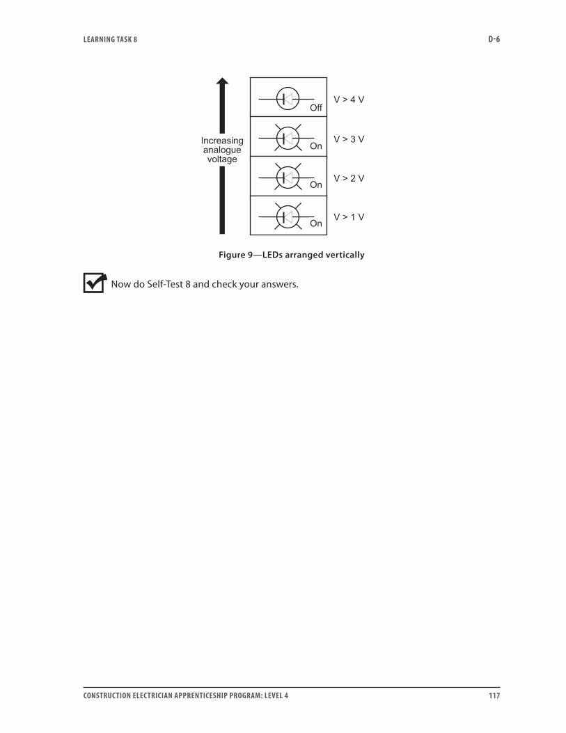
LEARNING TASk 8 D-6
CONSTRUCTION ELECTRICIAN APPRENTICESHIP PROGRAM: LEVEL 4 117
Figure 9—LEDs arranged vertically
Now do Self-Test 8 and check your answers.

LEARNING TASk 8 D-6
118 CONSTRUCTION ELECTRICIAN APPRENTICESHIP PROGRAM: LEVEL 4
Self-Test 8
1. In the op-amp voltage-follower, the output compared with the input is (higher/
lower/identical) and (in-phase/inverted).
2. The voltage-follower is often used as a(n) (switching/amplifying/buffer) device
between a (high/low) impedance source and a (high/low) impedance
load.
3. Calculate the output voltage for the inverting op-amp in Figure 1.
Vout
+1.5 VR1
Rf = 10 kΩ
2.2 kΩ P
Figure 1
4. Calculate the output voltage for the non-inverting op-amp in Figure 2.
Vout
R1= 5 kΩ
Rf = 40 kΩ
Vin = 1.2 V
Figure 2
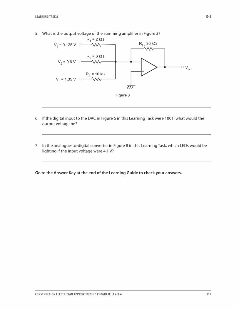
LEARNING TASk 8 D-6
CONSTRUCTION ELECTRICIAN APPRENTICESHIP PROGRAM: LEVEL 4 119
5. What is the output voltage of the summing amplifier in Figure 3?
Figure 3
6. If the digital input to the DAC in Figure 6 in this Learning Task were 1001, what would the output voltage be?
7. In the analogue-to-digital converter in Figure 8 in this Learning Task, which LEDs would be lighting if the input voltage were 4.1 V?
Go to the Answer Key at the end of the Learning Guide to check your answers.

120 CONSTRUCTION ELECTRICIAN APPRENTICESHIP PROGRAM: LEVEL 4
CONSTRUCTION ELECTRICIAN APPRENTICESHIP PROGRAM: LEVEL 4 121
Answer key
Self-Test 11. Decimal uses base 10, binary uses base 2, octal uses base 8, hexadecimal uses base 16.
2. a. 27 b. 276 c. 1000 d. 4702 e. 10010
3. a. 15 b. 5 c. 19 d. 28 e. 21
4. a. 33 b. 276 c. 999 d. 4701 e. 6075
5. a. 1011102 b. 10011012 c. 110112
6. a. 1A716 b. D616 c. 7216
7. 960B16
8. 0010111111102
9. b. false
10. 0001100110000100BCD
11. 248
12. alphanumeric
13. American Standard Code for Information Interchange
14. 1001101
15. There is only ever a one-bit change in consecutive numbers.
Self-Test 21.
2. inverter
3. 0
4. All inputs must be 1 (or high).

ANSwER kEY D-6
122 CONSTRUCTION ELECTRICIAN APPRENTICESHIP PROGRAM: LEVEL 4
5. high
6. A + B + C = Y
7. an AND and a NOT gate
8. 0
9. a. series
10. b. parallel
11. d. complementary
12. A ⊕ B = Y or AB + AB = Y
13. A
B
A
BY Y& ≥1
)b( )a(
14.
AB
Y
15. AB
HLHL
HL
Self-Test 31. two
2.

ANSwER kEY D-6
CONSTRUCTION ELECTRICIAN APPRENTICESHIP PROGRAM: LEVEL 4 123
3.
4. a. Y = (A • B) + C
b. Y = (A + B) • C • D • E
5. A AY Y
Booleanexpression Y = A • B • C
DeMorganequivalent
Gate circuit
6. • Change the operator.
• Negate the inputs and output.
7.
8. d. greater than 4
9. A and C are ON; B and D are OFF.
10. A = 0, B = 1, C = 1 and D = 0
11. All LEDs are OFF because the input is invalid.
Self-Test 41. bistable multivibrator
2. R-S; Clocked R-S; D type; J-K flip-flop
3. R-S
4. Q = 0 and = 1

ANSwER kEY D-6
124 CONSTRUCTION ELECTRICIAN APPRENTICESHIP PROGRAM: LEVEL 4
5. S = R = 1
6. Clock = 0
7. Q follows D, on the arrival of a clock signal
8. J = K =1
9. 2500 Hz
10. astable; bistable; monostable
11. astable
12. the values of the externally connected capacitor and resistor group
13. the monostable multivibrator
14. 1.1 s
15.
16. flip-flops
17. the number of different states a counter goes through before it repeats
18. 32
19. Because all flip-flops must be cleared, or reset, to zero before the count starts.
20. • The down counter flip-flops get their clock signal from the Q output of the previous flip-flop.
• The up counter flip-flops get their clock signal from the Q output.
21. It would count to 11 and then repeat.
22. according to their method of inputting and outputting digital information

ANSwER kEY D-6
CONSTRUCTION ELECTRICIAN APPRENTICESHIP PROGRAM: LEVEL 4 125
23.
24. serial, serial
25. selector switch
Self-Test 51. discrete
2. high reliability; low power drain; high speed; low cost; small size
3. • Confined to low voltage and current applications
• Limited component selection
4. • Digital (logic)
• Linear (analogue)
5. • Small-scale integration (SSI)
• Medium-scale integration (MSI)
• Large-scale integration (LSI)
• Very large-scale integration (VLSI)
6. bipolar; field-effect
7. silicon
8. eight

ANSwER kEY D-6
126 CONSTRUCTION ELECTRICIAN APPRENTICESHIP PROGRAM: LEVEL 4
9.
76
54
32 1
89
1011
121314
10. directly opposite pin #1
11. metal can
12. Ceramic package can handle higher temperatures than plastic.
13. TTL
14. CMOS
15. CMOS
16. low
17. high
18. It will act like a 1.
19. Chip may be destroyed.
Self-Test 61. The red LED lights up.
2. The logic level is in the undefined region.
3. • To indicate a rectangular-shaped waveform
• To detect the rise or fall of a pulse
4. a. False
5. To inject a digital 1 or 0 into a point on a circuit
6. b. False
ANSwER kEY D-6
CONSTRUCTION ELECTRICIAN APPRENTICESHIP PROGRAM: LEVEL 4 127
7. voltage and frequency
8. The waveform, which could be the most crucial factor when troubleshooting, appears on a screen.
Self-Test 71.
2. dual-inline
3. 300 mW
4.
Pin number
Inverting input 2
Non-inverting input 3
Output 6
Positive V supply 7
Negative V supply 4
5. Open-loop gain is higher.
6. by using external resistors
7. the difference between the two input signals
8. reference and feedback
9. To compare a feedback voltage signal with some reference voltage and amplify the difference, in order to make adjustments when necessary. It can also be used to make a square wave from a sine wave.
10. power supply voltage (saturation) level

ANSwER kEY D-6
128 CONSTRUCTION ELECTRICIAN APPRENTICESHIP PROGRAM: LEVEL 4
Self-Test 81. identical, in-phase
2. buffer, high, low
3. –6.82 V
4. 10.8 V
5. –8.925 V
6. –9.0 V
7. all LEDs


ISBN 978-0-7726-6859-2
9 780772 6685927960003644