controllable growth, microstructure and electronic
TRANSCRIPT
HAL Id: tel-01754623https://hal.univ-lorraine.fr/tel-01754623
Submitted on 30 Mar 2018
HAL is a multi-disciplinary open accessarchive for the deposit and dissemination of sci-entific research documents, whether they are pub-lished or not. The documents may come fromteaching and research institutions in France orabroad, or from public or private research centers.
L’archive ouverte pluridisciplinaire HAL, estdestinée au dépôt et à la diffusion de documentsscientifiques de niveau recherche, publiés ou non,émanant des établissements d’enseignement et derecherche français ou étrangers, des laboratoirespublics ou privés.
Controllable growth, microstructure and electronicstructure of copper oxide thin films
Yong Wang
To cite this version:Yong Wang. Controllable growth, microstructure and electronic structure of copper oxide thin films.Other. Université de Lorraine, 2015. English. �NNT : 2015LORR0146�. �tel-01754623�

AVERTISSEMENT
Ce document est le fruit d'un long travail approuvé par le jury de soutenance et mis à disposition de l'ensemble de la communauté universitaire élargie. Il est soumis à la propriété intellectuelle de l'auteur. Ceci implique une obligation de citation et de référencement lors de l’utilisation de ce document. D'autre part, toute contrefaçon, plagiat, reproduction illicite encourt une poursuite pénale. Contact : [email protected]
LIENS Code de la Propriété Intellectuelle. articles L 122. 4 Code de la Propriété Intellectuelle. articles L 335.2- L 335.10 http://www.cfcopies.com/V2/leg/leg_droi.php http://www.culture.gouv.fr/culture/infos-pratiques/droits/protection.htm
THÈSE Pour l’obtention du titre de
DOCTEUR de L’UNIVERSITÉ DE LORRAINE Science et Ingénierie des Matériaux
Présentée par : Yong WANG
Controllable growth, microstructure and electronic
structure of copper oxide thin films
Thèse soutenue publiquement le 16 Novembre à Nancy devant le jury composé de:
Prof. Pierre-Yves JOUAN Institut des Matériaux de Nantes, Université de
Nantes (Nantes) Examinateur
Prof. Christian MOTZ Lehrstuhl für Experimentelle Methodik der Werkstoffwissenschaften, Universität Des Saarlandes (Saarbrücken)
Examinateur
Dr. David MUNOZ-ROJAS Laboratoire des Matériaux et du Génie Physique, CNRS (Grenoble)
Examinateur
Dr. Jaafar GHANBAJA
Institut Jean Lamour, Université de Lorraine (Nancy)
Examinateur
Prof. Panos PATSALAS Department of Materials Science and Engineering, University of Loannina (Greece)
Rapporteur
Prof. Antoine BARNABE CIRIMAT-LCMIE, Université Paul Sabatier (Toulouse)
Rapporteur
Prof. Jean-François PIERSON Institut Jean Lamour, Université de Lorraine (Nancy)
Directeur de Thèse
Prof. Frank MÜCKLICH Lehrstuhl für Funktionswerkstoffe, Universität Des Saarlandes (Saarbrücken)
Co-directeur de Thèse
Institut Jean Lamour –UMR 7198- Département CP2S – Equipe 202 EFCM
Parc de Saurupt - CS 50840- 54011 NANCY Cedex
Université de Lorraine – Pôle M4 : matière, matériaux, métallurgie, mécanique


Controllable growth, microstructure and electronic
structure of copper oxide thin films DISSERTATION zur Erlangung des des Doktorgrades der Ingenieurwissenschaften der Naturwissenschaftlich-Technischen Fakult¨at III Chemie, Pharmazie, Bio- und Werkstoffwissenschaften der Universität Des Saarlandes
von Yong Wang Nancy (France) in 16. November 2015
Tag des Kolloquiums: November, 16th 2015 Dekan:……………………. Prof. Dr. Volkhard Helms -Berichterstatter:…… Prof. Frank MÜCKLICH Lehrstuhl für Funktionswerkstoffe, Universität Des Saarlandes (Saarbrücken) Prof. Christian MOTZ Lehrstuhl für Experimentelle Methodik der Werkstoffwissenschaften, Universität Des Saarlandes (Saarbrücken) Prof. Jean-François PIERSON Institut Jean Lamour, Université de Lorraine (Nancy)
Vorsitz: ……………….. Prof. Pierre-Yves JOUAN Institut des Matériaux de Nantes, Université de Nantes
(Nantes) -Mitglieder des Prüfungsausschusses: Prof. Panos PATSALAS Department of Materials Science and Engineering,
University of Loannina (Greece) Prof. Antoine BARNABE CIRIMAT-LCMIE, Université Paul Sabatier
(Toulouse) Dr. Jaafar GHANBAJA Institut Jean Lamour, Université de Lorraine (Nancy)
Dr. David MUNOZ-ROJAS Laboratoire des Matériaux et du Génie Physique, CNRS (Grenoble)

书山有路勤为径 学海无涯苦作舟
There is no royal road to learning.
Yu Han
To my family,
To all the people who cared for me.


vii
Acknowledgements
This thesis includes most of my three years’ work. A lot of people contributed to my work by
different ways. At this point, I would like to express my appreciation to all of them.
First of all, I wish to express my gratitude to my supervisor Jean-François Pierson for
providing me the opportunity to develop this work. He was always willing to share any ideas
with me. Only through his fruitful discussion, strong experience and hard work, the
completion of this thesis became possible. I remember that he usually replied my email in the
midnight.
I would further like to thank the co-supervisor Frank Mücklich for his important contribution
in my work, as well as the great help during my staying in Saarbrücken.
I especially want to thank Jaafar Ghanbaja for the TEM and EELS measurements. I always
had the easy access to reserve the microscopy. His valuable work and suggestions in TEM
certainly improved the quality of my work.
I would like to thank Stephan Lany for his great contributions to the first-principle
calculations, as well as the insightful and valuable discussions. With his help, I have better
understanding in electronic structure of semiconductor.
I also want to express my great thanks to Flavio Soldera for his TEM sample preparation by
FIB always in a short time, as well as his kind help for my working in Saarland University.
I am particularly grateful for the assistance of Pascal Boulet for the X-ray diffraction
measurements, including Pole figure, detexture and Phi scan. His insightful suggestions
always give me useful and new indicators.
I also would like to thank Thomas Hauet for the PPMS and SQUID measurements and many
discussions. With his help, the room temperature ferromagnetism has been observed in copper

viii
oxide thin films. Even though the part is not presented in the thesis as the origin of
ferromagnetism is still unclear, I believe it really opens a new pathway to understand the
dilute magnetic semiconductor.
I would like to thank David Horwat a lot for his fruitful discussion and manuscript corrections.
I also appreciate the help from Sylvie Migot-Choux and Stéphanie Bruyerè for TEM, Yannick
Fagot-Revurat for XPS/UPS, Patrice Miska for PL, Ander Mézin for stress measurements and
Denis Mangin for SIMS measurements.
In the case of administration, I am grateful for the help from Valérie Tamburini and Martine
Talleur. With the help of Valérie Tamburini, cost in the conference or travel always comes to
my bank account on time.
I am indebted to all the people in PVD group, like David Pilloud, Nolwenn Tranvouez, Alan
Corvisier, Fabien Capon, Alexis Boileau, William Chamorro, Manuel Tresse, Martin Mickan,
Emile Haye, Aurélien Didelot, and Fahad Alnjiman, as well as the Honyuan Zhang and
Aurore Andrieux from other groups. As I cannot speak French, they provide me a lot of help
in work and life.
Thanks the lab Institut Jean Lamour to give me the access to use so many equipments. Three
years’ work here in Nancy, France, with happiness and sadness, will be a beautiful memory in
my life. Wherever in the future, I appreciate the help from all the people.
I also would like to thank the European Commission for ‘Erasmus Mundus’ PhD fellowship
with the DocMASE project.
Finally, I appreciate the special support from my family, as every year I only spend short time
with them.
À Nancy,
15/07/2015

ix
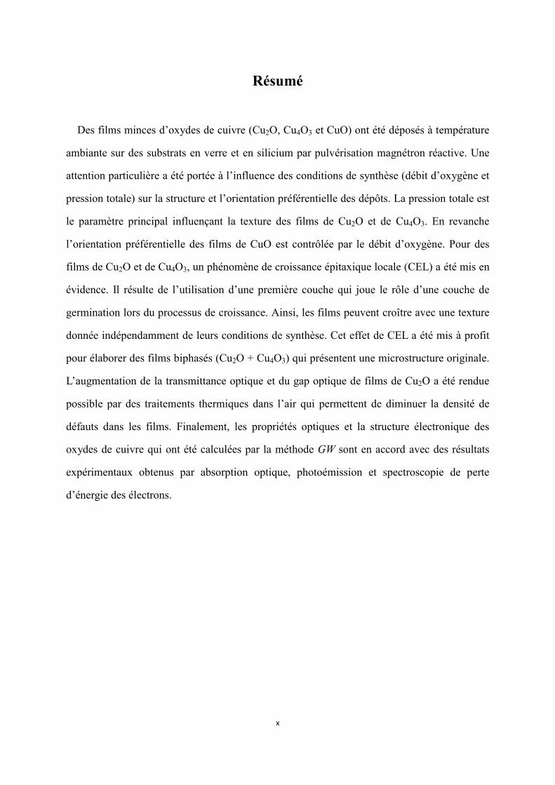
Abstract
Copper oxide (Cu2O, Cu4O3 and CuO) thin films have been deposited on unmatched
substrates by sputtering at room temperature. The influence of oxygen flow rate and total
pressure on the film structure and preferred orientation has been studied. The total pressure is
a relevant parameter to control the texture of Cu2O and Cu4O3 films, while the oxygen flow
rate is effective to tune the preferred orientation of CuO films. Local epitaxial growth, where
epitaxial relationship exists in columns of sputtered films, has been observed in Cu2O and
Cu4O3 films by using a seed layer. The seed layer will govern the growth orientation of top
layer via the local epitaxy, independently of the deposition conditions of top layer. Unusual
microstructure that both phases have the vertically aligned columnar growth has been
evidenced in biphase Cu2O and Cu4O3, which may relate to the local homoepitaxial growth of
Cu2O. The lower resistivity than that in single phase films has been observed in this biphase
film. Annealing in air can increase the transmittance of Cu2O films in visible region by the
reduction of the impurity scattering, while the optical band gap is enlarged due to the partial
removal of defect band tail. The optical properties and electronic structure of copper oxides
calculated by GW approach with an empirical on-site potential for Cu d orbital, are in good
accordance with experimental results from optical absorption, photoemission and electron
energy loss spectroscopies.
x
Résumé
Des films minces d’oxydes de cuivre (Cu2O, Cu4O3 et CuO) ont été déposés à température
ambiante sur des substrats en verre et en silicium par pulvérisation magnétron réactive. Une
attention particulière a été portée à l’influence des conditions de synthèse (débit d’oxygène et
pression totale) sur la structure et l’orientation préférentielle des dépôts. La pression totale est
le paramètre principal influençant la texture des films de Cu2O et de Cu4O3. En revanche
l’orientation préférentielle des films de CuO est contrôlée par le débit d’oxygène. Pour des
films de Cu2O et de Cu4O3, un phénomène de croissance épitaxique locale (CEL) a été mis en
évidence. Il résulte de l’utilisation d’une première couche qui joue le rôle d’une couche de
germination lors du processus de croissance. Ainsi, les films peuvent croître avec une texture
donnée indépendamment de leurs conditions de synthèse. Cet effet de CEL a été mis à profit
pour élaborer des films biphasés (Cu2O + Cu4O3) qui présentent une microstructure originale.
L’augmentation de la transmittance optique et du gap optique de films de Cu2O a été rendue
possible par des traitements thermiques dans l’air qui permettent de diminuer la densité de
défauts dans les films. Finalement, les propriétés optiques et la structure électronique des
oxydes de cuivre qui ont été calculées par la méthode GW sont en accord avec des résultats
expérimentaux obtenus par absorption optique, photoémission et spectroscopie de perte
d’énergie des électrons.
xi
Zusammenfassung
Kupferoxiddünnschichten (Cu2O, Cu4O3 und CuO) wurden selektiv auf amorphen
Substraten durch Sputtern von einem Kupfertarget bei Raumtemperatur abgeschieden. Der
Einfluss der Sauerstoffflussrate und des Gesamtdrucks auf die Schichtstruktur wurde
untersucht. Der Gesamtdruck kontrolliert die Textur von Cu2O und Cu4O3 Schichten, während
die Sauerstoffflussrate die bevorzugte Orientierung von CuO Schichten beeinflusst. Lokales
epitaktisches Wachstum kann genutzt werden um die Wachstumsrichtung der Schichten zu
kontrollieren. Eine Saatschicht steuert die Wachstumsrichtung der oberen Schicht über
epitaktisches kolumnares Wachstum unabhängig von den Abscheidungskonditionen der
oberen Schicht. In Zweiphasen Cu2O und Cu4O3 Schichten wurde vertikal ausgerichtetes
kolumnares Wachstum in beiden Phasen nachgewiesen. Diese ungewöhnliche Mikrostruktur
hängt mit dem lokalen epitaktischen Wachstum von Cu2O zusammen. In den
Zweiphasenschichten wurde eine höhere Leitfähigkeit als in Einphasenschichten beobachtet.
Wärmebehandlung an Luft kann die Transmission von Cu2O Schichten im sichtbaren
Spektrum durch die Reduktion von Streuung an Verunreinigungen erhöhen, während die
optische Bandlücke durch die partielle Entfernung des Defektbands vergrößert wird. Die
durch den GW-Ansatz berechneten optischen Eigenschaften und Bandstrukturen von
Kupferoxiden sind in guter Übereinstimmung mit den experimentellen Ergebnissen der
optischen Absorption, Photoemission und Elektronenenergieverlustspektroskopie.

xii

xiii
Contents Acknowledgements .......................................................................................... vii Abstract ..........................................................................................................ix
Résumé ............................................................................................................. x
Zusammenfassung .............................................................................................xi Contents ....................................................................................................... xiii Introduction ..................................................................................................... 1
Chapter 1 Basic properties of copper oxides and their application in low cost solar cells ...................................................................................................................... 3
1.1 Introduction ............................................................................................ 3
1.2 Basic physical properties of copper oxides ..................................................... 3
1.2.1 Crystal structure ................................................................................. 3
1.2.2 Optical properties and band structures ..................................................... 8
1.2.2.1 Cu2O .......................................................................................... 8
1.2.2.2 Cu4O3 ...................................................................................... 10
1.2.2.3 Monoclinic CuO ......................................................................... 11
1.2.2.4 Tetragonal CuO .......................................................................... 12
1.2.3 Electrical properties and defect mechanism ............................................. 13
1.2.4 Debating issues ................................................................................ 16
1.2.4.1 n-type Cu2O: fact or fiction? .......................................................... 16
1.2.4.2 Oxygen vacancy charge in Cu2O: positive or neutral? .......................... 17
1.3 Synthesis methods .................................................................................. 17
1.4 Recent progress of copper oxides based solar cells ......................................... 18
1.4.1 Advantages of copper oxides ............................................................... 18
1.4.2 Poor performance of Cu2O-based solar cells ........................................... 19
1.5 Chapter conclusions ................................................................................ 22 Chapter 2 Experimental and calculational details .............................................. 23
2.1 Introduction .......................................................................................... 23
2.2 Thin film growth .................................................................................... 23
2.3 Thin film characterization ........................................................................ 27
xiv
2.3.1 X-ray diffraction .............................................................................. 27
2.3.2 Raman spectrometry .......................................................................... 28
2.3.3 Hall effect measurements ................................................................... 28
2.3.4 Transmission electron microscopy ........................................................ 29
2.3.5 Electron energy loss spectroscopy ........................................................ 30
2.3.6 Photoemission spectroscopy ................................................................ 32
2.4 Theoretical calculation method .................................................................. 33
2.5 Chapter conclusions ................................................................................ 34 Chapter 3 Tuning the structure and preferred orientation in reactively sputtered copper oxide thin films ..................................................................................... 35
3.1 Introduction .......................................................................................... 35
3.2 Structure of copper oxide thin films ............................................................ 36
3.2.1 Effect of the oxygen flow rate .............................................................. 36
3.2.2 Effect of the total pressure .................................................................. 38
3.3 Tuning the preferred orientation in copper oxide thin films............................... 40
3.3.1 Effect of the substrate nature ............................................................... 40
3.3.2 Preferred orientation of Cu2O thin films ................................................. 41
3.3.3 Preferred orientation of Cu4O3 thin films ................................................ 43
3.3.4 Preferred orientation of CuO thin films .................................................. 44
3.3.5 Discussion about the preferred orientation in copper oxide thin films ............ 47
3.4 Evidence of a local homoepitaxial growth mechanism in copper oxide thin films .. 49
3.4.1 Study of Cu2O thin films .................................................................... 49
3.4.2 Can the local homoepitaxial growth be extended to Cu4O3 or CuO? .............. 55
3.5 Local heteroepitaxial growth of NiO on Cu2O ............................................... 60
3.6 Chapter conclusions ................................................................................ 68 Chapter 4 Self-assembled growth of vertically aligned columnar copper oxide nanocomposite thin films on unmatched substrates ............................................... 71
4.1 Introduction .......................................................................................... 71
4.2 Vertically aligned columnar growth in biphase Cu2O and Cu4O3 thin films ........... 72
4.2.1 Identifying the phases by X-ray diffraction and Raman spectrometry ............ 72
4.2.2 Cross-sectional microstructure of biphase Cu2O and Cu4O3 thin films ........... 73
4.2.3 Top-view microstructure of biphase Cu2O and Cu4O3 thin films................... 76

xv
4.2.3 Discussion on the vertically aligned columnar growth mechanism ................ 78
4.3 Electrical properties of biphase Cu2O + Cu4O3 thin films ................................. 81
4.4 Chapter Conclusions ............................................................................... 82 Chapter 5 Optical properties and electronic structure of copper oxide thin films ..... 83
5.1 Introduction .......................................................................................... 83
5.2 Transmittance enhancement and optical bandgap widening of Cu2O thin films after air annealing ..................................................................................................... 85
5.2.1 Phase structure evolution ....................................................................... 85
5.2.2 Transmittance enhancement of air annealed Cu2O thin films ....................... 86
5.2.3 Band gap widening of air annealed Cu2O thin films .................................. 88
5.2.4 Photoluminesence analyses on Cu2O thin films ........................................ 91
5.3 Electronic structure of binary copper oxide thin films ..................................... 92
5.3.1 Band gap ........................................................................................ 92
5.3.2 Valence band electronic structure ......................................................... 96
5.3.3 XPS core level and EELS spectra ....................................................... 101
5.3.4 Conduction band electronic structure ................................................... 104
5.4 Chapter conclusions .............................................................................. 106 Conclusions and outlook ................................................................................. 109
Bibliography ................................................................................................ 113
Publications ................................................................................................. 127
Oral communications in conferences ................................................................ 129
Invited talks in conferences ............................................................................. 131
Poster communications in conferences .............................................................. 133

xvi

1
Introduction
The binary copper-oxygen system contains two stable phases: Cu2O (cuprite) and CuO
(tenorite). Such compounds are used for decorative or antibacterial purposes since a few
centuries [1]. In addition to these stable phases, a metastable one is also reported: Cu4O3
(paramelaconite) [2]. This oxide has been discovered as mineral during the late 1870s in
Arizona [3]. Since copper atoms exhibit two oxidation states in Cu4O3, wet processes cannot
be used to synthesis this metastable oxide with high purity rate. Although copper oxides may
be considered as “old” materials, they are still attractive for several applications in
optoelectronics [4], photocatalysis [5], Li-ion batteries [6], and low-cost solar cells [7], [8],
due to their peculiar electrical and/or optical properties. Specially, the p-type conductivity and
large optical absorption in the visible region enable 3 copper oxides to be p-type absorbers in
solar cells. Although the first copper oxide based solar cell with the structure of Cu-Cu2O was
fabricated in 1926 by L.O. Grondahl et al. [9], there was no continuous interest on this topic
until ten years ago. Recently, copper oxides have been renewed to be a hot topic with respect
to low cost solar cell applications, due to the copper elemental abundance, non-toxicity, easy
fabrication and high theoretical efficiency (such as 20% in Cu2O-based cells). However, up to
now, the maximum measured efficiency only reaches 6.1% for Cu2O:Na/AlxGa1-xO
heterojunction solar cells [7], and the origin of this weak efficiency is still ambiguous.
Besides, the metastable phase Cu4O3 has drawn less attention as the difficulty to synthesize by
traditional methods, yielding a mysterious veil on this material. Moreover, the electronic
structures of CuO remain unclear, e.g. the type of band gap is still controversial, though this
material has been widely studied since the discovery of copper-based superconductors.
Therefore, it is of great interest to have a comprehensive understanding of growth,
microstructure characterizations, electrical properties and electronic structures of binary
copper oxides.
In this manuscript, the tunable phase structure and growth orientation, microstructure,

2
electronic structures, optical and electrical properties of copper oxides have been investigated.
A main focus was dedicated to control the preferred growth orientation of reactively sputtered
single phase copper oxide thin films by tuning the deposition parameters or using the concept
of local epitaxial growth. Besides, the unusual microstructure of biphase thin films has been
revealed in details. A joint experimental and theoretical study has been carried out to
investigate the optical properties and electronic structures. For these investigations, copper
oxide thin films have been deposited on glass and silicon substrates at room temperature by
reactive magnetron sputtering from a metallic target. The phase structures of thin films have
been determined by X-ray diffraction and Raman spectrometry. Transmission electron
microscopy has been used to study the film microstructure. Optical properties and electronic
structures have been investigated by optical absorption, ultraviolet photoemission
spectroscopy and electron energy loss spectroscopy. The electrical properties have
characterized by resistivity, Hall-effect and Seebeck coefficient measurements.
This manuscript is organized as below:
Chapter 1: A general review of basic physical properties of binary copper oxides, and
recent progress of copper oxide based solar cells.
Chapter 2: An introduction of experimental and calculation methods, including the thin film
growth and characterization methods, as well as the theoretical calculation appraoch.
Chapter 3: Tuning the structure and preferred orientation in reactively sputtered copper
oxide thin films.
Chapter 4: Self-assembled growth of vertically aligned columnar copper oxide
nanocomposite thin films on unmatched substrates.
Chapter 5: Optical properties and electronic structures of copper oxide thin films.
Chapter 6: Conclusions and outlook
3
Chapter 1 Basic properties of copper oxides and their
application in low cost solar cells
1.1 Introduction
Copper oxide thin films have been studied for a long time. Since they exhibit p-type
conductivity, the present studies are more and more dedicated to their use as p-type absorber
layer in copper oxide based solar cells. Hence, the physical properties of copper oxides,
including optical band gap, optical absorption coefficient, defect, mobility, carrier
concentration and minority diffusion length, have strong influence on the performance of cells.
Besides, the interface quality, band alignment and architecture between absorber and n-type
window layer are also significant issues. In this chapter, a review of basic physical properties
of copper oxides, including some debating points, and the recent progress of copper oxide
based solar cells are presented.
1.2 Basic physical properties of copper oxides
1.2.1 Crystal structure
Cu2O (cuprite or cuprous oxide) is a stable phase in the binary copper-oxygen system that
crystallizes in a cubic structure (space group Pn3m). Its unit cell is composed of six atoms.
Four copper atoms are located at a face-centred cubic lattice, and two oxygen atoms are
positioned at tetrahedral sites, as shown in Fig.1.1(a). Copper atoms are coordinated with two
oxygen atoms as the nearest neighbours, and oxygen atoms are fourfold coordinated with
copper atoms, consequently the interatomic Cu-O, O-O and Cu-Cu distances are unique. The
crystallographic properties are presented in Table 1.1.
Due to the metastable character of Cu4O3, this compound is scarcely mentioned in phase
diagram calculations or experiments. This point may explain that the properties of
paramelaconite are not well described in the literature. In this compound, the copper has
mixed valence of Cu1+ and Cu2+, but it cannot be considered as a mixture of Cu2O and CuO as

4
it was previously described. The tetragonal crystal structure with I41/amd (141) space group is
composed of the inter-penetrating chains of Cu1+-O and Cu2+-O, resulting in three kinds of
interatomic Cu-O distances(Cu1+-O(1), Cu2+-O(2) and Cu1+-O(2)), as shown in Fig.1.1(b).
Here O(1) and O(2) just mean the different positions. One O(1) and four Cu(1) atoms form a
tetrahedral, and O(1) locates on the centre. Similar situation occurs in O(2).
Fig. 1.1 Crystal structure of binary copper oxides. (a) Cubic Cu2O. (b) Tetragonal Cu4O3. Cu1 (in sky blue) and Cu2 (in sky blue) represent Cu1+ and Cu2+, respectively. O1 and O2 represent two kinds of oxygen positions. (c) Monoclinic CuO. (d) Tetragonal CuO.
The composition of CuO has two phases: monoclinic and tetragonal. In most case, CuO
naturally stabilizes as the monoclinic phase (tenorite), with a C2/c space group. Each copper
atom is coordinated to four co-planar oxygen atoms at the corners of a parallelogram, while
every oxygen atom is coordinated to four copper atoms at the corners of distorted tetrahedron,
as shown in Fig.1.1(c). Recently another structure has been reported for the equiatomic
5
composition that can be described as a distortered rocksalt-like structure along the c-axis (see
Fig. 1.1(d)). This tetragonal structure is only stabilized with a few units thickness for thin
films epitaxially grown on SrTiO3 substrates. In tetragonal CuO, the Cu ions locate at the
center of edge-sharing elongated CuO6 octahedra, leading to numerous CuO planes stacked
along c-axis. The Cu-O-Cu bond angle in this phase is 180o, while this angle is only 146o in
monoclinic phase, indicating the high-symmetry of this tetragonal phase [11], [12]. Since the
tetragonal CuO film is only stable in ultra-thin thickness, most of its properties are still
unrevealed.
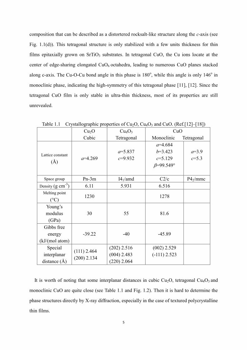
Table 1.1 Crystallographic properties of Cu2O, Cu4O3 and CuO. (Ref.[12]–[18])
Cu2O Cubic
Cu4O3
Tetragonal CuO
Monoclinic Tetragonal
Lattice constant
(Å) a=4.269
a=5.837 c=9.932
a=4.684 b=3.423 c=5.129 =99.549°
a=3.9 c=5.3
Space group Pn-3m I41/amd C2/c P42/mmc Density (g cm-3) 6.11 5.931 6.516
Melting point
(°C) 1230 1278
Young’s modulus
(GPa) 30 55 81.6
Gibbs free energy
(kJ/(mol atom) -39.22 -40 -45.89
Special interplanar
distance (Å)
(111) 2.464 (200) 2.134
(202) 2.516 (004) 2.483 (220) 2.064
(002) 2.529 (-111) 2.523
It is worth of noting that some interplanar distances in cubic Cu2O, tetragonal Cu4O3 and
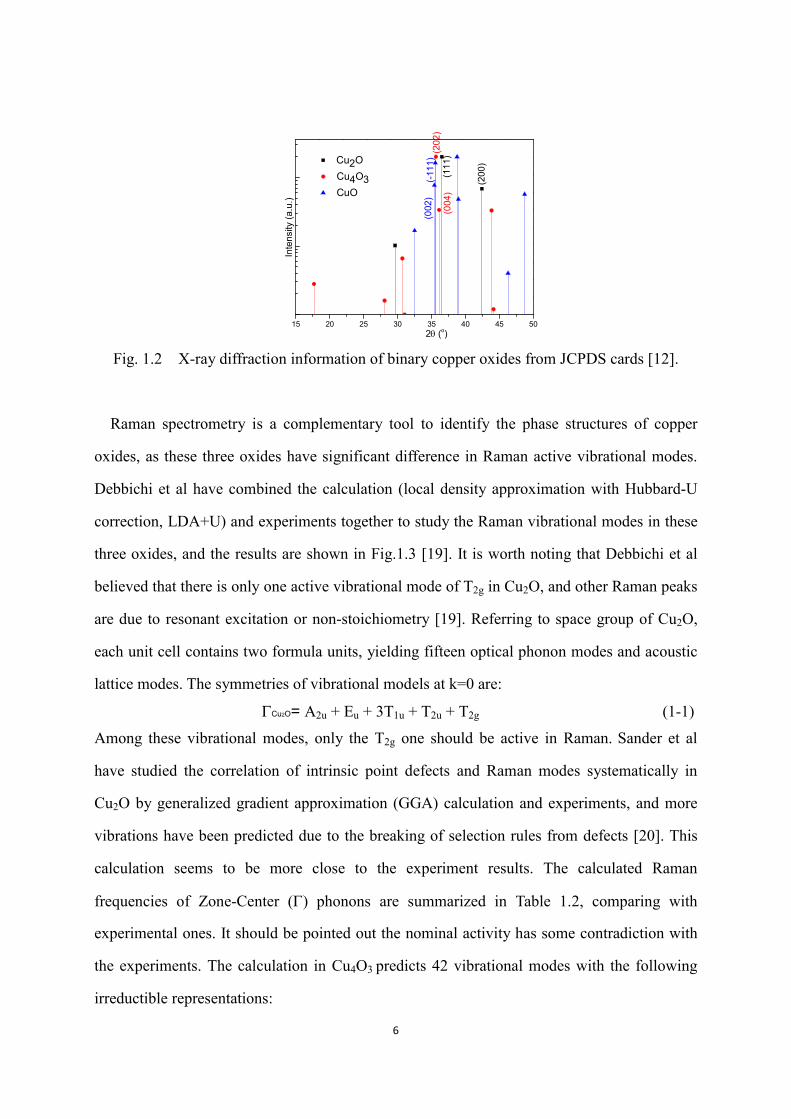
monoclinic CuO are quite close (see Table 1.1 and Fig. 1.2). Then it is hard to determine the
phase structures directly by X-ray diffraction, especially in the case of textured polycrystalline
thin films.
6
15 20 25 30 35 40 45 50
(-11
1)(0
02)
(004
)(2
02)
(200
)
(111
)
Inte
nsity
(a.u
.)
2(o)
Cu2O Cu4O3 CuO
Fig. 1.2 X-ray diffraction information of binary copper oxides from JCPDS cards [12].
Raman spectrometry is a complementary tool to identify the phase structures of copper
oxides, as these three oxides have significant difference in Raman active vibrational modes.
Debbichi et al have combined the calculation (local density approximation with Hubbard-U
correction, LDA+U) and experiments together to study the Raman vibrational modes in these
three oxides, and the results are shown in Fig.1.3 [19]. It is worth noting that Debbichi et al
believed that there is only one active vibrational mode of T2g in Cu2O, and other Raman peaks
are due to resonant excitation or non-stoichiometry [19]. Referring to space group of Cu2O,
each unit cell contains two formula units, yielding fifteen optical phonon modes and acoustic
lattice modes. The symmetries of vibrational models at k=0 are:
Cu2O= A2u + Eu + 3T1u + T2u + T2g (1-1)
Among these vibrational modes, only the T2g one should be active in Raman. Sander et al
have studied the correlation of intrinsic point defects and Raman modes systematically in
Cu2O by generalized gradient approximation (GGA) calculation and experiments, and more
vibrations have been predicted due to the breaking of selection rules from defects [20]. This
calculation seems to be more close to the experiment results. The calculated Raman
frequencies of Zone-Center () phonons are summarized in Table 1.2, comparing with
experimental ones. It should be pointed out the nominal activity has some contradiction with
the experiments. The calculation in Cu4O3 predicts 42 vibrational modes with the following
irreductible representations:
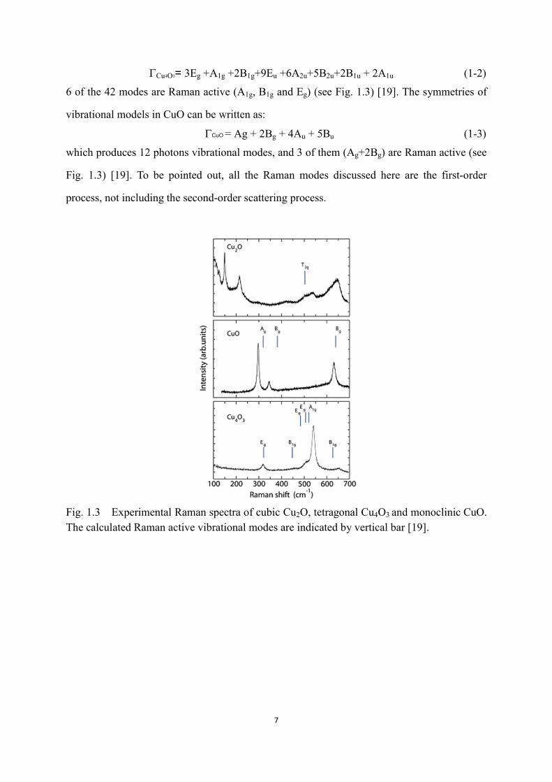
7
Cu4O3= 3Eg +A1g +2B1g+9Eu +6A2u+5B2u+2B1u + 2A1u (1-2)
6 of the 42 modes are Raman active (A1g, B1g and Eg) (see Fig. 1.3) [19]. The symmetries of
vibrational models in CuO can be written as:
CuO = Ag + 2Bg + 4Au + 5Bu (1-3)
which produces 12 photons vibrational modes, and 3 of them (Ag+2Bg) are Raman active (see
Fig. 1.3) [19]. To be pointed out, all the Raman modes discussed here are the first-order
process, not including the second-order scattering process.
Fig. 1.3 Experimental Raman spectra of cubic Cu2O, tetragonal Cu4O3 and monoclinic CuO. The calculated Raman active vibrational modes are indicated by vertical bar [19].

8
Table 1.2 Calculated (c) and experimental (e) Raman shift ((cm-1)) of Cu2O [20], [21], Cu4O3 [19], [22] and monoclinic CuO [19], [22].
Cu2O Cu4O3 CuO
Sym c e Sym c e Sym c e
T2u 71 86~100 Eg 321 311~318 Ag 319 286~296
Eu 84 108~110 Eg 506 505~510 Bg 382 333~346
T1u 147~148 147~152 A1g 521 531~541 Bg 639 619~631
A2u 338 308~350 B1g 627 643~651
T2g 499 487~520
T1u(TO) 608 609~635
T1u(LO) 630 650~665
1.2.2 Optical properties and band structures
1.2.2.1 Cu2O
Early experiments on excitons of Cu2O give a direct band gap of 2.17 eV at quite low
temperature [23]. Recently, the first principle calculations predict a direct band gap of about
1.97-2.1 eV and an optical band gap of about 2.5-2.7 eV [24]–[26], while the experimental
optical band gap is about 2.38-2.51 eV [27]. The band structure of Cu2O is shown in Fig.
1.4(a), where the energies of valence band maximum (VBM, ), the first conduction band
minimum (CBM, ) and the second CBM () are highlighted. The structure of Cu2O,
where the unit cell is rotated so that the O-Cu-O dumbbell motif is aligned along the z-axis is
depicted in Fig. 1.4(b). The VBM is mainly composed of Cu-d orbital and has even parity. At
the first CBM both the cation and the anion have contribution due to the O-Cu-O
dumbbell structure, but the intrasite s-d hybridization results in a strong Cu- 2zd contribution
to first CBMshowing the even parity. Then, the optical transition between VBM and first
CBM is dipole forbidden. However, the second CBM has a Cu- xyp character, with odd parity.
Hence, the optical transition between VBM and second CBM is allowed, and the value
corresponds to the optical band gap [24]. The experimental energy difference between the first

9
CBM and the second CBM is about 0.45 eV. Although different methods, such as
Heyd-Scuseria-Erzerhof (HSE), Green’s function calculations with screened Coulomb
interaction W (GW) and LDA+U, can well predict the band gap of about 2 eV, the conduction
band ordering between the first CBM and the second CBM exhibits striking difference.
Taking the G0W0RPA(HSE) as an example, a band gap of 1.91 eV is obtained (close to the
experimental 2.17 eV), but the energy difference between the first CBM and the second CBM
is – 0.38 eV, contradicting to the positive values in experiments [24]. Among the various
methods, HSE calculation has been demonstrated to be successful to describe the band gap
and band ordering, at the expense of high computational overhead.
Fig. 1.4 (a) The band structure of Cu2O. (b) The cuprite structure, shown so as to align the O-Cu-O dumbbell motif with the z-axis [24].
The computed density of states (DOSs) of Cu2O by HSE+G0W0 are shown in Fig. 1.5.
Comparing the full DOS with the partial DOS (PDOS), it is shown that the upper valence
band is mainly composed of Cu 3d character, while the lower valence band part is of
dominant O 2p character. There is a covalent mixing O 2p and Cu 3d, yielding a more
significant Cu 3d character in the upper valence band. The lower valence band part with O 2p
states also mixes with the Cu 3d states and enhances the O 2p character. .

10
Fig. 1.5 Full (a) and partial (b) DOSs of Cu2O calculated by by HSE+G0W0 [26].
1.2.2.2 Cu4O3
Although several groups have performed the first-principle calculation on band structure
[25], [28], and the experiments on optical properties [23], [24], [5], the properties of Cu4O3
are still full of debating. For instance, the theoretical calculations predicate an indirect band
gap of 0.78 eV by LDA+U [28]), and of 2.54 eV by HSE [25]. On the contrary, Ooi et al.
concluded a direct band gap of 2.2 eV by optical method [30]. Additionally, Pierson et al.
attained the experimental optical band gap of 1.34 eV or 2.47 eV, assuming either an indirect
or a direct band gap, respectively [29]. An indirect band gap of 1.25 eV was deduced from
linear augmented-plane-wave (LAPW) calculation [31].
Fig. 1.6 presents the electronic band dispersion of Cu4O3 calculated by LDA+U [28], which
clear shows the indirect band gap of 0.78 eV. The corresponding DOSs are depicted in Fig.
1.7. Looking into the details of DOS, the lower valence band is of dominant Cu1+/2+ 3d states,
and here strong O 2p and Cu 3d hybridization exists, yielding more significant Cu 3d
character. The upper valence band has O 2p character, accompanying with a hybridization.
Moving on to the conduction band, the DOS of Cu1+ is quite smaller than that of Cu2+, while
the energy difference between main Cu2+ and Cu1+ empty states is about 2 eV.

11
Fig. 1.6 Electronic band dispersion of Cu4O3 calculated by LDA+U [28].
Fig. 1.7 Full and partial densities of states in Cu4O3. Energy with respect to the Fermi level.Top panel: Total DOS obtained in the LDA (with non-magnetic ground state) and LDA+U (AF2 ground state). Lower panels: local spin-resolved DOSs on Cu2+, Cu1+ and O sites (average) in LDA+U. Positive (negative) values for spin-up (down) [28].
1.2.2.3 Monoclinic CuO
Even though monoclinic CuO has been widely studied for decades, there are still divergent
reports regarding its electronic and optical properties, due to its strong correlated interaction
among charge, spin, orbital and lattice. For instance, there is a contradiction in the type of
band gap: direct or indirect band gap. HSE and LDA+U calculations from Heinemann et al.

12
yield the indirect band gap of 2.74 and 1.39 eV, respectively [25]. Whereas, other articles
suggest a direct band gap of about 1.4 eV [5], [32], [33]. Moreover, the electronic structure of
CuO is still unambiguous, as the calculation electronic structure strongly depends on the
calculated methods or parameters [34]. For instance, different nonlocal Hartree-Fock
exchange α in HSE calculation will shift the states and change the band gaps, as shown in Fig.
1.9(a). Similar situations exist in Perdew-Burke-Ernzerhof with exchange correction
functional (PBE+U) calculation when tuning the U values (see Fig. 1.9(b)) [34].
Fig. 1.9 Orbital-projected DOS calculated with the hybrid functional for varying α (a) or with the PBE+U functional for varying U (b). The spin-up (positive values) and spin-down (negative values) contributions of the individual Cu 3d orbitals and the O 2p orbitals are shown. The VBM is set to zero and all DOS are convoluted with a Gaussian of 0.5 eV full width at half maximum (FWHM) [34].
1.2.2.4 Tetragonal CuO
Recently, the tetragonal CuO (also called elongated rocksalt structure) has drawn increasing
attention owing to its predicted high Néel temperature [10], [11], [17]. A recent experiment
gets a Néel temperature of 600 K [35]. Besides, Bednorz et al. have stated that oxides
containing transition metal ions with partially filled eg orbitals (such as Cu2+) will undergo
13
strong Jahn-Teller distortion and consequently can have strong electron-phonon interaction,
possibly giving rise to superconductivity [36]. The valence band spectra of tetragonal and
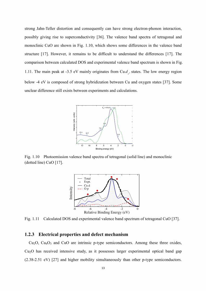
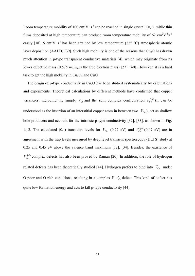
monoclinic CuO are shown in Fig. 1.10, which shows some differences in the valence band
structure [17]. However, it remains to be difficult to understand the differences [17]. The
comparison between calculated DOS and experimental valence band spectrum is shown in Fig.
1.11. The main peak at -3.5 eV mainly originates from Cu 2zd states. The low energy region
below -4 eV is composed of strong hybridization between Cu and oxygen states [37]. Some
unclear difference still exists between experiments and calculations.
Fig. 1.10 Photoemission valence band spectra of tetragonal (solid line) and monoclinic (dotted line) CuO [17].
Fig. 1.11 Calculated DOS and experimental valence band spectrum of tetragonal CuO [37].
1.2.3 Electrical properties and defect mechanism
Cu2O, Cu4O3 and CuO are intrinsic p-type semiconductors. Among these three oxides,
Cu2O has received intensive study, as it possesses larger experimental optical band gap
(2.38-2.51 eV) [27] and higher mobility simultaneously than other p-type semiconductors.
14
Room temperature mobility of 100 cm2V-1s-1 can be reached in single crystal Cu2O, while thin
films deposited at high temperature can produce room temperature mobility of 62 cm2V-1s-1
easily [38]. 5 cm2V-1s-1 has been attained by low temperature (225 oC) atmospheric atomic
layer deposition (AALD) [39]. Such high mobility is one of the reasons that Cu2O has drawn
much attention in p-type transparent conductive materials [4], which may originate from its
lower effective mass (0.575 mo, mo is the free electron mass) [27], [40]. However, it is a hard
task to get the high mobility in Cu4O3 and CuO.
The origin of p-type conductivity in Cu2O has been studied systematically by calculations
and experiments. Theoretical calculations by different methods have confirmed that copper
vacancies, including the simple CuV and the split complex configuration SplitCuV (it can be
understood as the insertion of an interstitial copper atom in between two CuV ), act as shallow
hole-producers and account for the intrinsic p-type conductivity [32], [33], as shown in Fig.
1.12. The calculated (0/-) transition levels for CuV (0.22 eV) and SplitCuV (0.47 eV) are in
agreement with the trap levels measured by deep level transient spectroscopy (DLTS) study at
0.25 and 0.45 eV above the valence band maximum [32], [34]. Besides, the existence of
SplitCuV complex defects has also been proved by Raman [20]. In addition, the role of hydrogen
related defects has been theoretically studied [44]. Hydrogen prefers to bind into CuV under
O-poor and O-rich conditions, resulting in a complex H- CuV defect. This kind of defect has
quite low formation energy and acts to kill p-type conductivity [44].

15
Fig. 1.12 Formation energy for intrinsic p-type defects in Cu2O in (a) Cu-rich (or O-poor) conditions and (b) Cu-poor (or O-rich) conditions. The dotted and the dashed lines indicate the positions of two traps from experiments [41].
The defect mechanism of CuO has been calculated preliminarily by LDA+U, which
predicts that CuV is the main defects to produce p-type conductivity [45], [46]. However, the
selection of Brillouin zone in Ref. [45] is thought to be questionable [8]. The defect
mechanism of Cu4O3 has not been reported.
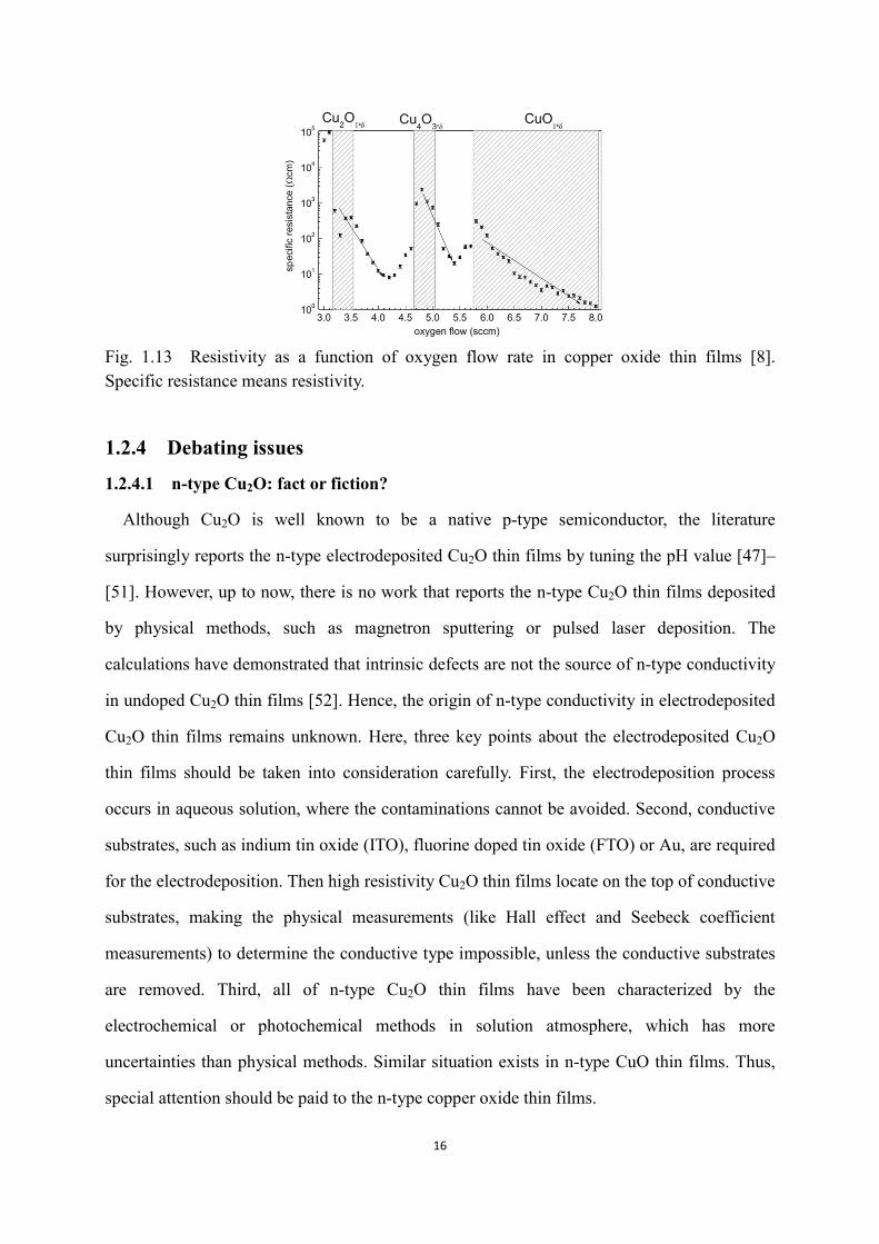
The evolution of room temperature resistivity as a function of oxygen flow rate in sputtered
copper oxide thin films is depicted in Fig. 1.13, where the shaded areas represent the single
phase synthesis window [8]. In these three single phase oxides, there is a similar tendency that
increasing the oxygen flow rate can decrease the resistivity. In Cu2O, this behavior can be
understood from the defect mechanism shown in Fig. 1.12. In oxygen rich conditions (high
oxygen flow rate), the formation energies for CuV and SplitCuV are lower, giving rise to higher
carrier concentration, consequently decreasing the resistivity. It is interesting to note that the
biphase thin films (Cu2O + Cu4O3 or Cu4O3 + CuO) have lower resistivity than single phase
films, as shown in Fig. 1.13. However, the Ref. [8] does not give a detailed explanation of this
experimental result.
16
Fig. 1.13 Resistivity as a function of oxygen flow rate in copper oxide thin films [8]. Specific resistance means resistivity.
1.2.4 Debating issues
1.2.4.1 n-type Cu2O: fact or fiction?
Although Cu2O is well known to be a native p-type semiconductor, the literature
surprisingly reports the n-type electrodeposited Cu2O thin films by tuning the pH value [47]–
[51]. However, up to now, there is no work that reports the n-type Cu2O thin films deposited
by physical methods, such as magnetron sputtering or pulsed laser deposition. The
calculations have demonstrated that intrinsic defects are not the source of n-type conductivity
in undoped Cu2O thin films [52]. Hence, the origin of n-type conductivity in electrodeposited
Cu2O thin films remains unknown. Here, three key points about the electrodeposited Cu2O
thin films should be taken into consideration carefully. First, the electrodeposition process
occurs in aqueous solution, where the contaminations cannot be avoided. Second, conductive
substrates, such as indium tin oxide (ITO), fluorine doped tin oxide (FTO) or Au, are required
for the electrodeposition. Then high resistivity Cu2O thin films locate on the top of conductive
substrates, making the physical measurements (like Hall effect and Seebeck coefficient
measurements) to determine the conductive type impossible, unless the conductive substrates
are removed. Third, all of n-type Cu2O thin films have been characterized by the
electrochemical or photochemical methods in solution atmosphere, which has more
uncertainties than physical methods. Similar situation exists in n-type CuO thin films. Thus,
special attention should be paid to the n-type copper oxide thin films.
17
1.2.4.2 Oxygen vacancy charge in Cu2O: positive or neutral?
Most of the photoluminescence (PL) spectra assume that oxygen vacancy OV is in positive
charge [8], [53]–[55]. However, recent theoretical results obtained by several groups using
different calculation methods tend to show that the oxygen vacancy in Cu2O is only stable in
the neutral state [42], [44], [56]. This also seems to mean that the assignments of defect peaks
in previous PL spectra should be reconsidered.
1.3 Synthesis methods
Till now, different kinds physical depositions (including magnetron sputtering (MS) and
pulsed laser deposition (PLD), chemical methods (such as chemical vapor deposition (CVD)
and atomic layer deposition (ALD)) and liquid phase synthesis (such as electrodepostion and
hydrothermal synthesis) have been widely used to grow copper oxide thin films. Here, we do
not want to present the details of different methods, but it is valuable to discuss their
advantages and disadvantages.
Physical deposition usually occurs in the vacuum atmosphere, whereas liquid phase
synthesis exists in solution with non-vacuum atmosphere. This means the low content of
H-related defects (acting as hole killer [44]) and other contaminations in films grown by
physical methods, which may yield higher carrier concentration in physical deposited thin
films. For instance, carrier concentration of 1016 - 1017 cm-3 in Cu2O has been attained by
magnetron sputtering with annealing treatment in the 200 - 300 oC temperature range [27]. In
contrast, electrodeposition only produces carrier concentration of 1013 - 1014 cm-3 with the
same kind of annealing treatment [57]. In addition, it is a hard task to synthesize pure phase
Cu4O3 by electrodeposition, as it is difficult to stabilize Cu2+ and Cu+ ions simultaneously via
conventional aqueous chemistry.
Chemical deposition processes, such as CVD and ALD, are also commonly used to grow
Cu2O and CuO thin films with large area, which requires special precursors. But these
precursors may introduce some contaminations [58], [59]. Besides, the synthesis of pure
phase Cu4O3 by chemical deposition is rarely reported.

18
High temperature is generally required to synthesize pure phase Cu2O by PLD [60], which
will block its wide applications. This high substrate temperature, together with the compound
target (like Cu2O and CuO ), will inhibit the growth of Cu4O3 by PLD.
Among the various thin film deposition technologies, reactive magnetron sputtering is a
good choice to grow binary copper oxides. It allows the selective deposition of the three
copper oxides, including Cu4O3 [23], [22], and it is also a very versatile technique for large
area deposition technique at low cost. It is worth pointing out that the non-equilibrium process
is required to grow single phase Cu4O3 thin films.
1.4 Recent progress of copper oxides based solar cells
1.4.1 Advantages of copper oxides
As the element abundance, non-toxicity, and easy fabrication, copper oxide based solar
cells are a promising class of photovoltaic (PV) devices with the characteristics of
being ¨ultra-low-cost¨ and of compatibility with terawatts-scale (TW) deployment. In 2009,
Wadia et al. have examined materials extraction costs and supply constraints for 23 promising
semiconductors, and copper oxides (Cu2O and CuO) are good candidates to meet the annual
worldwide electricity consumption of 17 000 TWh and much more lower cost than crystalline
silicon [61], as shown in Fig. 1.14. To be pointed out here, Schockley-Queisser limits of Cu2O
and CuO with sole consideration of band gaps are used to calculate these indexed results [62],
whereas other complicated physical properties (like optical absorption spectra and
radiative/nonradiative recombination processes) with strong influence on PV performance are
not taken into account, which gives rise to an overestimated index of CuO. In fact, the poor
electrical properties of CuO make the performance of present CuO based PV devices not as
good as Cu2O. Hence, here we just discuss the Cu2O-based heterojunction solar cells.

19
Fig. 1.14 Indexed results of 23 PV materials. The extraction costs, supply constraints and theoretical power conversion efficiency limit have been considered. All index values are divided by the calculated result of x-Si. The most attractive materials for large-scale future deployment are highlighted red and are in the upper right-hand quadrant [61].
1.4.2 Poor performance of Cu2O-based solar cells
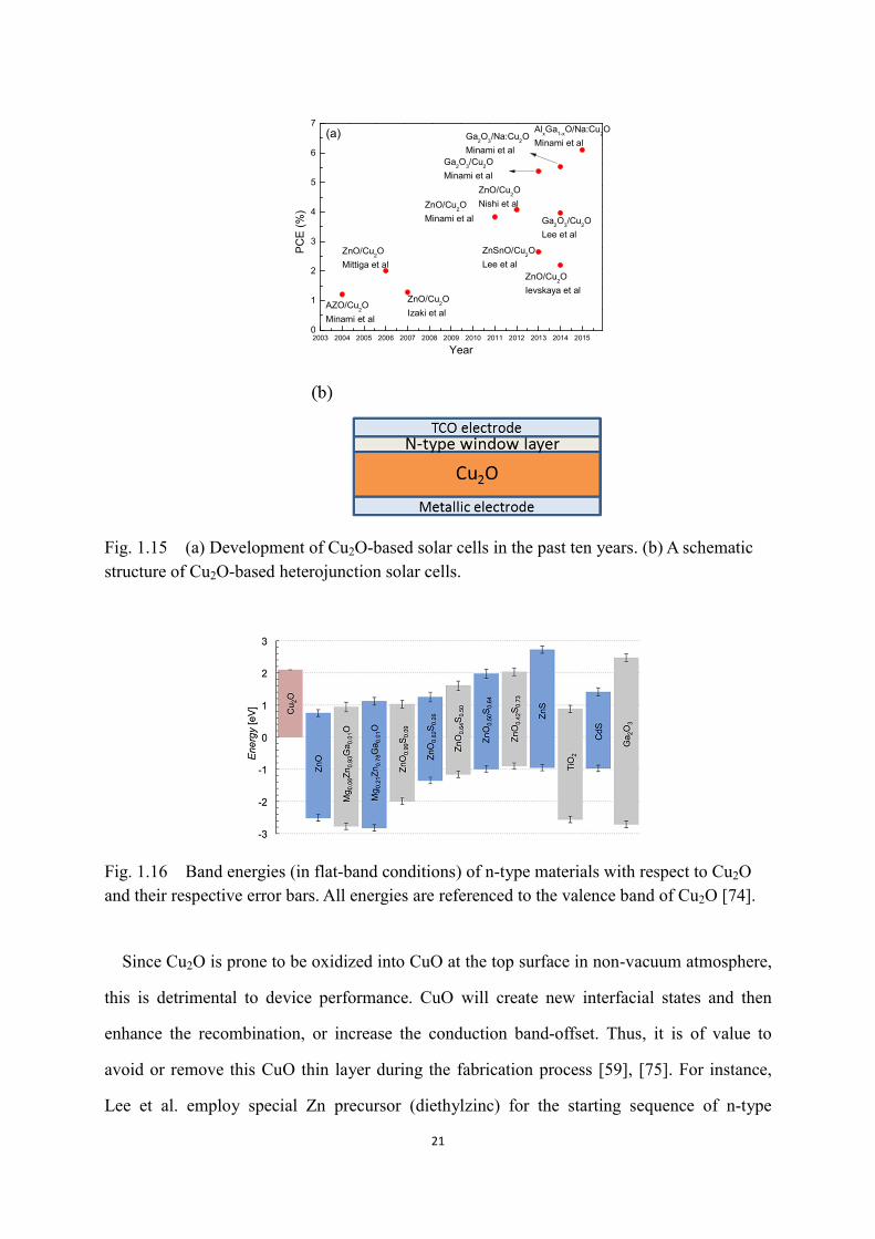
In the past ten years, Cu2O-based solar cells have experienced a great improvement [7],
[63]–[72] , as shown in Fig. 1.15(a). The conversion efficiency rises up from 1.21% in 2004
to 6.1% in 2015. The schematic structure of these solar cells is depicted in Fig. 15(b), where
n-type transparent semiconductors (such as ZnO, Zn1-xMgxO and Ga2O3) are usually used as
the window layer. However, the maximum experimental efficiency of 6.1% remains to be far
from its theoretical efficiency, and too poor to put into industry production. The origin of this
weak efficiency is still unclear, and several relevant issues are thought to be the possible
sources:
(a). Optical absorption of Cu2O
20% efficiency limit was roughly predicted by Schockley-Queisser theory [62], which only
considers the direct band gap of 2.17 eV measured at quite low temperature. In fact, Cu2O is a
dipole-forbidden direct band semiconductor, with an allowed transition optical band gap of

20
2.38-2.51 eV at room temperature [27]. The energy gap (∆) between minimal band gap ( gE )
and transition allowed band gap ( agE ) will increase the non-radiative recombination losses,
which plays negative roles in solar cells [73].
(b). Electrical properties of Cu2O
In order to get the large carrier transport lengths in the absorber, high mobility and low
density of defect are required to keep the high diffusion constants and large recombination
lifetime. In addition, low resistivity is also required to reduce the series resistance and the
contact resistance on the metal electrode. However, high density of defect is usually beneficial
to the high carrier concentration and low resistivity. Consequently, mobility and carrier
concentration compromise with each other in optimized conditions. Comparing most of the
publications in Cu2O-based heterojunction solar cells, it is found that Cu2O prepared by
thermal oxidizing at high temperature has higher efficiency () than other methods, which
may result from the high mobility from this high temperature oxidizing. More recently, the 6.1%
efficiency was achieved by the incorporation of sodium into the Cu2O sheets, which maintains
the high mobility and high carrier concentration simultaneously [7], [70].
(c). Conduction band offset between Cu2O and n-type layer
It is of great value that any potential ¨spike¨-type in the conduction band at the
heterojunction should be minimized for optimal minority carrier transport. Since the electron
affinity of Cu2O is as low as 3.2 eV, it is difficult to find a matched n-type partner exhibited so
low electron affinity. Brandt et al have surveyed band offset between Cu2O and a broad range
of n-type materials, as shown in Fig. 1.16, which provide fruitful information [74]. The
conduction band offset between Cu2O and ZnO is as high as -1.34 eV, which could be the
reason for its low open-circuit voltage. In contrast, a low offset of 0.38 eV was observed
between Cu2O and Ga2O3, which can explain its high performance to date. Besides, other
n-type materials, such as ternary alloys Zn(O,S) are thought to be potential candidates [74].
21
2003 2004 2005 2006 2007 2008 2009 2010 2011 2012 2013 2014 20150
1
2
3
4
5
6
7
PC
E (%
)
Year
AlxGa1-xO/Na:Cu2OMinami et al
ZnO/Cu2OIevskaya et al
Ga2O3/Cu2OLee et al
Ga2O3/Na:Cu2OMinami et al
ZnSnO/Cu2OLee et al
Ga2O3/Cu2OMinami et al
ZnO/Cu2ONishi et al ZnO/Cu2O
Minami et al
ZnO/Cu2OIzaki et al
ZnO/Cu2OMittiga et al
AZO/Cu2OMinami et al
(a)
Fig. 1.15 (a) Development of Cu2O-based solar cells in the past ten years. (b) A schematic structure of Cu2O-based heterojunction solar cells.
Fig. 1.16 Band energies (in flat-band conditions) of n-type materials with respect to Cu2O and their respective error bars. All energies are referenced to the valence band of Cu2O [74].
Since Cu2O is prone to be oxidized into CuO at the top surface in non-vacuum atmosphere,
this is detrimental to device performance. CuO will create new interfacial states and then
enhance the recombination, or increase the conduction band-offset. Thus, it is of value to
avoid or remove this CuO thin layer during the fabrication process [59], [75]. For instance,
Lee et al. employ special Zn precursor (diethylzinc) for the starting sequence of n-type
22
amorphous zinc-tin-oxide window layer to reduce the CuO surface layer to Cu2O by forming
ZnO, yielding the efficiency of 2.85% [59]. In some extremal conditions, Cu2O will be
decomposed into Cu, which also should be averted.
1.5 Chapter conclusions
In this chapter, a general review of binary copper oxides focusing on their structural,
electronic structure, optical and electrical properties, as well as the recent developments of
copper oxide based solar cells has been presented. Basic needs include systematical
investigations on controllable growth and characterization of Cu2O, Cu4O3 and CuO thin
films. There is a clear demand to understand the unusual properties, such as lower resistivity
in biphase thin films, from the viewpoint of microstructure. Moreover, a joint experimental
and theoretical study is required to understand their optical properties, valence and conduction
band structures. Experimental optical absorption can be used to study the optical properties,
while photoemission and electron energy loss spectroscopies are required to determine the
band structure. Combining these experimental results with theoretical calculations, may yield
a better understanding on their electronic structures, which may also provide a way to
evaluate the calculation methods.

23
Chapter 2 Experimental and calculational details
2.1 Introduction
In this thesis, reactive magnetron sputtering has been used to synthesize the copper oxide
and nickel oxide thin films. X-ray diffraction, Raman spectrometry, scanning electron
microscopy (SEM) and transmission electron microscopy (TEM) have been employed to
study the structure and the microstructure of the films. The electrical properties have been
studied using the four point probe method and the Hall effect measurements. The electronic
structures have been investigated by X-ray photoemission spectroscopy (XPS), ultraviolet
photoemission spectroscopy (UPS) and electron energy loss spectroscopy (EELS). In addition,
many-body perturbation theory in the GW approximation has been used to calculate the
electronic structures and optical properties. In this chapter, an introduction of some of these
experimental and theoretical methods will be presented.
2.2 Thin film growth
Reactive magnetron sputtering is one of the many so-called PVD techniques. In this
process, target material is sputtered in the presence of a gas mixture such as argon-oxygen to
deposit an oxide. The main role of argon is to sputter the metallic target while oxygen atoms
react at the film surface with the metallic atoms to form the oxide. Then, the composition of
the film is strongly influenced by the amount of reactive gas introduced into the deposition
chamber. Nowadays reactive magnetron sputtering is a widely used for industrial coating
deposition as well as for scientific research.
Fig. 2.1 shows the schematic view of the reactive sputtering chamber. The thin film growth
process can be described like this:
- cleaning the substrates by ethanol;
- installing the substrates on the holder and switching on the pumping to the base
vacuum (approx. 10-3 - 10-4 Pa);

24
- introducing Ar to etch the substrate surface using a radiofrequency plasma
- introducing oxygen and switching on the pulsed-DC plasma on the target and
switching off the etching plasma.
Fig. 2.1 Schematic drawing of reactive sputtering chamber. The black, red and green circles represent Ar, Cu and O, respectively.
All the copper oxide thin films in this thesis were deposited on glass (microscopy slides)
and (100) silicon substrates by magnetron sputtering in various Ar-O2 reactive mixtures.
During the deposition, no intentional heating was applied to the substrates, and the deposition
temperature was close to room temperature. The argon flow rate was fixed at 25 standard
cubic centimeter per minute (sccm), while the oxygen flow rate varied in the 7-30 sccm range.
Thin films were deposited at different total sputtering pressure (0.5, 1 and 2 Pa) by changing
the pumping speed via a throttle valve. A pulsed-DC supply (Pinnacle+ Advanced Energy)
was used to sputter the copper target (50 mm diameter and 3 mm thick with a purity of
99.99 %, Ampere Industry). The current applied to target was fixed to 0.3 A, the frequency
and the off-time were 50 kHz and 4 µs, respectively. The distance between the substrate and
the target was fixed at 60 mm. To be pointed out here, the target voltage and the oxygen
partial pressure as a function of the oxygen flow rate have been recorded, in order to find the
critical oxygen flow rate to synthesize the oxide thin films. However, the hysteresis effect is
not observed neither in the target voltage nor in the oxygen partial pressure, making a
difficulty to determine the elemental sputtering mode (ESM) and the reactive sputtering mode

25
(RSM). Such a behavior may be due to the low gettering effect of copper atoms, to the low
wall area of our sputtering chamber and to the high pumping speed [76]–[78]. The thickness
of copper oxide thin films deposited during 10 minutes is shown in Fig. 2.2. Taking the 0.5 Pa
total sputtering pressure as an example, when the oxygen flow rate is between 12 and 20 sccm,
the growth rate is quite close. The thickness decreases when the oxygen flow rate exceeds 20
sccm. Since the increase of the total pressure reduces the mean free path of sputtered copper
atoms, a smaller amount of copper atoms attends the substrate surface and the film thickness
is lower than that measured at 0.5 Pa. Meanwhile, a smaller amount of oxygen is required to
oxidize the copper atoms when the total pressure is fixed at 1 Pa.
. 10 12 14 16 18 20 22 24
0
200
400
600
800
1000
Film
thic
knes
s (n
m)
Oxygen flow rate (sccm)
Total pressure: 0,5 Pa Total pressure: 1 Pa
Fig. 2.2 Evolution of the copper oxide thin film thickness as a function of the oxygen flow rate using two values of total pressures. Whatever the oxygen flow rate or the total pressure, the deposition duration was 10 minutes.
Nickel oxide thin films have been also deposited using the same sputtering chamber. The
deposition procedure for NiO films is similar to that used for copper oxide ones. For NiO thin
film deposition, no intentional heating was applied to the substrate holder. The argon flow rate
was fixed at 25 sccm, while the oxygen flow rate varied in the 4-11 sccm range, with the total
pressure of about 0.5 Pa. A pulsed-DC supply (Pinnacle+ Advanced Energy) was connected to
the metallic nickel target (2 in. diameter and 1 mm thick with a purity of 99.995%). The
current applied to the target, the frequency and the off-time were fixed to 0.3 A, 50 kHz and 4
µs, respectively. The distance between the substrate and the target was fixed at 75 mm. The
26
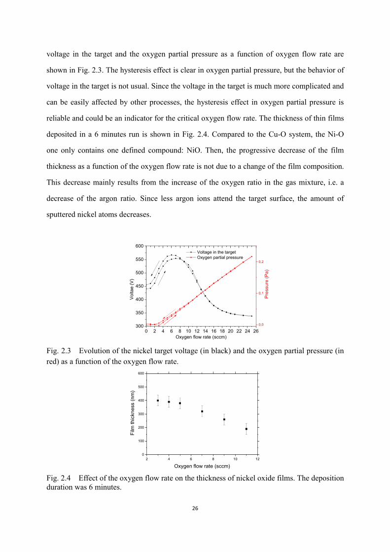
voltage in the target and the oxygen partial pressure as a function of oxygen flow rate are
shown in Fig. 2.3. The hysteresis effect is clear in oxygen partial pressure, but the behavior of
voltage in the target is not usual. Since the voltage in the target is much more complicated and
can be easily affected by other processes, the hysteresis effect in oxygen partial pressure is
reliable and could be an indicator for the critical oxygen flow rate. The thickness of thin films
deposited in a 6 minutes run is shown in Fig. 2.4. Compared to the Cu-O system, the Ni-O
one only contains one defined compound: NiO. Then, the progressive decrease of the film
thickness as a function of the oxygen flow rate is not due to a change of the film composition.
This decrease mainly results from the increase of the oxygen ratio in the gas mixture, i.e. a
decrease of the argon ratio. Since less argon ions attend the target surface, the amount of
sputtered nickel atoms decreases.
0 2 4 6 8 10 12 14 16 18 20 22 24 26300
350
400
450
500
550
600 Voltage in the target Oxygen partial pressure
Oxygen flow rate (sccm)
Volta
e (V
)
0,0
0,1
0,2 P
ress
ure
(Pa)
Fig. 2.3 Evolution of the nickel target voltage (in black) and the oxygen partial pressure (in red) as a function of the oxygen flow rate.
2 4 6 8 10 120
100
200
300
400
500
600
Film
thic
knes
s (n
m)
Oxygen flow rate (sccm) Fig. 2.4 Effect of the oxygen flow rate on the thickness of nickel oxide films. The deposition duration was 6 minutes.

27
2.3 Thin film characterization
2.3.1 X-ray diffraction
X-ray diffraction (XRD) relies on the dual wave/particle nature of X-rays to obtain the
information of crystalline materials, including crystallographic structure, orientation, strain
state, and so on. When an incident X-ray beam interacts with a material, the dominant effect is
scattering of X-rays from atoms constituting the material. In crystalline materials, the
scattered X-rays undergo constructive and destructive interference. This method of X-ray
diffraction can be described by Bragg’s law, as shown in Fig. 2.5. A set of crystallographic
lattice planes with distances dhkl is irradiated by plane wave x-rays impinging on the lattice
planes at an angle θ. The relative phase shift of the wave depends on the configuration of
atoms as is seen for the two darker atoms in the top plane and one plane beneath. The phase
shift comprises of two shares, Δ1 and Δ2, the sum of which equals 2dsinθ for any arbitrary
angle θ. Constructive interference for the reflected wave, however, can only be achieved when
the phase shift is a multiple of the wavelength [79].
Fig. 2.5 Visualization of the Bragg equation. Maximum scattered intensity is only observed when the phase shifts add to amultiple of the incident wavelength [79].
In this thesis, the structure and growth orientation of thin films were checked by XRD
(Brucker D8 Advance with CuKα1 radiation ( = 0.15406 nm)) in Bragg Brentano
configuration. The determination of the structure was performed using the JCPDS data and
the EVA software provided by Brucker. Pole figures were obtained using a Brucker D8
Discover diffractometer (Co K radiation, = 0.17912 nm).
28
2.3.2 Raman spectrometry
Raman spectrometry is commonly used in materials science, since vibrational information
is specific to the chemical bonds and crystallographic symmetry. Therefore, it provides a
fingerprint by which the material can be identified. The Raman scattered light occurs at
wavelengths that are shifted from the incident light by the energies of molecular vibrations.
The mechanism of Raman scattering is different from that of infrared absorption, and Raman
and IR spectra provide complementary information [80].
Here, micro-Raman spectrometry (Horiba LabRAM HR using a 532 nm laser) was
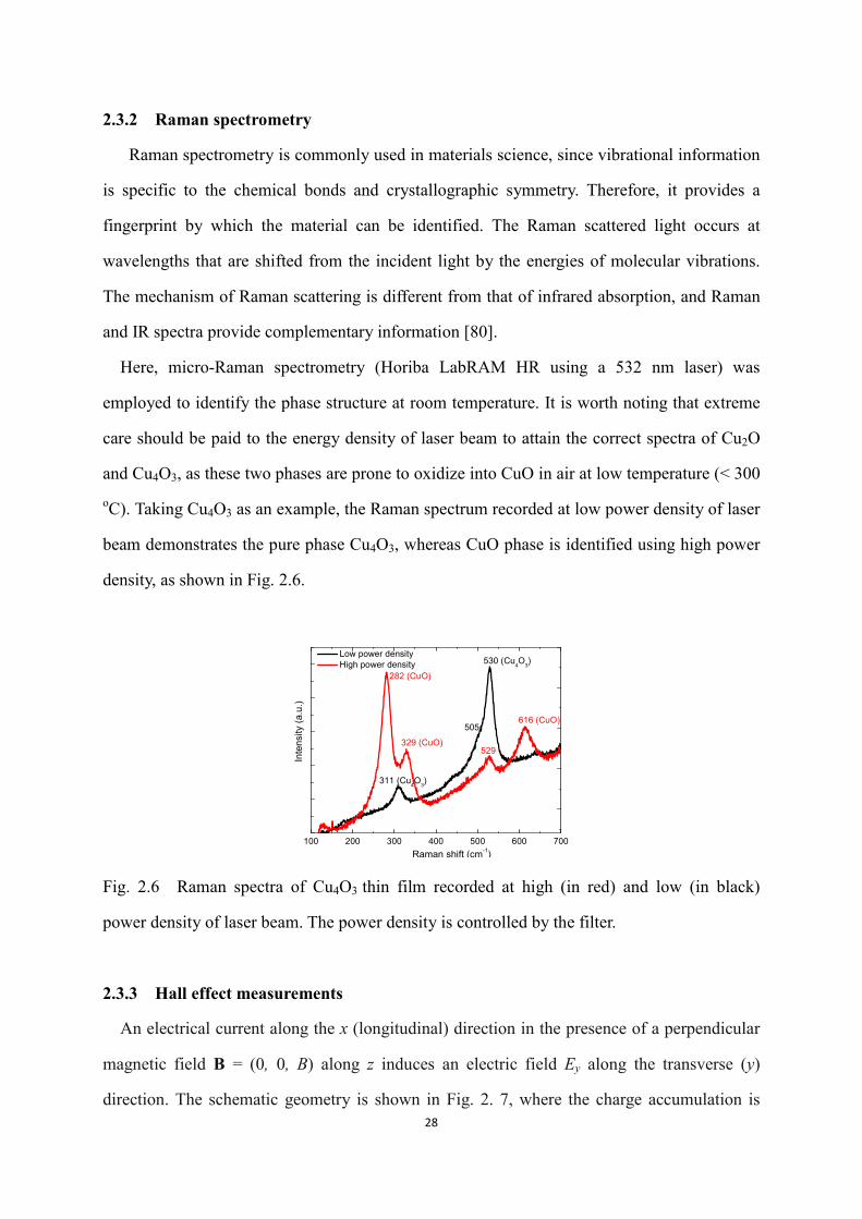
employed to identify the phase structure at room temperature. It is worth noting that extreme
care should be paid to the energy density of laser beam to attain the correct spectra of Cu2O
and Cu4O3, as these two phases are prone to oxidize into CuO in air at low temperature (< 300 oC). Taking Cu4O3 as an example, the Raman spectrum recorded at low power density of laser
beam demonstrates the pure phase Cu4O3, whereas CuO phase is identified using high power
density, as shown in Fig. 2.6.
100 200 300 400 500 600 700
Low power density High power density
Raman shift (cm-1)
Inte
nsity
(a.u
.)
616 (CuO)
529329 (CuO)
530 (Cu4O3)
505
311 (Cu4O3)
282 (CuO)
Fig. 2.6 Raman spectra of Cu4O3 thin film recorded at high (in red) and low (in black)
power density of laser beam. The power density is controlled by the filter.
2.3.3 Hall effect measurements
An electrical current along the x (longitudinal) direction in the presence of a perpendicular
magnetic field B = (0, 0, B) along z induces an electric field Ey along the transverse (y)
direction. The schematic geometry is shown in Fig. 2. 7, where the charge accumulation is

29
due to the Lorentz force. The related transverse voltage is called the Hall voltage (VH), which
can be described as
nteIBVH (2-1)
where I is the current across the plate length, B is the magnetic field, t is the thickness of the
plate, e is the elementary charge, and n is the charge carrier density of the carrier electrons
[81]. The Hall effect measurements can determine accurately conductive type (p or n type),
carrier density, electrical resistivity, and the mobility of carriers in semiconductors.
Fig. 2.7 Scheme of the Hall-effect geometry [81].
In this thesis, the electrical properties were measured using a Hall measurement system in
the van der Pauw geometry (Ecopia, HMS-5000) with a DC magnetic field of 0.57 T. To be
pointed out, since we grow thin films at room temperature, the carrier concentration and
mobility of as-deposited Cu2O thin films cannot be measured correctly as the mobility is out
of our detecting limit. After air annealing, this could be solved. However, in the cases of
Cu4O3 and CuO thin films, the mobility is still too low to determine correctly even with air
annealing thermal treatments. Then Seebeck coefficient measurement is employed to identify
the conductive type in Cu4O3 and CuO thin films.
2.3.4 Transmission electron microscopy
TEM is a microscopy technique in which a beam of electrons is transmitted through an
ultra-thin specimen, interacting with the specimen as it passes through. Then an image is
formed from the interaction of the electrons transmitted through the specimen. TEM has
revolutionized our understanding of materials by completing the
processing-structure-properties links down to atomistic levels. It is now possible to tailor the
30
microstructure of materials to achieve specific sets of properties; the extraordinary abilities of
modern TEM to provide almost all the structural, microstructural, and chemical information
[82].
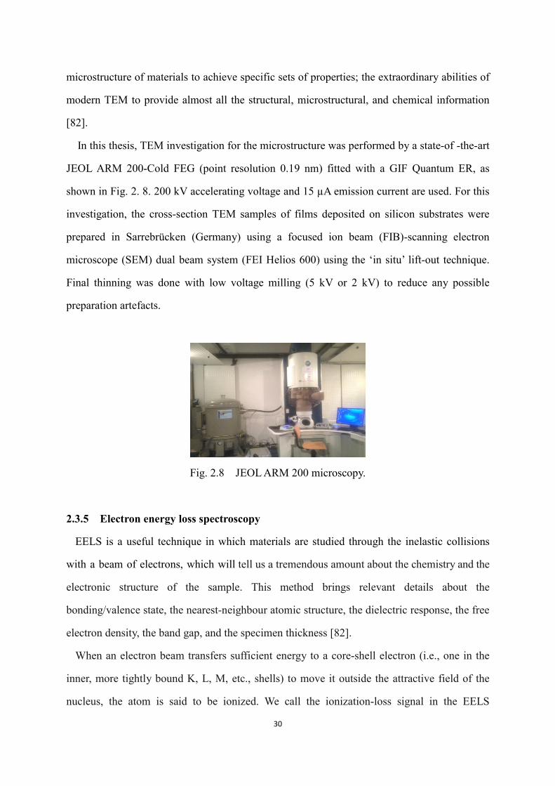
In this thesis, TEM investigation for the microstructure was performed by a state-of -the-art
JEOL ARM 200-Cold FEG (point resolution 0.19 nm) fitted with a GIF Quantum ER, as
shown in Fig. 2. 8. 200 kV accelerating voltage and 15 µA emission current are used. For this
investigation, the cross-section TEM samples of films deposited on silicon substrates were
prepared in Sarrebrücken (Germany) using a focused ion beam (FIB)-scanning electron
microscope (SEM) dual beam system (FEI Helios 600) using the ‘in situ’ lift-out technique.
Final thinning was done with low voltage milling (5 kV or 2 kV) to reduce any possible
preparation artefacts.
Fig. 2.8 JEOL ARM 200 microscopy.
2.3.5 Electron energy loss spectroscopy
EELS is a useful technique in which materials are studied through the inelastic collisions
with a beam of electrons, which will tell us a tremendous amount about the chemistry and the
electronic structure of the sample. This method brings relevant details about the
bonding/valence state, the nearest-neighbour atomic structure, the dielectric response, the free
electron density, the band gap, and the specimen thickness [82].
When an electron beam transfers sufficient energy to a core-shell electron (i.e., one in the
inner, more tightly bound K, L, M, etc., shells) to move it outside the attractive field of the
nucleus, the atom is said to be ionized. We call the ionization-loss signal in the EELS

31
spectrum an ‘edge,’ rather than a peak. The K shell electron is in the 1 s state and gives rise to
a single K edge. In the L shell, the electrons are in either 2s or 2p orbitals. If a 2s electron is
ejected, we get an L1 edge, and 2p1/2 or 2p3/2 electrons causes L2 or L3 edges, respectively. The
variation in intensity, extending several tens of eV above the ionization edge onset (Ec), is the
energy loss near edge structure (ELNES), also called as fine structure, which effectively
mirrors the unfilled DOS above Fermi level, as shown in Fig. 2.9. White lines are the most
important part in ELNES, which are intense sharp peaks on certain ionization edges. These
sharp peaks arise because in certain elements the core electrons are excited into well-defined
empty states, not a broad continuum. Due to the dipole-selection rule, in the case of the p state,
the only permitted final states are either a s state or a d state. Consequently, the core electrons
are ejected primarily into the unoccupied d states in the conduction band, since there are few
available s states. Thus, L2, 3 white lines means the existence d shell with unfilled states [82].
Fig. 2.9 Relationship between the empty DOS and the ELNES intensity in the ionization edge fine structure [82].
For the ELNES spectra measurements here, the accelerating voltage of 200 kV, the
emission current of 5 uA and the energy dispersion of 0.05 eV/ch were used. All the spectra
were acquired in the diffraction mode, with the energy resolution of 0.45~0.5 eV defined by
the full width at half maximum (FWHM) of the zero loss peak (ZLP). The convergence
semi-angle and the collection semi-angle were 7 and 18 mrad, respectively. Here the
suitable acquisition time and number of frame should be chosen to record the correct ELNES

32
spectra of Cu2O thin films, as long time irradiation from the electron beam has a tendency to
oxidize Cu2O into CuO, even in the vacuum (10-5 Pa) atmosphere.
Low acceleration voltage (80 kV) and low emission current (2 uA) are employed to avoid
the relativistic effect, especially the Cerenkov radiation, and to get a FWHM of ZLP with the
value of 0.3~0.35 eV in the valence EELS (VEELS) measurements.
2.3.6 Photoemission spectroscopy
Photoemission spectroscopy is based on the principle of photoelectric effect: photons from
a light source are absorbed by the sample surface and induce the emission of electrons. There
are two types of photoemission spectroscopy, categorized by light source: XPS (X-ray to
examine core levels) and UPS (UV radiation to study the valence band)
XPS spectra are obtained by irradiating a material with a X-ray beam and simultaneously
measuring the kinetic energy and number of electrons that escape from the top layer of a few
nanometers of the material surfaces. XPS detects all elements with an atomic number (Z) of 3
(lithium) and above. XPS has similar function with EELS in chemical analysis, such as
valence state, composition determination. But significant differences exist in the thickness
analysed and the so-called chemical shift. XPS is surface sensitive with a penetration depth of
a few nanometers, while electron beam passes through the sample with the thickness up to
150 nm (depending on the acceleration voltage) in EELS spectrometer equipped in a TEM. In
XPS, the kinetic energies of photoelectrons that escape into the surrounding vacuum are
measured by an electron spectrometer. So, the final state of the electron transition lies in a
continuum far above the vacuum level and is practically independent of the specimen. In the
case of a compound, any increase in binding energy of a core level, relative to its value in the
pure (solid) element, is called a chemical shift. The ionization-edge threshold energies observed
in EELS represent a difference in energy between the core-level initial state and the lowest
energy final state of the excited electron. The corresponding chemical shifts in threshold energy
are more complicated than in XPS because the lowest energy final state lies below the vacuum
level and its energy depends on the valence-electron configuration [83].

33
UPS is analogous to XPS but the excitation source is a helium discharge source. The
photon energy can be optimized for He I = 21.2 eV or He II = 44.8 eV which is significantly
lower energy than Al (1486.7 eV) or Mg Kα (1253.6 eV) used in XPS. As with XPS the
binding energy (EBE) is related to the measured photoelectron kinetic energy (EK) by the
simple Einstein’s photoelectric law. This kind of lower photon energy will result in that only
the low binding energy valence electrons may be excited by the He source. A further
consequence of the low photon energy is UPS is more surface sensitive than XPS and thus
very sensitive to surface contamination.
All the XPS/UPS spectra were measured in a UHV chamber. The Ar+ ion etching was
performed again and again to clean the surface, until there is no evolution in the C-1s XPS
spectra. The XPS source was a monochromatic Al K line, while the ultraviolet photon
source was He I. The silver paste was put in a corner of the sample, contacting with the
metallic holder. The purpose of this is to relieve the charge effect during the measurement and
to identify the Fermi level by using silver as a reference.
2.4 Theoretical calculation method
Many-body perturbation theory in the GW approximation has emerged as a standard
computational tool for the band structure prediction of semiconductors and insulators,
providing a systematic improvement of band structures calculated in the local-density or
generalized gradient approximations (LDA or GGA) to density functional theory (DFT). The
past decade has seen considerable developments in GW method with different schemes.
However, there is presently no single universally accepted scheme for GW calculations, which
can fairly describe both band gaps and band structures of semiconductors, especially the
transition metal oxides. In this work, a GW scheme with the consideration of local-field effect
and an empirical on-site potential for transition metal d orbitals with a single parameter per
transition metal cation (noted as GWLF + Vd), has been used, which allows for reasonably
predictive band gaps for different oxide stoichiometries and TM oxidation states at an
acceptable computational expense [24].

34
The calculations are performed within the projector augmented wave (PAW) implementation
of the VASP code (version 5.2). With the goal of a feasible scheme for high-throughput
band-structure prediction in mind, computationally expedient PAW data sets were chosen for
the present study: For oxygen, a “soft” potential was used, allowing for a relative small energy
cutoff for the wave functions of 320 eV. All the calculations in this manuscript are done by Dr
Stephane Lany from National Renewable Energy Laboratory in USA.
2.5 Chapter conclusions
In this chapter, the experimental and calculational details, including the thin film deposition
parameters, thin film characterization methods, theoretical calculation approach and some
important technical issues concerning on the characterizations have been presented. These
different methods will be used in the next chapters to reveal the properties of copper oxide
thin films.
35
Chapter 3 Tuning the structure and preferred orientation in
reactively sputtered copper oxide thin films
3.1 Introduction
For scientific research or technological applications, it is of great interest to fabricate binary
copper oxide thin films with high quality. Up to now, most of the usual deposition methods
have been used to grow Cu2O and CuO thin films, including magnetron sputtering [29], [31],
molecular beam epitaxy [84], pulsed laser deposition [60], and electrochemical deposition
[57]. Since it is difficult to stabilize Cu2+ and Cu+ ions simultaneously via conventional
aqueous chemistry, it is hard to synthesize pure Cu4O3 by electrochemical deposition and
sol-gel methods. The synthesis of pure Cu2O phase by pulsed laser deposition or molecular
beam epitaxy usually requires high temperature that limits its wide applications [60], [84].
Among the various thin film deposition technologies, reactive magnetron sputtering is a good
choice to grow binary copper oxides, as it allows the selective deposition of the three copper
oxides, including Cu4O3 [29], [31] . This process is also a highly versatile technique for large
area deposition at low cost.
The crystal growth orientation of thin films has great impact on the microstructure and
properties of films. Thus, it is interesting to grow copper oxide thin films with tunable
preferred orientation. Several parameters may be used to control the film growth in magnetron
sputtering processes such as oxygen partial pressure, total pressure, substrate orientation,
substrate temperature, and the use of a buffer or seed layer [21], [85]–[87]. Although
lattice-matched substrates and high substrate temperature have typically been employed to
tune the growth orientation, the harsh conditions are undesirable for large scale applications at
low cost. Hence, controlling the growth orientation at room temperature using conventional
substrates with random orientation will extend the application range of copper oxide thin
films.
In this chapter, we have investigated the selective growth of the three copper oxide thin
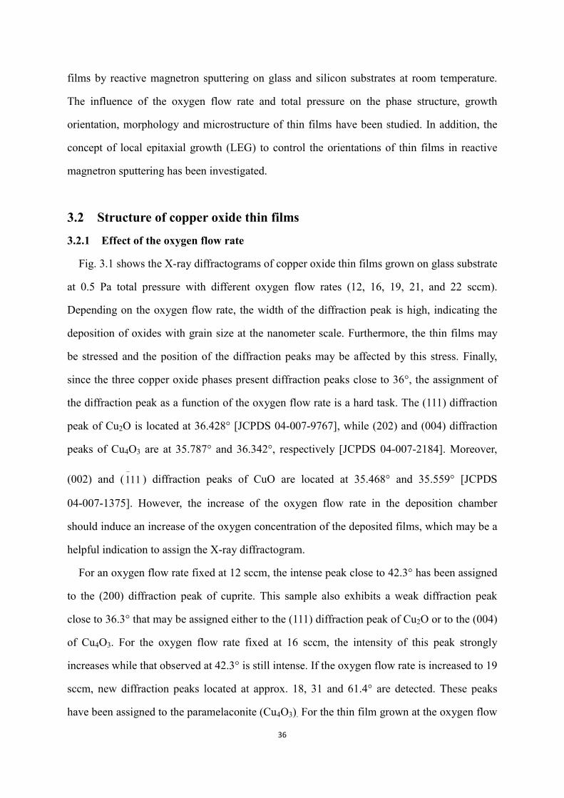
36
films by reactive magnetron sputtering on glass and silicon substrates at room temperature.
The influence of the oxygen flow rate and total pressure on the phase structure, growth
orientation, morphology and microstructure of thin films have been studied. In addition, the
concept of local epitaxial growth (LEG) to control the orientations of thin films in reactive
magnetron sputtering has been investigated.
3.2 Structure of copper oxide thin films
3.2.1 Effect of the oxygen flow rate
Fig. 3.1 shows the X-ray diffractograms of copper oxide thin films grown on glass substrate
at 0.5 Pa total pressure with different oxygen flow rates (12, 16, 19, 21, and 22 sccm).
Depending on the oxygen flow rate, the width of the diffraction peak is high, indicating the
deposition of oxides with grain size at the nanometer scale. Furthermore, the thin films may
be stressed and the position of the diffraction peaks may be affected by this stress. Finally,
since the three copper oxide phases present diffraction peaks close to 36°, the assignment of
the diffraction peak as a function of the oxygen flow rate is a hard task. The (111) diffraction
peak of Cu2O is located at 36.428° [JCPDS 04-007-9767], while (202) and (004) diffraction
peaks of Cu4O3 are at 35.787° and 36.342°, respectively [JCPDS 04-007-2184]. Moreover,
(002) and ( 111
) diffraction peaks of CuO are located at 35.468° and 35.559° [JCPDS
04-007-1375]. However, the increase of the oxygen flow rate in the deposition chamber
should induce an increase of the oxygen concentration of the deposited films, which may be a
helpful indication to assign the X-ray diffractogram.
For an oxygen flow rate fixed at 12 sccm, the intense peak close to 42.3° has been assigned
to the (200) diffraction peak of cuprite. This sample also exhibits a weak diffraction peak
close to 36.3° that may be assigned either to the (111) diffraction peak of Cu2O or to the (004)
of Cu4O3. For the oxygen flow rate fixed at 16 sccm, the intensity of this peak strongly
increases while that observed at 42.3° is still intense. If the oxygen flow rate is increased to 19
sccm, new diffraction peaks located at approx. 18, 31 and 61.4° are detected. These peaks
have been assigned to the paramelaconite (Cu4O3). For the thin film grown at the oxygen flow

37
rate of 21 sccm, the X-ray diffractogram shows an X-ray amorphous material (see Fig. 3.1(b)).
Hence, it seems that the use of XRD as the only characterization method is not relevant to
clearly distinguish the phase structures in these binary copper oxide polycrystal thin films.
Fig. 3.1 (a) X-ray diffractograms of copper oxide thin films deposited at 0.5 Pa total pressure with 12, 16, 19, 21, and 22 sccm oxygen flow rate. (b) Magnified diffractogram of thin film deposited with 21 sccm O2.
Since Cu2O, Cu4O3 and CuO have different Raman active vibrational modes [19], Raman
spectrometry is a good complementary method to determine the film phase structure. Fig. 3.2
shows the Raman spectra of the copper oxide thin films previously characterized by XRD in
Fig. 3.1. For films deposited at 19 sccm of oxygen, the Eg (311 and 505 cm-1) and A1g (531
cm-1) Raman bands of Cu4O3 are clearly evidenced. This result is in agreement with that from
XRD, indicating the use of 19 sccm in our deposition conditions leads to the synthesis of pure
paramelaconite thin films. These two Raman bands are also evidenced for the films deposited
at 16 sccm oxygen, accompanied by some new bands at approx. 93, 147 and 216 cm-1 that
have been ascribed to special modes in Cu2O [20], [88]. This demonstrates the deposition of a
mixture of Cu2O and Cu4O3. Since the Raman bands of paramelaconite are not detected in the
film deposited at 12 sccm anymore, this sample only contains the Cu2O phase and the weak
diffraction peak close to 36.3° is related to the Cu2O (111) diffraction peak (Fig. 3.1(a)).
Moreover, when the oxygen flow rate is increased to 21 sccm, Raman analysis shows besides
the A1g band of Cu4O3, the existence of a new band close to 288 cm-1 that corresponds to the
CuO phase. Hence, this indicates the 21 sccm oxygen flow rate results in the deposition of an

38
X-ray amorphous mixture of Cu4O3 and CuO. Finally, when the oxygen flow rate is fixed at
22 sccm, the Raman bands of Cu4O3 disappear and only those of CuO are evidenced. In
summary, increasing the oxygen flow rate induces the progressive oxidation of the sputtered
copper atoms. Combining XRD and Raman analyses, it has been shown that pure Cu2O,
Cu4O3 or CuO can be deposited. Between these single phase domains, biphase materials can
be synthesized (Cu2O + Cu4O3 or Cu4O3 + CuO). These results are in agreement with those
previously published by Meyer et al. although their Raman spectrum of Cu4O3 is questionable
[8].
Fig. 3.2 Raman spectra of copper oxide thin films deposited at 0.5 Pa total pressure with 12, 16, 19, 21 and 22 sccm oxygen flow rate.
3.2.2 Effect of the total pressure
The combination of XRD and Raman analyses has also been used to determine the phases
present in films deposited at higher pressure of 1 and 2 Pa as a function of the oxygen flow

39
rate by a step of 1 sccm. Fig. 3.3 shows the schematic deposition diagram of binary copper
oxide thin films, which roughly describes the phase structure as the function of oxygen flow
rate and total pressure. As detailed in Fig. 3.1 and 3.2, the increase of the oxygen flow rate at
a given total pressure induces the evolution from single phase Cu2O, biphase Cu2O and Cu4O3,
single phase Cu4O3, biphase Cu4O3 and CuO, and finally single phase CuO. It is observed that
the O2 flow rate process windows to synthesize single phase Cu2O and Cu4O3 are narrow
(about 2 or 3 sccm). In contrast, the process window for single phase CuO is wider. As seen in
Fig. 3.3, with the increase of total pressure, the oxygen flow rate window for single phase
deposition has a tendency to become narrower. Additionally, the single phase deposition
domains are shifted to lower oxygen flow rate value, which can be understood considering
that the increase of the total pressure reduces the mean free path of sputtered copper atoms
and lowers the film deposition rate. Consequently less oxygen is required to get the expected
phase. The change of the total pressure induces an increase of the oxygen partial pressure that
may affect the structure of the deposited films. Then, the previous deposition diagram has
been also plotted using the oxygen partial pressure instead of the total pressure (not shown
here) but this diagram does not give relevant information to explain the evolution of the film
structure as a function of the oxygen flow rate at various total pressures. At 0.5 Pa total
pressure, the oxygen partial pressure required to deposit pure paramelaconite is about
0.16-0.17 Pa while that required to deposit Cu4O3 at 2 Pa is about 0.37 Pa.
Finally, it should be pointed out that some films deposited at 2 Pa exhibit cracks at the top
surface resulting from tensile stress and their electrical resistivity is extremely high. This
means that high total pressure is not suitable for depositing binary copper oxide thin films of
good physical quality. Since the films deposited at 2 Pa show poor functional properties, this
deposition conditions will not further be considered in this thesis.
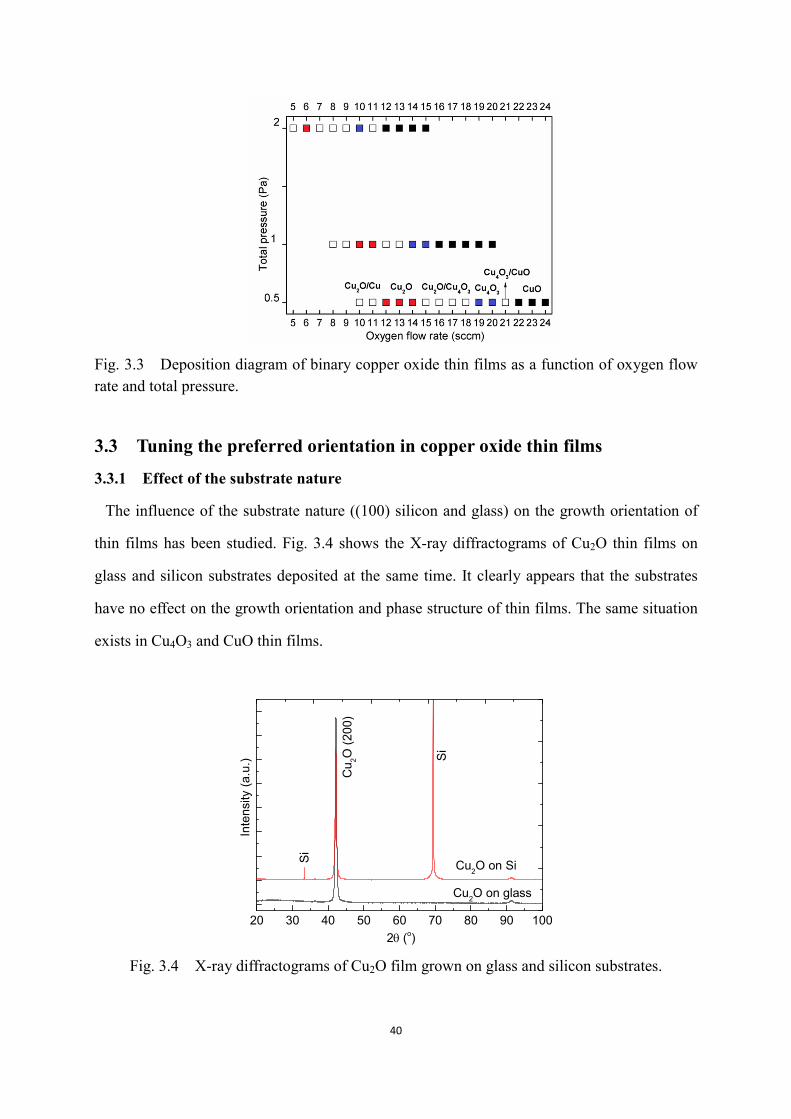
40
Fig. 3.3 Deposition diagram of binary copper oxide thin films as a function of oxygen flow rate and total pressure.
3.3 Tuning the preferred orientation in copper oxide thin films
3.3.1 Effect of the substrate nature
The influence of the substrate nature ((100) silicon and glass) on the growth orientation of
thin films has been studied. Fig. 3.4 shows the X-ray diffractograms of Cu2O thin films on
glass and silicon substrates deposited at the same time. It clearly appears that the substrates
have no effect on the growth orientation and phase structure of thin films. The same situation
exists in Cu4O3 and CuO thin films.
20 30 40 50 60 70 80 90 100
Cu 2O
(200
)
Si
Si
Cu2O on Si
Inte
nsity
(a.u
.)
2(o)
Cu2O on glass
Fig. 3.4 X-ray diffractograms of Cu2O film grown on glass and silicon substrates.

41
3.3.2 Preferred orientation of Cu2O thin films
Since the oxygen flow rate process window for single phase Cu2O deposition is narrow, the
influence of this parameter on the growth orientation is quite limited (see Fig. 3.5). However,
the total pressure has a significant effect on the film preferred orientation. As shown in Fig.
3.6(a), only the (200) diffraction peak of cuprite deposited at the total pressure of 0.5 Pa is
clearly observed by XRD, indicating a texture along the <100> orientation. The increase of
the total pressure to 1 Pa strongly modifies the X-ray diffractogram and only the (111)
diffraction peak is clearly evidenced. Here, it is worth noting that the tunable texture of Cu2O
does not change the sign of the internal stress. Using the Stoney’s method, <100> and <111>
oriented Cu2O thin films exhibit the compressive stress of 290 ± 10 MPa and 80 ± 20 MPa,
respectively. Top-view SEM images of Cu2O thin films deposited at 0.5 Pa and 1 Pa are
shown in Fig. 3.6(b) and 3.6(c), respectively, which demonstrates that the grain size of film
deposited at 0.5 Pa (approx. in the 20-35 nm range) is larger than that deposited at 1 Pa
(approx. in the 10-25 nm range).
20 30 40 50 60 70 80 90
Cu 2O
(111
) Cu 2O
(200
)
Inte
nsity
(a.u
.)
2(o)
0.5 Pa-12 sccm O2
0.5 Pa-13 sccm O2
0.5 Pa-14 sccm O2
(a)
20 30 40 50 60 70 80 90
Cu 2O
(111
)
Inte
nsity
(a.u
.)
2(o)
1 Pa-10 sccm 1 Pa-11 sccm
(b)
Fig. 3.5 X-ray diffractograms of single phase Cu2O thin films deposited at 0.5 Pa (a) and 1 Pa (b) with different oxygen flow rates.
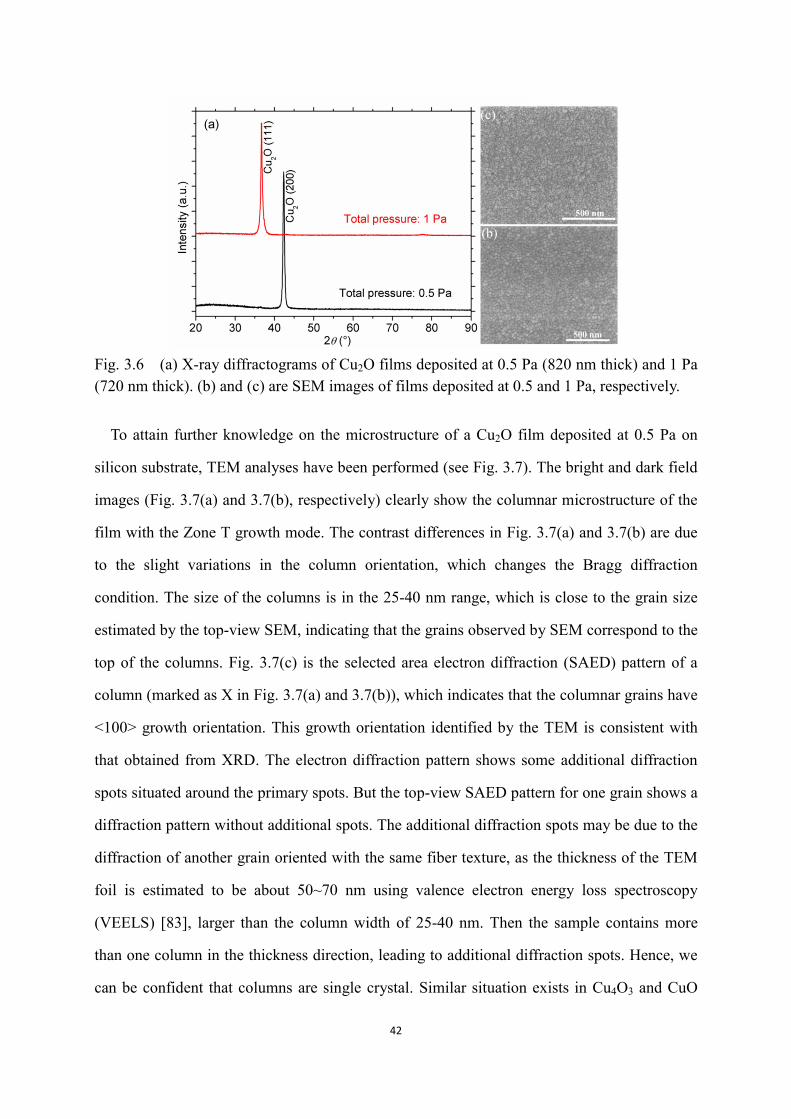
42
Fig. 3.6 (a) X-ray diffractograms of Cu2O films deposited at 0.5 Pa (820 nm thick) and 1 Pa (720 nm thick). (b) and (c) are SEM images of films deposited at 0.5 and 1 Pa, respectively.
To attain further knowledge on the microstructure of a Cu2O film deposited at 0.5 Pa on
silicon substrate, TEM analyses have been performed (see Fig. 3.7). The bright and dark field
images (Fig. 3.7(a) and 3.7(b), respectively) clearly show the columnar microstructure of the
film with the Zone T growth mode. The contrast differences in Fig. 3.7(a) and 3.7(b) are due
to the slight variations in the column orientation, which changes the Bragg diffraction
condition. The size of the columns is in the 25-40 nm range, which is close to the grain size
estimated by the top-view SEM, indicating that the grains observed by SEM correspond to the
top of the columns. Fig. 3.7(c) is the selected area electron diffraction (SAED) pattern of a
column (marked as X in Fig. 3.7(a) and 3.7(b)), which indicates that the columnar grains have
<100> growth orientation. This growth orientation identified by the TEM is consistent with
that obtained from XRD. The electron diffraction pattern shows some additional diffraction
spots situated around the primary spots. But the top-view SAED pattern for one grain shows a
diffraction pattern without additional spots. The additional diffraction spots may be due to the
diffraction of another grain oriented with the same fiber texture, as the thickness of the TEM
foil is estimated to be about 50~70 nm using valence electron energy loss spectroscopy
(VEELS) [83], larger than the column width of 25-40 nm. Then the sample contains more
than one column in the thickness direction, leading to additional diffraction spots. Hence, we
can be confident that columns are single crystal. Similar situation exists in Cu4O3 and CuO

43
thin films. The high resolution TEM (HRTEM) image (as seen in Fig. 3.7(d)), shows an
interplanar distance of ~0.21 nm, corresponding to the (200) planes of Cu2O.
Fig. 3.7 TEM micrographies of single phase Cu2O thin film deposited at 0.5 Pa. (a) Bright field image. (b) Dark field image. (c) Electron diffraction pattern of a column (marked as X in (a) and (b)). (d) HRTEM image.
3.3.3 Preferred orientation of Cu4O3 thin films
Akin to the case of Cu2O, the oxygen flow rate has quite limit influence on the growth
orientation. The preferred orientation of single phase Cu4O3 thin films is also strongly
dependent on the total pressure: <101> orientated film is grown at 0.5 Pa total pressure while
<100> preferred orientation is obtained at 1 Pa (see Fig. 3.8(a)). Fig. 3.8(b) and 3.8(c) are the
top-view SEM images of single phase Cu4O3 thin films deposited at 0.5 Pa and 1 Pa,
respectively. When the total pressure is fixed at 0.5 Pa, most of the grains exhibit a roof-type
morphology due to the [101] preferred orientation in this tetragonal structure (Fig. 3.8(b)). On
the other hand, the surface morphology of films deposited at 1 Pa can be depicted as
elongated grains (Fig. 3.8(c)).
TEM micrographies of Cu4O3 thin films deposited at 0.5 Pa are shown in Fig. 3.9. The film
also grows with a columnar microstructure and the column width has been estimated in the
30-70 nm range, as shown in Fig. 3.9(a) and 3.9(b). This large range comes from the
distribution of in-plane grain orientation. The electron diffraction pattern of a column (marked
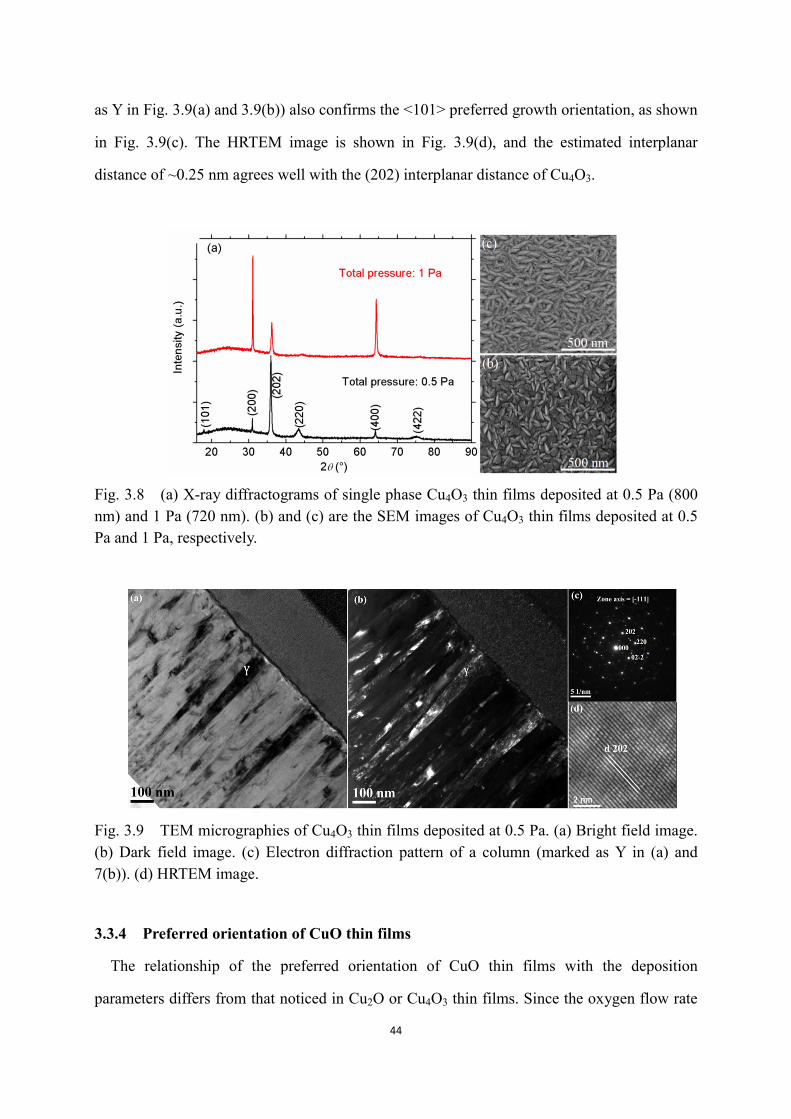
44
as Y in Fig. 3.9(a) and 3.9(b)) also confirms the <101> preferred growth orientation, as shown
in Fig. 3.9(c). The HRTEM image is shown in Fig. 3.9(d), and the estimated interplanar
distance of ~0.25 nm agrees well with the (202) interplanar distance of Cu4O3.
Fig. 3.8 (a) X-ray diffractograms of single phase Cu4O3 thin films deposited at 0.5 Pa (800 nm) and 1 Pa (720 nm). (b) and (c) are the SEM images of Cu4O3 thin films deposited at 0.5 Pa and 1 Pa, respectively.
Fig. 3.9 TEM micrographies of Cu4O3 thin films deposited at 0.5 Pa. (a) Bright field image. (b) Dark field image. (c) Electron diffraction pattern of a column (marked as Y in (a) and 7(b)). (d) HRTEM image.
3.3.4 Preferred orientation of CuO thin films
The relationship of the preferred orientation of CuO thin films with the deposition
parameters differs from that noticed in Cu2O or Cu4O3 thin films. Since the oxygen flow rate

45
process window to synthesize single phase CuO thin films is wide (see Fig. 3.3), the oxygen
flow rate may play a dominant role on the preferred orientation of CuO thin films. Fig. 3.10
shows the X-ray diffractograms and SEM images of CuO thin films deposited at 1 Pa for 10
min with different oxygen flow rates. It is worth noting that the thin films deposited at 0.5 Pa
have the similar evolution of growth orientation. Referring to the JCPDS 04-007-1375 with a
Cu Kα1 radiation, the CuO diffraction peaks of (002) (2°) and ( )111 (2°),
(111) (2°) and (200) (2°) are close, so it is hard to index the diffraction
peaks at about ° and 38° in Fig. 10(a) from this Bragg Brentano configuration. The sum of
X-ray diffractograms of CuO films (1 Pa total pressure and 24 sccm oxygen flow rate)
obtained at different angles (tilt angle on a Eulerian 4-circle diffractometer) from a Co K
radiation shows that the diffraction peak at about 38° is not symmetrical (see Fig. 3.11), which
indicates that both (111) and (200) diffraction planes contribute to this peak and (111) plane
plays the predominant role. The SEM image of CuO thin films deposited with 16 sccm O2
(see Fig. 3.10(b)) shows that most of the grains have a pyramidal shape, which confirms that
the <111> orientation could be the main growth orientation. This observation is also in
agreement with first-principle calculations that demonstrate the surface energy of {111}
planes (0.74 J/m2) is much lower than that in polar {100} planes (2.28 J/m2) [89]. In the case
of the diffraction peak at about 35° in Fig. 3.10(a) measured by Cu Kα1 radiation, the
diffractograms from Co K radiation with different angles depicted in Fig. 3.11 still can not
identify the diffraction planes, as (002) and ( 111
) diffraction peaks are too close to be
distinguished by XRD. Since the {001} planes contain alternating planes of Cu2+ and O2-,
they are also expected to be polar surfaces with electrostatical instability and high surface
energy, similar with {100} planes. Then the ( 111
) planes with second lower surface energy
(0.86 J/m2) [89], may play the main contribution to the diffraction peak at about 35° in Fig.
3.10(a). Hence, it is clearly shown in Fig. 3.10 that low O2 flow rate leads to the formation of
<111> preferred orientation, while high O2 flow rate results in the < 111
> texture. Here it
should be noted that the stress of CuO thin films is still low. For instance, CuO thin films
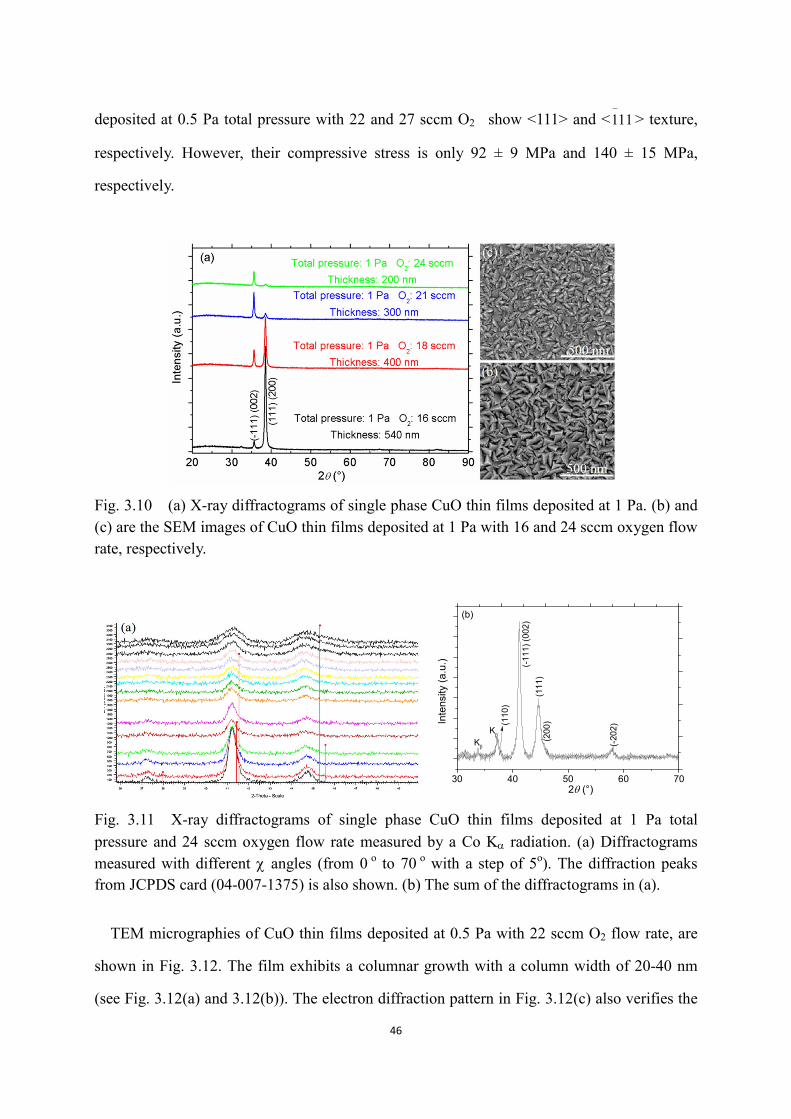
46
deposited at 0.5 Pa total pressure with 22 and 27 sccm O2 show <111> and < 111
> texture,
respectively. However, their compressive stress is only 92 ± 9 MPa and 140 ± 15 MPa,
respectively.
Fig. 3.10 (a) X-ray diffractograms of single phase CuO thin films deposited at 1 Pa. (b) and (c) are the SEM images of CuO thin films deposited at 1 Pa with 16 and 24 sccm oxygen flow rate, respectively.
30 40 50 60 70
(200
)
(-20
2)
(111
) (-
111)
(002
)
(110
)
K
Inte
nsity
(a.u
.)
2 (°)
K
(b)
Fig. 3.11 X-ray diffractograms of single phase CuO thin films deposited at 1 Pa total pressure and 24 sccm oxygen flow rate measured by a Co K radiation. (a) Diffractograms measured with different angles (from 0 o to 70 o with a step of 5o). The diffraction peaks from JCPDS card (04-007-1375) is also shown. (b) The sum of the diffractograms in (a).
TEM micrographies of CuO thin films deposited at 0.5 Pa with 22 sccm O2 flow rate, are
shown in Fig. 3.12. The film exhibits a columnar growth with a column width of 20-40 nm
(see Fig. 3.12(a) and 3.12(b)). The electron diffraction pattern in Fig. 3.12(c) also verifies the

47
<111> growth orientation. The interplanar distance measured from the HRTEM image in Fig.
3.12(d) is about 0.23 nm and this value agrees well with that of (111) planes.
Fig. 3.12 TEM micrographies of CuO thin films deposited at 0.5 Pa with 22 sccm O2. (a) Bright field image. (b) Dark field image. (c) Electron diffraction pattern of a column (marked as Z in Fig. 9(a) and 9(b)). (d) HRTEM image.
3.3.5 Discussion about the preferred orientation in copper oxide thin films
The evolution of thin film growth orientation is typically affected by the substrate
temperature, substrate orientation, surface energy of materials, growth mode, growth rate,
energetic particle bombardment, surface diffusion [85]–[87], [90]–[92]. All these factors
interact with each other and form a complex system. However, here we are able to grow
binary copper oxide thin films with tunable growth orientation on amorphous substrates (glass)
or single crystal substrate (silicon) at room temperature. Taking Cu2O as an example, both
theoretical calculations and experiments have demonstrated that the surface energy (V) of
different planes evolves in the order V(100) > V(110) > V(111) [93], [94], which means the (111)
plane is the most stable. Therefore, it is deemed that low total pressure allows to produce the
high surface energy of {100} planes parallel to the substrate, and high total pressure enables
to form the low surface energy of {111} planes parallel to the substrate. In the case of Cu4O3,
the atomic density has been calculated due to no reported data about the surface energy, which
shows the {101} planes have fewer atomic density than {100} ones. Provided that the
principle (planes with larger atomic density have smaller surface energy) exists in Cu4O3,
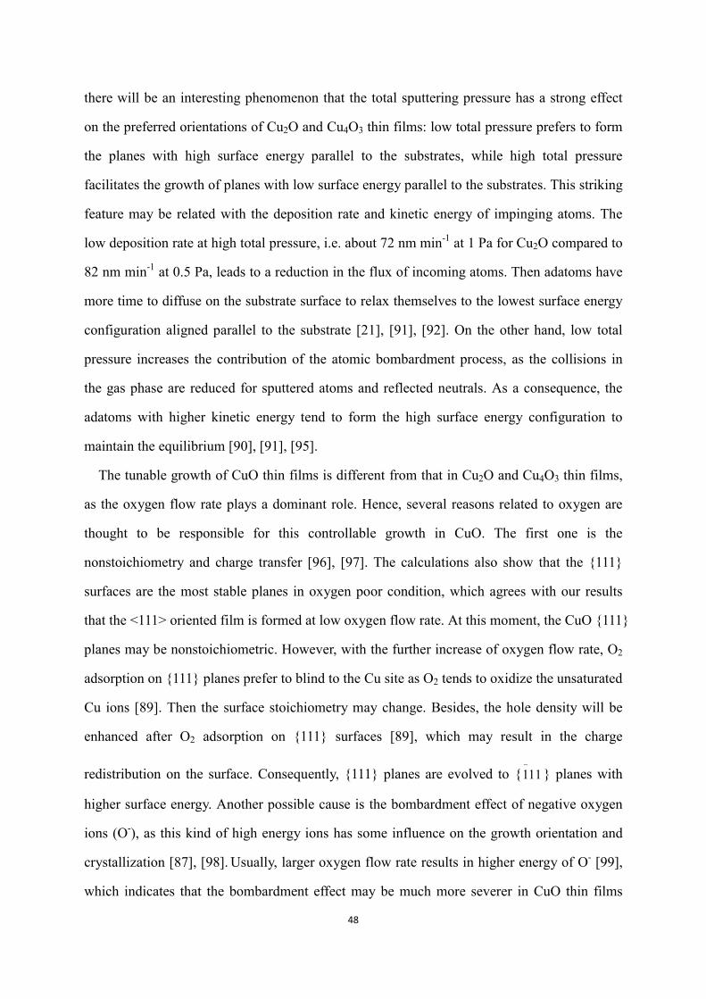
48
there will be an interesting phenomenon that the total sputtering pressure has a strong effect
on the preferred orientations of Cu2O and Cu4O3 thin films: low total pressure prefers to form
the planes with high surface energy parallel to the substrates, while high total pressure
facilitates the growth of planes with low surface energy parallel to the substrates. This striking
feature may be related with the deposition rate and kinetic energy of impinging atoms. The
low deposition rate at high total pressure, i.e. about 72 nm min-1 at 1 Pa for Cu2O compared to
82 nm min-1 at 0.5 Pa, leads to a reduction in the flux of incoming atoms. Then adatoms have
more time to diffuse on the substrate surface to relax themselves to the lowest surface energy
configuration aligned parallel to the substrate [21], [91], [92]. On the other hand, low total
pressure increases the contribution of the atomic bombardment process, as the collisions in
the gas phase are reduced for sputtered atoms and reflected neutrals. As a consequence, the
adatoms with higher kinetic energy tend to form the high surface energy configuration to
maintain the equilibrium [90], [91], [95].
The tunable growth of CuO thin films is different from that in Cu2O and Cu4O3 thin films,
as the oxygen flow rate plays a dominant role. Hence, several reasons related to oxygen are
thought to be responsible for this controllable growth in CuO. The first one is the
nonstoichiometry and charge transfer [96], [97]. The calculations also show that the {111}
surfaces are the most stable planes in oxygen poor condition, which agrees with our results
that the <111> oriented film is formed at low oxygen flow rate. At this moment, the CuO {111}
planes may be nonstoichiometric. However, with the further increase of oxygen flow rate, O2
adsorption on {111} planes prefer to blind to the Cu site as O2 tends to oxidize the unsaturated
Cu ions [89]. Then the surface stoichiometry may change. Besides, the hole density will be
enhanced after O2 adsorption on {111} surfaces [89], which may result in the charge
redistribution on the surface. Consequently, {111} planes are evolved to { 111
} planes with
higher surface energy. Another possible cause is the bombardment effect of negative oxygen
ions (O-), as this kind of high energy ions has some influence on the growth orientation and
crystallization [87], [98]. Usually, larger oxygen flow rate results in higher energy of O- [99],
which indicates that the bombardment effect may be much more severer in CuO thin films

49
with large oxygen flow rate, leading to the evolution of growth orientation. Further
experimental and theoretical investigations are required to clarify the mechanism.
3.4 Evidence of a local homoepitaxial growth mechanism in copper oxide
thin films
3.4.1 Study of Cu2O thin films
As previously reported, for a total sputtering pressure of 0.5 Pa and an oxygen flow rate of
13 sccm, a single diffraction peak belonging to the (100) planes of Cu2O is found which
indicates a texture along the <100> direction, as seen in Fig. 3.13. In the following this
deposition conditions will be referred as “Cu2O (I)”. In contrast, the films exhibit a <111>
texture for conditions corresponding to a total sputtering pressure of 1 Pa and an oxygen flow
rate of 11 sccm. In the following this deposition conditions will be referred as “Cu2O (II)”. In
both cases, the full width at half maximum (FWHM) of the diffraction peaks are larger than
the instrumental one indicating a nanocrystalline character. Moreover, the diffraction peaks
position leads for Cu2O (I) and (II) to a cubic lattice parameter a = 0.4288 and 0.4263 nm,
respectively. Since the lattice constant of bulk Cu2O is 0.427 nm, the measured values may
result from the composition shift in Cu2O (I) and (II) layers. Here it should be pointed out that
the oxygen flow rate process window for pure Cu2O synthesis is narrow (approx. 3 sccm for
0.5 Pa total sputtering pressure and approx. 2 sccm for 1 Pa total sputtering pressure), as seen
in Fig. 3.3. Within this process window, the oxygen flow rate has almost no influence on the
texture of Cu2O thin films. Fig. 3.13(b) and 3.13(c) show the (200) plane pole figure of Cu2O
(I) and (111) plane pole figure of Cu2O (II), respectively. The pole figures for others planes,
i.e. (111) for Cu2O (I) and (200) for Cu2O (II), have also been measured, but no preferred
orientation (not shown here) has been evidenced perpendicularly to these planes. These results
confirm the single layer Cu2O thin films present a fiber texture that can be set along the <100>
or <111> directions. The FWHM of the rocking curve measured along [200] and [111]
directions for Cu2O (I) and (II) are equal to 10.6° and 10.5°, respectively, indicating a similar
mosaicity for both deposition conditions.
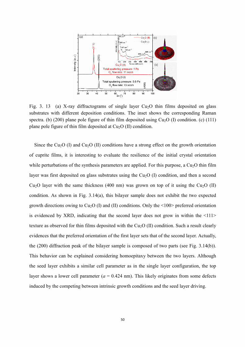
50
Fig. 3. 13 (a) X-ray diffractograms of single layer Cu2O thin films deposited on glass substrates with different deposition conditions. The inset shows the corresponding Raman spectra. (b) (200) plane pole figure of thin film deposited using Cu2O (I) condition. (c) (111) plane pole figure of thin film deposited at Cu2O (II) condition.
Since the Cu2O (I) and Cu2O (II) conditions have a strong effect on the growth orientation
of cuprite films, it is interesting to evaluate the resilience of the initial crystal orientation
while perturbations of the synthesis parameters are applied. For this purpose, a Cu2O thin film
layer was first deposited on glass substrates using the Cu2O (I) condition, and then a second
Cu2O layer with the same thickness (400 nm) was grown on top of it using the Cu2O (II)
condition. As shown in Fig. 3.14(a), this bilayer sample does not exhibit the two expected
growth directions owing to Cu2O (I) and (II) conditions. Only the <100> preferred orientation
is evidenced by XRD, indicating that the second layer does not grow in within the <111>
texture as observed for thin films deposited with the Cu2O (II) condition. Such a result clearly
evidences that the preferred orientation of the first layer sets that of the second layer. Actually,
the (200) diffraction peak of the bilayer sample is composed of two parts (see Fig. 3.14(b)).
This behavior can be explained considering homoepitaxy between the two layers. Although
the seed layer exhibits a similar cell parameter as in the single layer configuration, the top
layer shows a lower cell parameter (a = 0.424 nm). This likely originates from some defects
induced by the competing between intrinsic growth conditions and the seed layer driving.
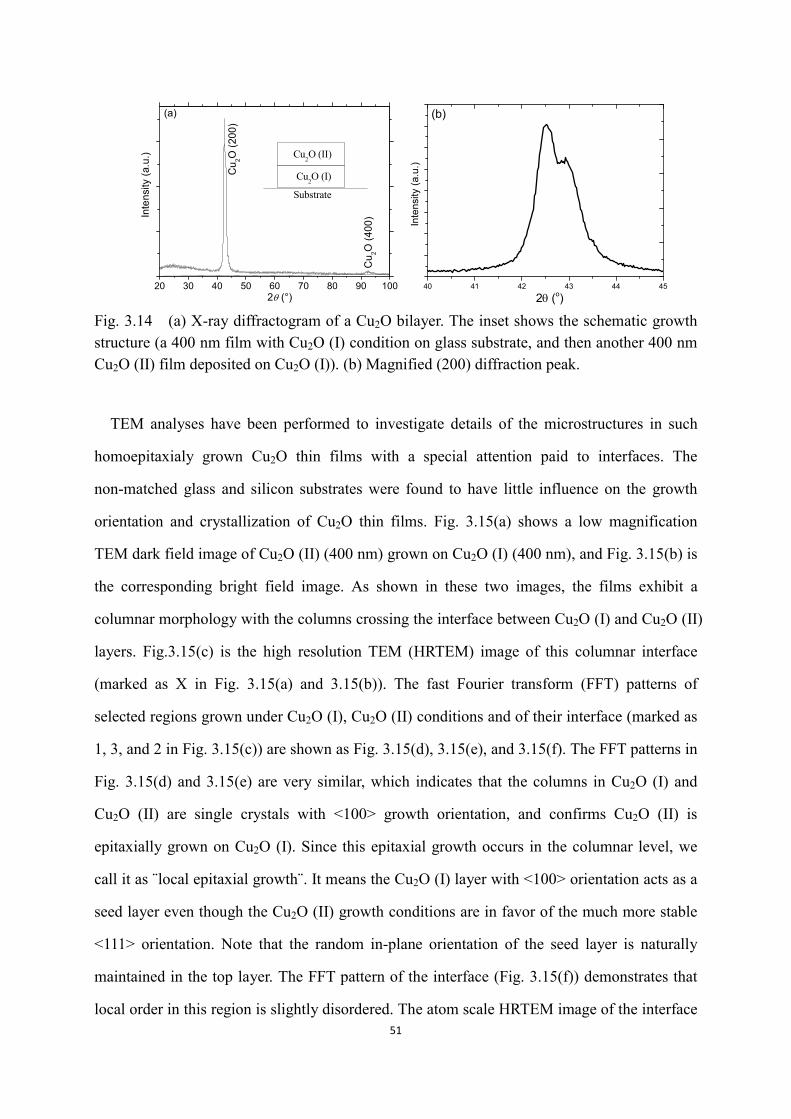
51
20 30 40 50 60 70 80 90 100
Cu2O (II)
Cu 2O
(400
)
Cu 2O
(200
)
Inte
nsity
(a.u
.)
2 (°)
Cu2O (I)
Substrate
(a)
40 41 42 43 44 45
Inte
nsity
(a.u
.)
2(o)
(b)
Fig. 3.14 (a) X-ray diffractogram of a Cu2O bilayer. The inset shows the schematic growth structure (a 400 nm film with Cu2O (I) condition on glass substrate, and then another 400 nm Cu2O (II) film deposited on Cu2O (I)). (b) Magnified (200) diffraction peak.
TEM analyses have been performed to investigate details of the microstructures in such
homoepitaxialy grown Cu2O thin films with a special attention paid to interfaces. The
non-matched glass and silicon substrates were found to have little influence on the growth
orientation and crystallization of Cu2O thin films. Fig. 3.15(a) shows a low magnification
TEM dark field image of Cu2O (II) (400 nm) grown on Cu2O (I) (400 nm), and Fig. 3.15(b) is
the corresponding bright field image. As shown in these two images, the films exhibit a
columnar morphology with the columns crossing the interface between Cu2O (I) and Cu2O (II)
layers. Fig.3.15(c) is the high resolution TEM (HRTEM) image of this columnar interface
(marked as X in Fig. 3.15(a) and 3.15(b)). The fast Fourier transform (FFT) patterns of
selected regions grown under Cu2O (I), Cu2O (II) conditions and of their interface (marked as
1, 3, and 2 in Fig. 3.15(c)) are shown as Fig. 3.15(d), 3.15(e), and 3.15(f). The FFT patterns in
Fig. 3.15(d) and 3.15(e) are very similar, which indicates that the columns in Cu2O (I) and
Cu2O (II) are single crystals with <100> growth orientation, and confirms Cu2O (II) is
epitaxially grown on Cu2O (I). Since this epitaxial growth occurs in the columnar level, we
call it as ¨local epitaxial growth¨. It means the Cu2O (I) layer with <100> orientation acts as a
seed layer even though the Cu2O (II) growth conditions are in favor of the much more stable
<111> orientation. Note that the random in-plane orientation of the seed layer is naturally
maintained in the top layer. The FFT pattern of the interface (Fig. 3.15(f)) demonstrates that
local order in this region is slightly disordered. The atom scale HRTEM image of the interface
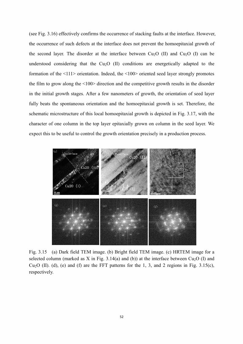
52
(see Fig. 3.16) effectively confirms the occurrence of stacking faults at the interface. However,
the occurrence of such defects at the interface does not prevent the homoepitaxial growth of
the second layer. The disorder at the interface between Cu2O (II) and Cu2O (I) can be
understood considering that the Cu2O (II) conditions are energetically adapted to the
formation of the <111> orientation. Indeed, the <100> oriented seed layer strongly promotes
the film to grow along the <100> direction and the competitive growth results in the disorder
in the initial growth stages. After a few nanometers of growth, the orientation of seed layer
fully beats the spontaneous orientation and the homoepitaxial growth is set. Therefore, the
schematic microstructure of this local homoepitaxial growth is depicted in Fig. 3.17, with the
character of one column in the top layer epitaxially grown on column in the seed layer. We
expect this to be useful to control the growth orientation precisely in a production process.
Fig. 3.15 (a) Dark field TEM image. (b) Bright field TEM image. (c) HRTEM image for a selected column (marked as X in Fig. 3.14(a) and (b)) at the interface between Cu2O (I) and Cu2O (II). (d), (e) and (f) are the FFT patterns for the 1, 3, and 2 regions in Fig. 3.15(c), respectively.

53
Fig. 3.16 (a) HRTEM image of the interfacebetween Cu2O (I) and Cu2O (II). (b) The magnified image of the selected square area in (a). The circles denote the structural defects.
Fig. 3.17 Schematic microstructure of local homoepitaxial growth with the characteristic of one column epitaxially grown on one column. Blue and red represent seed layer and top layer, respectively.
Fig. 3.18 shows the X-ray diffractogram of Cu2O (II) homoepitaxial films with different
thicknesses of Cu2O (I) seed layers. As shown in Fig. 3.18, a thickness of the seed layer equal
to or larger than 60 nm is required for homoepitaxial growth to occur. For the thinnest seed
layer, the <100> preferred orientation is not prominent, so the driving force for the growth
orientation from the seed layer is not as strong as that promoted from the intrinsic growth
conditions owing to Cu2O (II).
Local homoepitaxial relationship

54
20 30 40 50 60 70 80 90 100
(111
)
(200
)
160 nm Cu2O (I) + 400 nm Cu2O (II)
60 nm Cu2O (I) + 400 nm Cu2O (II)
40 nm Cu2O (I) + 400 nm Cu2O (II)
Inte
nsity
(a.u
.)
2 (°)
Fig. 3.18 X-ray diffractograms of homogrowth Cu2O films with different thicknesses of Cu2O (I) seed layers.
It is interesting to note that the contamination of the seed layer in air cannot block the
homoepitaxial growth. A Cu2O (I) seed layer with 400 nm is grown first, then the sputtering
chamber is open and the seed layer is exposed to air atmosphere. One hour later, the chamber
is closed and pumped to 10-4 Pa again. Subsequently, the Cu2O (II) layer (400 nm) was grown
on the air-exposed seed layer without any plasma cleaning. But X-ray diffractogram shows
that the homoepitaxial growth still exists (see Fig. 3.19).The contamination in air does not
prevent the homoepitaxial growth.
20 30 40 50 60 70 80 90 100
Cu 2O
(400
)
Cu 2O
(200
)
Inte
nsity
(a.u
.)
2(o)
Fig. 3.19 X-ray diffractogram of Cu2O (II) film homo-growth on air-exposed Cu2O (I).
The epitaxial growth of <100> has been clearly evidenced here above. To check that this
behavior can be extended to the <111> growth, a 400 nm-thick layer has been deposited using
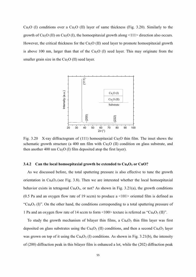
55
Cu2O (I) conditions over a Cu2O (II) layer of same thickness (Fig. 3.20). Similarly to the
growth of Cu2O (II) on Cu2O (I), the homoepitaxial growth along <111> direction also occurs.
However, the critical thickness for the Cu2O (II) seed layer to promote homoepitaxial growth
is above 100 nm, larger than that of the Cu2O (I) seed layer. This may originate from the
smaller grain size in the Cu2O (II) seed layer.
20 30 40 50 60 70 80 90 100
Cu2O (I)
Cu2O (II)
(222
)
(200
)(1
11)
Inte
nsity
(a.u
.)
2 (°)
Substrate
Fig. 3.20 X-ray diffractogram of (111) homoepitaxial Cu2O thin film. The inset shows the schematic growth structure (a 400 nm film with Cu2O (II) condition on glass substrate, and then another 400 nm Cu2O (I) film deposited atop the first layer).
3.4.2 Can the local homoepitaxial growth be extended to Cu4O3 or CuO?
As we discussed before, the total sputtering pressure is also effective to tune the growth
orientation in Cu4O3 (see Fig. 3.8). Then we are interested whether the local homoepitaxial
behavior exists in tetragonal Cu4O3, or not? As shown in Fig. 3.21(a), the growth conditions
(0.5 Pa and an oxygen flow rate of 19 sccm) to produce a <101> oriented film is defined as
“Cu4O3 (I)”. On the other hand, the conditions corresponding to a total sputtering pressure of
1 Pa and an oxygen flow rate of 14 sccm to form <100> texture is referred as “Cu4O3 (II)”.
To study the growth mechanism of bilayer thin films, a Cu4O3 thin film layer was first
deposited on glass substrates using the Cu4O3 (II) conditions, and then a second Cu4O3 layer
was grown on top of it using the Cu4O3 (I) conditions. As shown in Fig. 3.21(b), the intensity
of (200) diffraction peak in this bilayer film is enhanced a lot, while the (202) diffraction peak
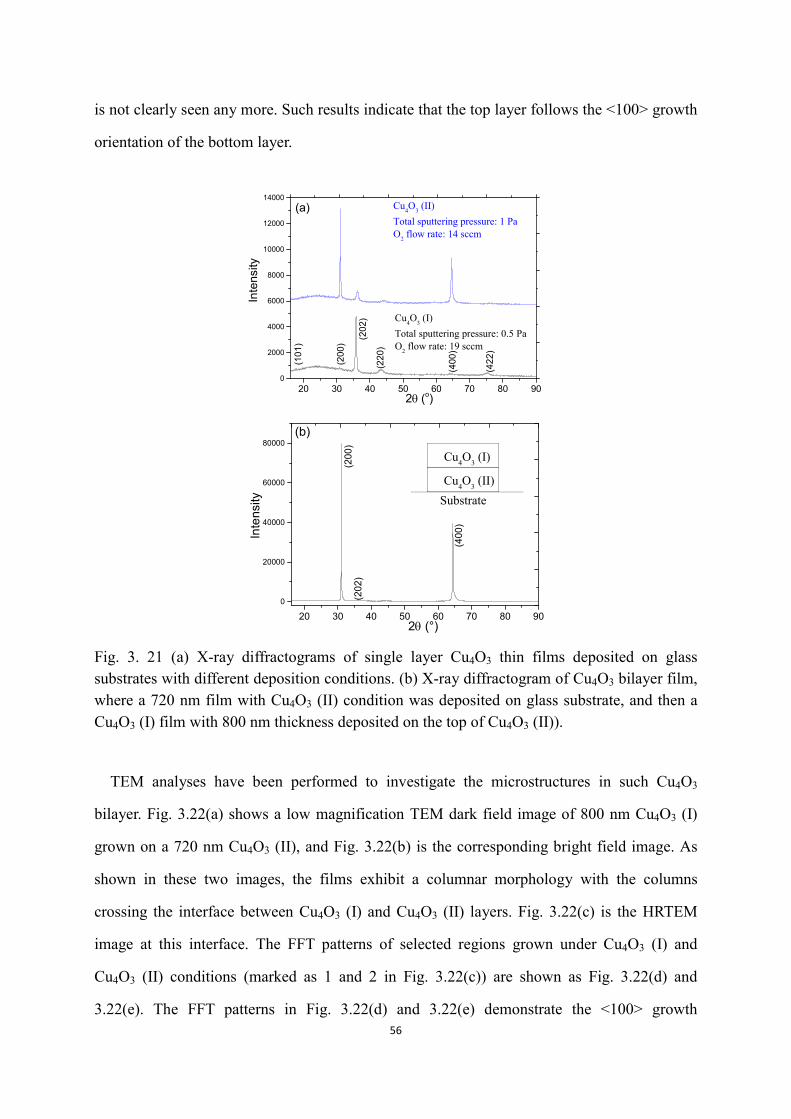
56
is not clearly seen any more. Such results indicate that the top layer follows the <100> growth
orientation of the bottom layer.
20 30 40 50 60 70 80 900
2000
4000
6000
8000
10000
12000
14000Cu4O3 (II)Total sputtering pressure: 1 PaO2 flow rate: 14 sccm
2(o)
Inte
nsity
(a)
Cu4O3 (I)Total sputtering pressure: 0.5 PaO2 flow rate: 19 sccm
(422
)
(400
)
(220
)
(202
)
(200
)
(101
)
20 30 40 50 60 70 80 900
20000
40000
60000
80000
(400
)
(202
)(2
00)
2 (°)
Inte
nsity
SubstrateCu4O3 (II)
Cu4O3 (I)
(b)
Fig. 3. 21 (a) X-ray diffractograms of single layer Cu4O3 thin films deposited on glass substrates with different deposition conditions. (b) X-ray diffractogram of Cu4O3 bilayer film, where a 720 nm film with Cu4O3 (II) condition was deposited on glass substrate, and then a Cu4O3 (I) film with 800 nm thickness deposited on the top of Cu4O3 (II)).
TEM analyses have been performed to investigate the microstructures in such Cu4O3
bilayer. Fig. 3.22(a) shows a low magnification TEM dark field image of 800 nm Cu4O3 (I)
grown on a 720 nm Cu4O3 (II), and Fig. 3.22(b) is the corresponding bright field image. As
shown in these two images, the films exhibit a columnar morphology with the columns
crossing the interface between Cu4O3 (I) and Cu4O3 (II) layers. Fig. 3.22(c) is the HRTEM
image at this interface. The FFT patterns of selected regions grown under Cu4O3 (I) and
Cu4O3 (II) conditions (marked as 1 and 2 in Fig. 3.22(c)) are shown as Fig. 3.22(d) and
3.22(e). The FFT patterns in Fig. 3.22(d) and 3.22(e) demonstrate the <100> growth
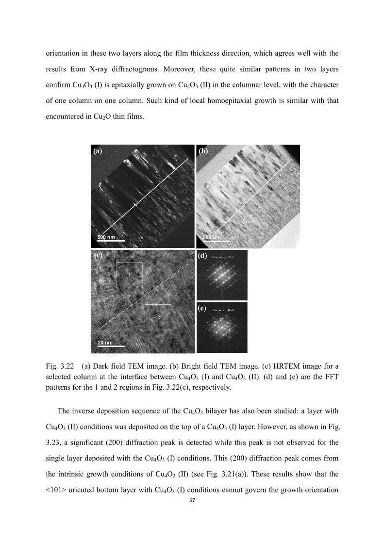
57
orientation in these two layers along the film thickness direction, which agrees well with the
results from X-ray diffractograms. Moreover, these quite similar patterns in two layers
confirm Cu4O3 (I) is epitaxially grown on Cu4O3 (II) in the columnar level, with the character
of one column on one column. Such kind of local homoepitaxial growth is similar with that
encountered in Cu2O thin films.
Fig. 3.22 (a) Dark field TEM image. (b) Bright field TEM image. (c) HRTEM image for a selected column at the interface between Cu4O3 (I) and Cu4O3 (II). (d) and (e) are the FFT patterns for the 1 and 2 regions in Fig. 3.22(c), respectively.
The inverse deposition sequence of the Cu4O3 bilayer has also been studied: a layer with
Cu4O3 (II) conditions was deposited on the top of a Cu4O3 (I) layer. However, as shown in Fig.
3.23, a significant (200) diffraction peak is detected while this peak is not observed for the
single layer deposited with the Cu4O3 (I) conditions. This (200) diffraction peak comes from
the intrinsic growth conditions of Cu4O3 (II) (see Fig. 3.21(a)). These results show that the
<101> oriented bottom layer with Cu4O3 (I) conditions cannot govern the growth orientation

58
of the top layer fully, which is different from that in Cu4O3 (I) grown on Cu4O3 (II). This
seems to indicate that this <101> oriented Cu4O3 bottom layer can hardly promote the local
homoepitaxial growth.
20 30 40 50 60 70 80 900
1000
2000
3000
4000
5000
2 (°)
(422
)(400
)
(220
)
(101
)
Inte
nsity
(200
)
(202
)
SubstrateCu4O3 (I)
Cu4O3 (II)
Fig. 3.23 X-ray diffractogram of a Cu4O3 bilayer with 800 nm Cu4O3 (II) film deposited on 800 nm Cu4O3 (I) layer.
Special growth conditions (0.9 Pa total sputtering pressure and 16 sccm O2 flow rate),
defined as “Cu4O3 (III)”, can produce single phase Cu4O3 thin films without notablely
preferred orientation, as shown in Fig. 3.24(a). In this case, both (200) and (202) diffractions
peaks are clearly evidenced. Then, a bilayer film with 800 nm Cu4O3 (I) deposited on 740 nm
Cu4O3 (III) is synthesized. Surprisingly, the X-ray diffractogram of this bilayer (see Fig.
3.24(b)), shows that the absolute intensity of (200) and (400) diffraction peaks, as well as the
relative intensity ratio between (200) and (202) peaks, are enhanced a lot. This implies that
the <100> growth orientation in the seed layer provides a strong driving force to set the
growth orientation of the top layer.
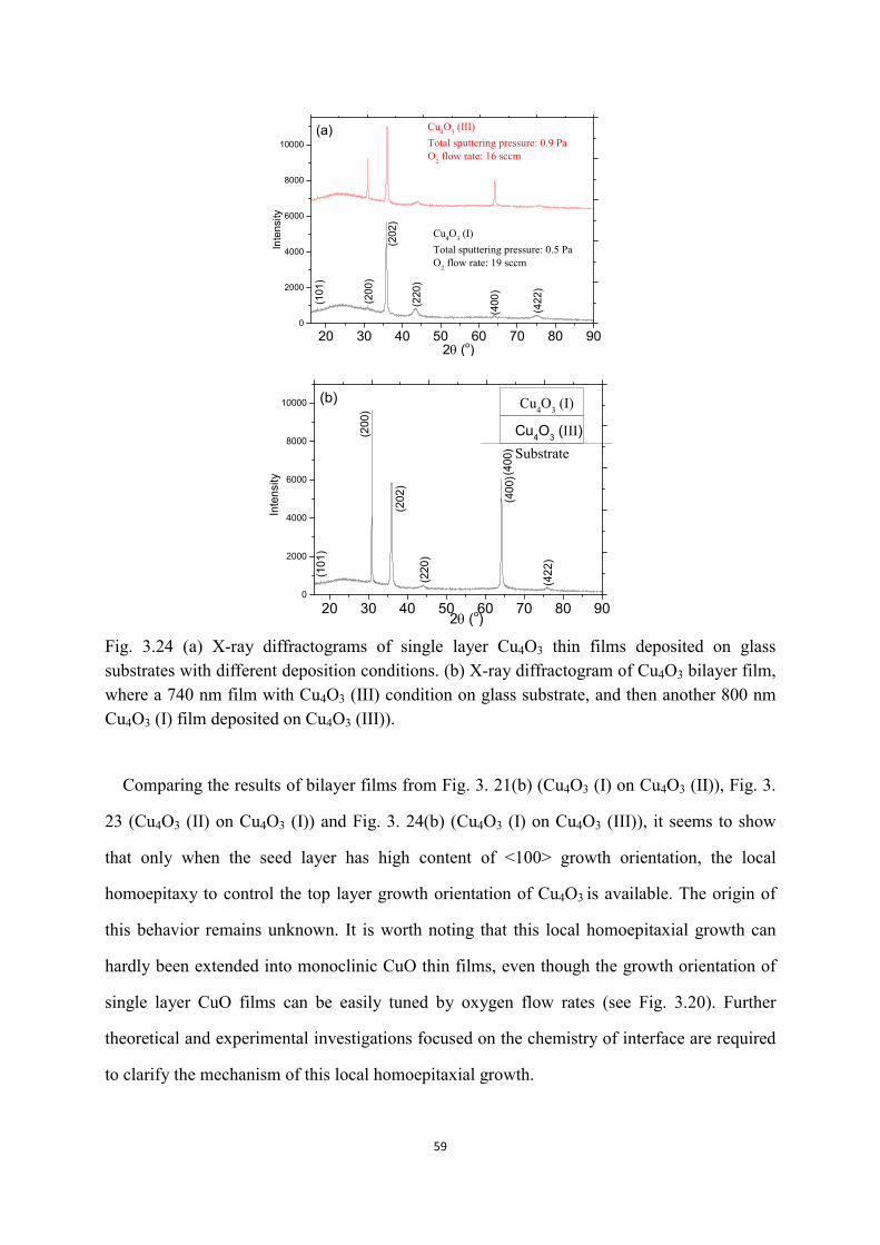
59
20 30 40 50 60 70 80 900
2000
4000
6000
8000
10000
(422
)
(400
)
(220
)
(202
)
(200
)
(101
)
Cu4O3 (III)Total sputtering pressure: 0.9 PaO2 flow rate: 16 sccm
Cu4O3 (I)Total sputtering pressure: 0.5 PaO2 flow rate: 19 sccm
2(o)
Inte
nsity
(a)
20 30 40 50 60 70 80 900
2000
4000
6000
8000
10000
(422
)
(400
)
(220
)
(202
)
(200
)
(101
)
2(o)
Inte
nsity
SubstrateCu4O3 (III)
Cu4O3 (I)
(400
)
(b)
Fig. 3.24 (a) X-ray diffractograms of single layer Cu4O3 thin films deposited on glass substrates with different deposition conditions. (b) X-ray diffractogram of Cu4O3 bilayer film, where a 740 nm film with Cu4O3 (III) condition on glass substrate, and then another 800 nm Cu4O3 (I) film deposited on Cu4O3 (III)).
Comparing the results of bilayer films from Fig. 3. 21(b) (Cu4O3 (I) on Cu4O3 (II)), Fig. 3.
23 (Cu4O3 (II) on Cu4O3 (I)) and Fig. 3. 24(b) (Cu4O3 (I) on Cu4O3 (III)), it seems to show
that only when the seed layer has high content of <100> growth orientation, the local
homoepitaxy to control the top layer growth orientation of Cu4O3 is available. The origin of
this behavior remains unknown. It is worth noting that this local homoepitaxial growth can
hardly been extended into monoclinic CuO thin films, even though the growth orientation of
single layer CuO films can be easily tuned by oxygen flow rates (see Fig. 3.20). Further
theoretical and experimental investigations focused on the chemistry of interface are required
to clarify the mechanism of this local homoepitaxial growth.
60
3.5 Local heteroepitaxial growth of NiO on Cu2O
NiO crystallizes in the cubic rocksalt structure (space group Fm
3m), where the Ni2+ and
O2- ions are six-fold coordinated. Along the <111> direction, NiO consists of alternative Ni2+
and O2- planes with Ni2+ or O2- as terminations, giving rise to a net surface charge and an
electric dipole moment (infinite surface energy) in the repeat unit perpendicular to the
{111}surfaces. This leads to the polar NiO {111} surfaces [100]–[102]. Accompanied by the
surface reconstruction (hydroxylation or adsorption of contamination beyond a simple bulk
truncation to stabilize the polarity [100]–[102]), the polar surfaces exhibit some unique
properties. For instance, NiO {111} surfaces, have larger work function than that of non-polar
{100} surfaces [103]. This enables to dramatically enhance the open circuit voltage and
power conversion efficiency in polymer bulk-heterojunction solar cells by inserting a <111>
oriented NiO thin film as anode interfacial layer [103], [104]. Different reactive magnetron
sputtering methods (including direct-current (DC), radio frequency (RF) and high-power
impulse magnetron sputtering (HiPIMS)) have been used to grow NiO thin films from
metallic Ni target, but most of them show <100> preferred orientation or non-preferred
orientation [105]–[107]. Thus, the growth of <111> oriented NiO thin films by reactive
sputtering on non-matched substrates at room temperature is still challenging.
The cubic Cu2O (space group Pn-3m) with lattice constant a of 0.427 nm in bulk has
similar structure with NiO (a = 0.417 nm in bulk). The lattice mismatch in the unit cell
between NiO and Cu2O is about 2.4 %. On the other hand, Cu2O {111} planes only contain
Cu atoms, which seems to be naturally matched with the polar NiO {111} planes. From these
crystallographic characters, it seems that the epitaxial criterias are fulfilled between Cu2O
{111} and NiO {111}. Hence, it is interesting to investigate the thin film growth mechanism
of a NiO layer deposited on top of a <111> oriented Cu2O layer at room temperature using the
reactive magnetron sputtering process.
X-ray diffractograms of single layer NiO thin films deposited on glass substrates with
different O2 flow rates are shown in Fig. 3.25(a), while the Ar flow rate is fixed at 25 sccm.
Within this range of oxygen flow rates, no metallic nickel is evidenced by XRD, indicating
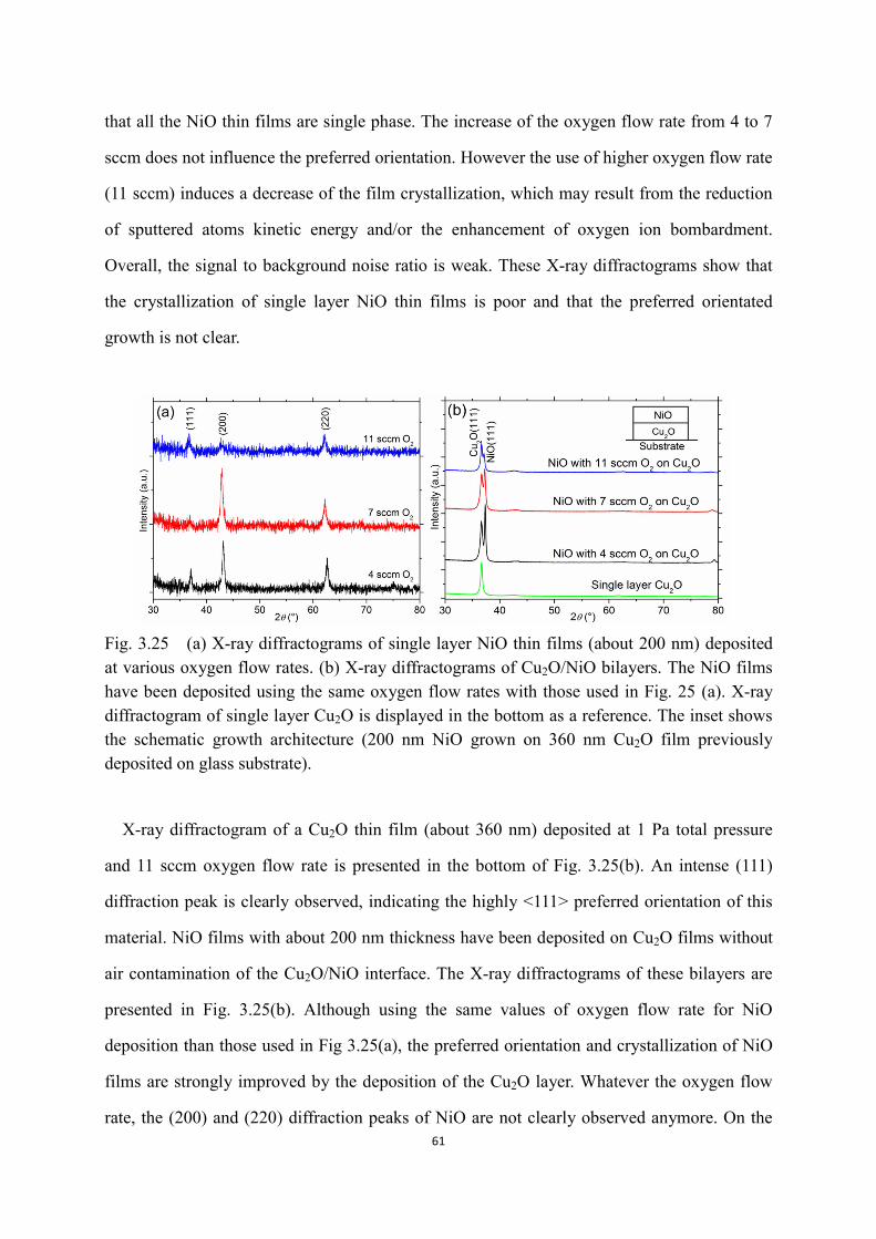
61
that all the NiO thin films are single phase. The increase of the oxygen flow rate from 4 to 7
sccm does not influence the preferred orientation. However the use of higher oxygen flow rate
(11 sccm) induces a decrease of the film crystallization, which may result from the reduction
of sputtered atoms kinetic energy and/or the enhancement of oxygen ion bombardment.
Overall, the signal to background noise ratio is weak. These X-ray diffractograms show that
the crystallization of single layer NiO thin films is poor and that the preferred orientated
growth is not clear.
Fig. 3.25 (a) X-ray diffractograms of single layer NiO thin films (about 200 nm) deposited at various oxygen flow rates. (b) X-ray diffractograms of Cu2O/NiO bilayers. The NiO films have been deposited using the same oxygen flow rates with those used in Fig. 25 (a). X-ray diffractogram of single layer Cu2O is displayed in the bottom as a reference. The inset shows the schematic growth architecture (200 nm NiO grown on 360 nm Cu2O film previously deposited on glass substrate).
X-ray diffractogram of a Cu2O thin film (about 360 nm) deposited at 1 Pa total pressure
and 11 sccm oxygen flow rate is presented in the bottom of Fig. 3.25(b). An intense (111)
diffraction peak is clearly observed, indicating the highly <111> preferred orientation of this
material. NiO films with about 200 nm thickness have been deposited on Cu2O films without
air contamination of the Cu2O/NiO interface. The X-ray diffractograms of these bilayers are
presented in Fig. 3.25(b). Although using the same values of oxygen flow rate for NiO
deposition than those used in Fig 3.25(a), the preferred orientation and crystallization of NiO
films are strongly improved by the deposition of the Cu2O layer. Whatever the oxygen flow
rate, the (200) and (220) diffraction peaks of NiO are not clearly observed anymore. On the

62
other hand, the 2 diffraction angles at about 36~37° show two contributions. The first part
located at approx. 36.6° is related to the Cu2O layer and the second part with higher
diffraction angle corresponds to the diffraction of the NiO (111) planes. Moreover, the
intensity of NiO (111) diffraction peaks in the bilayers are much more stronger than that in
single layer NiO thin films with the same thickness, demonstrating the better crystallization.
Such results indicate that the preferred orientation of Cu2O strongly governs that of the NiO
layer, regardless of the NiO deposition conditions. This means the Cu2O layer acts as a seed
layer, which can be used to tune the growth orientation of the top NiO layer. Finally, the NiO
(111) diffraction peak intensity in the bilayers with the same thickness has a tendency to
decrease with increasing the oxygen flow rate, which could be similar to the result observed
in single NiO layer.
TEM analyses have been performed to study the microstructure of bilayers. TEM images of
NiO deposited with 11 sccm O2 grown on Cu2O are presented in Fig. 3.26. Fig. 3.26(a) shows
the low magnification TEM bright field image, which demonstrates the columnar growth in
both NiO and Cu2O layers. The microdiffraction method has been employed to determine the
growth orientation. The microdiffraction patterns for NiO and Cu2O acquired from the regions
almost in a line along the film growth direction, are presented in Fig. 3.26(b) and (c),
respectively. Such similar patterns clearly show the heteroepitaxial growth occurs in columns
between these two layers. As seen in Fig. 3.26(b) and (c), the (111) planes in these two layers
are parallel to the substrate surface, which is in accordance with the results obtained by the
X-ray diffraction.
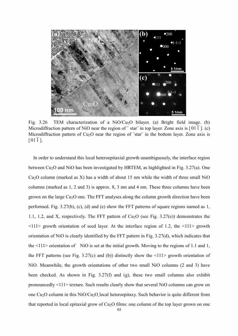
63
Fig. 3.26 TEM characterization of a NiO/Cu2O bilayer. (a) Bright field image. (b) Microdiffraction pattern of NiO near the region of ¨ star¨ in top layer. Zone axis is [ 101 ]. (c) Microdiffraction pattern of Cu2O near the region of ¨star¨ in the bottom layer. Zone axis is [ 101 ].
In order to understand this local heteroepitaxial growth unambiguously, the interface region
between Cu2O and NiO has been investigated by HRTEM, as highlighted in Fig. 3.27(a). One
Cu2O column (marked as X) has a width of about 15 nm while the width of three small NiO
columns (marked as 1, 2 and 3) is approx. 8, 3 nm and 4 nm. These three columns have been
grown on the large Cu2O one. The FFT analyses along the column growth direction have been
performed. Fig. 3.27(b), (c), (d) and (e) show the FFT patterns of square regions named as 1,
1.1, 1.2, and X, respectively. The FFT pattern of Cu2O (see Fig. 3.27(e)) demonstrates the
<111> growth orientation of seed layer. At the interface region of 1.2, the <111> growth
orientation of NiO is clearly identified by the FFT pattern in Fig. 3.27(d), which indicates that
the <111> orientation of NiO is set at the initial growth. Moving to the regions of 1.1 and 1,
the FFT patterns (see Fig. 3.27(c) and (b)) distinctly show the <111> growth orientation of
NiO. Meanwhile, the growth orientations of other two small NiO columns (2 and 3) have
been checked. As shown in Fig. 3.27(f) and (g), these two small columns also exhibit
pronouncedly <111> texture. Such results clearly show that several NiO columns can grow on
one Cu2O column in this NiO/Cu2O local heteroepitaxy. Such behavior is quite different from
that reported in local epitaxial grow of Cu2O films: one column of the top layer grown on one
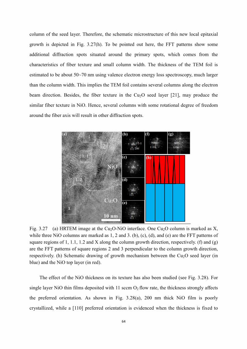
64
column of the seed layer. Therefore, the schematic microstructure of this new local epitaxial
growth is depicted in Fig. 3.27(h). To be pointed out here, the FFT patterns show some
additional diffraction spots situated around the primary spots, which comes from the
characteristics of fiber texture and small column width. The thickness of the TEM foil is
estimated to be about 50~70 nm using valence electron energy loss spectroscopy, much larger
than the column width. This implies the TEM foil contains several columns along the electron
beam direction. Besides, the fiber texture in the Cu2O seed layer [21], may produce the
similar fiber texture in NiO. Hence, several columns with some rotational degree of freedom
around the fiber axis will result in other diffraction spots.
Fig. 3.27 (a) HRTEM image at the Cu2O-NiO interface. One Cu2O column is marked as X, while three NiO columns are marked as 1, 2 and 3. (b), (c), (d), and (e) are the FFT patterns of square regions of 1, 1.1, 1.2 and X along the column growth direction, respectively. (f) and (g) are the FFT patterns of square regions 2 and 3 perpendicular to the column growth direction, respectively. (h) Schematic drawing of growth mechanism between the Cu2O seed layer (in blue) and the NiO top layer (in red).
The effect of the NiO thickness on its texture has also been studied (see Fig. 3.28). For
single layer NiO thin films deposited with 11 sccm O2 flow rate, the thickness strongly affects
the preferred orientation. As shown in Fig. 3.28(a), 200 nm thick NiO film is poorly
crystallized, while a [110] preferred orientation is evidenced when the thickness is fixed to

65
800 nm. This may originate from the stress value in single layer NiO. Using the Stoney’s
method, the compressive stress of a 200 nm thick NiO film is 2.2 ± 0.3 GPa. Higher NiO
thickness may accommodate part of the stress, consequently changing the preferred
orientation of NiO. The effect of the NiO thickness on its preferred orientation disappears
when the NiO film is deposited on a Cu2O seed layer (Fig. 3.28(b)). Whatever the NiO
thickness, only a <111> texture is evidenced for NiO deposited on Cu2O. The shape of the
diffraction peak in the 36-37° region is dependent on the NiO thickness. For a 200 nm value,
two diffraction peaks are observed as previously mentioned. The low angle peak is related to
the (111) planes of the Cu2O layer, while the high angle diffraction peak corresponds to the
(111) planes of NiO. On the other hand, only one wide diffraction peak is observed for a 800
nm thick NiO film deposited on a Cu2O one. Its position is ranging between those of (111)
Cu2O and (111) NiO. Such result can be explained considering a progressive change of the
NiO contribution due to a decrease of the compressive stress.
Fig. 3.28 (a) X-ray diffractograms of single layer NiO thin films with different thicknesses (200 nm and 800 nm) deposited at 11 sccm O2 flow rate. (b) X-ray diffractograms of NiO with different thicknesses deposited on Cu2O seed layer with a constant thickness. The inset shows the magnified (111) diffraction peak.
The influence of Cu2O seed layer thickness on the preferred orientation of NiO has been
also investigated. 200 nm NiO films using 11 sccm O2 have been deposited on Cu2O seed
layers with different thickness (60, 120 and 360 nm). The growth conditions (1 Pa total
pressure and 11 sccm O2 flow rate) to synthesize Cu2O have been employed. X-ray
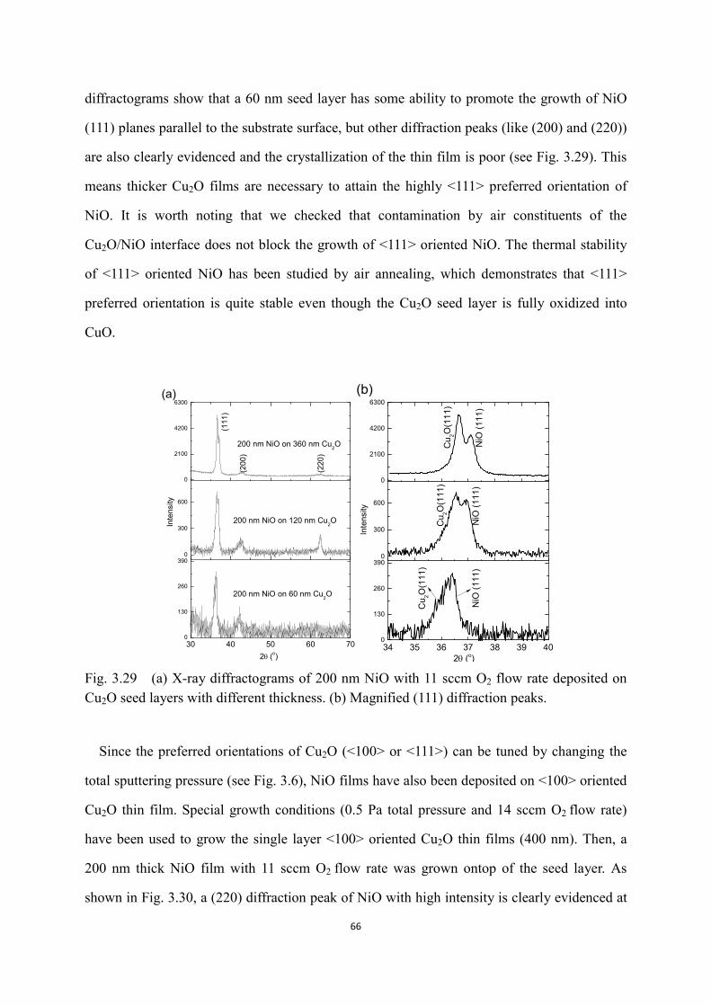
66
diffractograms show that a 60 nm seed layer has some ability to promote the growth of NiO
(111) planes parallel to the substrate surface, but other diffraction peaks (like (200) and (220))
are also clearly evidenced and the crystallization of the thin film is poor (see Fig. 3.29). This
means thicker Cu2O films are necessary to attain the highly <111> preferred orientation of
NiO. It is worth noting that we checked that contamination by air constituents of the
Cu2O/NiO interface does not block the growth of <111> oriented NiO. The thermal stability
of <111> oriented NiO has been studied by air annealing, which demonstrates that <111>
preferred orientation is quite stable even though the Cu2O seed layer is fully oxidized into
CuO.
30 40 50 60 700
130
260
3900
300
600
0
2100
4200
6300
2(o)
200 nm NiO on 60 nm Cu2O
200 nm NiO on 120 nm Cu2O Inte
nsity
200 nm NiO on 360 nm Cu2O
(220
)
(200
)
(111
)
(a)
34 35 36 37 38 39 400
130
260
3900
300
600
0
2100
4200
6300
NiO
(111
)
Cu 2O
(111
)
2(o)
Cu 2O
(111
)
NiO
(111
)
Inte
nsity
(b)
Cu 2O
(111
)
NiO
(111
)
Fig. 3.29 (a) X-ray diffractograms of 200 nm NiO with 11 sccm O2 flow rate deposited on Cu2O seed layers with different thickness. (b) Magnified (111) diffraction peaks.
Since the preferred orientations of Cu2O (<100> or <111>) can be tuned by changing the
total sputtering pressure (see Fig. 3.6), NiO films have also been deposited on <100> oriented
Cu2O thin film. Special growth conditions (0.5 Pa total pressure and 14 sccm O2 flow rate)
have been used to grow the single layer <100> oriented Cu2O thin films (400 nm). Then, a
200 nm thick NiO film with 11 sccm O2 flow rate was grown ontop of the seed layer. As
shown in Fig. 3.30, a (220) diffraction peak of NiO with high intensity is clearly evidenced at

67
approx. 62.6° as observed for NiO single layer, which indicates that this <100> oriented Cu2O
layer cannot fully support the local heteroepitaxial growth of <100> oriented NiO. This is out
of our expectation that NiO thin film would fully follow the <100> orientation of Cu2O.
Comparing such a result with the <111> texture of NiO thin film on <111> oriented Cu2O, it
is believed that the atomic structures or chemistry at the interface may play an important role
to drive the local heteroepitaxial growth. The surface terminations of Cu2O {111} could be Cu
or O atoms, but Cu or O atoms are not equivalent in the number and position (see Fig. 3.31).
However, the terminations of NiO {111} are Ni or O atoms, and they are equivalent in
number and position (see Fig. 3.31). The configurations of Cu atoms in {111} planes of Cu2O
are well matched with Ni or O atoms in {111} planes of NiO. Therefore, this local
heteroepitaxial growth could be qualitatively understood like this: Cu terminations in <111>
oriented Cu2O seed layer may prefer to form the banding with O atoms when depositing the
first layer of NiO, consequently giving rise to the polar <111> orientation with alternative Ni
and O layers along the growth direction. Moving onto the {100} planes of Cu2O, the surface
terminations are Cu or O atoms with non-equivalent number and position. But NiO {100} are
always composed of equivalent Ni and O atoms (see Fig. 3.31). This unmatched characteristic
between Cu2O and NiO {100} planes may introduce more defects and prevent the
heteroepitaxial growth. Further theoretical and experimental investigations focused on the
interface are required to clarify mechanism of this local heteroepitaxial growth.
30 40 50 60 70 800
3000
6000
9000
NiO
(220
)
Cu 2O
(200
)
Cu 2O
(111
) 200 nm NiO on Cu2O
Single layer Cu2O
Inte
nsity
2(o) Fig. 3.30 X-ray diffractogram of NiO on <100> oriented Cu2O thin film. The X-ray diffractogram of <100> oriented single layer Cu2O thin film is displayed as a reference.

68
Fig. 3.31 Atomic configurations of (111) and (001) planes in Cu2O (left) and NiO (right).
3.6 Chapter conclusions
In this chapter, we report the tunable growth in binary copper oxide thin films
synthesized by reactive magnetron sputtering at room temperature. A deposition diagram, to
describe the phase structure as a function of oxygen flow rate and total pressure, has been
attained by combining Raman spectrometry and X-ray diffraction. The total pressure can be
used to control the growth orientations of single phase Cu2O and Cu4O3 thin films due to their
narrow oxygen flow rate process windows. At low total pressure (0.5 Pa), Cu2O and Cu4O3
exhibit a preferred orientation along the directions with the highest surface energy: [100] and
[101], respectively. In contrast, planes with the lowest surface energy grow parallel to the
substrate surface when the total pressure is fixed at 1 Pa. For CuO films, the preferred
orientation can be controlled by the oxygen flow rate, i.e. by the oxygen stoichiometry.
Furthermore, the texture of the deposited films can also be controlled by the concept of
local homoepitaxial growth. During this kind of local homoepitaxial growth experiments, a
seed layer with preferred orientation is employed and another layer is deposited on top of it.
The seed layer governs the growth orientation of the top layer via the homoepitaxial growth in
columns with the character of one column on one column, independently of the deposition
conditions of top layer. Such a behavior can promote the <111> or <100> preferred growth
orientation in cubic Cu2O thin films. On the other hand, in tetragonal Cu4O3 thin films, this
kind of growth only produces the <100> texture and it fails to form <101> preferred
orientation. Besides, no local epitaxial growth has been evidenced in monoclinic CuO thin

69
films. A local heteroepitaxial growth with the character of several columns on one column has
been observed in bilayer films of NiO on Cu2O, which is effective to improve the
crystallization and to promote the <111> texture of NiO.

70

71
Chapter 4 Self-assembled growth of vertically aligned columnar
copper oxide nanocomposite thin films on unmatched substrates
4.1 Introduction
Nanocomposite thin films have attracted much attention due to their peculiar in a large
variety of applications, such as controlling the optical properties [108], [109], reducing the
dielectric loss [110]–[112], tuning the magnetic and electrical transport properties [113]–[119],
enhancing the electrochemical activity [120], [121], and increasing the hardness [122], [123].
The novel architecture, interfacial interplay, and interaction or coupling between the
nanocomposite constituents, are thought to be responsible for these peculiar properties and
new functionalities. The nanocomposite thin films are typically divided into four types from
the viewpoint of microstructure, including nanoparticles in matrix, lamellar multilayer,
columns in matrix and vertically aligned columnar nanocomposites[124]–[127]. Among them,
vertically aligned columnar nanocomposite, where all the phases have the columnar growth
along the film thickness direction, is particularly appealing as its larger interfacial area and
high availability of vertical strain control than other types [124], [125].
In the past decade, tremendous progress has been made in nanocomposite thin films about
designing interface-induced novel functionality. However, to the best of our knowledge, most
of investigations on vertically aligned columnar oxide nanocomposites are dedicated to
epitaxial films (one perovskite phase with another phase) grown on matched single-crystal
oxide substrates at high temperature by pulsed laser deposition [110], [112], [115], [116],
[118], [120], [124], [125]. Such matched single-crystal substrates are critical to promote the
separated and independent columnar growth for different phases. Their high cost and small
size, as well as the low homogeneous size of films deposited by pulsed laser deposition, are
not desirable for the large-area devices. Hence, in order to promote the application of
vertically aligned columnar nanocomposite thin films in different areas, it is attractive to
deposit such films on unmatched substrates using a low-cost method. Magnetron sputtering is
72
a standard manufacturing process associated with relatively low cost and easy fabrication of
large-area films. Sputtered films with single phase usually exhibit the columnar
microstructure [87], [122], [128]. However, this typical columnar structure will vanish with
the addition of a second phase, giving rise to a nanocrystalline composite [122]. Therefore, it
is challengeable to grow biphase composite thin films with vertically aligned columnar
structures on unmatched substrates by sputtering.
Binary copper oxides (Cu2O, Cu4O3 and CuO), as spontaneous p-type semiconductors,
have been widely studied [4], [5], [8], [27], [129]. More recently, some surprising properties
have been observed in the biphase copper oxide composite thin films. For instance, a lower
resistivity has been observed in biphase sputtered Cu2O + Cu4O3 thin films than in the single
phase Cu2O or Cu4O3 thin films [8]. In addition, the biphase Cu2O and Cu4O3 thin films can
enhance the photovoltaic activity significantly in a binary copper oxide (Cu-O) light absorber
[129]. However, the origin of these peculiar properties remains unknown.
In this work, for the first time, we demonstrate the vertically aligned columnar
microstructure of biphase Cu2O and Cu4O3 thin films on unmatched glass or silicon substrates
grown by reactive magnetron sputtering. Finally, the unusual electrical properties of biphase
thin films are discussed.
4.2 Vertically aligned columnar growth in biphase Cu2O and Cu4O3 thin
films
4.2.1 Identifying the phases by X-ray diffraction and Raman spectrometry
The diffractograms of copper oxide thin films deposited with different oxygen flow rates
are presented in Fig. 4.1(a). Whatever the oxygen flow rate, two main diffraction peaks are
observed at approx. 36° and 42°. The first peak may be due to the diffraction of Cu2O (111)
planes or Cu4O3 (202) or (004) planes and the peak located close to 42° may be related to
Cu2O (200) or Cu4O3 (220), as the d values in Cu2O and Cu4O3 are quite close in certain
planes (See Table 1.1). To obtain a more precise structural description of the films,
micro-Raman spectrometry was used (see Fig. 4.1(b)). The film deposited with 14 sccm

73
oxygen shows a typical Raman spectrum of Cu2O, where the T2g band is observed close to
520 cm-1. The bands at 93, 147 and 216 cm-1 are related to defects, non-stoichiometry and
resonant excitation in Cu2O [22]. A new band close to 531 cm-1 is evidenced when the oxygen
flow rate is 15 sccm, which has been assigned to A1g mode of Cu4O3 [19], [22]. Its intensity
increases with the increase of oxygen flow rate while the bands related to Cu2O decrease
progressively. Hence, these Raman spectra clearly evidence that the films deposited with
15-18 sccm range are biphase Cu2O + Cu4O3, and that the fraction of Cu4O3 can be controlled
by adjusting the oxygen flow rate.
20 30 40 50 60 70 80 90 100
(400
)
(220
)
(202
)
(200
)
(101
)
(200
)
(111
)
19 sccm O2: Cu
4O
3
18 sccm O2: Cu
2O+Cu
4O
3
17 sccm O2: Cu2O+Cu4O3
16 sccm O2: Cu2O+Cu4O3
15 sccm O2: Cu2O+Cu4O3
Inte
nsity
(a.u
.)
2(o)
14 sccm O2: Cu2O
(a)
100 200 300 400 500 600 700
100 200 300 400 500 600 700
610 cm-1520 cm-1216 cm-1
147 cm-193 cm-1
Raman shift (cm-1)
14 sccm O2: Cu2O
534 cm-1
15 sccm O2: Cu2O+Cu4O3
313 cm-1531 cm-1
16 sccm O2: Cu2O+Cu4O3
310 cm-1531 cm-117 sccm O2: Cu2O+Cu4O3
92 cm-1
313 cm-1
534 cm-118 sccm O2: Cu2O+Cu4O3
505 cm-1531 cm-1
311 cm-1
19 sccm O2: Cu4O3
Inte
nsity
(a.u
.)
(b)
Fig. 4.1 (a) X-ray diffractograms and (b) Raman spectra of copper oxide thin films deposited with different oxygen flow rates.
4.2.2 Cross-sectional microstructure of biphase Cu2O and Cu4O3 thin films
To study the microstructure of the biphase thin films, TEM analyses were carried out firstly
in the cross-section. The cross-sectional TEM images of biphase Cu4O3 and Cu2O thin film
deposited with 17 sccm O2 are shown in Fig. 4.2. Electron diffraction pattern on a large area is
presented in Fig. 4.2(a), which can hardly distinguish Cu2O and Cu4O3 phases as they exhibit
close d values (see Table 1.1). Surprisingly, the dark and bright filed images in Fig. 4.2(a) and
(b) show a columnar growth in the growth mode of zone T for this biphase film, and the
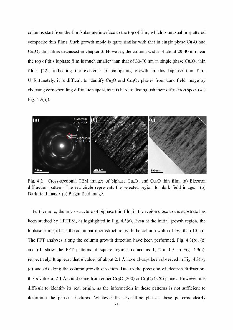
74
columns start from the film/substrate interface to the top of film, which is unusual in sputtered
composite thin films. Such growth mode is quite similar with that in single phase Cu2O and
Cu4O3 thin films discussed in chapter 3. However, the column width of about 20-40 nm near
the top of this biphase film is much smaller than that of 30-70 nm in single phase Cu4O3 thin
films [22], indicating the existence of competing growth in this biphase thin film.
Unfortunately, it is difficult to identify Cu2O and Cu4O3 phases from dark field image by
choosing corresponding diffraction spots, as it is hard to distinguish their diffraction spots (see
Fig. 4.2(a)).
Fig. 4.2 Cross-sectional TEM images of biphase Cu4O3 and Cu2O thin film. (a) Electron diffraction pattern. The red circle represents the selected region for dark field image. (b) Dark field image. (c) Bright field image.
Furthermore, the microstructure of biphase thin film in the region close to the substrate has
been studied by HRTEM, as highlighted in Fig. 4.3(a). Even at the initial growth region, the
biphase film still has the columnar microstructure, with the column width of less than 10 nm.
The FFT analyses along the column growth direction have been performed. Fig. 4.3(b), (c)
and (d) show the FFT patterns of square regions named as 1, 2 and 3 in Fig. 4.3(a),
respectively. It appears that d values of about 2.1 Å have always been observed in Fig. 4.3(b),
(c) and (d) along the column growth direction. Due to the precision of electron diffraction,
this d value of 2.1 Å could come from either Cu2O (200) or Cu4O3 (220) planes. However, it is
difficult to identify its real origin, as the information in these patterns is not sufficient to
determine the phase structures. Whatever the crystalline phases, these patterns clearly

75
demonstrate that the columns have almost the same growth orientation along the film
thickness.
Fig. 4.3 (a) HRTEM image of biphase thin film deposited with 17 sccm O2 at the initial growth region. Along the column growth direction, three square regions are marked as 1, 2 and 3. (b), (c) and (d) are the FFT patterns of square regions 1, 2 and 3 in (a), respectively. The red circles in (b), (c) and (d) represent the diffraction spots along the column growth direction, with the d values of about 2.1 Å.
Similar situations have been observed in columns with growth orientation of Cu2O <111>
or Cu4O3 <101>, as shown in Fig. 4.4. Fig. 4.4(a) is the HRTEM image close to the substrate,
while Fig. 4.4(b), (c) and (d) are the FFT patterns of square regions marked as 1, 2 and 3 in
Fig. 4.4(a). d values of about 2.4 Å in Fig. 4.4(b), (c) and (d) belong to Cu2O (111) or Cu4O3
(202). Hence, the columnar microstructure in the biphase thin film is formed at the initial
growth, and the columns have almost the same growth orientation along the film thickness. To
be pointed out here, the FFT patterns in Fig. 4.3 and 4.4 are typical in polycrystalline thin
films, which originate from the characteristics of small column width and fiber texture. The
thickness of the TEM foil is estimated to be about 50-70 nm by valence electron energy loss
spectroscopy, much larger than the column width near the substrate, which indicates that there
are several columns along the TEM thin foil thickness direction at the interface region.
Besides, the fiber texture observed in single phase Cu2O or Cu4O3 thin films, may exist in this
biphase thin film. Hence, several columns with some rotational degree of freedom around the
fiber axis will result in poor diffraction spots.
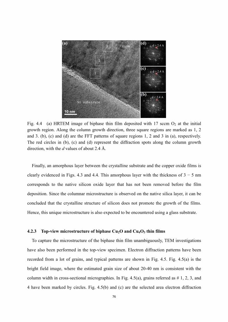
76
Fig. 4.4 (a) HRTEM image of biphase thin film deposited with 17 sccm O2 at the initial growth region. Along the column growth direction, three square regions are marked as 1, 2 and 3. (b), (c) and (d) are the FFT patterns of square regions 1, 2 and 3 in (a), respectively. The red circles in (b), (c) and (d) represent the diffraction spots along the column growth direction, with the d values of about 2.4 Å.
Finally, an amorphous layer between the crystalline substrate and the copper oxide films is
clearly evidenced in Figs. 4.3 and 4.4. This amorphous layer with the thickness of 3 − 5 nm
corresponds to the native silicon oxide layer that has not been removed before the film
deposition. Since the columnar microstructure is observed on the native silica layer, it can be
concluded that the crystalline structure of silicon does not promote the growth of the films.
Hence, this unique microstructure is also expected to be encountered using a glass substrate.
4.2.3 Top-view microstructure of biphase Cu2O and Cu4O3 thin films
To capture the microstructure of the biphase thin film unambiguously, TEM investigations
have also been performed in the top-view specimen. Electron diffraction patterns have been
recorded from a lot of grains, and typical patterns are shown in Fig. 4.5. Fig. 4.5(a) is the
bright field image, where the estimated grain size of about 20-40 nm is consistent with the
column width in cross-sectional micrographies. In Fig. 4.5(a), grains referred as # 1, 2, 3, and
4 have been marked by circles. Fig. 4.5(b) and (c) are the selected area electron diffraction

77
(SAED) patterns of grains # 1 and 2, respectively, which clearly shows that these two grains
are single crystal Cu4O3. Since the zone axis of grains # 1 and 2 are different, there is no in
plane orientation of Cu4O3 grains. The SAED pattern of grain # 3 is presented in Fig. 4.5(d),
which is the characteristic of Cu2O. As the grain size is too small, some additional diffraction
spots situated around the primary spots of single crystal Cu2O have been observed. Then, the
convergent beam electron diffraction (CBED) has been performed to the quite small grain # 4
and the pattern (see Fig. 4.5(e)) clearly manifests that this small grain is single crystal Cu2O.
A lot of single crystal grains have been selected to perform electron diffraction. Cu4O3 grains
exhibit the zone axes of [101], [110], [100], and [-13-1], while all the measured Cu2O grains
have the zone axis of [111]. The single crystal characteristic has also been confirmed by the
HRTEM images. As shown in Fig. 4.6, a single crystal Cu2O grain is clearly evidenced by the
FFT pattern.
Fig. 4.5 Top-view TEM images of biphase Cu4O3 and Cu2O thin film with 17 sccm O2. (a) Bright field image. (b), (c) and (d) are the SAED patterns of grains #1, #2 and #3 in Fig. 5(a), respectively. (e) The CBED pattern of grain #4.

78
Fig. 4.6 Top-view HRTEM image of biphase Cu4O3 and Cu2O thin film with 17 sccm O2. The inset shows the FFT pattern of the selected Cu2O grain marked by red line.
4.2.3 Discussion on the vertically aligned columnar growth mechanism
The above TEM micrographies from cross-section and top-view indicate an unusual
microstructure in biphase Cu4O3 and Cu2O thin films where the two phases grow
independently in columnar shape. Such a microstructure is strongly different from the
traditional concept that one phase is embedded into the second one that acts as matrix. Hence,
the schematic microstructure of this biphase thin film is depicted in Fig. 4.7; for simplicity,
we show an ordered arrangement of phases. As shown in Fig. 4.7, both phases just grow
separately and independently with the columnar microstructure along the whole film
thickness. This kind of unusual growth can be understood from the viewpoint of Cu2O local
homoepitaxial growth behavior reported in Chapter 3. In reactively sputtered growth of Cu2O
thin films, the Cu2O seed layer has a strong driving force to promote the subsequent growth
with the same growth orientation, independently of the deposition conditions [21]. Therefore,
in this biphase thin film, the growth process can be assumed: (1) due to intermediate oxygen
flow rate between those required to grow single phase Cu2O and Cu4O3, some Cu2O nucleus
are formed; (2) the strong driving force resulting from the local epitaxial growth induces a

79
selective formation of Cu2O on the nucleus with the same structure; (3) the local decrease of
the oxygen concentration induces a segregation of oxygen adatoms towards columns with
higher oxygen concentration that crystallizes in the Cu4O3 structure. Consequently, Cu4O3 and
Cu2O phases with columnar structures grow independently.
Fig. 4.7 Schematic microstructure of the biphase Cu4O3 and Cu2O thin film. For simplicity, we show an ordered arrangement of phase.
As reported in Chapter 3, the oxygen flow rate allows to tune the phase structure of copper
oxide films. The increase of the oxygen flow rate induces the deposition of Cu2O, Cu4O3 and
CuO. Moreover, between these single phases, biphase Cu2O + Cu4O3 and Cu4O3 + CuO films
can also be synthesized. The structure and the microstructure of Cu4O3 + CuO films have also
been studied by XRD, Raman and TEM. Films deposited with 21 sccm O2 are X-ray
amorphous (Fig. 4.8(a)), but Raman analyses clearly evidence the existence of Cu4O3 A1g
mode close to 532 cm-1 and CuO Ag mode at about 288 cm-1 (Fig. 4.8(b)) [19], [22].
Compared to Cu2O + Cu4O3 biphase films, the Cu4O3 + CuO biphase film shows different
microstructure. The cross-sectional TEM images demonstrate that the columnar growth in
biphase Cu4O3 + CuO thin film is not clear (see Fig. 4.9). Besides, the electron diffraction
pattern in Fig. 4.9(a) does not exhibit preferred orientation along film thickness, which is
different from that in Cu2O + Cu4O3 biphase films. Moreover, the top-view electron
diffraction patterns can hardly identify the single crystal features of grains. Hence, the
vertically aligned columnar growth mechanism is not encountered in this biphase Cu4O3 +

80
CuO film anymore. This result can also be explained by taking into account the local
homoepitaxial growth effect. Indeed, the texture of CuO films is mainly governed by the
oxygen partial pressure. Thus, a local change of the oxygen concentration induces a change of
the CuO preferred orientation that comes with a nucleation of a new grain without structural
relationship with the previous one. Consequently, there is no local homoepitaxial growth
behavior in this oxide. In the case of Cu4O3 phase, the [101] orientation deposited at 0.5 Pa
does not allow the local homoepitaxial growth effect. Considering the occurrence of local
homoepitaxial growth effect in Cu2O thin films, the vertically aligned columnar growth
mechanism in biphase Cu2O + Cu4O3 films can be well described, while this growth
mechanism does not exist in biphase Cu4O3 + CuO ones. Within this discussion, it is believed
that this vertically aligned columnar growth can also be extended to other materials with
certain requirements summarized as below:
- The system has to contain at least two stable or metastable phases,
- Each phase has to be deposit in crystalline form within the deposition conditions,
- The growth rate of each phase has to be close. Within the Cu-O system, the growth
rate of Cu2O is close to that of Cu4O3, while that of CuO is relatively low (poisoning
effect of the target) [22], [29],
- At least one phase should be grown independently with a local epitaxial growth
mechanism,
- The chemical compositions of the phases must be close, in order to allow the
segregation of one adsorbed element on the growing surface.
20 30 40 50 60 70 80 90 100
Inte
nsity
(a.u
.)
2 (°)
(a)
100 200 300 400 500 600 700
532 cm-1
288 cm-1
Inte
nsity
(a.u
.)
Raman shift (cm-1)
(b)
Fig. 4.8 (a) X-ray diffractogram and (b) Raman spectrum of biphase Cu4O3 + CuO film.

81
Fig. 4.9 Cross-sectional TEM micrographies of biphase Cu4O3 and CuO thin film. (a) Electron diffraction pattern. The red circle represents the selected region for dark field image. (b) Dark field image. (c) Bright field image.
4.3 Electrical properties of biphase Cu2O + Cu4O3 thin films
The room temperature resistivity of copper oxide thin films as a function of oxygen flow
rate is depicted in Fig. 4.10, which clearly reveals that the biphase thin film has lower
resistivity than single phase films. This result is in agreement with that reported by Meyer et
al. [8]. Since these thin films are deposited at room temperature, the hole mobility is
extremely low and it is difficult to determine the carrier concentration by Hall effect
measurements. For the single phase Cu2O or Cu4O3 thin films, the room temperature
resistivity decreases with the increase of oxygen flow rate (see Fig. 4.10), which could be
qualitatively understood from the defect mechanism. Taking Cu2O as an example, copper
vacancy (V ) is the predominant defects to produce the hole carriers, while the formation
energy of copper vacancy decreases in the oxygen rich conditions (higher oxygen flow rate)
[41], [42], [56]. Then the lower resistivity of single phase Cu2O thin films with higher oxygen
flow rate can be interpreted from its larger carrier concentration due to the reduction of copper
vacancy formation energy. In the case of biphase Cu2O and Cu4O3 thin film, the oxygen flow
rate is higher than that required to synthesis the single Cu2O phase. Thus the Cu2O columns
may have higher carrier concentrations. In contrast, the Cu4O3 columns may have lower
carrier concentration as the oxygen sub-stoichiometry. Consequently, the columns with
different carrier concentration (high carrier concentration and low carrier concentration)

82
arrange randomly, and their interface coupling may play a role for this kind of lower
resistivity. Further investigations are required to clarify this unusual phenomenon.
12 13 14 15 16 17 18 19 20
10
100
1000
Single phase Cu2O Biphase Cu2O and Cu4O3
Single phase Cu4O3
Res
istiv
ity (O
hm c
m)
Oxygen flow rate (sccm)
Fig. 4.10 Resistivity of copper oxide thin films as a function of oxygen flow rate.
4.4 Chapter Conclusions
Biphase Cu2O and Cu4O3 thin films have been characterized by TEM from cross-section
and top-view, which shows an unusual microstructure that both phases have the vertically
aligned columnar growth along the whole film thickness direction. This microstructure may
result from the local homoepitaxial growth of Cu2O. The intermediate oxygen flow rate
between those required to grow single phase Cu2O and Cu4O3 produce some Cu2O nucleus,
and then the strong driving force resulting from the local homoepitaxial growth induces a
selective formation of Cu2O on the nucleus with the same structure, giving rise to this kind of
unusual vertically aligned columnar microstructure. The lower resistivity has been observed
in the biphase thin films, which may be due to the interface coupling between Cu2O and
Cu4O3 columns. Such a unique microstructure has not been observed in Cu4O3 + CuO films.
This negative result may come from the lack of local epitaxial growth mechanism in single
CuO films. Finally, some requirements for the self-aligned columnar nanocomposite thin
films on unmatched substrates have been proposed.
83
Chapter 5 Optical properties and electronic structure of copper
oxide thin films
5.1 Introduction
Although the stable phase of Cu2O and CuO have been widely studied for the past three
decades both experimentally [8], [29], [130]–[134] and theoretically [2], [24]–[26], [42], [56],
[135], [136], there are still divergent reports regarding their electronic structure. For instance,
different calculation methods have precisely predicted the direct band gap of about 2 eV in
Cu2O, but their ground-state electronic structure and band ordering exhibit striking
discrepancies [24], [26], [136]. In the case of CuO, the type of band gap (direct or indirect)
remains controversial [5], [32], [33], [132], [134], [135], while the valence band density of
states (DOSs) calculated by different methods show notable difference [25], [33], [135]. On
the other hand, the meta-stable phase Cu4O3 (paramelaconite), an intermediate compound
between Cu2O and CuO, has received less attention [22], [25], [28], [29], [31], giving rise to a
mysterious veil. Local density approximation (LDA) with an additional potential U and
Heyd-Scuseria-Erzerhof (HSE) functionals have been employed to calculate its electronic
structure, whereas the resulting band gaps and DOSs are ambiguous [25], [28]. Besides, to the
best of our knowledge, little is known about electronic structure of Cu4O3 from an
experimental point of view.
Since the applications of copper oxides for energy conversion are closely linked to
electronic structure, their unclear properties will restrict further developments. Hence, it is of
great interest to investigate their electronic structure by a joint experimental and theoretical
study. Photoemission spectroscopies with different photon energies are well-known
technologies to determine the valence band electronic structure via the measurement of
kinetic energy spectra of emitted photoelectrons by the photoelectric effect. On the other hand,
the optical band gap is usually estimated by spectrophotometry from transmission (T) and

84
reflectance (R) measurements, which possesses higher precision and convenience than other
optical methods, e.g., ellipsometry, especially with the presence of sub-gap absorption, as it
does not require complex fitting. In the case of conduction band structure, electron energy
loss spectroscopy (EELS) has rapidly grown to be a useful technique to study the unoccupied
electronic states, as its great advantages of large penetration depth and high spatial resolution.
For the EELS measurement, electrons are ejected from core states to unoccupied states [83],
which provides the basis for a comparison between experimental empty states and theoretical
conduction band states, within the consideration of dipole selection rules.
Many-body perturbation theory in the GW (Green’s function calculations with screened
Coulomb interaction W) approximation has emerged as a standard computational tool to
predict the electronic structure of semiconductors and insulators, yielding systematical
improvements with respect to other methods [24], [26], [137]–[139]. Although various GW
schemes have been introduced and contested for transition metal (TM) oxides, a single
universal scheme that can describe the band structure reliably for a wide range of TM oxides,
is not yet available. Recently, a GW scheme with local-field effect and an empirical on-site
potential for TM d orbitals with a single parameter per TM cation (noted as GWLF + Vd), has
been proposed, which allows for reasonably predictive band gaps for different oxide
stoichiometries and TM oxidation states at an acceptable computational expense [24].
However, the band gap is just one characteristic of electronic structure of a semiconductor or
insulator, which does not contain sufficient information to conclude the whole electronic
structures.
In this work, the influence of air annealing effect on the optical and electrical properties of
Cu2O thin films has been studied in a first step. Then, we have investigated the electronic
structure of Cu2O, Cu4O3 and CuO from experiments and theoretical calculations. The optical
band gap, full DOSs in the valence band and partial DOSs in the conduction band are
determined by optical absorption, UPS and EELS spectroscopies, respectively. Meanwhile the
electronic structures and absorption coefficients calculated by GWLF + Vd approach, are
compared with experimental results and other reported calculations.

85
5.2 Transmittance enhancement and optical bandgap widening of Cu2O
thin films after air annealing
5.2.1 Phase structure evolution
X-ray diffractograms of as-deposited and air annealed Cu2O thin films deposited on glass
substrates are shown in Fig. 5.1 (a). The annealing duration has been fixed to 1 hour. When
the annealing temperature is lower than 300 °C, only Cu2O diffraction peaks are evidenced,
indicating that these thin films remain single phased. Once the temperature is equal or higher
than 300 °C, weak CuO diffraction peaks are observed. This result confirms that the
temperature to oxidize Cu2O into CuO in air is about 300 °C, which is consistent with earlier
reports [29], [76]. Raman analyses (not shown here) have verified the phase structures of thin
films. The magnified (200) diffraction peaks of Cu2O thin films are depicted in Fig. 5.1 (b). A
gradual shift towards higher angle values with increasing annealing temperature is evidenced.
Without considering the internal stress effect on the diffraction peak position, this behavior
may come from the decrease of the lattice constant from 0.43041 nm (as-deposited) to
0.43019 nm (180 °C), 0.42937 nm (260 °C), 0.42844 nm (280 °C), 0.42801 nm (300 °C), and
0.42800 (320 °C). In comparison with the lattice constant of bulk Cu2O (0.427 nm), the
shrinkage of lattice constant is due to the removal of some structural defects. X-ray
diffractogram of the Cu2O thin film annealed in vacuum at 200 °C (not shown here) indicates
that the film still has the single phase structure with the lattice constant of 0.43216 nm.
20 30 40 50 60 70 80 90 100
(a)
: CuO (002)
: CuO (111)
: Cu2O (111)
Cu 2O
(400
)
Cu 2O
(200
)
320 oC
300 oC
280 oC
260 oC
180 oC
As-deposited
Inte
nsity
(a.u
.)
2 (°)
41.6 41.8 42.0 42.2 42.4 42.6 42.8 43.0
(b)
320 oC
300 oC280 oC
260 oC
180 oC
As-deposited
Inte
nsity
(a.u
.)
2 (°)
Fig.5.1 (a) X-ray diffractograms of as-deposited and air annealed Cu2O thin films. (b) Magnified (200) diffraction peaks of Cu2O thin films.
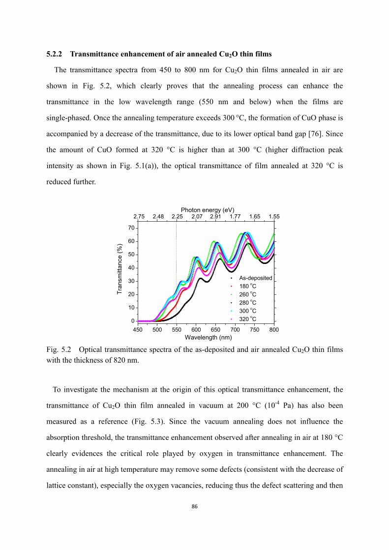
86
5.2.2 Transmittance enhancement of air annealed Cu2O thin films
The transmittance spectra from 450 to 800 nm for Cu2O thin films annealed in air are
shown in Fig. 5.2, which clearly proves that the annealing process can enhance the
transmittance in the low wavelength range (550 nm and below) when the films are
single-phased. Once the annealing temperature exceeds 300 °C, the formation of CuO phase is
accompanied by a decrease of the transmittance, due to its lower optical band gap [76]. Since
the amount of CuO formed at 320 °C is higher than at 300 °C (higher diffraction peak
intensity as shown in Fig. 5.1(a)), the optical transmittance of film annealed at 320 °C is
reduced further.
450 500 550 600 650 700 750 8000
10
20
30
40
50
60
70
Photon energy (eV)1.551.652.91 1.772.072.252.482.75
Tran
smitt
ance
(%)
Wavelength (nm)
As-deposited 180 oC 260 oC 280 oC 300 oC 320 oC
Fig. 5.2 Optical transmittance spectra of the as-deposited and air annealed Cu2O thin films with the thickness of 820 nm.
To investigate the mechanism at the origin of this optical transmittance enhancement, the
transmittance of Cu2O thin film annealed in vacuum at 200 °C (10-4 Pa) has also been
measured as a reference (Fig. 5.3). Since the vacuum annealing does not influence the
absorption threshold, the transmittance enhancement observed after annealing in air at 180 °C
clearly evidences the critical role played by oxygen in transmittance enhancement. The
annealing in air at high temperature may remove some defects (consistent with the decrease of
lattice constant), especially the oxygen vacancies, reducing thus the defect scattering and then
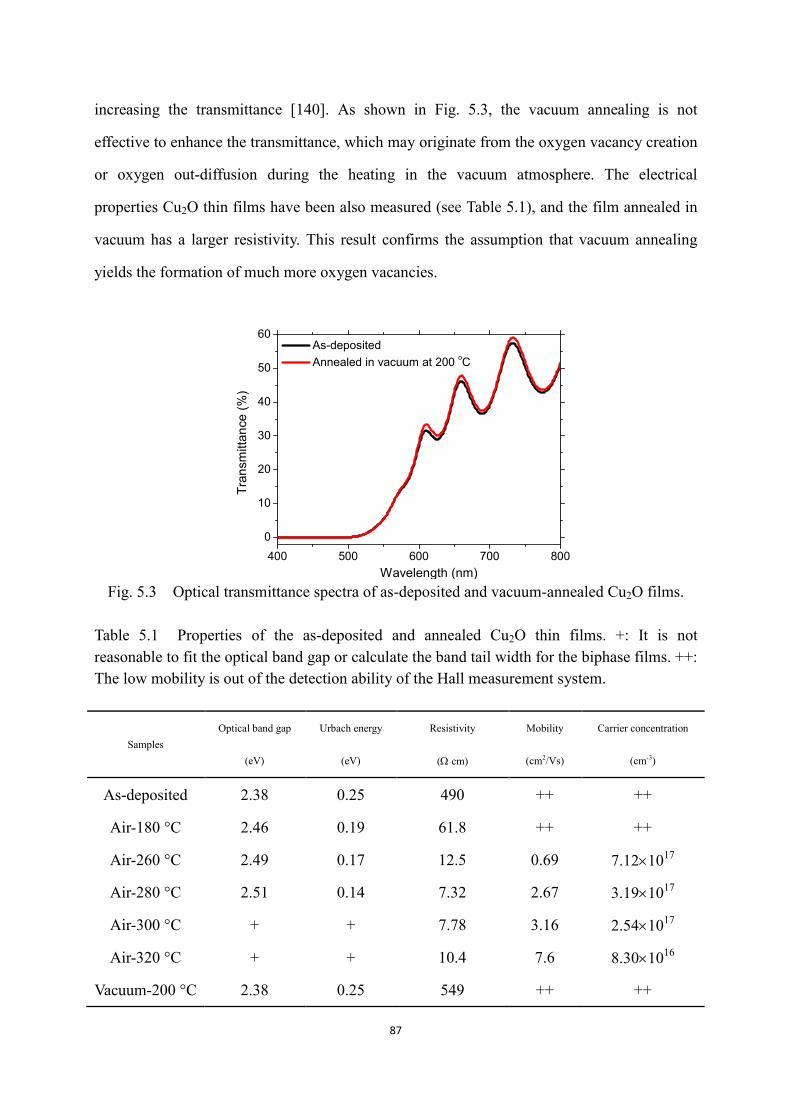
87
increasing the transmittance [140]. As shown in Fig. 5.3, the vacuum annealing is not
effective to enhance the transmittance, which may originate from the oxygen vacancy creation
or oxygen out-diffusion during the heating in the vacuum atmosphere. The electrical
properties Cu2O thin films have been also measured (see Table 5.1), and the film annealed in
vacuum has a larger resistivity. This result confirms the assumption that vacuum annealing
yields the formation of much more oxygen vacancies.
400 500 600 700 800
0
10
20
30
40
50
60
Tran
smitt
ance
(%)
Wavelength (nm)
As-deposited Annealed in vacuum at 200 oC
Fig. 5.3 Optical transmittance spectra of as-deposited and vacuum-annealed Cu2O films.
Table 5.1 Properties of the as-deposited and annealed Cu2O thin films. +: It is not reasonable to fit the optical band gap or calculate the band tail width for the biphase films. ++: The low mobility is out of the detection ability of the Hall measurement system.
Samples Optical band gap
(eV)
Urbach energy
(eV)
Resistivity
( cm)
Mobility
(cm2/Vs)
Carrier concentration
(cm-3)
As-deposited 2.38 0.25 490 ++ ++
Air-180 °C 2.46 0.19 61.8 ++ ++
Air-260 °C 2.49 0.17 12.5 0.69 7.121017
Air-280 °C 2.51 0.14 7.32 2.67 3.191017
Air-300 °C + + 7.78 3.16 2.541017
Air-320 °C + + 10.4 7.6 8.301016
Vacuum-200 °C 2.38 0.25 549 ++ ++
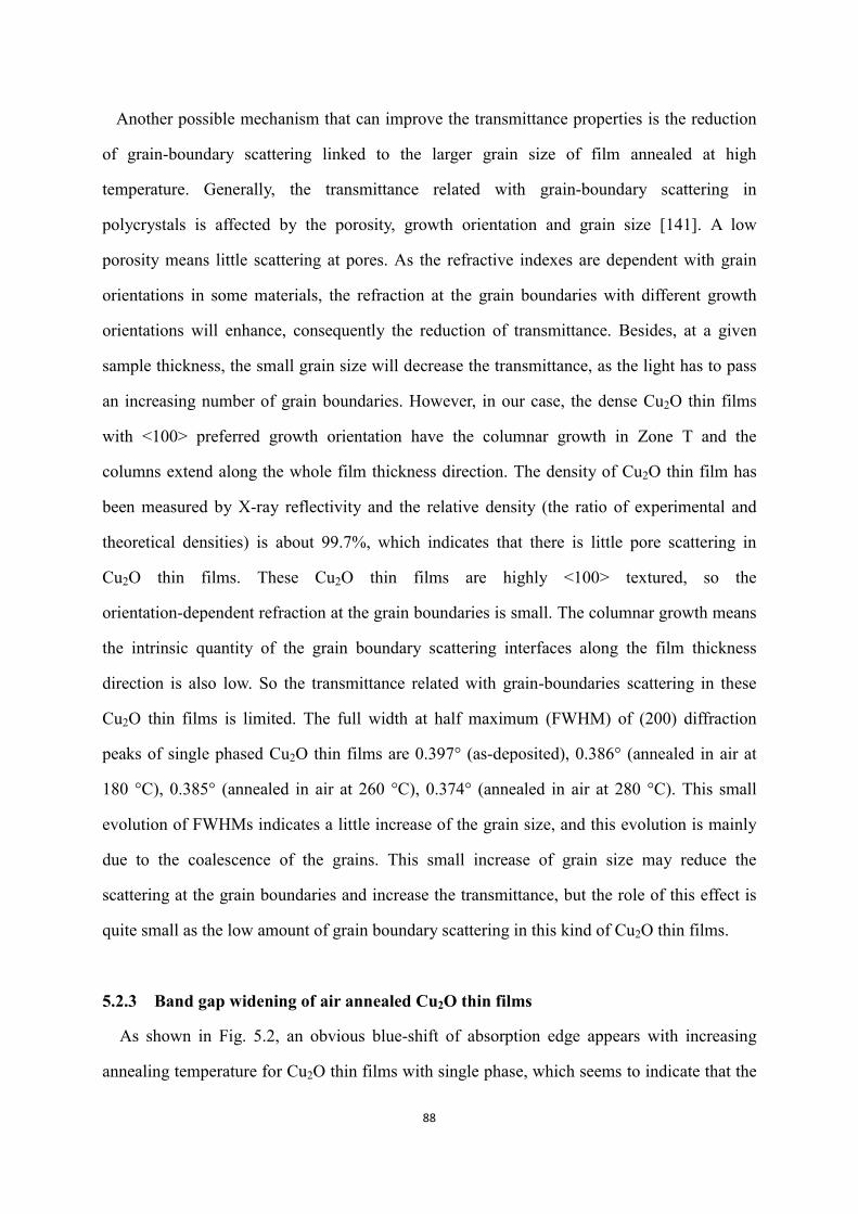
88
Another possible mechanism that can improve the transmittance properties is the reduction
of grain-boundary scattering linked to the larger grain size of film annealed at high
temperature. Generally, the transmittance related with grain-boundary scattering in
polycrystals is affected by the porosity, growth orientation and grain size [141]. A low
porosity means little scattering at pores. As the refractive indexes are dependent with grain
orientations in some materials, the refraction at the grain boundaries with different growth
orientations will enhance, consequently the reduction of transmittance. Besides, at a given
sample thickness, the small grain size will decrease the transmittance, as the light has to pass
an increasing number of grain boundaries. However, in our case, the dense Cu2O thin films
with <100> preferred growth orientation have the columnar growth in Zone T and the
columns extend along the whole film thickness direction. The density of Cu2O thin film has
been measured by X-ray reflectivity and the relative density (the ratio of experimental and
theoretical densities) is about 99.7%, which indicates that there is little pore scattering in
Cu2O thin films. These Cu2O thin films are highly <100> textured, so the
orientation-dependent refraction at the grain boundaries is small. The columnar growth means
the intrinsic quantity of the grain boundary scattering interfaces along the film thickness
direction is also low. So the transmittance related with grain-boundaries scattering in these
Cu2O thin films is limited. The full width at half maximum (FWHM) of (200) diffraction
peaks of single phased Cu2O thin films are 0.397° (as-deposited), 0.386° (annealed in air at
180 °C), 0.385° (annealed in air at 260 °C), 0.374° (annealed in air at 280 °C). This small
evolution of FWHMs indicates a little increase of the grain size, and this evolution is mainly
due to the coalescence of the grains. This small increase of grain size may reduce the
scattering at the grain boundaries and increase the transmittance, but the role of this effect is
quite small as the low amount of grain boundary scattering in this kind of Cu2O thin films.
5.2.3 Band gap widening of air annealed Cu2O thin films
As shown in Fig. 5.2, an obvious blue-shift of absorption edge appears with increasing
annealing temperature for Cu2O thin films with single phase, which seems to indicate that the
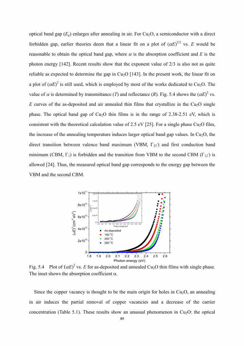
89
optical band gap (Eg) enlarges after annealing in air. For Cu2O, a semiconductor with a direct
forbidden gap, earlier theories deem that a linear fit on a plot of (E)2/3 vs. E would be
reasonable to obtain the optical band gap, where is the absorption coefficient and E is the
photon energy [142]. Recent results show that the exponent value of 2/3 is also not as quite
reliable as expected to determine the gap in Cu2O [143]. In the present work, the linear fit on
a plot of (E)2 is still used, which is employed by most of the works dedicated to Cu2O. The
value of is determined by transmittance (T) and reflectance (R). Fig. 5.4 shows the (E)2 vs.
E curves of the as-deposited and air annealed thin films that crystallize in the Cu2O single
phase. The optical band gap of Cu2O thin films is in the range of 2.38-2.51 eV, which is
consistent with the theoretical calculation value of 2.5 eV [25]. For a single phase Cu2O film,
the increase of the annealing temperature induces larger optical band gap values. In Cu2O, the
direct transition between valence band maximum (VBM, 25,) and first conduction band
minimum (CBM, 1) is forbidden and the transition from VBM to the second CBM (12,) is
allowed [24]. Thus, the measured optical band gap corresponds to the energy gap between the
VBM and the second CBM.
1.8 1.9 2.0 2.1 2.2 2.3 2.4 2.5 2.60
2x10¹⁰
4x10¹⁰
6x10¹⁰
8x10¹⁰
1x10¹¹
As-deposited 180 oC 260 oC 280 oC
( E
)2 (c
m-2
eV2 )
Photon energy (eV)
1.5 1.6 1.7 1.8 1.9 2.0 2.1 2.2 2.3 2.4 2.5 2.60.0
4.0x10⁴
8.0x10⁴
1.2x10⁵
1.6x10⁵
(c
m-1)
Photon energy (eV)
Fig. 5.4 Plot of (E)2 vs. E for as-deposited and annealed Cu2O thin films with single phase. The inset shows the absorption coefficient
Since the copper vacancy is thought to be the main origin for holes in Cu2O, an annealing
in air induces the partial removal of copper vacancies and a decrease of the carrier
concentration (Table 5.1). These results show an unusual phenomenon in Cu2O: the optical

90
band gap becomes wide while the carrier concentration decreases. The absorption coefficient
(shown in the inset of Fig.5.4), obtained in this study or reported by Malerba et al. [143],
always shows a non-zero value below the gap, indicating the presence of subgap absorption in
Cu2O thin films. Therefore, one of the possible mechanisms for the optical band gap widening
is that the merging of defect states and bands produce band tails and, the thermal annealing in
air can relieve part of the band tails. Based on this, the assumed schematic band structures of
the as-deposited and air annealed films are shown in Fig. 5.5. For the as-deposited thin films,
the defect levels with large density of states merge with each other to engender the defect
band that is also expected to merge with the valence band to form a band tail, yielding a
narrowing of the optical band gap (see Fig. 5.5(a)). After thermal annealing in air, parts of the
defects are removed or suppressed, resulting in an enlargement of the measured optical band
gap (see Fig. 5.5(b)). As shown in the inset of Fig. 5.4, it appears that the subgap absorption
of Cu2O thin film annealed at 280 °C is still large, which demonstrates the defect states are
still of high density. In order to verify this assumption, the Urbach energy (Eu), which
describes the width of the absorption tail, has been calculated using a linear portion of
ln(E)below the optical band gap using the following expression [144] = ( ) (5-1)
The Urbach energy of single phased Cu2O thin films is presented in Table 5.1, which clearly
shows that the optical band gap increases with decreasing Urbach energy. These results
support our argument that the optical band gap widening of air annealed Cu2O thin films
could be due to the reduction of the band tail.
Since the Cu2O film annealed in air at 280 oC has less defect states than other single phased
thin films, its optical band gap should be much more close to the ideal value. Considering that
the energy difference between the first CBM and the second CBM is 0.45 ~ 0.51 eV, [24],
[53], [55], [145], the room temperature band gap between VBM and the first CBM is
estimated to be 2.00 ~ 2.06 eV, which agrees well with the theoretical calculation value of
2.03 eV [25].

91
Fig. 5.5 The assumed schematic band structures of as-deposited (a) and air annealed (b) Cu2O thin films.
5.2.4 Photoluminesence analyses on Cu2O thin films
The defect information obtained by previous photoluminescence (PL) measurements in
Cu2O is controversial with recent first-principle calculations. Therefore the PL spectra of
Cu2O thin films have been measured to make a preliminary discussion combining
experimental results with recent calculations. Fig. 5.6 shows the PL spectra of as-deposited
and annealed Cu2O thin films on glass substrates measured at 5 K. Several wide peaks have
been observed above 2 eV. The peak near 3.1 eV (E()) is the recombination of the
interband transition between and points [25], [55]. The peak at about 2.3 eV (EG) is
related with green exciton, while 2.18 eV (2pEY) and 2.02 eV (1sEY) peaks are 2p and 1s
yellow excitons, respectively [54], [55]. The sharp peak at about 1.9 eV is the second order of
the laser beam. The peak near 1.7 eV is a defect peak, but its origin is still debated. Previous
experimental results showed that this peak can be due to the recombination of exciton bound
to double charged oxygen vacancy ( 2OV )[8], [53]–[55]. These authors also claim that there are
two other peaks at about 1.35 eV and 1.53 eV related with copper vacancy ( CuV ) and single
charged oxygen vacancy ( OV ), respectively. However, recent theoretical results obtained by
several groups using different calculation methods tend to show that the oxygen vacancy in
Cu2O is only stable in the neutral ( OV ) state [42], [44], [56]. The calculation results make
sense as they can explain the impossibility to realize n-type Cu2O. Provided that the single or
double positive charged oxygen vacancy indeed exists in Cu2O with high density, it will be
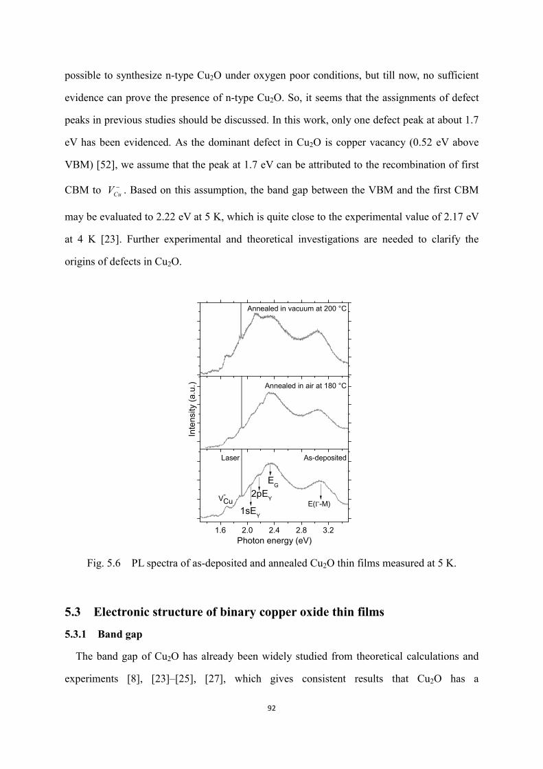
92
possible to synthesize n-type Cu2O under oxygen poor conditions, but till now, no sufficient
evidence can prove the presence of n-type Cu2O. So, it seems that the assignments of defect
peaks in previous studies should be discussed. In this work, only one defect peak at about 1.7
eV has been evidenced. As the dominant defect in Cu2O is copper vacancy (0.52 eV above
VBM) [52], we assume that the peak at 1.7 eV can be attributed to the recombination of first
CBM to CuV . Based on this assumption, the band gap between the VBM and the first CBM
may be evaluated to 2.22 eV at 5 K, which is quite close to the experimental value of 2.17 eV
at 4 K [23]. Further experimental and theoretical investigations are needed to clarify the
origins of defects in Cu2O.
1.6 2.0 2.4 2.8 3.2
Laser
V-Cu
1sEY
2pEY
EG
E(-M)
As-deposited
Photon energy (eV)
Annealed in air at 180 °C
Inte
nsity
(a.u
.)
Annealed in vacuum at 200 °C
Fig. 5.6 PL spectra of as-deposited and annealed Cu2O thin films measured at 5 K.
5.3 Electronic structure of binary copper oxide thin films
5.3.1 Band gap
The band gap of Cu2O has already been widely studied from theoretical calculations and
experiments [8], [23]–[25], [27], which gives consistent results that Cu2O has a

93
direct-forbidden gap of about 2 eV and a direct optical band gap of approx. 2.5-2.7 eV, as
shown in Table 5.2.
Table 5.2 The band gap energies (in eV) of Cu2O, Cu4O3 and CuO obtained from GWLF + Vd calculations and experiments. The direct (d) or indirect (i) nature of the gap ( gE ) has been noted. absE is the absorption threshold energy for direct and allowed optical transitions, which is determined from the calculated absorption coefficient somewhat arbitrarily at cm-1. *
absE is the experimental optical absorption threshold energy, which is identified from the first-order derivation.
GWLF + Vd cal. Exp.
gE absE *
absE
Cu2O 2.03 (d) [24] 2.7 (d) [24] 2.5 [27]
Cu4O3 0.84 (i) 1.59 (d) 1.37
CuO 1.2 (i) 1.48 (d) 1.5
Fig. 5.7 shows the absorption coefficient () of Cu4O3 attained by optical measurements
and GW calculation here, as well as by ellipsometry (Meyer et al. [8]). The calculation
predicts an indirect band gap of 0.84 eV and a direct band gap of 1.59 eV, whereas the
absorption becomes appreciable only at photon energies 1.59 eV (see Fig. 5.7 and Table 5.2).
Checking the details of experimental optical absorption spectrum from transmittance and
reflectance measurements in Fig. 5.7, it is found that the spectrum can be divided into two
parts, as the red dash lines marked: when the photon energy is larger than 1.37 eV, the
absorption coefficient increases sharply with increasing photon energy; below 1.37 eV, the
absorption has a tendency to increase, even though there is an interference effect. This
experimental absorption spectrum indicates that the optical absorption threshold energy is
about 1.37 eV, which is consistent with the theoretical value of 1.59 eV. To be pointed out
here, all the calculations here are done for the low temperature antiferromagnetic
configurations without the consideration of defects, grain boundaries and magnetic
fluctuations, which may affect the optical absorption. However, this behavior is not observed
in Cu4O3 thin films by Meyer et al. using ellipsometry [8], which may be due to the

94
elimination of detailed information by the complicated fitting in ellipsometry measurements.
0,6 0,8 1,0 1,2 1,4 1,6 1,8 2,0 2,2
Exp. by T and R GWLF+Vd cal. Ellipsometry by Meyer et al
Photon energy (eV)
Abs
orpt
ion
(cm
-1)
Fig. 5.7 Optical absorption coefficient of Cu4O3. The absorption spectrum by ellipsometry is attained from Ref. [8].
The origin of two absorption regions in experimental spectrum remains ambiguous and it
could come from a variety of factors. One possible source is the phonon assisted transitions
with low intensity. As the indirect band gap of 0.84 eV predicted by the GWLF + Vd calculation
is much lower than the direct transition of 1.59 eV, the phonon assisted transitions at room
temperature may lead to sub-gap absorption. On the other hand, the d-d and/or s-d excitations,
or excitons, could also form sub-gap absorption, even though they have not been reported in
copper oxides. Besides, the defect band tail originated the merging of defects may play a limit
role for this sub-gap absorption. The defect band tail in Cu2O has been clearly identified by
the analyses of sub-gap absorption (see Fig. 5.5), which is also detected by UPS spectrum
with the non-zero states close to Fermi level, e.g., in the energy range of -0.2 − 0 eV, as shown
in Fig. 5.8. However, such non-zero state in the energy range of -0.1 − 0 eV is not notable in
Cu4O3 thin film, indicating less valence band tail than that in Cu2O thin films. In addition, the
rough estimation of Urbach energy 0.77 eV (equal to 56% of the optical absorption threshold
energy) contradicts to the well crystallization of Cu4O3 thin films, which also demonstrates
the limit role of defect band tail. Indeed, the plural mechanisms may make joint contributions
to the sub-gap absorption, leading to the difficulty to discuss them seperatedly. It should be
noted that we do not care the absolute value of experimental absorption coefficient in low
photon energy range, as the interference effect, the noise of UV-Vis-NIR spectrometer and the
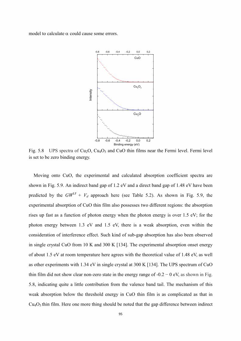
95
model to calculate could cause some errors.
-0,8 -0,6 -0,4 -0,2 0,0 0,2
-0,8 -0,6 -0,4 -0,2 0,0 0,2
Binding energy (eV)
Cu2O
Inte
nsity
Cu4O3
CuO
Fig. 5.8 UPS spectra of Cu2O, Cu4O3 and CuO thin films near the Fermi level. Fermi level is set to be zero binding energy.
Moving onto CuO, the experimental and calculated absorption coefficient spectra are
shown in Fig. 5.9. An indirect band gap of 1.2 eV and a direct band gap of 1.48 eV have been
predicted by the GWLF + Vd approach here (see Table 5.2). As shown in Fig. 5.9, the
experimental absorption of CuO thin film also possesses two different regions: the absorption
rises up fast as a function of photon energy when the photon energy is over 1.5 eV; for the
photon energy between 1.3 eV and 1.5 eV, there is a weak absorption, even within the
consideration of interference effect. Such kind of sub-gap absorption has also been observed
in single crystal CuO from 10 K and 300 K [134]. The experimental absorption onset energy
of about 1.5 eV at room temperature here agrees with the theoretical value of 1.48 eV, as well
as other experiments with 1.34 eV in single crystal at 300 K [134]. The UPS spectrum of CuO
thin film did not show clear non-zero state in the energy range of -0.2 − 0 eV, as shown in Fig.
5.8, indicating quite a little contribution from the valence band tail. The mechanism of this
weak absorption below the threshold energy in CuO thin film is as complicated as that in
Cu4O3 thin film. Here one more thing should be noted that the gap difference between indirect
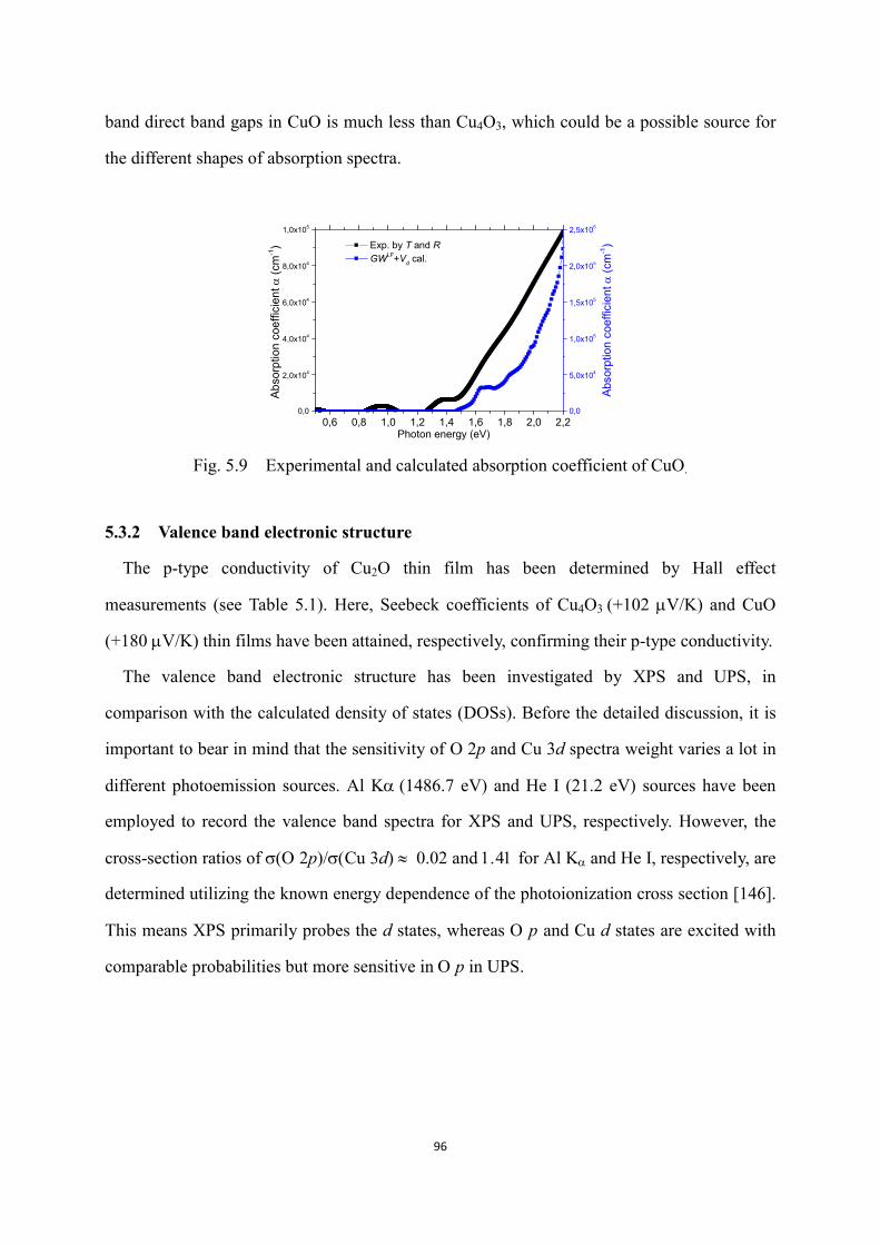
96
band direct band gaps in CuO is much less than Cu4O3, which could be a possible source for
the different shapes of absorption spectra.
0,6 0,8 1,0 1,2 1,4 1,6 1,8 2,0 2,20,0
2,0x10⁴
4,0x10⁴
6,0x10⁴
8,0x10⁴
1,0x10⁵
Exp. by T and R GWLF+Vd cal.
Photon energy (eV)
Abso
rptio
n co
effic
ient
(c
m-1)
0,0
5,0x10⁴
1,0x10⁵
1,5x10⁵
2,0x10⁵
2,5x10⁵
Abs
orpt
ion
coef
ficie
nt (c
m-1)
Fig. 5.9 Experimental and calculated absorption coefficient of CuO.
5.3.2 Valence band electronic structure
The p-type conductivity of Cu2O thin film has been determined by Hall effect
measurements (see Table 5.1). Here, Seebeck coefficients of Cu4O3 (+102 V/K) and CuO
(+180 V/K) thin films have been attained, respectively, confirming their p-type conductivity.
The valence band electronic structure has been investigated by XPS and UPS, in
comparison with the calculated density of states (DOSs). Before the detailed discussion, it is
important to bear in mind that the sensitivity of O 2p and Cu 3d spectra weight varies a lot in
different photoemission sources. Al K(1486.7 eV) and He I (21.2 eV) sources have been
employed to record the valence band spectra for XPS and UPS, respectively. However, the
cross-section ratios of (2p)(Cu 3d)0.02 and for Al Kand He I, respectively, are
determined utilizing the known energy dependence of the photoionization cross section [146].
This means XPS primarily probes the d states, whereas p and Cu d states are excited with
comparable probabilities but more sensitive in p in UPS.

97
-8 -7 -6 -5 -4 -3 -2 -1 0
-8 -7 -6 -5 -4 -3 -2 -1 0
Inte
nsity
(a.u
.)
XPS
Energy (eV)
UPS
Cu d PDOS
O p PDOS
Total DOS
Fig. 5.10 Experimental valence band spectra and calculated DOSs of Cu2O. The VBM is set to zero. The theoretical total DOS (in black), O p (in red) and Cu d (in blue) PDOS are convoluted with a Gaussian broadening of 0.4 eV to mimic temperature and instrumental broadening effects. Besides, all DOSs have been normalized to integrate to unity over the valence band. UPS and XPS spectra are plotted in green and magenta, respectively.
The photoemission valence band spectra and the theoretical DOSs of Cu2O are shown in
Fig. 5.10. One can distinguish three energy regions from theoretical DOSs. Between -7 and -5
eV, it is dominated by O 2p character. Pronounced Cu 3d states are concentrated in the energy
range of -4 − -2 eV. While a hybridization between Cu 3d and O 2p with close intensity, is
spread from -2 to 0 eV. As shown in Fig. 5.10, the shape of total DOS is in accordance with
the UPS spectrum. Considering that the calculated DOS is k point integrated, whereas the
experimental curve is not [147], the overall agreement is fair. Meanwhile, in the energy range
of -4 − 0 eV, XPS result shows good consistency with UPS spectra, theoretical total DOS and
Cu d PDOS. Such agreement between XPS and UPS may originate from the composition of
states in this energy region, where it is of notable Cu 3d character and only a little O 2p
contribution. Thus, the weakness of cross-section ratio in XPS or UPS is not a serious issue,
and they can give the similar results. This is not the same cases in Cu4O3 and CuO (we will
discuss later). Looking at the dominant O 2p character in the energy range of -7 − -5 eV, the
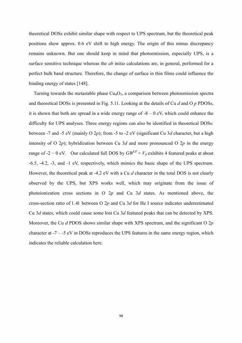
98
theoretical DOSs exhibit similar shape with respect to UPS spectrum, but the theoretical peak
positions show approx. 0.6 eV shift to high energy. The origin of this minus discrepancy
remains unknown. But one should keep in mind that photoemission, especially UPS, is a
surface sensitive technique whereas the ab initio calculations are, in general, performed for a
perfect bulk band structure. Therefore, the change of surface in thin films could influence the
binding energy of states [148].
Turning towards the metastable phase Cu4O3, a comparison between photoemission spectra
and theoretical DOSs is presented in Fig. 5.11. Looking at the details of Cu d and O p PDOSs,
it is shown that both are spread in a wide energy range of -8 – 0 eV, which could enhance the
difficulty for UPS analyses. Three energy regions can also be identified in theoretical DOSs:
between -7 and -5 eV (mainly O 2p); from -5 to -2 eV (significant Cu 3d character, but a high
intensity of O 2p); hybridization between Cu 3d and more pronounced O 2p in the energy
range of -2 − 0 eV. Our calculated full DOS by GWLF + Vd exhibits 4 featured peaks at about
-6.5, -4.2, -3, and -1 eV, respectively, which mimics the basic shape of the UPS spectrum.
However, the theoretical peak at -4.2 eV with a Cu d character in the total DOS is not clearly
observed by the UPS, but XPS works well, which may originate from the issue of
photoionization cross sections in O 2p and Cu 3d states. As mentioned above, the
cross-section ratio of between O 2p and Cu 3d for He I source indicates underestimated
Cu 3d states, which could cause some lost Cu 3d featured peaks that can be detected by XPS.
Moreover, the Cu d PDOS shows similar shape with XPS spectrum, and the significant O 2p
character at -7 – -5 eV in DOSs reproduces the UPS features in the same energy region, which
indicates the reliable calculation here.

99
-8 -7 -6 -5 -4 -3 -2 -1 0
-8 -7 -6 -5 -4 -3 -2 -1 0
Inte
nsity
(a.u
.)
Energy (eV)
XPS
UPS
Cu d PDOSO p PDOS
Total DOS
Fig. 5.11 Experimental valence band spectra and calculated DOSs of Cu4O3. The VBM is set to zero. The theoretical total DOS (in black), O p (in red) and Cu d (in blue) PDOS are convoluted with a Gaussian broadening of 0.4 eV to mimic temperature and instrumental broadening effects. Besides, all DOSs have been normalized to integrate to unity over the valence band. UPS and XPS spectra are plotted in green and magenta, respectively.
Moving onto CuO, our UPS spectrum here firstly is compared with other reported
experimental results, as shown in Fig. 5.12. For the spectrum obtained by Greiner et al. in
Ref.[149], it is an in-situ measurement from CuO thin films. Theoretically speaking, this kind
of in-situ measurement is reliable as there is no contamination or no etching. However, we
have also checked much more reported UPS or XPS valence band spectra of CuO from thin
films [130] or single crystal [150], and it is found that most of the valence band spectra show
the characteristics in Ref. [130] by Ghijsen et al. As shown in Fig. 5. 12, our UPS spectrum
has the almost the same peak positions with that in Ref. [130].

100
-8 -7 -6 -5 -4 -3 -2 -1 0
UPS He I by Ghijsen et al UPS He I Greiner et al UPS He I in this work
Binding energy (eV)
Inte
nsity
(a.u
.)
Fig. 5.12 Experimental UPS valence band spectra CuO. The other reported spectra are attained from Ref. [130] by Ghijsen et al and Ref. [149] by Greiner et al.
In Fig. 5.13, the experimental valence band spectra of CuO thin film are shown in
comparison to the theoretical DOSs calculated by GWLF + Vd approach. As similar as Cu4O3,
Cu d and O p PDOSs are also distributed in a wide energy range of -8 – 0 eV, and the total
DOSs can be divided into three regions. O 2p character is notable in the energy ranges of -7 –
-5 eV and -3 – 0 eV, while Cu 3d is concentrated in -5 – 3 eV. At first glance, the theoretical
total DOS and UPS spectrum show less satisfactory agreement, as the maximum peak at -4
eV with Cu d character in the total DOS contradicts to a valley in the UPS spectrum. Indeed,
the XPS with larger penetration depth and more Cu 3d sensitivity than UPS, succeeds to
detect this peak. Furthermore, the shape of Cu d PDOS is well consistent with the XPS
spectrum, indicating the fair agreement between photoemission spectra and theoretical DOSs.
Regarding the valley at about -4 eV in the UPS curve, this has also been observed in Ref. [150]
by Shen et al.. Shen et al. believed that this valley may come from the instability of CuO in
UHV, as the freshly cleaved CuO single crystal did not show clear valley.
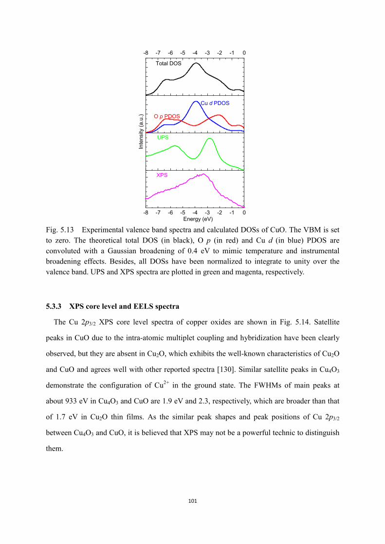
101
-8 -7 -6 -5 -4 -3 -2 -1 0
-8 -7 -6 -5 -4 -3 -2 -1 0
Inte
nsity
(a.u
.)
Energy (eV)
XPS
UPS
Cu d PDOS
O p PDOS
Total DOS
Fig. 5.13 Experimental valence band spectra and calculated DOSs of CuO. The VBM is set to zero. The theoretical total DOS (in black), O p (in red) and Cu d (in blue) PDOS are convoluted with a Gaussian broadening of 0.4 eV to mimic temperature and instrumental broadening effects. Besides, all DOSs have been normalized to integrate to unity over the valence band. UPS and XPS spectra are plotted in green and magenta, respectively.
5.3.3 XPS core level and EELS spectra
The Cu 2p3/2 XPS core level spectra of copper oxides are shown in Fig. 5.14. Satellite
peaks in CuO due to the intra-atomic multiplet coupling and hybridization have been clearly
observed, but they are absent in Cu2O, which exhibits the well-known characteristics of Cu2O
and CuO and agrees well with other reported spectra [130]. Similar satellite peaks in Cu4O3
demonstrate the configuration of Cu2+ in the ground state. The FWHMs of main peaks at
about 933 eV in Cu4O3 and CuO are 1.9 eV and 2.3, respectively, which are broader than that
of 1.7 eV in Cu2O thin films. As the similar peak shapes and peak positions of Cu 2p3/2
between Cu4O3 and CuO, it is believed that XPS may not be a powerful technic to distinguish
them.

102
4,0x10⁵
8,0x10⁵
1,2x10⁶
1,6x10⁶
2,0x10⁶
2,4x10⁶
925930935940945
Inte
nsity
Binding energy (eV)
Cu2O
Cu4O
3
CuO
Satellite peaks
Cu 2p3/2
950
Fig. 5.14 Cu 2p3/2 core-level XPS spectra of Cu2O, Cu4O3 and CuO thin films.
In order to study the electronic structures of copper oxides deeply, the EELS with the
characteristic of transmission electrons is employed, superior to the surface sensitive
photoemission spectroscopy. Energy loss near edge structure (ELNES) spectra of Cu L2,3 and
O K edges have been recorded, as shown in Fig. 5.15(a) and (b), respectively. The spectra
shape and the relative position of Cu L2,3 edges in CuO and Cu2O, particular the substructure
configurations (denoted as * in Fig. 5.15) in Cu2O, are in excellent agreements with previous
reports by X-ray absorption spectroscopy (XAS) [133], [136], [151], indicating the good
resolution and precision of ELNES in this work. As seen in Fig. 5.15(a), strong and sharp L2,3
white lines have been observed in Cu2O, which is in contrast to the traditional simple ionic
model. The dipole selection rules allow transitions from the 2p level into final states of s (∆l =
-1) or d (∆l = +1) character, but the ∆l = -1 channel is extremely low and it can be safely
ignored in a first approximation [131]. Hence, the presence of L edges white lines in EELS or
XAS requires the unfilled d shell. However, the traditional simple ionic model treats Cu1+ as a
3d10 cation with a full d shell, consequently there should be no L edges white lines in Cu2O.
However, there is no doubt that the sharp Cu L2,3 white lines in Cu2O can always be measured
by EELS or XAS [131], [133], [136], [151]. The origin of this kind of ‘unfilled’ 3d shell in
Cu2O remains controversial. One hypothesis assumes that the 3d shell of metallic Cu just has
9.6 electrons, and there is only 9.5 electrons in 3d orbital of Cu2O [152], [153]. Since this
assumption employs the questionable white lines in metallic Cu, we believe that this
hypothesis may require to be reconsidered carefully. Another one deems that the pronounced

103
on-site Cu 3d-4s hybridization in Cu2O will produce significant unoccupied 4s states in the
conduction band [136]. On the contrary, one hypothesis supposes that the empty 3d shell
originates from the hybridization of dz2 and higher-energy unoccupied 4s, which makes the dz
2
unoccupied [154]. From the viewpoint of charge density, 0.22 electrons per atom are removed
from dz2 states due to the hybridization [154], leading to the unfilled d shell. GWLF + Vd
calculations also predict an unusual Cu dz2-s hybridization and a strong Cu 3d contribution to
the conduction band, as Cu-dz2 and Cu-s orbitals share a common point group representation
(see Ref. [24]).
920 930 940 950 960 970 980
Inte
nsity
(a.u
.)
Energy loss (eV)
*
CuO
Cu4O3
L2
Cu1+
Cu2+L3
(a)
Cu2O
*
525 530 535 540 545 550 555 560
*
Cu4O3
CuO
Cu2O
Inte
nsity
(a.u
.)
Energy loss (eV)
(b)
*
Fig. 5.15 (a) Cu L2,3 edges (b) O K edge ELNES spectra of Cu2O, Cu4O3 and CuO, normalized to the peak height.
Checking the peak positions of Cu L2,3 white lines in Cu2O and CuO (see Fig. 5.15(a)), it is
revealed that the positions of Cu L2,3 edges are shift to lower energy loss for the higher
oxidation state. This contradicts the trends in Mn, V and Fe oxides that the energy loss moves
to higher energy for the higher oxidation state [155]. Employing the Cu L3 edges of Cu2O and
CuO as references, the white lines of Cu4O3 can be identified easily, where the strongest peak
with the energy loss of 931.1 eV and the shake-up peak at 933.7 eV correspond to Cu2+ and
Cu1+, respectively, as shown in Fig. 5.15(a). Similar situation exists in L2 edge. Concerning
the O K edges, these three phases exhibit significant discrepancies, as shown in Fig. 5.15(b).
Cu2O shows a prominent peak at 532.5 eV and minor features at higher energy loss. In the
case of Cu4O3, four peaks located at about 530.5, 533.4, 536 and 541 eV can be determined.

104
While four notable peaks with energy loss of 528.4, 532.9, 537.4, and 541 eV, are observed in
CuO. Utilizing the peaks with maximum intensities at about 532 − 533 eV as references, the
existence of pre-peaks with lower energy loss, as well as their relative energy shifts, could be
good indicators to distinguish these phases.
5.3.4 Conduction band electronic structure
In ELNES, L3 edge means 2p3/2 electrons are ejected to unoccupied d states above Fermi
level, while O K edge represents 1 s electrons are ejected to empty p states, within the
consideration of parities between initial and final states. Then, it is interesting to perform the
comparisons between experimental Cu L3 ELNES spectrum and theoretical empty Cu d states
in the conduction band, together with O K edge and O p states. Fig. 5.16 clearly shows that
the theoretical empty states calculated by GWLF + Vd do so well for the experimental ELNES
spectra in Cu and O of Cu2O, including the basic shape, the relative position and substructure
configuration. Similar comparisons in Cu4O3 also exhibit well consistency (see Fig. 5.17). It
is worth noting that the Cu d and O p PDOSs in the conduction band of Cu4O3 calculated by
LDA+U do not show so much accordance with the experiments. The comparisons of CuO are
shown in Fig. 5.18, which demonstrates that most of the experimental features are well
reproduced by the theory. Here, it is worth noting that some minus disagreement seems to
exist in these comparisons, e.g. the peak at about 4 eV in O K edge of Cu4O3 has a shift with
theoretical position (see Fig. 5.17(b)), or the peak at 6 eV in Cu d PDOS of CuO is not clearly
observed in the experiments (see Fig. 5.18(a)). But we still believe that the GWLF + Vd
calculation can describe the conduction band fairly, as most of experimental features are
predicted by the theory. One possible source for this disagreement is the neglecting s state in
the comparison between Cu L3 edge and Cu d PDOS. Usually, we only consider the ejected 2p
electrons move onto empty d states, as we did in this work. Actually, they can also move onto
empty s state with very low density. When we talk about the while lines (sharp peaks), we do
not consider the s state. But for the substructure peaks, s state may make contribution.
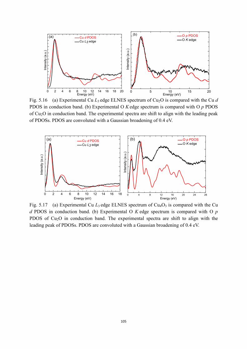
105
0 2 4 6 8 10 12 14 16 18 20
Cu d PDOS Cu L3 edge
Energy (eV)
Inte
nsity
(a.u
.)
(a)
0 5 10 15 20
O p PDOS O K edge
Energy (eV)
Inte
nsity
(a.u
.)
(b)
Fig. 5.16 (a) Experimental Cu L3 edge ELNES spectrum of Cu2O is compared with the Cu d PDOS in conduction band. (b) Experimental O K edge spectrum is compared with O p PDOS of Cu2O in conduction band. The experimental spectra are shift to align with the leading peak of PDOSs. PDOS are convoluted with a Gaussian broadening of 0.4 eV.
0 2 4 6 8 10 12 14 16 18
Cu d PDOS Cu L3 edge
Energy (eV)
Inte
nsity
(a.u
.)
(a)
0 4 8 12 16 20 24 28
O p PDOS O K edge
Energy (eV)
Inte
nsity
(a.u
.)
(b)
Fig. 5.17 (a) Experimental Cu L3 edge ELNES spectrum of Cu4O3 is compared with the Cu d PDOS in conduction band. (b) Experimental O K edge spectrum is compared with O p PDOS of Cu2O in conduction band. The experimental spectra are shift to align with the leading peak of PDOSs. PDOS are convoluted with a Gaussian broadening of 0.4 eV.
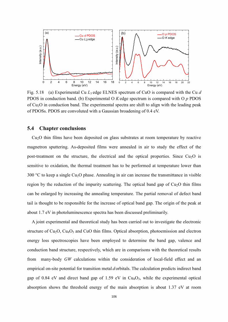
106
0 2 4 6 8 10 12 14 16 18
Cu d PDOS Cu L3 edge
Energy (eV)
Inte
nsity
(a.u
.)
(a)
0 2 4 6 8 10 12 14 16 18 20 22
O p PDOS O K edge
Energy (eV)
Inte
nsity
(a.u
.)
(b)
Fig. 5.18 (a) Experimental Cu L3 edge ELNES spectrum of CuO is compared with the Cu d PDOS in conduction band. (b) Experimental O K edge spectrum is compared with O p PDOS of Cu2O in conduction band. The experimental spectra are shift to align with the leading peak of PDOSs. PDOS are convoluted with a Gaussian broadening of 0.4 eV.
5.4 Chapter conclusions
Cu2O thin films have been deposited on glass substrates at room temperature by reactive
magnetron sputtering. As-deposited films were annealed in air to study the effect of the
post-treatment on the structure, the electrical and the optical properties. Since Cu2O is
sensitive to oxidation, the thermal treatment has to be performed at temperature lower than
300 °C to keep a single Cu2O phase. Annealing in air can increase the transmittance in visible
region by the reduction of the impurity scattering. The optical band gap of Cu2O thin films
can be enlarged by increasing the annealing temperature. The partial removal of defect band
tail is thought to be responsible for the increase of optical band gap. The origin of the peak at
about 1.7 eV in photoluminescence spectra has been discussed preliminarily.
A joint experimental and theoretical study has been carried out to investigate the electronic
structure of Cu2O, Cu4O3 and CuO thin films. Optical absorption, photoemission and electron
energy loss spectroscopies have been employed to determine the band gap, valence and
conduction band structure, respectively, which are in comparisons with the theoretical results
from many-body GW calculations within the consideration of local-field effect and an
empirical on-site potential for transition metal d orbitals. The calculation predicts indirect band
gap of 0.84 eV and direct band gap of 1.59 eV in Cu4O3, while the experimental optical
absorption shows the threshold energy of the main absorption is about 1.37 eV at room
107
temperature and a sub-absorption exists below this threshold energy. In the case of CuO,
theoretical calculation indicates an indirect band gap of 1.2 eV and a direct band gap of 1.48
eV, while a threshold energy of main absorption at about 1.5 eV is determined by optical
absorption spectrum at room temperature and a weak sub-absorption is observed below this
onset. Electron energy loss spectroscopy shows significant advance over X-ray photoemission
spectroscopy to distinguish these three phases. Meanwhile, the partial density of states in
conduction band measured by electron energy loss spectroscopy are fairly reproduced by the
calculation. X-ray and ultraviolet photoemission spectroscopies have been combined together
to study the valence band structure, while the experimental results show good consistency
with the theoretical electronic structure. Therefore, the overall agreement between
experimentally and theoretically determined band gap, valence and conduction band
electronic structure, is remarkably satisfactory, which seems to indicate that this kind of GW
scheme within the consideration of local-field effect and an empirical on-site potential for
transition metal d orbitals has the potential to be universal method for electronic structure
calculation. We hope that this work will stimulate further theoretical and experimental
advances.

108
109
Conclusions and outlook
Binary copper oxide (Cu2O, Cu4O3 and CuO) thin films have been selectively deposited on
glass and silicon substrates by magnetron sputtering at room temperature from a metallic
copper target in various Ar-O2 reactive mixtures. A schematic deposition diagram, which
describes the film structure as a function of O2 flow rate and total pressure, is depicted by
combining X-ray diffraction and Raman spectrometry. The oxygen flow rate process windows
for Cu2O or Cu4O3 single phase synthesis are narrow, while that for CuO is wider. Increasing
the total pressure, the oxygen process windows to synthesize single phase Cu2O and Cu4O3
have a tendency to become narrow, while the required oxygen flow rates are shifted to lower
values. Between each single phase domain, the films are biphase: either Cu2O + Cu4O3 or
Cu4O3 + CuO. It is found that the deposition total pressure is a relevant parameter to control
the texture and the morphology of pure Cu2O and Cu4O3 films. Low total pressure favours the
growth of planes with high surface energy ((100) for Cu2O and (101) for Cu4O3) parallel to
the substrate. On the other hand, high total pressure facilitates the growth of planes with low
surface energy ((111) for Cu2O and (100) for Cu4O3). The oxygen flow rate is effective to
control the preferred orientation of CuO thin films that evolves from <111> to < 111
> with the
increase of oxygen flow rate.
Local homoepitaxial growth can be used to tune the growth orientations (<111> or <100>)
of Cu2O thin films on glass and silicon substrates. Using a two steps deposition procedure, a
highly textured Cu2O thin film with controlled orientation can be formed independently of the
deposition conditions. A Cu2O layer with preferred orientation acts as a continuous seed layer,
which determines the crystal orientation of the top layer grown even after air exposure and/or
without specific cleaning of the surface prior to deposition. High resolution transmission
electron microscopy analyses evidence that the columns of top layer epitaxially grown on

110
columns of seed layer, with the character of one column on one column. This kind of local
homoepitaxial growth can also be extended into tetragonal Cu4O3 thin films, but only to
produce the <100> texture. Besides, a local heteroepitaxial growth with the character of
several columns on one column has been observed in bilayer films of NiO on Cu2O. Using a
<111> oriented Cu2O seed layer, a NiO layer with highly <111> texture and good
crystallization can be formed, regardless of the intrinsic growth conditions of NiO.
An unusual microstructure has been evidenced in biphase Cu2O and Cu4O3 thin films,
where both phases have the vertically aligned columnar growth along the whole film
thickness direction. The local homoepitaxial growth behavior of Cu2O is thought to be
responsible for such a new microstructure. The intermediate oxygen flow rate between those
required to synthesize pure phase Cu2O and Cu4O3 induces the formation of some Cu2O
nucleus. Then the local homoepitaxial growth effect provides a strong driving force to grow
Cu2O columns along the whole film thickness from these nucleuses. Consequently, the two
phases (Cu2O and Cu4O3) grow separately and independently with vertically aligned
columnar microstructure. Such an unusual microstructure can also be extended to other
materials with certain requirements. Lower resistivity has been observed in this kind of
biphase thin films than single phase thin films, which may be due to the interface coupling
between Cu2O and Cu4O3 columns.
As-deposited Cu2O films exhibit high electrical resistivity and low optical transmittance.
To improve the film properties, post annealing treatments in air at various temperatures have
been performed. Since Cu2O is sensitive to oxidation, the thermal treatment has to be
performed at temperature lower than 300 °C to keep a single Cu2O phase. Annealing in air
can increase the transmittance in visible region by the reduction of the defect density.
Moreover, the optical band gap of Cu2O thin films is enlarged from 2.38 to 2.51 eV with
increasing annealing temperature. The increase of optical band gap accompanying the
reduction of Urbach energy indicates that the widening of optical band gap may result from
111
the partial elimination of defect band tail after thermal annealing in air. Photoluminescence
analyses have been performed on as-deposited and air annealed Cu2O films. Combining our
experimental results with recent reported calculations, the peak at about 1.7 eV in
photoluminescence spectra is assigned to the recombination of first conduction band
minimum to copper vacancy.
Finally, to bring relevant information about the electronic structure of copper oxides, a joint
experimental and theoretical study has been carried out. The calculated absorption threshold
energies for direct and allowed optical transitions agree well with optical absorption
experiments. Indirect band gaps with smaller values than the direct and allowed band gaps have
been predicted in Cu4O3 and CuO by calculations, which could be responsible for the
experimental sub-gap absorptions. Electron energy loss spectra of three phases exhibit
pronounced difference and it could be more powerful to distinguish them than surface
sensitive photoemission spectroscopies. Sharp L2,3 white lines have been observed in Cu2O,
which indicates the empty d states in the conduction band probably due to the hybridization.
The unoccupied partial density of states in conduction band probed by electron energy loss
spectroscopy are well reproduced by the GW calculation. X-ray and ultraviolet photoemission
spectroscopies have been combined together to study the valence band structure, while the
experimental spectra show good consistency with the theoretical electronic structure. Thus,
the overall agreement between experiments and calculations in band gap, valence and
conduction band electronic structure is remarkably good.
The work performed during this PhD opens future investigations. We list hereafter selected
points that are suitable for further studies:
In this thesis, the total sputtering pressure or oxygen flow rate can be used to tune the
preferred growth orientation of copper oxide thin films, but we only provide some
qualitative explanations. Further understanding of this tunable texture requires the
112
consideration of the concept of “energy per atom” and the ion bombardment effect by
plasma diagnostic and simulation.
Local homoepitaxial growth with characteristic of one column on one column can
promote the <100> texture in tetragonal Cu4O3 thin films, but it fails in the <101>
orientation. This kind of growth cannot be extended to monoclinic CuO thin films,
either. The origin of this behavior is still unknown. Thin films with larger column
width are needed to guarantee that the transmission electron microscopy sample
thickness is less than the column width. Then clear images at the interface between
two layers by high resolution transmission electron microscopy or scanning
transmission electron microscopy could be attained, which may provide useful
information on the atomic structure and chemistry of interface. Besides, in-situ
morphology measurements by atomic probe microscopy may provide the
understanding of nucleation in this local homoepitaxial growth.
Up to now, one series of thin film solar cells with the structure of
glass/Ni/Cu2O/ZnO/Al-ZnO (1.5 cm x 1.5 cm) has been prepared, but the efficiency is
only 0.083% (VOC = 35 mV, ISC = 0.047 mA, FF = 0.312). This weak efficiency may
originate from a variety of factors, such as surface recombination (Cu2O and ZnO are
not synthesized in the same deposition chamber), low mobility of Cu2O (substrate
holder is not heated), and poor metallic electrodes. In order to increase the efficiency,
more series of samples are required with special consideration on these negative
effects.
It is interesting to measure the optical absorption spectra of Cu4O3 and CuO thin films
at low temperature (liquid He), in order to suppress the phonon-assisted transitions,
which may provide useful information to assess the optical absorption characteristics.
Moreover, further experimental investigations on the electronic structure of strong
correlated CuO are required, such as measuring the valence band structure by a
synchrotron beamline with different photon energies.

113
Bibliography
[1] M. Moritz and M. Geszke-Moritz, “The newest achievements in synthesis, immobilization and practical applications of antibacterial nanoparticles,” Chem. Eng. J., vol. 228, pp. 596–613, 2013.
[2] P. E. D. Morgan, D. E. Partin, B. L. Chamberland, and M. O. Keeffe, “Synthesis of Paramelaconite : Cu4O3,” J. Solid State Chem., vol. 121, pp. 33–37, 1996.
[3] M. O’Keeffe and J. O. Bovin, “The crystal structure of paramelaconite, Cu4O3,” Am. Mineral., vol. 63, pp. 180–185, 1978.
[4] E. Fortunato, P. Barquinha, and R. Martins, “Oxide semiconductor thin-film transistors: A review of recent advances,” Adv. Mater., vol. 24, pp. 2945–2986, 2012.
[5] Q. Zhang, K. Zhang, D. Xu, G. Yang, H. Huang, F. Nie, C. Liu, and S. Yang, “CuO nanostructures: Synthesis, characterization, growth mechanisms, fundamental properties, and applications,” Prog. Mater. Sci., vol. 60, no. October 2013, pp. 208–237, 2014.
[6] B. Pecquenard, F. Le Cras, D. Poinot, O. Sicardy, and J. P. Manaud, “Thorough characterization of sputtered CuO thin films used as conversion material electrodes for lithium batteries,” ACS Appl. Mater. Interfaces, vol. 6, pp. 3413–3420, 2014.
[7] T. Minami, Y. Nishi, and T. Miyata, “Heterojunction solar cell with 6% efficiency based on an n-type aluminum–gallium–oxide thin film and p-type sodium-doped Cu2O sheet,” Appl. Phys. Express, vol. 8, p. 022301, 2015.
[8] B. K. Meyer, A. Polity, D. Reppin, M. Becker, P. Hering, P. J. Klar, T. Sander, C. Reindl, J. Benz, M. Eickhoff, C. Heiliger, M. Heinemann, J. Bläsing, A. Krost, S. Shokovets, C. Müller, and C. Ronning, “Binary copper oxide semiconductors: From materials towards devices,” Phys. Status Solidi B, vol. 249, no. 8, pp. 1487–1509, 2012.
[9] L. O. Grondahl, “The copper-cuprous-oxide rectifier and photoelectric cell,” Rev. Mod. Phys., vol. 5, p. 141, 1933.
[10] D. Samal, H. Tan, Y. Takamura, W. Siemons, J. Verbeeck, G. Van Tendeloo, E. Arenholz, C. A. Jenkins, G. Rijnders, and G. Koster, “Direct structural and spectroscopic investigation of ultrathin films of tetragonal CuO: Six-fold coordinated copper,” EPL (Europhysics Lett.), vol. 105, p. 17003, 2014.
[11] S. Moser, L. Moreschini, H.-Y. Yang, D. Innocenti, F. Fuchs, N. H. Hansen, Y. J. Chang, K. S. Kim, a. L. Walter, a. Bostwick, E. Rotenberg, F. Mila, and M. Grioni, “Angle-resolved photoemission spectroscopy of tetragonal CuO: Evidence for intralayer coupling between cupratelike sublattices,” Phys. Rev. Lett., vol. 113, no. October, p. 187001, 2014.
[12] JCPDS cards, “04-007-9767, 04-007-2184, 04-007-1375.”
114
[13] K. W. L.Schramm, G.Behr, W.Loser, “Thermodynamic reassessment of the Cu-O phase diagram,” J. Phase Equilibria Diffus., vol. 26, no. 6, pp. 605–612, 2005.
[14] K. J. Blobaum, D. Van Heerden, A. J. Wagner, D. H. Fairbrother, and T. P. Weihs, “Sputter-deposition and characterization of paramelaconite,” J. Mater. Res., vol. 18, no. 7, pp. 1535–1542, 2003.
[15] E. P. S. Tan, Y. Zhu, T. Yu, L. Dai, C. H. Sow, V. B. C. Tan, and C. T. Lim, “Crystallinity and surface effects on Young’s modulus of CuO nanowires,” Appl. Phys. Lett., vol. 90, p. 163112, 2007.
[16] G. Zhou and J. C. Yang, “Formation of quasi-one-dimensional Cu2O structures by in situ oxidation of Cu(100),” Phys. Rev. Lett., no. 89, p. 106101, 2002.
[17] W. Siemons, G. Koster, D. H. A. Blank, R. H. Hammond, T. H. Geballe, and M. R. Beasley, “Tetragonal CuO: End member of the 3d transition metal monoxides,” Phys. Rev. B, vol. 79, p. 195122, 2009.
[18] J. F. Pierson, C. Petitjean, and D. Horwat, “Structure control in reactively sputtered Ag/Cu/(Mn)/O films,” Plasma Process. Polym., vol. 6, pp. 393–400, 2009.
[19] L. Debbichi, M. C. Marco de Lucas, J. F. Pierson, and P. Kruger, “Vibrational properties of CuO and Cu4O3 from first-principles calculations, and Raman and infrared spectroscopy,” J. Phys. Chem. C, vol. 116, pp. 10232–10237, 2012.
[20] T. Sander, C. T. Reindl, M. Giar, B. Eifert, M. Heinemann, C. Heiliger, and P. J. Klar, “Correlation of intrinsic point defects and the Raman modes of cuprous oxide,” Phys. Rev. B, vol. 90, p. 045203, 2014.
[21] Y. Wang, J. Ghanbaja, F. Soldera, P. Boulet, D. Horwat, F. Mücklich, and J. F. Pierson, “Controlling the preferred orientation in sputter-deposited Cu2O thin films: Influence of the initial growth stage and homoepitaxial growth mechanism,” Acta Mater., vol. 76, pp. 207–212, 2014.
[22] Y. Wang, J. Ghanbaja, F. Soldera, S. Migot, P. Boulet, D. Horwat, F. Mücklich, and J. F. Pierson, “Tuning the structure and preferred orientation in reactively sputtered copper oxide thin films,” Appl. Surf. Sci., vol. 335, pp. 85–91, 2015.
[23] A. Jolk and C. F. Klingshirn, “Linear and nonlinear excitonic absorption and photoluminescence spectra in Cu2O: line shape analysis and exciton drift,” Phys. Status Solidi B, vol. 206, pp. 841–849, 1998.
[24] S. Lany, “Band-structure calculations for the 3d transition metal oxides in GW,” Phys. Rev. B, vol. 87, p. 085112, 2013.
[25] M. Heinemann, B. Eifert, and C. Heiliger, “Band structure and phase stability of the copper oxides Cu2O, CuO, and Cu4O3,” Phys. Rev. B, vol. 87, no. February, p. 115111, 2013.
[26] L. Y. Isseroff and E. a. Carter, “Importance of reference Hamiltonians containing exact exchange for accurate one-shot GW calculations of Cu2O,” Phys. Rev. B, vol. 85, p. 235142, 2012.

115
[27] Y. Wang, P. Miska, D. Pilloud, D. Horwat, F. Mücklich, and J. F. Pierson, “Transmittance enhancement and optical band gap widening of Cu2O thin films after air annealing,” J. Appl. Phys., vol. 115, p. 073505, 2014.
[28] L. Debbichi, M. C. Marco de Lucas, and P. Krüger, “Electronic structure, lattice dynamics and thermodynamic stability of paramelaconite Cu4O3,” Mater. Chem. Phys., vol. 148, no. 1–2, pp. 293–298, 2014.
[29] J. F. Pierson, A. Thobor-Keck, and A. Billard, “Cuprite, paramelaconite and tenorite films deposited by reactive magnetron sputtering,” Appl. Surf. Sci., vol. 210, pp. 359–367, 2003.
[30] P. K. Ooi, S. S. Ng, M. J. Abdullah, H. Abu Hassan, and Z. Hassan, “Effects of oxygen percentage on the growth of copper oxide thin films by reactive radio frequency sputtering,” Mater. Chem. Phys., vol. 140, pp. 243–248, 2013.
[31] J. F. Pierson, E. Duverger, and O. Banakh, “Experimental and theoretical contributions to the determination of optical properties of synthetic paramelaconite,” J. Solid State Chem., vol. 180, pp. 968–973, 2007.
[32] B. J. Hansen, N. Kouklin, G. Lu, I. K. Lin, J. Chen, and X. Zhang, “Transport, analyte detection, and opto-electronic response of p-type CuO nanowires,” J. Phys. Chem. C, vol. 114, pp. 2440–2447, 2010.
[33] C. E. Ekuma, V. I. Anisimov, and M. Jarrell, “Electronic structure and spectra of CuO,” Eur. Phys. J. B, vol. 87, p. 23, 2014.
[34] R. Claudia, F. Sottile, and L. Reining, “Quasiparticle excitations in the photoemission spectrum of CuO from first principles : a GW study,” Phys. Rev. B, vol. 91, p. 045102, 2015.
[35] K. S. Rabinovich, L. L. Samoilenko, a. S. Zhuravleva, and a. G. Shneider, “Magnetic properties of high-symmetry CuO,” Appl. Phys. Lett., vol. 104, p. 182406, 2014.
[36] J. G. Bednorz and K. A. Mller, “Perovskite-type oxides-The new approach to high-Tc superconductivity,” Rev. Mod. Phys., vol. 60, no. 3, pp. 585–600, 1988.
[37] X. Q. Chen, C. L. Fu, C. Franchini, and R. Podloucky, “Hybrid density-functional calculation of the electronic and magnetic structures of tetragonal CuO,” Phys. Rev. B, vol. 80, pp. 1–5, 2009.
[38] Y. S. Lee, M. T. Winkler, S. C. Siah, R. Brandt, and T. Buonassisi, “Hall mobility of cuprous oxide thin films deposited by reactive direct-current magnetron sputtering,” Appl. Phys. Lett., vol. 98, p. 192115, 2011.
[39] D. Muñoz-Rojas, M. Jordan, C. Yeoh, A. T. Marin, A. Kursumovic, L. A. Dunlop, D. C. Iza, A. Chen, H. Wang, and J. L. MacManus Driscoll, “Growth of ∼5 cm2V-1s-1 mobility, p-type Copper(I) oxide (Cu2O)
116
films by fast atmospheric atomic layer deposition (AALD) at 225°C and below,” AIP Adv., vol. 2, no. I, pp. 0–7, 2012.
[40] N. Naka, I. Akimoto, M. Shirai, and K. I. Kan’No, “Time-resolved cyclotron resonance in cuprous oxide,” Phys. Rev. B, vol. 85, p. 035209, 2012.
[41] D. O. Scanlon, B. J. Morgan, G. W. Watson, and A. Walsh, “Acceptor levels in p-type Cu2O: Rationalizing theory and Experiment,” Phys. Rev. Lett., vol. 103, p. 096405, 2009.
[42] A. Soon, X. Y. Cui, B. Delley, S. H. Wei, and C. Stampfl, “Native defect-induced multifarious magnetism in nonstoichiometric cuprous oxide: First-principles study of bulk and surface properties of Cu2O,” Phys. Rev. B, vol. 79, p. 035205, 2009.
[43] G. K. Paul, Y. Nawa, H. Sato, T. Sakurai, and K. Akimoto, “Defects in Cu2O studied by deep level transient spectroscopy,” Appl. Phys. Lett., vol. 88, p. 141901, 2006.
[44] D. O. Scanlon and G. W. Watson, “Uncovering the complex behavior of hydrogen in Cu2O,” Phys. Rev. Lett., vol. 106, no. May, p. 186403, 2011.
[45] D. Wu, Q. Zhang, and M. Tao, “LSDA + U study of cupric oxide : Electronic structure and native point defects,” Phys. Rev. B, vol. 73, p. 235206, 2006.
[46] Y. Peng, Z. Zhang, T. Viet Pham, Y. Zhao, P. Wu, and J. Wang, “Density functional theory analysis of dopants in cupric oxide,” J. Appl. Phys., vol. 111, p. 103708, 2012.
[47] C. M. McShane and K. S. Choi, “Photocurrent enhancement of n-type Cu2O electrodes achieved by controlling dendritic branching growth,” J. Am. Chem. Soc., vol. 131, no. 16, pp. 2561–2569, 2009.
[48] C. M. McShane, W. P. Siripala, and K. S. Choi, “Effect of junction morphology on the performance of polycrystalline Cu2O homojunction solar cells,” J. Phys. Chem. Lett., vol. 1, pp. 2666–2670, 2010.
[49] K. Han and M. Tao, “Electrochemically deposited p-n homojunction cuprous oxide solar cells,” Sol. Energy Mater. Sol. Cells, vol. 93, pp. 153–157, 2009.
[50] H. M. Wei, H. B. Gong, L. Chen, M. Zi, and B. Q. Cao, “Photovoltaic efficiency enhancement of Cu2O solar cells achieved by controlling homojunction orientation and surface microstructure,” J. Phys. Chem. C, vol. 116, pp. 10510–10515, 2012.
[51] S. Wu, Z. Yin, Q. He, G. Lu, X. Zhou, and H. Zhang, “Electrochemical deposition of Cl-doped n-type Cu2O on reduced graphene oxide electrodes,” J. Mater. Chem., vol. 21, p. 3467, 2011.
[52] D. O. Scanlon and G. W. Watson, “Undoped n-type Cu2O: Fact or fiction?,” J. Phys. Chem. Lett., vol. 1, pp. 2582–2585, 2010.

117
[53] T. Ito, T. Kawashima, H. Yamaguchi, T. Masumi, and S. Adachi, “Optical properties of Cu2O studied by spectroscopic ellipsometry,” J. Phys. Soc. Japan, vol. 67, no. 6, pp. 2125–2131, 1998.
[54] T. Ito and T. Masumi, “Detailed examination of relaxation processes of excitons in photoluminescence spectra of Cu2O,” J. Phys. Soc. Jpn., vol. 66. pp. 2185–2193, 1997.
[55] J.-W. Park, H. Jang, S. Kim, S.-H. Choi, H. Lee, J. Kang, and S.-H. Wei, “Microstructure, optical property, and electronic band structure of cuprous oxide thin films,” J. Appl. Phys., vol. 110, p. 103503, 2011.
[56] H. Raebiger, S. Lany, and A. Zunger, “Origins of the p-type nature and cation deficiency in Cu2O and related materials,” Phys. Rev. B, vol. 76, p. 045209, 2007.
[57] T. Shinagawa, M. Onoda, B. M. Fariza, J. Sasano, and M. Izaki, “Annealing effects and photoelectric properties of single-oriented Cu2O films electrodeposited on Au(111)/Si(100) substrates,” J. Mater. Chem. A, vol. 1, p. 9182, 2013.
[58] S. Eisermann, A. Kronenberger, A. Laufer, J. Bieber, G. Haas, S. Lautenschläger, G. Homm, P. J. Klar, and B. K. Meyer, “Copper oxide thin films by chemical vapor deposition: Synthesis, characterization and electrical properties,” Phys. Status Solidi A, vol. 209, no. 3, pp. 531–536, 2012.
[59] S. W. Lee, Y. S. Lee, J. Heo, S. C. Siah, D. Chua, R. E. Brandt, S. B. Kim, J. P. Mailoa, T. Buonassisi, and R. G. Gordon, “Improved Cu2O-based solar cells using atomic layer deposition to control the Cu oxidation state at the p-n junction,” Adv. Energy Mater., vol. 4, p. 1301916, 2014.
[60] A. Subramaniyan, J. D. Perkins, R. P. O’Hayre, S. Lany, V. Stevanovic, D. S. Ginley, and A. Zakutayev, “Non-equilibrium deposition of phase pure Cu2O thin films at reduced growth temperature,” APL Mater., vol. 2, p. 022105, 2014.
[61] C. Wadia, a. P. Alivisatos, and D. M. Kammen, “Materials availability expands the opportunity for large-scale photovoltaics deployment,” Environ. Sci. Technol., vol. 43, no. 6, pp. 2072–2077, 2009.
[62] W. Shockley and H. J. Queisser, “Detailed balance limit of efficiency of p-n junction solar cells,” J. Appl. Phys., vol. 32, pp. 510–519, 1961.
[63] T. Minami, H. Tanaka, T. Shimakawa, T. Miyata, and H. Sato, “High-efficiency oxide heterojunction solar cells using Cu2O sheets,” Jpn. J. Appl. Phys, vol. 43, pp. L917–L919, 2004.
[64] A. Mittiga, E. Salza, F. Sarto, M. Tucci, and R. Vasanthi, “Heterojunction solar cell with 2% efficiency based on a Cu2O substrate,” Appl. Phys. Lett., vol. 88, no. 16, p. 163502, 2006.
[65] M. Izaki, T. Shinagawa, K.-T. Mizuno, Y. Ida, M. Inaba, and A. Tasaka, “Electrochemically constructed p-Cu2O/n-ZnO heterojunction diode for photovoltaic device,” J. Phys. D. Appl. Phys., vol. 40, pp. 3326–3329, 2007.

118
[66] T. Minami, Y. Nishi, T. Miyata, and J. Nomoto, “High-efficiency oxide solar cells with ZnO/Cu2O heterojunction fabricated on thermally oxidezed Cu2O sheets,” Appl. Phys. Express, vol. 4, p. 062301, 2011.
[67] Y. Nishi, T. Miyata, and T. Minami, “Effect of inserting a thin buffer layer on the efficiency in n-ZnO/p-Cu2O heterojunction solar cells,” J. Vac. Sci. Technol. A Vacuum, Surfaces, Film., vol. 30, no. 4, p. 04D103, 2012.
[68] T. Minami, Y. Nishi, and T. Miyata, “High-efficiency Cu2O based heterojunction solar cells fabricated using a Ga2O3 thin films as n-type layer,” Appl. Phys. Express, vol. 6, p. 044101, 2013.
[69] Y. S. Lee, J. Heo, S. C. Siah, J. P. Mailoa, R. E. Brandt, S. B. Kim, R. G. Gordon, and T. Buonassisi, “Ultrathin amorphous zinc-tin-oxide buffer layer for enhancing heterojunction interface quality in metal-oxide solar cells,” Energy Environ. Sci., vol. 6, p. 2112, 2013.
[70] T. Minami, Y. Nishi, and T. Miyata, “Impact of incorporating sodium into polycrystalline p-type Cu2O for heterojunction solar cell applications,” Appl. Phys. Lett., vol. 105, p. 212104, 2014.
[71] Y. S. Lee, D. Chua, R. E. Brandt, S. C. Siah, J. V. Li, J. P. Mailoa, S. W. Lee, R. G. Gordon, and T. Buonassisi, “Atomic layer deposited gallium oxide buffer layer enables 1.2 V open-circuit voltage in cuprous oxide solar cells,” Adv. Mater., vol. 26, pp. 4704–4710, 2014.
[72] Y. Ievskaya, R. L. Z. Hoye, A. Sadhanala, K. P. Musselman, and J. L. MacManus-Driscoll, “Fabrication of ZnO/Cu2O heterojunctions in atmospheric conditions: Improved interface quality and solar cell performance,” Sol. Energy Mater. Sol. Cells, vol. 135, pp. 43–48, 2014.
[73] L. Yu and A. Zunger, “Identification of potential photovoltaic absorbers based on First-principles spectroscopic screening of materials,” Phys. Rev. Lett., vol. 108, p. 068701, 2012.
[74] R. E. Brandt, M. Young, H. H. Park, A. Dameron, D. Chua, Y. S. Lee, R. G. Gordon, T. Buonassisi, R. E. Brandt, M. Young, H. H. Park, A. Dameron, D. Chua, Y. S. Lee, G. Teeter, R. G. Gordon, and T. Buonassisi, “Band offsets of n-type electron-selective contacts on cuprous oxide (Cu2O) for photovoltaics,” Appl. Phys. Lett., vol. 105, p. 263901, 2014.
[75] R. L. Z. Hoye, R. E. Brandt, Y. Ievskaya, S. Heffernan, K. P. Musselman, T. Buonassisi, and J. L. MacManus-Driscoll, “Perspective: Maintaining surface-phase purity is key to efficient open air fabricated cuprous oxide solar cells,” APL Mater., vol. 3, p. 020901, 2015.
[76] J. F. Pierson, D. Wiederkehr, and A. Billard, “Reactive magnetron sputtering of copper, silver, and gold,” Thin Solid Films, vol. 478, pp. 196–205, 2005.
[77] S. Kadlec, J. Musil, and J. Vyskočil, “Influence of the pumping speed on the hysteresis effect in the reactive sputtering of thin films,” Vacuum, vol. 37, pp. 729–738, 1987.
119
[78] I. Safi, “Recent aspects concerning DC reactive magnetron sputtering of thin films: A review,” Surf. Coatings Technol., vol. 127, pp. 203–218, 2000.
[79] M. Birkholz, Thin film analysis by X-ray. Wiley-Vch, 2006.
[80] “Definition of Raman spectroscopy.” [Online]. Available: http://www.chemicool.com/definition/raman_spectroscopy.html.
[81] M. Grundmann, The Physics of Semiconductors. Springer Verlag, 2010.
[82] W. B. David and C. B. Carter, Transmission electron microscopy, a textbook for materials science. Springer, 2009.
[83] R. F. Egerton, Electron energy-loss spectroscopy. Springer, 2011.
[84] Z. Q. Yu, C. M. Wang, M. H. Engelhard, P. Nachimuthu, D. E. McCready, I. V Lyubinetsky, and S. Thevuthasan, “Epitaxial growth and microstructure of Cu2O nanoparticle/thin films in SrTiO3(100),” Nanotechnology, vol. 18, p. 115601, 2007.
[85] E. Cattan, G. Velu, B. Jaber, D. Remiens, and B. Thierry, “Structure control of Pb(Zr,Ti)O3 films using PbTiO3 buffer layers produced by magnetron sputtering,” Appl. Phys. Lett., vol. 70, no. 1997, pp. 1718–1720, 1997.
[86] J. E. Greene, J. E. Sundgren, L. Hultman, I. Petrov, and D. B. Bergstrom, “Development of preferred orientation in polycrystalline TiN layers grown by ultrahigh vacuum reactive magnetron sputtering,” Appl. Phys. Lett., vol. 67, p. 2928, 1995.
[87] I. Petrov, P. B. Barna, L. Hultman, and J. E. Greene, “Microstructural evolution during film growth,” J. Vac. Sci. Technol. A Vacuum, Surfaces, Film., vol. 21, p. S117, 2003.
[88] K. Reimann and K. Syassen, “Raman scattering and photoluminescence in Cu2O under hydrostatic pressure,” Phys. Rev. B, vol. 39, no. 15, pp. 113–119, 1989.
[89] J. Hu, D. Li, J. G. Lu, and R. Wu, “Effects on electronic properties of molecule adsorption on CuO surfaces and nanowires,” J. Phys. Chem. C, vol. 114, pp. 17120–17126, 2010.
[90] H. Lee, G. Kim, S. Hong, K. Lee, and Y. Yong, “Influence of sputtering pressure on the microstructure evolution of AlN thin films prepared by reactive sputtering,” Thin Solid Films, vol. 261, pp. 148–153, 1995.
[91] R. Banerjee, R. Chandra, and P. Ayyub, “Influence of the sputtering gas on the preferred orientation of nanocrystalline titanium nitride thin films,” Thin Solid Films, vol. 405, pp. 64–72, 2002.
[92] N. Fujimura, T. Nishihara, S. Goto, J. Xu, and T. Ito, “Control of preferred orientation for ZnOx films: Control of self-texture,” J. Cryst. Growth, vol. 130, pp. 269–279, 1993.

120
[93] Z. Zheng, B. Huang, Z. Wang, M. Guo, X. Qin, X. Zhang, P. Wang, and Y. Dai, “Crystal faces of Cu2O and their stabilities in photocatalytic reactions,” J. Phys. Chem. C, vol. 113, pp. 14448–14453, 2009.
[94] S. Lee, C.-W. Liang, and L. W. Martin, “Synthesis, control, and characterization of surface properties of Cu2O nanostructures.,” ACS Nano, vol. 5, no. 5, pp. 3736–3743, 2011.
[95] G. Abadias, W. P. Leroy, S. Mahieu, and D. Depla, “Influence of particle and energy flux on stress and texture development in magnetron sputtered TiN films,” J. Phys. D. Appl. Phys., vol. 46, p. 055301, 2013.
[96] C. Noguera, “Polar oxide surfaces,” J. Phys. Condens. Matter, vol. 12, pp. R367–R410, 2000.
[97] L. E. Greene, M. Law, D. H. Tan, M. Montano, J. Goldberger, G. Somorjai, and P. Yang, “General route to vertical ZnO nanowire arrays using textured ZnO seeds,” Nano Lett., vol. 5, pp. 1231–1236, 2005.
[98] K. Ellmer and T. Welzel, “Reactive magnetron sputtering of transparent conductive oxide thin films: Role of energetic particle (ion) bombardment,” J. Mater. Res., vol. 27, no. 4, pp. 765–779, 2012.
[99] S. Mahieu and D. Depla, “Correlation between electron and negative O- ion emission during reactive sputtering of oxides,” Appl. Phys. Lett., vol. 90, p. 121117, 2007.
[100] A. Wander, I. Bush, and N. Harrison, “Stability of rocksalt polar surfaces: An ab initio study of MgO(111) and NiO(111),” Phys. Rev. B, vol. 68, p. 233405, 2003.
[101] A. Barbier, C. Mocuta, H. Kuhlenbeck, K. F. Peters, B. Richter, and G. Renaud, “Atomic structure of the polar NiO (111)-p (2 x 2) surface,” Phys. Rev. Lett., vol. 84, no. 111, pp. 2897–2900, 2000.
[102] C. Ebensperger and B. Meyer, “First-principles study of the reconstruction and hydroxylation of the polar NiO(111) surface,” Phys. Status Solidi B, vol. 248, no. 10, pp. 2229–2241, 2011.
[103] M. D. Irwin, J. D. Servaites, D. B. Buchholz, B. J. Leever, J. Liu, J. D. Emery, M. Zhang, J. H. Song, M. F. Durstock, A. J. Freeman, M. J. Bedzyk, M. C. Hersam, R. P. H. Chang, M. a. Ratner, and T. J. Marks, “Structural and electrical functionality of NiO interfacial films in bulk heterojunction organic solar cells,” Chem. Mater., vol. 23, pp. 2218–2226, 2011.
[104] M. D. Irwin, D. B. Buchholz, A. W. Hains, R. P. H. Chang, and T. J. Marks, “p-Type semiconducting nickel oxide as an efficiency-enhancing anode interfacial layer in polymer bulk-heterojunction solar cells,” vol. 105, pp. 2783–2787, 2008.
[105] A. Karpinski, A. Ferrec, M. Richard-Plouet, L. Cattin, M. a. Djouadi, L. Brohan, and P. Y. Jouan, “Deposition of nickel oxide by direct current reactive sputtering: Effect of oxygen partial pressure,” Thin Solid Films, vol. 520, pp. 3609–3613, 2012.
121
[106] D. T. Nguyen, a. Ferrec, J. Keraudy, M. Richard-Plouet, a. Goullet, L. Cattin, L. Brohan, and P. Y. Jouan, “Ellipsometric and XPS characterization of transparent nickel oxide thin films deposited by reactive HiPIMS,” Surf. Coatings Technol., vol. 250, pp. 21–25, 2014.
[107] K. S. Usha, R. Sivakumar, and C. Sanjeeviraja, “Optical constants and dispersion energy parameters of NiO thin films prepared by radio frequency magnetron sputtering technique,” J. Appl. Phys., vol. 114, p. 123501, 2013.
[108] C. Sanchez, B. Lebeau, F. Chaput, and J. P. Boilot, “Optical Properties of Functional Hybrid Organic–Inorganic Nanocomposites,” Adv. Mater., vol. 15, no. 23, pp. 1969–1994, 2003.
[109] M. Brust, D. Bethell, C. J. Kiely, and D. J. Schiffrin, “Self-assembled gold nanoparticle thin films with nonmetallic optical and electronic properties,” Langmuir, vol. 14, pp. 5425–5429, 1998.
[110] J. L. MacManus-Driscoll, J. L. MacManus-Driscoll, P. Zerrer, P. Zerrer, H. Wang, H. Wang, H. Yang, H. Yang, J. Yoon, J. Yoon, A. Fouchet, A. Fouchet, R. Yu, R. Yu, M. G. Blamire, M. G. Blamire, Q. Jia, and Q. Jia, “Strain control and spontaneous phase ordering in vertical nanocomposite heteroepitaxial thin films.,” Nat. Mater., vol. 7, pp. 314–320, 2008.
[111] H. Yang, H. Wang, J. Yoon, Y. Wang, M. Jain, D. M. Feldmann, P. C. Dowden, J. L. MacManus-Driscoll, and Q. Jia, “Vertical interface effect on the physical properties of self-assembled nanocomposite epitaxial films,” Adv. Mater., vol. 21, pp. 3794–3798, 2009.
[112] S. A. Harrington, J. Zhai, S. Denev, V. Gopalan, H. Wang, Z. Bi, S. a T. Redfern, S.-H. Baek, C. W. Bark, C.-B. Eom, Q. Jia, M. E. Vickers, and J. L. Macmanus-Driscoll, “Thick lead-free ferroelectric films with high Curie temperatures through nanocomposite-induced strain,” Nat. Nanotechnol., vol. 6, pp. 491–495, 2011.
[113] S. C. Liao, P. Y. Tsai, C. W. Liang, H. J. Liu, J. C. Yang, S. J. Lin, C. H. Lai, and Y. H. Chu, “Misorientation control and functionality design of nanopillars in self-assembled perovskite-spinel heteroepitaxial nanostructures,” ACS Nano, vol. 5, no. 5, pp. 4118–4122, 2011.
[114] Z. Liao, P. Gao, S. Stadler, R. Jin, X. Pan, E. W. Plummer, and J. Zhang, “Tuning properties of columnar nanocomposite oxides,” Appl. Phys. Lett., vol. 103, pp. 2011–2015, 2013.
[115] X. Ning, Z. Wang, and Z. Zhang, “Large, temperature-tunable low-Field magnetoresistance in La0.7Sr0.3MnO3:NiO nanocomposite films modulated by microstructures,” Adv. Funct. Mater., vol. 24, no. 34, pp. 5393–5401, 2014.
[116] A. Chen, Z. Bi, C. F. Tsai, J. Lee, Q. Su, X. Zhang, Q. Jia, J. L. MacManus-Driscoll, and H. Wang, “Tunable low-field magnetoresistance in (La0.7Sr 0.3MnO3)0.5:(ZnO)0.5 self-assembled vertically aligned nanocomposite thin films,” Adv. Funct. Mater., vol. 21, pp. 2423–2429, 2011.

122
[117] H. Zheng, J. Wang, S. E. Lofland, Z. Ma, L. Mohaddes-Ardabili, T. Zhao, L. Salamanca-Riba, S. R. Shinde, S. B. Ogale, F. Bai, D. Viehland, Y. Jia, D. G. Schlom, M. Wuttig, A. Roytburd, and R. Ramesh, “Multiferroic BaTiO3/CoFe2O4 Nanostructures,” Science , vol. 303, pp. 661–663, 2004.
[118] N. Dix, R. Muralidharan, J. Guyonnet, B. Warot-Fonrose, M. Varela, P. Paruch, F. Sánchez, and J. Fontcuberta, “On the strain coupling across vertical interfaces of switchable BiFeO3-CoFe2O4 multiferroic nanostructures,” Appl. Phys. Lett., vol. 95, p. 062907, 2009.
[119] Y. Gao, G. Cao, J. Zhang, and H. U. Habermeier, “Intrinsic and precipitate-induced quantum corrections to conductivity in La2/3Sr1/3MnO3 thin films,” Phys. Rev. B, vol. 85, p. 195128, 2012.
[120] W. Ma, J. J. Kim, N. Tsvetkov, T. Daio, Y. Kuru, Z. Cai, Y. Chen, K. Sasaki, H. L. Tuller, and B. Yildiz, “Vertically aligned nanocomposite La0.8Sr0.2CoO3/(La0.5Sr0.5)2CoO4 cathodes-electronic structure, surface chemistry and oxygen reduction kinetics,” J. Mater. Chem. A, vol. 3, pp. 207–219, 2015.
[121] J. Yoon, S. Cho, J. H. Kim, J. Lee, Z. Bi, A. Serquis, X. Zhang, A. Manthiram, and H. Wang, “Vertically aligned nanocomposite thin films as a cathode/electrolyte interface layer for thin-film solid oxide fuel cells,” Adv. Funct. Mater., vol. 19, pp. 3868–3873, 2009.
[122] S. Vepřek, “The search for novel, superhard materials,” J. Vac. Sci. Technol. A Vacuum, Surfaces, Film., vol. 17, p. 2401, 1999.
[123] S. Vepřek, P. Nesládek, a. Niederhofer, F. Glatz, M. Jılek, and M. ŠıMa, “Recent progress in the superhard nanocrystalline composites: Towards their industrialization and understanding of the origin of the superhardness,” Surf. Coatings Technol., vol. 108–109, pp. 138–147, 1998.
[124] J. L. Macmanus-Driscoll, “Self-assembled heteroepitaxial oxide nanocomposite thin film structures: Designing interface-induced functionality in electronic materials,” Adv. Funct. Mater., vol. 20, pp. 2035–2045, 2010.
[125] A. Chen, Z. Bi, Q. Jia, J. L. Macmanus-Driscoll, and H. Wang, “Microstructure, vertical strain control and tunable functionalities in self-assembled, vertically aligned nanocomposite thin films,” Acta Mater., vol. 61, pp. 2783–2792, 2013.
[126] Y. Ni, W. Rao, and A. G. Khachaturyan, “Pseudospinodal mode of decomposition in films and formation of chessboard-like nanostructure,” Nano Lett., vol. 9, pp. 3275–3281, 2009.
[127] D. Zhou, W. Sigle, E. Okunishi, Y. Wang, M. Kelsch, H.-U. Habermeier, and P. a. van Aken, “Materials News: Interfacial chemistry and atomic arrangement of ZrO2−La2/3Sr1/3MnO3 pillar-matrix structures,” APL Mater., vol. 2, p. 127301, 2014.
[128] A. Anders, “A structure zone diagram including plasma-based deposition and ion etching,” Thin Solid Films, vol. 518, pp. 4087–4090, 2010.
123
[129] A. Y. Anderson, Y. Bouhadana, H. N. Barad, B. Kupfer, E. Rosh-Hodesh, H. Aviv, Y. R. Tischler, S. Rühle, and A. Zaban, “Quantum efficiency and bandgap analysis for combinatorial photovoltaics: Sorting activity of Cu-O compounds in all-oxide device libraries,” ACS Comb. Sci., vol. 16, pp. 53–65, 2014.
[130] J. Ghijsen, L. Tjeng, J. van Elp, H. Eskes, J. Westerink, G. Sawatzky, and M. Czyzyk, “Electronic structure of Cu2O and CuO,” Phys. Rev. B, vol. 38, no. 16, pp. 11322–11330, 1988.
[131] M. Grioni, J. F. Acker, M. T. Czyzyk, and J. C. Fuggle, “Unoccupied electronic structure and core-hole effects in the X-ray-absorption spectra of Cu2O,” Phys. Rev. B, vol. 45, no. 7, pp. 3309–3318, 1992.
[132] F. P. Koffyberg and F. A. Benko, “A photoelectrochemical determination of the position of the conduction and valence band edges of p-type CuO,” J. Appl. Phys., vol. 53, pp. 1173–1177, 1982.
[133] P. Jiang, D. Prendergast, F. Borondics, S. Porsgaard, L. Giovanetti, E. Pach, J. Newberg, H. Bluhm, F. Besenbacher, and M. Salmeron, “Experimental and theoretical investigation of the electronic structure of Cu2O and CuO thin films on Cu(110) using x-ray photoelectron and absorption spectroscopy,” J. Chem. Phys., vol. 138, p. 024707, 2013.
[134] F. Marabelli, G. B. Parravicini, and F. Salghetti-Drioli, “Optical gap of CuO,” Phys. Rev. B, vol. 52, no. 3, pp. 1433–1436, 1995.
[135] C. Rödl, F. Sottile, and L. Reining, “Quasiparticle excitations in the photoemission spectrum of CuO from first principles: A GW study,” Phys. Rev. B, vol. 91, p. 045102, 2015.
[136] J. Hu, D. Payne, R. Egdell, P. -A. Glans, T. Learmonth, K. Smith, J. Guo, and N. Harrison, “On-site interband excitations in resonant inelastic x-ray scattering from Cu2O,” Phys. Rev. B, vol. 77, p. 155115, 2008.
[137] C. Rödl, F. Fuchs, J. Furthmüller, and F. Bechstedt, “Quasiparticle band structures of the antiferromagnetic transition-metal oxides MnO , FeO , CoO , and NiO,” Phys. Rev. B, vol. 79, p. 235114, 2009.
[138] S. V. Faleev, M. Van Schilfgaarde, and T. Kotani, “All-electron self-consistent GW approximation : Application to Si , MnO , and NiO,” Phys. Rev. Lett., no. September, p. 126406, 2004.
[139] M. Gatti, F. Bruneval, V. Olevano, L. Reining, and S. Irradie, “Understanding correlations in vanadium dioxide from First principles,” Phys. Rev. Lett., vol. 99, no. December, p. 266402, 2007.
[140] Y. Hu, X. Diao, C. Wang, W. Hao, and T. Wang, “Effects of heat treatment on properties of ITO films prepared by rf magnetron sputtering,” Vacuum, vol. 75, pp. 183–188, 2004.
[141] R. Apetz and M. P. B. van Bruggen, “Transparent alumina: A light-scattering model,” J. Am. Ceram. Soc., vol. 86, pp. 480–486, 2003.

124
[142] V. T. Agekyan, “Spectroscopic properties of semiconductor crystals with direct forbidden energy gap,” Phys. Status Solidi A, vol. 43, pp. 11–42, 1977.
[143] C. Malerba, F. Biccari, C. Leonor Azanza Ricardo, M. D’Incau, P. Scardi, and A. Mittiga, “Absorption coefficient of bulk and thin film Cu2O,” Sol. Energy Mater. Sol. Cells, vol. 95, pp. 2848–2854, 2011.
[144] F. Urbach, “The long-wavelength edge of photographic sensitivity and of the electronic absorption of solids,” Phys. Rev., vol. 92, p. 1324, 1953.
[145] Ch. Uihlein, D. Fröhlich, and R. Kenklies, “Investigation of exciton fine structure in Cu2O,” Phys. Rev. B, vol. 23, no. 6, pp. 2731–2740, 1981.
[146] J. J. Yeh and I. Lindau, “Atomic subshell photoionization cross sections and asymmetry parameters: 1 <Z < 103,” At. Data Nucl. Data Tables, vol. 32, no. l, pp. 1–155, 1985.
[147] F. Bruneval, N. Vast, L. Reining, M. Izquierdo, F. Sirotti, and N. Barrett, “Exchange and correlation effects in electronic excitations of Cu2O,” Phys. Rev. Lett., vol. 97, no. December, p. 267601, 2006.
[148] M. T. Greiner, L. Chai, M. G. Helander, W. M. Tang, and Z. H. Lu, “Transition metal oxide work functions: The influence of cation oxidation state and oxygen vacancies,” Adv. Funct. Mater., vol. 22, pp. 4557–4568, 2012.
[149] M. T. Greiner, M. G. Helander, W.-M. Tang, Z.-B. Wang, J. Qiu, and Z.-H. Lu, “Universal energy-level alignment of molecules on metal oxides,” Nat. Mater., vol. 11, pp. 76–81, 2012.
[150] Z. X. Shen, R. S. List, D. S. Dessau, F. Parmigiani, A. J. Arko, R. Bartlett, B. O. Wells, I. Lindau, and W. E. Spicer, “Photoemission study of CuO and Cu2O single crystals,” Phys. Rev. B, vol. 42, no. 13, pp. 8081–8085, 1990.
[151] M. Finazzi, G. Ghiringhelli, O. Tjernberg, P. Ohresser, and N. Brookes, “Radiationless Raman versus Auger behavior at the Cu L3 resonance of CuO and Cu2O,” Phys. Rev. B, vol. 61, no. 7, pp. 4629–4635, 2000.
[152] A. R. Williams and N. D. Lang, “Core-level binding-energy shifts in metals,” Phys. Rev. Lett., vol. 40, no. 14, pp. 954–957, 1978.
[153] M. Grioni, J. Goedkoop, and R. Schoorl, “Studies of copper valence states with Cu L3 x-ray-absorption spectroscopy,” Phys. Rev. B, vol. 39, no. 3, pp. 1541–1545, 1989.
[154] J. M. Zuo, M. Kim, M. O’Keeffe, and J. C. H. Spence, “Direct observation of d-orbital holes and Cu-Cu bonding in Cu2O,” Nature, vol. 401, no. July 1999, pp. 49–52, 1999.
[155] H. Tan, J. Verbeeck, A. Abakumov, and G. Van Tendeloo, “Oxidation state and chemical shift investigation in transition metal oxides by EELS,” Ultramicroscopy, vol. 116, pp. 24–33, 2012.

125
Resume
Personal profile
Sex: Male Date of birth: 06/10/1986
Nationality: China E-mail: [email protected]
Address: Institut Jean Lamour, UMR 7198-CNRS, Parc de Saurupt, 54011 Nancy, France
Education Ph.D (Oct. 2012 – Nov. 2015) Materials Science and Engineering,
Université de Lorraine, Nancy, France/ Saarland University, Saarbrücken, Germany.
M.S. (Sep. 2009 – Jun. 2012) Materials Physics & Chemistry, Kunming University of
Science and Technology, Kunming, China.
B.S. (Sep. 2005 –– Jun. 2009) Microelectronics, Xiangtan University, Xiangtan, China.
Research experience Oct. 2012 – Current: Institut Jean Lamour, UMR 7198-CNRS, France
Mainly work on the reactively sputtered growth of copper oxide thin films (Cu2O, Cu4O3 and
CuO) with controllable growth orientations, microstructure characterizations by microscopy,
and electronic structures by a joint experimental and theoretical study, under the supervision
of Prof. Jean-Francois Pierson in France and Prof. Frank Mücklich in Germany.
Sep. 2009 – Jun. 2012: Kunming University of Science and Technology, China
Dedicated to the growth of epitaxial La1-xSrxCoO3 and La1-xCaxMnO3 thin films on vicinal cut
substrates by pulsed laser deposition and the response mechanism of transverse thermoelectric
effect, under the supervision of Prof. Lan Yu.
Sep. 2008 – Jun. 2009: Xiangtan University, China
Undergraduate thesis describes the influence of Rashba spin-orbit coupling and magnetic field
on conductor of a quantum wire, conducted with Prof. Yuanping Chen.
Honors and awards Sep. 2013 SFV Student Award in 19th International Vacuum Conference
May 2014 The best poster in E-MRS 2014 Spring Meeting

126
Research interests
1. Functional thin film growth and characterization
2. Nanomaterials for energy conversion and storage
3. Photovoltaic solar cells
4. Transparent conductive semiconductors
Experimental Skills
Magnetron sputtering Pulsed laser deposition
X-ray diffraction Hall effect measurements
Electron energy loss spectroscopy (EELS) PPMS/SQUID
UV-Vis-NIR spectroscopy FTIR…

127
Publications
1. Y. Wang, J. Ghanbaja, S. Bruyère, F. Soldera, D. Horwat, F. Mücklich, I. Petrov, J.F.
Pierson, Self-assembled growth of vertically aligned columnar copper oxide nanocomposite
thin films on unmatched substrates. (In preparation)
2. Y. Wang, S. Lany, J. Ghanbaja, Y. Fagot-Revurat, Y.P. Chen, F. Soldera, F. Mücklich, J.F.
Pierson, Electronic structure of Cu2O, Cu4O3 and CuO: a joint experimental and theoretical
study. (In preparation)
3. Y. Wang, J. Ghanbaja, S. Bruyère, P. Boulet, F. Soldera, D. Horwat, F. Mücklich, J.F.
Pierson, Local heteroepitaxial growth to promote the selective growth orientation,
crystallization and interband transition of sputtered NiO thin films. (In preparation)
4. Y. Wang, J. Ghanbaja, F. Soldera, S. Migot, D. Horwat, F. Mücklich, J.F. Pierson, Tuning
the structure and preferred orientation in reactively sputtered copper oxide thin films. Applied
Surface Science, 335 (2015) 85.
5. Y. Wang, J. Ghanbaja, F. Soldera, P. Boulet, D. Horwat, F. Mücklich, J.F. Pierson,
Controlling the preferred orientation in sputter-deposited Cu2O thin films: influence of the
initial growth stage and homoepitaxial growth mechanism. Acta Materialia, 75 (2014) 207.
6. Y. Wang, P. Miska, D. Pilloud, D. Horwat, F. Mücklich, J.F. Pierson, Transmittance
enhancement and optical band gap widening of Cu2O thin films annealed in air. Journal of
Applied Physics, 115 (2014) 073505.
7. L. Yu, Y. Wang, P. X. Zhang, H.-U. Habermeier, Ultrafast transverse thermoelectric
response in c-axis inclined epitaxial La0.5Sr0.5CoO3 thin films. Physica Status Solidi (Rapid
Research Letters), 7 (2013) 180.
8. L. Yu, Y. Wang, H.-U. Habermeier, Resistivity anisotropy of layered cobaltite NaxCoO2
thin films. Applied Physics A, 113 (2013) 569.
9. Y. Wang, L. Yu, L. W. Chen, W. G. Gao, X. L. Du, L. H. Biao, Porous microstructure
modification of La1-xSrxCoO3 (0 ≤ x ≤ 1) ceramics via Sr content. Materials Letters, 75 (2012)
39.
128
10. Y. Wang, L. Yu, B. Jiang, P. X. Zhang, Transverse thermoelectric response in
La1-xSrxCoO3 (0.05 ≤ x ≤ 0.4 ) thin films with c-axis tilting. Journal of Applied Physics, 110
(2011) 123111.
11. L. Yu, Y. Wang, P. X. Zhang, H.-U. Habermeier, Epitaxial La0.9Ca0.1MnO3 films grown on
vicinal cut substrates for the investigation of resistivity and thermoelectric anisotropy. Journal
of Crystal Growth, 322 (2011) 41.
12. L. Yu, L. Gu, Y. Wang, P. X. Zhang, H.-U. Habermeier, Epitaxial layered cobaltite
NaxCoO2 thin films grown on planar and vicinal cut substrates. Journal of Crystal Growth,
328 (2011) 34.
13. L. Yu, Y. Wang, H. S. Li, X. Liu, P. X. Zhang, Post annealing effect on transport
properties of La0.67Ca0.33MnO3 films grown on vicinal cut substrates. Journal of Alloys and
Compounds, 509 (2011) 8991.
14. G. W. Yan, L. Yu, Y. Wang, H. Zhang, P. X. Zhang, H.-U. Habermeier, Thermoelectric
conversion via laser-induced voltage in highly textured polycrystalline NaxCoO2 ceramic.
Journal of Applied Physics, 110 (2011) 103102.

129
Oral communications in conferences
1. Y. Wang, J. Ghanbaja, P. Boulet, D. Horwat, F. Soldera, F. Mücklich, J.F. Pierson,
Local homoepitaxial growth in reactively sputtered copper oxide thin films, European
Materials Research Society Spring meeting (EMRS 2015 Spring), May. 2015, Lille
(France).
2. J.F. Pierson, Y. Wang, J. Ghanbaja, S. Bruyère, D. Horwat, F. Soldera, F. Mücklich, Tuning
the preferred growth orientation of reactively sputtered NiO thin films, European Materials
Research Society Spring meeting (EMRS 2015 Spring), May. 2015, Lille (France).
3. Y. Wang, J. Ghanbaja, P. Boulet, D. Horwat, F. Soldera, F. Mücklich, J.F. Pierson,
Electrical and optical properties of binary copper oxide thin films, 5th International
Symposium on Transparent Conductive Materials (TCM2014), Oct. 2014, Chania
(Greece).
4. Y. Wang, J. Ghanbaja, Y. Fagot-Revurat, D. Horwat, F. Soldera, F. Mücklich, J.F. Pierson,
Structural, electrical and optical properties of reactively sputtered binary copper oxide thin
films, European Materials Research Society fall meeting (EMRS 2014 Fall), Sep. 2014,
Warwaw (Poland).
5. Y. Wang, J. Ghanbaja, F. Soldera, A. Mezin, D. Horwat, F. Soldera, F. Mücklich, J.F.
Pierson, Influence of oxygen partial pressure on the functional properties of nickel oxide
sputtered films, European Materials Research Society fall meeting (EMRS 2014 Fall), Sep.
2014, Warwaw (Poland).
6. Y. Wang, J. Ghanbaja, D. Horwat, F. Soldera, F. Mücklich, J.F. Pierson, Structural,
electrical and optical properties of copper oxide thin films, International Workshop on
Nanomaterials, Sep. 2014, Nancy (France).
7. Y. Wang, D. Pilloud, J.F. Pierson, Controllable growth of binary copper oxides by reactive
direct-current magnetron sputtering, 19th International Vacuum Conference (IVC-19), Sep.
2013, Paris (France).
130
8. Y. Wang, J. Ghanbaja, D. Horwat, F. Soldera, F. Mücklich, J.F. Pierson, Copper oxide thin
films with tuneable texture and microstructure, XXII International Materials Research
Congress (IMRC 2013), Aug. 2013, Cancun (Mexico).
9. J.F. Pierson, Y. Wang, J. Ghanbaja, Y. Fagot-Revurat, D. Horwat, F. Soldera, F. Mücklich,
Towards an improvement of the functional properties of copper oxide thin films by the control
of their composition and microstructure, 1er colloque franco-marocain sur les Energies Nouvelles
et Renouvelables (COFMER’01), Oct. 2014, Rabat (Maroc).
10. J.F. Pierson, Y. Wang, J. Ghanbaja, F. Soldera, D. Horwat, F. Mücklich, Local epitaxial
growth in sputtered copper oxide films, 13th International Conference on Reactive Sputter
Deposition (RSD 2014), Dec. 2014, Ghent (Belgium).

131
Invited talks in conferences
1. J.F. Pierson, Y. Wang, J. Ghanbaja, S. Migot, P. Boulet, F. Soldera, D. Horwat, F. Mücklich,
Growth, structure and properties of reactively sputtered copper oxide thin films,
International Conference on Materials and Characterization Techniques (ICMCT 2014),
Mar. 2014, Vellore (India).
2. J.F. Pierson, Y. Wang, J. Ghanbaja, D. Horwat, F. Soldera, F. Mücklich, Consequence of
local epitaxial growth on the microstructure of sputtered copper oxide films, Materials
Research Society Spring Meeting (MRS 2015 spring), April 2015, San Francisco (USA).
3. J.F. Pierson, Y. Wang, J. Ghanbaja, P. Boulet, D. Horwat, F. Soldera, F. Mücklich, Local
epitaxial growth of copper oxide thin films, 8th International Conference on Materials for
Advanced Technologies (ICMAT), Jun. 2015, Singapore.
4. J.F. Pierson, Y. Wang, J. Ghanbaja, F. Soldera, D. Horwat, F. Mücklich, Local epitaxial
growth effect in reactively sputtered oxide thin films, 19th Vacuum, Electron and Ion
Technologies (VEIT), Sep. 2015, Sozopol (Bulgaria).

132
133
Poster communications in conferences
1. Y. Wang, J. Ghanbaja, Y. Fagot-Revurat, F. Soldera, D. Horwat, F. Mücklich, J. F.
Pierson, Electronic structures of binary copper oxide thin films, European Materials
Research Society Spring meeting (EMRS 2015 Spring), May. 2015, Lille (France).
2. Y. Wang, J. Ghanbaja, F. Soldera, A. Mezin, D. Horwat, F. Soldera, F. Mücklich, J.F.
Pierson, Growth and characterization of reactively sputtered NiO thin films, 5th International
Symposium on Transparent Conductive Materials (TCM2014), Oct. 2014, Chania
(Greece).
3. Y. Wang, J. Ghanbaja, Y. Fagot-Revurat, D. Horwat, F. Soldera, F. Mücklich, J.F. Pierson,
Tuning the preferred growth orientation in reactively sputtered copper oxide thin films, 14th
International Conference on Plasma Surface Engineering (PSE2014), Sep. 2014,
Garmisch (Germany).
4. Y. Wang, J. Ghanbaja, F. Soldera, A. Mezin, D. Horwat, F. Soldera, F. Mücklich, J.F.
Pierson, Growth of NiO thin films by reactive sputtering: roles of oxygen partial pressure and
total pressure, 14th International Conference on Plasma Surface Engineering (PSE2014),
Sep. 2014, Garmisch (Germany).
4. Y. Wang, J. Ghanbaja, S. Migot, P. Boulet, P. Miska, D. Horwat, F. Soldera, F. Mücklich,
J.F. Pierson, Growth of copper oxide thin films by reactive sputtering: control of the texture
and structure-properties relationship, European Materials Research Society spring
meeting (EMRS 2014 Spring), May 2014, Lille (France).
5. Y. Wang, D. Pilloud, J. F. Pierson, Electrical and optical properties of highly [100]
textured Cu2O thin films annealed in air, European Materials Research Society spring
meeting (EMRS 2013 Spring), May 2013, Strasbourg (France).
6. Y. Wang, J. Ghanbaja, D. Horwat, F. Soldera, F. Mücklich, J.F. Pierson, Structure,
morphology and texture of copper oxide thin films, 9th Asian European International
Conference on Plasma Surface Engineering (AEPSE 2013), Aug. 2013, Jeju (South
Korea).

134
7. Y. Wang, J. Ghanbaja, F. Soldera, D. Horwat, F. Mücklich, J.F. Pierson, Properties and
preferred orientation in reactively sputtered NiO thin films, Research Society Spring Meeting
(MRS 2015 spring), April 2015, San Francisco (USA).
8. Y. Wang, J. Ghanbaha, F. Soldera, D. Horwat, F. Mücklich, J.F. Pierson, Local epitaxial
growth of copper and nickel oxide thin films, Innovations on Thin Films Processing and
Characterisation (ITFPC’15) , Nov. 2015, Nancy (France).


Croissance controlleé, microstructure et structure électronique des oxydes de cuivre
Résumé : Des films minces d’oxydes de cuivre (Cu2O, Cu4O3 et CuO) ont été déposés à température ambiante sur des substrats en verre et en silicium par pulvérisation magnétron réactive. Une attention particulière a été portée à l’influence des conditions de synthèse (débit d’oxygène et pression totale) sur la structure et l’orientation préférentielle des dépôts. La pression totale est le paramètre principal influençant la texture des films de Cu2O et de Cu4O3. En revanche l’orientation préférentielle des films de CuO est contrôlée par le débit d’oxygène. Pour des films de Cu2O et de Cu4O3, un phénomène de croissance épitaxique locale (CEL) a été mis en évidence. Il résulte de l’utilisation d’une première couche qui joue le rôle d’une couche de germination lors du processus de croissance. Ainsi, les films peuvent croître avec une texture donnée indépendamment de leurs conditions de synthèse. Cet effet de CEL a été mis à profit pour élaborer des films biphasés (Cu2O + Cu4O3) qui présentent une microstructure originale. L’augmentation de la transmittance optique et du gap optique de films de Cu2O a été rendue possible par des traitements thermiques dans l’air qui permettent de diminuer la densité de défauts dans les films. Finalement, les propriétés optiques et la structure électronique des oxydes de cuivre qui ont été calculées par la méthode GW sont en accord avec des résultats expérimentaux obtenus par absorption optique, photoémission et spectroscopie de perte d’énergie des électrons.
Mots-clés : oxydes de cuivre, films mines, microstructure, croissance épitaxique locale, structure
électronique, propriétés optiques
Controllable growth, microstructure and electronic structure of copper oxide thin films
Abstract: Copper oxide (Cu2O, Cu4O3 and CuO) thin films have been deposited on unmatched substrates by sputtering at room temperature. The influence of oxygen flow rate and total pressure on the film structure and preferred orientation has been studied. The total pressure is a relevant parameter to control the texture of Cu2O and Cu4O3 films, while the oxygen flow rate is effective to tune the preferred orientation of CuO films. Local epitaxial growth, where epitaxial relationship exists in columns of sputtered films, has been observed in Cu2O and Cu4O3 films by using a seed layer. The seed layer will govern the growth orientation of top layer via the local epitaxy, independently of the deposition conditions of top layer. Unusual microstructure that both phases have the vertically aligned columnar growth has been evidenced in biphase Cu2O and Cu4O3, which may relate to the local epitaxial growth of Cu2O. The lower resistivity than that in single phase films has been observed in this biphase film. Annealing in air can increase the transmittance of Cu2O films in visible region by the reduction of the impurity scattering, while the optical band gap is enlarged due to the partial removal of defect band tail. The optical properties and electronic structure of copper oxides calculated by GW approach with an empirical on-site potential for Cu d orbital, are in good accordance with experimental results from optical absorption, photoemission and electron energy loss spectroscopies.
Keywords: copper oxide, thin films, microstructure, local epitaxial growth, electronic structure, optical properties