cpad ic henrik - indico.fnal.gov · general’outline’ • introduction •...
TRANSCRIPT

ASIC Development for Future Experiments
Henrik von der Lippe LBNL

General Outline
• Introduction • A glance at the current ITRS roadmap for analog • Some 65nm device test results • Some examples of current projects
• FEI4 (ATLAS) • ATPIX65 (LBNL) • MAPS (LBNL) • HIPPO (LBNL)
• Conclusions

Introduction
• Performance and functionality of integrated circuits continued to increase over the past few decades.
• Technology scaling (down) has fueled what is known as Moore’s law (or is it vice versa?): the number of components per chip roughly doubles every 24 months.
• Transistor dimensions (width, length and gate thickness) are continuously decreased and so are the metal pitch while the number of metal levels has been increased.
• Process optimization for some niche market (like RF) has also led to multi-‐threshold and multi-‐supply transistors along with high quality passives.

Introduction
• While scaling down is still going on, industry experts are already introducing the concept of “more than Moore” to prevent the increase of performance of ICs from slowing down (physical scaling down will ultimately be unpractical).
• Without the advances in IC technology, some important HEP projects (at some crucial time) would not have been feasible or would have required specialized low yield, low performance, high cost processes.
• The future will be no different. Complex and challenging instrumentation projects (Upgrades, SLHS, new Detector concepts) will require the adoption of the ever more empowering (and more complex) IC technologies. This is exemplified by recent design activities using the 65nm CMOS node, which is the state of the art for this community. This talk will briefly describe some of the prototyping work in 65nm CMOS (mainly).

Industry and HEP IC “nodes”
A. Baschiro+o, University of Milano-‐Bicocca “LV Analog Design in scaled CMOS technology”
(image without the HEP figures)
250nm, 70Mrad special layout
130nm, 250M`rad 65nm, >200Mrad
HEP projects, even though lagging mainstream technology, are benefi?ng from Technology scaling. There should be a “topical” Moore’s law. ICs are only one part of an instrumentaIon system! Is detector technology keeping pace? 5

ITRS performance RF/Analog roadmap
Year of Production è 2009 2010 2011 2012 2013 2014 2015 2016 2017 2018 2019 2020 2021
Supply voltage (V) 1.1 1.05 1.05 1.05 1 0.95 0.95 0.95 0.85 0.85 0.85 0.85 0.75
Tox (nm) 1.2 1.2 1.2 1.2 1.10 1.10 1.10 1.10 1.10 1.00 1.00 0.90 0.90
Gate Length (nm) 38 38 32 29 27 22 18 17 15 14 13 12 11
gm/gds at 5·Lmin-digital 30 30 30 30 30 30 30 30 30 30 30 30 30
1/f-noise (µV²·µm²/Hz) 100 90 80 70 70 60 50 50 40 40 40 30 30
s Vth matching (mV·µm) 5 5 5 5 5 5 5 5 5 5 5 4 4
Ids (µA/µm) 9 9 8 7 7 6 5 4 4 3 3 3 2
Peak Ft (GHz) 240 240 280 310 340 400 480 520 570 630 680 750 820
Peak Fmax (GHz) 290 290 340 380 420 510 610 670 740 820 900 990 1090
NFmin (dB) 0.2 <0.2 <0.2 <0.2 <0.2 <0.2 <0.2 <0.2 <0.2 <0.2 <0.2 <0.2 <0.2
NoIce difference between Performance versus precision (next slide) ITRS key: Yellow=soluIon known but not opImized. Red= soluIon not known. hXp://www.itrs.net/ 6

ITRS Precision Analog/RF roadmap
Year of Production è 2009 2010 2011 2012 2013 2014 2015 2016 2017 2018 2019 2020 2021
Supply voltage (V) 2.5 1.8 1.8 1.8 1.8 1.8 1.8 1.8 1.8 1.8 1.5 1.5 1.5
Tox (nm) 5 3 3 3 3 3 3 3 3 3 2.6 2.6 2.6
Gate Length (nm) 250 180 180 180 180 180 180 180 180 180 130 130 130
gm/gds at 10·Lmin-digital 220 160 160 160 160 160 160 160 160 160 110 110 110
1/f Noise (µV²·µm²/Hz) 1000 360 360 360 360 360 360 360 360 360 270 270 270
s Vth matching (mV·µm) 9 6 6 6 6 6 6 6 6 6 5 5 5
Peak Ft (GHz) 40 50 50 50 50 50 50 50 50 50 70 70 70
Peak Fmax (GHz) 70 90 90 90 90 90 90 90 90 90 120 120 120
Ø Tox decreasing: beXer ionizing radiaIon resistance. Gate rupture? Other problems? Ø Gm/gds decreasing: Lower gain Ø 1/f noise decreasing. Ø Matching improving (barely and only for analog devices) Ø Speed increasing Ø Supply voltage decreasing: reduced Dynamic range. Ø Other: gate leakage, off current, variability of non analog transistors …
7

The main design challenges (some)
8
Gate leakage Big problem biasing/controlling large number of transistors in parallel (pixels). Current is proporGonal to gate area: can be problemaGc for low noise large cap FENDs (wide input transistor)
Be aware of the problem. Can be serious. RealisGc simulaGons is a must. Design bias DACs to handle the excess current. Use higher voltage devices, if possible (be aware of radiaGon issues).
Off leakage current
Problem for low current circuits. May lead to higher power (increase operaGng currents to dwarf leakage)
Use low leakage transistor variants (order of magnitude lower). CreaGvely live with it.
Low Supply voltage
Reduced Dynamic range. May lead to higher analog power. Problem for high precision/accuracy systems
Use rail to rail circuits. LV circuits techniques…
Highly layout dependent device parameters
Makes design more complex. Requires a high quality design kit
Read the manuals (obvious but …). Check the effects are back annotated for simulaGons.
It is only a problem of degree. Analog design has always been about designing working circuits using imperfect devices. Good circuits were designed in NMOS only, single metal, single poly processes! Read IEEE JSSC!
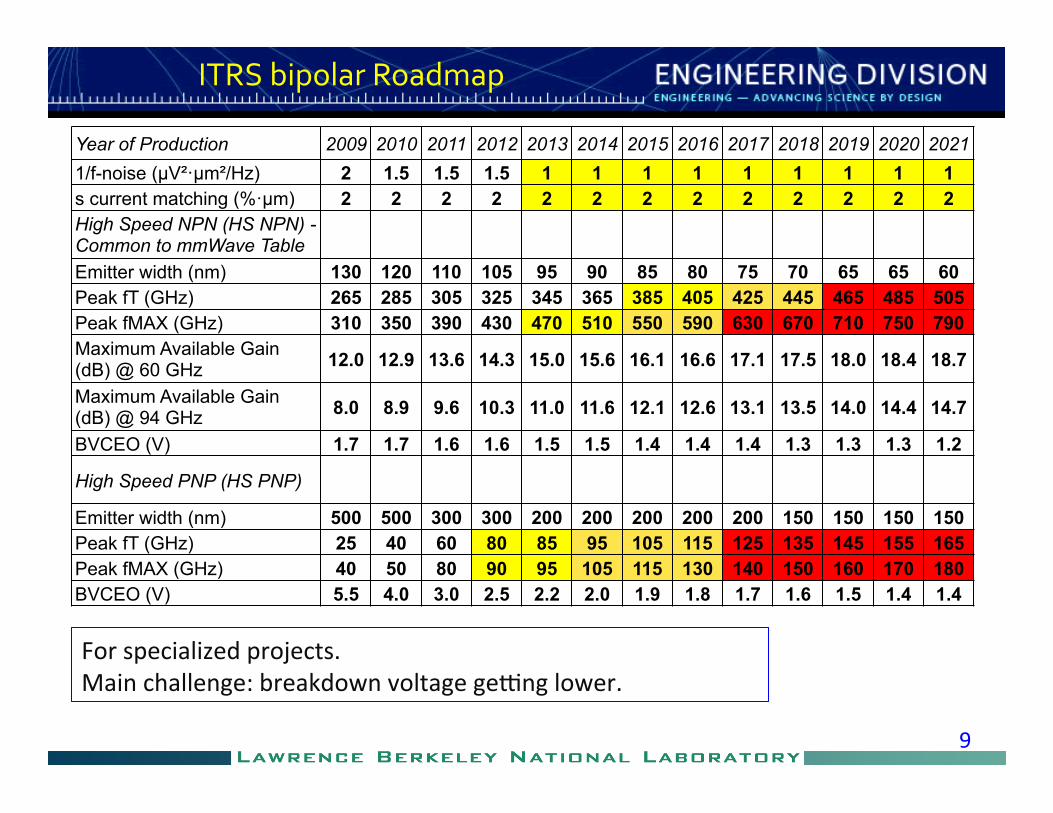
ITRS bipolar Roadmap
Year of Production 2009 2010 2011 2012 2013 2014 2015 2016 2017 2018 2019 2020 2021 1/f-noise (µV²·µm²/Hz) 2 1.5 1.5 1.5 1 1 1 1 1 1 1 1 1 s current matching (%·µm) 2 2 2 2 2 2 2 2 2 2 2 2 2 High Speed NPN (HS NPN) - Common to mmWave Table
Emitter width (nm) 130 120 110 105 95 90 85 80 75 70 65 65 60 Peak fT (GHz) 265 285 305 325 345 365 385 405 425 445 465 485 505 Peak fMAX (GHz) 310 350 390 430 470 510 550 590 630 670 710 750 790 Maximum Available Gain (dB) @ 60 GHz 12.0 12.9 13.6 14.3 15.0 15.6 16.1 16.6 17.1 17.5 18.0 18.4 18.7
Maximum Available Gain (dB) @ 94 GHz 8.0 8.9 9.6 10.3 11.0 11.6 12.1 12.6 13.1 13.5 14.0 14.4 14.7
BVCEO (V) 1.7 1.7 1.6 1.6 1.5 1.5 1.4 1.4 1.4 1.3 1.3 1.3 1.2
High Speed PNP (HS PNP)
Emitter width (nm) 500 500 300 300 200 200 200 200 200 150 150 150 150 Peak fT (GHz) 25 40 60 80 85 95 105 115 125 135 145 155 165 Peak fMAX (GHz) 40 50 80 90 95 105 115 130 140 150 160 170 180 BVCEO (V) 5.5 4.0 3.0 2.5 2.2 2.0 1.9 1.8 1.7 1.6 1.5 1.4 1.4
For specialized projects. Main challenge: breakdown voltage ge\ng lower.
9

Advanced IC processes are available thru brokers
32 nm 0.9 /1.5 7th generaGon IBM SOI technology improves energy savings for high-‐performance servers, printers, storage devices; networking, mobile, consumer, and game applicaGons. Trusted foundry access only.1
45 nm 1.0 /0.9 This energy-‐saving SOI process is suitable for a broader range of consumer electronics, including digital TVs and high-‐end mobile applicaGons. Trusted foundry access only.1
65 nm 1.0 /1.8, 2.5 Excellent for consumer electronics, wireless communicaGons, and other applicaGons requiring high performance or system-‐on-‐a-‐chip. Trusted foundry access only.1
1.2 /2.5 Tailored for power-‐sensiGve applicaGons in wireless communicaGons and consumer electronics. Trusted foundry access only.1
90 nm 1.0 /2.5 Ideal for leading-‐edge microprocessors, communicaGons, and computer data processing applicaGons. Trusted foundry access only.1
1.2 /2.5 Use for low-‐cost, high performance wireless applicaGons, as Bluetooth, WLAN, cellular handsets, mobile TV, WiMax, UWB and GPS. Trusted foundry access only.1
130 nm
1.2 /2.5 Use for low-‐cost, high performance wireless applicaGons as Bluetooth, WLAN, cellular handsets and GPS.
1.2 /2.5 Similar to 8RF-‐DM, but uses LM top metal.
40 nm
Low-‐power logic
65 nm
Standard logic, RPO Mixed-‐mode/RF, RPO, MiM
90 nm
Standard logic, RPO Mixed-‐mode/RF, RPO, MiM
0.13 µm
Standard logic, RPO Mixed-‐mode, RPO, MiM Low-‐power logic, RPO Low-‐voltage logic, RPO TSMC CMOS (mosis)
IBM CMOS (mosis)
10
VDD

Advanced IC processes available thru brokers
IBM SiGe BiCMOS Processes
Feature Size
CMOS Vdd [V]
SiGe Ft [GHz] | BVceo(1) [V]
DescripGon
HP Ft/BVceo
HB Ft/BVceo
0.13 µm 1.2, 2.5, 3.3
200 | 1.77 57 | 3.55 5th generaGon SiGe technology for advanced RADAR and mmWave applicaGons.
1.2, 2.5, 3.3
103 | 2.4 54 | 4.7 Reduced performance, cost effecGve technology for wireless applicaGons.
0.18 µm 1.8, 2.5, 3.3
120 | 2.0 20 | 4.75 4th generaGon SiGe technology best suited for wireless and high-‐speed switches.
1.8, 2.5, 3.3
60 | 3.3 29 | 6.0 Reduced performance, yet most cost effecGve SiGe technology offered.
0.25 µm 2.5, 3.3 47 | 3.3 27 | 5.7 3rd generaGon SiGe technology.
2.5, 3.3 60 | 3.2 29 | 6.0 A descendant of 7WL, it integrates 0.25 µm CMOS with the 7WL SiGe NPN.
IBM BiCMOS SiGe (MOSIS)
28 nm CMOS28LP CMOS 7LM
40 nm CMOS040 CMOS 7LM
65 nm CMOS065 CMOS 7LM
65 nm CMOS065-‐SOI SOI 6LM
St Micro CMOS (CMP)
Other less advanced and specialized processes are available thru mosis, cmp, europracIce And others! hXp://www.mosis.com hXp://cmp.imag.fr/ hXp://www.europracIce-‐ic.com/
11
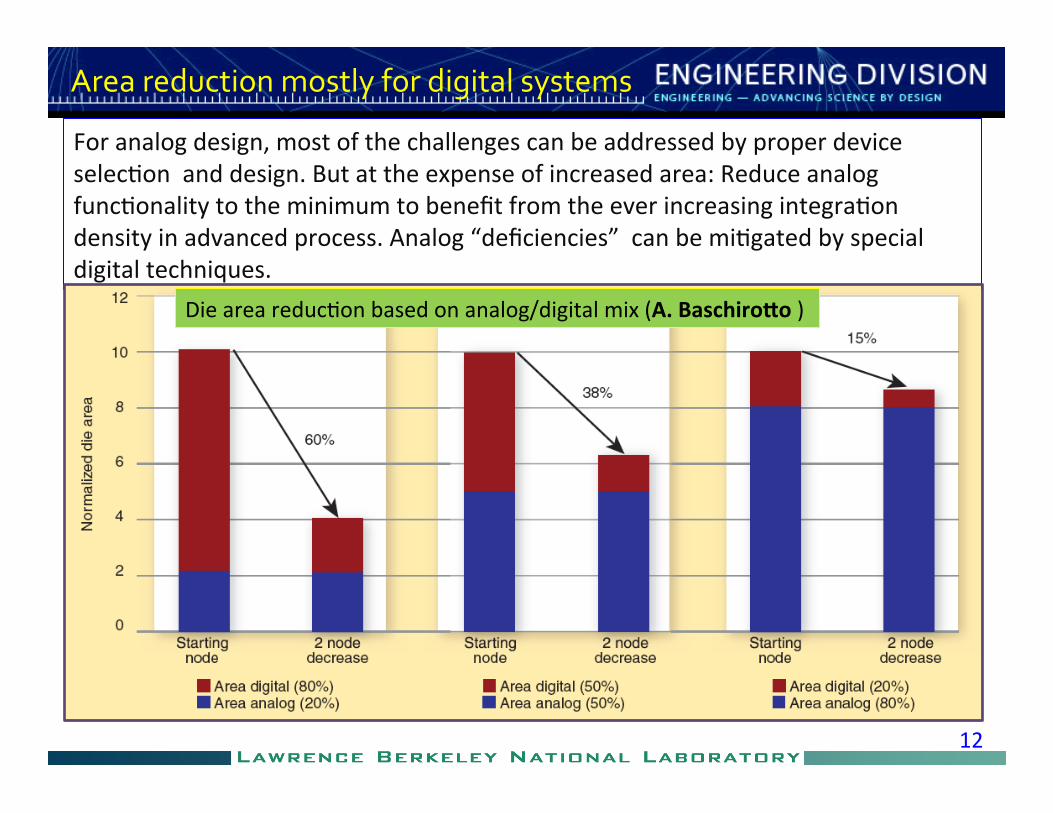
Area reduction mostly for digital systems
For analog design, most of the challenges can be addressed by proper device selecGon and design. But at the expense of increased area: Reduce analog funcGonality to the minimum to benefit from the ever increasing integraGon density in advanced process. Analog “deficiencies” can be miGgated by special digital techniques.
Die area reducGon based on analog/digital mix (A. Baschiro+o )
12

Harnessing digital processing power (a physicist perspective)
13
Ø Complex pa+ern recogniMon on chip Ø Cluster formaGon, including NN-‐style. Ø RejecGon of background clusters-‐ eg. from beam halo parGcles Ø Generic user-‐programmable DSP
Ø Pulse shape analysis. Ø Digital correcGons for anything and everything (eg. Time-‐walk).
Ø Self-‐repairing or self-‐tesMng designs. Either 100% yield or chips that automaMcally report their quality upon power-‐up (second probably easier)
Ø Self calibraMng, self Mming-‐in, etc. Ø No need to save and download threshold tunes, for example, because threshold
is automaGcally tuned on-‐chip in real Gme. Ø AutomaMng monitoring, interlocking, etc. Ø Configurable geometry. Not all pixels have to be used. User selects desired density
lower density = lower power and greater bump bonding pitch Ø Prompt hit processing (complex and fast processing of hits from pixel columns)
M. Garcia-‐Sciveres, Atlas Upgrade Week 11/16/11

Illustration of the Power of integration
>One 32bit ARM11 processor core Per 4 columns (65LP)! Fits in the dead area!
FEI4: 0.13µ ATLAS Pixel ROC ~ 20mm X 20mm Size would probably remain the same if implemented in 65 nm
14

65nm: Some transistor test result
M. Manghisoni et al. TWEPP 2011
Same gate capacitance Ø No noise degradaGon at lower nodes Ø No thermal noise increase with radiaGon Ø No or lirle 1/f noise increase with radiaGon
15

65nm: Some radiation tolerance results
Threshold voltage Leakage current
S. Bonacini et al. TWEPP 2011
65 nm devices seem to outperform their 130nm counterparts in their tolerance to ionizing radiaGon !
16

Example 1: FEI4A (ATLAS PIXELS FOR IBL)
FEI4A FEI3
Year 2010 2003
Technology 130nm 250nm
Chip size 20x19mm2 7.6x10.8mm2
AcGve area 89% 74%
Array 80x336 (26880)
18x160 (2880)
Pixel size 50x250μm2 50x400μm2
Number of transistors
87M 3.5M
Data rate 320 Mb/s 40Mb/s
Wafer yield 65% 80%
FEI4A 0.13u process Performs also most of a module Controller chip duGes
FEI3 0.25u process § Copes with higher hit rate: regional architecture and smaller pixel size
§ Improved cost effecGveness: Large chip with large acGve area § Lower power: Improved design and architecture § Increased radiaGon tolerance (~250Mrad)
17

FEI4 (cont’d)
• Column drain architecture (a la FEI3) saturates at high rate – All pixel hits are sent to periphery – Column based readout induces dead-‐Gme (during data transfer to
periphery and column readout) • ATLAS soluGons for higher rate
→ Development of regional architecture in FEI4 enabled by migraGon to a finer process
18
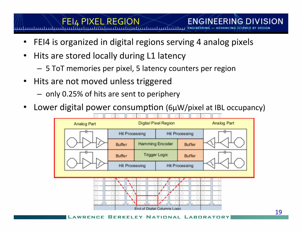
FEI4 PIXEL REGION
• FEI4 is organized in digital regions serving 4 analog pixels • Hits are stored locally during L1 latency
– 5 ToT memories per pixel, 5 latency counters per region • Hits are not moved unless triggered
– only 0.25% of hits are sent to periphery • Lower digital power consumpGon (6μW/pixel at IBL occupancy)
19

FEI4: Pixel front end
Cc
Cf2Cf1
Preamp Amp2
feedbox feedbox
Inj0
Inj1
injectIn
Cinj1
Cinj2
+local
feedback tune
FDAC4 Bit
Vfb
+local
thresholdtune
TDAC5 Bit
Vfb2
+
-
HitOutNotKill
Vth
• Similar design of analog pixel in FEI3/FEI4 • Two-‐stage amplificaGon • Clock is distributed to all digital pixel region • ToT counters within pixel digital region • ToT together with pixel address sent to periphery
FEI3 FEI4
ToT 8 bit 4 bit
TDAC 7 bit 5 bit
FDAC 3 bit 4 bit
20

FEI4A: A result
1500 2000 2500 3000 3500 4000 5000
103
102
10
1 10-‐1
Constant 849 Mean 3178 Sigma 403
2700 2900 3100 3300 3500
103
102
10
1 10-‐1
Constant 2865 Mean 3100 Sigma 26
• FEI4 bump-‐bonded to planar and 3D sensors have been successfully operated in lab test, test beams and cosmic data taking
• Tuned threshold dispersion ~30e • FEI4 low threshold operaGon (~700e) shows promising results with
reasonable dispersion • IrradiaGon tests with bare chips show no effect on threshold
dispersion and 20% increase in noise
Threshold tuning at 1400e
Threshold [e]
Threshold [e]
before tuning
aver tuning
21

Example 2: ATPIX65, next generation Atlas pixel readout prototype
• To explore the capabiliGes of advanced CMOS processes to address future HEP needs (upgrades, SLHC, )
• To have a feel of what is the best way these processes should be used to maximize ROI.
• To evaluate radiaGon hardness (mainly SEU and new damage mechanisms, if any!)
• To keep abreast of the state of the art (if one can).
22

Pixel region (2X2) a la FEI4 if implemented in 65nm
Ø Region logic synthesized from FEI4 verilog. Ø Neither 100% complete nor verified. Ø Just to have an idea on what is possible Pixel size=50X100 (?)
Ø ~FEI4 AFE equivalent
23

“FEI5” 2X2 REGION (100X200)
• SubstanGal area reducGon • UlGmately the width of a pixel will be limited by pracGcal
consideraGons (power distribuGon) and not the number of transistors!
• Room to add funcGonality
FIE4 pixel region Vs Pix65nm region (assuming y=50u)
FEI4 2X2 REGION (100X500)
If area to be kept the same as FEI4, about 4X more logic can be added
24

Snapshot of submitted pixel array
• 25 µm y cell pitch but 50µm bump y picth. • Power distribuGon will be major factor in the ulGmate minimum
dimensions • Bump mask not part of the submired layout (same size as FEI4)
25

ATPIX65A FEND BLOC DIAGRAM
Inject Bloc Preamp. 17fF Feeback cap. Variable “Rff”
Single to differenGal+ Comparator “preamp”
Comparator
TDAC (+/-‐ 4b tuning)
26
Passive RC: gate leakage limited
Ø Uses only 65nm Transistors Ø 2µA to 25µA @ 1.2V

ATPIX65A: Atlas Pixel prototype array
Pixels with Added sensors (row 11:31)
Pixels with Added mimcaps (31,27,22,18)
16 X 32 array 25µ X 125µ pixels
27

Preliminary test results
Preamp out
Single to Diff. out
Chan 15/32 Qin: 2ke
Chip found to work as expected! VDD=1.2V I= 5µA per pixel (can be as low as 2µA) 28
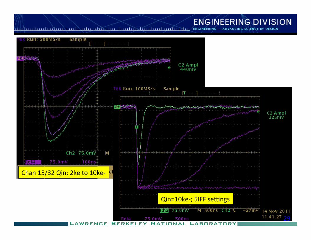
Qin=10ke-‐; 5IFF se\ngs
Chan 15/32 Qin: 2ke to 10ke-‐
29

ATPIX65A: Noise and Threshold distribution
Channels with caps or diodes
30

ATPIX65A: ENC for some columns
. . . . Channels with mimcaps
Channels with Diodes (3 types)
31

Fe55 spectrum as detected by one of the integrated sensors
32 Chip2 high gain mode. Sensor@-‐8V Very preliminary! Work in progress!
1040e-‐ pulser injecGon ~3.7keV. Assuming Cinj to be nominal.
2154 KeV (2.9KeV? May be parGal 5.9KeV charge collecGon?)
5154 KeV (theory; 5.9KeV?)
For the experiment to agree with theory (for the 5.9KeV), injecIon cap has to be corrected by 15% . SIll being reviewed!
Noise arGficially Lim
ited

Example 4: Fast, rad-‐hard CMOS direct detectors for TE
33
0.35 um CMOS TEAM2k(2009) 9.5µ pixels
4Mpix, 400 f/s
0.18 um CMOS K2 sensor (2010)
5µ pixels 16Mpix, 400 f/s
Improved radiaMon tolerance
Commercial product
0.35 um CMOS(2009) TEAM1k 1 Mpix
HIPPIX (2011) 65nm proto
FabricaMon process
Pixel pitch [µm]
Conversion Gain
[µV/e-‐]
Noise [e-‐]
Leakage current [fA]
Well depth [e-‐]
0.35 µm 9.5 9.4 30 10 90000
0.18 µm 5.0 15.5 35-‐40 4 23000
65 nm 2.5 21 50 8 18000
B.Krieger, TNS 2011

Example 4: HIPPO, a column-‐Parallel CCD readout (for X-‐ray imaging and Mu2E applications)
Ø Megapixel square sensor has ~1000 columns @ 50 μm pitch à need custom IC readout Ø No room for output amplifier à need charge-‐sensiGve readout Ø UlGmate applicaGons require intensive DSP à advanced CMOS process Ø 65nm CMOS found to be the most adequate
35 e-‐ @ 10 Mpix/s
Custom 65nm CMOS column-‐Parallel LBNL CCD
34 C. Grace, TNS 2011

HIPPO prototype chip
4 ADCs 16 SHAs 16 Analog Front ends
4200 μm
SERD
ES
(480 M
b/s)
12b (80 Msps)
HV input transistor to achieve the required noise level. Nominal transistor is too leaky! 35

HIPPO results (mixed simulation and measurements)
ResoluGon 12 b @80MHz
Noise 0.77 b
Linearity 10 b
Serial output 480 Mb/s
ADC Pitch 200 μm
ADC Area 0.35 mm2
Power per ADC 30 mW 36
Full Scale 50k / 1M e-‐
CCD charge 200ke-‐
Input noise 35 /24e-‐
Serling Gme < 15ns
Charge loss < 1%
Linearity 10 b
Power 5 mW
ADC
Preamp
J.P. Walder, TNS 2011

Conclusions
37
Unprecedented advances in IC technology are offering new ways to implement readout systems (for all kind of detector systems). New challenges seem to be more addressable with scaled down technologies. Future systems will require smaller geometries, lower power, higher level of processing, high radiaMon tolerance, lower cost per funcMon, …etc Among the advantages of newer technologies are:
Very high integraGon density Inherent high radiaGon tolerance A reasonable number of device types for extra design flexibility Availability of high quality passives A high number of metal levels
Skewing the mix of funcMonal blocks towards digital would result in a be+er area usage and chip yield. Not to menMon flexibility (programmability) and ProducMvity (think advanced digital tools) A myriad of challenges related to ultra complex processes and ultra small devices are associated with these technologies. For some of these, miGgaGon techniques are readily available A unique challenge to the research community is perhaps the cost of these advanced processes (given the low volume usually involved). Common wisdom applies: for some applicaMons plain old technologies would remain the opMmal choice.

Acknowledgements
38
Thank You Many Thanks to all people whose work has been menGoned and to my colleagues at LBNL For their help. Please refer to the referenced work for more exciGng details.