cpc1788 single-pole, normally open integrated c d isoplus
TRANSCRIPT
INTEGRATED CIRCUITS DIVISION
DS-CPC1788-R04 www.ixysic.com 1
e3
Characteristics
Features• 2.45ADC Load Current with 5°C/W Heat Sink• Low 1.25 On-Resistance• 1000VP Blocking Voltage• 2500Vrms Input/Output Isolation• Low Thermal Resistance (0.3 °C/W)• Electrically Non-conductive Thermal Pad for Heat
Sink Applications• Low Drive Power Requirements• Arc-Free With No Snubbing Circuits• No EMI/RFI Generation• Machine Insertable, Wave Solderable
Applications• Industrial Controls / Motor Control• Robotics• Medical Equipment—Patient/Equipment Isolation• Instrumentation• Multiplexers• Data Acquisition• Electronic Switching• I/O Subsystems• Meters (Watt-Hour, Water, Gas)• Transportation Equipment• Aerospace/Defense
Approvals• UL 508 Certified Component: File E69938
Pin Configuration
DescriptionIXYS Integrated Circuits Division and IXYS have combined to bring OptoMOS® technology, reliability and compact size to a new family of high-power Solid State Relays.
As part of this new family, the CPC1788 single-pole normally open (1-Form-A) DC Solid State Power Relay employs optically coupled MOSFET technology to provide 2500Vrms of input to output isolation.
The optically coupled outputs, that use patented OptoMOS architecture, are controlled by a highly efficient GaAIAs infrared LED. The combination of low on-resistance and high load current handling capability makes this relay suitable for a variety of high performance DC switching applications.
The unique ISOPLUS-264 package pioneered by IXYS enables Solid State Relays to achieve the highest load current and power ratings. This package features a unique IXYS process where the silicon chips are soft soldered onto the Direct Copper Bond (DCB) substrate instead of the traditional copper leadframe. The DCB ceramic, the same substrate used in high power modules, not only provides 2500Vrms isolation, but also very low thermal resistance (0.3 °C/W).
Ordering Information
Switching Characteristics
Parameter Rating Units
Blocking Voltage 1000 VP
Load Current, TA=25°C:
With 5°C/W Heat Sink 2.45ADC
No Heat Sink 1
On-Resistance (max) 1.25
RJC 0.3 °C/W
1 2 3 4
+ - - +
Part Description
CPC1788J ISOPLUS-264 Package (25 per tube)
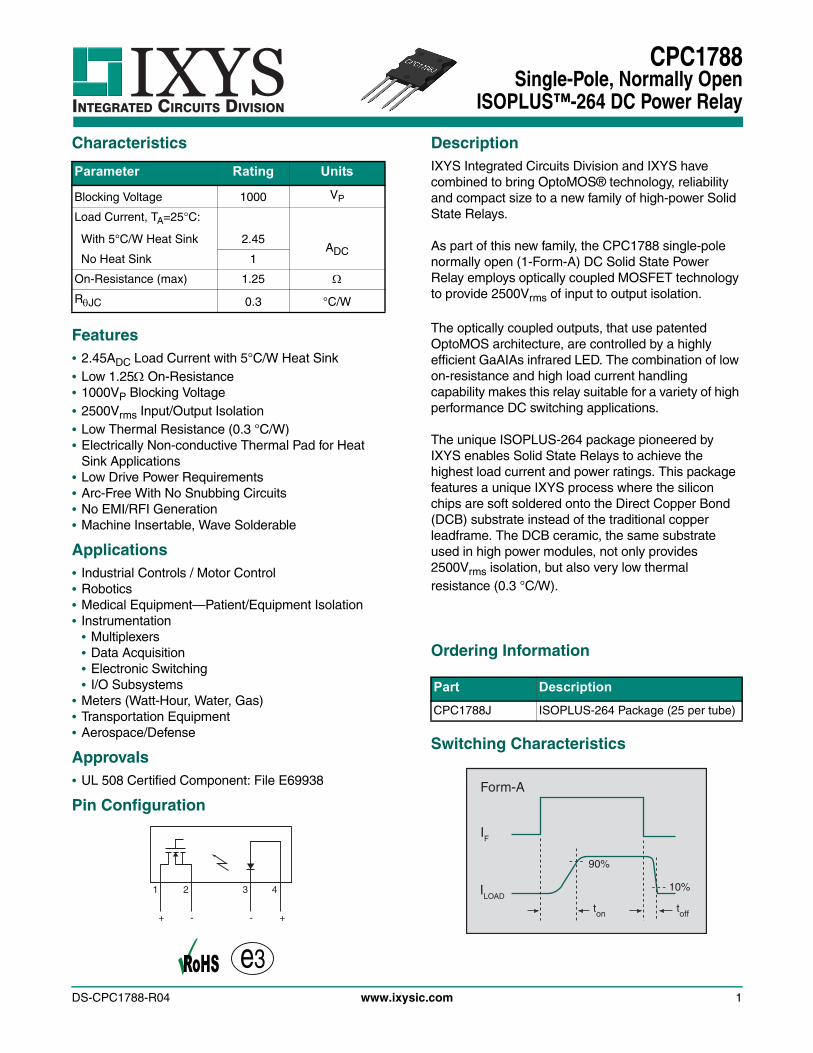
Form-A
IF
ILOAD10%
90%
ton toff
CPC1788Single-Pole, Normally Open
ISOPLUS™-264 DC Power Relay

INTEGRATED CIRCUITS DIVISION
R04 www.ixysic.com 2
CPC1788
1 Specifications
1.1 Absolute Maximum Ratings @ 25°C
Absolute maximum ratings are stress ratings. Stresses in excess of these ratings can cause permanent damage to the device. Functional operation of the device at conditions beyond those indicated in the operational sections of this data sheet is not implied.
1.2 Electrical Characteristics @ 25°C
1 Higher load currents possible with proper heat sinking.2 Measurement taken within 1 second of on-time.3 For applications requiring high temperature operation (TC > 60ºC) a LED drive current of 20mA is recommended.
Symbol Ratings Units
Blocking Voltage 1000 VP
Reverse Input Voltage 5 V
Input Control Current 100 mA
Peak (10ms) 1 ADC
Input Power Dissipation 150 mW
Isolation Voltage, Input to Output 2500 Vrms
Operational Temperature -40 to +85 °C
Storage Temperature -40 to +125 °C
Parameter Conditions Symbol Minimum Typical Maximum Units
Output Characteristics
Load Current 1
Peak t10ms
IL- -
12 AP
Continuous No Heat Sink 1
Continuous TC=25°C 10.3 ADC
Continuous TC=99°C IL(99) 1.2
On-Resistance 2 IF=10mA, IL=1A RON - 1 1.25
Off-State Leakage Current VL=1000VP ILEAK - - 1 A
Switching Speeds
Turn-OnIF=20mA, VL=10V
ton - 2.85 20ms
Turn-Off toff - 0.11 5
Output Capacitance VL=25V, f=1MHz Cout - 640 - pFInput Characteristics
Input Control Current to Activate 3 IL=1A IF - - 10 mA
Input Control Current to Deactivate - IF 0.6 - - mA
Input Voltage Drop IF=5mA VF 0.9 1.2 1.4 V
Reverse Input Current VR=5V IR - - 10 AInput/Output Characteristics
Capacitance, Input-to-Output - CI/O - 1 - pF
INTEGRATED CIRCUITS DIVISION
3 www.ixysic.com R04
CPC1788
2 Thermal Characteristics
2.1 Thermal Management
Device high current characterization was performed using Kunze heat sink KU 1-159, phase change thermal interface material KU-ALC 5, and transistor clip KU 4-499/1. This combination provided an approximate junction-to-ambient thermal resistance of 12.5°C/W.
2.2 Heat Sink Calculation
Higher load currents are possible by using lower thermal resistance heat sink combinations.
Parameter Conditions Symbol Minimum Typical Maximum Units
Thermal Resistance (Junction to Case) - RJC - - 0.3 °C/W
Thermal Resistance (Junction to Ambient) Free Air RJA - 33 - °C/W
Junction Temperature (Operating) - TJ -40 - 100 °C
TJ = Junction Temperature (°C), TJ ≤ 100°C *TA = Ambient Temperature (°C)IL(99) = Load Current with Case Temperature @ 99°C (ADC)IL = Desired Operating Load Current (ADC), IL ≤ IL(MAX)
RθJC = Thermal Resistance, Junction to Case (°C/W) = 0.3°C/WRθCA = Thermal Resistance of Heat Sink & Thermal Interface Material , Case to Ambient (°C/W)PD(99) = Maximum power dissipation with case temperature held at 99ºC = 3.33W
* Elevated junction temperature reduces semiconductor lifetime.
Heat Sink Rating
RθCA = - RθJC
(TJ - TA) IL(99)2
IL2 • PD(99)

INTEGRATED CIRCUITS DIVISION
R04 www.ixysic.com 4
CPC1788
3 Performance Data
Unless otherwise specified, all performance data was acquired without the use of a heat sink.
The Performance data shown in the graphs above is typical of device performance. For guaranteed parameters not indicated in the written specifications, please contact our application department.
35
30
25
20
15
10
5
01.30 1.31 1.32 1.33 1.34
Dev
ice
Co
un
t (N
)
Typical LED Forward Voltage Drop(N=50, IF=10mA, TA=25ºC)
LED Forward Voltage (V)
35
30
25
20
15
10
5
02.15 2.50 2.85 3.553.20 3.90
Dev
ice
Co
un
t (N
)
Typical Turn-On Time(N=50, IF=20mA, IL=1ADC, TA=25ºC)
Turn-On (ms)
0.080 0.110 0.1400.065 0.095 0.125
Dev
ice
Co
un
t (N
)
25
20
15
10
5
0
CPC1788Typical Turn-Off Time
(N=50, IF=20mA, IL=1ADC, TA=25ºC)
Turn-Off (ms)
35
30
25
20
15
10
5
00.900 0.925 0.950 0.975 1.000 1.025
Dev
ice
Co
un
t (N
)
Typical On-Resistance Distribution(N=50, IF=10mA, IL=1ADC, TA=25ºC)
On-Resistance (Ω)
Typical LED Forward Voltage Dropvs. Temperature
LE
D F
orw
ard
Vo
ltag
e D
rop
(V
) 1.8
1.6
1.4
1.2
1.0
0.8-40 -20 0 20 40 60 80 120100
Temperature (ºC)
IF=50mA
IF=10mAIF=20mA
LED Forward Current (mA)0 5 10 15 20 25 30 35 40 45 50
1211109876543210
Typical Turn-Onvs. LED Forward Current
(IL=250mADC)
Turn
-On
(m
s)
LED Forward Current (mA)0 5 10 15 20 25 30 35 40 45
0.145
0.140
0.135
0.130
0.125
0.120
0.115
0.110
0.105
0.10050
Typical Turn-Offvs. LED Forward Current
(IL=250mADC)
Turn
-On
(m
s)
LE
D C
urr
ent
(mA
)
-40
5.04.54.03.53.02.52.01.51.00.5
0-20 0 20 40 60 80 100
Typical IF for Switch Operationvs. Temperature
(IL=250mADC)
Temperature (ºC)-40
7
6
5
4
3
2
1
0-20 0 20 40 60 80 100
Typical Turn-On vs. Temperature(IL=250mADC)
Temperature (ºC)
IF=10mA
IF=20mA
Turn
-On
(m
s)
-40
0.24
0.21
0.18
0.15
0.12
0.09
0.06
0.06-20 0 20 40 60 80 100
Typical Turn-Off vs. Temperature(IL=250mADC)
Temperature (ºC)
IF=20mA
IF=10mA
Turn
-Off
(m
s)

INTEGRATED CIRCUITS DIVISION
5 www.ixysic.com R04
CPC1788
Unless otherwise specified, all performance data was acquired without the use of a heat sink.
The Performance data shown in the graphs above is typical of device performance. For guaranteed parameters not indicated in the written specifications, please contact our application department.
-40
1.8
1.6
1.4
1.2
1.0
0.8
0.6
0.4
0.2
0-20 0 20 40 60 80 100
Typical On-Resistancevs. Temperature
(IF=10mA, IL=250mADC)
Temperature (ºC)
On
-Res
ista
nce
(Ω
)
-40
2.22.01.81.61.41.21.00.80.60.40.20
-20 0 20 40 60 80 100
Typical On-Resistancevs. Temperature
(IF=10mA, IL=Max Rated)
Temperature (ºC)
On
-Res
ista
nce
(Ω
)
Lo
ad C
urr
ent
(A)
0
0.500.450.400.350.300.250.200.150.100.05
00.1 0.2 0.4 0.50.3 0.6
Typical Load Currentvs. Load Voltage
(IF=10mA, TA=25ºC)
Load Voltage (V)
Temperature (ºC)0 20 40 60 80 100
Lo
ad C
urr
ent
(AD
C)
0
1
2
3
4
5
6
Maximum Load Currentvs. Temperature(With Heat Sink)
1ºC/W
Free Air
10ºC/W
5ºC/W
-40
1160
1140
1120
1100
1080
1060
1040
1020
1000-20 0 20 40 60 80 100
Blocking Voltage vs. Temperature
Temperature (ºC)
Blo
ckin
g V
olt
age
(VP)
-40
0.7
0.6
0.5
0.4
0.3
0.2
0.1
0-20 0 20 40 60 80 100
Typical Leakage vs. TemperatureMeasured Across Pins 1&2
(VL=1000VP)
Lea
kag
e (μ
A)
Temperature (ºC)
Lo
ad C
urr
ent
(A)
Energy Rating CurveFree Air, No Heat Sink
15.013.512.010.59.07.56.04.53.01.50
10µs 100µs 1ms 10ms 100ms 1s 10s 100s
Time
INTEGRATED CIRCUITS DIVISION
R04 www.ixysic.com 6
CPC1788
4 Manufacturing Information
4.1 Moisture Sensitivity
All plastic encapsulated semiconductor packages are susceptible to moisture ingression. IXYS Integrated Circuits Division classified all of its plastic encapsulated devices for moisture sensitivity according to the latest version of the joint industry standard, IPC/JEDEC J-STD-020, in force at the time of product evaluation. We test all of our products to the maximum conditions set forth in the standard, and guarantee
proper operation of our devices when handled according to the limitations and information in that standard as well as to any limitations set forth in the information or standards referenced below.
Failure to adhere to the warnings or limitations as established by the listed specifications could result in reduced product performance, reduction of operable life, and/or reduction of overall reliability.
This product carries a Moisture Sensitivity Level (MSL) rating as shown below, and should be handled according to the requirements of the latest version of the joint industry standard IPC/JEDEC J-STD-033.
4.2 ESD Sensitivity
This product is ESD Sensitive, and should be handled according to the industry standard JESD-625.
4.3 Reflow Profile
This product has a maximum body temperature and time rating as shown below. All other guidelines of J-STD-020 must be observed.
4.4 Board Wash
IXYS Integrated Circuits Division recommends the use of no-clean flux formulations. However, board washing to remove flux residue is acceptable. Since IXYS Integrated Circuits Division employs the use of silicone coating as an optical waveguide in many of its optically isolated products, the use of a short drying bake may be necessary if a wash is used after solder reflow processes. Chlorine-based or Fluorine-based solvents or fluxes should not be used. Cleaning methods that employ ultrasonic energy should not be used.
Device Moisture Sensitivity Level (MSL) Rating
CPC1788J MSL 1
Device Maximum Temperature x Time
CPC1788J 245°C for 30 seconds
e3

INTEGRATED CIRCUITS DIVISION
7 www.ixysic.com R04
CPC1788
4.5 Mechanical Dimensions
NOTE: Back-side heat sink meets 2500Vrms isolation to the pins.
26.162 ± 0.254(1.030 ± 0.010)
19.914 ± 0.254(0.784 ± 0.010)
20.396 ± 0.508(0.803 ± 0.020)
15.240 ± 0.508(0.600 ± 0.020)
3.810 ± 0.254(0.150 ± 0.010)
2.362 ± 0.381(0.093 ± 0.015)
0.635 ± 0.076(0.025 ± 0.003) 2.794 ± 0.127
(0.110 ± 0.005)
5.029 ± 0.127(0.198 ± 0.005) 1.181 ± 0.076
(0.047 ± 0.003)
1.930 ± 0.381(0.076 ± 0.015)
17.221 ± 0.254(0.678 ± 0.010)
20.600 ± 0.254(0.811 ± 0.010)
1.270 TYP(0.050 TYP)
DIMENSIONSmm
(inches)
For additional information please visit our website at: www.ixysic.comIXYS Integrated Circuits Division makes no representations or warranties with respect to the accuracy or completeness of the contents of this publication and reserves the right to make changes to specifications and product descriptions at any time without notice. Neither circuit patent licenses nor indemnity are expressed or implied. Except as set forth in IXYS Integrated Circuits Division’s Standard Terms and Conditions of Sale, IXYS Integrated Circuits Division assumes no liability whatsoever, and disclaims any express or implied warranty, relating to its products including, but not limited to, the implied warranty of merchantability, fitness for a particular purpose, or infringement of any intellectual property right.
The products described in this document are not designed, intended, authorized or warranted for use as components in systems intended for surgical implant into the body, or in other applications intended to support or sustain life, or where malfunction of IXYS Integrated Circuits Division’s product may result in direct physical harm, injury, or death to a person or severe property or environmental damage. IXYS Integrated Circuits Division reserves the right to discontinue or make changes to its products at any time without notice.
Specification: DS-CPC1788-R04©Copyright 2012, IXYS Integrated Circuits DivisionAll rights reserved. Printed in USA.12/17/2012
Mouser Electronics
Authorized Distributor
Click to View Pricing, Inventory, Delivery & Lifecycle Information: IXYS:
CPC1788J