cpu12 design using vhdl - university of victoria unit state diagram ..... 27 4.2.3. the control...
TRANSCRIPT

CPU12 Design Using VHDL
The CPU of Motorola HC12 Microcontroller Research Project Report 2009
Ibrahim Hejab Hazmi Master of Electronic Engineering - Coursework
With the guidance of:
Dr. Paul Beckett School of Electronic and Computer Engineering, RMIT University

CPU12 Design Ibrahim Hazmi -2009
Page 2
Acknowledgement
First of all, Thank God, the one who gave me this chance to learn and meet experts in the field of Digital
System Design. And I am greatly thankful to Dr. Paul Beckett for his patience support and guidance in
my project.
I am also grateful to my friends, Ahmed and Saleh for their co-operation in providing a health
environment for discussions about how to get things done especially, report writing.
I would not forget my small family, my wife, Maryam, and the three roses, Tranim, Layan and Marya. I
always get the real support from them.
Ibrahim Hazmi
CPU12 Design Ibrahim Hazmi -2009
Page 3
Abstract
When designing a microcontroller, it is important to think the way that microcontrollers work. Simply,
it is data transfer and manipulation with sequential control for the data flow. CPU of the
microcontroller is responsible for doing all these operations in addition to managing the
communications with all other parts including memories and I/O ports.
My project objective is to design the CPU12, CPU of the HC12 microcontroller. Apart from memory, it
consists simply from Data Path Unit and Control Unit. The idea is to design these tow units of the
CPU12 individually then combine them together to run a simple sequence of instructions. There was a
challenge to make the design as structural as it could be and that has been satisfied for the Data Path
Unit whereas Control unit was designed as a state machine which is totally in behavioral Level.
The main Components of the Data Path are the Register Block and the ALU; these are responsible for
instruction execution and they contribute in the effective address calculations. The Address Calculation
Unit is also is included in the Data Path and responsible for effective address calculation for Indexed
and relative Addressing Modes. Parallel 16-bit Multiplier and Fast 32-bit Divider have been added to
the ALU offering fast mathematical operations and reducing the number of cycles that needed for
Multiplication and Division instructions.
The Design of the Control Unit in this project is simply a state diagram starts with the fetch, decode and
execute states considering the addressing modes in which execution phase might split into many states
depends on the addressing mode of the current instruction. The state diagram of the Control Unit
contains “Twelve” states including start state.
The two Units have been connected together to run a simple instruction (ADDA) for all addressing
modes and give results showing all States, Units and signals that are involved to execute such
instruction. And finally, the result of the addition is stored in the accumulator A in all cases.
CPU12 Design Ibrahim Hazmi -2009
Page 4
Table of Contents Acknowledgement ........................................................................................................................................ 2 Abstract ......................................................................................................................................................... 3 1. Introduction .......................................................................................................................................... 6
1.1. Background .................................................................................................................................. 6 1.2. Project Objectives ........................................................................................................................ 7 1.3. Project Significance ...................................................................................................................... 7 1.4. Project Description ...................................................................................................................... 8 1.4.1. The Project Specific Work ............................................................................................................ 8 1.4.2. Project Outcomes: ....................................................................................................................... 9
2. Literature Review ............................................................................................................................... 10 2.1. Design Representation: .............................................................................................................. 10 2.2. Examples of Microcontrollers/Processors that I’ve started with .............................................. 12 2.2.1. The EC-1 and EC-2 General-Purpose Microprocessors .............................................................. 12 2.2.2. From LC-3 to HC12: ................................................................................................................... 13 2.2.3. HC11 ........................................................................................................................................... 14
3. Methodology ...................................................................................................................................... 15 3.1. Introduction ............................................................................................................................... 15 3.2. Overview of the Design .............................................................................................................. 16 3.2.1. The Main Block Diagram ............................................................................................................ 16 3.2.2. The Three Sub-Main Units ......................................................................................................... 17 3.2.2.1. The Data Path including the Address Calculation Unit .............................................................. 17 3.2.2.2. The Control Unit ......................................................................................................................... 18 3.2.2.3. The Memory Access Unit ........................................................................................................... 18
4. Detailed Description of the design ..................................................................................................... 19 4.1. Data Path Components .............................................................................................................. 19 4.1.1. Register Block ............................................................................................................................. 20 4.1.1.1. Accumulators ............................................................................................................................. 22 4.1.2. ALU Block ................................................................................................................................... 23 4.1.2.1. Basic Arithmetic, Logic and Shift (ALSU) Cell ............................................................................. 23 4.1.2.2. Address Calculation Unit ............................................................................................................ 25 4.2. Control Unit................................................................................................................................ 26 4.2.1. The Job of Control Unit .............................................................................................................. 26 4.2.2. Control Unit State Diagram ........................................................................................................ 27 4.2.3. The Control Words for Data Path Operations: .......................................................................... 28 4.3. Results (Timing Simulation) ....................................................................................................... 30 4.4. Project Outcomes: Evaluation (My Suggestions) ...................................................................... 36
Conclusions ................................................................................................................................................. 37 References................................................................................................................................................... 38 Appendices .................................................................................................................................................. 39
CPU12 Design Ibrahim Hazmi -2009
Page 5
Table of Figures
Figure 1: HC12 ............................................................................................................................................... 8
Figure 2: Gajski and Kuhn’s Y Chart (1982) ................................................................................................. 10
Figure 3: Level of Abstraction ..................................................................................................................... 11
Figure 4: Table of EC-2 Instruction Set with its Block Diagram ................................................................... 12
Figure 5: LC3 Instruction Set and its Block Diagram; (Similar to my Block Diagram).................................. 13
Figure 6: HC11Block Diagram ...................................................................................................................... 14
Figure 7: The Main Block Diagram of CPU12 showing the suggested 4 sub-main blocks of the design .... 16
Figure 8: The Data Path Unit Including the Address Calculation Circuit ..................................................... 17
Figure 9: The Control Unit Overview........................................................................................................... 18
Figure 10: Suggested Image of the Memory Access Unit and PFU ............................................................. 18
Figure 11: Suggested Block Diagram of the Register Block connected to the ALU in the Data Path Unit .. 19
Figure 12: CPU12 Registers ......................................................................................................................... 20
Figure 13: CPU12 Suggested Registers Block Diagram ............................................................................... 21
Figure 14: Accumulators A, B and D ............................................................................................................ 22
Figure 15: ALU Including Advanced Math (Multiplier and Divider) ............................................................ 23
Figure 16: Basic Cell of Arithmetic, Logic and Shift Operations .................................................................. 24
Figure 17: Instruction Format with Part of Decoding Unit ......................................................................... 26
Figure 18: The State diagram of the Control Unit ....................................................................................... 27
Table 1: Accumulators Logic ....................................................................................................................... 22
Table 2: ALSU Truth table............................................................................................................................ 24
Table 3: Some Control Signals for ATT ALL STATES ..................................................................................... 28
Table 4: Some Control Signals for different Addressing Modes ................................................................. 29
Table 5: My Simulation Inputs and Some Expected Results ....................................................................... 29
CPU12 Design Ibrahim Hazmi -2009
Page 6
1. Introduction
1.1. Background
The combination of designing Embedded Systems and Using High Level Synthesis Tools is one of the
interesting areas in Electronic design. It gives the ability to make soft cores for all
microcontrollers/Microprocessors in which embedded system designers will have additional tools
between their hands to accelerate their innovations.
Programmable logic has progressed from being used as glue logic to today’s FPGAs, where complete
system designs can be implemented on a single device. With the availability of multimillion-gate FPGA
architectures, and support for various third-party EDA tools, a designer can use a design flow similar to
that of traditional standard cell ASIC devices to create system-on-a-programmable-chip (SOPC) designs
in FPGAs [3], or System-on-chip design (SoC). SoC design methodologies show up as a natural and
productive method to implement embedded systems. There are several processor cores that are
commonly used in SoC applications, both commercial cores and free or open cores [4], such as HC11.
It is worth it to pick-up a microcontroller which has mostly all the features of performing digital process
and control from the embedded system basket. That was Motorola HC12 and this project is to make a
soft-core for CPU12, the Central Processing Unit of HC12. It seams easy, as the soft-core of HC11 has
already been designed, but this is for a designer who has done at least one microcontroller design
before. Yet the level of abstraction of My HC12 is different from the one in which HC11 was
implemented. Overall, it was excellent experience doing such design; tough, hard, but very interesting.
As a start point in designing a microcontroller/Microprocessor, the design can be divided into two main
parts, the Data Path and the Control Unit. The Data Path is responsible for all the operations on the
data. It includes (1) ALU, (2) registers and other memory elements for the temporary storage of data,
and (3) buses and multiplexers for the transfer of data between the different components in the Data
Path. The Control Unit is responsible for controlling all the operations of the Data Path by providing
appropriate control signals to the Data Path at the appropriate time [1].

CPU12 Design Ibrahim Hazmi -2009
Page 7
1.2. Project Objectives
As mentioned before, this project is conducted to re-design CPU12 by using VHDL. Project objectives
can be narrowed down to the following:
• Re-designing CPU12 as an excellent example of embedded system design
o Suggesting a sensible diagram of the whole system
o Partitioning the main block into smaller designable blocks
o Connecting the different blocks together in the sense of sequential operation.
• Designing CPU12 as a soft-core by using VHDL
o Offering a soft-core for HC12 in VHDL text form.
o Practicing new EDA Tools for FPGA and CPLD design.
1.3. Project Significance
From such project work, new Embedded System designers can gain the following:
1. Practical and Detailed Understanding of Embedded System Design.
2. Combining the Understanding of the Embedded System with the skills in HDL Design.
3. HC12 is a microcontroller which has everything inside, so it is worth it to start with.
4. According to my knowledge, HC12 is not available to the public as a VHDL code, so it is great if
we could make it available for academic and research purposes.

CPU12 Design Ibrahim Hazmi -2009
Page 8
1.4. Project Description
CPU12 is the heart of HC12. Fig1.1 shows HC12 components including CPU12. It seams like a black box
and that what the project aims to, take-off the black mask by clarifying its function(s) and
understanding the process of controlling its operations. Then, VHDL is the media of putting these
outcomes together in order to design the CPU12.
Figure 1: HC12
1.4.1. The Project Specific Work
The Project is to design the tow units of the CPU12, (Data Path and Control Unit), individually then
combine them together to run a simple sequence of instructions. Additional challenge is to make the
design as structural as it possible and behavioral Level where it needs to be.

CPU12 Design Ibrahim Hazmi -2009
Page 9
1.4.2. Project Outcomes:
• Design Cpu12 and make it works properly for the selected samples of its instruction set and
this will be met by designing the following:
o Data Path Unit which consist of
§ Register Block accommodating all CPU12 internal registers
• Accumulators A, B and D(A:B)
• Index registers X and Y
• Stack Pointer (SP) and Program Counter (PC)
• Condition Code Register (CC) – ALU sensor and Control Unit input
§ ALU, Arithmetic, Logic and Shift unit which does all data manipulations where
data could come from registers or memory. This includes
• Designing a basic cell for all simple ALU operations, and
• Extra Circuits to gain more operations and obtain the right condition
Code results for all operations
• Advanced Mathematical Circuits for Multiplication and Division
§ Address Calculation Circuit connected to Register Block and ALU to provide
accurate effective address for all addressing modes.
o Control Unit which is, again, a simple state diagram shows all possible states that
include all addressing modes.
• Combining the Two Parts together.
• Simulation (Test Bench and Timing Diagrams)
CPU12 Design Ibrahim Hazmi -2009
Page 10
2. Literature Review
In this chapter, I am going to talk about two issues. The first issue is about the Design representation
using HDL Design environment and High Level Synthesis tools. And the second one is about some
examples that I’ve used as guidance during my design processes.
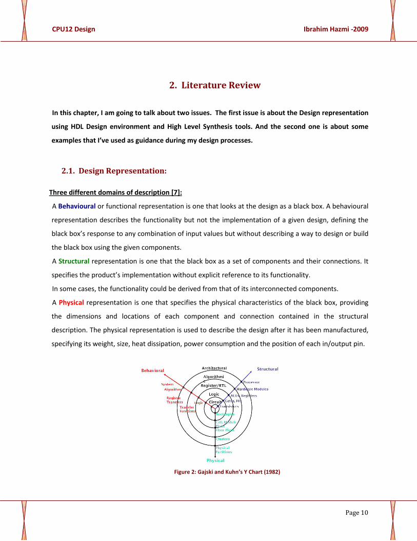
2.1. Design Representation:
Three different domains of description [7]:
A Behavioural or functional representation is one that looks at the design as a black box. A behavioural
representation describes the functionality but not the implementation of a given design, defining the
black box’s response to any combination of input values but without describing a way to design or build
the black box using the given components.
A Structural representation is one that the black box as a set of components and their connections. It
specifies the product’s implementation without explicit reference to its functionality.
In some cases, the functionality could be derived from that of its interconnected components.
A Physical representation is one that specifies the physical characteristics of the black box, providing
the dimensions and locations of each component and connection contained in the structural
description. The physical representation is used to describe the design after it has been manufactured,
specifying its weight, size, heat dissipation, power consumption and the position of each in/output pin.
Figure 2: Gajski and Kuhn’s Y Chart (1982)
CPU12 Design Ibrahim Hazmi -2009
Page 11
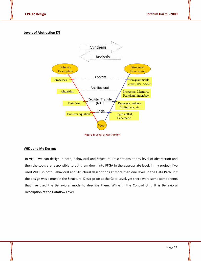
Levels of Abstraction [7]
Figure 3: Level of Abstraction
VHDL and My Design:
In VHDL we can design in both, Behavioral and Structural Descriptions at any level of abstraction and
then the tools are responsible to put them down into FPGA in the appropriate level. In my project, I’ve
used VHDL in both Behavioral and Structural descriptions at more than one level. In the Data Path unit
the design was almost in the Structural Description at the Gate Level, yet there were some components
that I’ve used the Behavioral mode to describe them. While In the Control Unit, It is Behavioral
Description at the Dataflow Level.
CPU12 Design Ibrahim Hazmi -2009
Page 12
2.2. Examples of Microcontrollers/Processors that I’ve started with
I have seen many examples of microcontrollers/microprocessors before and during my work on CPU12,
but I found the following three examples were much helpful to get a clear imagination of my design.
The first example was the two versions of simple EC Microprocessors in which I’ve started to
understand how microprocessor works. The second one, LC3, was my guide to imagine the block
diagram which met my design requirements. And HC11 is a great example that should be presented in
this regard as it is the previous generation of HC12 in the HC family.
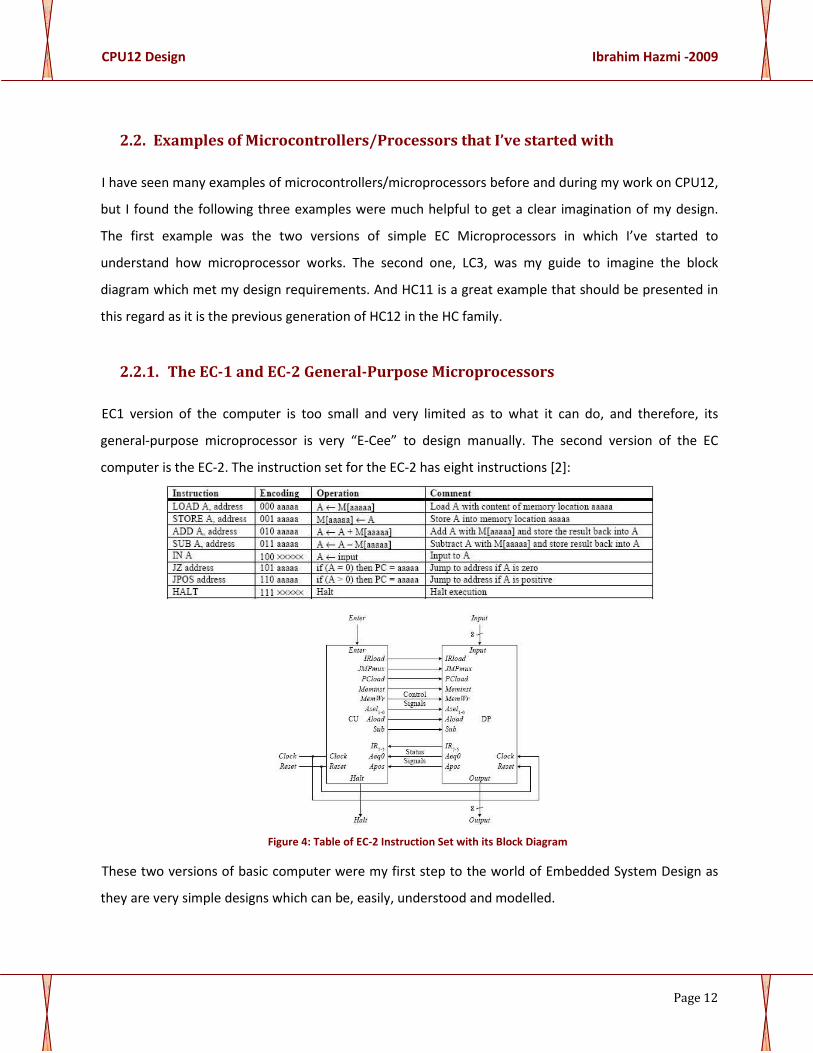
2.2.1. The EC-1 and EC-2 General-Purpose Microprocessors
EC1 version of the computer is too small and very limited as to what it can do, and therefore, its
general-purpose microprocessor is very “E-Cee” to design manually. The second version of the EC
computer is the EC-2. The instruction set for the EC-2 has eight instructions [2]:
Figure 4: Table of EC-2 Instruction Set with its Block Diagram
These two versions of basic computer were my first step to the world of Embedded System Design as
they are very simple designs which can be, easily, understood and modelled.
CPU12 Design Ibrahim Hazmi -2009
Page 13
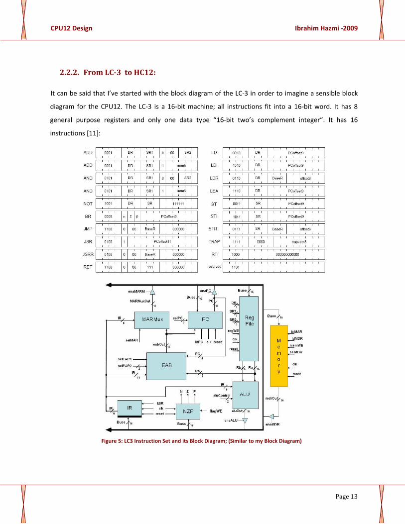
2.2.2. From LC-3 to HC12:
It can be said that I’ve started with the block diagram of the LC-3 in order to imagine a sensible block
diagram for the CPU12. The LC-3 is a 16-bit machine; all instructions fit into a 16-bit word. It has 8
general purpose registers and only one data type “16-bit two’s complement integer”. It has 16
instructions [11]:
Figure 5: LC3 Instruction Set and its Block Diagram; (Similar to my Block Diagram)
CPU12 Design Ibrahim Hazmi -2009
Page 14
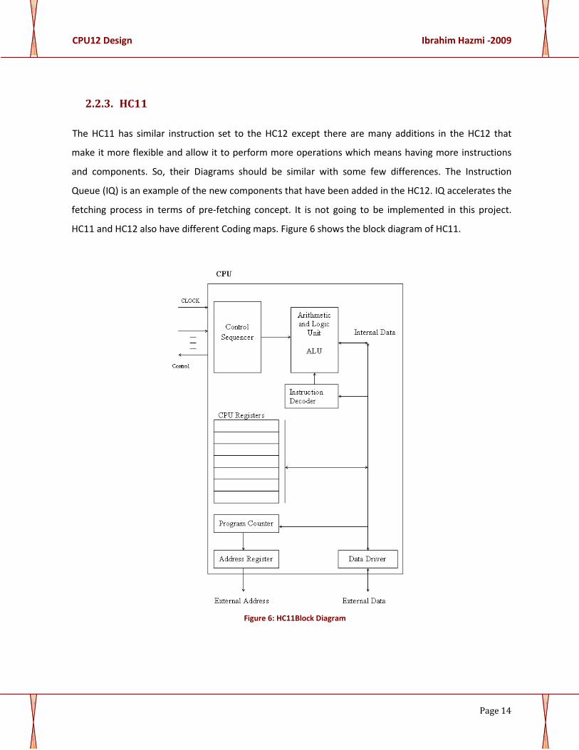
2.2.3. HC11
The HC11 has similar instruction set to the HC12 except there are many additions in the HC12 that
make it more flexible and allow it to perform more operations which means having more instructions
and components. So, their Diagrams should be similar with some few differences. The Instruction
Queue (IQ) is an example of the new components that have been added in the HC12. IQ accelerates the
fetching process in terms of pre-fetching concept. It is not going to be implemented in this project.
HC11 and HC12 also have different Coding maps. Figure 6 shows the block diagram of HC11.
Figure 6: HC11Block Diagram

CPU12 Design Ibrahim Hazmi -2009
Page 15
3. Methodology
3.1. Introduction
It was not possible to design a microcontroller with misunderstanding of how microcontroller works.
So, it was the beginning to get this understanding achieved by doing some research and picking-up
some examples to Imitate. While doing such work I found a beautiful quote that might shorten the
way for new designers in embedded system:
“In designing a CPU, we must first define its instruction set, and how the instructions are
encoded and executed. We need to answer questions such as how many instructions do
we want? What are the instructions? What operation code (opcode) do we assign to
each of the instructions? How many bits do we use to encode an instruction? Once we
have decided on the instruction set, we can proceed to designing a datapath that can
execute all the instructions in the instruction set. In this step we need to answer
questions such as what functional units do we need? How many registers do we need?
Do we use a single register file or separate registers? How are the different units
connected together?” [2].
Before that I was searching in a sea of documents about designing microcontrollers, yet not
researching to design specific microcontroller, HC12.
Partitioning:
I was thinking of designing everything at a time and that waste most of my time. I was ending
usually with disappointing. Mr. Paul, my supervisor, was behind the idea of partitioning in which I’ve
started to design CPU12 block by block considering the relations between all blocks and the targeted
instruction set.
To sum up, beside the technological Methodology, these two methods have contributed very well in
my design. They were: knowing what to start with and partitioning.
The Following is an Overview of the my design of CPU12

CPU12 Design Ibrahim Hazmi -2009
Page 16
3.2. Overview of the Design
3.2.1. The Main Block Diagram
Figure 7: The Main Block Diagram of CPU12 showing the suggested 4 sub-main blocks of the design
CPU12 Design Ibrahim Hazmi -2009
Page 17
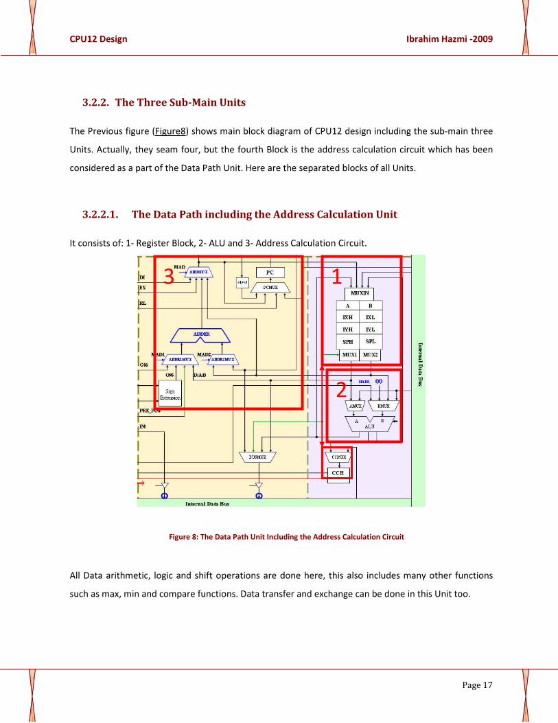
3.2.2. The Three Sub-Main Units
The Previous figure (Figure8) shows main block diagram of CPU12 design including the sub-main three
Units. Actually, they seam four, but the fourth Block is the address calculation circuit which has been
considered as a part of the Data Path Unit. Here are the separated blocks of all Units.
3.2.2.1. The Data Path including the Address Calculation Unit
It consists of: 1- Register Block, 2- ALU and 3- Address Calculation Circuit.
Figure 8: The Data Path Unit Including the Address Calculation Circuit
All Data arithmetic, logic and shift operations are done here, this also includes many other functions
such as max, min and compare functions. Data transfer and exchange can be done in this Unit too.
3 1
2
CPU12 Design Ibrahim Hazmi -2009
Page 18
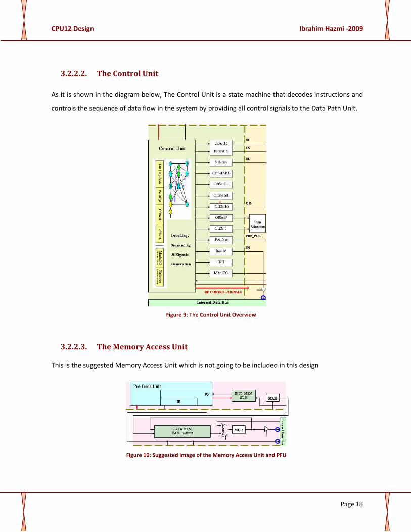
3.2.2.2. The Control Unit
As it is shown in the diagram below, The Control Unit is a state machine that decodes instructions and
controls the sequence of data flow in the system by providing all control signals to the Data Path Unit.
Figure 9: The Control Unit Overview
3.2.2.3. The Memory Access Unit
This is the suggested Memory Access Unit which is not going to be included in this design
Figure 10: Suggested Image of the Memory Access Unit and PFU
CPU12 Design Ibrahim Hazmi -2009
Page 19
4. Detailed Description of the design
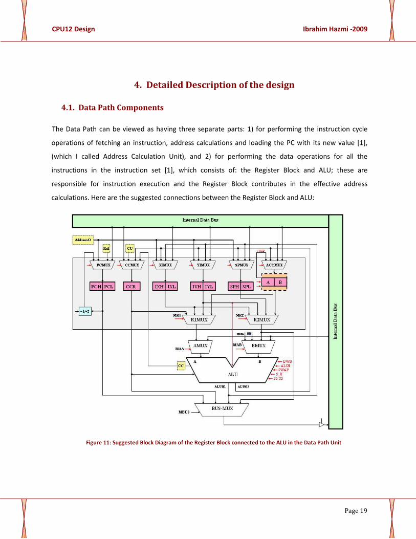
4.1. Data Path Components
The Data Path can be viewed as having three separate parts: 1) for performing the instruction cycle
operations of fetching an instruction, address calculations and loading the PC with its new value [1],
(which I called Address Calculation Unit), and 2) for performing the data operations for all the
instructions in the instruction set [1], which consists of: the Register Block and ALU; these are
responsible for instruction execution and the Register Block contributes in the effective address
calculations. Here are the suggested connections between the Register Block and ALU:
Figure 11: Suggested Block Diagram of the Register Block connected to the ALU in the Data Path Unit
CPU12 Design Ibrahim Hazmi -2009
Page 20
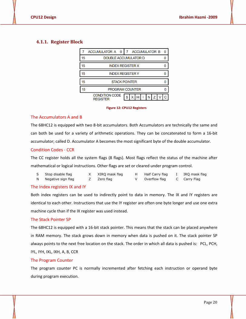
4.1.1. Register Block
Figure 12: CPU12 Registers
The Accumulators A and B
The 68HC12 is equipped with two 8-bit accumulators. Both Accumulators are technically the same and
can both be used for a variety of arithmetic operations. They can be concatenated to form a 16-bit
accumulator; called D. Accumulator A becomes the most significant byte of the double accumulator.
Condition Codes - CCR
The CC register holds all the system flags (8 flags). Most flags reflect the status of the machine after
mathematical or logical instructions. Other flags are set or cleared under program control.
S Stop disable flag X XIRQ mask flag H Half Carry flag I IRQ mask flag
N Negative sign flag Z Zero flag V Overflow flag C Carry Flag
The Index registers IX and IY
Both index registers can be used to indirectly point to data in memory. The IX and IY registers are
identical to each other. Instructions that use the IY register are often one byte longer and use one extra
machine cycle than if the IX register was used instead.
The Stack Pointer SP
The 68HC12 is equipped with a 16-bit stack pointer. This means that the stack can be placed anywhere
in RAM memory. The stack grows down in memory when data is pushed on it. The stack pointer SP
always points to the next free location on the stack. The order in which all data is pushed is: PCL, PCH,
IYL, IYH, IXL, IXH, A, B, CCR
The Program Counter
The program counter PC is normally incremented after fetching each instruction or operand byte
during program execution.
CPU12 Design Ibrahim Hazmi -2009
Page 21
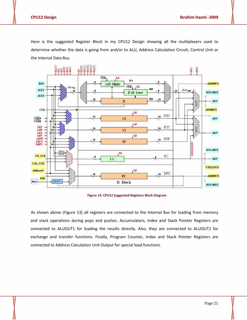
Here is the suggested Register Block in my CPU12 Design showing all the multiplexers used to
determine whether the data is going from and/or to ALU, Address Calculation Circuit, Control Unit or
the Internal Data Bus.
Figure 13: CPU12 Suggested Registers Block Diagram
As shown above (Figure 13) all registers are connected to the Internal Bus for loading from memory
and stack operations during pops and pushes. Accumulators, Index and Stack Pointer Registers are
connected to ALUOUT1 for loading the results directly. Also, they are connected to ALUOUT2 for
exchange and transfer functions. Finally, Program Counter, Index and Stack Pointer Registers are
connected to Address Calculation Unit Output for special load functions.

CPU12 Design Ibrahim Hazmi -2009
Page 22
4.1.1.1. Accumulators
Here is just extension to show how accumulators have been designed and how they are connected.
Figure 14: Accumulators A, B and D
These tables illustrate the mechanism of the Accumulators work. The Output should be one of the
followings: +/-:A, +/-:B and D (A:B). And the Input should either from the Accumulators output itself to
make the swap between A and B or from outside (ALU or BUS).
Table 1: Accumulators Logic
MI=SWAP IN_Mux LD
0 A:B A,B 1 SWAP A,B A,B
MDL B/AB MDH A/0F M0F OUT_Mux
0 AB 0 0F 0 (0) 00:A
0 AB 0 0F 1 (F) 11:A
1 B 0 0F 0 (0) 00:B
1 B 0 0F 1 (F) 11:B
1 B 1 A X D
MDL
MDH
0 0
1 MD
IN MUXDH/MUXDL ≠ 0/1 IF MDL =0 THEN MDH =0

CPU12 Design Ibrahim Hazmi -2009
Page 23
4.1.2. ALU Block
Figure 15: ALU Including Advanced Math (Multiplier and Divider)
As it can be shown Above, The ALU is Very Structural Circuit consisting of 16 instants of the Basic ALSU
to perform Parallel 16 bit Arithmetic, Logic and Shift Operations. It includes other circuitry such as 16-
bit Carry-look-ahead Generator (CLG) for fastening the operations, and Multiplication and Fast division
circuits for performing advanced mathematics. It also generates the Condition Code.
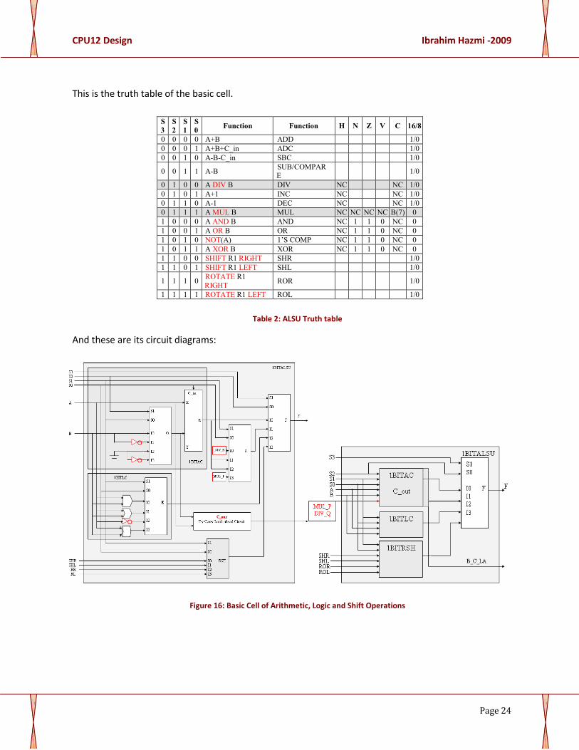
4.1.2.1. Basic Arithmetic, Logic and Shift (ALSU) Cell
The Basic Arithmetic, Logic and Shift (ALSU) Cell is simply a full adder and some Multiplexers. It could
be described well from the following table and diagram. The shaded rows in the table are for
multiplication and division selection. That has been done by ignoring the ability of transferring bits in
the ALSU Cell replacing it by transferring method which can be shown in the above figure (Figure 17).
CPU12 Design Ibrahim Hazmi -2009
Page 24
This is the truth table of the basic cell.
S3 S2 S1 S0
Function Function H N Z V C 16/8
0 0 0 0 A+B ADD 1/0 0 0 0 1 A+B+C_in ADC 1/0 0 0 1 0 A-B-C_in SBC 1/0
0 0 1 1 A-B SUB/COMPARE 1/0
0 1 0 0 A DIV B DIV NC NC 1/0 0 1 0 1 A+1 INC NC NC 1/0 0 1 1 0 A-1 DEC NC NC 1/0 0 1 1 1 A MUL B MUL NC NC NC NC B(7) 0 1 0 0 0 A AND B AND NC 1 1 0 NC 0 1 0 0 1 A OR B OR NC 1 1 0 NC 0 1 0 1 0 NOT(A) 1’S COMP NC 1 1 0 NC 0 1 0 1 1 A XOR B XOR NC 1 1 0 NC 0 1 1 0 0 SHIFT R1 RIGHT SHR 1/0 1 1 0 1 SHIFT R1 LEFT SHL 1/0
1 1 1 0 ROTATE R1 RIGHT ROR 1/0
1 1 1 1 ROTATE R1 LEFT ROL 1/0
Table 2: ALSU Truth table
And these are its circuit diagrams:
Figure 16: Basic Cell of Arithmetic, Logic and Shift Operations

CPU12 Design Ibrahim Hazmi -2009
Page 25
4.1.2.2. Address Calculation Unit
The Address Calculation Unit is also is included in the Data Path and responsible for effective address
calculation for Indexed and relative Addressing Modes. I am bringing Figure 8 here to show how
Address Calculation Unit works.
There are NO Address Calculations for Inherent, Immediate or Relative addressing modes. For Direct
and Extend addressing modes, there are two direct connections to the outer Address multiplexer as it is
shown above in the figure. The down circuit, which contains and adder and two multiplexers, is
designed to provide all calculations for Indexed Addressing Modes. The connection from Register Block
Multiplexer No.2 is for the Post Auto-Increment / Auto-Decrement Offset addressing, in which Index
and Stack Pointer Registers can be incremented/decremented after they contribute in the effective
address calculations.

CPU12 Design Ibrahim Hazmi -2009
Page 26
4.2. Control Unit
Program flow is dictated by the sequence of addresses written to the program counter. Sequential
execution of instructions is guaranteed by keeping track of bytes read by the instruction decoder. The
execute instructions module updates the program counter to account for branching, subroutine entry
and return instructions.
4.2.1. The Job of Control Unit
The job of my Control Unit is to decode the up-coming instruction from Instruction Register and apply
the right control signals to the Data Path Unit in the right sequence. decoding in the Decoding unit. In
Appendix A, there are some maps for the OpCode, which determines which is instruction is going to be
executed, and PostByte, which determines the Addressing mode. Here is the instruction Format with
some description of the PostByte
Figure 17: Instruction Format with Part of Decoding Unit
CPU12 Design Ibrahim Hazmi -2009
Page 27
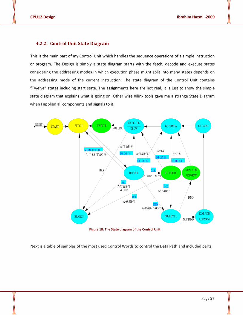
4.2.2. Control Unit State Diagram
This is the main part of my Control Unit which handles the sequence operations of a simple instruction
or program. The Design is simply a state diagram starts with the fetch, decode and execute states
considering the addressing modes in which execution phase might split into many states depends on
the addressing mode of the current instruction. The state diagram of the Control Unit contains
“Twelve” states including start state. The assignments here are not real. It is just to show the simple
state diagram that explains what is going on. Other wise Xilinx tools gave me a strange State Diagram
when I applied all components and signals to it.
RESET
NOT DIND
DIND
A='1' &B='1'
A='0'&A='1' &
A='0' &B='1'
BRA
NOT BRA
A='1' &B='1' &C='0'
A='0' &B='1' &C='1'
A='0' &B='0'
A='1'&B='0'
A='1'&B='1' &C='1'
A='0' & B='1'& C='0'
$18
DI OR EXIM OR IH
IM OR IH
REL
REL
IND
IND
DI OR EX
MORE FETCH
START RWRITE
POSTBYTE
P2DECODE
ICALADD
ADDMCW
GETDATA GETADDFETCHEXECUTE
DPCW
DECODEDCALADD
ADDMCW
BRANCH
Figure 18: The State diagram of the Control Unit
Next is a table of samples of the most used Control Words to control the Data Path and included parts.
CPU12 Design Ibrahim Hazmi -2009
Page 28
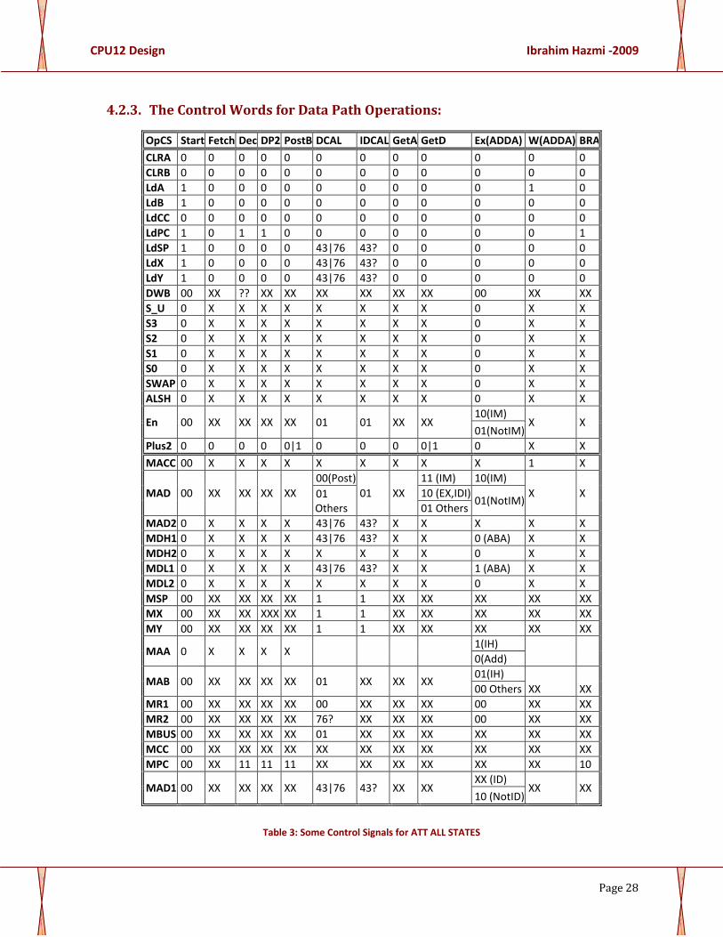
4.2.3. The Control Words for Data Path Operations:
Table 3: Some Control Signals for ATT ALL STATES
OpCS Start Fetch Dec DP2 PostB DCAL IDCAL GetA GetD Ex(ADDA) W(ADDA) BRA
CLRA 0 0 0 0 0 0 0 0 0 0 0 0 CLRB 0 0 0 0 0 0 0 0 0 0 0 0 LdA 1 0 0 0 0 0 0 0 0 0 1 0 LdB 1 0 0 0 0 0 0 0 0 0 0 0 LdCC 0 0 0 0 0 0 0 0 0 0 0 0 LdPC 1 0 1 1 0 0 0 0 0 0 0 1 LdSP 1 0 0 0 0 43|76 43? 0 0 0 0 0 LdX 1 0 0 0 0 43|76 43? 0 0 0 0 0 LdY 1 0 0 0 0 43|76 43? 0 0 0 0 0 DWB 00 XX ?? XX XX XX XX XX XX 00 XX XX S_U 0 X X X X X X X X 0 X X S3 0 X X X X X X X X 0 X X S2 0 X X X X X X X X 0 X X S1 0 X X X X X X X X 0 X X S0 0 X X X X X X X X 0 X X SWAP 0 X X X X X X X X 0 X X ALSH 0 X X X X X X X X 0 X X
En 00 XX XX XX XX 01 01 XX XX 10(IM)
X X 01(NotIM)
Plus2 0 0 0 0 0|1 0 0 0 0|1 0 X X
MACC 00 X X X X X X X X X 1 X
MAD 00 XX XX XX XX 00(Post)
01 XX 11 (IM) 10(IM)
X X 01 Others
10 (EX,IDI) 01(NotIM)
01 Others MAD2 0 X X X X 43|76 43? X X X X X MDH1 0 X X X X 43|76 43? X X 0 (ABA) X X MDH2 0 X X X X X X X X 0 X X MDL1 0 X X X X 43|76 43? X X 1 (ABA) X X MDL2 0 X X X X X X X X 0 X X MSP 00 XX XX XX XX 1 1 XX XX XX XX XX MX 00 XX XX XXX XX 1 1 XX XX XX XX XX MY 00 XX XX XX XX 1 1 XX XX XX XX XX
MAA 0 X X X X 1(IH)
0(Add)
MAB 00 XX XX XX XX 01 XX XX XX 01(IH)
XX XX 00 Others MR1 00 XX XX XX XX 00 XX XX XX 00 XX XX MR2 00 XX XX XX XX 76? XX XX XX 00 XX XX MBUS 00 XX XX XX XX 01 XX XX XX XX XX XX MCC 00 XX XX XX XX XX XX XX XX XX XX XX MPC 00 XX 11 11 11 XX XX XX XX XX XX 10
MAD1 00 XX XX XX XX 43|76 43? XX XX XX (ID)
XX XX 10 (NotID)

CPU12 Design Ibrahim Hazmi -2009
Page 29
Table 5: My Simulation Inputs and Some Expected Results
Next is the Result that I’ve obtained from my simulation using ModelSim PE Student Edition 6.5.
ADDMode LdSP LdY LdX MAD MAD1 MAD2 MDH1 MDL1 MR2 MAB MA
IH, IM, DI, EX 0 0 0 1 X X X X X X X
ID
O5 (rr) 76 76 76 0 10 r NAND r X X X X X
O9 (rr) 43 43 43 0 10 r NAND r X X X X X O16 (rr) 43 43 43 0 11 r NAND r X X X X X
PP (rr) 76 76 76 0 01 r NAND r X X 76? X 76? OA (rr) 43 43 43 0 00 r NAND r 0 0 X 0 X
OB (rr) 43 43 43 0 00 r NAND r 0 1 X 1 X
OD (rr) 43 43 43 0 00 r NAND r 1 1 X 1 X O16I (rr) 43 43 43 0 11 r NAND r X X X X X
ODI (rr) 43 43 43 0 00 r NAND r 1 1 X 1 X Table 4: Some Control Signals for different Addressing Modes
AddMode INSTSEL OPCODE POSTCODE ADD1 ADD2/IM DATA A
IH X X X X IM 0000 10001011 XXXXXXXX X 0000000010001000 88 00001000 DI 0001 10011011 XXXXXXXX 0000000000001000 X 1 00001001 EX 0010 10111011 XXXXXXXX 0000100000001000 X 2 00001011
ID
OFFSET5 0011 10101011 11010100 ? X 0 A OFFSET9 0100 10101011 11110000 1000000000010111 X 4 00001111
OFFSET16 0101 10101011 11110010 1000100000010111 X 5 00010100 PRE-POST 0110 10101011 00100010 1000000000010001 X 6 00011010 OFFSETA 0111 10101011 11101100 ? X 0 A OFFSETB 1000 10101011 11101101 ? X 0 A OFFSETD 1001 10101011 11100110 ? X 0 A
OFFSET16I 1010 10101011 11110011 1000000000010111 0000000000000101 8 00100010 OFFSETDI 1011 10101011 11101111 ? ? 0 A
DUMMY 1100 00011000 OpCodeP2 X X X 00110001
00000110
BUSDATA 1000000000001111 OFFSETH 00001000 mm 1000000000001111 OFFSETL 00001000 CU_CCR 10001111 REL8 00001001
A_0 10000100010000000 B 00001111

CPU12 Design Ibrahim Hazmi -2009
Page 30
4.3. Results (Timing Simulation)
1- IMM — Immediate (0000) 2- DIR — Direct (0001)
3- EXT — EXTEND (0010) 4- IDX: 5-bit constant offset from X, Y, SP, or PC (0011)

CPU12 Design Ibrahim Hazmi -2009
Page 31
5- IDX1 — 9-bit signed offset from X, Y, SP, or PC (0100)
6- IDX2 — 16-bit signed offset from X, Y, SP, or PC (0101)

CPU12 Design Ibrahim Hazmi -2009
Page 32
7- Pre/post increment/decrement by (10) (0110)

CPU12 Design Ibrahim Hazmi -2009
Page 33
8- Accumulator A OFFSET (0111) and Accumulator B offset (1000)
CPU12 Design Ibrahim Hazmi -2009
Page 34
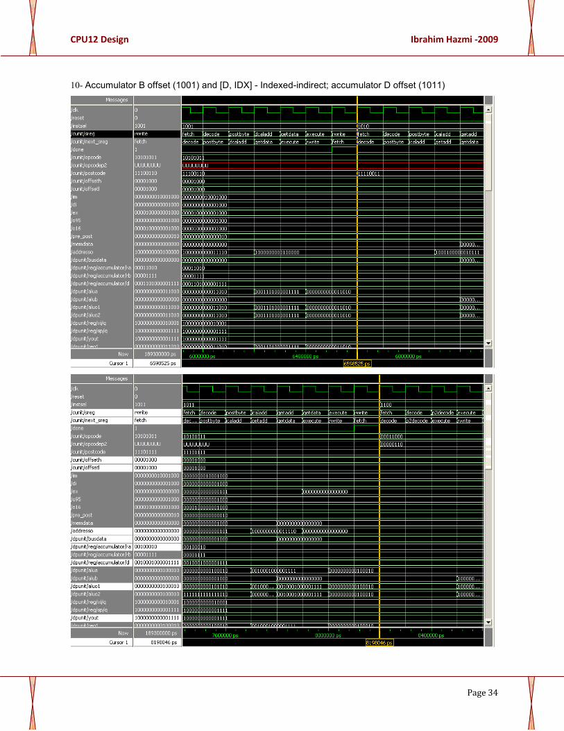
10- Accumulator B offset (1001) and [D, IDX] - Indexed-indirect; accumulator D offset (1011)
CPU12 Design Ibrahim Hazmi -2009
Page 35
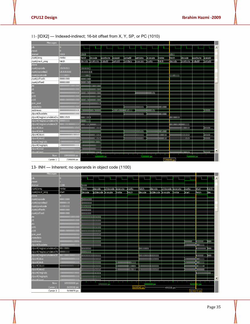
11- [IDX2] — Indexed-indirect; 16-bit offset from X, Y, SP, or PC (1010)
13- INH — Inherent; no operands in object code (1100)

CPU12 Design Ibrahim Hazmi -2009
Page 36
4.4. Project Outcomes: Evaluation (My Suggestions)
Cpu12 is designed and I suggest that It works at least (90-95)% as I’ve chosen samples of code and
there was some doubt of having little mistakes with some results obtained in the Timing
Simulation Diagram in the
• A Block Diagram of the whole Design and partitioned it to 5 Main Blocks, Designed and coded
Data Path. (all ALU REG Blocks), Designed some parts of the Control Unit (CU), Put the main
parts of the Pre-Fetch Unit (PFU). (95%)
• Design Cpu12 and make it works properly for the selected samples of its instruction set and
this will be met by designing the following:
o Data Path Unit which consist of
§ Register Block housing all CPU12 internal registers (100%)
• Accumulators A, B and D(A:B)
• Index registers X and Y
• Stack Pointer (SP) and Program Counter (PC)
• Condition Code Register (CC) – ALU sensor and Control Unit input
§ ALU, Arithmetic, Logic and Shift unit which does all data manipulations where
data could come from registers or memory. This includes (95%) (CCR!)
• Designing a basic cell for all simple ALU operations, and
• Extra Circuits to gain more operations and obtain the right condition
Code results for all operations
• Advanced Mathematical Circuits for Multiplication and Division
§ Address Calculation Circuit connected to Register Block and ALU to provide
accurate effective address for all addressing modes. (100%)
o Control Unit which is, again, a simple state diagram shows all possible states that
include all addressing modes. (80%)
• Combining the Two Parts together. (100%)
• Simulation (Test Bench and Timing Diagrams) (90%)
CPU12 Design Ibrahim Hazmi -2009
Page 37
Conclusions
To summarize, the following are some points that come out from the work that has been done on the
design of the CPU12:
• The Project was aiming to design the tow units of the CPU12, (Data Path and Control Unit),
individually then combine them together to run a simple sequence of instructions. Additional
challenge is to make the design as structural as it possible and behavioral Level where it needs
to be and that has been satisfied for the Data Path Unit whereas Control unit was designed as a
state machine which is totally in behavioral Level.
• There were many trials to come out with final Data Path Unit circuits. For instance, the Register
block has been designed several times and in different considerations. At the beginning, it was a
separate block diagram that is not specifically designed for CPU12. But then it has been changed
to fit CPU12 needs and other parts connections with the registers inside. Accumulator is simple,
but it has been changed many times to insure that it produces the right data at the right time by
applying the right control.
• AT the Beginning, I was taking every part of Micro as a separate part and design it without any
guidelines except its functionality, which was bringing difficulty to join all parts together at the
end. Also it was leading me to put unnecessary circuits into it.
• The answer of the question: What is the first thing I should know in doing such design was the
key of the understanding and imagination of what id going on. It leads, at then end, to draw a
reasonable block diagram that meets the requirements.
• The Idea of Partitioning was behind the ability to design CPU12 block by block considering the
relations between all blocks and the targeted instruction set. Before, it was wasting of time
thinking of everything at the same time.
• During my work in this design, I’ve got the Idea of starting with the simplest then improve the
Design based on thinking, reading and people additions.
• I’ve gained a good understanding of how embedded systems work, how to manage the
Microcontrollers processes and how to connect its parts together in order to run a simple code.
• Practicing the design was more difficult than imagining the ability to do.

CPU12 Design Ibrahim Hazmi -2009
Page 38
References
1. Enoch O. Hwang, 2005, Digital Logic and Microprocessor Design With VHDL, La Sierra University,
Riverside, USA.
2. Altera Co, 2009, AN 311: Standard Cell ASIC to FPGA Design, Methodology and Guidelines
3. E. Ostúa, J. Juan Chico, J. Viejo, M. J. Bellido, D. Guerrero, A. Millán & P. Ruiz-de-Clavijo, A SOC
DESIGN METHODOLOGY FOR LEON2 ON FPGA, Universidad de Sevilla.
4. Volnei A. Pedroni, 2004, Circuit Design with VHDL, MIT Press, Cambridge, Massachusetts,
London, England
5. PONG P. CHU, 2006, RTL HARDWARE DESIGN USING VHDL, Cleveland State University, WlLEY
INTERSCIENCE.
6. Peter J. Ashenden, 1990, The VHDL Cookbook, Dept. Computer Science, University of Adelaide,
SA, 1ST Edition
7. M. Morris Mano, 1993, Computer System Architecture, 3rd Edition, Prentice Hall Int.
8. Digitaaltehnika erikursus, Digital Design Methodology
9. Freescale Semiconductor, 2006, CPU12 Reference Manual (CPU12RM); Motorola M68HC12 and
HCS12 Microcontrollers, Rev. 4.0
10. HC11: http://online.sfsu.edu/~valverde/ENGR/ENGR478_s07/welcome.htm, Dr. Ricardo V., 2004,
Lcture Notes; ENGR 478,
11. LC3: http://www.et.byu.edu/groups/ece224web/lectures/LC3-2.pdf, 20/07/2009
12. http://www.eng.auburn.edu/~nelson/, 13/03/2009.
13. http://oucsace.cs.ohiou.edu/~avinashk/, 13/03/2009.
14. http://cs.lasierra.edu/~ehwang/mybook/toc.html, 13/03/2009.
15. http://lap2.epfl.ch/courses/archord1/, 13/03/2009.
16. http://www.ece.tamu.edu/~vinith/ecen248/index_files/lab_manual_spring09.pdf, 13/03/2009
17. http://www.eda-stds.org/rassp/, 13/03/2009.
18. http://vlsi.ee.hacettepe.edu.tr/links.html, 13/03/2009.
19. Reto Z., 1999, Lecture notes on Computer Arithmetic: Principles, Architectures, and VLSI Design,
Integrated Systems Laboratory, Swiss Federal Institute of Technology (ETH), Switzerland.

CPU12 Design Ibrahim Hazmi -2009
Page 39
Appendices
AAppppeennddiixx AA:: UUsseeffuull TTaabblleess ffoorr HHCC1122 [[99]]
HHCC1122 AAddddrreessssiinngg MMooddeess::

CPU12 Design Ibrahim Hazmi -2009
Page 40
CCPPUU1122 OOPPCCOODDEE MMaapp PPaaggee11::

CPU12 Design Ibrahim Hazmi -2009
Page 41
CCPPUU1122 OOPPCCOODDEE MMaapp PPaaggee22::
CPU12 Design Ibrahim Hazmi -2009
Page 42
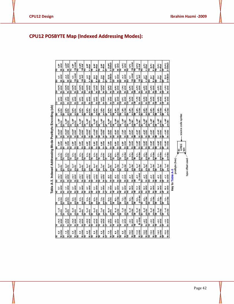
CCPPUU1122 PPOOSSBBYYTTEE MMaapp ((IInnddeexxeedd AAddddrreessssiinngg MMooddeess))::
CPU12 Design Ibrahim Hazmi -2009
Page 43
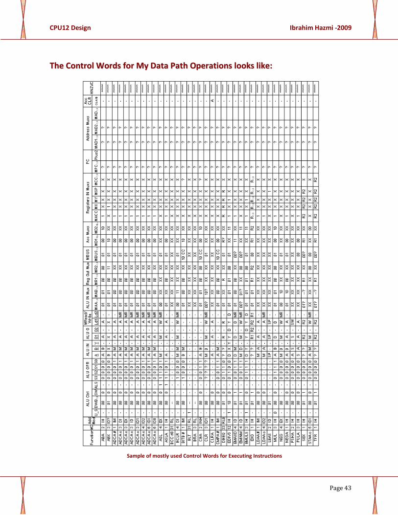
TThhee CCoonnttrrooll WWoorrddss ffoorr MMyy DDaattaa PPaatthh OOppeerraattiioonnss llooookkss lliikkee::
Sample of mostly used Control Words for Executing Instructions
CPU12 Design Ibrahim Hazmi -2009
Page 44
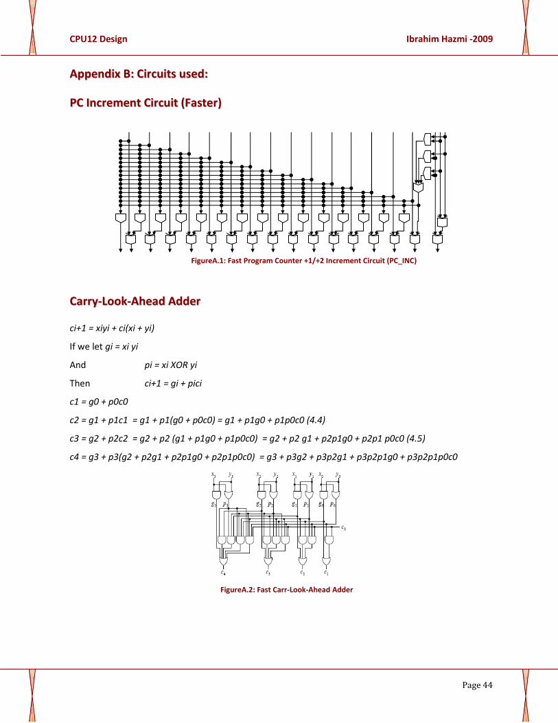
AAppppeennddiixx BB:: CCiirrccuuiittss uusseedd::
PPCC IInnccrreemmeenntt CCiirrccuuiitt ((FFaasstteerr))
FigureA.1: Fast Program Counter +1/+2 Increment Circuit (PC_INC)
CCaarrrryy--LLooookk--AAhheeaadd AAddddeerr
ci+1 = xiyi + ci(xi + yi)
If we let gi = xi yi
And pi = xi XOR yi
Then ci+1 = gi + pici
c1 = g0 + p0c0
c2 = g1 + p1c1 = g1 + p1(g0 + p0c0) = g1 + p1g0 + p1p0c0 (4.4)
c3 = g2 + p2c2 = g2 + p2 (g1 + p1g0 + p1p0c0) = g2 + p2 g1 + p2p1g0 + p2p1 p0c0 (4.5)
c4 = g3 + p3(g2 + p2g1 + p2p1g0 + p2p1p0c0) = g3 + p3g2 + p3p2g1 + p3p2p1g0 + p3p2p1p0c0
FigureA.2: Fast Carr-Look-Ahead Adder
CPU12 Design Ibrahim Hazmi -2009
Page 45
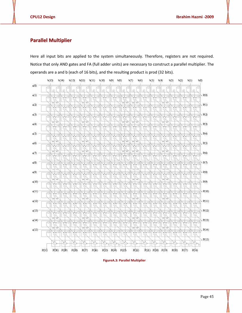
PPaarraalllleell MMuullttiipplliieerr
Here all input bits are applied to the system simultaneously. Therefore, registers are not required.
Notice that only AND gates and FA (full adder units) are necessary to construct a parallel multiplier. The
operands are a and b (each of 16 bits), and the resulting product is prod (32 bits).
FigureA.3: Parallel Multiplier

CPU12 Design Ibrahim Hazmi -2009
Page 46
3322//1177 BBiitt DDiivviiddeerr :: NNoonn--RReessttoorriinngg ((FFaasstt DDiivviiddeerr))
Figure A.4: Fast Divider
a14
a13
a12
a11
a10
a9
a8
a7
a6
a5
a4
a3
a2
a1
a0
q15
q14
q13
q12
q11
q10
q9
q8
q7
q6
q5
q4
q3
q2
q1
q0
b15 a30 b14 a29 b13 a28 b12 a27 b11 a26 b10 a25 b9 a24 b8 a23 b7 a22 b6 a21 b5 a20 b4 a19 b3 a18 b2 a17 b1 a16 b0 a15
r15 r14 r13 r12 r11 r10 r9 r8 r7 r6 r5 r4 r3 r2 r1 r0
a30 ⊕ b15
CPU12 Design Ibrahim Hazmi -2009
Page 47
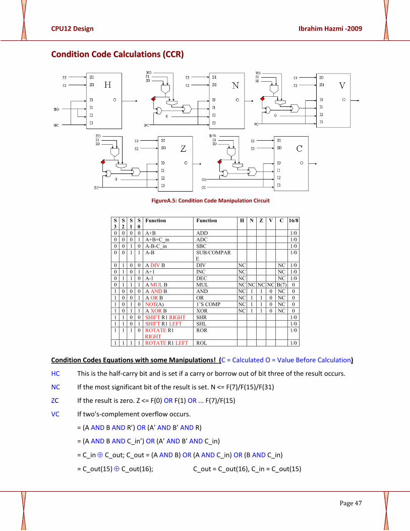
CCoonnddiittiioonn CCooddee CCaallccuullaattiioonnss ((CCCCRR))
FigureA.5: Condition Code Manipulation Circuit
S3 S2 S1 S0 Function Function H N Z V C 16/8
0 0 0 0 A+B ADD 1/0 0 0 0 1 A+B+C_in ADC 1/0 0 0 1 0 A-B-C_in SBC 1/0 0 0 1 1 A-B SUB/COMPAR
E 1/0
0 1 0 0 A DIV B DIV NC NC 1/0 0 1 0 1 A+1 INC NC NC 1/0 0 1 1 0 A-1 DEC NC NC 1/0 0 1 1 1 A MUL B MUL NC NC NC NC B(7) 0 1 0 0 0 A AND B AND NC 1 1 0 NC 0 1 0 0 1 A OR B OR NC 1 1 0 NC 0 1 0 1 0 NOT(A) 1’S COMP NC 1 1 0 NC 0 1 0 1 1 A XOR B XOR NC 1 1 0 NC 0 1 1 0 0 SHIFT R1 RIGHT SHR 1/0 1 1 0 1 SHIFT R1 LEFT SHL 1/0 1 1 1 0 ROTATE R1
RIGHT ROR 1/0
1 1 1 1 ROTATE R1 LEFT ROL 1/0
Condition Codes Equations with some Manipulations! (C = Calculated O = Value Before Calculation)
HC This is the half-carry bit and is set if a carry or borrow out of bit three of the result occurs.
NC If the most significant bit of the result is set. N <= F(7)/F(15)/F(31)
ZC If the result is zero. Z <= F(0) OR F(1) OR ... F(7)/F(15)
VC If two's-complement overflow occurs.
= (A AND B AND R’) OR (A’ AND B’ AND R)
= (A AND B AND C_in’) OR (A’ AND B’ AND C_in)
= C_in ⊕ C_out; C_out = (A AND B) OR (A AND C_in) OR (B AND C_in)
= C_out(15) ⊕ C_out(16); C_out = C_out(16), C_in = C_out(15)
CPU12 Design Ibrahim Hazmi -2009
Page 48
CC If a carry or borrow occurs. C <= C_out(16)
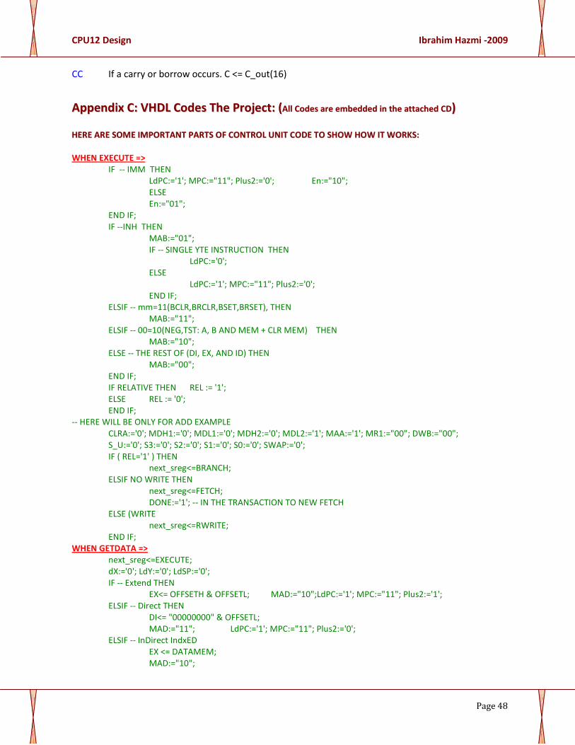
AAppppeennddiixx CC:: VVHHDDLL CCooddeess TThhee PPrroojjeecctt:: ((AAllll CCooddeess aarree eemmbbeeddddeedd iinn tthhee aattttaacchheedd CCDD))
HHEERREE AARREE SSOOMMEE IIMMPPOORRTTAANNTT PPAARRTTSS OOFF CCOONNTTRROOLL UUNNIITT CCOODDEE TTOO SSHHOOWW HHOOWW IITT WWOORRKKSS:: WHEN EXECUTE =>
IF -- IMM THEN LdPC:='1'; MPC:="11"; Plus2:='0'; En:="10"; ELSE En:="01";
END IF; IF --INH THEN MAB:="01"; IF -- SINGLE YTE INSTRUCTION THEN LdPC:='0'; ELSE LdPC:='1'; MPC:="11"; Plus2:='0'; END IF; ELSIF -- mm=11(BCLR,BRCLR,BSET,BRSET), THEN
MAB:="11"; ELSIF -- 00=10(NEG,TST: A, B AND MEM + CLR MEM) THEN
MAB:="10"; ELSE -- THE REST OF (DI, EX, AND ID) THEN MAB:="00"; END IF; IF RELATIVE THEN REL := '1'; ELSE REL := '0'; END IF; -- HERE WILL BE ONLY FOR ADD EXAMPLE CLRA:='0'; MDH1:='0'; MDL1:='0'; MDH2:='0'; MDL2:='1'; MAA:='1'; MR1:="00"; DWB:="00"; S_U:='0'; S3:='0'; S2:='0'; S1:='0'; S0:='0'; SWAP:='0';
IF ( REL='1' ) THEN next_sreg<=BRANCH; ELSIF NO WRITE THEN next_sreg<=FETCH; DONE:='1'; -- IN THE TRANSACTION TO NEW FETCH ELSE (WRITE
next_sreg<=RWRITE; END IF; WHEN GETDATA => next_sreg<=EXECUTE; dX:='0'; LdY:='0'; LdSP:='0'; IF -- Extend THEN EX<= OFFSETH & OFFSETL; MAD:="10";LdPC:='1'; MPC:="11"; Plus2:='1'; ELSIF -- Direct THEN DI<= "00000000" & OFFSETL; MAD:="11"; LdPC:='1'; MPC:="11"; Plus2:='0'; ELSIF -- InDirect IndxED EX <= DATAMEM; MAD:="10";
CPU12 Design Ibrahim Hazmi -2009
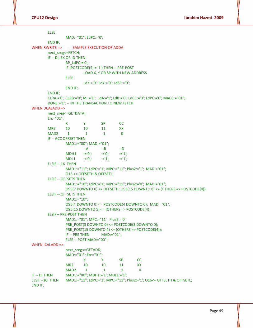
Page 49
ELSE MAD:="01"; LdPC:='0'; END IF; WHEN RWRITE => -- SAMPLE EXECUTION OF ADDA next_sreg<=FETCH; IF -- DI, EX OR ID THEN BP_LdPC:='0'; IF (POSTCODE(5) = '1') THEN -- PRE-POST LOAD X, Y OR SP WITH NEW ADDRESS
ELSE LdX:='0'; LdY:='0'; LdSP:='0'; END IF; END IF;
CLRA:='0'; CLRB:='0'; MI:='1'; LdA:='1'; LdB:='0'; LdCC:='0'; LdPC:='0'; MACC:="01"; DONE:='1'; -- IN THE TRANSACTION TO NEW FETCH WHEN DCALADD => next_sreg<=GETDATA; En:="01"; X Y SP CC MR2 10 10 11 XX MAD2 1 1 1 0 IF -- ACC OFFSET THEN MAD1:="00"; MAD:="01"; --A --B --D MDH1 :='0'; :='0'; :='1'; MDL1 :='0'; :='1'; :='1'; ELSIF -- 16 THEN MAD1:="11"; LdPC:='1'; MPC:="11"; Plus2:='1'; MAD:="01"; O16 <= OFFSETH & OFFSETL; ELSIF -- OFFSET9 THEN MAD1:="10"; LdPC:='1'; MPC:="11"; Plus2:='0'; MAD:="01"; O95(7 DOWNTO 0) <= OFFSETH; O95(15 DOWNTO 8) <= (OTHERS => POSTCODE(0));
ELSIF -- OFFSET5 THEN MAD1:="10"; O95(4 DOWNTO 0) <= POSTCODE(4 DOWNTO 0); MAD:="01"; O95(15 DOWNTO 5) <= (OTHERS => POSTCODE(4));
ELSIF – PRE-POST THEN MAD1:="01"; MPC:="11"; Plus2:='0'; PRE_POST(3 DOWNTO 0) <= POSTCODE(3 DOWNTO 0); PRE_POST(15 DOWNTO 4) <= (OTHERS => POSTCODE(4)); IF -- PRE THEN MAD:="01";
ELSE -- POST MAD:="00"; WHEN ICALADD => next_sreg<=GETADD; MAD:="01"; En:="01"; X Y SP CC MR2 10 10 11 XX MAD2 1 1 1 0 IF -- DI THEN MAD1:="00"; MDH1:='1'; MDL1:='1'; ELSIF –16I THEN MAD1:="11"; LdPC:='1'; MPC:="11"; Plus2:='1'; O16<= OFFSETH & OFFSETL; END IF;