hc12 cpu12 reference manual
DESCRIPTION
s12TRANSCRIPT

Order this document byCPU12RM/AD
Rev. 1.0
NO
N-
DI
SC
LO
SU
RE
A
GR
EE
ME
NT
R
EQ
UI
RE
D
CPU12Reference Manual
HC12HC12HC12

N
ON
-D
IS
CL
OS
UR
E
AG
RE
EM
EN
T
RE
QU
IR
ED
Motorola reserves the right to make changes without further notice toany products herein to improve reliability, function or design. Motoroladoes not assume any liability arising out of the application or use of anyproduct or circuit described herein; neither does it convey any licenseunder its patent rights nor the rights of others. Motorola products are notdesigned, intended, or authorized for use as components in systemsintended for surgical implant into the body, or other applications intendedto support or sustain life, or for any other application in which the failureof the Motorola product could create a situation where personal injury ordeath may occur. Should Buyer purchase or use Motorola products forany such unintended or unauthorized application, Buyer shall indemnifyand hold Motorola and its officers, employees, subsidiaries, affiliates,and distributors harmless against all claims, costs, damages, andexpenses, and reasonable attorney fees arising out of, directly orindirectly, any claim of personal injury or death associated with suchunintended or unauthorized use, even if such claim alleges that Motorolawas negligent regarding the design or manufacture of the part.

TABLE OF CONTENTS
Paragraph Page
SECTION 1INTRODUCTION
1.1 CPU12 Features .............................................................................................. 1-11.2 Readership....................................................................................................... 1-11.3 Symbols and Notation ...................................................................................... 1-2
SECTION 2OVERVIEW
2.1 Programming Model......................................................................................... 2-12.2 Data Types....................................................................................................... 2-52.3 Memory Organization....................................................................................... 2-52.4 Instruction Queue............................................................................................. 2-5
SECTION 3ADDRESSING MODES
3.1 Mode Summary................................................................................................ 3-13.2 Effective Address ............................................................................................. 3-23.3 Inherent Addressing Mode............................................................................... 3-23.4 Immediate Addressing Mode ........................................................................... 3-23.5 Direct Addressing Mode................................................................................... 3-33.6 Extended Addressing Mode............................................................................. 3-33.7 Relative Addressing Mode ............................................................................... 3-43.8 Indexed Addressing Modes.............................................................................. 3-53.9 Instructions Using Multiple Modes ................................................................. 3-103.10 Addressing More than 64 Kbytes ................................................................... 3-12
SECTION 4INSTRUCTION QUEUE
4.1 Queue Description ........................................................................................... 4-14.2 Data Movement in the Queue .......................................................................... 4-24.3 Changes in Execution Flow.............................................................................. 4-2
SECTION 5INSTRUCTION SET OVERVIEW
5.1 Instruction Set Description ............................................................................... 5-15.2 Load and Store Instructions ............................................................................. 5-15.3 Transfer and Exchange Instructions ................................................................ 5-25.4 Move Instructions ............................................................................................. 5-35.5 Addition and Subtraction Instructions............................................................... 5-35.6 Binary Coded Decimal Instructions .................................................................. 5-45.7 Decrement and Increment Instructions ............................................................ 5-45.8 Compare and Test Instructions ........................................................................ 5-55.9 Boolean Logic Instructions ............................................................................... 5-65.10 Clear, Complement, and Negate Instructions .................................................. 5-6
CPU12 MOTOROLA
REFERENCE MANUAL iii

Paragraph Page
TABLE OF CONTENTS
5.11 Multiplication and Division Instructions ............................................................ 5-75.12 Bit Test and Manipulation Instructions ............................................................. 5-75.13 Shift and Rotate Instructions ............................................................................ 5-85.14 Fuzzy Logic Instructions................................................................................... 5-95.15 Maximum and Minimum Instructions.............................................................. 5-115.16 Multiply and Accumulate Instruction............................................................... 5-115.17 Table Interpolation Instructions ...................................................................... 5-125.18 Branch Instructions ........................................................................................ 5-135.19 Loop Primitive Instructions ............................................................................. 5-165.20 Jump and Subroutine Instructions.................................................................. 5-175.21 Interrupt Instructions ...................................................................................... 5-185.22 Index Manipulation Instructions...................................................................... 5-195.23 Stacking Instructions ...................................................................................... 5-205.24 Pointer and Index Calculation Instructions..................................................... 5-205.25 Condition Code Instructions ........................................................................... 5-215.26 STOP and WAIT Instructions ......................................................................... 5-215.27 Background Mode and Null Operations ......................................................... 5-22
SECTION 6INSTRUCTION GLOSSARY
6.1 Glossary Information ........................................................................................ 6-16.2 Condition Code Changes ................................................................................. 6-26.3 Object Code Notation....................................................................................... 6-26.4 Source Forms................................................................................................... 6-36.5 Cycle-by-Cycle Execution ................................................................................ 6-56.6 Glossary ........................................................................................................... 6-8
SECTION 7EXCEPTION PROCESSING
7.1 Types of Exceptions......................................................................................... 7-17.2 Exception Priority ............................................................................................. 7-27.3 Resets .............................................................................................................. 7-27.4 Interrupts .......................................................................................................... 7-37.5 Unimplemented Opcode Trap .......................................................................... 7-57.6 Software Interrupt Instruction ........................................................................... 7-67.7 Exception Processing Flow.............................................................................. 7-6
SECTION 8DEVELOPMENT AND DEBUG SUPPORT
8.1 External Reconstruction of the Queue ............................................................. 8-18.2 Instruction Queue Status Signals..................................................................... 8-18.3 Implementing Queue Reconstruction............................................................... 8-38.4 Background Debug Mode ................................................................................ 8-68.5 Instruction Tagging......................................................................................... 8-13
MOTOROLA CPU12
iv REFERENCE MANUAL
Paragraph Page
TABLE OF CONTENTS
8.6 Breakpoints .................................................................................................... 8-14
SECTION 9FUZZY LOGIC SUPPORT
9.1 Introduction ...................................................................................................... 9-19.2 Fuzzy Logic Basics .......................................................................................... 9-19.3 Example Inference Kernel................................................................................ 9-79.4 MEM Instruction Details ................................................................................... 9-99.5 REV, REVW Instruction Details ..................................................................... 9-139.6 WAV Instruction Details ................................................................................. 9-229.7 Custom Fuzzy Logic Programming ................................................................ 9-26
SECTION 10MEMORY EXPANSION
10.1 Expansion System Description ...................................................................... 10-110.2 CALL and Return from Call Instructions......................................................... 10-310.3 Address Lines for Expansion Memory ........................................................... 10-410.4 Overlay Window Controls............................................................................... 10-410.5 Using Chip-Select Circuits ............................................................................. 10-510.6 System Notes................................................................................................. 10-7
APPENDIX AINSTRUCTION REFERENCE
A.1 Instruction Set Summary..................................................................................A-1A.2 Opcode Map.....................................................................................................A-1A.3 Indexed Addressing Postbyte Encoding ..........................................................A-1A.4 Transfer and Exchange Postbyte Encoding.....................................................A-1A.5 Loop Primitive Postbyte Encoding ...................................................................A-1
APPENDIX BM68HC11 TO M68HC12 UPGRADE PATH
B.1 CPU12 Design Goals .......................................................................................B-1B.2 Source Code Compatibility...............................................................................B-1B.3 Programmer’s Model and Stacking ..................................................................B-3B.4 True 16-Bit Architecture ...................................................................................B-3B.5 Improved Indexing............................................................................................B-6B.6 Improved Performance.....................................................................................B-9B.7 Additional Functions.......................................................................................B-11
APPENDIX CHIGH-LEVEL LANGUAGE SUPPORT
C.1 Data Types...................................................................................................... C-1C.2 Parameters and Variables............................................................................... C-1C.3 Increment and Decrement Operators.............................................................. C-3
CPU12 MOTOROLA
REFERENCE MANUAL v

Paragraph Page
TABLE OF CONTENTS
C.4 Higher Math Functions .................................................................................... C-3C.5 Conditional If Constructs ................................................................................. C-4C.6 Case and Switch Statements .......................................................................... C-4C.7 Pointers ........................................................................................................... C-4C.8 Function Calls ................................................................................................. C-4C.9 Instruction Set Orthogonality........................................................................... C-5
APPENDIX DASSEMBLY LISTING
INDEX
SUMMARY OF CHANGES
MOTOROLA CPU12
vi REFERENCE MANUAL

LIST OF ILLUSTRATIONS
Figure Page
2-1 Programming Model......................................................................................... 2-16-1 Example Glossary Page................................................................................... 6-17-2 Exception Processing Flow Diagram ............................................................... 7-78-1 Queue Status Signal Timing ............................................................................ 8-28-2 BDM Host to Target Serial Bit Timing .............................................................. 8-88-3 BDM Target to Host Serial Bit Timing (Logic 1) ............................................... 8-88-4 BDM Target to Host Serial Bit Timing (Logic 0) ............................................... 8-98-5 Tag Input Timing ............................................................................................ 8-139-1 Block Diagram of a Fuzzy Logic System.......................................................... 9-39-2 Fuzzification Using Membership Functions...................................................... 9-49-3 Fuzzy Inference Engine ................................................................................... 9-89-4 Defining a Normal Membership Function....................................................... 9-109-5 MEM Instruction Flow Diagram...................................................................... 9-119-6 Abnormal Membership Function Case 1........................................................ 9-129-7 Abnormal Membership Function Case 2........................................................ 9-139-8 Abnormal Membership Function Case 3........................................................ 9-139-9 REV Instruction Flow Diagram....................................................................... 9-169-10 REVW Instruction Flow Diagram.................................................................... 9-219-11 WAV and wavr Instruction Flow Diagram....................................................... 9-259-12 Endpoint Table Handling................................................................................ 9-28
CPU12 MOTOROLA
REFERENCE MANUAL vii

MOTOROLA CPU12
viii REFERENCE MANUAL

LIST OF TABLES
Table Page
3-1 M68HC12 Addressing Mode Summary............................................................ 3-13-2 Summary of Indexed Operations ..................................................................... 3-63-3 PC Offsets for Move Instructions ................................................................... 3-115-1 Load and Store Instructions ............................................................................. 5-25-2 Transfer and Exchange Instructions ................................................................ 5-35-3 Move Instructions ............................................................................................. 5-35-4 Addition and Subtraction Instructions............................................................... 5-45-5 BCD Instructions .............................................................................................. 5-45-6 Decrement and Increment Instructions ............................................................ 5-55-7 Compare and Test Instructions ........................................................................ 5-55-8 Boolean Logic Instructions ............................................................................... 5-65-9 Clear, Complement, and Negate Instructions .................................................. 5-65-10 Multiplication and Division Instructions ............................................................ 5-75-11 Bit Test and Manipulation Instructions ............................................................. 5-75-12 Shift and Rotate Instructions ............................................................................ 5-85-13 Fuzzy Logic Instructions................................................................................. 5-105-14 Minimum and Maximum Instructions.............................................................. 5-115-15 Multiply and Accumulate Instructions............................................................. 5-125-16 Table Interpolation Instructions ...................................................................... 5-125-17 Short Branch Instructions............................................................................... 5-145-18 Long Branch Instructions ............................................................................... 5-155-19 Bit Condition Branch Instructions ................................................................... 5-165-20 Loop Primitive Instructions ............................................................................. 5-165-21 Jump and Subroutine Instructions.................................................................. 5-175-22 Interrupt Instructions ...................................................................................... 5-185-23 Index Manipulation Instructions...................................................................... 5-195-24 Stacking Instructions ...................................................................................... 5-205-25 Pointer and Index Calculation Instructions..................................................... 5-215-26 Condition Codes Instructions ......................................................................... 5-215-27 STOP and WAIT Instructions ......................................................................... 5-225-28 Background Mode and Null Operation Instructions........................................ 5-227-1 CPU12 Exception Vector Map ......................................................................... 7-17-2 Stacking Order on Entry to Interrupts............................................................... 7-58-1 IPIPE[1:0] Decoding......................................................................................... 8-28-2 BDM Commands Implemented in Hardware.................................................. 8-108-3 BDM Firmware Commands............................................................................ 8-118-4 BDM Register Mapping .................................................................................. 8-118-5 Tag Pin Function ............................................................................................ 8-1310-1 Mapping Precedence ..................................................................................... 10-2A-1 Instruction Set Summary..................................................................................A-2A-2 CPU12 Opcode Map......................................................................................A-20A-3 Indexed Addressing Mode Summary .............................................................A-22A-4 Indexed Addressing Mode Postbyte Encoding (xb) .......................................A-23
CPU12 MOTOROLA
REFERENCE MANUAL ix
LIST OF TABLES
A-5 Transfer and Exchange Postbyte Encoding...................................................A-24A-6 Loop Primitive Postbyte Encoding (lb) ...........................................................A-25B-1 Translated M68HC11 Mnemonics....................................................................B-2B-2 Instructions with Smaller Object Code .............................................................B-3B-3 Comparison of Math Instruction Speeds ........................................................B-10B-4 New M68HC12 Instructions ...........................................................................B-11
MOTOROLA CPU12
x REFERENCE MANUAL

SECTION 1INTRODUCTION
This manual describes the features and operation of the CPU12 processing unit usedin all M68HC12 microcontrollers.
1.1 CPU12 Features
The CPU12 is a high-speed, 16-bit processing unit that has a programming modelidentical to that of the industry standard M68HC11 CPU. The CPU12 instruction set isa proper superset of the M68HC11 instruction set, and M68HC11 source code is ac-cepted by CPU12 assemblers with no changes.
The CPU12 has full 16-bit data paths and can perform arithmetic operations up to 20bits wide for high-speed math execution.
Unlike many other 16-bit CPUs, the CPU12 allows instructions with odd byte counts,including many single-byte instructions. This allows much more efficient use of ROMspace.
An instruction queue buffers program information so the CPU has immediate accessto at least three bytes of machine code at the start of every instruction.
In addition to the addressing modes found in other Motorola MCUs, the CPU12 offersan extensive set of indexed addressing capabilities including:
• Using the stack pointer as an index register in all indexed operations• Using the program counter as an index register in all but auto inc/dec mode• Accumulator offsets allowed using A, B, or D accumulators• Automatic pre- or post-increment or pre- or post-decrement (by –8 to +8)• 5-bit, 9-bit, or 16-bit signed constant offsets• 16-bit offset indexed-indirect and accumulator D offset indexed-indirect ad-
dressing
1.2 Readership
This manual is written for professionals and students in electronic design and softwaredevelopment. The primary goal is to provide information necessary to implement con-trol systems using M68HC12 devices. Basic knowledge of electronics, microproces-sors, and assembly language programming is required to use the manual effectively.Because the CPU12 has a great deal of commonality with the M68HC11 CPU, priorknowledge of M68HC11 devices is helpful, but is not essential. The CPU12 also in-cludes features that are new and unique. In these cases, there is supplementary ma-terial in the text to explain the new technology.
CPU12 INTRODUCTION MOTOROLA
REFERENCE MANUAL 1-1

1.3 Symbols and Notation
The following symbols and notation are used throughout the manual. More specializedusages that apply only to the instruction glossary are described at the beginning of thatsection.
1.3.1 Abbreviations for System Resources
1.3.2 Memory and Addressing
A — Accumulator AB — Accumulator BD — Double accumulator D (A : B)X — Index register XY — Index register Y
SP — Stack pointerPC — Program counter
CCR — Condition code registerS – STOP instruction control bitX– Non-maskable interrupt control bitH – Half-carry status bitI – Maskable interrupt control bitN – Negative status bitZ – Zero status bitV – Two’s complement overflow status bitC – Carry/Borrow status bit
M — 8-bit memory location pointed to by the effective address of the in-struction
M : M+1 — 16-bit memory location. Consists of the location pointed to by theeffective address concatenated with the next higher memory loca-tion. The most significant byte is at location M.
M~M+3M(Y)~M(Y+3)
— 32-bit memory location. Consists of the effective address of theinstruction concatenated with the next three higher memorylocations. The most significant byte is at location M or M(Y).
M(X) — Memory locations pointed to by index register XM(SP) — Memory locations pointed to by the stack pointer
M(Y+3) —Memory locations pointed to by index register Y plus 3,respectively.
PPAGE — Program overlay page (bank) number for extended memory(>64K).
Page — Program overlay pageXH — High-order byteXL — Low-order byte( ) — Content of register or memory location$ — Hexadecimal value
% — Binary value
MOTOROLA INTRODUCTION CPU12
1-2 REFERENCE MANUAL

1.3.3 Operators
1.3.4 Conventions
Logic level one is the voltage that corresponds to the True (1) state.
Logic level zero is the voltage that corresponds to the False (0) state.
Set refers specifically to establishing logic level one on a bit or bits.
Cleared refers specifically to establishing logic level zero on a bit or bits.
Asserted means that a signal is in active logic state. An active low signal changesfrom logic level one to logic level zero when asserted, and an active high signal chang-es from logic level zero to logic level one.
Negated means that an asserted signal changes logic state. An active low signalchanges from logic level zero to logic level one when negated, and an active high sig-nal changes from logic level one to logic level zero.
ADDR is the mnemonic for address bus.
DATA is the mnemonic for data bus.
LSB means least significant bit or bits; MSB, most significant bit or bits.
LSW means least significant word or words; MSW, most significant word or words.
A specific mnemonic within a range is referred to by mnemonic and number. A7 isbit 7 of accumulator A. A range of mnemonics is referred to by mnemonic and thenumbers that define the range. DATA[15:8] form the high byte of the data bus.
+ — Addition
– — Subtraction
• — Logical AND
+ — Logical OR (inclusive)
⊕ — Logical exclusive OR
× — Multiplication
÷ — Division
M — Negation. One’s complement (invert each bit of M)
: — ConcatenateExample: A : B means: “The 16-bit value formed by concatenat-ing 8-bit accumulator A with 8-bit accumulator B.”A is in the high order position.
⇒ — TransferExample: (A) ⇒ M means: “The content of accumulator A istransferred to memory location M.”
⇔ — ExchangeExample: D ⇔ X means: “Exchange the contents of D with thoseof X.”
CPU12 INTRODUCTION MOTOROLA
REFERENCE MANUAL 1-3

MOTOROLA INTRODUCTION CPU12
1-4 REFERENCE MANUAL

SECTION 2OVERVIEW
This section describes the CPU12 programming model, register set, the data typesused, and basic memory organization.
2.1 Programming Model
The CPU12 programming model, shown in Figure 2-1 , is the same as that of theM68HC11 CPU. The CPU has two 8-bit general-purpose accumulators (A and B) thatcan be concatenated into a single 16-bit accumulator (D) for certain instructions. It alsohas two index registers (X and Y), a 16-bit stack pointer (SP), a 16-bit program counter(PC), and an 8-bit condition code register (CCR).
Figure 2-1 Programming Model
2.1.1 Accumulators
General-purpose 8-bit accumulators A and B are used to hold operands and results ofoperations. Some instructions treat the combination of these two 8-bit accumulators(A : B) as a 16-bit double accumulator (D).
7
15
15
15
15
15
D
IX
IY
SP
PC
A B
NS X H I Z V C
0
0
0
0
0
0
70
CONDITION CODE REGISTER
8-BIT ACCUMULATORS A AND B
16-BIT DOUBLE ACCUMULATOR D
INDEX REGISTER X
INDEX REGISTER Y
STACK POINTER
PROGRAM COUNTER
OR
HC12 PROG MODEL
CPU12 OVERVIEW MOTOROLA
REFERENCE MANUAL 2-1

Most operations can use accumulator A or B interchangeably. However, there are afew exceptions. Add, subtract, and compare instructions involving both A and B (ABA,SBA, and CBA) only operate in one direction, so it is important to make certain the cor-rect operand is in the correct accumulator. The decimal adjust accumulator A (DAA)instruction is used after binary-coded decimal (BCD) arithmetic operations. There isno equivalent instruction to adjust accumulator B.
2.1.2 Index Registers
16-bit index registers X and Y are used for indexed addressing. In the indexed ad-dressing modes, the contents of an index register are added to 5-bit, 9-bit, or 16-bitconstants or to the content of an accumulator to form the effective address of the in-struction operand. The second index register is especially useful for moves and incases where operands from two separate tables are used in a calculation.
2.1.3 Stack Pointer
The CPU12 supports an automatic program stack. The stack is used to save systemcontext during subroutine calls and interrupts, and can also be used for temporarydata storage. The stack can be located anywhere in the standard 64-Kbyte addressspace and can grow to any size up to the total amount of memory available in the sys-tem.
The stack pointer holds the 16-bit address of the last stack location used. Normally,the SP is initialized by one of the first instructions in an application program. The stackgrows downward from the address pointed to by the SP. Each time a byte is pushedonto the stack, the stack pointer is automatically decremented, and each time a byteis pulled from the stack, the stack pointer is automatically incremented.
When a subroutine is called, the address of the instruction following the calling instruc-tion is automatically calculated and pushed onto the stack. Normally, a return fromsubroutine (RTS) or a return from call (RTC) instruction is executed at the end of asubroutine. The return instruction loads the program counter with the previouslystacked return address and execution continues at that address.
When an interrupt occurs, the current instruction finishes execution (REV, REVW, andWAV instructions can be interrupted, and resume execution once the interrupt hasbeen serviced), the address of the next instruction is calculated and pushed onto thestack, all the CPU registers are pushed onto the stack, the program counter is loadedwith the address pointed to by the interrupt vector, and execution continues at that ad-dress. The stacked registers are referred to as an interrupt stack frame. The CPU12stack frame is the same as that of the M68HC11.
2.1.4 Program Counter
The program counter (PC) is a 16-bit register that holds the address of the next instruc-tion to be executed. It is automatically incremented each time an instruction is fetched.
MOTOROLA OVERVIEW CPU12
2-2 REFERENCE MANUAL

2.1.5 Condition Code Register
This register contains five status indicators, two interrupt masking bits, and a STOPinstruction control bit. It is named for the five status indicators.
The status bits reflect the results of CPU operation as it executes instructions. The fiveflags are half carry (H), negative (N), zero (Z), overflow (V), and carry/borrow (C). Thehalf-carry flag is used only for BCD arithmetic operations. The N, Z, V, and C statusbits allow for branching based on the results of a previous operation.
In some architectures, only a few instructions affect condition codes, so that multipleinstructions must be executed in order to load and test a variable. Since most CPU12instructions automatically update condition codes, it is rarely necessary to execute anextra instruction for this purpose. The challenge in using the CPU12 lies in finding in-structions that do not alter the condition codes. The most important of these instruc-tions are pushes, pulls, transfers, and exchanges.
It is always a good idea to refer to an instruction set summary (see APPENDIX A IN-STRUCTION REFERENCE) to check which condition codes are affected by a partic-ular instruction.
The following paragraphs describe normal uses of the condition codes. There are oth-er, more specialized uses. For instance, the C status bit is used to enable weightedfuzzy logic rule evaluation. Specialized usages are described in the relevant portionsof this manual and in SECTION 6 INSTRUCTION GLOSSARY .
2.1.5.1 S Control Bit
Setting the S bit disables the STOP instruction. Execution of a STOP instruction caus-es the on-chip oscillator to stop. This may be undesirable in some applications. If theCPU encounters a STOP instruction while the S bit is set, it is treated like a no-oper-ation (NOP) instruction, and continues to the next instruction.
2.1.5.2 X Mask Bit
The XIRQ input is an updated version of the NMI input found on earlier generations ofMCUs. Non-maskable interrupts are typically used to deal with major system failures,such as loss of power. However, enabling non-maskable interrupts before a system isfully powered and initialized can lead to spurious interrupts. The X bit provides a mech-anism for enabling non-maskable interrupts after a system is stable.
By default, the X bit is set to one during reset. As long as the X bit remains set, interruptservice requests made via the XIRQ pin are not recognized. An instruction must clearthe X bit to enable non-maskable interrupt service requests made via the XIRQ pin.Once the X bit has been cleared to zero, software cannot reset it to one by writing tothe CCR. The X bit is not affected by maskable interrupts.
When an XIRQ interrupt occurs after non-maskable interrupts are enabled, both the Xbit and the I bit are automatically set to prevent other interrupts from being recognizedduring the interrupt service routine. The mask bits are set after the registers arestacked, but before the interrupt vector is fetched.
CPU12 OVERVIEW MOTOROLA
REFERENCE MANUAL 2-3

Normally, an RTI instruction at the end of the interrupt service routine restores registervalues that were present before the interrupt occurred. Since the CCR is stacked be-fore the X bit is set, the RTI normally clears the X bit, and thus re-enables non-maskable interrupts. While it is possible to manipulate the stacked value of X so thatX is set after an RTI, there is no software method to re-set X (and disable NMI) onceX has been cleared.
2.1.5.3 H Status Bit
The H bit indicates a carry from accumulator A bit 3 during an addition operation. TheDAA instruction uses the value of the H bit to adjust a result in accumulator A to correctBCD format. H is updated only by the ABA, ADD, and ADC instructions.
2.1.5.4 I Mask Bit
The I bit enables and disables maskable interrupt sources. By default, the I bit is setto one during reset. An instruction must clear the I bit to enable maskable interrupts.While the I bit is set, maskable interrupts can become pending and are remembered,but operation continues uninterrupted until the I bit is cleared.
When an interrupt occurs after interrupts are enabled, the I bit is automatically set toprevent other maskable interrupts during the interrupt service routine. The I bit is setafter the registers are stacked, but before the interrupt vector is fetched.
Normally, an RTI instruction at the end of the interrupt service routine restores registervalues that were present before the interrupt occurred. Since the CCR is stacked be-fore the I bit is set, the RTI normally clears the I bit, and thus re-enables interrupts.Interrupts can be re-enabled by clearing the I bit within the service routine, but imple-menting a nested interrupt management scheme requires great care, and seldom im-proves system performance.
2.1.5.5 N Status Bit
The N bit shows the state of the MSB of the result. N is most commonly used in two’scomplement arithmetic, where the MSB of a negative number is one and the MSB ofa positive number is zero, but it has other uses. For instance, if the MSB of a registeror memory location is used as a status flag, the user can test status by loading an ac-cumulator.
2.1.5.6 Z Status Bit
The Z bit is set when all the bits of the result are zeros. Compare instructions performan internal implied subtraction, and the condition codes, including Z, reflect the resultsof that subtraction. The INX, DEX, INY, and DEY instructions affect the Z bit and noother condition flags. These operations can only determine = and ≠.
2.1.5.7 V Status Bit
The V bit is set when two’s complement overflow occurs as a result of an operation.
MOTOROLA OVERVIEW CPU12
2-4 REFERENCE MANUAL

2.1.5.8 C Status Bit
The C bit is set when a carry occurs during addition or a borrow occurs during subtrac-tion. The C bit also acts as an error flag for multiply and divide operations. Shift androtate instructions operate through the C bit to facilitate multiple-word shifts.
2.2 Data Types
The CPU12 uses the following types of data:
• Bits• 5-bit signed integers• 8-bit signed and unsigned integers• 8-bit, 2-digit binary coded decimal numbers• 9-bit signed integers• 16-bit signed and unsigned integers• 16-bit effective addresses• 32-bit signed and unsigned integers
Negative integers are represented in two’s complement form.
Five-bit and 9-bit signed integers are used only as offsets for indexed addressingmodes.
Sixteen-bit effective addresses are formed during addressing mode computations.
Thirty-two-bit integer dividends are used by extended division instructions. Extendedmultiply and extended multiply-and-accumulate instructions produce 32-bit products.
2.3 Memory Organization
The standard CPU12 address space is 64 Kbytes. Some M68HC12 devices supporta paged memory expansion scheme that increases the standard space by means ofpredefined windows in address space. The CPU12 has special instructions that sup-port use of expanded memory. See SECTION 10 MEMORY EXPANSION for more in-formation.
Eight-bit values can be stored at any odd or even byte address in available memory.Sixteen-bit values are stored in memory as two consecutive bytes; the high byte occu-pies the lowest address, but need not be aligned to an even boundary. Thirty-two-bitvalues are stored in memory as four consecutive bytes; the high byte occupies the low-est address, but need not be aligned to an even boundary.
All I/O and all on-chip peripherals are memory-mapped. No special instruction syntaxis required to access these addresses. On-chip registers and memory are typicallygrouped in blocks which can be relocated within the standard 64-Kbyte addressspace. Refer to device documentation for specific information.
2.4 Instruction Queue
The CPU12 uses an instruction queue to buffer program information. The mechanismis called a queue rather than a pipeline because a typical pipelined CPU executesmore than one instruction at the same time, while the CPU12 always finishes execut-ing an instruction before beginning to execute another. Refer to SECTION 4 IN-STRUCTION QUEUE for more information.
CPU12 OVERVIEW MOTOROLA
REFERENCE MANUAL 2-5

MOTOROLA OVERVIEW CPU12
2-6 REFERENCE MANUAL

SECTION 3ADDRESSING MODES
Addressing modes determine how the CPU accesses memory locations to be operat-ed upon. This section discusses the various modes and how they are used.
3.1 Mode Summary
Addressing modes are an implicit part of CPU12 instructions. APPENDIX A IN-STRUCTION REFERENCE shows the modes used by each instruction. All CPU12addressing modes are shown in Table 3-1 .
Table 3-1 M68HC12 Addressing Mode Summary
Addressing Mode Source Format Abbreviation Description
InherentINST
(no externally suppliedoperands)
INH Operands (if any) are in CPU registers
ImmediateINST #opr8i
orINST #opr16i
IMMOperand is included in instruction stream
8- or 16-bit size implied by context
Direct INST opr8a DIROperand is the lower 8-bits of an address
in the range $0000 – $00FF
Extended INST opr16a EXT Operand is a 16-bit address
RelativeINST rel8
orINST rel16
REL An 8-bit or 16-bit relative offset from the currentpc is supplied in the instruction
Indexed(5-bit offset) INST oprx5,xysp IDX 5-bit signed constant offset from x, y, sp, or pc
Indexed(pre-decrement) INST oprx3,–xys IDX Auto pre-decrement x, y, or sp by 1 ~ 8
Indexed(pre-increment) INST oprx3,+xys IDX Auto pre-increment x, y, or sp by 1 ~ 8
Indexed(post-decrement) INST oprx3,xys– IDX Auto post-decrement x, y, or sp by 1 ~ 8
Indexed(post-increment) INST oprx3,xys+ IDX Auto post-increment x, y, or sp by 1 ~ 8
Indexed(accumulator offset) INST abd,xysp IDX
Indexed with 8-bit (A or B) or 16-bit (D)accumulator offset from x, y, sp, or pc
Indexed(9-bit offset) INST oprx9,xysp IDX1 9-bit signed constant offset from x, y, sp, or pc
(lower 8-bits of offset in one extension byte)
Indexed(16-bit offset) INST oprx16,xysp IDX2 16-bit constant offset from x, y, sp, or pc
(16-bit offset in two extension bytes)
Indexed-Indirect(16-bit offset) INST [oprx16,xysp] [IDX2]
Pointer to operand is found at...16-bit constant offset from x, y, sp, or pc
(16-bit offset in two extension bytes)
Indexed-Indirect(D accumulator
offset)INST [D,xysp] [D,IDX] Pointer to operand is found at...
x, y, sp, or pc plus the value in D
CPU12 ADDRESSING MODES MOTOROLA
REFERENCE MANUAL 3-1

The CPU12 uses all M68HC11 modes as well as new forms of indexed addressing.Differences between M68HC11 and M68HC12 indexed modes are described in 3.8 In-dexed Addressing Modes . Instructions that use more than one mode are discussedin 3.9 Instructions Using Multiple Modes .
3.2 Effective Address
Each addressing mode except inherent mode generates a 16-bit effective addresswhich is used during the memory reference portion of the instruction. Effective addresscomputations do not require extra execution cycles.
3.3 Inherent Addressing Mode
Instructions that use this addressing mode either have no operands or all operandsare in internal CPU registers. In either case, the CPU does not need to access anymemory locations to complete the instruction.
Examples:
NOP ;this instruction has no operands
INX ;operand is a CPU register
3.4 Immediate Addressing Mode
Operands for immediate mode instructions are included in the instruction stream, andare fetched into the instruction queue one 16-bit word at a time during normal programfetch cycles. Since program data is read into the instruction queue several cycles be-fore it is needed, when an immediate addressing mode operand is called for by an in-struction, it is already present in the instruction queue.
The pound symbol (#) is used to indicate an immediate addressing mode operand.One very common programming error is to accidentally omit the # symbol. This causesthe assembler to misinterpret the following expression as an address rather than ex-plicitly provided data. For example LDAA #$55 means to load the immediate value $55into the A accumulator, while LDAA $55 means to load the value from address $0055into the A accumulator. Without the # symbol the instruction is erroneously interpretedas a direct addressing mode instruction.
Examples:
LDAA #$55
LDX #$1234
LDY #$67
These are common examples of 8-bit and 16-bit immediate addressing mode. Thesize of the immediate operand is implied by the instruction context. In the third exam-ple, the instruction implies a 16-bit immediate value but only an 8-bit value is supplied.In this case the assembler will generate the 16-bit value $0067 because the CPU ex-pects a 16-bit value in the instruction stream.
BRSET FOO,#$03,THERE
MOTOROLA ADDRESSING MODES CPU12
3-2 REFERENCE MANUAL

In this example, extended addressing mode is used to access the operand FOO,immediate addressing mode is used to access the mask value $03, and relative ad-dressing mode is used to identify the destination address of a branch in case thebranch-taken conditions are met. BRSET is listed as an extended mode instructioneven though immediate and relative modes are also used.
3.5 Direct Addressing Mode
This addressing mode is sometimes called zero-page addressing because it is usedto access operands in the address range $0000 through $00FF. Since these address-es always begin with $00, only the eight low-order bits of the address need to be in-cluded in the instruction, which saves program space and execution time. A systemcan be optimized by placing the most commonly accessed data in this area of memory.The eight low-order bits of the operand address are supplied with the instruction andthe eight high-order bits of the address are assumed to be zero.
Examples:
LDAA $55
This is a very basic example of direct addressing. The value $55 is taken to be thelow-order half of an address in the range $0000 through $00FF. The high order half ofthe address is assumed to be zero. During execution of this instruction, the CPU com-bines the value $55 from the instruction with the assumed value of $00 to form the ad-dress $0055, which is then used to access the data to be loaded into accumulator A.
LDX $20
In this example, the value $20 is combined with the assumed value of $00 to form theaddress $0020. Since the LDX instruction requires a 16-bit value, a 16-bit word of datais read from addresses $0020 and $0021. After execution of this instruction, the X in-dex register will have the value from address $0020 in its high-order half and the valuefrom address $0021 in its low-order half.
3.6 Extended Addressing Mode
In this addressing mode, the full 16-bit address of the memory location to be operatedon is provided in the instruction. This addressing mode can be used to access any lo-cation in the 64-Kbyte memory map.
Example:
LDAA $F03B
This is a very basic example of extended addressing. The value from address $F03Bis loaded into the A accumulator.
CPU12 ADDRESSING MODES MOTOROLA
REFERENCE MANUAL 3-3

3.7 Relative Addressing Mode
The relative addressing mode is used only by branch instructions. Short and long con-ditional branch instructions use relative addressing mode exclusively, but branchingversions of bit manipulation instructions (BRSET and BRCLR) use multiple addressingmodes, including relative mode. Refer to 3.9 Instructions Using Multiple Modes formore information.
Short branch instructions consist of an 8-bit opcode and a signed 8-bit offset containedin the byte that follows the opcode. Long branch instructions consist of an 8-bit pre-byte, an 8-bit opcode and a signed 16-bit offset contained in the two bytes that followthe opcode.
Each conditional branch instruction tests certain status bits in the condition code reg-ister. If the bits are in a specified state, the offset is added to the address of the nextmemory location after the offset to form an effective address, and execution continuesat that address; if the bits are not in the specified state, execution continues with theinstruction immediately following the branch instruction.
Bit-condition branches test whether bits in a memory byte are in a specific state. Var-ious addressing modes can be used to access the memory location. An 8-bit mask op-erand is used to test the bits. If each bit in memory that corresponds to a one in themask is either set (BRSET) or clear (BRCLR), an 8-bit offset is added to the addressof the next memory location after the offset to form an effective address, and executioncontinues at that address; if all the bits in memory that correspond to a one in the maskare not in the specified state, execution continues with the instruction immediately fol-lowing the branch instruction.
Both 8-bit and 16-bit offsets are signed two’s complement numbers to support branch-ing upward and downward in memory. The numeric range of short branch offset val-ues is $80 (–128) to $7F (127). The numeric range of long branch offset values is$8000 (–32768) to $7FFF (32767). If the offset is zero, the CPU executes the instruc-tion immediately following the branch instruction, regardless of the test involved.
Since the offset is at the end of a branch instruction, using a negative offset value cancause the PC to point to the opcode and initiate a loop. For instance, a branch always(BRA) instruction consists of two bytes, so using an offset of $FE sets up an infiniteloop; the same is true of a long branch always (LBRA) instruction with an offset of$FFFC.
An offset that points to the opcode can cause a bit-condition branch to repeat execu-tion until the specified bit condition is satisfied. Since bit condition branches can con-sist of four, five, or six bytes depending on the addressing mode used to access thebyte in memory, the offset value that sets up a loop can vary. For instance, using anoffset of $FC with a BRCLR that accesses memory using an 8-bit indexed postbytesets up a loop that executes until all the bits in the specified memory byte that corre-spond to ones in the mask byte are cleared.
MOTOROLA ADDRESSING MODES CPU12
3-4 REFERENCE MANUAL

3.8 Indexed Addressing Modes
The CPU12 uses redefined versions of M68HC11 indexed modes that reduce execu-tion time and eliminate code size penalties for using the Y index register. In mostcases, CPU12 code size for indexed operations is the same or is smaller than that forthe M68HC11. Execution time is shorter in all cases. Execution time improvements aredue to both a reduced number of cycles for all indexed instructions and to faster sys-tem clock speed.
The indexed addressing scheme uses a postbyte plus 0, 1, or 2 extension bytes afterthe instruction opcode. The postbyte and extensions do the following tasks:
1. Specify which index register is used.2. Determine whether a value in an accumulator is used as an offset.3. Enable automatic pre or post increment or decrement.4. Specify size of increment or decrement.5. Specify use of 5-, 9-, or 16-bit signed offsets.
This approach eliminates the differences between X and Y register use while dramat-ically enhancing the indexed addressing capabilities.
Major advantages of the CPU12 indexed addressing scheme are:
• The stack pointer can be used as an index register in all indexed operations.• The program counter can be used as an index register in all but autoincrement
and autodecrement modes.• A, B, or D accumulators can be used for accumulator offsets.• Automatic pre- or post-increment or pre- or post-decrement by –8 to +8• A choice of 5-, 9-, or 16-bit signed constant offsets.• Use of two new indexed-indirect modes.
— Indexed-indirect mode with 16-bit offset— Indexed-indirect mode with accumulator D offset
Table 3-2 is a summary of indexed addressing mode capabilities and a description ofpostbyte encoding. The postbyte is noted as xb in instruction descriptions. Detaileddescriptions of the indexed addressing mode variations follow the table.
All indexed addressing modes use a 16-bit CPU register and additional information tocreate an effective address. In most cases the effective address specifies the memorylocation affected by the operation. In some variations of indexed addressing, the ef-fective address specifies the location of a value that points to the memory location af-fected by the operation.
Indexed addressing mode instructions use a postbyte to specify X, Y, SP, or PC as thebase index register and to further classify the way the effective address is formed. Aspecial group of instructions (LEAS, LEAX, and LEAY) cause this calculated effectiveaddress to be loaded into an index register for further calculations.
CPU12 ADDRESSING MODES MOTOROLA
REFERENCE MANUAL 3-5

3.8.1 5-Bit Constant Offset Indexed Addressing
This indexed addressing mode uses a 5-bit signed offset which is included in the in-struction postbyte. This short offset is added to the base index register (X, Y, SP, orPC) to form the effective address of the memory location that will be affected by theinstruction. This gives a range of –16 through +15 from the value in the base index reg-ister. Although other indexed addressing modes allow 9- or 16-bit offsets, thosemodes also require additional extension bytes in the instruction for this extra informa-tion. The majority of indexed instructions in real programs use offsets that fit in theshortest 5-bit form of indexed addressing.
Examples:
LDAA 0,X
STAB –8,Y
For these examples, assume X has a value of $1000 and Y has a value of $2000 be-fore execution. The 5-bit constant offset mode does not change the value in the indexregister, so X will still be $1000 and Y will still be $2000 after execution of these in-structions. In the first example, A will be loaded with the value from address $1000. Inthe second example, the value from the B accumulator will be stored at address $1FF8($2000 – $8).
Table 3-2 Summary of Indexed Operations
PostbyteCode (xb)
Source CodeSyntax
Commentsrr; 00 = X, 01 = Y, 10 = SP, 11 = PC
rr0nnnnn,rn,r-n,r
5-bit constant offset n = –16 to +15r can specify X, Y, SP, or PC
111rr0zsn,r-n,r
Constant offset (9- or 16-bit signed)z- 0 = 9-bit with sign in LSB of postbyte(s) -256 < n < 255
1 = 16-bit 0 < n < 65,535if z = s = 1, 16-bit offset indexed-indirect (see below)r can specify X, Y, SP, or PC
111rr011 [n,r]16-bit offset indexed-indirectrr can specify X, Y, SP, or PC 0 < n < 65,535
rr1pnnnn
n,-rn,+rn,r-n,r+
Auto pre-decrement/increment or Auto post-decrement/increment ;p = pre-(0) or post-(1), n = –8 to –1, +1 to +8r can specify X, Y, or SP (PC not a valid choice)
+8 = 0111…+1 = 0000-1 = 1111…-8 = 1000
111rr1aaA,rB,rD,r
Accumulator offset (unsigned 8-bit or 16-bit)aa- 00 = A
01 = B10 = D (16-bit)11 = see accumulator D offset indexed-indirect
r can specify X, Y, SP, or PC
111rr111 [D,r]Accumulator D offset indexed-indirectr can specify X, Y, SP, or PC
MOTOROLA ADDRESSING MODES CPU12
3-6 REFERENCE MANUAL

3.8.2 9-Bit Constant Offset Indexed Addressing
This indexed addressing mode uses a 9-bit signed offset which is added to the baseindex register (X, Y, SP, or PC) to form the effective address of the memory locationaffected by the instruction. This gives a range of –256 through +255 from the value inthe base index register. The most significant bit (sign bit) of the offset is included in theinstruction postbyte and the remaining eight bits are provided as an extension byte af-ter the instruction postbyte in the instruction flow.
Examples:
LDAA $FF,X
LDAB –20,Y
For these examples assume X is $1000 and Y is $2000 before execution of these in-structions. (These instructions do not alter the index registers so they will still be $1000and $2000 respectively after the instructions.) The first instruction will load A with thevalue from address $10FF and the second instruction will load B with the value fromaddress $1FEC.
This variation of the indexed addressing mode in the CPU12 is similar to the M68HC11indexed addressing mode, but is functionally enhanced. The M68HC11 CPU providesfor unsigned 8-bit constant offset indexing from X or Y, and use of Y requires an extrainstruction byte and thus, an extra execution cycle. The 9-bit signed offset used in theCPU12 covers the same range of positive offsets as the M68HC11, and adds negativeoffset capability. The CPU12 can use X, Y, SP or PC as the base index register.
3.8.3 16-Bit Constant Offset Indexed Addressing
This indexed addressing mode uses a 16-bit offset which is added to the base indexregister (X, Y, SP, or PC) to form the effective address of the memory location affectedby the instruction. This allows access to any address in the 64-Kbyte address space.Since the address bus and the offset are both 16 bits, it does not matter whether theoffset value is considered to be a signed or an unsigned value ($FFFF may be thoughtof as +65,535 or as –1). The 16-bit offset is provided as two extension bytes after theinstruction postbyte in the instruction flow.
3.8.4 16-Bit Constant Indirect Indexed Addressing
This indexed addressing mode adds a 16-bit instruction-supplied offset to the base in-dex register to form the address of a memory location that contains a pointer to thememory location affected by the instruction. The instruction itself does not point to theaddress of the memory location to be acted upon, but rather to the location of a pointerto the address to be acted on. The square brackets distinguish this addressing modefrom 16-bit constant offset indexing.
Example:
LDAA [10,X]
CPU12 ADDRESSING MODES MOTOROLA
REFERENCE MANUAL 3-7

In this example, X holds the base address of a table of pointers. Assume that X hasan initial value of $1000, and that the value $2000 is stored at addresses $100A and$100B. The instruction first adds the value 10 to the value in X to form the address$100A. Next, an address pointer ($2000) is fetched from memory at $100A. Then, thevalue stored in location $2000 is read and loaded into the A accumulator.
3.8.5 Auto Pre/Post Decrement/Increment Indexed Addressing
This indexed addressing mode provides four ways to automatically change the valuein a base index register as a part of instruction execution. The index register can beincremented or decremented by an integer value either before or after indexing takesplace. The base index register may be X, Y, or SP (auto-modify modes would notmake sense on PC).
Pre decrement and pre increment versions of the addressing mode adjust the value ofthe index register before accessing the memory location affected by the instruction —the index register retains the changed value after the instruction executes. Post-dec-rement and post-increment versions of the addressing mode use the initial value in theindex register to access the memory location affected by the instruction, then changethe value of the index register.
The CPU12 allows the index register to be incremented or decremented by any integervalue in the ranges –8 through –1, or 1 through 8. The value need not be related to thesize of the operand for the current instruction. These instructions can be used to incor-porate an index adjustment into an existing instruction rather than using an additionalinstruction and increasing execution time. This addressing mode is also used to per-form operations on a series of data structures in memory.
When an LEAS, LEAX, or LEAY instruction is executed using this addressing mode,and the operation modifies the index register that is being loaded, the final value in theregister is the value that would have been used to access a memory operand (premod-ification is seen in the result but postmodification is not).
Examples:
STAA 1, –SP ;equivalent to PSHA
STX 2, –SP ;equivalent to PSHX
LDX 2,SP+ ;equivalent to PULX
LDAA 1,SP+ ;equivalent to PULA
For a “last-used” type of stack like the CPU12 stack, these four examples are equiva-lent to common push and pull instructions. For a “next-available” stack like theM68HC11 stack, PSHA is equivalent to STAA 1,SP– and PULA is equivalent to LDAA1,+SP. However, in the M68HC11, 16-bit operations like PSHX and PULX require mul-tiple instructions to decrement the SP by one, then store X, then decrement SP by oneagain.
MOTOROLA ADDRESSING MODES CPU12
3-8 REFERENCE MANUAL

In the STAA 1,–SP example, the stack pointer is pre-decremented by one and then Ais stored to the address contained in the stack pointer. Similarly the LDX 2,SP+ firstloads X from the address in the stack pointer, then post-increments SP by two.
Example:
MOVW 2,X+,4,+Y
This example demonstrates how to work with data structures larger than bytes andwords. With this instruction in a program loop, it is possible to move words of data froma list having one word per entry into a second table that has four bytes per table ele-ment. In this example the source pointer is updated after the data is read from memory(post-increment) while the destination pointer is updated before it is used to accessmemory (pre-increment).
3.8.6 Accumulator Offset Indexed Addressing
In this indexed addressing mode, the effective address is the sum of the values in thebase index register and an unsigned offset in one of the accumulators. The value inthe index register itself is not changed. The index register can be X, Y, SP, or PC andthe accumulator can be either of the 8-bit accumulators (A or B) or the 16-bit D accu-mulator.
Example:
LDAA B,X
This instruction internally adds B to X to form the address from which A will be loaded.B and X are not changed by this instruction. This example is similar to the followingtwo-instruction combination in an M68HC11.
ABXLDAA 0,X
However, this two-instruction sequence alters the index register. If this sequence waspart of a loop where B changed on each pass, the index register would have to be re-loaded with the reference value on each loop pass. The use of LDAA B,X is more ef-ficient in the CPU12.
3.8.7 Accumulator D Indirect Indexed Addressing
This indexed addressing mode adds the value in the D accumulator to the value in thebase index register to form the address of a memory location that contains a pointerto the memory location affected by the instruction. The instruction operand does notpoint to the address of the memory location to be acted upon, but rather to the locationof a pointer to the address to be acted upon. The square brackets distinguish this ad-dressing mode from D accumulator offset indexing.
Example:
JMP [D,PC]GO1 DC.W PLACE1GO2 DC.W PLACE2GO3 DC.W PLACE3
CPU12 ADDRESSING MODES MOTOROLA
REFERENCE MANUAL 3-9

This example is a computed GOTO. The values beginning at GO1 are addresses ofpotential destinations of the jump instruction. At the time the JMP [D,PC] instruction isexecuted, PC points to the address GO1, and D holds one of the values $0000, $0002,or $0004 (determined by the program some time before the JMP).
Assume that the value in D is $0002. The JMP instruction adds the values in D andPC to form the address of GO2. Next the CPU reads the address PLACE2 from mem-ory at GO2 and jumps to PLACE2. The locations of PLACE1 through PLACE3 wereknown at the time of program assembly but the destination of the JMP depends uponthe value in D computed during program execution.
3.9 Instructions Using Multiple Modes
Several CPU12 instructions use more than one addressing mode in the course of ex-ecution.
3.9.1 Move Instructions
Move instructions use separate addressing modes to access the source and destina-tion of a move. There are move variations for most combinations of immediate, ex-tended, and indexed addressing modes.
The only combinations of addressing modes that are not allowed are those with an im-mediate mode destination (the operand of an immediate mode instruction is data, notan address). For indexed moves, the reference index register may be X, Y, SP, or PC.
Move instructions do not support indirect modes, or 9- or 16-bit offset modes requiringextra extension bytes. There are special considerations when using PC-relative ad-dressing with move instructions.
PC-relative addressing uses the address of the location immediately following the lastbyte of object code for the current instruction as a reference point. The CPU12 normal-ly corrects for queue offset and for instruction alignment so that queue operation istransparent to the user. However, move instructions pose three special problems:
1. Some moves use an indexed source and an indexed destination.2. Some moves have object code that is too long to fit in the queue all at one time,
so the PC value changes during execution.3. All moves do not have the indexed postbyte as the last byte of object code.
These cases are not handled by automatic queue pointer maintenance, but it is stillpossible to use PC-relative indexing with move instructions by providing for PC offsetsin source code.
Table 3-3 shows PC offsets from the location immediately following the current in-struction by addressing mode.
MOTOROLA ADDRESSING MODES CPU12
3-10 REFERENCE MANUAL

Example:
1000 18 09 C2 20 00 MOVB $2000 2,PC
Moves a byte of data from $2000 to $1009
The expected location of the PC = $1005. The offset = +2.
(1005 + 2 (for 2,PC) + 2 (for correction) = 1009)
$18 is the page pre-byte, 09 is the MOVB opcode for ext-idx, C2 is the indexed post-byte for 2,PC (without correction).
The Motorola MCUasm assembler produces corrected object code for PC-relativemoves (18 09 C0 20 00 for the example shown). Note that, instead of assembling the2,PC as C2, the correction has been applied to make it C0. Check whether an assem-bler makes the correction before using PC-relative moves.
3.9.2 Bit Manipulation Instructions
Bit manipulation instructions use either a combination of two or a combination of threeaddressing modes.
The BCLR and BSET instructions use an 8-bit mask to determine which bits in a mem-ory byte are to be changed. The mask must be supplied with the instruction as an im-mediate mode value. The memory location to be modified can be specified by meansof direct, extended, or indexed addressing modes.
The BRCLR and BRSET instructions use an 8-bit mask to test the states of bits in amemory byte. The mask is supplied with the instruction as an immediate mode value.The memory location to be tested is specified by means of direct, extended, or indexedaddressing modes. Relative addressing mode is used to determine the branch ad-dress. A signed 8-bit offset must be supplied with the instruction.
Table 3-3 PC Offsets for Move Instructions
MOVE Instruction Addressing Modes Offset Value
MOVB
IMM ⇒ IDX + 1
EXT ⇒ IDX + 2
IDX ⇒ EXT – 2
IDX ⇒ IDX– 1 for 1st Operand+ 1 for 2nd Operand
MOVW
IMM ⇒ IDX + 2
EXT ⇒ IDX + 2
IDX ⇒ EXT – 2
IDX ⇒ IDX– 1 for 1st Operand+ 1 for 2nd Operand
CPU12 ADDRESSING MODES MOTOROLA
REFERENCE MANUAL 3-11

3.10 Addressing More than 64 Kbytes
Some M68HC12 devices incorporate hardware that supports addressing a largermemory space than the standard 64 Kbytes. The expanded memory system uses faston-chip logic to implement a transparent bank-switching scheme.
Increased code efficiency is the greatest advantage of using a switching scheme in-stead of a large linear address space. In systems with large linear address spaces, in-structions require more bits of information to address a memory location, and CPUoverhead is greater. Other advantages include the ability to change the size of systemmemory and the ability to use various types of external memory.
However, the add-on bank switching schemes used in other microcontrollers haveknown weaknesses. These include the cost of external glue logic, increased program-ming overhead to change banks, and the need to disable interrupts while banks areswitched.
The M68HC12 system requires no external glue logic. Bank switching overhead is re-duced by implementing control logic in the MCU. Interrupts do not need to be disabledduring switching because switching tasks are incorporated in special instructions thatgreatly simplify program access to extended memory.
MCUs with expanded memory treat the 16 Kbytes of memory space from $8000 to$BFFF as a program memory window. Expanded-memory devices also have an 8-bitprogram page register (PPAGE), which allows up to 256 16-Kbyte program memorypages to be switched into and out of the program memory window. This provides forup to 4 Megabytes of paged program memory.
The CPU12 instruction set includes CALL and RTC (return from call) instructions,which greatly simplify the use of expanded memory space. These instructions also ex-ecute correctly on devices that do not have expanded-memory addressing capability,thus providing for portable code.
The CALL instruction is similar to the JSR instruction. When CALL is executed, thecurrent value in PPAGE is pushed onto the stack with a return address, and a new in-struction-supplied value is written to PPAGE. This value selects the page the calledsubroutine resides upon, and can be considered to be part of the effective address.For all addressing mode variations except indexed indirect modes, the new page valueis provided by an immediate operand in the instruction. For indexed indirect variationsof CALL, a pointer specifies memory locations where the new page value and the ad-dress of the called subroutine are stored. Use of indirect addressing for both the pagevalue and the address within the page frees the program from keeping track of explicitvalues for either address.
The RTC instruction restores the saved program page value and the return addressfrom the stack. This causes execution to resume at the next instruction after the orig-inal CALL instruction.
Refer to SECTION 10 MEMORY EXPANSION for a detailed discussion of memory ex-pansion.
MOTOROLA ADDRESSING MODES CPU12
3-12 REFERENCE MANUAL

SECTION 4INSTRUCTION QUEUE
The CPU12 uses an instruction queue to increase execution speed. This section de-scribes queue operation during normal program execution and changes in executionflow. These concepts augment the descriptions of instructions and cycle-by-cycle in-struction execution in subsequent sections, but it is important to note that queue oper-ation is automatic, and generally transparent to the user.
The material in this section is general. SECTION 6 INSTRUCTION GLOSSARY con-tains detailed information concerning cycle-by-cycle execution of each instruction.SECTION 8 DEVELOPMENT AND DEBUG SUPPORT contains detailed informationabout tracking queue operation and instruction execution.
4.1 Queue Description
The fetching mechanism in the CPU12 is best described as a queue rather than as apipeline. Queue logic fetches program information and positions it for execution, butinstructions are executed sequentially. A typical pipelined CPU can execute more thanone instruction at the same time, but interactions between the prefetch and executionmechanisms can make tracking and debugging difficult. The CPU12 thus gains the ad-vantages of independent fetches, yet maintains a straightforward relationship betweenbus and execution cycles.
There are two 16-bit queue stages and one 16-bit buffer. Program information isfetched in aligned 16-bit words. Unless buffering is required, program information isfirst queued into stage 1, then advanced to stage 2 for execution.
At least two words of program information are available to the CPU when executionbegins. The first byte of object code is in either the even or odd half of the word in stage2, and at least two more bytes of object code are in the queue.
Queue logic manages the position of program information so that the CPU itself doesnot deal with alignment. As it is executed, each instruction initiates at least enough pro-gram word fetches to replace its own object code in the queue.
The buffer is used when a program word arrives before the queue can advance. Thisoccurs during execution of single-byte and odd-aligned instructions. For instance, thequeue cannot advance after an aligned, single-byte instruction is executed, becausethe first byte of the next instruction is also in stage 2. In these cases, information islatched into the buffer until the queue can advance.
Two external pins, IPIPE[1:0], provide time-multiplexed information about data move-ment in the queue and instruction execution. Decoding and use of these signals is dis-cussed in SECTION 8 DEVELOPMENT AND DEBUG SUPPORT .
CPU12 INSTRUCTION QUEUE MOTOROLA
REFERENCE MANUAL 4-1

4.2 Data Movement in the Queue
All queue operations are combinations of four basic queue movement cycles. Descrip-tions of each of these cycles follows. Queue movement cycles are only one factor ininstruction execution time, and should not be confused with bus cycles.
4.2.1 No Movement
There is no data movement in the instruction queue during the cycle. This occurs dur-ing execution of instructions that must perform a number of internal operations, suchas division instructions.
4.2.2 Latch Data from Bus
All instructions initiate fetches to refill the queue as execution proceeds. However, anumber of conditions, including instruction alignment and the length of previous in-structions, affect when the queue advances. If the queue is not ready to advance whenfetched information arrives, the information is latched into the buffer. Later, when thequeue does advance, stage 1 is refilled from the buffer. If more than one latch cycleoccurs before the queue advances, the buffer is filled on the first latch event and sub-sequent latch events are ignored until the queue advances.
4.2.3 Advance and Load from Data Bus
The content of queue stage 1 advances to stage 2, and stage 1 is loaded with a wordof program information from the data bus. The information was requested two bus cy-cles earlier but has only become available this cycle, due to access delay.
4.2.4 Advance and Load from Buffer
The content of queue stage 1 advances to stage 2, and stage 1 is loaded with a wordof program information from the buffer. The information in the buffer was latched fromthe data bus during a previous cycle because the queue was not ready to advancewhen it arrived.
4.3 Changes in Execution Flow
During normal instruction execution, queue operations proceed as a continuous se-quence of queue movement cycles. However, situations arise which call for changesin flow. These changes are categorized as resets, interrupts, subroutine calls, condi-tional branches, and jumps. Generally speaking, resets and interrupts are consideredto be related to events outside the current program context that require special pro-cessing, while subroutine calls, branches, and jumps are considered to be elementsof program structure.
During design, great care is taken to assure that the mechanism that increases in-struction throughput during normal program execution does not cause bottlenecksduring changes of program flow, but internal queue operation is largely transparent tothe user. The following information is provided to enhance subsequent descriptions ofinstruction execution.
MOTOROLA INSTRUCTION QUEUE CPU12
4-2 REFERENCE MANUAL

4.3.1 Exceptions
Exceptions are events that require processing outside the normal flow of instructionexecution. CPU12 exceptions include four types of resets, an unimplemented opcodetrap, a software interrupt instruction, X-bit interrupts, and I-bit interrupts. All exceptionsuse the same microcode, but the CPU follows different execution paths for each typeof exception.
CPU12 exception handling is designed to minimize the effect of queue operation oncontext switching. Thus, an exception vector fetch is the first part of exception pro-cessing, and fetches to refill the queue from the address pointed to by the vector areinterleaved with the stacking operations that preserve context, so that program accesstime does not delay the switch. Refer to SECTION 7 EXCEPTION PROCESSING fordetailed information.
4.3.2 Subroutines
The CPU12 can branch to (BSR), jump to (JSR), or CALL subroutines. BSR and JSRare used to access subroutines in the normal 64-Kbyte address space. The CALL in-struction is intended for use in MCUs with expanded memory capability.
BSR uses relative addressing mode to generate the effective address of the subrou-tine, while JSR can use various other addressing modes. Both instructions calculate areturn address, stack the address, then perform three program word fetches to refillthe queue. The first two words fetched are queued during the second and third cyclesof the sequence. The third fetch cycle is performed in anticipation of a queue advance,which may occur during the fourth cycle of the sequence. If the queue is not yet readyto advance at that time, the third word of program information is held in the buffer.
Subroutines in the normal 64-Kbyte address space are terminated with a return fromsubroutine (RTS) instruction. RTS unstacks the return address, then performs threeprogram word fetches from that address to refill the queue.
CALL is similar to JSR. MCUs with expanded memory treat 16 Kbytes of addressesfrom $8000 to $BFFF as a memory window. An 8-bit PPAGE register switches mem-ory pages into and out of the window. When CALL is executed, a return address is cal-culated, then it and the current PPAGE value are stacked, and a new instruction-supplied value is written to PPAGE. The subroutine address is calculated, then threeprogram word fetches are made from that address.
The RTC instruction is used to terminate subroutines in expanded memory. RTC un-stacks the PPAGE value and the return address, then performs three program wordfetches from that address to refill the queue.
CALL and RTC execute correctly in the normal 64-Kbyte address space, thus provid-ing for portable code. However, since extra execution cycles are required, routinelysubstituting CALL/RTC for JSR/RTS is not recommended.
CPU12 INSTRUCTION QUEUE MOTOROLA
REFERENCE MANUAL 4-3

4.3.3 Branches
Branch instructions cause execution flow to change when specific pre-conditions exist.The CPU12 instruction set includes short conditional branches, long conditionalbranches, and bit-condition branches. Types and conditions of branch instructions aredescribed in 5.18 Branch Instructions . All branch instructions affect the queue simi-larly, but there are differences in overall cycle counts between the various types. Loopprimitive instructions are a special type of branch instruction used to implementcounter-based loops.
Branch instructions have two execution cases. Either the branch condition is satisfied,and a change of flow takes place, or the condition is not satisfied, and no change offlow occurs.
4.3.3.1 Short Branches
The “not-taken” case for short branches is simple. Since the instruction consists of asingle word containing both an opcode and an 8-bit offset, the queue advances, an-other program word is fetched, and execution continues with the next instruction.
The “taken” case for short branches requires that the queue be refilled so that execu-tion can continue at a new address. First, the effective address of the destination iscalculated using the relative offset in the instruction. Then, the address is loaded intothe program counter, and the CPU performs three program word fetches at the newaddress. The first two words fetched are loaded into the instruction queue during thesecond and third cycles of the sequence. The third fetch cycle is performed in antici-pation of a queue advance, which may occur during the first cycle of the next instruc-tion. If the queue is not yet ready to advance at that time, the third word of programinformation is held in the buffer.
4.3.3.2 Long Branches
The “not-taken” case for all long branches requires three cycles, while the “taken” caserequires four cycles. This is due to differences in the amount of program informationneeded to fill the queue.
Long branch instructions begin with a $18 prebyte which indicates that the opcode ison page 2 of the opcode map. The CPU12 treats the prebyte as a special one-byteinstruction. If the prebyte is not aligned, the first cycle is used to perform a programword access; if the prebyte is aligned, the first cycle is used to perform a free cycle.The first cycle for the prebyte is executed whether or not the branch is taken.
The first cycle of the branch instruction is an optional cycle. Optional cycles make theeffects of byte-sized and misaligned instructions consistent with those of aligned word-length instructions. Optional cycles are always performed, but serve different purpos-es determined by instruction alignment. Program information is always fetched asaligned 16-bit words. When an instruction consists of an odd number of bytes, and thefirst byte is aligned with an even byte boundary, an optional cycle is used to make anadditional program word access that maintains queue order. In all other cases, the op-tional cycle appears as a free cycle.
MOTOROLA INSTRUCTION QUEUE CPU12
4-4 REFERENCE MANUAL

In the “not-taken” case, the queue must advance so that execution can continue withthe next instruction. Two cycles are used to refill the queue. Alignment determines howthe second of these cycles is used.
In the “taken” case, the effective address of the branch is calculated using the 16-bitrelative offset contained in the second word of the instruction. This address is loadedinto the program counter, then the CPU performs three program word fetches at thenew address. The first two words fetched are loaded into the instruction queue duringthe second and third cycles of the sequence. The third fetch cycle is performed in an-ticipation of a queue advance, which may occur during the first cycle of the nextinstruction. If the queue is not yet ready to advance, the third word of program infor-mation is held in the buffer.
4.3.3.3 Bit Condition Branches
Bit-conditional branch instructions read a location in memory, and branch if the bits inthat location are in a certain state. These instructions can use direct, extended, or in-dexed addressing modes. Indexed operations require varying amounts of informationto determine the effective address, so instruction length varies according to the modeused, which in turn affects the amount of program information fetched. In order toshorten execution time, these branches perform one program word fetch in anticipa-tion of the “taken” case. The data from this fetch is overwritten by subsequent fetchesin the “not-taken” case.
4.3.3.4 Loop Primitives
The loop primitive instructions test a counter value in a register or accumulator, andbranch to an address specified by a 9-bit relative offset contained in the instruction ifa specified pre-condition is met. There are auto-increment and auto-decrement ver-sions of the instructions. The test and increment/decrement operations are performedon internal CPU registers, and require no additional program information. In order toshorten execution time, these branches perform one program word fetch in anticipa-tion of the “taken” case. The data from this fetch is overwritten by subsequent fetchesin the “not-taken” case. The “taken” case performs two additional program word fetch-es at the new address. In the “not-taken” case, the queue must advance so that exe-cution can continue with the next instruction. Two cycles are used to refill the queue.
4.3.4 Jumps
JMP is the simplest change of flow instruction. JMP can use extended or indexed ad-dressing. Indexed operations require varying amounts of information to determine theeffective address, so instruction length varies according to the mode used, which inturn affects the amount of program information fetched. All forms of JMP perform threeprogram word fetches at the new address. The first two words fetched are loaded intothe instruction queue during the second and third cycles of the sequence. The thirdfetch cycle is performed in anticipation of a queue advance, which may occur duringthe first cycle of the next instruction. If the queue is not yet ready to advance, the thirdword of program information is held in the buffer.
CPU12 INSTRUCTION QUEUE MOTOROLA
REFERENCE MANUAL 4-5

MOTOROLA INSTRUCTION QUEUE CPU12
4-6 REFERENCE MANUAL

SECTION 5INSTRUCTION SET OVERVIEW
This section contains general information about the CPU12 instruction set. It is orga-nized into instruction categories grouped by function.
5.1 Instruction Set Description
CPU12 instructions are a superset of the M68HC11 instruction set. Code written foran M68HC11 can be reassembled and run on a CPU12 with no changes. The CPU12provides expanded functionality and increased code efficiency.
In the M68HC12 architecture, all memory and I/O are mapped in a common 64-Kbyteaddress space (memory-mapped I/O). This allows the same set of instructions to beused to access memory, I/O, and control registers. General-purpose load, store, trans-fer, exchange, and move instructions facilitate movement of data to and from memoryand peripherals.
The CPU12 has a full set of 8-bit and 16-bit mathematical instructions. There are in-structions for signed and unsigned arithmetic, division and multiplication with 8-bit, 16-bit, and some larger operands.
Special arithmetic and logic instructions aid stacking operations, indexing, BCD calcu-lation, and condition code register manipulation. There are also dedicated instructionsfor multiply and accumulate operations, table interpolation, and specialized fuzzy logicoperations that involve mathematical calculations.
Refer to SECTION 6 INSTRUCTION GLOSSARY for detailed information about indi-vidual instructions. APPENDIX A INSTRUCTION REFERENCE contains quick-refer-ence material, including an opcode map and postbyte encoding for indexedaddressing, transfer/exchange instructions, and loop primitive instructions.
5.2 Load and Store Instructions
Load instructions copy memory content into an accumulator or register. Memory con-tent is not changed by the operation. Load instructions (but not LEA_ instructions) af-fect condition code bits so no separate test instructions are needed to check theloaded values for negative or zero conditions.
Store instructions copy the content of a CPU register to memory. Register/accumula-tor content is not changed by the operation. Store instructions automatically updatethe N and Z condition code bits, which can eliminate the need for a separate test in-struction in some programs.
Table 5-1 is a summary of load and store instructions.
CPU12 INSTRUCTION SET OVERVIEW MOTOROLA
REFERENCE MANUAL 5-1

5.3 Transfer and Exchange Instructions
Transfer instructions copy the content of a register or accumulator into another registeror accumulator. Source content is not changed by the operation. TFR is a universaltransfer instruction, but other mnemonics are accepted for compatibility with theM68HC11. The TAB and TBA instructions affect the N, Z, and V condition code bits inthe same way as M68HC11 instructions. The TFR instruction does not affect the con-dition code bits.
Exchange instructions exchange the contents of pairs of registers or accumulators.
The SEX instruction is a special case of the universal transfer instruction that is usedto sign-extend 8-bit two’s complement numbers so that they can be used in 16-bit op-erations. The 8-bit number is copied from accumulator A, accumulator B, or the con-dition codes register to accumulator D, the X index register, the Y index register, or thestack pointer. All the bits in the upper byte of the 16-bit result are given the value ofthe MSB of the 8-bit number.
SECTION 6 INSTRUCTION GLOSSARY contains information concerning othertransfers and exchanges between 8- and 16-bit registers.
Table 5-2 is a summary of transfer and exchange instructions.
Table 5-1 Load and Store Instructions
Load Instructions
Mnemonic Function Operation
LDAA Load A (M) ⇒ A
LDAB Load B (M) ⇒ B
LDD Load D (M : M + 1) ⇒ (A:B)
LDS Load SP (M : M + 1) ⇒ SP
LDX Load Index Register X (M : M + 1) ⇒ X
LDY Load Index Register Y (M : M + 1) ⇒ Y
LEAS Load Effective Address into SP Effective Address ⇒ SP
LEAX Load Effective Address into X Effective Address ⇒ X
LEAY Load Effective Address into Y Effective Address ⇒ Y
Store Instructions
Mnemonic Function Operation
STAA Store A (A) ⇒ M
STAB Store B (B) ⇒ M
STD Store D (A) ⇒ M, (B) ⇒ M + 1
STS Store SP (SP) ⇒ M : M + 1
STX Store X (X) ⇒ M : M + 1
STY Store Y (Y) ⇒ M : M + 1
MOTOROLA INSTRUCTION SET OVERVIEW CPU12
5-2 REFERENCE MANUAL

5.4 Move Instructions
These instructions move data bytes or words from a source (M1, M : M +11) to a des-tination (M2, M : M +12) in memory. Six combinations of immediate, extended, and in-dexed addressing are allowed to specify source and destination addresses (IMM ⇒EXT, IMM ⇒ IDX, EXT ⇒ EXT, EXT ⇒ IDX, IDX ⇒ EXT, IDX ⇒ IDX).
Table 5-3 shows byte and word move instructions.
5.5 Addition and Subtraction Instructions
Signed and unsigned 8- and 16-bit addition can be performed between registers or be-tween registers and memory. Special instructions support index calculation. Instruc-tions that add the CCR carry bit facilitate multiple precision computation.
Signed and unsigned 8- and 16-bit subtraction can be performed between registers orbetween registers and memory. Special instructions support index calculation. Instruc-tions that subtract the CCR carry bit facilitate multiple precision computation. Refer toTable 5-4 for addition and subtraction instructions.
Table 5-2 Transfer and Exchange Instructions
Transfer Instructions
Mnemonic Function Operation
TAB Transfer A to B (A) ⇒ B
TAP Transfer A to CCR (A) ⇒ CCR
TBA Transfer B to A (B) ⇒ A
TFR Transfer Register to Register (A, B, CCR, D, X, Y, or SP) ⇒ A, B, CCR, D, X, Y, or SP
TPA Transfer CCR to A (CCR) ⇒ A
TSX Transfer SP to X (SP) ⇒ X
TSY Transfer SP to Y (SP) ⇒ Y
TXS Transfer X to SP (X) ⇒ SP
TYS Transfer Y to SP (Y) ⇒ SP
Exchange Instructions
Mnemonic Function Operation
EXG Exchange Register to Register (A, B, CCR, D, X, Y, or SP) ⇔ (A, B, CCR, D, X, Y, or SP)
XGDX Exchange D with X (D) ⇔ (X)
XGDY Exchange D with Y (D) ⇔ (Y)
Sign Extension Instruction
Mnemonic Function Operation
SEX Sign Extend 8-Bit Operand (A, B, CCR) ⇒ X, Y, or SP
Table 5-3 Move Instructions
Mnemonic Function Operation
MOVB Move Byte (8-bit) (M1) ⇒ M2MOVW Move Word (16-bit) (M : M + 11) ⇒ M : M + 12
CPU12 INSTRUCTION SET OVERVIEW MOTOROLA
REFERENCE MANUAL 5-3
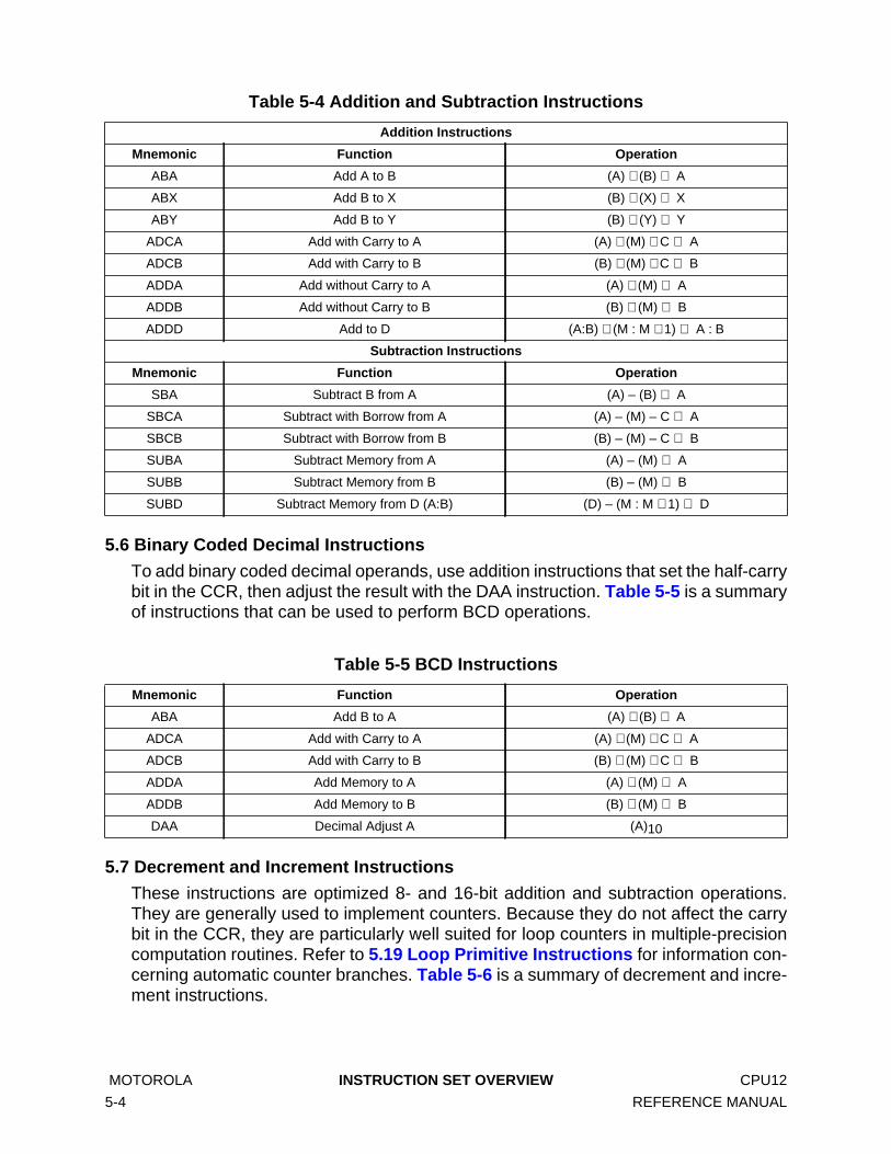
5.6 Binary Coded Decimal Instructions
To add binary coded decimal operands, use addition instructions that set the half-carrybit in the CCR, then adjust the result with the DAA instruction. Table 5-5 is a summaryof instructions that can be used to perform BCD operations.
5.7 Decrement and Increment Instructions
These instructions are optimized 8- and 16-bit addition and subtraction operations.They are generally used to implement counters. Because they do not affect the carrybit in the CCR, they are particularly well suited for loop counters in multiple-precisioncomputation routines. Refer to 5.19 Loop Primitive Instructions for information con-cerning automatic counter branches. Table 5-6 is a summary of decrement and incre-ment instructions.
Table 5-4 Addition and Subtraction Instructions
Addition Instructions
Mnemonic Function Operation
ABA Add A to B (A) + (B) ⇒ A
ABX Add B to X (B) + (X) ⇒ X
ABY Add B to Y (B) + (Y) ⇒ Y
ADCA Add with Carry to A (A) + (M) + C ⇒ A
ADCB Add with Carry to B (B) + (M) + C ⇒ B
ADDA Add without Carry to A (A) + (M) ⇒ A
ADDB Add without Carry to B (B) + (M) ⇒ B
ADDD Add to D (A:B) + (M : M + 1) ⇒ A : B
Subtraction Instructions
Mnemonic Function Operation
SBA Subtract B from A (A) – (B) ⇒ A
SBCA Subtract with Borrow from A (A) – (M) – C ⇒ A
SBCB Subtract with Borrow from B (B) – (M) – C ⇒ B
SUBA Subtract Memory from A (A) – (M) ⇒ A
SUBB Subtract Memory from B (B) – (M) ⇒ B
SUBD Subtract Memory from D (A:B) (D) – (M : M + 1) ⇒ D
Table 5-5 BCD Instructions
Mnemonic Function Operation
ABA Add B to A (A) + (B) ⇒ A
ADCA Add with Carry to A (A) + (M) + C ⇒ A
ADCB Add with Carry to B (B) + (M) + C ⇒ B
ADDA Add Memory to A (A) + (M) ⇒ A
ADDB Add Memory to B (B) + (M) ⇒ B
DAA Decimal Adjust A (A)10
MOTOROLA INSTRUCTION SET OVERVIEW CPU12
5-4 REFERENCE MANUAL

5.8 Compare and Test Instructions
Compare and test instructions perform subtraction between a pair of registers or be-tween a register and memory. The result is not stored, but condition codes are set bythe operation. These instructions are generally used to establish conditions for branchinstructions. In this architecture, most instructions update condition code bits automat-ically, so it is often unnecessary to include separate test or compare instructions. Ta-ble 5-7 is a summary of compare and test instructions.
Table 5-6 Decrement and Increment Instructions
Decrement Instructions
Mnemonic Function Operation
DEC Decrement Memory (M) – $01 ⇒ M
DECA Decrement A (A) – $01 ⇒ A
DECB Decrement B (B) – $01 ⇒ B
DES Decrement SP (SP) – $0001 ⇒ SP
DEX Decrement X (X) – $0001 ⇒ X
DEY Decrement Y (Y) – $0001 ⇒ Y
Increment Instructions
Mnemonic Function Operation
INC Increment Memory (M) + $01 ⇒ M
INCA Increment A (A) + $01 ⇒ A
INCB Increment B (B) + $01 ⇒ B
INS Increment SP (SP) + $0001 ⇒ SP
INX Increment X (X) + $0001 ⇒ X
INY Increment Y (Y) + $0001 ⇒ Y
Table 5-7 Compare and Test Instructions
Compare Instructions
Mnemonic Function Operation
CBA Compare A to B (A) – (B)
CMPA Compare A to Memory (A) – (M)
CMPB Compare B to Memory (B) – (M)
CPD Compare D to Memory (16-bit) (A : B) – (M : M + 1)
CPS Compare SP to Memory (16-bit) (SP) – (M : M + 1)
CPX Compare X to Memory (16-bit) (X) – (M : M + 1)
CPY Compare Y to Memory (16-bit) (Y) – (M : M + 1)
Test Instructions
Mnemonic Function Operation
TST Test Memory for Zero or Minus (M) – $00
TSTA Test A for Zero or Minus (A) – $00
TSTB Test B for Zero or Minus (B) – $00
CPU12 INSTRUCTION SET OVERVIEW MOTOROLA
REFERENCE MANUAL 5-5

5.9 Boolean Logic Instructions
These instructions perform a logic operation between an 8-bit accumulator or the CCRand a memory value. AND, OR, and exclusive OR functions are supported. Table 5-8 summarizes logic instructions.
5.10 Clear, Complement, and Negate Instructions
Each of these instructions performs a specific binary operation on a value in an accu-mulator or in memory. Clear operations clear the value to zero, complement opera-tions replace the value with its one’s complement, and negate operations replace thevalue with its two’s complement. Table 5-9 is a summary of clear, complement andnegate instructions.
Table 5-8 Boolean Logic Instructions
Mnemonic Function Operation
ANDA AND A with Memory (A) • (M) ⇒ A
ANDB AND B with Memory (B) • (M) ⇒ B
ANDCC AND CCR with Memory (Clear CCR Bits) (CCR) • (M) ⇒ CCR
EORA Exclusive OR A with Memory (A) ⊕ (M) ⇒ A
EORB Exclusive OR B with Memory (B) ⊕ (M) ⇒ B
ORAA OR A with Memory (A) + (M) ⇒ A
ORAB OR B with Memory (B) + (M) ⇒ B
ORCC OR CCR with Memory (Set CCR Bits) (CCR) + (M) ⇒ CCR
Table 5-9 Clear, Complement, and Negate Instructions
Mnemonic Function Operation
CLC Clear C Bit in CCR 0 ⇒ C
CLI Clear I Bit in CCR 0 ⇒ I
CLR Clear Memory $00 ⇒ M
CLRA Clear A $00 ⇒ A
CLRB Clear B $00 ⇒ B
CLV Clear V bit in CCR 0 ⇒ V
COM One’s Complement Memory $FF – (M) ⇒ M or (M) ⇒ M
COMA One’s Complement A $FF – (A) ⇒ A or (A) ⇒ A
COMB One’s Complement B $FF – (B) ⇒ B or (B) ⇒ B
NEG Two’s Complement Memory $00 – (M) ⇒ M or (M) + 1 ⇒ M
NEGA Two’s Complement A $00 – (A) ⇒ A or (A) + 1 ⇒ A
NEGB Two’s Complement B $00 – (B) ⇒ B or (B) + 1 ⇒ B
MOTOROLA INSTRUCTION SET OVERVIEW CPU12
5-6 REFERENCE MANUAL
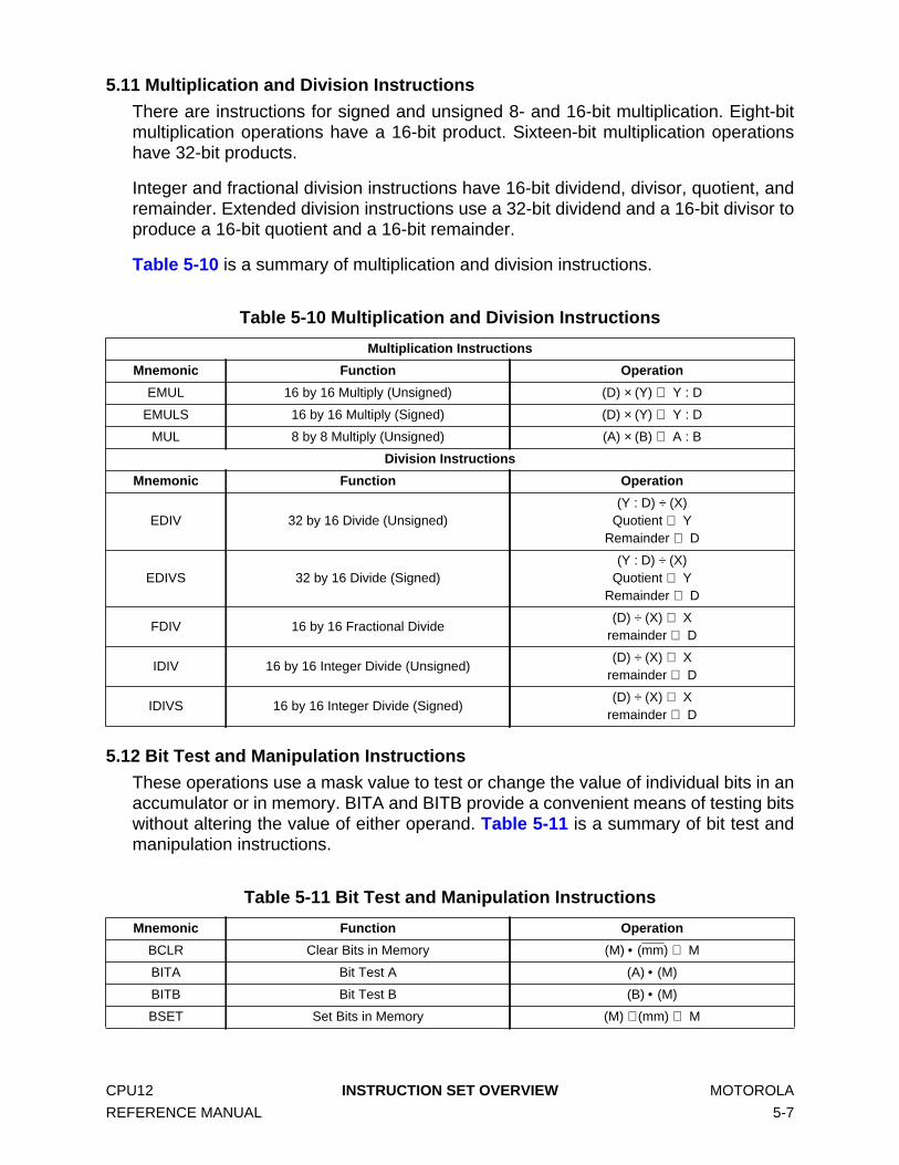
5.11 Multiplication and Division Instructions
There are instructions for signed and unsigned 8- and 16-bit multiplication. Eight-bitmultiplication operations have a 16-bit product. Sixteen-bit multiplication operationshave 32-bit products.
Integer and fractional division instructions have 16-bit dividend, divisor, quotient, andremainder. Extended division instructions use a 32-bit dividend and a 16-bit divisor toproduce a 16-bit quotient and a 16-bit remainder.
Table 5-10 is a summary of multiplication and division instructions.
5.12 Bit Test and Manipulation Instructions
These operations use a mask value to test or change the value of individual bits in anaccumulator or in memory. BITA and BITB provide a convenient means of testing bitswithout altering the value of either operand. Table 5-11 is a summary of bit test andmanipulation instructions.
Table 5-10 Multiplication and Division Instructions
Multiplication Instructions
Mnemonic Function Operation
EMUL 16 by 16 Multiply (Unsigned) (D) × (Y) ⇒ Y : D
EMULS 16 by 16 Multiply (Signed) (D) × (Y) ⇒ Y : D
MUL 8 by 8 Multiply (Unsigned) (A) × (B) ⇒ A : B
Division Instructions
Mnemonic Function Operation
EDIV 32 by 16 Divide (Unsigned)(Y : D) ÷ (X)
Quotient ⇒ YRemainder ⇒ D
EDIVS 32 by 16 Divide (Signed)(Y : D) ÷ (X)
Quotient ⇒ YRemainder ⇒ D
FDIV 16 by 16 Fractional Divide(D) ÷ (X) ⇒ X
remainder ⇒ D
IDIV 16 by 16 Integer Divide (Unsigned)(D) ÷ (X) ⇒ X
remainder ⇒ D
IDIVS 16 by 16 Integer Divide (Signed)(D) ÷ (X) ⇒ X
remainder ⇒ D
Table 5-11 Bit Test and Manipulation Instructions
Mnemonic Function Operation
BCLR Clear Bits in Memory (M) • (mm) ⇒ M
BITA Bit Test A (A) • (M)
BITB Bit Test B (B) • (M)
BSET Set Bits in Memory (M) + (mm) ⇒ M
CPU12 INSTRUCTION SET OVERVIEW MOTOROLA
REFERENCE MANUAL 5-7

5.13 Shift and Rotate Instructions
There are shifts and rotates for all accumulators and for memory bytes. All pass theshifted-out bit through the C status bit to facilitate multiple-byte operations. Becauselogical and arithmetic left shifts are identical, there are no separate logical left shift op-erations. LSL mnemonics are assembled as ASL operations. Table 5-12 shows shiftand rotate instructions.
Table 5-12 Shift and Rotate Instructions
Logical Shifts
Mnemonic Function Operation
LSLLSLALSLB
Logic Shift Left MemoryLogic Shift Left ALogic Shift Left B
LSLD Logic Shift Left D
LSRLSRALSRB
Logic Shift Right MemoryLogic Shift Right ALogic Shift Right B
LSRD Logic Shift Right D
Arithmetic Shifts
Mnemonic Function Operation
ASLASLAASLB
Arithmetic Shift Left MemoryArithmetic Shift Left AArithmetic Shift Left B
ASLD Arithmetic Shift Left D
ASRASRAASRB
Arithmetic Shift Right MemoryArithmetic Shift Right AArithmetic Shift Right B
Rotates
Mnemonic Function Operation
ROLROLAROLB
Rotate Left Memory Through CarryRotate Left A Through CarryRotate Left B Through Carry
RORRORARORB
Rotate Right Memory Through CarryRotate Right A Through CarryRotate Right B Through Carry
C0
b7 b0
C0
b7 b0A Bb7b0
C0
b7 b0
C0
b7 b0A Bb7b0
C0
b7 b0
C0
b7 b0A Bb7b0
Cb7 b0
C b7 b0
Cb7 b0
MOTOROLA INSTRUCTION SET OVERVIEW CPU12
5-8 REFERENCE MANUAL

5.14 Fuzzy Logic Instructions
The CPU12 instruction set includes instructions that support efficient processing offuzzy logic operations. The descriptions of fuzzy logic instructions that follow are func-tional overviews. Table 5-13 summarizes the fuzzy logic instructions. Refer to SEC-TION 9 FUZZY LOGIC SUPPORT for detailed discussion.
5.14.1 Fuzzy Logic Membership Instruction
The MEM instruction is used during the fuzzification process. During fuzzification, cur-rent system input values are compared against stored input membership functions todetermine the degree to which each label of each system input is true. This is accom-plished by finding the y value for the current input on a trapezoidal membership func-tion for each label of each system input. The MEM instruction performs this calculationfor one label of one system input. To perform the complete fuzzification task for a sys-tem, several MEM instructions must be executed, usually in a program loop structure.
5.14.2 Fuzzy Logic Rule Evaluation Instructions
The REV and REVW instructions perform MIN-MAX rule evaluations that are centralelements of a fuzzy logic inference program. Fuzzy input values are processed usinga list of rules from the knowledge base to produce a list of fuzzy outputs. The REV in-struction treats all rules as equally important. The REVW instruction allows each ruleto have a separate weighting factor. The two rule evaluation instructions also differ inthe way rules are encoded into the knowledge base. Because they require a numberof cycles to execute, rule evaluation instructions can be interrupted. Once the interrupthas been serviced, instruction execution resumes at the point the interrupt occurred.
5.14.3 Fuzzy Logic Averaging Instruction
The WAV instruction provides a facility for weighted average calculations. In order tobe usable, the fuzzy outputs produced by rule evaluation must be defuzzified to pro-duce a single output value which represents the combined effect of all of the fuzzy out-puts. Fuzzy outputs correspond to the labels of a system output and each is definedby a membership function in the knowledge base. The CPU12 typically uses single-tons for output membership functions rather than the trapezoidal shapes used for in-puts. As with inputs, the x-axis represents the range of possible values for a systemoutput. Singleton membership functions consist of the x-axis position for a label of thesystem output. Fuzzy outputs correspond to the y-axis height of the correspondingoutput membership function. The WAV instruction calculates the numerator and de-nominator sums for a weighted average of the fuzzy outputs. Because WAV requiresa number of cycles to execute, it can be interrupted. The wavr pseudo-instructioncauses execution to resume at the point it was interrupted.
CPU12 INSTRUCTION SET OVERVIEW MOTOROLA
REFERENCE MANUAL 5-9

Table 5-13 Fuzzy Logic Instructions
Mnemonic Function Operation
MEM Membership Function
µ (grade) ⇒ M(Y)(X) + 4 ⇒ X; (Y) + 1 ⇒ Y; A unchanged
if (A) < P1 or (A) > P2, then µ = 0, elseµ = MIN [((A) – P1) × S1, (P2 – (A)) × S2, $FF]
where:A = current crisp input valueX points to a four byte data structure that describes a trap-
ezoidal membership function as base intercept pointsand slopes (P1, P2, S1, S2)
Y points at fuzzy input (RAM location)
See instruction details for special cases
REV MIN-MAX Rule Evaluation
Find smallest rule input (MIN)Store to rule outputs unless fuzzy output is larger (MAX)
Rules are unweighted
Each rule input is an 8-bit offset from a base address in YEach rule output is an 8-bit offset from a base address in Y$FE separates rule inputs from rule outputs$FF terminates the rule list
REV can be interrupted
REVW MIN-MAX Rule Evaluation
Find smallest rule input (MIN)Multiply by a rule weighting factor (optional)
Store to rule outputs unless fuzzy output is larger (MAX)
Each rule input is the 16-bit address of a fuzzy inputEach rule output is the 16-bit address of a fuzzy outputAddress $FFFE separates rule inputs from rule outputs$FFFF terminates the rule listWeights are 8-bit values in a separate table
REVW can be interrupted
WAV
Calculates Numerator (Sum of Products)and Denominator (Sum of Weights) for
Weighted Average CalculationResults Are Placed in Correct Registers
For EDIV immediately After WAV
wavrResumes Execution of
Interrupted WAV InstructionRecover immediate results from stack
rather than initializing them to zero.
Si F ii 1=
B
∑ Y:D⇒
F ii 1=
B
∑ X⇒
MOTOROLA INSTRUCTION SET OVERVIEW CPU12
5-10 REFERENCE MANUAL

5.15 Maximum and Minimum Instructions
These instructions are used to make comparisons between an accumulator and amemory location. These instructions can be used for linear programming operations,such as Simplex-method optimization or for fuzzification.
MAX and MIN instructions use accumulator A to perform 8-bit comparisons, whileEMAX and EMIN instructions use accumulator D to perform 16-bit comparisons. Theresult (maximum or minimum value) can be stored in the accumulator (EMAXD,EMIND, MAXA, MINA) or the memory address (EMAXM, EMINM, MAXM, MINM).
Table 5-14 is a summary of minimum and maximum instructions.
5.16 Multiply and Accumulate Instruction
The EMACS instruction multiplies two 16-bit operands stored in memory and accumu-lates the 32-bit result in a third memory location. EMACS can be used to implementsimple digital filters and defuzzification routines that use 16-bit operands. The WAVinstruction incorporates an 8- to 16-bit multiply and accumulate operation that obtainsa numerator for the weighted average calculation. The EMACS instruction can auto-mate this portion of the averaging operation when 16-bit operands are used. Table 5-15 shows the EMACS instruction.
Table 5-14 Minimum and Maximum Instructions
Minimum Instructions
Mnemonic Function Operation
EMINDMIN of Two Unsigned 16-Bit Values
Result to AccumulatorMIN ((D), (M : M + 1)) ⇒ D
EMINMMIN of Two Unsigned 16-Bit Values
Result to MemoryMIN ((D), (M : M + 1)) ⇒ M : M+1
MINAMIN of Two Unsigned 8-Bit Values
Result to AccumulatorMIN ((A), (M)) ⇒ A
MINMMIN of Two Unsigned 8-Bit Values
Result to MemoryMIN ((A), (M)) ⇒ M
Maximum Instructions
Mnemonic Function Operation
EMAXDMAX of Two Unsigned 16-Bit Values
Result to AccumulatorMAX ((D), (M : M + 1)) ⇒ D
EMAXMMAX of Two Unsigned 16-Bit Values
Result to MemoryMAX ((D), (M : M + 1)) ⇒ M : M + 1
MAXAMAX of Two Unsigned 8-Bit Values
Result to AccumulatorMAX ((A), (M)) ⇒ A
MAXMMAX of Two Unsigned 8-Bit Values
Result to MemoryMAX((A), (M)) ⇒ M
CPU12 INSTRUCTION SET OVERVIEW MOTOROLA
REFERENCE MANUAL 5-11

5.17 Table Interpolation Instructions
The TBL and ETBL instructions interpolate values from tables stored in memory. Anyfunction that can be represented as a series of linear equations can be represented bya table of appropriate size. Interpolation can be used for many purposes, including tab-ular fuzzy logic membership functions. TBL uses 8-bit table entries and returns an 8-bit result; ETBL uses 16-bit table entries and returns a 16-bit result. Use of indexedaddressing mode provides great flexibility in structuring tables.
Consider each of the successive values stored in a table to be y-values for the end-point of a line segment. The value in the B accumulator before instruction executionbegins represents change in x from the beginning of the line segment to the lookuppoint divided by total change in x from the beginning to the end of the line segment. Bis treated as an 8-bit binary fraction with radix point left of the MSB, so each line seg-ment is effectively divided into 256 smaller segments. During instruction execution, thechange in y between the beginning and end of the segment (a signed byte for TBL ora signed word for ETBL) is multiplied by the content of the B accumulator to obtain anintermediate delta-y term. The result (stored in the A accumulator by TBL, and in theD accumulator by ETBL) is the y-value of the beginning point plus the signed interme-diate delta-y value. Table 5-16 shows the table interpolation instructions.
Table 5-15 Multiply and Accumulate Instructions
Mnemonic Function Operation
EMACSMultiply and Accumulate (Signed)
16 × 16 Bit ⇒ 32 Bit((M(X):M(X+1)) × (M(Y):M(Y+1))) + (M ~ M + 3) ⇒ M ~ M + 3
Table 5-16 Table Interpolation Instructions
Mnemonic Function Operation
ETBL16-Bit Table Lookup and Interpolate
(no indirect addressing modes allowed)
(M : M + 1) + [(B) × ((M + 2 : M + 3) – (M : M + 1))] ⇒ DInitialize B, and index before ETBL.
<ea> points to the first table entry (M : M + 1)B is fractional part of lookup value
TBL8-Bit Table Lookup and Interpolate
(no indirect addressing modes allowed.)
(M) + [(B) × ((M + 1) – (M))] ⇒ AInitialize B, and index before TBL.
<ea> points to the first 8-bit table entry (M)B is fractional part of lookup value.
MOTOROLA INSTRUCTION SET OVERVIEW CPU12
5-12 REFERENCE MANUAL

5.18 Branch Instructions
Branch instructions cause sequence to change when specific conditions exist. TheCPU12 uses three kinds of branch instructions. These are short branches, longbranches, and bit-conditional branches.
Branch instructions can also be classified by the type of condition that must be satis-fied in order for a branch to be taken. Some instructions belong to more than one clas-sification.
Unary branch instructions always execute.
Simple branches are taken when a specific bit in the condition code register is in aspecific state as a result of a previous operation.
Unsigned branches are taken when comparison or test of unsigned quantities re-sults in a specific combination of condition code register bits.
Signed branches are taken when comparison or test of signed quantities results ina specific combination of condition code register bits.
5.18.1 Short Branch Instructions
Short branch instructions operate as follows. When a specified condition is met, asigned 8-bit offset is added to the value in the program counter. Program executioncontinues at the new address.
The numeric range of short branch offset values is $80 (–128) to $7F (127) from theaddress of the next memory location after the offset value.
Table 5-17 is a summary of the short branch instructions.
5.18.2 Long Branch Instructions
Long branch instructions operate as follows. When a specified condition is met, asigned 16-bit offset is added to the value in the program counter. Program executioncontinues at the new address. Long branches are used when large displacements be-tween decision-making steps are necessary.
The numeric range of long branch offset values is $8000 (–32,768) to $7FFF (32,767)from the address of the next memory location after the offset value. This permitsbranching from any location in the standard 64-Kbyte address map to any other loca-tion in the map.
Table 5-18 is a summary of the long branch instructions.
CPU12 INSTRUCTION SET OVERVIEW MOTOROLA
REFERENCE MANUAL 5-13

Table 5-17 Short Branch Instructions
Unary Branches
Mnemonic Function Equation or Operation
BRA Branch Always 1 = 1
BRN Branch Never 1 = 0
Simple Branches
Mnemonic Function Equation or Operation
BCC Branch if Carry Clear C = 0
BCS Branch if Carry Set C = 1
BEQ Branch if Equal Z = 1
BMI Branch if Minus N = 1
BNE Branch if Not Equal Z = 0
BPL Branch if Plus N = 0
BVC Branch if Overflow Clear V = 0
BVS Branch if Overflow Set V = 1
Unsigned Branches
Mnemonic Function Relation Equation or Operation
BHI Branch if Higher R > M C + Z = 0
BHS Branch if Higher or Same R ≥ M C = 0
BLO Branch if Lower R < M C = 1
BLS Branch if Lower or Same R ≤ M C + Z = 1
Signed Branches
Mnemonic Function Relation Equation or Operation
BGE Branch if Greater Than or Equal R ≥ M N ⊕ V = 0
BGT Branch if Greater Than R > M Z + (N ⊕ V) = 0
BLE Branch if Less Than or Equal R ≤ M Z + (N ⊕ V) = 1
BLT Branch if Less Than R < M N ⊕ V = 1
MOTOROLA INSTRUCTION SET OVERVIEW CPU12
5-14 REFERENCE MANUAL

Table 5-18 Long Branch Instructions
Unary Branches
Mnemonic Function Equation or Operation
LBRA Long Branch Always 1 = 1
LBRN Long Branch Never 1 = 0
Simple Branches
Mnemonic Function Equation or Operation
LBCC Long Branch if Carry Clear C = 0
LBCS Long Branch if Carry Set C = 1
LBEQ Long Branch if Equal Z = 1
LBMI Long Branch if Minus N = 1
LBNE Long Branch if Not Equal Z = 0
LBPL Long Branch if Plus N = 0
LBVC Long Branch if Overflow Clear V = 0
LBVS Long Branch if Overflow Set V = 1
Unsigned Branches
Mnemonic Function Equation or Operation
LBHI Long Branch if Higher C + Z = 0
LBHS Long Branch if Higher or Same C = 0
LBLO Long Branch if Lower Z = 1
LBLS Long Branch if Lower or Same C + Z = 1
Signed Branches
Mnemonic Function Equation or Operation
LBGE Long Branch if Greater Than or Equal N ⊕ V = 0
LBGT Long Branch if Greater Than Z + (N ⊕ V) = 0
LBLE Long Branch if Less Than or Equal Z + (N ⊕ V) = 1
LBLT Long Branch if Less Than N ⊕ V = 1
CPU12 INSTRUCTION SET OVERVIEW MOTOROLA
REFERENCE MANUAL 5-15

5.18.3 Bit Condition Branch Instructions
These branches are taken when bits in a memory byte are in a specific state. A maskoperand is used to test the location. If all bits in that location that correspond to onesin the mask are set (BRSET) or cleared (BRCLR), the branch is taken.
The numeric range of 8-bit offset values is $80 (–128) to $7F (127) from the addressof the next memory location after the offset value. Table 5-19 is a summary of bit-con-dition branches.
5.19 Loop Primitive Instructions
The loop primitives can also be thought of as counter branches. The instructions testa counter value in a register or accumulator (A, B, D, X, Y, or SP) for zero or nonzerovalue as a branch condition. There are predecrement, preincrement and test-only ver-sions of these instructions.
The numeric range of 8-bit offset values is $80 (–128) to $7F (127) from the addressof the next memory location after the offset value. Table 5-20 is a summary of loopprimitive branches.
Table 5-19 Bit Condition Branch Instructions
Mnemonic Function Equation or Operation
BRCLR Branch if Selected Bits Clear (M) • (mm) = 0
BRSET Branch if Selected Bits Set (M) • (mm) = 0
Table 5-20 Loop Primitive Instructions
Mnemonic Function Equation or Operation
DBEQDecrement counter and branch if = 0
(counter = A, B, D, X, Y, or SP)
(counter) – 1⇒ counterIf (counter) = 0, then branch
else continue to next instruction
DBNEDecrement counter and branch if ≠ 0
(counter = A, B, D, X, Y, or SP)
(counter) – 1⇒ counterIf (counter) not = 0, then branchelse continue to next instruction
IBEQIncrement counter and branch if = 0
(counter = A, B, D, X, Y, or SP)
(counter) + 1⇒ counterIf (counter) = 0, then branch
else continue to next instruction
IBNEIncrement counter and branch if ≠ 0
(counter = A, B, D, X, Y, or SP)
(counter) + 1⇒ counterIf (counter) not = 0, then branchelse continue to next instruction
TBEQTest counter and branch if = 0(counter = A, B, D, X,Y, or SP)
If (counter) = 0, then branchelse continue to next instruction
TBNETest counter and branch if ≠ 0(counter = A, B, D, X,Y, or SP)
If (counter) not = 0, then branchelse continue to next instruction
MOTOROLA INSTRUCTION SET OVERVIEW CPU12
5-16 REFERENCE MANUAL

5.20 Jump and Subroutine Instructions
Jump instructions cause immediate changes in sequence. The JMP instruction loadsthe PC with an address in the 64-Kbyte memory map, and program execution contin-ues at that address. The address can be provided as an absolute 16-bit address ordetermined by various forms of indexed addressing.
Subroutine instructions optimize the process of transferring control to a code segmentthat performs a particular task. A short branch (BSR), a jump (JSR), or an expanded-memory call (CALL) can be used to initiate subroutines. There is no LBSR instruction,but a PC-relative JSR performs the same function. A return address is stacked, thenexecution begins at the subroutine address. Subroutines in the normal 64-Kbyte ad-dress space are terminated with an RTS instruction. RTS unstacks the return addressso that execution resumes with the instruction after BSR or JSR.
The CALL instruction is intended for use with expanded memory. CALL stacks the val-ue in the PPAGE register and the return address, then writes a new value to PPAGEto select the memory page where the subroutine resides. The page value is an imme-diate operand in all addressing modes except indexed indirect modes; in these modes,an operand points to locations in memory where the new page value and subroutineaddress are stored. The RTC instruction is used to terminate subroutines in expandedmemory. RTC unstacks the PPAGE value and the return address so that executionresumes with the next instruction after CALL. For software compatibility, CALL andRTC execute correctly on devices that do not have expanded addressing capability.Table 5-21 summarizes the jump and subroutine instructions.
Table 5-21 Jump and Subroutine Instructions
Mnemonic Function Operation
BSR Branch to SubroutineSP – 2 ⇒ SP
RTNH : RTNL ⇒ M(SP) : M(SP+1)Subroutine address ⇒ PC
CALL Call Subroutine in Expanded Memory
SP – 2 ⇒ SPRTNH:RTNL⇒ M(SP) : M(SP+1)
SP – 1 ⇒ SP(PPAGE) ⇒ M(SP)Page ⇒ PPAGE
Subroutine address ⇒ PC
JMP Jump Subroutine Address ⇒ PC
JSR Jump to SubroutineSP – 2 ⇒ SP
RTNH : RTNL⇒ M(SP) : M(SP+1)Subroutine address ⇒ PC
RTC Return from CallM(SP) : M(SP+1) ⇒ PCH : PCL
SP + 2 ⇒ SP
RTS Return from Subroutine
M(SP) ⇒ PPAGESP + 1 ⇒ SP
M(SP) : M(SP+1) ⇒ PCH : PCLSP + 2 ⇒ SP
CPU12 INSTRUCTION SET OVERVIEW MOTOROLA
REFERENCE MANUAL 5-17

5.21 Interrupt Instructions
Interrupt instructions handle transfer of control to a routine that performs a critical task.Software interrupts are a type of exception. SECTION 7 EXCEPTION PROCESSINGcovers interrupt exception processing in detail.
The SWI instruction initiates synchronous exception processing. First, the return PCvalue is stacked. After CPU context is stacked, execution continues at the addresspointed to by the SWI vector.
Execution of the SWI instruction causes an interrupt without an interrupt service re-quest. SWI is not inhibited by global mask bits I and X in the CCR, and execution ofSWI sets the I mask bit. Once an SWI interrupt begins, maskable interrupts are inhib-ited until the I bit in the CCR is cleared. This typically occurs when an RTI instructionat the end of the SWI service routine restores context.
The CPU12 uses the software interrupt for unimplemented opcode trapping. There areopcodes in all 256 positions in the page 1 opcode map, but only 54 of the 256 positionson page 2 of the opcode map are used. If the CPU attempts to execute one of the un-implemented opcodes on page 2, an opcode trap interrupt occurs. Traps are essen-tially interrupts that share the $FFF8:$FFF9 interrupt vector.
The RTI instruction is used to terminate all exception handlers, including interrupt ser-vice routines. RTI first restores the CCR, B:A, X, Y, and the return address from thestack. If no other interrupt is pending, normal execution resumes with the instructionfollowing the last instruction that executed prior to interrupt.
Table 5-22 is a summary of interrupt instructions.
Table 5-22 Interrupt InstructionsMnemonic Function Operation
RTI Return from Interrupt
(M(SP)) ⇒ CCR; (SP) + $0001 ⇒ SP(M(SP) : M(SP+1)) ⇒ B : A; (SP) + $0002 ⇒ SP
(M(SP) : M(SP+1)) ⇒ XH : XL; (SP) + $0004 ⇒ SP(M(SP) : M(SP+1)) ⇒ PCH : PCL; (SP) + $0002 ⇒ SP
(M(SP) : M(SP+1)) ⇒ YH : YL; (SP) + $0004 ⇒ SP
SWI Software Interrupt
SP – 2 ⇒ SP; RTNH : RTNL ⇒ M(SP) : M(SP+1)
SP – 2 ⇒ SP; YH : YL ⇒ M(SP) : M(SP+1)
SP – 2 ⇒ SP; XH : XL ⇒ M(SP) : M(SP+1)
SP – 2 ⇒ SP; B : A ⇒ M(SP) : M(SP+1)
SP – 1 ⇒ SP; CCR ⇒ M(SP)
TRAP Software Interrupt
SP – 2 ⇒ SP; RTNH : RTNL ⇒ M(SP) : M(SP+1)
SP – 2 ⇒ SP; YH : YL ⇒ M(SP) : M(SP+1)
SP – 2 ⇒ SP; XH : XL ⇒ M(SP) : M(SP+1)
SP – 2 ⇒ SP; B : A ⇒ M(SP) : M(SP+1)
SP – 1 ⇒ SP; CCR ⇒ M(SP)
MOTOROLA INSTRUCTION SET OVERVIEW CPU12
5-18 REFERENCE MANUAL

5.22 Index Manipulation Instructions
These instructions perform 8- and 16-bit operations on the three index registers andaccumulators, other registers, or memory, as shown in Table 5-23 .
Table 5-23 Index Manipulation Instructions
Addition Instructions
Mnemonic Function Operation
ABX Add B to X (B) + (X) ⇒ X
ABY Add B to Y (B) + (Y) ⇒ Y
Compare Instructions
Mnemonic Function Operation
CPS Compare SP to Memory (SP) – (M : M + 1)
CPX Compare X to Memory (X) – (M : M + 1)
CPY Compare Y to Memory (Y) – (M : M + 1)
Load Instructions
Mnemonic Function Operation
LDS Load SP from Memory M : M+1 ⇒ SP
LDX Load X from Memory (M : M + 1) ⇒ X
LDY Load Y from Memory (M : M + 1) ⇒ Y
LEAS Load Effective Address into SP Effective Address ⇒ SP
LEAX Load Effective Address into X Effective Address ⇒ X
LEAY Load Effective Address into Y Effective Address ⇒ Y
Store Instructions
Mnemonic Function Operation
STS Store SP in Memory (SP) ⇒ M:M+1
STX Store X in Memory (X) ⇒ M : M + 1
STY Store Y in Memory (Y) ⇒ M : M + 1
Transfer Instructions
Mnemonic Function Operation
TFR Transfer Register to Register (A, B, CCR, D, X, Y, or SP) ⇒ A, B, CCR, D, X, Y, or SP
TSX Transfer SP to X (SP) ⇒ X
TSY Transfer SP to Y (SP) ⇒ Y
TXS Transfer X to SP (X) ⇒ SP
TYS Transfer Y to SP (Y) ⇒ SP
Exchange Instructions
Mnemonic Function Operation
EXG Exchange Register to Register (A, B, CCR, D, X, Y, or SP) ⇔ (A, B, CCR, D, X, Y, or SP)
XGDX EXchange D with X (D) ⇔ (X)
XGDY EXchange D with Y (D) ⇔ (Y)
CPU12 INSTRUCTION SET OVERVIEW MOTOROLA
REFERENCE MANUAL 5-19

5.23 Stacking Instructions
There are two types of stacking instructions, as shown in Table 5-24 . Stack pointerinstructions use specialized forms of mathematical and data transfer instructions toperform stack pointer manipulation. Stack operation instructions save information onand retrieve information from the system stack.
5.24 Pointer and Index Calculation Instructions
The load effective address instructions allow 5-, 8-, or 16-bit constants, or the contentsof 8-bit accumulators A and B or 16-bit accumulator D to be added to the contents ofthe X and Y index registers, the SP, or the PC. Table 5-25 is a summary of pointer andindex instructions.
Table 5-24 Stacking Instructions
Stack Pointer Instructions
Mnemonic Function Operation
CPS Compare SP to Memory (SP) – (M : M + 1)
DES Decrement SP (SP) – 1 ⇒ SP
INS Increment SP (SP) + 1 ⇒ SP
LDS Load SP (M : M + 1) ⇒ SP
LEAS Load Effective Address into SP Effective Address ⇒ SP
STS Store SP (SP) ⇒ M : M + 1
TSX Transfer SP to X (SP) ⇒ X
TSY Transfer SP to Y (SP) ⇒ Y
TXS Transfer X to SP (X) ⇒ SP
TYS Transfer Y to SP (Y) ⇒ SP
Stack Operation Instructions
Mnemonic Function Operation
PSHA Push A (SP) – 1 ⇒ SP; (A) ⇒ M(SP)
PSHB Push B (SP) – 1 ⇒ SP; (B) ⇒ M(SP)
PSHC Push CCR (SP) – 1 ⇒ SP; (A) ⇒ M(SP)
PSHD Push D (SP) – 2 ⇒ SP; (A : B) ⇒ M(SP) : M(SP+1)
PSHX Push X (SP) – 2 ⇒ SP; (X) ⇒ M(SP) : M(SP+1)
PSHY Push Y (SP) – 2 ⇒ SP; (Y) ⇒ M(SP) : M(SP+1)
PULA Pull A (M(SP)) ⇒ A; (SP) + 1 ⇒ SP
PULB Pull B (M(SP)) ⇒ B; (SP) + 1 ⇒ SP
PULC Pull CCR (M(SP)) ⇒ CCR; (SP) + 1 ⇒ SP
PULD Pull D (M(SP) : M(SP+1)) ⇒ A : B; (SP) + 2 ⇒ SP
PULX Pull X (M(SP) : M(SP+1)) ⇒ X; (SP) + 2 ⇒ SP
PULY Pull Y (M(SP) : M(SP+1)) ⇒ Y; (SP) + 2 ⇒ SP
MOTOROLA INSTRUCTION SET OVERVIEW CPU12
5-20 REFERENCE MANUAL

5.25 Condition Code Instructions
Condition code instructions are special forms of mathematical and data transfer in-structions that can be used to change the condition code register. Table 5-26 showsinstructions that can be used to manipulate the CCR.
5.26 Stop and Wait Instructions
As shown in Table 5-27 , there are two instructions that put the CPU12 in an inactivestate that reduces power consumption.
The stop instruction (STOP) stacks a return address and the contents of CPU registersand accumulators, then halts all system clocks.
The wait instruction (WAI) stacks a return address and the contents of CPU registersand accumulators, then waits for an interrupt service request; however, system clocksignals continue to run.
Table 5-25 Pointer and Index Calculation Instructions
Mnemonic Function Operation
LEASLoad Result of Indexed Addressing Mode
Effective Address Calculationinto Stack Pointer
r ± Constant ⇒ SP or(r) + (Accumulator) ⇒ SP
r = X, Y, SP, or PC
LEAXLoad Result of Indexed Addressing Mode
Effective Address Calculationinto X Index Register
r ± Constant ⇒X or(r) + (Accumulator) ⇒X
r = X, Y, SP, or PC
LEAYLoad Result of Indexed Addressing Mode
Effective Address Calculationinto Y Index Register
r ± Constant ⇒Y or(r) + (Accumulator) ⇒ Y
r = X, Y, SP, or PC
Table 5-26 Condition Codes Instructions
Mnemonic Function Operation
ANDCC Logical AND CCR with Memory (CCR) • (M) ⇒ CCR
CLC Clear C Bit 0 ⇒ C
CLI Clear I Bit 0 ⇒ I
CLV Clear V Bit 0 ⇒ V
ORCC Logical OR CCR with Memory (CCR) + (M) ⇒ CCR
PSHC Push CCR onto Stack (SP) – 1 ⇒ SP; (CCR) ⇒ M(SP)
PULC Pull CCR from Stack (M(SP)) ⇒ CCR; (SP) + 1 ⇒ SP
SEC Set C Bit 1 ⇒ C
SEI Set I Bit 1 ⇒ I
SEV Set V Bit 1 ⇒ V
TAP Transfer A to CCR (A) ⇒ CCR
TPA Transfer CCR to A (CCR) ⇒ A
CPU12 INSTRUCTION SET OVERVIEW MOTOROLA
REFERENCE MANUAL 5-21

Both STOP and WAI require that either an interrupt or a reset exception occur beforenormal execution of instructions resumes. Although both instructions require the samenumber of clock cycles to resume normal program execution after an interrupt servicerequest is made, restarting after a STOP requires extra time for the oscillator to reachoperating speed.
5.27 Background Mode and Null Operations
Background debug mode is a special CPU12 operating mode that is used for systemdevelopment and debugging. Executing BGND when BDM is enabled puts the CPU12in this mode. For complete information refer to SECTION 8 DEVELOPMENT ANDDEBUG SUPPORT.
Null operations are often used to replace other instructions during software debugging.Replacing conditional branch instructions with BRN, for instance, permits testing a de-cision-making routine without actually taking the branches.
Table 5-28 shows the BGND and NOP instructions.
Table 5-27 Stop and Wait Instructions
Mnemonic Function Operation
STOP Stop
SP – 2 ⇒ SP; RTNH : RTNL ⇒ M(SP) : M(SP+1)
SP – 2 ⇒ SP; YH : YL ⇒ M(SP) : M(SP+1)
SP – 2 ⇒ SP; XH : XL ⇒ M(SP) : M(SP+1)
SP – 2 ⇒ SP; B : A ⇒ M(SP) : M(SP+1)
SP – 1 ⇒ SP; CCR ⇒ M(SP)
STOP CPU Clocks
WAI Wait for Interrupt
SP – 2 ⇒ SP; RTNH : RTNL ⇒ M(SP) : M(SP+1)
SP – 2 ⇒ SP; YH : YL ⇒ M(SP) : M(SP+1)
SP – 2 ⇒ SP; XH : XL ⇒ M(SP) : M(SP+1)
SP – 2 ⇒ SP; B : A ⇒ M(SP) : M(SP+1)
SP – 1 ⇒ SP; CCR ⇒ M(SP)
Table 5-28 Background Mode and Null Operation Instructions
Mnemonic Function Operation
BGND Enter Background Debug ModeIf BDM enabled, enter BDM;
else, resume normal processing
BRN Branch Never Does not branch
LBRN Long Branch Never Does not branch
NOP Null operation —
MOTOROLA INSTRUCTION SET OVERVIEW CPU12
5-22 REFERENCE MANUAL

SECTION 6INSTRUCTION GLOSSARY
This section is a comprehensive reference to the CPU12 instruction set.
6.1 Glossary Information
The glossary contains an entry for each assembler mnemonic, in alphabetic order.Figure 6-1 is a representation of a glossary page.
Figure 6-1 Example Glossary Page
Source Form Address Mode
S X H
— — ∆
N: Set if MSB of resu
Z: Set if result is $00
V: 0; Cleared.
Addressing Modes, Machine Code, an
Load Inde
Operation: (M : M + 1) ⇒
Description: Loads the most significamemory at the addres
Condition Codes and Boolean Form
LDX
Obje
X
LDXLDXLDXLDXLDXLDXLDXLDX
#opr16iopr8aopr16aoprx0_xyspoprx9,xyspoprx16,xysp[D,xysp][oprx16,xysp]
IMMDIREXTIDXIDX1IDX2
[D,IDX][IDX2]
CE jjDE dFE hEEEE
EX GLO PG
DETAILED SYNTAXAND
CYCLE-BY-CYCLEOPERATION
EFFECT ONCONDITION CODE REGISTER
STATUS BITS
DETAILED DESCRIPTIONOF OPERATION
SYMBOLIC DESCRIPTIONOF OPERATION
MNEMONIC
CPU12 INSTRUCTION GLOSSARY MOTOROLA
REFERENCE MANUAL 6-1

Each entry contains symbolic and textual descriptions of operation, information con-cerning the effect of operation on status bits in the condition code register, and a tablethat describes assembler syntax, cycle count, and cycle-by-cycle execution of the in-struction.
6.2 Condition Code Changes
The following special characters are used to describe the effects of instruction execu-tion on the status bits in the condition codes register.
6.3 Object Code Notation
The digits 0 to 9 and the upper case letters A to F are used to express hexadecimalvalues. Pairs of lower case letters represent the 8-bit values as described below.
– — Status bit not affected by operation.
0 — Status bit cleared by operation.
1 — Status bit set by operation.
∆ — Status bit affected by operation.
⇓ — Status bit may be cleared or remain set, but is not set by operation.
⇑ — Status bit may be set or remain cleared, but is not cleared by operation.
? — Status bit may be changed by operation but the final state is not defined.
! — Status bit used for a special purpose.
dd — 8-bit direct address $0000 to $00FF. (High byte assumed to be $00).
ee — High-order byte of a 16-bit constant offset for indexed addressing.
eb — Exchange/Transfer post-byte.
ff — Low-order eight bits of a 9-bit signed constant offset for indexed addressing, orlow-order byte of a 16-bit constant offset for indexed addressing.
hh — High-order byte of a 16-bit extended address.
ii — 8-bit immediate data value.
jj — High-order byte of a 16-bit immediate data value.
kk — Low-order byte of a 16-bit immediate data value.
lb — Loop primitive (DBNE) post-byte.
ll — Low-order byte of a 16-bit extended address.
mm — 8-bit immediate mask value for bit manipulation instructions.Set bits indicate bits to be affected.
pg — Program overlay page (bank) number used in CALL instruction.
qq — High-order byte of a 16-bit relative offset for long branches.
tn — Trap number $30–$39 or $40–$FF.
rr — Signed relative offset $80 (–128) to $7F (+127).Offset relative to the byte following the relative offset byte, orlow-order byte of a 16-bit relative offset for long branches.
xb — Indexed addressing post-byte.
MOTOROLA INSTRUCTION GLOSSARY CPU12
6-2 REFERENCE MANUAL

6.4 Source Forms
The glossary pages provide only essential information about assembler source forms.Assemblers generally support a number of assembler directives, allow definition ofprogram labels, and have special conventions for comments. For complete informa-tion about writing source files for a particular assembler, refer to the documentationprovided by the assembler vendor.
Assemblers are typically very flexible about the use of spaces and tabs. Often, anynumber of spaces or tabs can be used where a single space is shown on the glossarypages. Spaces and tabs are also normally allowed before and after commas. Whenprogram labels are used, there must also be at least one tab or space before all in-struction mnemonics. This required space is not apparent in the source forms.
Everything in the source forms columns, except expressions in italic characters, is lit-eral information which must appear in the assembly source file exactly as shown. Theinitial 3- to 5-letter mnemonic is always a literal expression. All commas, pound signs(#), parentheses, square brackets ( [ or ] ), plus signs (+), minus signs (–), and the reg-ister designation D (as in [D,... ), are literal characters.
Groups of italic characters in the columns represent variable information to be sup-plied by the programmer. These groups can include any alphanumeric character or theunderscore character, but cannot include a space or comma. For example, the groupsxysp and oprx0_xysp are both valid, but the two groups oprx0 xysp are not valid be-cause there is a space between them. Permitted syntax is described below.
The definition of a legal label or expression varies from assembler to assembler. As-semblers also vary in the way CPU registers are specified. Refer to assembler docu-mentation for detailed information. Recommended register designators are a, A, b, B,ccr, CCR, d, D, x, X, y, Y, sp, SP, pc, and PC.
abc — Any one legal register designator for accumulators A or B or the CCR.
abcdxys — Any one legal register designator for accumulators A or B, the CCR, the doubleaccumulator D, index registers X or Y, or the SP. Some assemblers may acceptt2, T2, t3, or T3 codes in certain cases of transfer and exchange instructions, butthese forms are intended for Motorola use only.
abd — Any one legal register designator for accumulators A or B or the double accumu-lator D.
abdxys — Any one legal register designator for accumulators A or B, the double accumulatorD, index register X or Y, or the SP.
dxys — Any one legal register designation for the double accumulator D, index registers Xor Y, or the SP.
msk8 — Any label or expression that evaluates to an 8-bit value. Some assemblers requirea # symbol before this value.
opr8i — Any label or expression that evaluates to an 8-bit immediate value.
opr16i — Any label or expression that evaluates to a 16-bit immediate value.
opr8a — Any label or expression that evaluates to an 8-bit value. The instruction treats this8-bit value as the low order 8-bits of an address in the direct page of the 64-Kbyteaddress space ($00xx).
CPU12 INSTRUCTION GLOSSARY MOTOROLA
REFERENCE MANUAL 6-3

opr16a — Any label or expression that evaluates to a 16-bit value. The instruction treats thisvalue as an address in the 64-Kbyte address space.
oprx0_xysp — This word breaks down into one of the following alternative forms that assembleto an 8-bit indexed addressing postbyte code. These forms generate the same ob-ject code except for the value of the postbyte code, which is designated as xb inthe object code columns of the glossary pages. As with the source forms, treat allcommas, plus signs, and minus signs as literal syntax elements. The italicizedwords used in these forms are included in this key.oprx5,xyspoprx3,–xysoprx3,+xysoprx3,xys–oprx3,xys+abd,xysp
oprx3 — Any label or expression that evaluates to a value in the range +1 to +8.
oprx5 — Any label or expression that evaluates to a 5-bit value in the range –16 to +15.
oprx9 — Any label or expression that evaluates to a 9-bit value in the range –256 to +255.
oprx16 — Any label or expression that evaluates to a 16-bit value. Since the CPU12 has a16-bit address bus, this can be either a signed or an unsigned value.
page — Any label or expression that evaluates to an 8-bit value. The CPU12 recognizesup to an 8-bit page value for memory expansion but not all MCUs that include theCPU12 implement all of these bits. It is the programmer’s responsibility to limit thepage value to legal values for the intended MCU system. Some assemblers re-quire a # symbol before this value.
rel8 — Any label or expression that refers to an address that is within –256 to +255 loca-tions from the next address after the last byte of object code for the current instruc-tion. The assembler will calculate the 8-bit signed offset and include it in the objectcode for this instruction.
rel9 — Any label or expression that refers to an address that is within –512 to +511 loca-tions from the next address after the last byte of object code for the current instruc-tion. The assembler will calculate the 9-bit signed offset and include it in the objectcode for this instruction. The sign bit for this 9-bit value is encoded by the assem-bler as a bit in the looping postbyte (lb) of one of the loop control instructionsDBEQ, DBNE, IBEQ, IBNE, TBEQ, or TBNE. The remaining eight bits of the offsetare included as an extra byte of object code.
rel16 — Any label or expression that refers to an address anywhere in the 64-Kbyte ad-dress space. The assembler will calculate the 16-bit signed offset between this ad-dress and the next address after the last byte of object code for this instruction,and include it in the object code for this instruction.
trapnum — Any label or expression that evaluates to an 8-bit number in the range $30–$39 or$40–$FF. Used for TRAP instruction.
xys — Any one legal register designation for index registers X or Y or the SP.
xysp — Any one legal register designation for index registers X or Y, the SP, or the PC.The reference point for PC relative instructions is the next address after the lastbyte of object code for the current instruction.
MOTOROLA INSTRUCTION GLOSSARY CPU12
6-4 REFERENCE MANUAL

6.5 Cycle-by-Cycle Execution
This information is found in the tables at the bottom of each instruction glossary page.Entries show how many bytes of information are accessed from different areas ofmemory during the course of instruction execution. With this information and knowl-edge of the type and speed of memory in the system, a user can determine the exe-cution time for any instruction in any system.
A single letter code in the column represents a single CPU cycle. Upper case lettersindicate 16-bit access cycles. There are cycle codes for each addressing mode varia-tion of each instruction. Simply count code letters to determine the execution time ofan instruction in a best-case system. An example of a best-case system is a single-chip 16-bit system with no 16-bit off-boundary data accesses to any locations otherthan on-chip RAM.
Many conditions can cause one or more instruction cycles to be stretched, but theCPU is not aware of the stretch delays because the clock to the CPU is temporarilystopped during these delays.
The following paragraphs explain the cycle code letters used and note conditions thatcan cause each type of cycle to be stretched.
f — Free cycle. This indicates a cycle where the CPU does not require use of thesystem buses. An f cycle is always one cycle of the system bus clock. Thesecycles can be used by a queue controller or the background debug system toperform single cycle accesses without disturbing the CPU.
g — Read 8-bit PPAGE register. These cycles are only used with the CALL instruc-tion to read the current value of the PPAGE register, and are not visible on theexternal bus. Since the PPAGE register is an internal 8-bit register, these cyclesare never stretched.
I — Read indirect pointer. Indexed indirect instructions use this 16-bit pointer frommemory to address the operand for the instruction. These are always 16-bitreads but they can be either aligned or misaligned. These cycles are extendedto two bus cycles if the MCU is operating with an 8-bit external data bus and thecorresponding data is stored in external memory. There can be additionalstretching when the address space is assigned to a chip-select circuit pro-grammed for slow memory. These cycles are also stretched if they correspondto misaligned access to a memory that is not designed for single-cycle mis-aligned access.
i — Read indirect PPAGE value. These cycles are only used with indexed indirectversions of the CALL instruction, where the 8-bit value for the memory expan-sion page register of the CALL destination is fetched from an indirect memorylocation. These cycles are stretched only when controlled by a chip-select circuitthat is programmed for slow memory.
n — Write 8-bit PPAGE register. These cycles are only used with the CALL and RTCinstructions to write the destination value of the PPAGE register and are not vis-ible on the external bus. Since the PPAGE register is an internal 8-bit register,these cycles are never stretched.
CPU12 INSTRUCTION GLOSSARY MOTOROLA
REFERENCE MANUAL 6-5

O — Optional cycle. Program information is always fetched as aligned 16-bit words.When an instruction consists of an odd number of bytes, and the first byte is mis-aligned, an O cycle is used to make an additional program word access (P) cyclethat maintains queue order. In all other cases, the O cycle appears as a free (f)cycle. The $18 prebyte for page two opcodes is treated as a special one-byteinstruction. If the prebyte is misaligned, the O cycle is used as a program wordaccess for the prebyte; if the prebyte is aligned, the O cycle appears as a freecycle. If the remainder of the instruction consists of an odd number of bytes, an-other O cycle is required some time before the instruction is completed. If the Ocycle for the prebyte is treated as a P cycle, any subsequent O cycle in the sameinstruction is treated as an f cycle; if the O cycle for the prebyte is treated as anf cycle, any subsequent O cycle in the same instruction is treated as a P cycle.Optional cycles used for program word accesses can be extended to two buscycles if the MCU is operating with an 8-bit external data bus and the programis stored in external memory. There can be additional stretching when the ad-dress space is assigned to a chip-select circuit programmed for slow memory.Optional cycles used as free cycles are never stretched.
P — Program word access. Program information is fetched as aligned 16-bit words.These cycles are extended to two bus cycles if the MCU is operating with an 8-bit external data bus and the program is stored externally. There can be addi-tional stretching when the address space is assigned to a chip-select circuit pro-grammed for slow memory.
r — 8-bit data read. These cycles are stretched only when controlled by a chip-selectcircuit programmed for slow memory.
R — 16-bit data read. These cycles are extended to two bus cycles if the MCU is op-erating with an 8-bit external data bus and the corresponding data is stored inexternal memory. There can be additional stretching when the address space isassigned to a chip-select circuit programmed for slow memory. These cyclesare also stretched if they correspond to misaligned accesses to memory that isnot designed for single-cycle misaligned access.
s — Stack 8-bit data. These cycles are stretched only when controlled by a chip-se-lect circuit programmed for slow memory.
S — Stack 16-bit data. These cycles are extended to two bus cycles if the MCU isoperating with an 8-bit external data bus and the SP is pointing to external mem-ory. There can be additional stretching if the address space is assigned to achip-select circuit programmed for slow memory. These cycles are alsostretched if they correspond to misaligned accesses to a memory that is not de-signed for single cycle misaligned access. The internal RAM is designed to al-low single cycle misaligned word access.
w — 8-bit data write. These cycles are stretched only when controlled by a chip-se-lect circuit programmed for slow memory.
W — 16-bit data write. These cycles are extended to two bus cycles if the MCU is op-erating with an 8-bit external data bus and the corresponding data is stored inexternal memory. There can be additional stretching when the address space isassigned to a chip-select circuit programmed for slow memory. These cyclesare also stretched if they correspond to misaligned access to a memory that isnot designed for single-cycle misaligned access.
u — Unstack 8-bit data. These cycles are stretched only when controlled by a chip-select circuit programmed for slow memory.
MOTOROLA INSTRUCTION GLOSSARY CPU12
6-6 REFERENCE MANUAL

U — Unstack 16-bit data. These cycles are extended to two bus cycles if the MCU isoperating with an 8-bit external data bus and the SP is pointing to external mem-ory. There can be additional stretching when the address space is assigned toa chip-select circuit programmed for slow memory. These cycles are alsostretched if they correspond to misaligned accesses to a memory that is not de-signed for single-cycle misaligned access. The internal RAM is designed to al-low single-cycle misaligned word access.
V — Vector fetch. Vectors are always aligned 16-bit words. These cycles are extend-ed to two bus cycles if the MCU is operating with an 8-bit external data bus andthe program is stored in external memory. There can be additional stretchingwhen the address space is assigned to a chip-select circuit programmed forslow memory.
t — 8-bit conditional read. These cycles are either data read cycles or free cycles,depending upon the data and flow of the REVW instruction. These cycles areonly stretched when controlled by a chip-select circuit programmed for slowmemory.
T — 16-bit conditional read. These cycles are either data read cycles or free cycles,depending upon the data and flow of the REV or REVW instruction. These cy-cles are extended to two bus cycles if the MCU is operating with an 8-bit externaldata bus and the corresponding data is stored in external memory. There canbe additional stretching when the address space is assigned to a chip-select cir-cuit programmed for slow memory. These cycles are also stretched if they cor-respond to misaligned accesses to a memory that is not designed for single-cycle misaligned access.
x — 8-bit conditional write. These cycles are either data write cycles or free cycles,depending upon the data and flow of the REV or REVW instruction. These cy-cles are only stretched when controlled by a chip-select circuit programmed forslow memory.
Special Notation for Branch Taken/Not Taken Cases
PPP/P — Short branches require three cycles if taken, one cycle if not taken. Since theinstruction consists of a single word containing both an opcode and an 8-bit off-set, the not-taken case is simple — the queue advances, another program wordfetch is made, and execution continues with the next instruction. The taken caserequires that the queue be refilled so that execution can continue at a new ad-dress. First, the effective address of the destination is determined, then the CPUperforms three program word fetches from that address.
OPPP/OPO — Long branches require four cycles if taken, three cycles if not taken. Optional cy-cles are required because all long branches are page two opcodes, and thusinclude the $18 prebyte. The CPU12 treats the prebyte as a special 1-byte in-struction. If the prebyte is misaligned, the optional cycle is used to perform a pro-gram word access; if the prebyte is aligned, the optional cycle is used to performa free cycle. As a result, both the taken and not-taken cases use one optionalcycle for the prebyte. In the not-taken case, the queue must advance so that ex-ecution can continue with the next instruction, and another optional cycle is re-quired to maintain the queue. The taken case requires that the queue be refilledso that execution can continue at a new address. First, the effective address ofthe destination is determined, then the CPU performs three program word fetch-es from that address.
CPU12 INSTRUCTION GLOSSARY MOTOROLA
REFERENCE MANUAL 6-7

6.6 Glossary
Operation: (A) + (B) ⇒ A
Description: Adds the content of accumulator B to the content of accumulator A andplaces the result in A. The content of B is not changed. This instructionaffects the H status bit so it is suitable for use in BCD arithmetic opera-tions (see DAA instruction for additional information).
Condition Codes and Boolean Formulas:
Addressing Modes, Machine Code, and Execution Times:
ABA Add Accumulator B ToAccumulator A ABA
S X H I N Z V C
– – ∆ – ∆ ∆ ∆ ∆
H: A3 • B3 + B3 • R3 + R3 • A3Set if there was a carry from bit 3; cleared otherwise.
N: Set if MSB of result is set; cleared otherwise.
Z: Set if result is $00; cleared otherwise.
V: A7 • B7 • R7 + A7 • B7 • R7Set if a two’s complement overflow resulted from the operation;cleared otherwise.
C: A7 • B7 + B7 • R7 + R7 • A7Set if there was a carry from the MSB of the result; cleared otherwise.
Source Form Address Mode Object Code Cycles Access DetailABA INH 18 06 2 OO
MOTOROLA INSTRUCTION GLOSSARY CPU12
6-8 REFERENCE MANUAL

Operation: (B) + (X) ⇒ X
Description: Adds the 8-bit unsigned content of accumulator B to the content of indexregister X considering the possible carry out of the low-order byte of X;places the result in X. The content of B is not changed.
This mnemonic is implemented by the LEAX B,X instruction. The LEAXinstruction allows A, B, D, or a constant to be added to X. For compati-bility with the M68HC11, the mnemonic ABX is translated into the LEAXB,X instruction by the assembler.
Condition Codes and Boolean Formulas:
None affected.
Addressing Modes, Machine Code, and Execution Times:
ABX Add Accumulator B toIndex Register X ABX
S X H I N Z V C
– – – – – – – –
Source Form Address Mode Object Code Cycles Access DetailABX translates to...LEAX B,X IDX 1A E5 2 PP1
Notes:1. Due to internal CPU requirements, the program word fetch is performed twice to the same address during this
instruction.
CPU12 INSTRUCTION GLOSSARY MOTOROLA
REFERENCE MANUAL 6-9

Operation: (B) + (Y) ⇒ Y
Description: Adds the 8-bit unsigned content of accumulator B to the content of indexregister Y considering the possible carry out of the low-order byte of Y;places the result in Y. The content of B is not changed.
This mnemonic is implemented by the LEAY B,Y instruction. The LEAYinstruction allows A, B, D, or a constant to be added to Y. For compati-bility with the M68HC11, the mnemonic ABY is translated into the LEAYB,Y instruction by the assembler.
Condition Codes and Boolean Formulas:
None affected.
Addressing Modes, Machine Code, and Execution Times:
ABY Add Accumulator B toIndex Register Y ABY
S X H I N Z V C
– – – – – – – –
Source Form Address Mode Object Code Cycles Access DetailABY translates to...LEAY B,Y IDX 19 ED 2 PP1
Notes:1. Due to internal CPU requirements, the program word fetch is performed twice to the same address during this
instruction.
MOTOROLA INSTRUCTION GLOSSARY CPU12
6-10 REFERENCE MANUAL

Operation: (A) + (M) + C ⇒ A
Description: Adds the content of accumulator A to the content of memory location M,then adds the value of the C bit and places the result in A. This instruc-tion affects the H status bit, so it is suitable for use in BCD arithmetic op-erations (see DAA instruction for additional information).
Condition Codes and Boolean Formulas:
Addressing Modes, Machine Code, and Execution Times:
ADCA Add with Carry to A ADCA
S X H I N Z V C
– – ∆ – ∆ ∆ ∆ ∆
H: X3 • M3 + M3 • R3 + R3 • X3Set if there was a carry from bit 3; cleared otherwise.
N: Set if MSB of result is set; cleared otherwise.
Z: Set if result is $00; cleared otherwise.
V: X7 • M7 • R7 + X7 • M7 • R7Set if two’s complement overflow resulted from the operation; clearedotherwise.
C: X7 • M7 + M7 • R7 + R7 • X7Set if there was a carry from the MSB of the result; cleared otherwise.
Source Form Address Mode Object Code Cycles Access DetailADCA #opr8iADCA opr8aADCA opr16aADCA oprx0_xyspADCA oprx9,xyspADCA oprx16,xyspADCA [D,xysp]ADCA [oprx16,xysp]
IMMDIREXTIDXIDX1IDX2
[D,IDX][IDX2]
89 ii
99 dd
B9 hh ll
A9 xb
A9 xb ff
A9 xb ee ff
A9 xb
A9 xb ee ff
13333466
P
rfP
rOP
rfP
rPO
frPP
fIfrfP
fIPrfP
CPU12 INSTRUCTION GLOSSARY MOTOROLA
REFERENCE MANUAL 6-11

Operation: (B) + (M) + C ⇒ B
Description: Adds the content of accumulator B to the content of memory location M,then adds the value of the C bit and places the result in B. This instruc-tion affects the H status bit, so it is suitable for use in BCD arithmetic op-erations (see DAA instruction for additional information).
Condition Codes and Boolean Formulas:
Addressing Modes, Machine Code, and Execution Times:
ADCB Add with Carry to B ADCB
S X H I N Z V C
– – ∆ – ∆ ∆ ∆ ∆
H: X3 • M3 + M3 • R3 + R3 • X3Set if there was a carry from bit 3; cleared otherwise.
N: Set if MSB of result is set; cleared otherwise.
Z: Set if result is $00; cleared otherwise.
V: X7 • M7 • R7 + X7 • M7 • R7Set if two’s complement overflow resulted from the operation; clearedotherwise.
C: X7 • M7 + M7 • R7 + R7 • X7Set if there was a carry from the MSB of the result; cleared otherwise.
Source Form Address Mode Object Code Cycles Access DetailADCB #opr8iADCB opr8aADCB opr16aADCB oprx0_xyspADCB oprx9,xyspADCB oprx16,xyspADCB [D,xysp]ADCB [oprx16,xysp]
IMMDIREXTIDXIDX1IDX2
[D,IDX][IDX2]
C9 ii
D9 dd
F9 hh ll
E9 xb
E9 xb ff
E9 xb ee ff
E9 xb
E9 xb ee ff
13333466
P
rfP
rOP
rfP
rPO
frPP
fIfrfP
fIPrfP
MOTOROLA INSTRUCTION GLOSSARY CPU12
6-12 REFERENCE MANUAL

Operation: (A) + (M) ⇒ A
Description: Adds the content of memory location M to accumulator A and places theresult in A. This instruction affects the H status bit, so it is suitable for usein BCD arithmetic operations (see DAA instruction for additional informa-tion).
Condition Codes and Boolean Formulas:
Addressing Modes, Machine Code, and Execution Times:
ADDA Add without Carry to A ADDA
S X H I N Z V C
– – ∆ – ∆ ∆ ∆ ∆
H: X3 • M3 + M3 • R3 + R3 • X3Set if there was a carry from bit 3; cleared otherwise.
N: Set if MSB of result is set; cleared otherwise.
Z: Set if result is $00; cleared otherwise.
V: X7 • M7 • R7 + X7 • M7 • R7Set if two’s complement overflow resulted from the operation; clearedotherwise.
C: X7 • M7 + M7 • R7 + R7 • X7Set if there was a carry from the MSB of the result; cleared otherwise.
Source Form Address Mode Object Code Cycles Access DetailADDA #opr8iADDA opr8aADDA opr16aADDA oprx0_xyspADDA oprx9,xyspADDA oprx16,xyspADDA [D,xysp]ADDA [oprx16,xysp]
IMMDIREXTIDXIDX1IDX2
[D,IDX][IDX2]
8B ii
9B dd
BB hh ll
AB xb
AB xb ff
AB xb ee ff
AB xb
AB xb ee ff
13333466
P
rfP
rOP
rfP
rPO
frPP
fIfrfP
fIPrfP
CPU12 INSTRUCTION GLOSSARY MOTOROLA
REFERENCE MANUAL 6-13

Operation: (B) + (M) ⇒ B
Description: Adds the content of memory location M to accumulator B and places theresult in B. This instruction affects the H status bit, so it is suitable for usein BCD arithmetic operations (see DAA instruction for additional informa-tion).
Condition Codes and Boolean Formulas:
Addressing Modes, Machine Code, and Execution Times:
ADDB Add without Carry to B ADDB
S X H I N Z V C
– – ∆ – ∆ ∆ ∆ ∆
H: X3 • M3 + M3 • R3 + R3 • X3Set if there was a carry from bit 3; cleared otherwise.
N: Set if MSB of result is set; cleared otherwise.
Z: Set if result is $00; cleared otherwise.
V: X7 • M7 • R7 + X7 • M7 • R7Set if two’s complement overflow resulted from the operation; clearedotherwise.
C: X7 • M7 + M7 • R7 + R7 • X7Set if there was a carry from the MSB of the result; cleared otherwise.
Source Form Address Mode Object Code Cycles Access DetailADDB #opr8iADDB opr8aADDB opr16aADDB oprx0_xyspADDB oprx9,xyspADDB oprx16,xyspADDB [D,xysp]ADDB [oprx16,xysp]
IMMDIREXTIDXIDX1IDX2
[D,IDX][IDX2]
CB ii
DB dd
FB hh ll
EB xb
EB xb ff
EB xb ee ff
EB xb
EB xb ee ff
13333466
P
rfP
rOP
rfP
rPO
frPP
fIfrfP
fIPrfP
MOTOROLA INSTRUCTION GLOSSARY CPU12
6-14 REFERENCE MANUAL

Operation: (A : B) + (M : M+1) ⇒ A : B
Description: Adds the content of memory location M concatenated with the content ofmemory location M +1 to the content of double accumulator D and plac-es the result in D. Accumulator A forms the high-order half of 16-bit dou-ble accumulator D; accumulator B forms the low-order half.
Condition Codes and Boolean Formulas:
Addressing Modes, Machine Code, and Execution Times:
ADDD Add Double Accumulator ADDD
S X H I N Z V C
– – – – ∆ ∆ ∆ ∆
N: Set if MSB of result is set; cleared otherwise.
Z: Set if result is $0000; cleared otherwise.
V: D15 • M15 • R15 + D15 • M15 • R15Set if two’s complement overflow resulted from the operation; clearedotherwise.
C: D15 • M15 + M15 • R15 + R15 • D15Set if there was a carry from the MSB of the result; cleared otherwise.
Source Form Address Mode Object Code Cycles Access DetailADDD #opr16iADDD opr8aADDD opr16aADDD oprx0_xyspADDD oprx9,xyspADDD oprx16,xyspADDD [D,xysp]ADDD [oprx16,xysp]
IMMDIREXTIDXIDX1IDX2
[D,IDX][IDX2]
C3 jj kk
D3 dd
F3 hh ll
E3 xb
E3 xb ff
E3 xb ee ff
E3 xb
E3 xb ee ff
23333466
OP
RfP
ROP
RfP
RPO
fRPP
fIfRfP
fIPRfP
CPU12 INSTRUCTION GLOSSARY MOTOROLA
REFERENCE MANUAL 6-15

Operation: (A) • (M) ⇒ A
Description: Performs logical AND between the content of memory location M andthe content of accumulator A. The result is placed in A. After the opera-tion is performed, each bit of A is the logical AND of the correspondingbits of M and of A before the operation began.
Condition Codes and Boolean Formulas:
Addressing Modes, Machine Code, and Execution Times:
ANDA Logical AND A ANDA
S X H I N Z V C
– – – – ∆ ∆ 0 –
N: Set if MSB of result is set; cleared otherwise.
Z: Set if result is $00; cleared otherwise.
V: 0; Cleared.
Source Form Address Mode Object Code Cycles Access DetailANDA #opr8iANDA opr8aANDA opr16aANDA oprx0_xyspANDA oprx9,xyspANDA oprx16,xyspANDA [D,xysp]ANDA [oprx16,xysp]
IMMDIREXTIDXIDX1IDX2
[D,IDX][IDX2]
84 ii
94 dd
B4 hh ll
A4 xb
A4 xb ff
A4 xb ee ff
A4 xb
A4 xb ee ff
13333466
P
rfP
rOP
rfP
rPO
frPP
fIfrfP
fIPrfP
MOTOROLA INSTRUCTION GLOSSARY CPU12
6-16 REFERENCE MANUAL

Operation: (B) • (M) ⇒ B
Description: Performs logical AND between the content of memory location M andthe content of accumulator B. The result is placed in B. After the opera-tion is performed, each bit of B is the logical AND of the correspondingbits of M and of B before the operation began.
Condition Codes and Boolean Formulas:
Addressing Modes, Machine Code, and Execution Times:
ANDB Logical AND B ANDB
S X H I N Z V C
– – – – ∆ ∆ 0 –
N: Set if MSB of result is set; cleared otherwise.
Z: Set if result is $00; cleared otherwise.
V: 0; Cleared.
Source Form Address Mode Object Code Cycles Access DetailANDB #opr8iANDB opr8aANDB opr16aANDB oprx0_xyspANDB oprx9,xyspANDB oprx16,xyspANDB [D,xysp]ANDB [oprx16,xysp]
IMMDIREXTIDXIDX1IDX2
[D,IDX][IDX2]
C4 ii
D4 dd
F4 hh ll
E4 xb
E4 xb ff
E4 xb ee ff
E4 xb
E4 xb ee ff
13333466
P
rfP
rOP
rfP
rPO
frPP
fIfrfP
fIPrfP
CPU12 INSTRUCTION GLOSSARY MOTOROLA
REFERENCE MANUAL 6-17
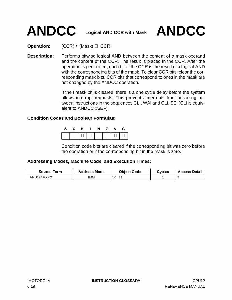
Operation: (CCR) • (Mask) ⇒ CCR
Description: Performs bitwise logical AND between the content of a mask operandand the content of the CCR. The result is placed in the CCR. After theoperation is performed, each bit of the CCR is the result of a logical ANDwith the corresponding bits of the mask. To clear CCR bits, clear the cor-responding mask bits. CCR bits that correspond to ones in the mask arenot changed by the ANDCC operation.
If the I mask bit is cleared, there is a one cycle delay before the systemallows interrupt requests. This prevents interrupts from occurring be-tween instructions in the sequences CLI, WAI and CLI, SEI (CLI is equiv-alent to ANDCC #$EF).
Condition Codes and Boolean Formulas:
Condition code bits are cleared if the corresponding bit was zero beforethe operation or if the corresponding bit in the mask is zero.
Addressing Modes, Machine Code, and Execution Times:
ANDCC Logical AND CCR with Mask ANDCC
S X H I N Z V C
⇓ ⇓ ⇓ ⇓ ⇓ ⇓ ⇓ ⇓
Source Form Address Mode Object Code Cycles Access DetailANDCC #opr8i IMM 10 ii 1 P
MOTOROLA INSTRUCTION GLOSSARY CPU12
6-18 REFERENCE MANUAL

Operation:
Description: Shifts all bits of memory location M one bit position to the left. Bit 0 isloaded with a zero. The C status bit is loaded from the most significantbit of M.
Condition Codes and Boolean Formulas:
Addressing Modes, Machine Code, and Execution Times:
ASL Arithmetic Shift Left Memory(same as LSL) ASL
S X H I N Z V C
– – – – ∆ ∆ ∆ ∆
N: Set if MSB of result is set; cleared otherwise.
Z: Set if result is $00; cleared otherwise.
V: N ⊕ C = [N • C] + [N • C] (for N and C after the shift)Set if (N is set and C is cleared) or (N is cleared and C is set); cleared oth-erwise (for values of N and C after the shift).
C: M7Set if the MSB of M was set before the shift; cleared otherwise.
Source Form Address Mode Object Code Cycles Access DetailASL opr16aASL oprx0_xyspASL oprx9,xyspASL oprx16,xyspASL [D,xysp]ASL [oprx16,xysp]
EXTIDXIDX1IDX2
[D,IDX][IDX2]
78 hh ll
68 xb
68 xb ff
68 xb ee ff
68 xb
68 xb ee ff
434566
rOPw
rPw
rPOw
frPPw
fIfrPw
fIPrPw
b7 – – – – – – b0 C 0
CPU12 INSTRUCTION GLOSSARY MOTOROLA
REFERENCE MANUAL 6-19

Operation:
Description: Shifts all bits of accumulator A one bit position to the left. Bit 0 is loadedwith a zero. The C status bit is loaded from the most significant bit of A.
Condition Codes and Boolean Formulas:
Addressing Modes, Machine Code, and Execution Times:
ASLA Arithmetic Shift Left A(same as LSLA) ASLA
S X H I N Z V C
– – – – ∆ ∆ ∆ ∆
N: Set if MSB of result is set; cleared otherwise.
Z: Set if result is $00; cleared otherwise.
V: N ⊕ C = [N • C] + [N • C] (for N and C after the shift)Set if (N is set and C is cleared) or (N is cleared and C is set); cleared oth-erwise (for values of N and C after the shift).
C: A7Set if the MSB of A was set before the shift; cleared otherwise.
Source Form Address Mode Object Code Cycles Access DetailASLA INH 48 1 O
b7 – – – – – – b0 C 0
MOTOROLA INSTRUCTION GLOSSARY CPU12
6-20 REFERENCE MANUAL

Operation:
Description: Shifts all bits of accumulator B one bit position to the left. Bit 0 is loadedwith a zero. The C status bit is loaded from the most significant bit of B.
Condition Codes and Boolean Formulas:
Addressing Modes, Machine Code, and Execution Times:
ASLB Arithmetic Shift Left B(same as LSLB) ASLB
S X H I N Z V C
– – – – ∆ ∆ ∆ ∆
N: Set if MSB of result is set; cleared otherwise.
Z: Set if result is $00; cleared otherwise.
V: N ⊕ C = [N • C] + [N • C] (for N and C after the shift)Set if (N is set and C is cleared) or (N is cleared and C is set); cleared other-wise (for values of N and C after the shift).
C: B7Set if the MSB of B was set before the shift; cleared otherwise.
Source Form Address Mode Object Code Cycles Access DetailASLB INH 58 1 O
b7 – – – – – – b0 C 0
CPU12 INSTRUCTION GLOSSARY MOTOROLA
REFERENCE MANUAL 6-21

Operation:
Description: Shifts all bits of double accumulator D one bit position to the left. Bit 0 isloaded with a zero. The C status bit is loaded from the most significantbit of D.
Condition Codes and Boolean Formulas:
Addressing Modes, Machine Code, and Execution Times:
ASLD Arithmetic Shift Left Double Accumulator(same as LSLD) ASLD
S X H I N Z V C
– – – – ∆ ∆ ∆ ∆
N: Set if MSB of result is set; cleared otherwise.
Z: Set if result is $0000; cleared otherwise.
V: N ⊕ C = [N • C] + [N • C] (for N and C after the shift)Set if (N is set and C is cleared) or (N is cleared and C is set); cleared oth-erwise (for values of N and C after the shift).
C: D15Set if the MSB of D was set before the shift; cleared otherwise.
Source Form Address Mode Object Code Cycles Access DetailASLD INH 59 1 O
b7 – – – – – – b0 C b7 – – – – – – b0A B
0
MOTOROLA INSTRUCTION GLOSSARY CPU12
6-22 REFERENCE MANUAL

Operation:
Description: Shifts all bits of memory location M one place to the right. Bit 7 is heldconstant. Bit 0 is loaded into the C status bit. This operation effectivelydivides a two’s complement value by two without changing its sign. Thecarry bit can be used to round the result.
Condition Codes and Boolean Formulas:
Addressing Modes, Machine Code, and Execution Times:
ASR Arithmetic Shift Right Memory ASR
S X H I N Z V C
– – – – ∆ ∆ ∆ ∆
N: Set if MSB of result is set; cleared otherwise.
Z: Set if result is $00; cleared otherwise.
V: N ⊕ C = [N • C] + [N • C] (for N and C after the shift)Set if (N is set and C is cleared) or (N is cleared and C is set); cleared other-wise (for values of N and C after the shift).
C: M0Set if the LSB of M was set before the shift; cleared otherwise.
Source Form Address Mode Object Code Cycles Access DetailASR opr16aASR oprx0_xyspASR oprx9,xyspASR oprx16,xyspASR [D,xysp]ASR [oprx16,xysp]
EXTIDXIDX1IDX2
[D,IDX][IDX2]
77 hh ll
67 xb
67 xb ff
67 xb ee ff
67 xb
67 xb ee ff
434566
rOPw
rPw
rPOw
frPPw
fIfrPw
fIPrPw
b7 – – – – – – b0 C
CPU12 INSTRUCTION GLOSSARY MOTOROLA
REFERENCE MANUAL 6-23

Operation:
Description: Shifts all bits of accumulator A one place to the right. Bit 7 is held con-stant. Bit 0 is loaded into the C status bit. This operation effectively di-vides a two’s complement value by two without changing its sign. Thecarry bit can be used to round the result.
Condition Codes and Boolean Formulas:
Addressing Modes, Machine Code, and Execution Times:
ASRA Arithmetic Shift Right A ASRA
S X H I N Z V C
– – – – ∆ ∆ ∆ ∆
N: Set if MSB of result is set; cleared otherwise.
Z: Set if result is $00; cleared otherwise.
V: N ⊕ C = [N • C] + [N • C] (for N and C after the shift)Set if (N is set and C is cleared) or (N is cleared and C is set); cleared oth-erwise (for values of N and C after the shift).
C: A0Set if the LSB of A was set before the shift; cleared otherwise.
Source Form Address Mode Object Code Cycles Access DetailASRA INH 47 1 O
b7 – – – – – – b0 C
MOTOROLA INSTRUCTION GLOSSARY CPU12
6-24 REFERENCE MANUAL

Operation:
Description: Shifts all bits of accumulator B one place to the right. Bit 7 is held con-stant. Bit 0 is loaded into the C status bit. This operation effectively di-vides a two’s complement value by two without changing its sign. Thecarry bit can be used to round the result.
Condition Codes and Boolean Formulas:
Addressing Modes, Machine Code, and Execution Times:
ASRB Arithmetic Shift Right B ASRB
S X H I N Z V C
– – – – ∆ ∆ ∆ ∆
N: Set if MSB of result is set; cleared otherwise.
Z: Set if result is $00; cleared otherwise.
V: N ⊕ C = [N • C] + [N • C] (for N and C after the shift)Set if (N is set and C is cleared) or (N is cleared and C is set); cleared oth-erwise (for values of N and C after the shift).
C: B0Set if the LSB of B was set before the shift; cleared otherwise.
Source Form Address Mode Object Code Cycles Access DetailASRB INH 57 1 O
b7 – – – – – – b0 C
CPU12 INSTRUCTION GLOSSARY MOTOROLA
REFERENCE MANUAL 6-25

Operation: If C = 0, then (PC) + $0002 + Rel ⇒ PC
Simple branch
Description: Tests the C status bit and branches if C = 0.
See 3.7 Relative Addressing Mode for details of branch execution.
Condition Codes and Boolean Formulas:
None affected.
Addressing Modes, Machine Code, and Execution Times:
BCC Branch if Carry Cleared(Same as BHS) BCC
S X H I N Z V C
– – – – – – – –
Source Form Address Mode Object Code Cycles Access DetailBCC rel8 REL 24 rr 3 /1 PPP/P1
Notes:1. PPP/P indicates this instruction takes three cycles to refill the instruction queue if the branch is taken and one
program fetch cycle if the branch is not taken.
Branch Complementary BranchTest Mnemonic Opcode Boolean Test Mnemonic Opcode Commentr>m BGT 2E Z + (N ⊕ V) = 0 r≤m BLE 2F Signedr≥m BGE 2C N ⊕ V = 0 r<m BLT 2D Signedr=m BEQ 27 Z = 1 r≠m BNE 26 Signedr≤m BLE 2F Z + (N ⊕ V) = 1 r>m BGT 2E Signedr<m BLT 2D N ⊕ V = 1 r≥m BGE 2C Signedr>m BHI 22 C + Z = 0 r≤m BLS 23 Unsignedr≥m BHS/BCC 24 C = 0 r<m BLO/BCS 25 Unsignedr=m BEQ 27 Z = 1 r≠m BNE 26 Unsignedr≤m BLS 23 C + Z = 1 r>m BHI 22 Unsignedr<m BLO/BCS 25 C = 1 r≥m BHS/BCC 24 Unsigned
Carry BCS 25 C = 1 No Carry BCC 24 SimpleNegative BMI 2B N = 1 Plus BPL 2A SimpleOverflow BVS 29 V = 1 No Overflow BVC 28 Simple
r=0 BEQ 27 Z = 1 r≠0 BNE 26 SimpleAlways BRA 20 — Never BRN 21 Unconditional
MOTOROLA INSTRUCTION GLOSSARY CPU12
6-26 REFERENCE MANUAL

Operation: (M) • (Mask) ⇒ M
Description: Clears bits in location M. To clear a bit, set the corresponding bit in themask byte. Bits in M that correspond to zeros in the mask byte are notchanged. Mask bytes can be located at PC + 2, PC + 3, or PC + 4, de-pending on addressing mode used.
Condition Codes and Boolean Formulas:
Addressing Modes, Machine Code, and Execution Times:
BCLR Clear Bits in Memory BCLR
S X H I N Z V C
– – – – ∆ ∆ 0 –
N: Set if MSB of result is set; cleared otherwise.
Z: Set if result is $00; cleared otherwise.
V: 0; Cleared.
Source Form Address Mode 1
Notes:1. Indirect forms of indexed addressing cannot be used with this instruction.
Object Code Cycles Access DetailBCLR opr8a, msk8BCLR opr16a, msk8BCLR oprx0_xysp, msk8BCLR oprx9,xysp, msk8BCLR oprx16,xysp, msk8
DIREXTIDXIDX1IDX2
4D dd mm
1D hh ll mm
0D xb mm
0D xb ff mm
0D xb ee ff mm
44446
rPOw
rPPw
rPOw
rPwP
frPwOP
CPU12 INSTRUCTION GLOSSARY MOTOROLA
REFERENCE MANUAL 6-27

Operation: If C = 1, then (PC) + $0002 + Rel ⇒ PC
Simple branch
Description: Tests the C status bit and branches if C = 1.
See 3.7 Relative Addressing Mode for details of branch execution.
Condition Codes and Boolean Formulas:
None affected.
Addressing Modes, Machine Code, and Execution Times:
BCS Branch if Carry Set(Same as BLO) BCS
S X H I N Z V C
– – – – – – – –
Source Form Address Mode Object Code Cycles Access DetailBCS rel8 REL 25 rr 3/1 PPP/P1
Notes:1. PPP/P indicates this instruction takes three cycles to refill the instruction queue if the branch is taken and one
program fetch cycle if the branch is not taken.
Branch Complementary BranchTest Mnemonic Opcode Boolean Test Mnemonic Opcode Commentr>m BGT 2E Z + (N ⊕ V) = 0 r≤m BLE 2F Signedr≥m BGE 2C N ⊕ V = 0 r<m BLT 2D Signedr=m BEQ 27 Z = 1 r≠m BNE 26 Signedr≤m BLE 2F Z + (N ⊕ V) = 1 r>m BGT 2E Signedr<m BLT 2D N ⊕ V = 1 r≥m BGE 2C Signedr>m BHI 22 C + Z = 0 r≤m BLS 23 Unsignedr≥m BHS/BCC 24 C = 0 r<m BLO/BCS 25 Unsignedr=m BEQ 27 Z = 1 r≠m BNE 26 Unsignedr≤m BLS 23 C + Z = 1 r>m BHI 22 Unsignedr<m BLO/BCS 25 C = 1 r≥m BHS/BCC 24 Unsigned
Carry BCS 25 C = 1 No Carry BCC 24 SimpleNegative BMI 2B N = 1 Plus BPL 2A SimpleOverflow BVS 29 V = 1 No Overflow BVC 28 Simple
r=0 BEQ 27 Z = 1 r≠0 BNE 26 SimpleAlways BRA 20 — Never BRN 21 Unconditional
MOTOROLA INSTRUCTION GLOSSARY CPU12
6-28 REFERENCE MANUAL

Operation: If Z = 1, then (PC) + $0002 + Rel ⇒ PC
Simple branch
Description: Tests the Z status bit and branches if Z = 1.
See 3.7 Relative Addressing Mode for details of branch execution.
Condition Codes and Boolean Formulas:
None affected.
Addressing Modes, Machine Code, and Execution Times:
BEQ Branch if Equal BEQ
S X H I N Z V C
– – – – – – – –
Source Form Address Mode Object Code Cycles Access DetailBEQ rel8 REL 27 rr 3/1 PPP/P1
Notes:1. PPP/P indicates this instruction takes three cycles to refill the instruction queue if the branch is taken and one
program fetch cycle if the branch is not taken.
Branch Complementary BranchTest Mnemonic Opcode Boolean Test Mnemonic Opcode Commentr>m BGT 2E Z + (N ⊕ V) = 0 r≤m BLE 2F Signedr≥m BGE 2C N ⊕ V = 0 r<m BLT 2D Signedr=m BEQ 27 Z = 1 r≠m BNE 26 Signedr≤m BLE 2F Z + (N ⊕ V) = 1 r>m BGT 2E Signedr<m BLT 2D N ⊕ V = 1 r≥m BGE 2C Signedr>m BHI 22 C + Z = 0 r≤m BLS 23 Unsignedr≥m BHS/BCC 24 C = 0 r<m BLO/BCS 25 Unsignedr=m BEQ 27 Z = 1 r≠m BNE 26 Unsignedr≤m BLS 23 C + Z = 1 r>m BHI 22 Unsignedr<m BLO/BCS 25 C = 1 r≥m BHS/BCC 24 Unsigned
Carry BCS 25 C = 1 No Carry BCC 24 SimpleNegative BMI 2B N = 1 Plus BPL 2A SimpleOverflow BVS 29 V = 1 No Overflow BVC 28 Simple
r=0 BEQ 27 Z = 1 r≠0 BNE 26 SimpleAlways BRA 20 — Never BRN 21 Unconditional
CPU12 INSTRUCTION GLOSSARY MOTOROLA
REFERENCE MANUAL 6-29

Operation: If N ⊕ V = 0, then (PC) + $0002 + Rel ⇒ PC
For signed two’s complement valuesif (Accumulator) ≥ (Memory), then branch
Description: If BGE is executed immediately after execution of CBA, CMPA, CMPB,CMPD, CPX, CPY, SBA, SUBA, SUBB, or SUBD, a branch occurs if andonly if the signed two’s complement number in the accumulator is great-er than or equal to the signed two’s complement number in memory.
See 3.7 Relative Addressing Mode for details of branch execution.
Condition Codes and Boolean Formulas:
None affected.
Addressing Modes, Machine Code, and Execution Times:
BGE Branch if Greater than or Equal to Zero BGE
S X H I N Z V C
– – – – – – – –
Source Form Address Mode Object Code Cycles Access DetailBGE rel8 REL 2C rr 3/1 PPP/P1
Notes:1. PPP/P indicates this instruction takes three cycles to refill the instruction queue if the branch is taken and one
program fetch cycle if the branch is not taken.
Branch Complementary BranchTest Mnemonic Opcode Boolean Test Mnemonic Opcode Commentr>m BGT 2E Z + (N ⊕ V) = 0 r≤m BLE 2F Signedr≥m BGE 2C N ⊕ V = 0 r<m BLT 2D Signedr=m BEQ 27 Z = 1 r≠m BNE 26 Signedr≤m BLE 2F Z + (N ⊕ V) = 1 r>m BGT 2E Signedr<m BLT 2D N ⊕ V = 1 r≥m BGE 2C Signedr>m BHI 22 C + Z = 0 r≤m BLS 23 Unsignedr≥m BHS/BCC 24 C = 0 r<m BLO/BCS 25 Unsignedr=m BEQ 27 Z = 1 r≠m BNE 26 Unsignedr≤m BLS 23 C + Z = 1 r>m BHI 22 Unsignedr<m BLO/BCS 25 C = 1 r≥m BHS/BCC 24 Unsigned
Carry BCS 25 C = 1 No Carry BCC 24 SimpleNegative BMI 2B N = 1 Plus BPL 2A SimpleOverflow BVS 29 V = 1 No Overflow BVC 28 Simple
r=0 BEQ 27 Z = 1 r≠0 BNE 26 SimpleAlways BRA 20 — Never BRN 21 Unconditional
MOTOROLA INSTRUCTION GLOSSARY CPU12
6-30 REFERENCE MANUAL

Description: BGND operates like a software interrupt, except that no registers arestacked. First, the current PC value is stored in internal CPU registerTMP2. Next, the BDM ROM and background register block become ac-tive. The BDM ROM contains a substitute vector, mapped to the addressof the software interrupt vector, which points to routines in the BDMROM that control background operation. The substitute vector isfetched, and execution continues from the address that it points to. Fi-nally, the CPU checks the location that TMP2 points to. If the valuestored in that location is $00 (the BGND opcode), TMP2 is incremented,so that the instruction that follows the BGND instruction is the first in-struction executed when normal program execution resumes.
For all other types of BDM entry, the CPU performs the same sequenceof operations as for a BGND instruction, but the value stored in TMP2already points to the instruction that would have executed next had BDMnot become active. If active BDM is triggered just as a BGND instructionis about to execute, the BDM firmware does increment TMP2, but thechange does not affect resumption of normal execution.
While BDM is active, the CPU executes debugging commands receivedvia a special single-wire serial interface. BDM is terminated by the exe-cution of specific debugging commands. Upon exit from BDM, the back-ground/boot ROM and registers are disabled, the instruction queue isrefilled starting with the return address pointed to by TMP2, and normalprocessing resumes.
BDM is normally disabled to avoid accidental entry. While BDM is dis-abled, BGND executes as described, but the firmware causes executionto return to the user program. Refer to SECTION 8 DEVELOPMENTAND DEBUG SUPPORT for more information concerning BDM.
Condition Codes and Boolean Formulas:
None affected.
Addressing Modes, Machine Code, and Execution Times:
BGND Enter Background Debug Mode BGND
S X H I N Z V C
– – – – – – – –
Source Form Address Mode Object Code Cycles Access DetailBGND INH 00 5 VfPPP
CPU12 INSTRUCTION GLOSSARY MOTOROLA
REFERENCE MANUAL 6-31

Operation: If Z + (N ⊕ V) = 0, then (PC) + $0002 + Rel ⇒ PC
For signed two’s complement valuesif (Accumulator) > (Memory), then branch
Description: If BGT is executed immediately after execution of CBA, CMPA, CMPB,CMPD, CPX, CPY, SBA, SUBA, SUBB, or SUBD, a branch occurs if andonly if the signed two’s complement number in the accumulator is great-er than the signed two’s complement number in memory.
See 3.7 Relative Addressing Mode for details of branch execution.
Condition Codes and Boolean Formulas:
None affected.
Addressing Modes, Machine Code, and Execution Times:
BGT Branch if Greater than Zero BGT
S X H I N Z V C
– – – – – – – –
Source Form Address Mode Object Code Cycles Access DetailBGT rel8 REL 2E rr 3/1 PPP/P1
Notes:1. PPP/P indicates this instruction takes three cycles to refill the instruction queue if the branch is taken and one
program fetch cycle if the branch is not taken.
Branch Complementary BranchTest Mnemonic Opcode Boolean Test Mnemonic Opcode Commentr>m BGT 2E Z + (N ⊕ V) = 0 r≤m BLE 2F Signedr≥m BGE 2C N ⊕ V = 0 r<m BLT 2D Signedr=m BEQ 27 Z = 1 r≠m BNE 26 Signedr≤m BLE 2F Z + (N ⊕ V) = 1 r>m BGT 2E Signedr<m BLT 2D N ⊕ V = 1 r≥m BGE 2C Signedr>m BHI 22 C + Z = 0 r≤m BLS 23 Unsignedr≥m BHS/BCC 24 C = 0 r<m BLO/BCS 25 Unsignedr=m BEQ 27 Z = 1 r≠m BNE 26 Unsignedr≤m BLS 23 C + Z = 1 r>m BHI 22 Unsignedr<m BLO/BCS 25 C = 1 r≥m BHS/BCC 24 Unsigned
Carry BCS 25 C = 1 No Carry BCC 24 SimpleNegative BMI 2B N = 1 Plus BPL 2A SimpleOverflow BVS 29 V = 1 No Overflow BVC 28 Simple
r=0 BEQ 27 Z = 1 r≠0 BNE 26 SimpleAlways BRA 20 — Never BRN 21 Unconditional
MOTOROLA INSTRUCTION GLOSSARY CPU12
6-32 REFERENCE MANUAL

Operation: If C + Z = 0, then (PC) + $0002 + Rel ⇒ PC
For unsigned values, if (Accumulator) > (Memory), then branch
Description: If BHI is executed immediately after execution of CBA, CMPA, CMPB,CMPD, CPX, CPY, SBA, SUBA, SUBB, or SUBD, a branch occurs if andonly if the unsigned binary number in the accumulator was greater thanthe unsigned binary number in memory. Generally not useful after INC/DEC, LD/ST, TST/CLR/COM because these instructions do not affectthe C status bit.
See 3.7 Relative Addressing Mode for details of branch execution.
Condition Codes and Boolean Formulas:
None affected.
Addressing Modes, Machine Code, and Execution Times:
BHI Branch if Higher BHI
S X H I N Z V C
– – – – – – – –
Source Form Address Mode Object Code Cycles Access DetailBHI rel8 REL 22 rr 3/1 PPP/P1
Notes:1. PPP/P indicates this instruction takes three cycles to refill the instruction queue if the branch is taken and one
program fetch cycle if the branch is not taken.
Branch Complementary BranchTest Mnemonic Opcode Boolean Test Mnemonic Opcode Commentr>m BGT 2E Z + (N ⊕ V) = 0 r≤m BLE 2F Signedr≥m BGE 2C N ⊕ V = 0 r<m BLT 2D Signedr=m BEQ 27 Z = 1 r≠m BNE 26 Signedr≤m BLE 2F Z + (N ⊕ V) = 1 r>m BGT 2E Signedr<m BLT 2D N ⊕ V = 1 r≥m BGE 2C Signedr>m BHI 22 C + Z = 0 r≤m BLS 23 Unsignedr≥m BHS/BCC 24 C = 0 r<m BLO/BCS 25 Unsignedr=m BEQ 27 Z = 1 r≠m BNE 26 Unsignedr≤m BLS 23 C + Z = 1 r>m BHI 22 Unsignedr<m BLO/BCS 25 C = 1 r≥m BHS/BCC 24 Unsigned
Carry BCS 25 C = 1 No Carry BCC 24 SimpleNegative BMI 2B N = 1 Plus BPL 2A SimpleOverflow BVS 29 V = 1 No Overflow BVC 28 Simple
r=0 BEQ 27 Z = 1 r≠0 BNE 26 SimpleAlways BRA 20 — Never BRN 21 Unconditional
CPU12 INSTRUCTION GLOSSARY MOTOROLA
REFERENCE MANUAL 6-33

Operation: If C = 0, then (PC) + $0002 + Rel ⇒ PC
For unsigned values, if (Accumulator) ≥ (Memory), then branch
Description: If BHS is executed immediately after execution of CBA, CMPA, CMPB,CMPD, CPX, CPY, SBA, SUBA, SUBB, or SUBD, a branch occurs if andonly if the unsigned binary number in the accumulator was greater thanthe unsigned binary number in memory. Generally not useful after INC/DEC, LD/ST, TST/CLR/COM because these instructions do not affectthe C status bit.
See 3.7 Relative Addressing Mode for details of branch execution.
Condition Codes and Boolean Formulas:
None affected.
Addressing Modes, Machine Code, and Execution Times:
BHS Branch if Higher or Same(Same as BCC) BHS
S X H I N Z V C
– – – – – – – –
Source Form Address Mode Object Code Cycles Access DetailBHS rel8 REL 24 rr 3/1 PPP/P1
Notes:1. PPP/P indicates this instruction takes three cycles to refill the instruction queue if the branch is taken and one
program fetch cycle if the branch is not taken.
Branch Complementary BranchTest Mnemonic Opcode Boolean Test Mnemonic Opcode Commentr>m BGT 2E Z + (N ⊕ V) = 0 r≤m BLE 2F Signedr≥m BGE 2C N ⊕ V = 0 r<m BLT 2D Signedr=m BEQ 27 Z = 1 r≠m BNE 26 Signedr≤m BLE 2F Z + (N ⊕ V) = 1 r>m BGT 2E Signedr<m BLT 2D N ⊕ V = 1 r≥m BGE 2C Signedr>m BHI 22 C + Z = 0 r≤m BLS 23 Unsignedr≥m BHS/BCC 24 C = 0 r<m BLO/BCS 25 Unsignedr=m BEQ 27 Z = 1 r≠m BNE 26 Unsignedr≤m BLS 23 C + Z = 1 r>m BHI 22 Unsignedr<m BLO/BCS 25 C = 1 r≥m BHS/BCC 24 Unsigned
Carry BCS 25 C = 1 No Carry BCC 24 SimpleNegative BMI 2B N = 1 Plus BPL 2A SimpleOverflow BVS 29 V = 1 No Overflow BVC 28 Simple
r=0 BEQ 27 Z = 1 r≠0 BNE 26 SimpleAlways BRA 20 — Never BRN 21 Unconditional
MOTOROLA INSTRUCTION GLOSSARY CPU12
6-34 REFERENCE MANUAL

Operation: (A) • (M)
Description: Performs bitwise logical AND on the content of accumulator A and thecontent of memory location M, and modifies the condition codes accord-ingly. Each bit of the result is the logical AND of the corresponding bitsof the accumulator and the memory location. Neither the content of theaccumulator nor the content of the memory location is affected.
Condition Codes and Boolean Formulas:
Addressing Modes, Machine Code, and Execution Times:
BITA Bit Test A BITA
S X H I N Z V C
– – – – ∆ ∆ 0 –
N: Set if MSB of result is set; cleared otherwise.
Z: Set if result is $00; cleared otherwise.
V: 0; Cleared.
Source Form Address Mode Object Code Cycles Access DetailBITA #opr8iBITA opr8aBITA opr16aBITA oprx0_xyspBITA oprx9,xyspBITA oprx16,xyspBITA [D,xysp]BITA [oprx16,xysp]
IMMDIREXTIDXIDX1IDX2
[D,IDX][IDX2]
85 ii
95 dd
B5 hh ll
A5 xb
A5 xb ff
A5 xb ee ff
A5 xb
A5 xb ee ff
13333466
P
rfP
rOP
rfP
rPO
frPP
fIfrfP
fIPrfP
CPU12 INSTRUCTION GLOSSARY MOTOROLA
REFERENCE MANUAL 6-35

Operation: (B) • (M)
Description: Performs bitwise logical AND on the content of accumulator B and thecontent of memory location M, and modifies the condition codes accord-ingly. Each bit of the result is the logical AND of the corresponding bitsof the accumulator and the memory location. Neither the content of theaccumulator nor the content of the memory location is affected.
Condition Codes and Boolean Formulas:
Addressing Modes, Machine Code, and Execution Times:
BITB Bit Test B BITB
S X H I N Z V C
– – – – ∆ ∆ 0 –
N: Set if MSB of result is set; cleared otherwise.
Z: Set if result is $00; cleared otherwise.
V: 0; Cleared.
Source Form Address Mode Object Code Cycles Access DetailBITB #opr8iBITB opr8aBITB opr16aBITB oprx0_xyspBITB oprx9,xyspBITB oprx16,xyspBITB [D,xysp]BITB [oprx16,xysp]
IMMDIREXTIDXIDX1IDX2
[D,IDX][IDX2]
C5 ii
D5 dd
F5 hh ll
E5 xb
E5 xb ff
E5 xb ee ff
E5 xb
E5 xb ee ff
13333466
P
rfP
rOP
rfP
rPO
frPP
fIfrfP
fIPrfP
MOTOROLA INSTRUCTION GLOSSARY CPU12
6-36 REFERENCE MANUAL

Operation: If Z + (N ⊕ V) = 1, then (PC) + $0002 + Rel ⇒ PC
For signed two’s complement numbersif (Accumulator) ≤ (Memory), then branch
Description: If BLE is executed immediately after execution of CBA, CMPA, CMPB,CMPD, CPX, CPY, SBA, SUBA, SUBB, or SUBD, a branch occurs if andonly if the two’s complement number in the accumulator was less thanor equal to the two’s complement number in memory.
See 3.7 Relative Addressing Mode for details of branch execution.
Condition Codes and Boolean Formulas:
None affected.
Addressing Modes, Machine Code, and Execution Times:
BLE Branch if Less Than or Equal to Zero BLE
S X H I N Z V C
– – – – – – – –
Source Form Address Mode Object Code Cycles Access DetailBLE rel8 REL 2F rr 3/1 PPP/P1
Notes:1. PPP/P indicates this instruction takes three cycles to refill the instruction queue if the branch is taken and one
program fetch cycle if the branch is not taken.
Branch Complementary BranchTest Mnemonic Opcode Boolean Test Mnemonic Opcode Commentr>m BGT 2E Z + (N ⊕ V) = 0 r≤m BLE 2F Signedr≥m BGE 2C N ⊕ V = 0 r<m BLT 2D Signedr=m BEQ 27 Z = 1 r≠m BNE 26 Signedr≤m BLE 2F Z + (N ⊕ V) = 1 r>m BGT 2E Signedr<m BLT 2D N ⊕ V = 1 r≥m BGE 2C Signedr>m BHI 22 C + Z = 0 r≤m BLS 23 Unsignedr≥m BHS/BCC 24 C = 0 r<m BLO/BCS 25 Unsignedr=m BEQ 27 Z = 1 r≠m BNE 26 Unsignedr≤m BLS 23 C + Z = 1 r>m BHI 22 Unsignedr<m BLO/BCS 25 C = 1 r≥m BHS/BCC 24 Unsigned
Carry BCS 25 C = 1 No Carry BCC 24 SimpleNegative BMI 2B N = 1 Plus BPL 2A SimpleOverflow BVS 29 V = 1 No Overflow BVC 28 Simple
r=0 BEQ 27 Z = 1 r≠0 BNE 26 SimpleAlways BRA 20 — Never BRN 21 Unconditional
CPU12 INSTRUCTION GLOSSARY MOTOROLA
REFERENCE MANUAL 6-37

Operation: If C = 1, then (PC) + $0002 + Rel ⇒ PC
For unsigned values, if (Accumulator) < (Memory), then branch
Description: If BLO is executed immediately after execution of CBA, CMPA, CMPB,CMPD, CPX, CPY, SBA, SUBA, SUBB, or SUBD, a branch occurs if andonly if the unsigned binary number in the accumulator is less than theunsigned binary number in memory. Generally not useful after INC/DEC,LD/ST, TST/CLR/COM because these instructions do not affect the Cstatus bit.
See 3.7 Relative Addressing Mode for details of branch execution.
Condition Codes and Boolean Formulas:
None affected.
Addressing Modes, Machine Code, and Execution Times:
BLO Branch if Lower(Same as BCS) BLO
S X H I N Z V C
– – – – – – – –
Source Form Address Mode Object Code Cycles Access DetailBLO rel8 REL 25 rr 3/1 PPP/P1
Notes:1. PPP/P indicates this instruction takes three cycles to refill the instruction queue if the branch is taken and one
program fetch cycle if the branch is not taken.
Branch Complementary BranchTest Mnemonic Opcode Boolean Test Mnemonic Opcode Commentr>m BGT 2E Z + (N ⊕ V) = 0 r≤m BLE 2F Signedr≥m BGE 2C N ⊕ V = 0 r<m BLT 2D Signedr=m BEQ 27 Z = 1 r≠m BNE 26 Signedr≤m BLE 2F Z + (N ⊕ V) = 1 r>m BGT 2E Signedr<m BLT 2D N ⊕ V = 1 r≥m BGE 2C Signedr>m BHI 22 C + Z = 0 r≤m BLS 23 Unsignedr≥m BHS/BCC 24 C = 0 r<m BLO/BCS 25 Unsignedr=m BEQ 27 Z = 1 r≠m BNE 26 Unsignedr≤m BLS 23 C + Z = 1 r>m BHI 22 Unsignedr<m BLO/BCS 25 C = 1 r≥m BHS/BCC 24 Unsigned
Carry BCS 25 C = 1 No Carry BCC 24 SimpleNegative BMI 2B N = 1 Plus BPL 2A SimpleOverflow BVS 29 V = 1 No Overflow BVC 28 Simple
r=0 BEQ 27 Z = 1 r≠0 BNE 26 SimpleAlways BRA 20 — Never BRN 21 Unconditional
MOTOROLA INSTRUCTION GLOSSARY CPU12
6-38 REFERENCE MANUAL

Operation: If C + Z = 1, then (PC) + $0002 + Rel ⇒ PC
For unsigned values, if (Accumulator) ≤ (Memory), then branch
Description: If BLS is executed immediately after execution of CBA, CMPA, CMPB,CMPD, CPX, CPY, SBA, SUBA, SUBB, or SUBD, a branch occurs if andonly if the unsigned binary number in the accumulator is less than orequal to the unsigned binary number in memory. Generally not usefulafter INC/DEC, LD/ST, TST/CLR/COM because these instructions donot affect the C status bit.
See 3.7 Relative Addressing Mode for details of branch execution.
Condition Codes and Boolean Formulas:
None affected.
Addressing Modes, Machine Code, and Execution Times:
BLS Branch if Lower or Same BLS
S X H I N Z V C
– – – – – – – –
Source Form Address Mode Object Code Cycles Access DetailBLS rel8 REL 23 rr 3/1 PPP/P1
Notes:1. PPP/P indicates this instruction takes three cycles to refill the instruction queue if the branch is taken and one
program fetch cycle if the branch is not taken.
Branch Complementary BranchTest Mnemonic Opcode Boolean Test Mnemonic Opcode Commentr>m BGT 2E Z + (N ⊕ V) = 0 r≤m BLE 2F Signedr≥m BGE 2C N ⊕ V = 0 r<m BLT 2D Signedr=m BEQ 27 Z = 1 r≠m BNE 26 Signedr≤m BLE 2F Z + (N ⊕ V) = 1 r>m BGT 2E Signedr<m BLT 2D N ⊕ V = 1 r≥m BGE 2C Signedr>m BHI 22 C + Z = 0 r≤m BLS 23 Unsignedr≥m BHS/BCC 24 C = 0 r<m BLO/BCS 25 Unsignedr=m BEQ 27 Z = 1 r≠m BNE 26 Unsignedr≤m BLS 23 C + Z = 1 r>m BHI 22 Unsignedr<m BLO/BCS 25 C = 1 r≥m BHS/BCC 24 Unsigned
Carry BCS 25 C = 1 No Carry BCC 24 SimpleNegative BMI 2B N = 1 Plus BPL 2A SimpleOverflow BVS 29 V = 1 No Overflow BVC 28 Simple
r=0 BEQ 27 Z = 1 r≠0 BNE 26 SimpleAlways BRA 20 — Never BRN 21 Unconditional
CPU12 INSTRUCTION GLOSSARY MOTOROLA
REFERENCE MANUAL 6-39

Operation: If N ⊕ V = 1, then (PC) + $0002 + Rel ⇒ PC
For signed two’s complement numbersif (Accumulator) < (Memory), then branch
Description: If BLT is executed immediately after execution of CBA, CMPA, CMPB,CMPD, CPX, CPY, SBA, SUBA, SUBB, or SUBD, a branch occurs if andonly if the two’s complement number in the accumulator is less than thetwo’s complement number in memory.
See 3.7 Relative Addressing Mode for details of branch execution.
Condition Codes and Boolean Formulas:
None affected.
Addressing Modes, Machine Code, and Execution Times:
BLT Branch if Less than Zero BLT
S X H I N Z V C
– – – – – – – –
Source Form Address Mode Object Code Cycles Access DetailBLT rel8 REL 2D rr 3/1 PPP/P1
Notes:1. PPP/P indicates this instruction takes three cycles to refill the instruction queue if the branch is taken and one
program fetch cycle if the branch is not taken.
Branch Complementary BranchTest Mnemonic Opcode Boolean Test Mnemonic Opcode Commentr>m BGT 2E Z + (N ⊕ V) = 0 r≤m BLE 2F Signedr≥m BGE 2C N ⊕ V = 0 r<m BLT 2D Signedr=m BEQ 27 Z = 1 r≠m BNE 26 Signedr≤m BLE 2F Z + (N ⊕ V) = 1 r>m BGT 2E Signedr<m BLT 2D N ⊕ V = 1 r≥m BGE 2C Signedr>m BHI 22 C + Z = 0 r≤m BLS 23 Unsignedr≥m BHS/BCC 24 C = 0 r<m BLO/BCS 25 Unsignedr=m BEQ 27 Z = 1 r≠m BNE 26 Unsignedr≤m BLS 23 C + Z = 1 r>m BHI 22 Unsignedr<m BLO/BCS 25 C = 1 r≥m BHS/BCC 24 Unsigned
Carry BCS 25 C = 1 No Carry BCC 24 SimpleNegative BMI 2B N = 1 Plus BPL 2A SimpleOverflow BVS 29 V = 1 No Overflow BVC 28 Simple
r=0 BEQ 27 Z = 1 r≠0 BNE 26 SimpleAlways BRA 20 — Never BRN 21 Unconditional
MOTOROLA INSTRUCTION GLOSSARY CPU12
6-40 REFERENCE MANUAL

Operation: If N = 1, then (PC) + $0002 + Rel ⇒ PC
Simple branch
Description: Tests the N status bit and branches if N = 1.
See 3.7 Relative Addressing Mode for details of branch execution.
Condition Codes and Boolean Formulas:
None affected.
Addressing Modes, Machine Code, and Execution Times:
BMI Branch if Minus BMI
S X H I N Z V C
– – – – – – – –
Source Form Address Mode Object Code Cycles Access DetailBMI rel8 REL 2B rr 3/1 PPP/P1
Notes:1. PPP/P indicates this instruction takes three cycles to refill the instruction queue if the branch is taken and one
program fetch cycle if the branch is not taken.
Branch Complementary BranchTest Mnemonic Opcode Boolean Test Mnemonic Opcode Commentr>m BGT 2E Z + (N ⊕ V) = 0 r≤m BLE 2F Signedr≥m BGE 2C N ⊕ V = 0 r<m BLT 2D Signedr=m BEQ 27 Z = 1 r≠m BNE 26 Signedr≤m BLE 2F Z + (N ⊕ V) = 1 r>m BGT 2E Signedr<m BLT 2D N ⊕ V = 1 r≥m BGE 2C Signedr>m BHI 22 C + Z = 0 r≤m BLS 23 Unsignedr≥m BHS/BCC 24 C = 0 r<m BLO/BCS 25 Unsignedr=m BEQ 27 Z = 1 r≠m BNE 26 Unsignedr≤m BLS 23 C + Z = 1 r>m BHI 22 Unsignedr<m BLO/BCS 25 C = 1 r≥m BHS/BCC 24 Unsigned
Carry BCS 25 C = 1 No Carry BCC 24 SimpleNegative BMI 2B N = 1 Plus BPL 2A SimpleOverflow BVS 29 V = 1 No Overflow BVC 28 Simple
r=0 BEQ 27 Z = 1 r≠0 BNE 26 SimpleAlways BRA 20 — Never BRN 21 Unconditional
CPU12 INSTRUCTION GLOSSARY MOTOROLA
REFERENCE MANUAL 6-41

Operation: If Z = 0, then (PC) + $0002 + Rel ⇒ PC
Simple branch
Description: Tests the Z status bit and branches if Z = 0.
See 3.7 Relative Addressing Mode for details of branch execution.
Condition Codes and Boolean Formulas:
None affected.
Addressing Modes, Machine Code, and Execution Times:
BNE Branch if Not Equal to Zero BNE
S X H I N Z V C
– – – – – – – –
Source Form Address Mode Object Code Cycles Access DetailBNE rel8 REL 26 rr 3/1 PPP/P1
Notes:1. PPP/P indicates this instruction takes three cycles to refill the instruction queue if the branch is taken and one
program fetch cycle if the branch is not taken.
Branch Complementary BranchTest Mnemonic Opcode Boolean Test Mnemonic Opcode Commentr>m BGT 2E Z + (N ⊕ V) = 0 r≤m BLE 2F Signedr≥m BGE 2C N ⊕ V = 0 r<m BLT 2D Signedr=m BEQ 27 Z = 1 r≠m BNE 26 Signedr≤m BLE 2F Z + (N ⊕ V) = 1 r>m BGT 2E Signedr<m BLT 2D N ⊕ V = 1 r≥m BGE 2C Signedr>m BHI 22 C + Z = 0 r≤m BLS 23 Unsignedr≥m BHS/BCC 24 C = 0 r<m BLO/BCS 25 Unsignedr=m BEQ 27 Z = 1 r≠m BNE 26 Unsignedr≤m BLS 23 C + Z = 1 r>m BHI 22 Unsignedr<m BLO/BCS 25 C = 1 r≥m BHS/BCC 24 Unsigned
Carry BCS 25 C = 1 No Carry BCC 24 SimpleNegative BMI 2B N = 1 Plus BPL 2A SimpleOverflow BVS 29 V = 1 No Overflow BVC 28 Simple
r=0 BEQ 27 Z = 1 r≠0 BNE 26 SimpleAlways BRA 20 — Never BRN 21 Unconditional
MOTOROLA INSTRUCTION GLOSSARY CPU12
6-42 REFERENCE MANUAL

Operation: If N = 0, then (PC) + $0002 + Rel ⇒ PC
Simple branch
Description: Tests the N status bit and branches if N = 0.
See 3.7 Relative Addressing Mode for details of branch execution.
Condition Codes and Boolean Formulas:
None affected.
Addressing Modes, Machine Code, and Execution Times:
BPL Branch if Plus BPL
S X H I N Z V C
– – – – – – – –
Source Form Address Mode Object Code Cycles Access DetailBPL rel8 REL 2A rr 3/1 PPP/P1
Notes:1. PPP/P indicates this instruction takes three cycles to refill the instruction queue if the branch is taken and one
program fetch cycle if the branch is not taken.
Branch Complementary BranchTest Mnemonic Opcode Boolean Test Mnemonic Opcode Commentr>m BGT 2E Z + (N ⊕ V) = 0 r≤m BLE 2F Signedr≥m BGE 2C N ⊕ V = 0 r<m BLT 2D Signedr=m BEQ 27 Z = 1 r≠m BNE 26 Signedr≤m BLE 2F Z + (N ⊕ V) = 1 r>m BGT 2E Signedr<m BLT 2D N ⊕ V = 1 r≥m BGE 2C Signedr>m BHI 22 C + Z = 0 r≤m BLS 23 Unsignedr≥m BHS/BCC 24 C = 0 r<m BLO/BCS 25 Unsignedr=m BEQ 27 Z = 1 r≠m BNE 26 Unsignedr≤m BLS 23 C + Z = 1 r>m BHI 22 Unsignedr<m BLO/BCS 25 C = 1 r≥m BHS/BCC 24 Unsigned
Carry BCS 25 C = 1 No Carry BCC 24 SimpleNegative BMI 2B N = 1 Plus BPL 2A SimpleOverflow BVS 29 V = 1 No Overflow BVC 28 Simple
r=0 BEQ 27 Z = 1 r≠0 BNE 26 SimpleAlways BRA 20 — Never BRN 21 Unconditional
CPU12 INSTRUCTION GLOSSARY MOTOROLA
REFERENCE MANUAL 6-43
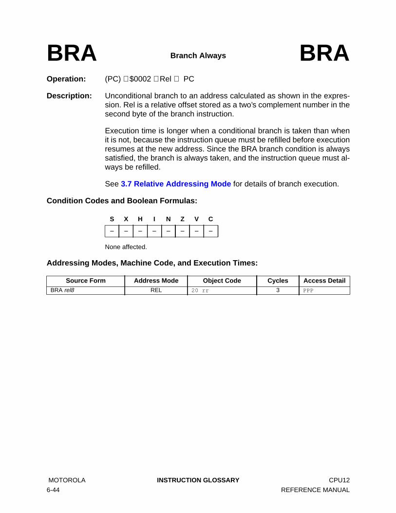
Operation: (PC) + $0002 + Rel ⇒ PC
Description: Unconditional branch to an address calculated as shown in the expres-sion. Rel is a relative offset stored as a two’s complement number in thesecond byte of the branch instruction.
Execution time is longer when a conditional branch is taken than whenit is not, because the instruction queue must be refilled before executionresumes at the new address. Since the BRA branch condition is alwayssatisfied, the branch is always taken, and the instruction queue must al-ways be refilled.
See 3.7 Relative Addressing Mode for details of branch execution.
Condition Codes and Boolean Formulas:
None affected.
Addressing Modes, Machine Code, and Execution Times:
BRA Branch Always BRA
S X H I N Z V C
– – – – – – – –
Source Form Address Mode Object Code Cycles Access DetailBRA rel8 REL 20 rr 3 PPP
MOTOROLA INSTRUCTION GLOSSARY CPU12
6-44 REFERENCE MANUAL

Operation: If (M) • (Mask) = 0, then branch
Description: Performs bitwise logical AND on memory location M and the mask sup-plied with the instruction, then branches if and only if all bits with a valueof one in the mask byte correspond to bits with a value of zero in the test-ed byte. Mask operands can be located at PC + 1, PC + 2, or PC + 4,depending on addressing mode. The branch offset is referenced to thenext address after the relative offset (rr) which is the last byte of the in-struction object code.
See 3.7 Relative Addressing Mode for details of branch execution.
Condition Codes and Boolean Formulas:
None affected.
Addressing Modes, Machine Code, and Execution Times:
BRCLR Branch if Bits Cleared BRCLR
S X H I N Z V C
– – – – – – – –
Source Form Address Mode 1
Notes:1. Indirect forms of indexed addressing cannot be used with this instruction.
Object Code CyclesAccessDetail
BRCLR opr8a, msk8, rel8BRCLR opr16a, msk8, rel8BRCLR oprx0_xysp, msk8, rel8BRCLR oprx9,xysp, msk8, rel8BRCLR oprx16,xysp, msk8, rel8
DIREXTIDXIDX1IDX2
4F dd mm rr
1F hh ll mm rr
0F xb mm rr
0F xb ff mm rr
0F xb ee ff mmrr
45468
rPPP
rfPPP
rPPP
rffPPP
frPffPPP
CPU12 INSTRUCTION GLOSSARY MOTOROLA
REFERENCE MANUAL 6-45

Operation: (PC) + $0002 ⇒ PC
Description: Never branches. BRN is effectively a 2-byte NOP that requires one cycleto execute. BRN is included in the instruction set to provide a comple-ment to the BRA instruction. The instruction is useful during program de-bug, to negate the effect of another branch instruction without disturbingthe offset byte. A complement for BRA is also useful in compiler imple-mentations.
Execution time is longer when a conditional branch is taken than whenit is not, because the instruction queue must be refilled before executionresumes at the new address. Since the BRN branch condition is neversatisfied, the branch is never taken, and only a single program fetch isneeded to update the instruction queue.
See 3.7 Relative Addressing Mode for details of branch execution.
Condition Codes and Boolean Formulas:
None affected.
Addressing Modes, Machine Code, and Execution Times:
BRN Branch Never BRN
S X H I N Z V C
– – – – – – – –
Source Form Address Mode Object Code Cycles Access DetailBRN rel8 REL 21 rr 1 P
MOTOROLA INSTRUCTION GLOSSARY CPU12
6-46 REFERENCE MANUAL
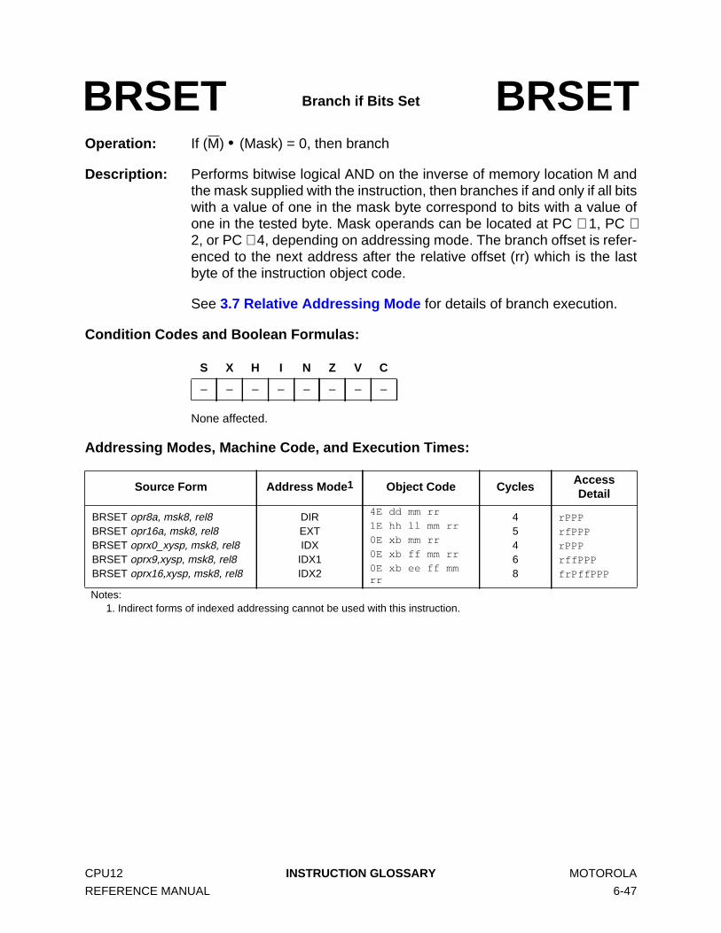
Operation: If (M) • (Mask) = 0, then branch
Description: Performs bitwise logical AND on the inverse of memory location M andthe mask supplied with the instruction, then branches if and only if all bitswith a value of one in the mask byte correspond to bits with a value ofone in the tested byte. Mask operands can be located at PC + 1, PC +2, or PC + 4, depending on addressing mode. The branch offset is refer-enced to the next address after the relative offset (rr) which is the lastbyte of the instruction object code.
See 3.7 Relative Addressing Mode for details of branch execution.
Condition Codes and Boolean Formulas:
None affected.
Addressing Modes, Machine Code, and Execution Times:
BRSET Branch if Bits Set BRSET
S X H I N Z V C
– – – – – – – –
Source Form Address Mode 1
Notes:1. Indirect forms of indexed addressing cannot be used with this instruction.
Object Code CyclesAccessDetail
BRSET opr8a, msk8, rel8BRSET opr16a, msk8, rel8BRSET oprx0_xysp, msk8, rel8BRSET oprx9,xysp, msk8, rel8BRSET oprx16,xysp, msk8, rel8
DIREXTIDXIDX1IDX2
4E dd mm rr
1E hh ll mm rr
0E xb mm rr
0E xb ff mm rr
0E xb ee ff mmrr
45468
rPPP
rfPPP
rPPP
rffPPP
frPffPPP
CPU12 INSTRUCTION GLOSSARY MOTOROLA
REFERENCE MANUAL 6-47

Operation: (M) + (Mask) ⇒ M
Description: Sets bits in memory location M. To set a bit, set the corresponding bit inthe mask byte. All other bits in M are unchanged. The mask byte can belocated at PC + 2, PC + 3, or PC + 4, depending upon addressing mode.
Condition Codes and Boolean Formulas:
Addressing Modes, Machine Code, and Execution Times:
BSET Set Bit(s) in Memory BSET
S X H I N Z V C
– – – – ∆ ∆ 0 –
N: Set if MSB of result is set; cleared otherwise.
Z: Set if result is $00; cleared otherwise.
V: 0; Cleared.
Source Form Address Mode 1
Notes:1. Indirect forms of indexed addressing cannot be used with this instruction.
Object Code Cycles Access DetailBSET opr8a, msk8BSET opr16a, msk8BSET oprx0_xysp, msk8BSET oprx9,xysp, msk8BSET oprx16,xysp, msk8
DIREXTIDXIDX1IDX2
4C dd mm
1C hh ll mm
0C xb mm
0C xb ff mm
0C xb ee ff mm
44446
rPOw
rPPw
rPOw
rPwP
frPwOP
MOTOROLA INSTRUCTION GLOSSARY CPU12
6-48 REFERENCE MANUAL

Operation: (SP) – $0002 ⇒ SPRTNH : RTNL ⇒ M(SP) : M(SP + 1)(PC) + Rel ⇒ PC
Description: Sets up conditions to return to normal program flow, then transfers con-trol to a subroutine. Uses the address of the instruction after the BSR asa return address.
Decrements the SP by two, to allow the two bytes of the return ad-dress to be stacked.
Stacks the return address (the SP points to the high order byte of thereturn address).
Branches to a location determined by the branch offset.
Subroutines are normally terminated with an RTS instruction, which re-stores the return address from the stack.
Condition Codes and Boolean Formulas:
None affected.
Addressing Modes, Machine Code, and Execution Times:
BSR Branch to Subroutine BSR
S X H I N Z V C
– – – – – – – –
Source Form Address Mode Object Code Cycles Access DetailBSR rel8 REL 07 rr 4 PPPS
CPU12 INSTRUCTION GLOSSARY MOTOROLA
REFERENCE MANUAL 6-49

Operation: If V = 0, then (PC) + $0002 + Rel ⇒ PC
Simple branch
Description: Tests the V status bit and branches if V = 0.
BVC causes a branch when a previous operation on two’s complementbinary values does not cause an overflow. That is, when BVC follows atwo’s complement operation, a branch occurs when the result of the op-eration is valid.
See 3.7 Relative Addressing Mode for details of branch execution.
Condition Codes and Boolean Formulas:
None affected.
Addressing Modes, Machine Code, and Execution Times:
BVC Branch if Overflow Cleared BVC
S X H I N Z V C
– – – – – – – –
Source Form Address Mode Object Code Cycles Access DetailBVC rel8 REL 28 rr 3/1 PPP/P1
Notes:1. PPP/P indicates this instruction takes three cycles to refill the instruction queue if the branch is taken and one
program fetch cycle if the branch is not taken.
Branch Complementary BranchTest Mnemonic Opcode Boolean Test Mnemonic Opcode Commentr>m BGT 2E Z + (N ⊕ V) = 0 r≤m BLE 2F Signedr≥m BGE 2C N ⊕ V = 0 r<m BLT 2D Signedr=m BEQ 27 Z = 1 r≠m BNE 26 Signedr≤m BLE 2F Z + (N ⊕ V) = 1 r>m BGT 2E Signedr<m BLT 2D N ⊕ V = 1 r≥m BGE 2C Signedr>m BHI 22 C + Z = 0 r≤m BLS 23 Unsignedr≥m BHS/BCC 24 C = 0 r<m BLO/BCS 25 Unsignedr=m BEQ 27 Z = 1 r≠m BNE 26 Unsignedr≤m BLS 23 C + Z = 1 r>m BHI 22 Unsignedr<m BLO/BCS 25 C = 1 r≥m BHS/BCC 24 Unsigned
Carry BCS 25 C = 1 No Carry BCC 24 SimpleNegative BMI 2B N = 1 Plus BPL 2A SimpleOverflow BVS 29 V = 1 No Overflow BVC 28 Simple
r=0 BEQ 27 Z = 1 r≠0 BNE 26 SimpleAlways BRA 20 — Never BRN 21 Unconditional
MOTOROLA INSTRUCTION GLOSSARY CPU12
6-50 REFERENCE MANUAL

Operation: If V = 1, then (PC) + $0002 + Rel ⇒ PC
Simple branch
Description: Tests the V status bit and branches if V = 1.
BVS causes a branch when a previous operation on two’s complementbinary values causes an overflow. That is, when BVS follows a two’scomplement operation, a branch occurs when the result of the operationis invalid.
See 3.7 Relative Addressing Mode for details of branch execution.
Condition Codes and Boolean Formulas:
None affected.
Addressing Modes, Machine Code, and Execution Times:
BVS Branch if Overflow Set BVS
S X H I N Z V C
– – – – – – – –
Source Form Address Mode Object Code Cycles Access DetailBVS rel8 REL 29 rr 3/1 PPP/P1
Notes:1. PPP/P indicates this instruction takes three cycles to refill the instruction queue if the branch is taken and one
program fetch cycle if the branch is not taken.
Branch Complementary BranchTest Mnemonic Opcode Boolean Test Mnemonic Opcode Commentr>m BGT 2E Z + (N ⊕ V) = 0 r≤m BLE 2F Signedr≥m BGE 2C N ⊕ V = 0 r<m BLT 2D Signedr=m BEQ 27 Z = 1 r≠m BNE 26 Signedr≤m BLE 2F Z + (N ⊕ V) = 1 r>m BGT 2E Signedr<m BLT 2D N ⊕ V = 1 r≥m BGE 2C Signedr>m BHI 22 C + Z = 0 r≤m BLS 23 Unsignedr≥m BHS/BCC 24 C = 0 r<m BLO/BCS 25 Unsignedr=m BEQ 27 Z = 1 r≠m BNE 26 Unsignedr≤m BLS 23 C + Z = 1 r>m BHI 22 Unsignedr<m BLO/BCS 25 C = 1 r≥m BHS/BCC 24 Unsigned
Carry BCS 25 C = 1 No Carry BCC 24 SimpleNegative BMI 2B N = 1 Plus BPL 2A SimpleOverflow BVS 29 V = 1 No Overflow BVC 28 Simple
r=0 BEQ 27 Z = 1 r≠0 BNE 26 SimpleAlways BRA 20 — Never BRN 21 Unconditional
CPU12 INSTRUCTION GLOSSARY MOTOROLA
REFERENCE MANUAL 6-51

Operation: (SP) – $0002 ⇒ SPRTNH : RTNL ⇒ M(SP) : M(SP + 1)(SP) – $0001 ⇒ SP(PPAGE) ⇒ M(SP)page ⇒ PPAGESubroutine Address ⇒ PC
Description: Sets up conditions to return to normal program flow, then transfers con-trol to a subroutine in expanded memory. Uses the address of the in-struction following the CALL as a return address. For code compatibility,CALL also executes correctly in devices that do not have expandedmemory capability.
Decrements the SP by two, to allow the two bytes of the return ad-dress to be stacked.
Stacks the return address (the SP points to the high order byte of thereturn address).
Decrements the SP by one, to allow the current memory page valuein the PPAGE register to be stacked.
Stacks the content of PPAGE.
Writes a new page value supplied by the instruction to PPAGE.
Transfers control to the subroutine.
In indexed-indirect modes, the subroutine address and the PPAGEvalue are fetched from memory in the order M high byte, M low byte, andnew PPAGE value.
Expanded-memory subroutines must be terminated by an RTC instruc-tion, which restores the return address and PPAGE value from the stack.
Condition Codes and Boolean Formulas:
None affected.
Addressing Modes, Machine Code, and Execution Times:
CALL Call Subroutine in Expanded Memory CALL
S X H I N Z V C
– – – – – – – –
Source Form Address Mode Object Code Cycles Access DetailCALL opr16a, pageCALL oprx0_xysp, pageCALL oprx9,xysp, pageCALL oprx16,xysp, pageCALL [D,xysp]CALL [oprx16,xysp]
EXTIDXIDX1IDX2
[D,IDX][IDX2]
4A hh ll pg
4B xb pg
4B xb ff pg
4B xb ee ff pg
4B xb
4B xb ee ff
8889
1010
gnfSsPPP
gnfSsPPP
gnfSsPPP
fgnfSsPPP
fIignSsPPP
fIignSsPPP
MOTOROLA INSTRUCTION GLOSSARY CPU12
6-52 REFERENCE MANUAL

Operation: (A) – (B)
Description: Compares the content of accumulator A to the content of accumulator Band sets the condition codes, which may then be used for arithmetic andlogical conditional branches. The contents of the accumulators are notchanged.
Condition Codes and Boolean Formulas:
Addressing Modes, Machine Code, and Execution Times:
CBA Compare Accumulators CBA
S X H I N Z V C
– – – – ∆ ∆ ∆ ∆
N: Set if MSB of result is set; cleared otherwise.
Z: Set if result is $00; cleared otherwise.
V: A7 • B7 • R7 + A7 • B7 • R7Set if a two’s complement overflow resulted from the operation; clearedotherwise.
C: A7 • B7 + B7 • R7 + R7 + A7Set if there was a borrow from the MSB of the result; cleared otherwise.
Source Form Address Mode Object Code Cycles Access DetailCBA INH 18 17 2 OO
CPU12 INSTRUCTION GLOSSARY MOTOROLA
REFERENCE MANUAL 6-53

Operation: 0 ⇒ C bit
Description: Clears the C status bit. This instruction is assembled as ANDCC #$FE.The ANDCC instruction can be used to clear any combination of bits inthe CCR in one operation.
CLC can be used to set up the C bit prior to a shift or rotate instructioninvolving the C bit.
Condition Codes and Boolean Formulas:
Addressing Modes, Machine Code, and Execution Times:
CLC Clear Carry CLC
S X H I N Z V C
– – – – – – – 0
C: 0; Cleared.
Source Form Address Mode Object Code Cycles Access DetailCLC translates to...ANDCC #$FE
IMM 10 FE 1 P
MOTOROLA INSTRUCTION GLOSSARY CPU12
6-54 REFERENCE MANUAL

Operation: 0 ⇒ I bit
Description: Clears the I mask bit. This instruction is assembled as ANDCC #$EF.The ANDCC instruction can be used to clear any combination of bits inthe CCR in one operation.
When the I bit is cleared, interrupts are enabled. There is a one cycle(bus clock) delay in the clearing mechanism for the I bit so that, if inter-rupts were previously disabled, the next instruction after a CLI willalways be executed, even if there was an interrupt pending prior to exe-cution of the CLI instruction.
Condition Codes and Boolean Formulas:
Addressing Modes, Machine Code, and Execution Times:
CLI Clear Interrupt Mask CLI
S X H I N Z V C
– – – 0 – – – –
I: 0; Cleared.
Source Form Address Mode Object Code Cycles Access DetailCLI translates to...ANDCC #$EF
IMM 10 EF 1 P
CPU12 INSTRUCTION GLOSSARY MOTOROLA
REFERENCE MANUAL 6-55

Operation: 0 ⇒ M
Description: All bits in memory location M are cleared to zero.
Condition Codes and Boolean Formulas:
Addressing Modes, Machine Code, and Execution Times:
CLR Clear Memory CLR
S X H I N Z V C
– – – – 0 1 0 0
N: 0; Cleared.
Z: 1; Set.
V: 0; Cleared.
C: 0; Cleared.
Source Form Address Mode Object Code Cycles Access DetailCLR opr16aCLR oprx0_xyspCLR oprx9,xyspCLR oprx16,xyspCLR [D,xysp]CLR [oprx16,xysp]
EXTIDXIDX1IDX2
[D,IDX][IDX2]
79 hh ll
69 xb
69 xb ff
69 xb ee ff
69 xb
69 xb ee ff
323355
wOP
Pw
PwO
PwP
PIfPw
PIPPw
MOTOROLA INSTRUCTION GLOSSARY CPU12
6-56 REFERENCE MANUAL
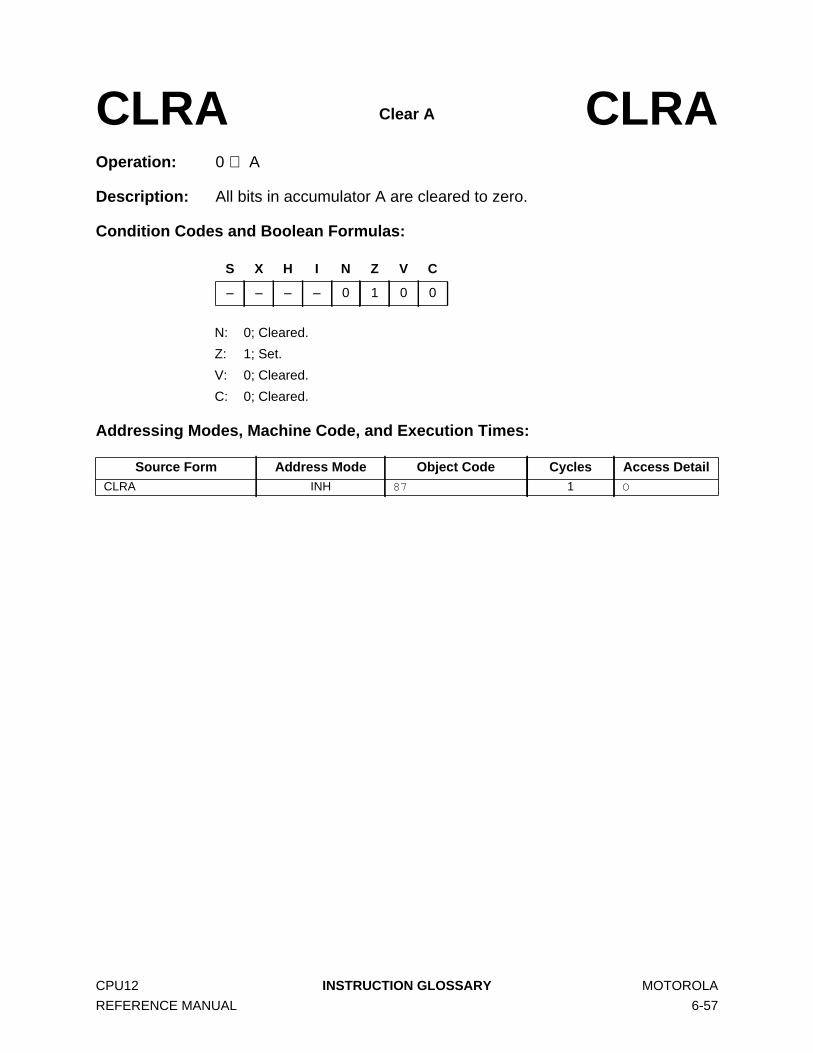
Operation: 0 ⇒ A
Description: All bits in accumulator A are cleared to zero.
Condition Codes and Boolean Formulas:
Addressing Modes, Machine Code, and Execution Times:
CLRA Clear A CLRA
S X H I N Z V C
– – – – 0 1 0 0
N: 0; Cleared.
Z: 1; Set.
V: 0; Cleared.
C: 0; Cleared.
Source Form Address Mode Object Code Cycles Access DetailCLRA INH 87 1 O
CPU12 INSTRUCTION GLOSSARY MOTOROLA
REFERENCE MANUAL 6-57
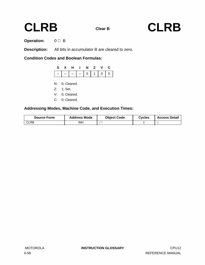
Operation: 0 ⇒ B
Description: All bits in accumulator B are cleared to zero.
Condition Codes and Boolean Formulas:
Addressing Modes, Machine Code, and Execution Times:
CLRB Clear B CLRB
S X H I N Z V C
– – – – 0 1 0 0
N: 0; Cleared.
Z: 1; Set.
V: 0; Cleared.
C: 0; Cleared.
Source Form Address Mode Object Code Cycles Access DetailCLRB INH C7 1 O
MOTOROLA INSTRUCTION GLOSSARY CPU12
6-58 REFERENCE MANUAL

Operation: 0 ⇒ V bit
Description: Clears the V status bit. This instruction is assembled as ANDCC #$FD.The ANDCC instruction can be used to clear any combination of bits inthe CCR in one operation.
Condition Codes and Boolean Formulas:
Addressing Modes, Machine Code, and Execution Times:
CLV Clear Two’s Complement Overflow Bit CLV
S X H I N Z V C
– – – – – – 0 –
V: 0; Cleared.
Source Form Address Mode Object Code Cycles Access DetailCLV translates to...ANDCC #$FD IMM 10 FD 1 P
CPU12 INSTRUCTION GLOSSARY MOTOROLA
REFERENCE MANUAL 6-59

Operation: (A) – (M)
Description: Compares the content of accumulator A to the content of memory loca-tion M and sets the condition codes, which may then be used for arith-metic and logical conditional branching. The contents of A and locationM are not changed.
Condition Codes and Boolean Formulas:
Addressing Modes, Machine Code, and Execution Times:
CMPA Compare A CMPA
S X H I N Z V C
– – – – ∆ ∆ ∆ ∆
N: Set if MSB of result is set; cleared otherwise.
Z: Set if result is $00; cleared otherwise.
V: X7 • M7 • R7 + X7 • M7 • R7Set if a two’s complement overflow resulted from the operation; clearedotherwise.
C: X7 • M7 + M7 • R7 + R7 + X7Set if there was a borrow from the MSB of the result; cleared otherwise.
Source Form Address Mode Object Code Cycles Access DetailCMPA #opr8iCMPA opr8aCMPA opr16aCMPA oprx0_xyspCMPA oprx9,xyspCMPA oprx16,xyspCMPA [D,xysp]CMPA [oprx16,xysp]
IMMDIREXTIDXIDX1IDX2
[D,IDX][IDX2]
81 ii
91 dd
B1 hh ll
A1 xb
A1 xb ff
A1 xb ee ff
A1 xb
A1 xb ee ff
13333466
P
rfP
rOP
rfP
rPO
frPP
fIfrfP
fIPrfP
MOTOROLA INSTRUCTION GLOSSARY CPU12
6-60 REFERENCE MANUAL

Operation: (B) – (M)
Description: Compares the content of accumulator B to the content of memory loca-tion M and sets the condition codes, which may then be used for arith-metic and logical conditional branching. The contents of B and locationM are not changed.
Condition Codes and Boolean Formulas:
Addressing Modes, Machine Code, and Execution Times:
CMPB Compare B CMPB
S X H I N Z V C
– – – – ∆ ∆ ∆ ∆
N: Set if MSB of result is set; cleared otherwise.
Z: Set if result is $00; cleared otherwise.
V: X7 • M7 • R7 + X7 • M7 • R7Set if a two’s complement overflow resulted from the operation; clearedotherwise.
C: X7 • M7 + M7 • R7 + R7 + X7Set if there was a borrow from the MSB of the result; cleared otherwise.
Source Form Address Mode Object Code Cycles Access DetailCMPB #opr8iCMPB opr8aCMPB opr16aCMPB oprx0_xyspCMPB oprx9,xyspCMPB oprx16,xyspCMPB [D,xysp]CMPB [oprx16,xysp]
IMMDIREXTIDXIDX1IDX2
[D,IDX][IDX2]
C1 ii
D1 dd
F1 hh ll
E1 xb
E1 xb ff
E1 xb ee ff
E1 xb
E1 xb ee ff
13333466
P
rfP
rOP
rfP
rPO
frPP
fIfrfP
fIPrfP
CPU12 INSTRUCTION GLOSSARY MOTOROLA
REFERENCE MANUAL 6-61

Operation: (M) = $FF – (M) ⇒ M
Description: Replaces the content of memory location M with its one’s complement.Each bit of M is complemented. Immediately after a COM operation onunsigned values, only the BEQ, BNE, LBEQ, and LBNE branches canbe expected to perform consistently. After operation on two’s comple-ment values, all signed branches are available.
Condition Codes and Boolean Formulas:
Addressing Modes, Machine Code, and Execution Times:
COM Complement Memory COM
S X H I N Z V C
– – – – ∆ ∆ 0 1
N: Set if MSB of result is set; cleared otherwise.
Z: Set if result is $00; cleared otherwise.
V: 0; Cleared.
C: 1; Set (for M6800 compatibility).
Source Form Address Mode Object Code Cycles Access DetailCOM opr16aCOM oprx0_xyspCOM oprx9,xyspCOM oprx16,xyspCOM [D,xysp]COM [oprx16,xysp]
EXTIDXIDX1IDX2
[D,IDX][IDX2]
71 hh ll
61 xb
61 xb ff
61 xb ee ff
61 xb
61 xb ee ff
434566
rOPw
rPw
rPOw
frPPw
fIfrPw
fIPrPw
MOTOROLA INSTRUCTION GLOSSARY CPU12
6-62 REFERENCE MANUAL

Operation: (A) = $FF – (A) ⇒ A
Description: Replaces the content of accumulator A with its one’s complement. Eachbit of A is complemented. Immediately after a COM operation on un-signed values, only the BEQ, BNE, LBEQ, and LBNE branches can beexpected to perform consistently. After operation on two’s complementvalues, all signed branches are available.
Condition Codes and Boolean Formulas:
Addressing Modes, Machine Code, and Execution Times:
COMA Complement A COMA
S X H I N Z V C
– – – – ∆ ∆ 0 1
N: Set if MSB of result is set; cleared otherwise.
Z: Set if result is $00; cleared otherwise.
V: 0; Cleared.
C: 1; Set (for M6800 compatibility).
Source Form Address Mode Object Code Cycles Access DetailCOMA INH 41 1 O
CPU12 INSTRUCTION GLOSSARY MOTOROLA
REFERENCE MANUAL 6-63

Operation: (B) = $FF – (B) ⇒ B
Description: Replaces the content of accumulator B with its one’s complement. Eachbit of B is complemented. Immediately after a COM operation on un-signed values, only the BEQ, BNE, LBEQ, and LBNE branches can beexpected to perform consistently. After operation on two’s complementvalues, all signed branches are available.
Condition Codes and Boolean Formulas:
Addressing Modes, Machine Code, and Execution Times:
COMB Complement B COMB
S X H I N Z V C
– – – – ∆ ∆ 0 1
N: Set if MSB of result is set; cleared otherwise.
Z: Set if result is $00; cleared otherwise.
V: 0; Cleared.
C: 1; Set (for M6800 compatibility).
Source Form Address Mode Object Code Cycles Access DetailCOMB INH 51 1 O
MOTOROLA INSTRUCTION GLOSSARY CPU12
6-64 REFERENCE MANUAL

Operation: (A : B) – (M : M + 1)
Description: Compares the content of double accumulator D with a 16-bit value at theaddress specified, and sets the condition codes accordingly. The com-pare is accomplished internally by a 16-bit subtract of (M : M + 1) from Dwithout modifying either D or (M : M + 1).
Condition Codes and Boolean Formulas:
Addressing Modes, Machine Code, and Execution Times:
CPD Compare Double Accumulator CPD
S X H I N Z V C
– – – – ∆ ∆ ∆ ∆
N: Set if MSB of result is set; cleared otherwise.
Z: Set if result is $0000; cleared otherwise.
V: D15 • M15 • R15 + D15 • M15 • R15Set if two’s complement overflow resulted from the operation; clearedotherwise.
C: D15 • M15 + M15 • R15 + R15 + D15Set if the absolute value of the content of memory is larger than theabsolute value of the accumulator; cleared otherwise.
Source Form Address Mode Object Code Cycles Access DetailCPD #opr16iCPD opr8aCPD opr16aCPD oprx0_xyspCPD oprx9,xyspCPD oprx16,xyspCPD [D,xysp]CPD [oprx16,xysp]
IMMDIREXTIDXIDX1IDX2
[D,IDX][IDX2]
8C jj kk
9C dd
BC hh ll
AC xb
AC xb ff
AC xb ee ff
AC xb
AC xb ee ff
23333466
OP
RfP
ROP
RfP
RPO
fRPP
fIfRfP
fIPRfP
CPU12 INSTRUCTION GLOSSARY MOTOROLA
REFERENCE MANUAL 6-65

Operation: (SP) – (M : M + 1)
Description: Compares the content of the SP with a 16-bit value at the address spec-ified, and sets the condition codes accordingly. The compare is accom-plished internally by doing a 16-bit subtract of (M : M + 1) from the SPwithout modifying either the SP or (M : M + 1).
Condition Codes and Boolean Formulas:
Addressing Modes, Machine Code, and Execution Times:
CPS Compare Stack Pointer CPS
S X H I N Z V C
– – – – ∆ ∆ ∆ ∆
N: Set if MSB of result is set; cleared otherwise.
Z: Set if result is $0000; cleared otherwise.
V: S15 • M15 • R15 + S15 • M15 • R15Set if two’s complement overflow resulted from the operation; clearedotherwise.
C: S15 • M15 + M15 • R15 + R15 + S15Set if the absolute value of the content of memory is larger than theabsolute value of the SP; cleared otherwise.
Source Form Address Mode Object Code Cycles Access DetailCPS #opr16iCPS opr8aCPS opr16aCPS oprx0_xyspCPS oprx9,xyspCPS oprx16,xyspCPS [D,xysp]CPS [oprx16,xysp]
IMMDIREXTIDXIDX1IDX2
[D,IDX][IDX2]
8F jj kk
9F dd
BF hh ll
AF xb
AF xb ff
AF xb ee ff
AF xb
AF xb ee ff
23333466
OP
RfP
ROP
RfP
RPO
fRPP
fIfRfP
fIPRfP
MOTOROLA INSTRUCTION GLOSSARY CPU12
6-66 REFERENCE MANUAL

Operation: (X) – (M : M + 1)
Description: Compares the content of index register X with a 16-bit value at the ad-dress specified, and sets the condition codes accordingly. The compareis accomplished internally by a 16-bit subtract of (M : M + 1) from indexregister X without modifying either index register X or (M : M + 1).
Condition Codes and Boolean Formulas:
Addressing Modes, Machine Code, and Execution Times:
CPX Compare Index Register X CPX
S X H I N Z V C
– – – – ∆ ∆ ∆ ∆
N: Set if MSB of result is set; cleared otherwise.
Z: Set if result is $0000; cleared otherwise.
V: X15 • M15 • R15 + X15 • M15 • R15Set if two’s complement overflow resulted from the operation; clearedotherwise.
C: X15 • M15 + M15 • R15 + R15 + X15Set if the absolute value of the content of memory is larger than theabsolute value of the index register; cleared otherwise.
Source Form Address Mode Object Code Cycles Access DetailCPX #opr16iCPX opr8aCPX opr16aCPX oprx0_xyspCPX oprx9,xyspCPX oprx16,xyspCPX [D,xysp]CPX [oprx16,xysp]
IMMDIREXTIDXIDX1IDX2
[D,IDX][IDX2]
8E jj kk
9E dd
BE hh ll
AE xb
AE xb ff
AE xb ee ff
AE xb
AE xb ee ff
23333466
OP
RfP
ROP
RfP
RPO
fRPP
fIfRfP
fIPRfP
CPU12 INSTRUCTION GLOSSARY MOTOROLA
REFERENCE MANUAL 6-67

Operation: (Y) – (M : M + 1)
Description: Compares the content of index register Y to a 16-bit value at the addressspecified, and sets the condition codes accordingly. The compare is ac-complished internally by a 16-bit subtract of (M : M + 1) from Y withoutmodifying either Y or (M : M + 1).
Condition Codes and Boolean Formulas:
Addressing Modes, Machine Code, and Execution Times:
CPY Compare Index Register Y CPY
S X H I N Z V C
– – – – ∆ ∆ ∆ ∆
N: Set if MSB of result is set; cleared otherwise.
Z: Set if result is $0000; cleared otherwise.
V: Y15 • M15 • R15 + Y15 • M15 • R15Set if two’s complement overflow resulted from the operation; clearedotherwise.
C: Y15 • M15 + M15 • R15 + R15 + Y15Set if the absolute value of the content of memory is larger than theabsolute value of the index register; cleared otherwise.
Source Form Address Mode Object Code Cycles Access DetailCPY #opr16iCPY opr8aCPY opr16aCPY oprx0_xyspCPY oprx9,xyspCPY oprx16,xyspCPY [D,xysp]CPY [oprx16,xysp]
IMMDIREXTIDXIDX1IDX2
[D,IDX][IDX2]
8D jj kk
9D dd
BD hh ll
AD xb
AD xb ff
AD xb ee ff
AD xb
AD xb ee ff
23333466
OP
RfP
ROP
RfP
RPO
fRPP
fIfRfP
fIPRfP
MOTOROLA INSTRUCTION GLOSSARY CPU12
6-68 REFERENCE MANUAL

Description: DAA adjusts the content of accumulator A and the state of the C statusbit to represent the correct binary-coded-decimal sum and the associat-ed carry when a BCD calculation has been performed. In order to exe-cute DAA, the content of accumulator A, the state of the C status bit, andthe state of the H status bit must all be the result of performing an ABA,ADD or ADC on BCD operands, with or without an initial carry.
The table below shows DAA operation for all legal combinations of inputoperands. Columns 1 through 4 represent the results of ABA, ADC, orADD operations on BCD operands. The correction factor in column 5 isadded to the accumulator to restore the result of an operation on twoBCD operands to a valid BCD value, and to set or clear the C bit. All val-ues are in hexadecimal.
Condition Codes and Boolean Formulas:
Addressing Modes, Machine Code, and Execution Times:
DAA Decimal Adjust A DAA
1 2 3 4 5 6
InitialC Bit Value
Value ofA[7:4]
InitialH Bit Value
Value ofA[3:0]
CorrectionFactor
CorrectedC Bit Value
0 0–9 0 0–9 00 0
0 0–8 0 A–F 06 0
0 0–9 1 0–3 06 0
0 A–F 0 0–9 60 1
0 9–F 0 A–F 66 1
0 A–F 1 0–3 66 1
1 0–2 0 0–9 60 1
1 0–2 0 A–F 66 1
1 0–3 1 0–3 66 1
S X H I N Z V C
– – – – ∆ ∆ ? ∆
N: Set if MSB of result is set; cleared otherwise.
Z: Set if result is $00; cleared otherwise.
V: Undefined.
C: Represents BCD carry. See table above.
Source Form Address Mode Object Code Cycles Access DetailDAA INH 18 07 3 OfO
CPU12 INSTRUCTION GLOSSARY MOTOROLA
REFERENCE MANUAL 6-69

Operation: (Counter) – 1 ⇒ CounterIf (Counter) = 0, then (PC) + $0003 + Rel ⇒ PC,
Description: Subtract one from the specified counter register A, B, D, X, Y, or SP. Ifthe counter register has reached zero, execute a branch to the specifiedrelative destination. The DBEQ instruction is encoded into three bytes ofmachine code including the 9-bit relative offset (–256 to +255 locationsfrom the start of the next instruction).
IBEQ and TBEQ instructions are similar to DBEQ except that the counteris incremented or tested rather than being decremented. Bits 7 and 6 ofthe instruction postbyte are used to determine which operation is to beperformed.
Condition Codes and Boolean Formulas:
None affected.
Addressing Modes, Machine Code, and Execution Times:
DBEQ Decrement and Branch if Equal to Zero DBEQ
S X H I N Z V C
– – – – – – – –
Source Form Address Mode Object Code 1
Notes:1. Encoding for lb is summarized in the following table. Bit 3 is not used (don’t care), bit 5 selects branch on zero
(DBEQ – 0) or not zero (DBNE – 1) versions, and bit 4 is the sign bit of the 9-bit relative offset. Bits 7 and 6 wouldbe 0:0 for DBEQ.
Cycles Access DetailDBEQ abdxys, rel9 REL 04 lb rr 3/3 PPP
CountRegister
Bits 2:0 Source FormObject Code
(if offset is positive)Object Code
(if offset is negative)
AB
000001
DBEQ A, rel9DBEQ B, rel9
04 00 rr
04 01 rr
04 10 rr
04 11 rr
DXY
SP
100101110111
DBEQ D, rel9DBEQ X, rel9DBEQ Y, rel9DBEQ SP, rel9
04 04 rr
04 05 rr
04 06 rr
04 07 rr
04 14 rr
04 15 rr
04 16 rr
04 17 rr
MOTOROLA INSTRUCTION GLOSSARY CPU12
6-70 REFERENCE MANUAL

Operation: (Counter) – 1 ⇒ CounterIf (Counter) not = 0, then (PC) + $0003 + Rel ⇒ PC,
Description: Subtract one from the specified counter register A, B, D, X, Y, or SP. Ifthe counter register has not been decremented to zero, execute abranch to the specified relative destination. The DBNE instruction is en-coded into three bytes of machine code including a 9-bit relative offset(–256 to +255 locations from the start of the next instruction).
IBNE and TBNE instructions are similar to DBNE except that the counteris incremented or tested rather than being decremented. Bits 7 and 6 ofthe instruction postbyte are used to determine which operation is to beperformed.
Condition Codes and Boolean Formulas:
None affected.
Addressing Modes, Machine Code, and Execution Times:
DBNE Decrement and Branch if Not Equal to Zero DBNE
S X H I N Z V C
– – – – – – – –
Source Form Address Mode Object Code 1
Notes:1. Encoding for lb is summarized in the following table. Bit 3 is not used (don’t care), bit 5 selects branch on zero
(DBEQ – 0) or not zero (DBNE – 1) versions, and bit 4 is the sign bit of the 9-bit relative offset. Bits 7 and 6 wouldbe 0:0 for DBNE.
Cycles Access DetailDBNE abdxys, rel9 REL 04 lb rr 3/3 PPP
CountRegister
Bits 2:0 Source FormObject Code
(if offset is positive)Object Code
(if offset is negative)
AB
000001
DBNE A, rel9DBNE B, rel9
04 20 rr
04 21 rr
04 30 rr
04 31 rr
DXY
SP
100101110111
DBNE D, rel9DBNE X, rel9DBNE Y, rel9DBNE SP, rel9
04 24 rr
04 25 rr
04 26 rr
04 27 rr
04 34 rr
04 35 rr
04 36 rr
04 37 rr
CPU12 INSTRUCTION GLOSSARY MOTOROLA
REFERENCE MANUAL 6-71
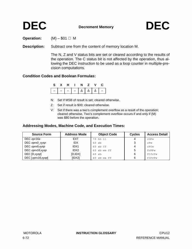
Operation: (M) – $01 ⇒ M
Description: Subtract one from the content of memory location M.
The N, Z and V status bits are set or cleared according to the results ofthe operation. The C status bit is not affected by the operation, thus al-lowing the DEC instruction to be used as a loop counter in multiple-pre-cision computations.
Condition Codes and Boolean Formulas:
Addressing Modes, Machine Code, and Execution Times:
DEC Decrement Memory DEC
S X H I N Z V C
– – – – ∆ ∆ ∆ –
N: Set if MSB of result is set; cleared otherwise.
Z: Set if result is $00; cleared otherwise.
V: Set if there was a two’s complement overflow as a result of the operation;cleared otherwise. Two’s complement overflow occurs if and only if (M)was $80 before the operation.
Source Form Address Mode Object Code Cycles Access DetailDEC opr16aDEC oprx0_xyspDEC oprx9,xyspDEC oprx16,xyspDEC [D,xysp]DEC [oprx16,xysp]
EXTIDXIDX1IDX2
[D,IDX][IDX2]
73 hh ll
63 xb
63 xb ff
63 xb ee ff
63 xb
63 xb ee ff
434566
rOPw
rPw
rPOw
frPPw
fIfrPw
fIPrPw
MOTOROLA INSTRUCTION GLOSSARY CPU12
6-72 REFERENCE MANUAL

Operation: (A) – $01 ⇒ A
Description: Subtract one from the content of accumulator A.
The N, Z and V status bits are set or cleared according to the results ofthe operation. The C status bit is not affected by the operation, thus al-lowing the DEC instruction to be used as a loop counter in multiple-pre-cision computations.
Condition Codes and Boolean Formulas:
Addressing Modes, Machine Code, and Execution Times:
DECA Decrement A DECA
S X H I N Z V C
– – – – ∆ ∆ ∆ –
N: Set if MSB of result is set; cleared otherwise.
Z: Set if result is $00; cleared otherwise.
V: Set if there was a two’s complement overflow as a result of the operation;cleared otherwise. Two’s complement overflow occurs if and only if (A) was$80 before the operation.
Source Form Address Mode Object Code Cycles Access DetailDECA INH 43 1 O
CPU12 INSTRUCTION GLOSSARY MOTOROLA
REFERENCE MANUAL 6-73
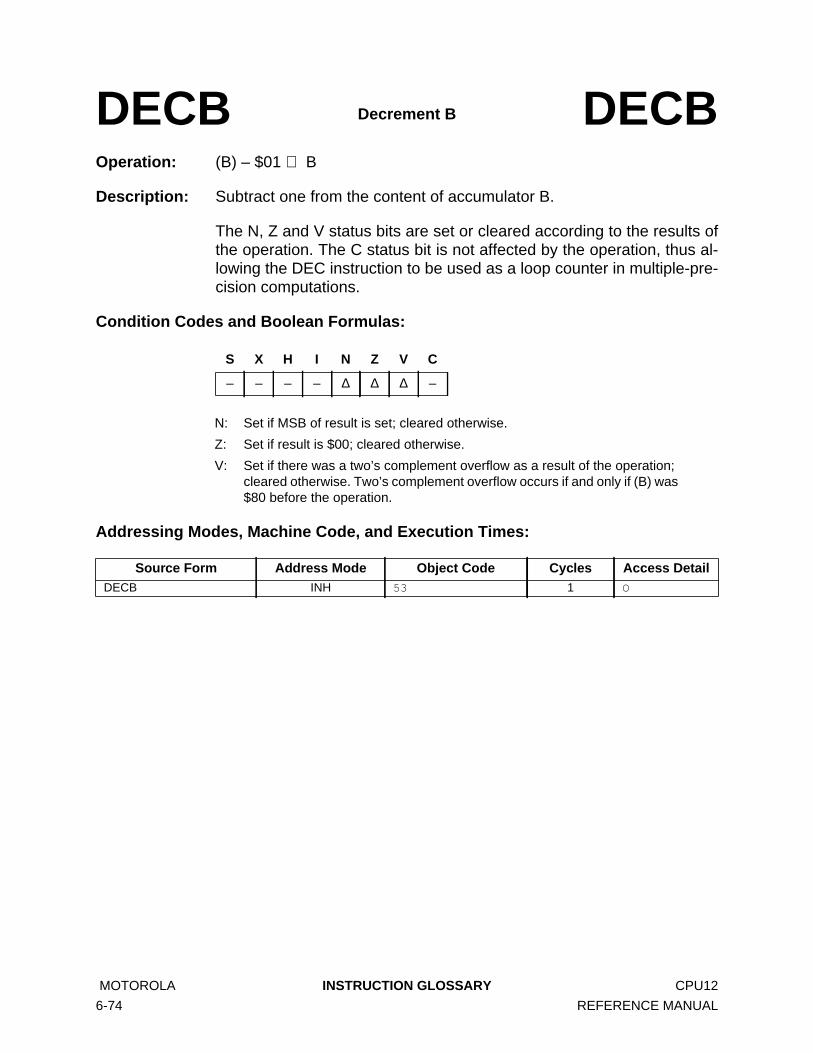
Operation: (B) – $01 ⇒ B
Description: Subtract one from the content of accumulator B.
The N, Z and V status bits are set or cleared according to the results ofthe operation. The C status bit is not affected by the operation, thus al-lowing the DEC instruction to be used as a loop counter in multiple-pre-cision computations.
Condition Codes and Boolean Formulas:
Addressing Modes, Machine Code, and Execution Times:
DECB Decrement B DECB
S X H I N Z V C
– – – – ∆ ∆ ∆ –
N: Set if MSB of result is set; cleared otherwise.
Z: Set if result is $00; cleared otherwise.
V: Set if there was a two’s complement overflow as a result of the operation;cleared otherwise. Two’s complement overflow occurs if and only if (B) was$80 before the operation.
Source Form Address Mode Object Code Cycles Access DetailDECB INH 53 1 O
MOTOROLA INSTRUCTION GLOSSARY CPU12
6-74 REFERENCE MANUAL

Operation: (SP) – $0001 ⇒ SP
Description: Subtract one from the SP. This instruction assembles to LEAS –1,SP.The LEAS instruction does not affect condition codes as DEX or DEY in-structions do.
Condition Codes and Boolean Formulas:
None affected.
Addressing Modes, Machine Code, and Execution Times:
DES Decrement Stack Pointer DES
S X H I N Z V C
– – – – – – – –
Source Form Address Mode Object Code Cycles Access DetailDES translates to...LEAS –1,SP
IDX 1B 9F 2 PP1
Notes:1. Due to internal CPU requirements, the program word fetch is performed twice to the same address during this
instruction.
CPU12 INSTRUCTION GLOSSARY MOTOROLA
REFERENCE MANUAL 6-75
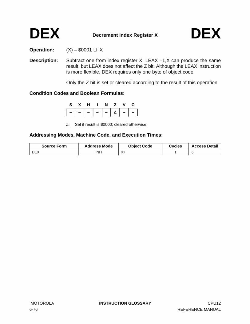
Operation: (X) – $0001 ⇒ X
Description: Subtract one from index register X. LEAX –1,X can produce the sameresult, but LEAX does not affect the Z bit. Although the LEAX instructionis more flexible, DEX requires only one byte of object code.
Only the Z bit is set or cleared according to the result of this operation.
Condition Codes and Boolean Formulas:
Addressing Modes, Machine Code, and Execution Times:
DEX Decrement Index Register X DEX
S X H I N Z V C
– – – – – ∆ – –
Z: Set if result is $0000; cleared otherwise.
Source Form Address Mode Object Code Cycles Access DetailDEX INH 09 1 O
MOTOROLA INSTRUCTION GLOSSARY CPU12
6-76 REFERENCE MANUAL

Operation: (Y) – $0001 ⇒ Y
Description: Subtract one from index register Y. LEAY –1,Y can produce the sameresult, but LEAY does not affect the Z bit. Although the LEAY instructionis more flexible, DEY requires only one byte of object code.
Only the Z bit is set or cleared according to the result of this operation.
Condition Codes and Boolean Formulas:
Addressing Modes, Machine Code, and Execution Times:
DEY Decrement Index Register Y DEY
S X H I N Z V C
– – – – – ∆ – –
Z: Set if result is $0000; cleared otherwise.
Source Form Address Mode Object Code Cycles Access DetailDEY INH 03 1 O
CPU12 INSTRUCTION GLOSSARY MOTOROLA
REFERENCE MANUAL 6-77

Operation: (Y : D) ÷ (X) ⇒ Y; Remainder ⇒ D
Description: Divides a 32-bit unsigned dividend by a 16-bit divisor, producing a 16-bitunsigned quotient and an unsigned 16-bit remainder. All operands andresults are located in CPU registers. If an attempt to divide by zero ismade, the contents of double accumulator D and index register Y do notchange, but the states of the N and Z bits in the CCR are undefined.
Condition Codes and Boolean Formulas:
Addressing Modes, Machine Code, and Execution Times:
EDIV Extended Divide 32-Bit by 16-Bit(Unsigned) EDIV
S X H I N Z V C
– – – – ∆ ∆ ∆ ∆
N: Set if MSB of result is set; cleared otherwise. Undefined after over-flow or division by zero.
Z: Set if result is $0000; cleared otherwise. Undefined after overflow ordivision by zero.
V: Set if the result was > $FFFF; cleared otherwise. Undefined after di-vision by zero.
C: Set if divisor was $0000; cleared otherwise.
Source Form Address Mode Object Code Cycles Access DetailEDIV INH 11 11 ffffffffffO
MOTOROLA INSTRUCTION GLOSSARY CPU12
6-78 REFERENCE MANUAL

Operation: (Y : D) ÷ (X) ⇒ Y; Remainder ⇒ D
Description: Divides a signed 32-bit dividend by a 16-bit signed divisor, producing asigned 16-bit quotient and a signed 16-bit remainder. All operands andresults are located in CPU registers. If an attempt to divide by zero ismade, the C status bit is set and the contents of double accumulator Dand index register Y do not change, but the states of the N and Z bits inthe CCR are undefined.
Condition Codes and Boolean Formulas:
Addressing Modes, Machine Code, and Execution Times:
EDIVS Extended Divide 32-Bit by 16-Bit(Signed) EDIVS
S X H I N Z V C
– – – – ∆ ∆ ∆ ∆
N: Set if MSB of result is set; cleared otherwise. Undefined after overflow ordivision by zero.
Z: Set if result is $0000; cleared otherwise. Undefined after overflow or divisionby zero.
V: Set if the result was > $7FFF or < $8000; cleared otherwise. Undefined afterdivision by zero.
C: Set if divisor was $0000; cleared otherwise. (Indicates division by zero.)
Source Form Address Mode Object Code Cycles Access DetailEDIVS INH 18 14 12 OffffffffffO
CPU12 INSTRUCTION GLOSSARY MOTOROLA
REFERENCE MANUAL 6-79

E
Operation: (M(X) : M(X+1)) × (M(Y) : M(Y+1)) + (M ~ M+3) ⇒ M ~ M+3Description: A 16-bit value is multiplied by a 16-bit value to produce a 32-bit interme-diate result. This 32-bit intermediate result is then added to the contentof a 32-bit accumulator in memory. EMACS is a signed integer opera-tion. All operands and results are located in memory. When the EMACSinstruction is executed, the first source operand is fetched from an ad-dress pointed to by X, and the second source operand is fetched froman address pointed to by index register Y. Before the instruction is exe-cuted, the X and Y index registers must contain values that point to themost significant bytes of the source operands. The most significant byteof the 32-bit result is specified by an extended address supplied with theinstruction.
Condition Codes and Boolean Formulas:
Addressing Modes, Machine Code, and Execution Times:
MACS Extended Multiply and Accumulate(Signed)
16-Bit by 16-Bit to 32-BitEMACS
S X H I N Z V C
– – – – ∆ ∆ ∆ ∆
N: Set if MSB of result is set; cleared otherwise.
Z: Set if result is $00000000; cleared otherwise.
V: M31 • I31 • R31 + M31 • I31 • R31Set if result > $7FFFFFFF (+ overflow) or < $80000000 (– underflow).Indicates two’s complement overflow.
C: M15 • I15 + I15 • R15 + R15 • M15Set if there was a carry from bit 15 of the result; cleared otherwise.Indicates a carry from low word to high word of the result occurred.
Source Form 1
Notes:1. opr16a is an extended address specification. Both X and Y point to source operands.
Address Mode Object Code Cycles Access DetailEMACS opr16a Special 18 12 hh ll 13 ORROfffRRfWWP
MOTOROLA INSTRUCTION GLOSSARY CPU12
6-80 REFERENCE MANUAL

Operation: MAX ((D), (M : M + 1)) ⇒ D
Description: Subtracts an unsigned 16-bit value in memory from an unsigned 16-bitvalue in double accumulator D to determine which is larger, and leavesthe larger of the two values in D. The Z status bit is set when the resultof the subtraction is zero (the values are equal), and the C status bit isset when the subtraction requires a borrow (the value in memory is largerthan the value in the accumulator). When C = 1, the value in D has beenreplaced by the value in memory.
The unsigned value in memory is accessed by means of indexed ad-dressing modes, which allow a great deal of flexibility in specifying theaddress of the operand. Auto increment/decrement variations of indexedaddressing facilitate finding the largest value in a list of values.
Condition Codes and Boolean Formulas:
Addressing Modes, Machine Code, and Execution Times:
EMAXD Place Larger of TwoUnsigned 16-Bit Values
in Accumulator DEMAXD
S X H I N Z V C
– – – – ∆ ∆ ∆ ∆
N: Set if MSB of result is set; cleared otherwise.
Z: Set if result is $0000; cleared otherwise.
V: D15 • M15 • R15 + D15 • M15 • R15Set if a two’s complement overflow resulted from the operation;cleared otherwise.
C: D15 • M15 + M15 • R15 + R15 • D15Set if the value of the content of memory is larger than the value ofthe accumulator; cleared otherwise.
Condition codes reflect internal subtraction (R = D – M : M + 1).
Source Form Address Mode Object Code Cycles Access DetailEMAXD oprx0_xyspEMAXD oprx9,xyspEMAXD oprx16,xyspEMAXD [D,xysp]EMAXD [oprx16,xysp]
IDXIDX1IDX2
[D,IDX][IDX2]
18 1A xb
18 1A xb ff
18 1A xb ee ff
18 1A xb
18 1A xb ee ff
44577
ORfP
ORPO
OfRPP
OfIfRfP
OfIPRfP
CPU12 INSTRUCTION GLOSSARY MOTOROLA
REFERENCE MANUAL 6-81

Operation: MAX ((D), (M : M + 1)) ⇒ M : M + 1
Description: Subtracts an unsigned 16-bit value in memory from an unsigned 16-bitvalue in double accumulator D to determine which is larger, and leavesthe larger of the two values in the memory location. The Z status bit isset when the result of the subtraction is zero (the values are equal), andthe C status bit is set when the subtraction requires a borrow (the valuein memory is larger than the value in the accumulator). When C = 0, thevalue in D has replaced the value in memory.
The unsigned value in memory is accessed by means of indexed ad-dressing modes, which allow a great deal of flexibility in specifying theaddress of the operand.
Condition Codes and Boolean Formulas:
Addressing Modes, Machine Code, and Execution Times:
EMAXM Place Larger of TwoUnsigned 16-Bit Values
in MemoryEMAXM
S X H I N Z V C
– – – – ∆ ∆ ∆ ∆
N: Set if MSB of result is set; cleared otherwise.
Z: Set if result is $0000; cleared otherwise.
V: D15 • M15 • R15 + D15 • M15 • R15Set if a two’s complement overflow resulted from the operation;cleared otherwise.
C: D15 • M15 + M15 • R15 + R15 • D15Set if the value of the content of memory is larger than the value ofthe accumulator; cleared otherwise.
Condition codes reflect internal subtraction (R = D – M : M + 1).
Source Form Address Mode Object Code Cycles Access DetailEMAXM oprx0_xyspEMAXM oprx9,xyspEMAXM oprx16,xyspEMAXM [D,xysp]EMAXM [oprx16,xysp]
IDXIDX1IDX2
[D,IDX][IDX2]
18 1E xb
18 1E xb ff
18 1E xb ee ff
18 1E xb
18 1E xb ee ff
45677
ORPW
ORPWO
OfRPWP
OfIfRPW
OfIPRPW
MOTOROLA INSTRUCTION GLOSSARY CPU12
6-82 REFERENCE MANUAL

Operation: MIN ((D), (M : M + 1)) ⇒ D
Description: Subtracts an unsigned 16-bit value in memory from an unsigned 16-bitvalue in double accumulator D to determine which is larger, and leavesthe smaller of the two values in D. The Z status bit is set when the resultof the subtraction is zero (the values are equal), and the C status bit isset when the subtraction requires a borrow (the value in memory is largerthan the value in the accumulator). When C = 0, the value in D has beenreplaced by the value in memory.
The unsigned value in memory is accessed by means of indexed ad-dressing modes, which allow a great deal of flexibility in specifying theaddress of the operand. Auto increment/decrement variations of indexedaddressing facilitate finding the largest value in a list of values.
Condition Codes and Boolean Formulas:
Addressing Modes, Machine Code, and Execution Times:
EMIND Place Smaller of TwoUnsigned 16-Bit Values
in Accumulator DEMIND
S X H I N Z V C
– – – – ∆ ∆ ∆ ∆
N: Set if MSB of result is set; cleared otherwise.
Z: Set if result is $0000; cleared otherwise.
V: D15 • M15 • R15 + D15 • M15 • R15Set if a two’s complement overflow resulted from the operation;cleared otherwise.
C: D15 • M15 + M15 • R15 + R15 • D15Set if the value of the content of memory is larger than the value ofthe accumulator; cleared otherwise.
Condition codes reflect internal subtraction (R = D – M : M + 1).
Source Form Address Mode Object Code Cycles Access DetailEMIND oprx0_xyspEMIND oprx9,xyspEMIND oprx16,xyspEMIND [D,xysp]EMIND [oprx16,xysp]
IDXIDX1IDX2
[D,IDX][IDX2]
18 1B xb
18 1B xb ff
18 1B xb ee ff
18 1B xb
18 1B xb ee ff
44577
ORfP
ORPO
OfRPP
OfIfRfP
OfIPRfP
CPU12 INSTRUCTION GLOSSARY MOTOROLA
REFERENCE MANUAL 6-83

Operation: MIN ((D), (M : M + 1)) ⇒ M : M + 1
Description: Subtracts an unsigned 16-bit value in memory from an unsigned 16-bitvalue in double accumulator D to determine which is larger, and leavesthe smaller of the two values in the memory location. The Z status bit isset when the result of the subtraction is zero (the values are equal), andthe C status bit is set when the subtraction requires a borrow (the valuein memory is larger than the value in the accumulator). When C = 1, thevalue in D has replaced the value in memory.
The unsigned value in memory is accessed by means of indexed ad-dressing modes, which allow a great deal of flexibility in specifying theaddress of the operand.
Condition Codes and Boolean Formulas:
Addressing Modes, Machine Code, and Execution Times:
EMINM Place Smaller of TwoUnsigned 16-Bit Values
in MemoryEMINM
S X H I N Z V C
– – – – ∆ ∆ ∆ ∆
N: Set if MSB of result is set; cleared otherwise.
Z: Set if result is $0000; cleared otherwise.
V: D15 • M15 • R15 + D15 • M15 • R15Set if a two’s complement overflow resulted from the operation;cleared otherwise.
C: D15 • M15 + M15 • R15 + R15 • D15Set if the value of the content of memory is larger than the value ofthe accumulator; cleared otherwise.
Condition codes reflect internal subtraction (R = D – M : M + 1).
Source Form Address Mode Object Code Cycles Access DetailEMINM oprx0_xyspEMINM oprx9,xyspEMINM oprx16,xyspEMINM [D,xysp]EMINM [oprx16,xysp]
IDXIDX1IDX2
[D,IDX][IDX2]
18 1F xb
18 1F xb ff
18 1F xb ee ff
18 1F xb
18 1F xb ee ff
45677
ORPW
ORPWO
OfRPWP
OfIfRPW
OfIPRPW
MOTOROLA INSTRUCTION GLOSSARY CPU12
6-84 REFERENCE MANUAL

Operation: (D) × (Y) ⇒ Y : D
Description: An unsigned 16-bit value is multiplied by an unsigned 16-bit value to pro-duce an unsigned 32-bit result. The first source operand must be loadedinto 16-bit double accumulator D and the second source operand mustbe loaded into index register Y before executing the instruction. Whenthe instruction is executed, the value in D is multiplied by the value in Y.The upper 16-bits of the 32-bit result are stored in Y and the low-order16-bits of the result are stored in D.
The C status bit can be used to round the high-order 16 bits of the result.
Condition Codes and Boolean Formulas:
Addressing Modes, Machine Code, and Execution Times:
EMUL Extended Multiply16-Bit by 16-Bit (Unsigned) EMUL
S X H I N Z V C
– – – – ∆ ∆ – ∆
N: Set if the MSB of the result is set; cleared otherwise.
Z: Set if result is $00000000; cleared otherwise.
C: Set if bit 15 of the result is set; cleared otherwise.
Source Form Address Mode Object Code Cycles Access DetailEMUL INH 13 3 ffO
CPU12 INSTRUCTION GLOSSARY MOTOROLA
REFERENCE MANUAL 6-85

E
Operation: (D) × (Y) ⇒ Y : DDescription: A signed 16-bit value is multiplied by a signed 16-bit value to produce asigned 32-bit result. The first source operand must be loaded into 16-bitdouble accumulator D and the second source operand must be loadedinto index register Y before executing the instruction. When the instruc-tion is executed, D is multiplied by the value Y. The 16 high-order bits ofthe 32-bit result are stored in Y and the 16 low-order bits of the result arestored in D.
The C status bit can be used to round the high-order 16 bits of the result.
Condition Codes and Boolean Formulas:
Addressing Modes, Machine Code, and Execution Times:
MULS Extended Multiply16-Bit by 16-Bit (Signed) EMULS
S X H I N Z V C
– – – – ∆ ∆ – ∆
N: Set if the MSB of the result is set; cleared otherwise.
Z: Set if result is $00000000; cleared otherwise.
C: Set if bit 15 of the result is set; cleared otherwise.
Source Form Address Mode Object Code Cycles Access DetailEMULS INH 18 13 3 OfO
MOTOROLA INSTRUCTION GLOSSARY CPU12
6-86 REFERENCE MANUAL

Operation: (A) ⊕ (M) ⇒ A
Description: Performs the logical exclusive OR between the content of accumulatorA and the content of memory location M. The result is placed in A. Eachbit of A after the operation is the logical exclusive OR of the correspond-ing bits of M and A before the operation.
Condition Codes and Boolean Formulas:
Addressing Modes, Machine Code, and Execution Times:
EORA Exclusive -OR A EORA
S X H I N Z V C
– – – – ∆ ∆ 0 –
N: Set if MSB of result is set; cleared otherwise.
Z: Set if result is $00; cleared otherwise.
V: 0; Cleared.
Source Form Address Mode Object Code Cycles Access DetailEORA #opr8iEORA opr8aEORA opr16aEORA oprx0_xyspEORA oprx9,xyspEORA oprx16,xyspEORA [D,xysp]EORA [oprx16,xysp]
IMMDIREXTIDXIDX1IDX2
[D,IDX][IDX2]
88 ii
98 dd
B8 hh ll
A8 xb
A8 xb ff
A8 xb ee ff
A8 xb
A8 xb ee ff
13333466
P
rfP
rOP
rfP
rPO
frPP
fIfrfP
fIPrfP
CPU12 INSTRUCTION GLOSSARY MOTOROLA
REFERENCE MANUAL 6-87

Operation: (B) ⊕ (M) ⇒ B
Description: Performs the logical exclusive OR between the content of accumulatorB and the content of memory location M. The result is placed in A. Eachbit of A after the operation is the logical exclusive OR of the correspond-ing bits of M and B before the operation.
Condition Codes and Boolean Formulas:
Addressing Modes, Machine Code, and Execution Times:
EORB Exclusive -OR B EORB
S X H I N Z V C
– – – – ∆ ∆ 0 –
N: Set if MSB of result is set; cleared otherwise.
Z: Set if result is $00; cleared otherwise.
V: 0; Cleared.
Source Form Address Mode Object Code Cycles Access DetailEORB #opr8iEORB opr8aEORB opr16aEORB oprx0_xyspEORB oprx9,xyspEORB oprx16,xyspEORB [D,xysp]EORB [oprx16,xysp]
IMMDIREXTIDXIDX1IDX2
[D,IDX][IDX2]
C8 ii
D8 dd
F8 hh ll
E8 xb
E8 xb ff
E8 xb ee ff
E8 xb
E8 xb ee ff
13333466
P
rfP
rOP
rfP
rPO
frPP
fIfrfP
fIPrfP
MOTOROLA INSTRUCTION GLOSSARY CPU12
6-88 REFERENCE MANUAL

Operation: (M : M + 1) + [(B) × ((M + 2 : M + 3) – (M : M + 1))] ⇒ D
Description: ETBL linearly interpolates one of 256 result values that fall betweeneach pair of data entries in a lookup table stored in memory. Data pointsin the table represent the endpoints of equally-spaced line segments.Table entries and the interpolated result are 16-bit values. The result isstored in the D accumulator.
Before executing ETBL, set up an index register so that it points to thestarting point (X1) of a line segment when the instruction is executed. X1is the table entry closest to, but less than or equal to, the desired lookupvalue. The next table entry after X1 is X2. XL is the distance in X be-tween X1 and X2. Load accumulator B with a binary fraction (radix pointto left of MSB) representing the ratio (XL–X1) ÷ (X2–X1).
The 16-bit unrounded result is calculated using the following expression:
D = Y1 + [(B) × (Y2 – Y1)]Where
(B) = (XL – X1) ÷ (X2 – X1)Y1 = 16-bit data entry pointed to by <effective address>Y2 = 16-bit data entry pointed to by <effective address> + 2
The intermediate value [(B) × (Y2 – Y1)] produces a 24-bit result with theradix point between bits 7 and 8. Any indexed addressing mode, exceptindirect modes or 9-bit and 16-bit offset modes, can be used to identifythe first data point (X1,Y1). The second data point is the next table entry.
Condition Codes and Boolean Formulas:
Addressing Modes, Machine Code, and Execution Times:
ETBL Extended Table Lookup and Interpolate ETBL
S X H I N Z V C
– – – – ∆ ∆ – ?
N: Set if MSB of result is set; cleared otherwise.
Z: Set if result is $0000; cleared otherwise.
C: Undefined.
Source Form Address Mode Object Code Cycles Access DetailETBL oprx0_xysp IDX 18 3F xb 10 ORRffffffP
CPU12 INSTRUCTION GLOSSARY MOTOROLA
REFERENCE MANUAL 6-89

0
1
2
3
4
5
6
7
Operation: See table
Description: Exchanges the contents of registers specified in the instruction as shownbelow. Note that the order in which exchanges between 8-bit and 16-bitregisters are specified affects the high byte of the 16-bit registers differ-ently. Exchanges of D with A or B are ambiguous. Cases involving TMP2and TMP3 are reserved for Motorola use, so some assemblers may notpermit their use, but it is possible to generate these cases by using DC.Bor DC.W assembler directives.
Condition Codes and Boolean Formulas:
None affected, unless the CCR is the destination register. Condition codestake on the value of the corresponding source bits, except that the X mask bitcannot change from zero to one. Software can leave the X bit set, leave itcleared, or change it from one to zero, but it can only be set by a reset or byrecognition of an XIRQ interrupt.
Addressing Modes, Machine Code, and Execution Times:
EXG Exchange Register Contents EXG
S X H I N Z V C
– – – – – – – –
Source Form Address Mode Object Code 1
Notes:1. Legal coding for eb is summarized in the following table. Columns represent the high-order source digit. Rows
represent the low-order destination digit (bit 3 is a don’t-care). Values are in hexadecimal.
Cycles Access DetailEXG abcdxys,abcdxys INH B7 eb 1 P
8 9 A B C D E F
A ⇔ A B ⇔ A CCR ⇔ ATMP3L ⇒ A
$00:A ⇒ TMP3B ⇒ AA ⇒ B
XL ⇒ A$00:A ⇒ X
YL ⇒ A$00:A ⇒ Y
SPL ⇒ A$00:A ⇒ SP
A ⇔ B B ⇔ B CCR ⇔ BTMP3L ⇒ B
$FF:B ⇒ TMP3B ⇒ B
$FF ⇒ AXL ⇒ B
$FF:B ⇒ XYL ⇒ B
$FF:B ⇒ YSPL ⇒ B
$FF:B ⇒ SP
A ⇔ CCR B ⇔ CCR CCR ⇔ CCRTMP3L ⇒ CCR
$FF:CCR ⇒ TMP3B ⇒ CCR
$FF:CCR ⇒ DXL ⇒ CCR
$FF:CCR ⇒ XYL ⇒ CCR
$FF:CCR ⇒ YSPL ⇒ CCR
$FF:CCR ⇒ SP
$00:A ⇒ TMP2TMP2L ⇒ A
$00:B ⇒ TMP2TMP2L ⇒ B
$00:CCR ⇒ TMP2TMP2L ⇒ CCR
TMP3 ⇔ TMP2 D ⇔ TMP2 X ⇔ TMP2 Y ⇔ TMP2 SP ⇔ TMP2
$00:A ⇒ D $00:B ⇒ D$00:CCR ⇒ D
B ⇒ CCRTMP3 ⇔ D D ⇔ D X ⇔ D Y ⇔ D SP ⇔ D
$00:A ⇒ XXL ⇒ A
$00:B ⇒ XXL ⇒ B
$00:CCR ⇒ XXL ⇒ CCR
TMP3 ⇔ X D ⇔ X X ⇔ X Y ⇔ X SP ⇔ X
$00:A ⇒ YYL ⇒ A
$00:B ⇒ YYL ⇒ B
$00:CCR ⇒ YYL ⇒ CCR
TMP3 ⇔ Y D ⇔ Y X ⇔ Y Y ⇔ Y SP ⇔ Y
$00:A ⇒ SPSPL ⇒ A
$00:B ⇒ SPSPL ⇒ B
$00:CCR ⇒ SPSPL ⇒ CCR
TMP3 ⇔ SP D ⇔ SP X ⇔ SP Y ⇔ SP SP ⇔ SP
MOTOROLA INSTRUCTION GLOSSARY CPU12
6-90 REFERENCE MANUAL

Operation: (D) ÷ (X) ⇒ X; Remainder ⇒ D
Description: Divides an unsigned 16-bit numerator in double accumulator D by an un-signed 16-bit denominator in index register X, producing an unsigned16-bit quotient in X, and an unsigned 16-bit remainder in D. If both thenumerator and the denominator are assumed to have radix points in thesame positions, the radix point of the quotient is to the left of bit 15. Thenumerator must be less than the denominator. In the case of overflow(denominator is less than or equal to the numerator) or division by zero,the quotient is set to $FFFF, and the remainder is indeterminate.
FDIV is equivalent to multiplying the numerator by 216 and then perform-ing 32 x 16-bit integer division. The result is interpreted as a binary-weighted fraction, which resulted from the division of a 16-bit integer bya larger 16-bit integer. A result of $0001 corresponds to 0.000015, and$FFFF corresponds to 0.9998. The remainder of an IDIV instruction canbe resolved into a binary-weighted fraction by an FDIV instruction. Theremainder of an FDIV instruction can be resolved into the next 16 bits ofbinary-weighted fraction by another FDIV instruction.
Condition Codes and Boolean Formulas:
Addressing Modes, Machine Code, and Execution Times:
FDIV Fractional Divide FDIV
S X H I N Z V C
– – – – – ∆ ∆ ∆
Z: Set if quotient is $0000; cleared otherwise.
V: 1 if X ≤ DSet if the denominator was less than or equal to the numerator;cleared otherwise.
C: X15 • X14 • X13 • X12 •... • X3 • X2 • X1 • X0Set if denominator was $0000; cleared otherwise.
Source Form Address Mode Object Code Cycles Access DetailFDIV INH 18 11 12 OffffffffffO
CPU12 INSTRUCTION GLOSSARY MOTOROLA
REFERENCE MANUAL 6-91

Operation: (Counter) + 1 ⇒ CounterIf (Counter) = 0, then (PC) + $0003 + Rel ⇒ PC,
Description: Add one to the specified counter register A, B, D, X, Y, or SP. If thecounter register has reached zero, branch to the specified relative des-tination. The IBEQ instruction is encoded into three bytes of machinecode including a 9-bit relative offset (–256 to +255 locations from thestart of the next instruction).
DBEQ and TBEQ instructions are similar to IBEQ except that the counteris decremented or tested rather than being incremented. Bits 7 and 6 ofthe instruction postbyte are used to determine which operation is to beperformed.
Condition Codes and Boolean Formulas:
None affected.
Addressing Modes, Machine Code, and Execution Times:
IBEQ Increment and Branch if Equalto Zero IBEQ
S X H I N Z V C
– – – – – – – –
Source Form Address Mode Object Code 1
Notes:1. Encoding for lb is summarized in the following table. Bit 3 is not used (don’t care), bit 5 selects branch on zero
(IBEQ – 0) or not zero (IBNE – 1) versions, and bit 0 is the sign bit of the 9-bit relative offset. Bits 7 and 6 shouldbe 1:0 for IBEQ.
Cycles Access DetailIBEQ abdxys, rel9 REL 04 lb rr 3/3 PPP
CountRegister
Bits 2:0 Source FormObject Code
(if offset is positive)Object Code
(if offset is negative)
AB
000001
IBEQ A, rel9IBEQ B, rel9
04 80 rr
04 81 rr
04 90 rr
04 91 rr
DXY
SP
100101110111
IBEQ D, rel9IBEQ X, rel9IBEQ Y, rel9IBEQ SP, rel9
04 84 rr
04 85 rr
04 86 rr
04 87 rr
04 94 rr
04 95 rr
04 96 rr
04 97 rr
MOTOROLA INSTRUCTION GLOSSARY CPU12
6-92 REFERENCE MANUAL

Operation: (Counter) + 1 ⇒ CounterIf (Counter) not = 0, then (PC) + $0003 + Rel ⇒ PC
Description: Add one to the specified counter register A, B, D, X, Y, or SP. If thecounter register has not been incremented to zero, branch to the speci-fied relative destination. The IBNE instruction is encoded into three bytesof machine code including a 9-bit relative offset (–256 to +255 locationsfrom the start of the next instruction).
DBNE and TBNE instructions are similar to IBNE except that the counteris decremented or tested rather than being incremented. Bits 7 and 6 ofthe instruction postbyte are used to determine which operation is to beperformed.
Condition Codes and Boolean Formulas:
None affected.
Addressing Modes, Machine Code, and Execution Times:
IBNE Increment and Branch if NotEqual to Zero IBNE
S X H I N Z V C
– – – – – – – –
Source Form Address Mode Object Code 1
Notes:1. Encoding for lb is summarized in the following table. Bit 3 is not used (don’t care), bit 5 selects branch on zero
(IBEQ – 0) or not zero (IBNE – 1) versions, and bit 0 is the sign bit of the 9-bit relative offset. Bits 7 and 6 shouldbe 1:0 for IBNE.
Cycles Access DetailIBNE abdxys, rel9 REL 04 lb rr 3/3 PPP
CountRegister
Bits 2:0 Source FormObject Code
(if offset is positive)Object Code
(if offset is negative)
AB
000001
IBNE A, rel9IBNE B, rel9
04 A0 rr
04 A1 rr
04 B0 rr
04 B1 rr
DXY
SP
100101110111
IBNE D, rel9IBNE X, rel9IBNE Y, rel9IBNE SP, rel9
04 A4 rr
04 A5 rr
04 A6 rr
04 A7 rr
04 B4 rr
04 B5 rr
04 B6 rr
04 B7 rr
CPU12 INSTRUCTION GLOSSARY MOTOROLA
REFERENCE MANUAL 6-93

Operation: (D) ÷ (X) ⇒ X; Remainder ⇒ D
Description: Divides an unsigned 16-bit dividend in double accumulator D by an un-signed 16-bit divisor in index register X, producing an unsigned 16-bitquotient in X, and an unsigned 16-bit remainder in D. If both the divisorand the dividend are assumed to have radix points in the same positions,the radix point of the quotient is to the right of bit zero. In the case of di-vision by zero, the quotient is set to $FFFF, and the remainder is indeter-minate.
Condition Codes and Boolean Formulas:
Addressing Modes, Machine Code, and Execution Times:
IDIV Integer Divide IDIV
S X H I N Z V C
– – – – – ∆ 0 ∆
Z: Set if quotient is $0000; cleared otherwise.
V: 0; Cleared.
C: X15 • X14 • X13 • X12 •... • X3 • X2 • X1 • X0Set if denominator was $0000; cleared otherwise.
Source Form Address Mode Object Code Cycles Access DetailIDIV INH 18 10 12 OffffffffffO
MOTOROLA INSTRUCTION GLOSSARY CPU12
6-94 REFERENCE MANUAL

Operation: (D) ÷ (X) ⇒ X; Remainder ⇒ D
Description: Performs signed integer division of a signed 16-bit numerator in doubleaccumulator D by a signed 16-bit denominator in index register X, pro-ducing a signed 16-bit quotient in X, and a signed 16-bit remainder in D.If division by zero is attempted, the values in D and X are not changed,but the values of the N, Z, and V status bits are undefined.
Other than division by zero, which is not legal and causes the C statusbit to be set, the only overflow case is:
But the highest positive value that can be represented in a 16-bit two’scomplement number is 32,767 ($7FFFF).
Condition Codes and Boolean Formulas:
Addressing Modes, Machine Code, and Execution Times:
IDIVS Integer Divide (Signed) IDIVS
S X H I N Z V C
– – – – ∆ ∆ ∆ ∆
N: Set if MSB of result is set; cleared otherwise. Undefined after over-flow or division by zero.
Z: Set if quotient is $0000; cleared otherwise. Undefined after overflowor division by zero.
V: Set if the result was > $7FFF or < $8000; cleared otherwise. Unde-fined after division by zero.
C: X15 • X14 • X13 • X12 •... • X3 • X2 • X1 • X0Set if denominator was $0000; cleared otherwise.
Source Form Address Mode Object Code Cycles Access DetailIDIVS INH 18 15 12 OffffffffffO
$8000$FFFF------------------
–32,768–1
−−−−−−−−−−−−− +32,768= =
CPU12 INSTRUCTION GLOSSARY MOTOROLA
REFERENCE MANUAL 6-95

Operation: (M) + $01 ⇒ M
Description: Add one to the content of memory location M.
The N, Z and V status bits are set or cleared according to the results ofthe operation. The C status bit is not affected by the operation, thus al-lowing the INC instruction to be used as a loop counter in multiple-preci-sion computations.
When operating on unsigned values, only BEQ, BNE, LBEQ, and LBNEbranches can be expected to perform consistently. When operating ontwo’s complement values, all signed branches are available.
Condition Codes and Boolean Formulas:
Addressing Modes, Machine Code, and Execution Times:
INC Increment Memory INC
S X H I N Z V C
– – – – ∆ ∆ ∆ –
N: Set if MSB of result is set; cleared otherwise.
Z: Set if result is $00; cleared otherwise.
V: Set if there is a two’s complement overflow as a result of the opera-tion; cleared otherwise. Two’s complement overflow occurs if andonly if (M) was $7F before the operation.
Source Form Address Mode Object Code Cycles Access DetailINC opr16aINC oprx0_xyspINC oprx9,xyspINC oprx16,xyspINC [D,xysp]INC [oprx16,xysp]
EXTIDXIDX1IDX2
[D,IDX][IDX2]
72 hh ll
62 xb
62 xb ff
62 xb ee ff
62 xb
62 xb ee ff
434566
rOPw
rPw
rPOw
frPPw
fIfrPw
fIPrPw
MOTOROLA INSTRUCTION GLOSSARY CPU12
6-96 REFERENCE MANUAL

Operation: (A) + $01 ⇒ A
Description: Add one to the content of accumulator A.
The N, Z and V status bits are set or cleared according to the results ofthe operation. The C status bit is not affected by the operation, thus al-lowing the INC instruction to be used as a loop counter in multiple-preci-sion computations.
When operating on unsigned values, only BEQ, BNE, LBEQ, and LBNEbranches can be expected to perform consistently. When operating ontwo’s complement values, all signed branches are available.
Condition Codes and Boolean Formulas:
Addressing Modes, Machine Code, and Execution Times:
INCA Increment A INCA
S X H I N Z V C
– – – – ∆ ∆ ∆ –
N: Set if MSB of result is set; cleared otherwise.
Z: Set if result is $00; cleared otherwise.
V: Set if there is a two’s complement overflow as a result of the opera-tion; cleared otherwise. Two’s complement overflow occurs if andonly if (A) was $7F before the operation.
Source Form Address Mode Object Code Cycles Access DetailINCA INH 42 1 O
CPU12 INSTRUCTION GLOSSARY MOTOROLA
REFERENCE MANUAL 6-97

Operation: (B) + $01 ⇒ B
Description: Add one to the content of accumulator B.
The N, Z and V status bits are set or cleared according to the results ofthe operation. The C status bit is not affected by the operation, thus al-lowing the INC instruction to be used as a loop counter in multiple-preci-sion computations.
When operating on unsigned values, only BEQ, BNE, LBEQ, and LBNEbranches can be expected to perform consistently. When operating ontwo’s complement values, all signed branches are available.
Condition Codes and Boolean Formulas:
Addressing Modes, Machine Code, and Execution Times:
INCB Increment B INCB
S X H I N Z V C
– – – – ∆ ∆ ∆ –
N: Set if MSB of result is set; cleared otherwise.
Z: Set if result is $00; cleared otherwise.
V: Set if there is a two’s complement overflow as a result of the opera-tion; cleared otherwise. Two’s complement overflow occurs if andonly if (B) was $7F before the operation.
Source Form Address Mode Object Code Cycles Access DetailINCB INH 52 1 O
MOTOROLA INSTRUCTION GLOSSARY CPU12
6-98 REFERENCE MANUAL

Operation: (SP) + $0001 ⇒ SP
Description: Add one to the SP. This instruction is assembled to LEAS 1,SP. TheLEAS instruction does not affect condition codes as an INX or INY in-struction would.
Condition Codes and Boolean Formulas:
None affected.
Addressing Modes, Machine Code, and Execution Times:
INS Increment Stack Pointer INS
S X H I N Z V C
– – – – – – – –
Source Form Address Mode Object Code Cycles Access DetailINS translates to...LEAS 1,SP
IDX 1B 81 2 PP1
Notes:1. Due to internal CPU requirements, the program word fetch is performed twice to the same address during this
instruction.
CPU12 INSTRUCTION GLOSSARY MOTOROLA
REFERENCE MANUAL 6-99

Operation: (X) + $0001 ⇒ X
Description: Add one to index register X. LEAX 1,X can produce the same result butLEAX does not affect the Z status bit. Although the LEAX instruction ismore flexible, INX requires only one byte of object code.
INX operation affects only the Z status bit.
Condition Codes and Boolean Formulas:
Addressing Modes, Machine Code, and Execution Times:
INX Increment Index Register X INX
S X H I N Z V C
– – – – – ∆ – –
Z: Set if result is $0000; cleared otherwise.
Source Form Address Mode Object Code Cycles Access DetailINX INH 08 1 O
MOTOROLA INSTRUCTION GLOSSARY CPU12
6-100 REFERENCE MANUAL

Operation: (Y) + $0001 ⇒ Y
Description: Add one to index register Y. LEAY 1,Y can produce the same result butLEAY does not affect the Z status bit. Although the LEAY instruction ismore flexible, INY requires only one byte of object code.
INY operation affects only the Z status bit.
Condition Codes and Boolean Formulas:
Addressing Modes, Machine Code, and Execution Times:
INY Increment Index Register Y INY
S X H I N Z V C
– – – – – ∆ – –
Z: Set if result is $0000; cleared otherwise.
Source Form Address Mode Object Code Cycles Access DetailINY INH 02 1 O
CPU12 INSTRUCTION GLOSSARY MOTOROLA
REFERENCE MANUAL 6-101

Operation: Effective Address ⇒ PC
Description: Jumps to the instruction stored at the effective address. The effective ad-dress is obtained according to the rules for extended or indexed ad-dressing.
Condition Codes and Boolean Formulas:
None affected.
Addressing Modes, Machine Code, and Execution Times:
JMP Jump JMP
S X H I N Z V C
– – – – – – – –
Source Form Address Mode Object Code Cycles Access DetailJMP opr16aJMP oprx0_xyspJMP oprx9,xyspJMP oprx16,xyspJMP [D,xysp]JMP [oprx16,xysp]
EXTIDXIDX1IDX2
[D,IDX][IDX2]
06 hh ll
05 xb
05 xb ff
05 xb ee ff
05 xb
05 xb ee ff
333466
PPP
PPP
PPP
fPPP
fIfPPP
fIfPPP
MOTOROLA INSTRUCTION GLOSSARY CPU12
6-102 REFERENCE MANUAL
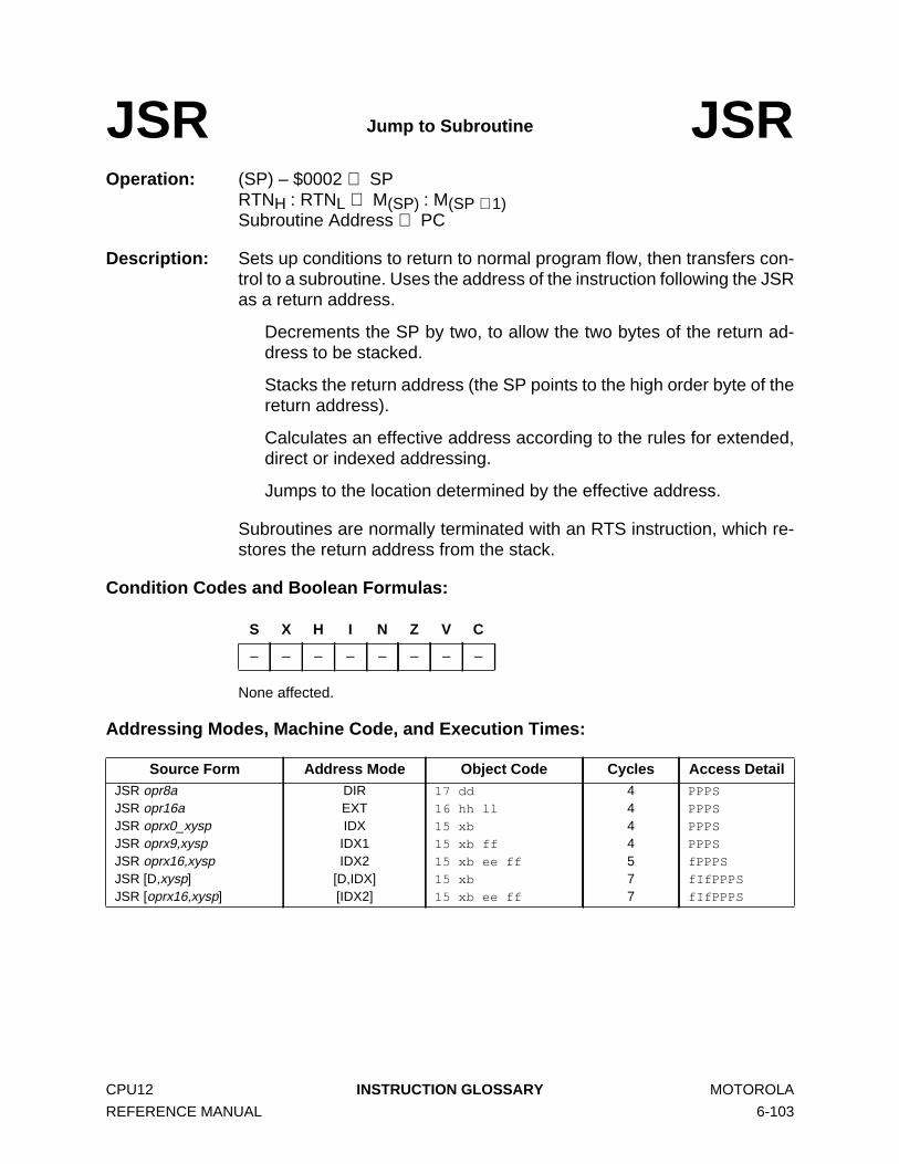
Operation: (SP) – $0002 ⇒ SPRTNH : RTNL ⇒ M(SP) : M(SP + 1)Subroutine Address ⇒ PC
Description: Sets up conditions to return to normal program flow, then transfers con-trol to a subroutine. Uses the address of the instruction following the JSRas a return address.
Decrements the SP by two, to allow the two bytes of the return ad-dress to be stacked.
Stacks the return address (the SP points to the high order byte of thereturn address).
Calculates an effective address according to the rules for extended,direct or indexed addressing.
Jumps to the location determined by the effective address.
Subroutines are normally terminated with an RTS instruction, which re-stores the return address from the stack.
Condition Codes and Boolean Formulas:
None affected.
Addressing Modes, Machine Code, and Execution Times:
JSR Jump to Subroutine JSR
S X H I N Z V C
– – – – – – – –
Source Form Address Mode Object Code Cycles Access DetailJSR opr8aJSR opr16aJSR oprx0_xyspJSR oprx9,xyspJSR oprx16,xyspJSR [D,xysp]JSR [oprx16,xysp]
DIREXTIDXIDX1IDX2
[D,IDX][IDX2]
17 dd
16 hh ll
15 xb
15 xb ff
15 xb ee ff
15 xb
15 xb ee ff
4444577
PPPS
PPPS
PPPS
PPPS
fPPPS
fIfPPPS
fIfPPPS
CPU12 INSTRUCTION GLOSSARY MOTOROLA
REFERENCE MANUAL 6-103
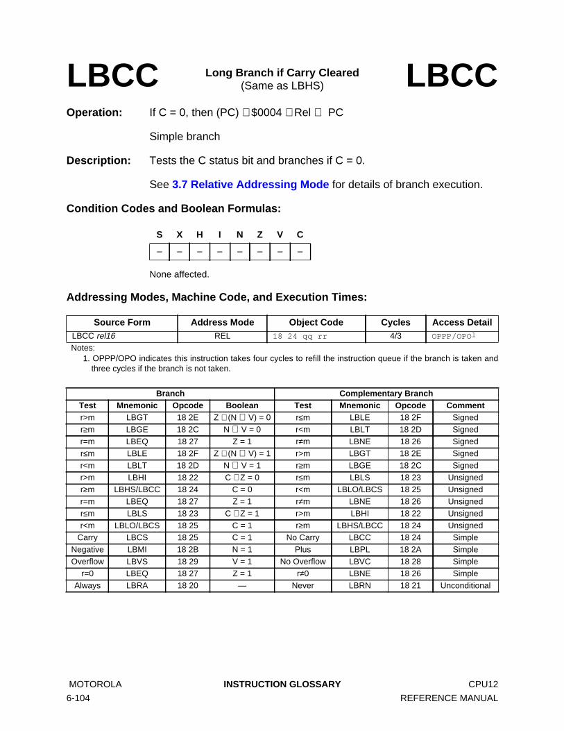
Operation: If C = 0, then (PC) + $0004 + Rel ⇒ PC
Simple branch
Description: Tests the C status bit and branches if C = 0.
See 3.7 Relative Addressing Mode for details of branch execution.
Condition Codes and Boolean Formulas:
None affected.
Addressing Modes, Machine Code, and Execution Times:
LBCC Long Branch if Carry Cleared(Same as LBHS) LBCC
S X H I N Z V C
– – – – – – – –
Source Form Address Mode Object Code Cycles Access DetailLBCC rel16 REL 18 24 qq rr 4/3 OPPP/OPO1
Notes:1. OPPP/OPO indicates this instruction takes four cycles to refill the instruction queue if the branch is taken and
three cycles if the branch is not taken.
Branch Complementary BranchTest Mnemonic Opcode Boolean Test Mnemonic Opcode Commentr>m LBGT 18 2E Z + (N ⊕ V) = 0 r≤m LBLE 18 2F Signedr≥m LBGE 18 2C N ⊕ V = 0 r<m LBLT 18 2D Signedr=m LBEQ 18 27 Z = 1 r≠m LBNE 18 26 Signedr≤m LBLE 18 2F Z + (N ⊕ V) = 1 r>m LBGT 18 2E Signedr<m LBLT 18 2D N ⊕ V = 1 r≥m LBGE 18 2C Signedr>m LBHI 18 22 C + Z = 0 r≤m LBLS 18 23 Unsignedr≥m LBHS/LBCC 18 24 C = 0 r<m LBLO/LBCS 18 25 Unsignedr=m LBEQ 18 27 Z = 1 r≠m LBNE 18 26 Unsignedr≤m LBLS 18 23 C + Z = 1 r>m LBHI 18 22 Unsignedr<m LBLO/LBCS 18 25 C = 1 r≥m LBHS/LBCC 18 24 Unsigned
Carry LBCS 18 25 C = 1 No Carry LBCC 18 24 SimpleNegative LBMI 18 2B N = 1 Plus LBPL 18 2A SimpleOverflow LBVS 18 29 V = 1 No Overflow LBVC 18 28 Simple
r=0 LBEQ 18 27 Z = 1 r≠0 LBNE 18 26 SimpleAlways LBRA 18 20 — Never LBRN 18 21 Unconditional
MOTOROLA INSTRUCTION GLOSSARY CPU12
6-104 REFERENCE MANUAL

Operation: If C = 1, then (PC) + $0004 + Rel ⇒ PC
Simple branch
Description: Tests the C status bit and branches if C = 1.
See 3.7 Relative Addressing Mode for details of branch execution.
Condition Codes and Boolean Formulas:
None affected.
Addressing Modes, Machine Code, and Execution Times:
LBCS Long Branch if Carry Set(Same as LBLO) LBCS
S X H I N Z V C
– – – – – – – –
Source Form Address Mode Object Code Cycles Access DetailLBCS rel16 REL 18 25 qq rr 4/3 OPPP/OPO1
Notes:1. OPPP/OPO indicates this instruction takes four cycles to refill the instruction queue if the branch is taken and
three cycles if the branch is not taken.
Branch Complementary BranchTest Mnemonic Opcode Boolean Test Mnemonic Opcode Commentr>m LBGT 18 2E Z + (N ⊕ V) = 0 r≤m LBLE 18 2F Signedr≥m LBGE 18 2C N ⊕ V = 0 r<m LBLT 18 2D Signedr=m LBEQ 18 27 Z = 1 r≠m LBNE 18 26 Signedr≤m LBLE 18 2F Z + (N ⊕ V) = 1 r>m LBGT 18 2E Signedr<m LBLT 18 2D N ⊕ V = 1 r≥m LBGE 18 2C Signedr>m LBHI 18 22 C + Z = 0 r≤m LBLS 18 23 Unsignedr≥m LBHS/LBCC 18 24 C = 0 r<m LBLO/LBCS 18 25 Unsignedr=m LBEQ 18 27 Z = 1 r≠m LBNE 18 26 Unsignedr≤m LBLS 18 23 C + Z = 1 r>m LBHI 18 22 Unsignedr<m LBLO/LBCS 18 25 C = 1 r≥m LBHS/LBCC 18 24 Unsigned
Carry LBCS 18 25 C = 1 No Carry LBCC 18 24 SimpleNegative LBMI 18 2B N = 1 Plus LBPL 18 2A SimpleOverflow LBVS 18 29 V = 1 No Overflow LBVC 18 28 Simple
r=0 LBEQ 18 27 Z = 1 r≠0 LBNE 18 26 SimpleAlways LBRA 18 20 — Never LBRN 18 21 Unconditional
CPU12 INSTRUCTION GLOSSARY MOTOROLA
REFERENCE MANUAL 6-105

Operation: If Z = 1, (PC) + $0004 + Rel ⇒ PC
Simple branch
Description: Tests the Z status bit and branches if Z = 1.
See 3.7 Relative Addressing Mode for details of branch execution.
Condition Codes and Boolean Formulas:
None affected.
Addressing Modes, Machine Code, and Execution Times:
LBEQ Long Branch if Equal LBEQ
S X H I N Z V C
– – – – – – – –
Source Form Address Mode Object Code Cycles Access DetailLBEQ rel16 REL 18 27 qq rr 4/3 OPPP/OPO1
Notes:1. OPPP/OPO indicates this instruction takes four cycles to refill the instruction queue if the branch is taken and
three cycles if the branch is not taken.
Branch Complementary BranchTest Mnemonic Opcode Boolean Test Mnemonic Opcode Commentr>m LBGT 18 2E Z + (N ⊕ V) = 0 r≤m LBLE 18 2F Signedr≥m LBGE 18 2C N ⊕ V = 0 r<m LBLT 18 2D Signedr=m LBEQ 18 27 Z = 1 r≠m LBNE 18 26 Signedr≤m LBLE 18 2F Z + (N ⊕ V) = 1 r>m LBGT 18 2E Signedr<m LBLT 18 2D N ⊕ V = 1 r≥m LBGE 18 2C Signedr>m LBHI 18 22 C + Z = 0 r≤m LBLS 18 23 Unsignedr≥m LBHS/LBCC 18 24 C = 0 r<m LBLO/LBCS 18 25 Unsignedr=m LBEQ 18 27 Z = 1 r≠m LBNE 18 26 Unsignedr≤m LBLS 18 23 C + Z = 1 r>m LBHI 18 22 Unsignedr<m LBLO/LBCS 18 25 C = 1 r≥m LBHS/LBCC 18 24 Unsigned
Carry LBCS 18 25 C = 1 No Carry LBCC 18 24 SimpleNegative LBMI 18 2B N = 1 Plus LBPL 18 2A SimpleOverflow LBVS 18 29 V = 1 No Overflow LBVC 18 28 Simple
r=0 LBEQ 18 27 Z = 1 r≠0 LBNE 18 26 SimpleAlways LBRA 18 20 — Never LBRN 18 21 Unconditional
MOTOROLA INSTRUCTION GLOSSARY CPU12
6-106 REFERENCE MANUAL

Operation: If N ⊕ V = 0, (PC) + $0004 + Rel ⇒ PC
For signed two’s complement numbers,if (Accumulator) ≥ Memory), then branch
Description: If LBGE is executed immediately after execution of CBA, CMPA, CMPB,CMPD, CPX, CPY, SBA, SUBA, SUBB, or SUBD, a branch occurs if andonly if the two’s complement number in the accumulator was greaterthan or equal to the two’s complement number in memory.
See 3.7 Relative Addressing Mode for details of branch execution.
Condition Codes and Boolean Formulas:
None affected.
Addressing Modes, Machine Code, and Execution Times:
LBGE Long Branch if Greater Than or Equal toZero LBGE
S X H I N Z V C
– – – – – – – –
Source Form Address Mode Object Code Cycles Access DetailLBGE rel16 REL 18 2C qq rr 4/3 OPPP/OPO1
Notes:1. OPPP/OPO indicates this instruction takes four cycles to refill the instruction queue if the branch is taken and
three cycles if the branch is not taken.
Branch Complementary BranchTest Mnemonic Opcode Boolean Test Mnemonic Opcode Commentr>m LBGT 18 2E Z + (N ⊕ V) = 0 r≤m LBLE 18 2F Signedr≥m LBGE 18 2C N ⊕ V = 0 r<m LBLT 18 2D Signedr=m LBEQ 18 27 Z = 1 r≠m LBNE 18 26 Signedr≤m LBLE 18 2F Z + (N ⊕ V) = 1 r>m LBGT 18 2E Signedr<m LBLT 18 2D N ⊕ V = 1 r≥m LBGE 18 2C Signedr>m LBHI 18 22 C + Z = 0 r≤m LBLS 18 23 Unsignedr≥m LBHS/LBCC 18 24 C = 0 r<m LBLO/LBCS 18 25 Unsignedr=m LBEQ 18 27 Z = 1 r≠m LBNE 18 26 Unsignedr≤m LBLS 18 23 C + Z = 1 r>m LBHI 18 22 Unsignedr<m LBLO/LBCS 18 25 C = 1 r≥m LBHS/LBCC 18 24 Unsigned
Carry LBCS 18 25 C = 1 No Carry LBCC 18 24 SimpleNegative LBMI 18 2B N = 1 Plus LBPL 18 2A SimpleOverflow LBVS 18 29 V = 1 No Overflow LBVC 18 28 Simple
r=0 LBEQ 18 27 Z = 1 r≠0 LBNE 18 26 SimpleAlways LBRA 18 20 — Never LBRN 18 21 Unconditional
CPU12 INSTRUCTION GLOSSARY MOTOROLA
REFERENCE MANUAL 6-107
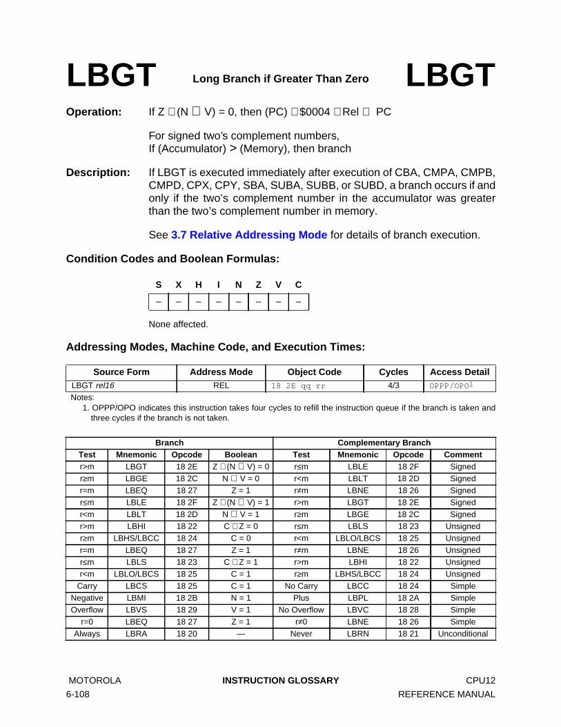
Operation: If Z + (N ⊕ V) = 0, then (PC) + $0004 + Rel ⇒ PC
For signed two’s complement numbers,If (Accumulator) > (Memory), then branch
Description: If LBGT is executed immediately after execution of CBA, CMPA, CMPB,CMPD, CPX, CPY, SBA, SUBA, SUBB, or SUBD, a branch occurs if andonly if the two’s complement number in the accumulator was greaterthan the two’s complement number in memory.
See 3.7 Relative Addressing Mode for details of branch execution.
Condition Codes and Boolean Formulas:
None affected.
Addressing Modes, Machine Code, and Execution Times:
LBGT Long Branch if Greater Than Zero LBGT
S X H I N Z V C
– – – – – – – –
Source Form Address Mode Object Code Cycles Access DetailLBGT rel16 REL 18 2E qq rr 4/3 OPPP/OPO1
Notes:1. OPPP/OPO indicates this instruction takes four cycles to refill the instruction queue if the branch is taken and
three cycles if the branch is not taken.
Branch Complementary BranchTest Mnemonic Opcode Boolean Test Mnemonic Opcode Commentr>m LBGT 18 2E Z + (N ⊕ V) = 0 r≤m LBLE 18 2F Signedr≥m LBGE 18 2C N ⊕ V = 0 r<m LBLT 18 2D Signedr=m LBEQ 18 27 Z = 1 r≠m LBNE 18 26 Signedr≤m LBLE 18 2F Z + (N ⊕ V) = 1 r>m LBGT 18 2E Signedr<m LBLT 18 2D N ⊕ V = 1 r≥m LBGE 18 2C Signedr>m LBHI 18 22 C + Z = 0 r≤m LBLS 18 23 Unsignedr≥m LBHS/LBCC 18 24 C = 0 r<m LBLO/LBCS 18 25 Unsignedr=m LBEQ 18 27 Z = 1 r≠m LBNE 18 26 Unsignedr≤m LBLS 18 23 C + Z = 1 r>m LBHI 18 22 Unsignedr<m LBLO/LBCS 18 25 C = 1 r≥m LBHS/LBCC 18 24 Unsigned
Carry LBCS 18 25 C = 1 No Carry LBCC 18 24 SimpleNegative LBMI 18 2B N = 1 Plus LBPL 18 2A SimpleOverflow LBVS 18 29 V = 1 No Overflow LBVC 18 28 Simple
r=0 LBEQ 18 27 Z = 1 r≠0 LBNE 18 26 SimpleAlways LBRA 18 20 — Never LBRN 18 21 Unconditional
MOTOROLA INSTRUCTION GLOSSARY CPU12
6-108 REFERENCE MANUAL

Operation: If C + Z = 0, then (PC) + $0004 + Rel ⇒ PC
For unsigned binary numbers, if (Accumulator) > (Memory), then branch
Description: If LBHI is executed immediately after execution of CBA, CMPA, CMPB,CMPD, CPX, CPY, SBA, SUBA, SUBB, or SUBD, a branch occurs if andonly if the unsigned binary number in the accumulator was greater thanthe unsigned binary number in memory. This instruction is generally notuseful after INC/DEC, LD/ST, TST/CLR/COM because these instruc-tions do not affect the C status bit.
See 3.7 Relative Addressing Mode for details of branch execution.
Condition Codes and Boolean Formulas:
None affected.
Addressing Modes, Machine Code, and Execution Times:
LBHI Long Branch if Higher LBHI
S X H I N Z V C
– – – – – – – –
Source Form Address Mode Object Code Cycles Access DetailLBHI rel16 REL 18 22 qq rr 4/3 OPPP/OPO1
Notes:1. OPPP/OPO indicates this instruction takes four cycles to refill the instruction queue if the branch is taken and
three cycles if the branch is not taken.
Branch Complementary BranchTest Mnemonic Opcode Boolean Test Mnemonic Opcode Commentr>m LBGT 18 2E Z + (N ⊕ V) = 0 r≤m LBLE 18 2F Signedr≥m LBGE 18 2C N ⊕ V = 0 r<m LBLT 18 2D Signedr=m LBEQ 18 27 Z = 1 r≠m LBNE 18 26 Signedr≤m LBLE 18 2F Z + (N ⊕ V) = 1 r>m LBGT 18 2E Signedr<m LBLT 18 2D N ⊕ V = 1 r≥m LBGE 18 2C Signedr>m LBHI 18 22 C + Z = 0 r≤m LBLS 18 23 Unsignedr≥m LBHS/LBCC 18 24 C = 0 r<m LBLO/LBCS 18 25 Unsignedr=m LBEQ 18 27 Z = 1 r≠m LBNE 18 26 Unsignedr≤m LBLS 18 23 C + Z = 1 r>m LBHI 18 22 Unsignedr<m LBLO/LBCS 18 25 C = 1 r≥m LBHS/LBCC 18 24 Unsigned
Carry LBCS 18 25 C = 1 No Carry LBCC 18 24 SimpleNegative LBMI 18 2B N = 1 Plus LBPL 18 2A SimpleOverflow LBVS 18 29 V = 1 No Overflow LBVC 18 28 Simple
r=0 LBEQ 18 27 Z = 1 r≠0 LBNE 18 26 SimpleAlways LBRA 18 20 — Never LBRN 18 21 Unconditional
CPU12 INSTRUCTION GLOSSARY MOTOROLA
REFERENCE MANUAL 6-109

Operation: If C = 0, then (PC) + $0004 + Rel ⇒ PC
For unsigned binary numbers, if (Accumulator) ≥ (Memory), then branch
Description: If LBHS is executed immediately after execution of CBA, CMPA, CMPB,CMPD, CPX, CPY, SBA, SUBA, SUBB, or SUBD, a branch occurs if andonly if the unsigned binary number in the accumulator was greater thanor equal to the unsigned binary number in memory. This instruction isgenerally not useful after INC/DEC, LD/ST, TST/CLR/COM becausethese instructions do not affect the C status bit.
See 3.7 Relative Addressing Mode for details of branch execution.
Condition Codes and Boolean Formulas:
None affected.
Addressing Modes, Machine Code, and Execution Times:
LBHS Long Branch if Higher or Same(Same as LBCC) LBHS
S X H I N Z V C
– – – – – – – –
Source Form Address Mode Object Code Cycles Access DetailLBHS rel16 REL 18 24 qq rr 4/3 OPPP/OPO1
Notes:1. OPPP/OPO indicates this instruction takes four cycles to refill the instruction queue if the branch is taken and
three cycles if the branch is not taken.
Branch Complementary BranchTest Mnemonic Opcode Boolean Test Mnemonic Opcode Commentr>m LBGT 18 2E Z + (N ⊕ V) = 0 r≤m LBLE 18 2F Signedr≥m LBGE 18 2C N ⊕ V = 0 r<m LBLT 18 2D Signedr=m LBEQ 18 27 Z = 1 r≠m LBNE 18 26 Signedr≤m LBLE 18 2F Z + (N ⊕ V) = 1 r>m LBGT 18 2E Signedr<m LBLT 18 2D N ⊕ V = 1 r≥m LBGE 18 2C Signedr>m LBHI 18 22 C + Z = 0 r≤m LBLS 18 23 Unsignedr≥m LBHS/LBCC 18 24 C = 0 r<m LBLO/LBCS 18 25 Unsignedr=m LBEQ 18 27 Z = 1 r≠m LBNE 18 26 Unsignedr≤m LBLS 18 23 C + Z = 1 r>m LBHI 18 22 Unsignedr<m LBLO/LBCS 18 25 C = 1 r≥m LBHS/LBCC 18 24 Unsigned
Carry LBCS 18 25 C = 1 No Carry LBCC 18 24 SimpleNegative LBMI 18 2B N = 1 Plus LBPL 18 2A SimpleOverflow LBVS 18 29 V = 1 No Overflow LBVC 18 28 Simple
r=0 LBEQ 18 27 Z = 1 r≠0 LBNE 18 26 SimpleAlways LBRA 18 20 — Never LBRN 18 21 Unconditional
MOTOROLA INSTRUCTION GLOSSARY CPU12
6-110 REFERENCE MANUAL

Operation: If Z + (N ⊕ V) = 1, then (PC) + $0004 + Rel ⇒ PC
For signed two’s complement numbers,if (Accumulator) ≤ (Memory), then branch
Description: If LBLE is executed immediately after execution of CBA, CMPA, CMPB,CMPD, CPX, CPY, SBA, SUBA, SUBB, or SUBD, a branch occurs if andonly if the two’s complement number in the accumulator was less thanor equal to the two’s complement number in memory.
See 3.7 Relative Addressing Mode for details of branch execution.
Condition Codes and Boolean Formulas:
None affected.
Addressing Modes, Machine Code, and Execution Times:
LBLE Long Branch if Less Than orEqual to Zero LBLE
S X H I N Z V C
– – – – – – – –
Source Form Address Mode Object Code Cycles Access DetailLBLE rel16 REL 18 2F qq rr 4/3 OPPP/OPO1
Notes:1. OPPP/OPO indicates this instruction takes four cycles to refill the instruction queue if the branch is taken and
three cycles if the branch is not taken.
Branch Complementary BranchTest Mnemonic Opcode Boolean Test Mnemonic Opcode Commentr>m LBGT 18 2E Z + (N ⊕ V) = 0 r≤m LBLE 18 2F Signedr≥m LBGE 18 2C N ⊕ V = 0 r<m LBLT 18 2D Signedr=m LBEQ 18 27 Z = 1 r≠m LBNE 18 26 Signedr≤m LBLE 18 2F Z + (N ⊕ V) = 1 r>m LBGT 18 2E Signedr<m LBLT 18 2D N ⊕ V = 1 r≥m LBGE 18 2C Signedr>m LBHI 18 22 C + Z = 0 r≤m LBLS 18 23 Unsignedr≥m LBHS/LBCC 18 24 C = 0 r<m LBLO/LBCS 18 25 Unsignedr=m LBEQ 18 27 Z = 1 r≠m LBNE 18 26 Unsignedr≤m LBLS 18 23 C + Z = 1 r>m LBHI 18 22 Unsignedr<m LBLO/LBCS 18 25 C = 1 r≥m LBHS/LBCC 18 24 Unsigned
Carry LBCS 18 25 C = 1 No Carry LBCC 18 24 SimpleNegative LBMI 18 2B N = 1 Plus LBPL 18 2A SimpleOverflow LBVS 18 29 V = 1 No Overflow LBVC 18 28 Simple
r=0 LBEQ 18 27 Z = 1 r≠0 LBNE 18 26 SimpleAlways LBRA 18 20 — Never LBRN 18 21 Unconditional
CPU12 INSTRUCTION GLOSSARY MOTOROLA
REFERENCE MANUAL 6-111

Operation: If C = 1, then (PC) + $0004 + Rel ⇒ PC
For unsigned binary numbers, if (Accumulator) < (Memory), then branch
Description: If LBLO is executed immediately after execution of CBA, CMPA, CMPB,CMPD, CPX, CPY, SBA, SUBA, SUBB, or SUBD, a branch occurs if andonly if the unsigned binary number in the accumulator was less than theunsigned binary number in memory. This instruction is generally not use-ful after INC/DEC, LD/ST, TST/CLR/COM because these instructions donot affect the C status bit.
See 3.7 Relative Addressing Mode for details of branch execution.
Condition Codes and Boolean Formulas:
None affected.
Addressing Modes, Machine Code, and Execution Times:
LBLO Long Branch if Lower(Same as LBCS) LBLO
S X H I N Z V C
– – – – – – – –
Source Form Address Mode Object Code Cycles Access DetailLBLO rel16 REL 18 25 qq rr 4/3 OPPP/OPO1
Notes:1. OPPP/OPO indicates this instruction takes four cycles to refill the instruction queue if the branch is taken and
three cycles if the branch is not taken.
Branch Complementary BranchTest Mnemonic Opcode Boolean Test Mnemonic Opcode Commentr>m LBGT 18 2E Z + (N ⊕ V) = 0 r≤m LBLE 18 2F Signedr≥m LBGE 18 2C N ⊕ V = 0 r<m LBLT 18 2D Signedr=m LBEQ 18 27 Z = 1 r≠m LBNE 18 26 Signedr≤m LBLE 18 2F Z + (N ⊕ V) = 1 r>m LBGT 18 2E Signedr<m LBLT 18 2D N ⊕ V = 1 r≥m LBGE 18 2C Signedr>m LBHI 18 22 C + Z = 0 r≤m LBLS 18 23 Unsignedr≥m LBHS/LBCC 18 24 C = 0 r<m LBLO/LBCS 18 25 Unsignedr=m LBEQ 18 27 Z = 1 r≠m LBNE 18 26 Unsignedr≤m LBLS 18 23 C + Z = 1 r>m LBHI 18 22 Unsignedr<m LBLO/LBCS 18 25 C = 1 r≥m LBHS/LBCC 18 24 Unsigned
Carry LBCS 18 25 C = 1 No Carry LBCC 18 24 SimpleNegative LBMI 18 2B N = 1 Plus LBPL 18 2A SimpleOverflow LBVS 18 29 V = 1 No Overflow LBVC 18 28 Simple
r=0 LBEQ 18 27 Z = 1 r≠0 LBNE 18 26 SimpleAlways LBRA 18 20 — Never LBRN 18 21 Unconditional
MOTOROLA INSTRUCTION GLOSSARY CPU12
6-112 REFERENCE MANUAL

Operation: If C + Z = 1, then (PC) + $0004 + Rel ⇒ PC
For unsigned binary numbers, if (Accumulator) ≤ (Memory), then branch
Description: If LBLS is executed immediately after execution of CBA, CMPA, CMPB,CMPD, CPX, CPY, SBA, SUBA, SUBB, or SUBD, a branch occurs if andonly if the unsigned binary number in the accumulator was less than orequal to the unsigned binary number in memory. This instruction is gen-erally not useful after INC/DEC, LD/ST, TST/CLR/COM because theseinstructions do not affect the C status bit.
See 3.7 Relative Addressing Mode for details of branch execution.
Condition Codes and Boolean Formulas:
None affected.
Addressing Modes, Machine Code, and Execution Times:
LBLS Long Branch if Lower or Same LBLS
S X H I N Z V C
– – – – – – – –
Source Form Address Mode Object Code Cycles Access DetailLBLS rel16 REL 18 23 qq rr 4/3 OPPP/OPO1
Notes:1. OPPP/OPO indicates this instruction takes four cycles to refill the instruction queue if the branch is taken and
three cycles if the branch is not taken.
Branch Complementary BranchTest Mnemonic Opcode Boolean Test Mnemonic Opcode Commentr>m LBGT 18 2E Z + (N ⊕ V) = 0 r≤m LBLE 18 2F Signedr≥m LBGE 18 2C N ⊕ V = 0 r<m LBLT 18 2D Signedr=m LBEQ 18 27 Z = 1 r≠m LBNE 18 26 Signedr≤m LBLE 18 2F Z + (N ⊕ V) = 1 r>m LBGT 18 2E Signedr<m LBLT 18 2D N ⊕ V = 1 r≥m LBGE 18 2C Signedr>m LBHI 18 22 C + Z = 0 r≤m LBLS 18 23 Unsignedr≥m LBHS/LBCC 18 24 C = 0 r<m LBLO/LBCS 18 25 Unsignedr=m LBEQ 18 27 Z = 1 r≠m LBNE 18 26 Unsignedr≤m LBLS 18 23 C + Z = 1 r>m LBHI 18 22 Unsignedr<m LBLO/LBCS 18 25 C = 1 r≥m LBHS/LBCC 18 24 Unsigned
Carry LBCS 18 25 C = 1 No Carry LBCC 18 24 SimpleNegative LBMI 18 2B N = 1 Plus LBPL 18 2A SimpleOverflow LBVS 18 29 V = 1 No Overflow LBVC 18 28 Simple
r=0 LBEQ 18 27 Z = 1 r≠0 LBNE 18 26 SimpleAlways LBRA 18 20 — Never LBRN 18 21 Unconditional
CPU12 INSTRUCTION GLOSSARY MOTOROLA
REFERENCE MANUAL 6-113

Operation: If N ⊕ V = 1, (PC) + $0004 + Rel ⇒ PC
For signed two’s complement numbers,if (Accumulator) < (Memory), then branch
Description: If LBLT is executed immediately after execution of CBA, CMPA, CMPB,CMPD, CPX, CPY, SBA, SUBA, SUBB, or SUBD, a branch occurs if andonly if the two’s complement number in the accumulator was less thanthe two’s complement number in memory.
See 3.7 Relative Addressing Mode for details of branch execution.
Condition Codes and Boolean Formulas:
None affected.
Addressing Modes, Machine Code, and Execution Times:
LBLT Long Branch if Less Than Zero LBLT
S X H I N Z V C
– – – – – – – –
Source Form Address Mode Object Code Cycles Access DetailLBLT rel16 REL 18 2D qq rr 4/3 OPPP/OPO1
Notes:1. OPPP/OPO indicates this instruction takes four cycles to refill the instruction queue if the branch is taken and
three cycles if the branch is not taken.
Branch Complementary BranchTest Mnemonic Opcode Boolean Test Mnemonic Opcode Commentr>m LBGT 18 2E Z + (N ⊕ V) = 0 r≤m LBLE 18 2F Signedr≥m LBGE 18 2C N ⊕ V = 0 r<m LBLT 18 2D Signedr=m LBEQ 18 27 Z = 1 r≠m LBNE 18 26 Signedr≤m LBLE 18 2F Z + (N ⊕ V) = 1 r>m LBGT 18 2E Signedr<m LBLT 18 2D N ⊕ V = 1 r≥m LBGE 18 2C Signedr>m LBHI 18 22 C + Z = 0 r≤m LBLS 18 23 Unsignedr≥m LBHS/LBCC 18 24 C = 0 r<m LBLO/LBCS 18 25 Unsignedr=m LBEQ 18 27 Z = 1 r≠m LBNE 18 26 Unsignedr≤m LBLS 18 23 C + Z = 1 r>m LBHI 18 22 Unsignedr<m LBLO/LBCS 18 25 C = 1 r≥m LBHS/LBCC 18 24 Unsigned
Carry LBCS 18 25 C = 1 No Carry LBCC 18 24 SimpleNegative LBMI 18 2B N = 1 Plus LBPL 18 2A SimpleOverflow LBVS 18 29 V = 1 No Overflow LBVC 18 28 Simple
r=0 LBEQ 18 27 Z = 1 r≠0 LBNE 18 26 SimpleAlways LBRA 18 20 — Never LBRN 18 21 Unconditional
MOTOROLA INSTRUCTION GLOSSARY CPU12
6-114 REFERENCE MANUAL

Operation: If N = 1, then (PC) + $0004 + Rel ⇒ PC
Simple branch
Description: Tests the N status bit and branches if N = 1.
See 3.7 Relative Addressing Mode for details of branch execution.
Condition Codes and Boolean Formulas:
None affected.
Addressing Modes, Machine Code, and Execution Times:
LBMI Long Branch if Minus LBMI
S X H I N Z V C
– – – – – – – –
Source Form Address Mode Object Code Cycles Access DetailLBMI rel16 REL 18 2B qq rr 4/3 OPPP/OPO1
Notes:1. OPPP/OPO indicates this instruction takes four cycles to refill the instruction queue if the branch is taken and
three cycles if the branch is not taken.
Branch Complementary BranchTest Mnemonic Opcode Boolean Test Mnemonic Opcode Commentr>m LBGT 18 2E Z + (N ⊕ V) = 0 r≤m LBLE 18 2F Signedr≥m LBGE 18 2C N ⊕ V = 0 r<m LBLT 18 2D Signedr=m LBEQ 18 27 Z = 1 r≠m LBNE 18 26 Signedr≤m LBLE 18 2F Z + (N ⊕ V) = 1 r>m LBGT 18 2E Signedr<m LBLT 18 2D N ⊕ V = 1 r≥m LBGE 18 2C Signedr>m LBHI 18 22 C + Z = 0 r≤m LBLS 18 23 Unsignedr≥m LBHS/LBCC 18 24 C = 0 r<m LBLO/LBCS 18 25 Unsignedr=m LBEQ 18 27 Z = 1 r≠m LBNE 18 26 Unsignedr≤m LBLS 18 23 C + Z = 1 r>m LBHI 18 22 Unsignedr<m LBLO/LBCS 18 25 C = 1 r≥m LBHS/LBCC 18 24 Unsigned
Carry LBCS 18 25 C = 1 No Carry LBCC 18 24 SimpleNegative LBMI 18 2B N = 1 Plus LBPL 18 2A SimpleOverflow LBVS 18 29 V = 1 No Overflow LBVC 18 28 Simple
r=0 LBEQ 18 27 Z = 1 r≠0 LBNE 18 26 SimpleAlways LBRA 18 20 — Never LBRN 18 21 Unconditional
CPU12 INSTRUCTION GLOSSARY MOTOROLA
REFERENCE MANUAL 6-115

Operation: If Z = 0, then (PC) + $0004 + Rel ⇒ PC
Simple branch
Description: Tests the Z status bit and branches if Z = 0.
See 3.7 Relative Addressing Mode for details of branch execution.
Condition Codes and Boolean Formulas:
None affected.
Addressing Modes, Machine Code, and Execution Times:
LBNE Long Branch if Not Equal to Zero LBNE
S X H I N Z V C
– – – – – – – –
Source Form Address Mode Object Code Cycles Access DetailLBNE rel16 REL 18 26 qq rr 4/3 OPPP/OPO1
Notes:1. OPPP/OPO indicates this instruction takes four cycles to refill the instruction queue if the branch is taken and
three cycles if the branch is not taken.
Branch Complementary BranchTest Mnemonic Opcode Boolean Test Mnemonic Opcode Commentr>m LBGT 18 2E Z + (N ⊕ V) = 0 r≤m LBLE 18 2F Signedr≥m LBGE 18 2C N ⊕ V = 0 r<m LBLT 18 2D Signedr=m LBEQ 18 27 Z = 1 r≠m LBNE 18 26 Signedr≤m LBLE 18 2F Z + (N ⊕ V) = 1 r>m LBGT 18 2E Signedr<m LBLT 18 2D N ⊕ V = 1 r≥m LBGE 18 2C Signedr>m LBHI 18 22 C + Z = 0 r≤m LBLS 18 23 Unsignedr≥m LBHS/LBCC 18 24 C = 0 r<m LBLO/LBCS 18 25 Unsignedr=m LBEQ 18 27 Z = 1 r≠m LBNE 18 26 Unsignedr≤m LBLS 18 23 C + Z = 1 r>m LBHI 18 22 Unsignedr<m LBLO/LBCS 18 25 C = 1 r≥m LBHS/LBCC 18 24 Unsigned
Carry LBCS 18 25 C = 1 No Carry LBCC 18 24 SimpleNegative LBMI 18 2B N = 1 Plus LBPL 18 2A SimpleOverflow LBVS 18 29 V = 1 No Overflow LBVC 18 28 Simple
r=0 LBEQ 18 27 Z = 1 r≠0 LBNE 18 26 SimpleAlways LBRA 18 20 — Never LBRN 18 21 Unconditional
MOTOROLA INSTRUCTION GLOSSARY CPU12
6-116 REFERENCE MANUAL

Operation: If N = 0, then (PC) + $0004 + Rel ⇒ PC
Simple branch
Description: Tests the N status bit and branches if N = 0.
See 3.7 Relative Addressing Mode for details of branch execution.
Condition Codes and Boolean Formulas:
None affected.
Addressing Modes, Machine Code, and Execution Times:
LBPL Long Branch if Plus LBPL
S X H I N Z V C
– – – – – – – –
Source Form Address Mode Object Code Cycles Access DetailLBPL rel16 REL 18 2A qq rr 4/3 OPPP/OPO1
Notes:1. OPPP/OPO indicates this instruction takes four cycles to refill the instruction queue if the branch is taken and
three cycles if the branch is not taken.
Branch Complementary BranchTest Mnemonic Opcode Boolean Test Mnemonic Opcode Commentr>m LBGT 18 2E Z + (N ⊕ V) = 0 r≤m LBLE 18 2F Signedr≥m LBGE 18 2C N ⊕ V = 0 r<m LBLT 18 2D Signedr=m LBEQ 18 27 Z = 1 r≠m LBNE 18 26 Signedr≤m LBLE 18 2F Z + (N ⊕ V) = 1 r>m LBGT 18 2E Signedr<m LBLT 18 2D N ⊕ V = 1 r≥m LBGE 18 2C Signedr>m LBHI 18 22 C + Z = 0 r≤m LBLS 18 23 Unsignedr≥m LBHS/LBCC 18 24 C = 0 r<m LBLO/LBCS 18 25 Unsignedr=m LBEQ 18 27 Z = 1 r≠m LBNE 18 26 Unsignedr≤m LBLS 18 23 C + Z = 1 r>m LBHI 18 22 Unsignedr<m LBLO/LBCS 18 25 C = 1 r≥m LBHS/LBCC 18 24 Unsigned
Carry LBCS 18 25 C = 1 No Carry LBCC 18 24 SimpleNegative LBMI 18 2B N = 1 Plus LBPL 18 2A SimpleOverflow LBVS 18 29 V = 1 No Overflow LBVC 18 28 Simple
r=0 LBEQ 18 27 Z = 1 r≠0 LBNE 18 26 SimpleAlways LBRA 18 20 — Never LBRN 18 21 Unconditional
CPU12 INSTRUCTION GLOSSARY MOTOROLA
REFERENCE MANUAL 6-117

Operation: (PC) + $0004 + Rel ⇒ PC
Description: Unconditional branch to an address calculated as shown in the expres-sion. Rel is a relative offset stored as a two’s complement number in thesecond and third bytes of machine code corresponding to the longbranch instruction.
Execution time is longer when a conditional branch is taken than whenit is not, because the instruction queue must be refilled before executionresumes at the new address. Since the LBRA branch condition is alwayssatisfied, the branch is always taken, and the instruction queue must al-ways be refilled, so execution time is always the larger value.
See 3.7 Relative Addressing Mode for details of branch execution.
Condition Codes and Boolean Formulas:
None affected.
Addressing Modes, Machine Code, and Execution Times:
LBRA Long Branch Always LBRA
S X H I N Z V C
– – – – – – – –
Source Form Address Mode Object Code Cycles Access DetailLBRA rel16 REL 18 20 qq rr 4 OPPP
MOTOROLA INSTRUCTION GLOSSARY CPU12
6-118 REFERENCE MANUAL

Operation: (PC) + $0004 ⇒ PC
Description: Never branches. LBRN is effectively a 4-byte NOP that requires threecycles to execute. LBRN is included in the instruction set to provide acomplement to the LBRA instruction. The instruction is useful during pro-gram debug, to negate the effect of another branch instruction withoutdisturbing the offset byte. A complement for LBRA is also useful in com-piler implementations.
Execution time is longer when a conditional branch is taken than whenit is not, because the instruction queue must be refilled before executionresumes at the new address. Since the LBRN branch condition is neversatisfied, the branch is never taken, and the queue does not need to berefilled, so execution time is always the smaller value.
Condition Codes and Boolean Formulas:
None affected.
Addressing Modes, Machine Code, and Execution Times:
LBRN Long Branch Never LBRN
S X H I N Z V C
– – – – – – – –
Source Form Address Mode Object Code Cycles Access DetailLBRN rel16 REL 18 21 qq rr 3 OPO
CPU12 INSTRUCTION GLOSSARY MOTOROLA
REFERENCE MANUAL 6-119
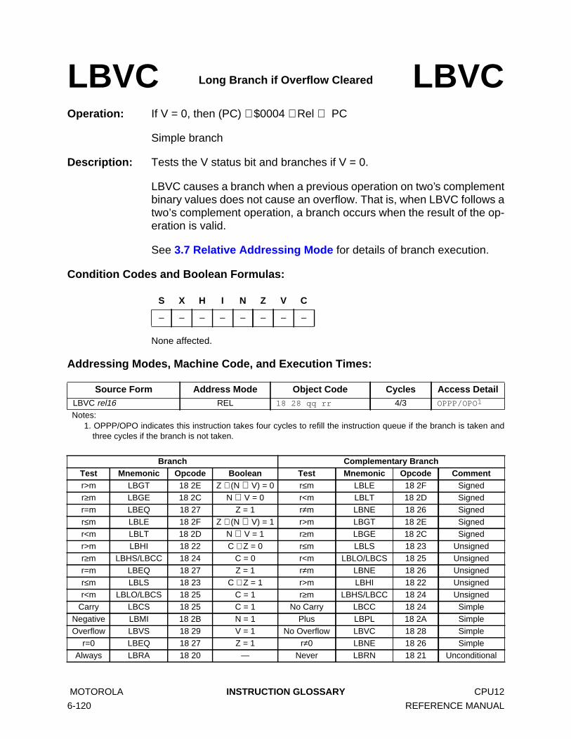
Operation: If V = 0, then (PC) + $0004 + Rel ⇒ PC
Simple branch
Description: Tests the V status bit and branches if V = 0.
LBVC causes a branch when a previous operation on two’s complementbinary values does not cause an overflow. That is, when LBVC follows atwo’s complement operation, a branch occurs when the result of the op-eration is valid.
See 3.7 Relative Addressing Mode for details of branch execution.
Condition Codes and Boolean Formulas:
None affected.
Addressing Modes, Machine Code, and Execution Times:
LBVC Long Branch if Overflow Cleared LBVC
S X H I N Z V C
– – – – – – – –
Source Form Address Mode Object Code Cycles Access DetailLBVC rel16 REL 18 28 qq rr 4/3 OPPP/OPO1
Notes:1. OPPP/OPO indicates this instruction takes four cycles to refill the instruction queue if the branch is taken and
three cycles if the branch is not taken.
Branch Complementary BranchTest Mnemonic Opcode Boolean Test Mnemonic Opcode Commentr>m LBGT 18 2E Z + (N ⊕ V) = 0 r≤m LBLE 18 2F Signedr≥m LBGE 18 2C N ⊕ V = 0 r<m LBLT 18 2D Signedr=m LBEQ 18 27 Z = 1 r≠m LBNE 18 26 Signedr≤m LBLE 18 2F Z + (N ⊕ V) = 1 r>m LBGT 18 2E Signedr<m LBLT 18 2D N ⊕ V = 1 r≥m LBGE 18 2C Signedr>m LBHI 18 22 C + Z = 0 r≤m LBLS 18 23 Unsignedr≥m LBHS/LBCC 18 24 C = 0 r<m LBLO/LBCS 18 25 Unsignedr=m LBEQ 18 27 Z = 1 r≠m LBNE 18 26 Unsignedr≤m LBLS 18 23 C + Z = 1 r>m LBHI 18 22 Unsignedr<m LBLO/LBCS 18 25 C = 1 r≥m LBHS/LBCC 18 24 Unsigned
Carry LBCS 18 25 C = 1 No Carry LBCC 18 24 SimpleNegative LBMI 18 2B N = 1 Plus LBPL 18 2A SimpleOverflow LBVS 18 29 V = 1 No Overflow LBVC 18 28 Simple
r=0 LBEQ 18 27 Z = 1 r≠0 LBNE 18 26 SimpleAlways LBRA 18 20 — Never LBRN 18 21 Unconditional
MOTOROLA INSTRUCTION GLOSSARY CPU12
6-120 REFERENCE MANUAL

Operation: If V = 1, then (PC) + $0004 + Rel ⇒ PC
Simple branch
Description: Tests the V status bit and branches if V = 1.
LBVS causes a branch when a previous operation on two’s complementbinary values causes an overflow. That is, when LBVS follows a two’scomplement operation, a branch occurs when the result of the operationis invalid.
See 3.7 Relative Addressing Mode for details of branch execution.
Condition Codes and Boolean Formulas:
None affected.
Addressing Modes, Machine Code, and Execution Times:
LBVS Long Branch if Overflow Set LBVS
S X H I N Z V C
– – – – – – – –
Source Form Address Mode Object Code Cycles Access DetailLBVS rel16 REL 18 29 qq rr 4/3 OPPP/OPO1
Notes:1. OPPP/OPO indicates this instruction takes four cycles to refill the instruction queue if the branch is taken and
three cycles if the branch is not taken.
Branch Complementary BranchTest Mnemonic Opcode Boolean Test Mnemonic Opcode Commentr>m LBGT 18 2E Z + (N ⊕ V) = 0 r≤m LBLE 18 2F Signedr≥m LBGE 18 2C N ⊕ V = 0 r<m LBLT 18 2D Signedr=m LBEQ 18 27 Z = 1 r≠m LBNE 18 26 Signedr≤m LBLE 18 2F Z + (N ⊕ V) = 1 r>m LBGT 18 2E Signedr<m LBLT 18 2D N ⊕ V = 1 r≥m LBGE 18 2C Signedr>m LBHI 18 22 C + Z = 0 r≤m LBLS 18 23 Unsignedr≥m LBHS/LBCC 18 24 C = 0 r<m LBLO/LBCS 18 25 Unsignedr=m LBEQ 18 27 Z = 1 r≠m LBNE 18 26 Unsignedr≤m LBLS 18 23 C + Z = 1 r>m LBHI 18 22 Unsignedr<m LBLO/LBCS 18 25 C = 1 r≥m LBHS/LBCC 18 24 Unsigned
Carry LBCS 18 25 C = 1 No Carry LBCC 18 24 SimpleNegative LBMI 18 2B N = 1 Plus LBPL 18 2A SimpleOverflow LBVS 18 29 V = 1 No Overflow LBVC 18 28 Simple
r=0 LBEQ 18 27 Z = 1 r≠0 LBNE 18 26 SimpleAlways LBRA 18 20 — Never LBRN 18 21 Unconditional
CPU12 INSTRUCTION GLOSSARY MOTOROLA
REFERENCE MANUAL 6-121

Operation: (M) ⇒ A
Description: Loads the content of memory location M into accumulator A. The condi-tion codes are set according to the data.
Condition Codes and Boolean Formulas:
Addressing Modes, Machine Code, and Execution Times:
LDAA Load Accumulator A LDAA
S X H I N Z V C
– – – – ∆ ∆ 0 –
N: Set if MSB of result is set; cleared otherwise.
Z: Set if result is $00; cleared otherwise.
V: 0; Cleared.
Source Form Address Mode Object Code Cycles Access DetailLDAA #opr8iLDAA opr8aLDAA opr16aLDAA oprx0_xyspLDAA oprx9,xyspLDAA oprx16,xyspLDAA [D,xysp]LDAA [oprx16,xysp]
IMMDIREXTIDXIDX1IDX2
[D,IDX][IDX2]
86 ii
96 dd
B6 hh ll
A6 xb
A6 xb ff
A6 xb ee ff
A6 xb
A6 xb ee ff
13333466
P
rfP
rOP
rfP
rPO
frPP
fIfrfP
fIPrfP
MOTOROLA INSTRUCTION GLOSSARY CPU12
6-122 REFERENCE MANUAL

Operation: (M) ⇒ B
Description: Loads the content of memory location M into accumulator B. The condi-tion codes are set according to the data.
Condition Codes and Boolean Formulas:
Addressing Modes, Machine Code, and Execution Times:
LDAB Load Accumulator B LDAB
S X H I N Z V C
– – – – ∆ ∆ 0 –
N: Set if MSB of result is set; cleared otherwise.
Z: Set if result is $00; cleared otherwise.
V: 0; Cleared.
Source Form Address Mode Object Code Cycles Access DetailLDAB #opr8iLDAB opr8aLDAB opr16aLDAB oprx0_xyspLDAB oprx9,xyspLDAB oprx16,xyspLDAB [D,xysp]LDAB [oprx16,xysp]
IMMDIREXTIDXIDX1IDX2
[D,IDX][IDX2]
C6 ii
D6 dd
F6 hh ll
E6 xb
E6 xb ff
E6 xb ee ff
E6 xb
E6 xb ee ff
13333466
P
rfP
rOP
rfP
rPO
frPP
fIfrfP
fIPrfP
CPU12 INSTRUCTION GLOSSARY MOTOROLA
REFERENCE MANUAL 6-123

Operation: (M : M + 1) ⇒ A : B
Description: Loads the contents of memory locations M and M+1 into double accu-mulator D. The condition codes are set according to the data. The infor-mation from M is loaded into accumulator A, and the information fromM+1 is loaded into accumulator B.
Condition Codes and Boolean Formulas:
Addressing Modes, Machine Code, and Execution Times:
LDD Load Double Accumulator LDD
S X H I N Z V C
– – – – ∆ ∆ 0 –
N: Set if MSB of result is set; cleared otherwise.
Z: Set if result is $0000; cleared otherwise.
V: 0; Cleared.
Source Form Address Mode Object Code Cycles Access DetailLDD #opr16iLDD opr8aLDD opr16aLDD oprx0_xyspLDD oprx9,xyspLDD oprx16,xyspLDD [D,xysp]LDD [oprx16,xysp]
IMMDIREXTIDXIDX1IDX2
[D,IDX][IDX2]
CC jj kk
DC dd
FC hh ll
EC xb
EC xb ff
EC xb ee ff
EC xb
EC xb ee ff
23333466
OP
RfP
ROP
RfP
RPO
fRPP
fIfRfP
fIPRfP
MOTOROLA INSTRUCTION GLOSSARY CPU12
6-124 REFERENCE MANUAL

Operation: (M : M+1) ⇒ SP
Description: Loads the most significant byte of the SP with the content of memory lo-cation M, and loads the least significant byte of the SP with the contentof the next byte of memory at M + 1.
Condition Codes and Boolean Formulas:
Addressing Modes, Machine Code, and Execution Times:
LDS Load Stack Pointer LDS
S X H I N Z V C
– – – – ∆ ∆ 0 –
N: Set if MSB of result is set; cleared otherwise.
Z: Set if result is $0000; cleared otherwise.
V: 0; Cleared.
Source Form Address Mode Object Code Cycles Access DetailLDS #opr16iLDS opr8aLDS opr16aLDS oprx0_xyspLDS oprx9,xyspLDS oprx16,xyspLDS [D,xysp]LDS [oprx16,xysp]
IMMDIREXTIDXIDX1IDX2
[D,IDX][IDX2]
CF jj kk
DF dd
FF hh ll
EF xb
EF xb ff
EF xb ee ff
EF xb
EF xb ee ff
23333466
OP
RfP
ROP
RfP
RPO
fRPP
fIfRfP
fIPRfP
CPU12 INSTRUCTION GLOSSARY MOTOROLA
REFERENCE MANUAL 6-125
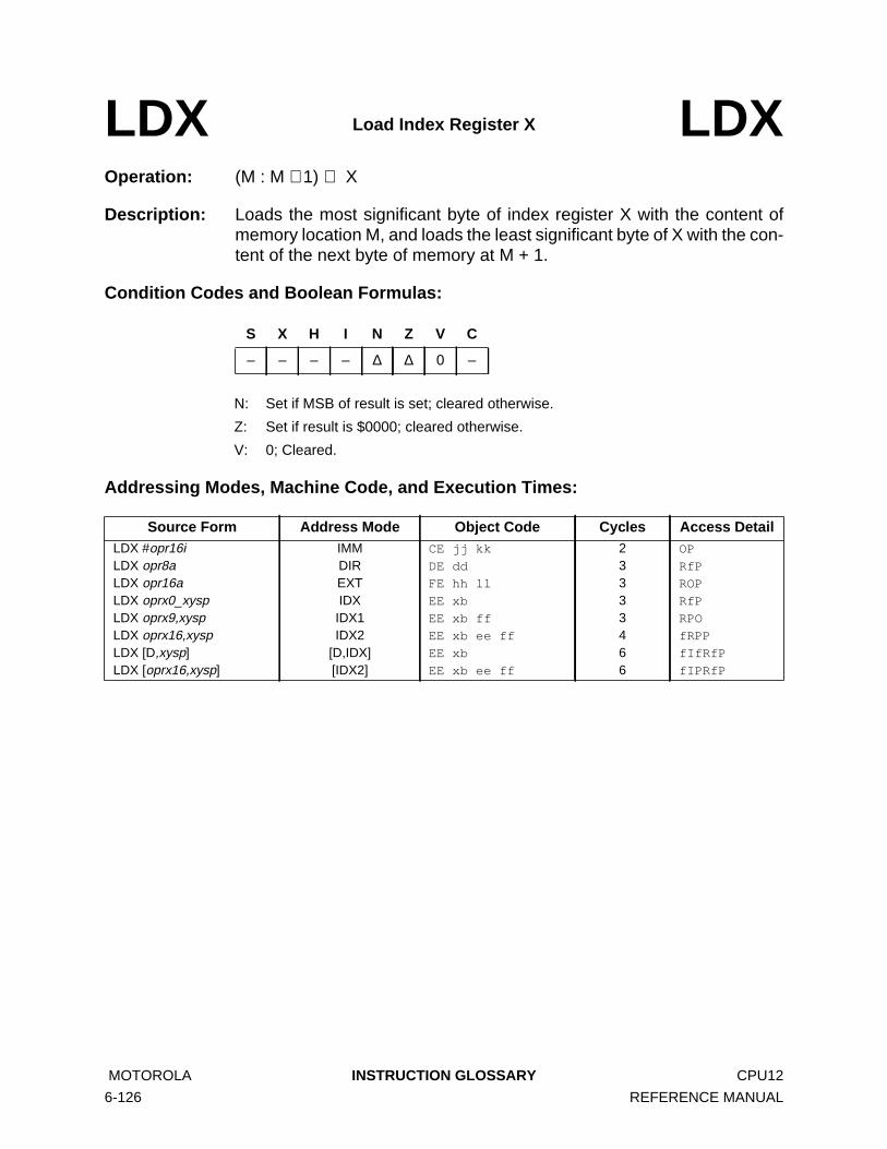
Operation: (M : M + 1) ⇒ X
Description: Loads the most significant byte of index register X with the content ofmemory location M, and loads the least significant byte of X with the con-tent of the next byte of memory at M + 1.
Condition Codes and Boolean Formulas:
Addressing Modes, Machine Code, and Execution Times:
LDX Load Index Register X LDX
S X H I N Z V C
– – – – ∆ ∆ 0 –
N: Set if MSB of result is set; cleared otherwise.
Z: Set if result is $0000; cleared otherwise.
V: 0; Cleared.
Source Form Address Mode Object Code Cycles Access DetailLDX #opr16iLDX opr8aLDX opr16aLDX oprx0_xyspLDX oprx9,xyspLDX oprx16,xyspLDX [D,xysp]LDX [oprx16,xysp]
IMMDIREXTIDXIDX1IDX2
[D,IDX][IDX2]
CE jj kk
DE dd
FE hh ll
EE xb
EE xb ff
EE xb ee ff
EE xb
EE xb ee ff
23333466
OP
RfP
ROP
RfP
RPO
fRPP
fIfRfP
fIPRfP
MOTOROLA INSTRUCTION GLOSSARY CPU12
6-126 REFERENCE MANUAL

Operation: (M : M + 1) ⇒ Y
Description: Loads the most significant byte of index register Y with the content ofmemory location M, and loads the least significant byte of Y with the con-tent of the next memory location at M + 1.
Condition Codes and Boolean Formulas:
Addressing Modes, Machine Code, and Execution Times:
LDY Load Index Register Y LDY
S X H I N Z V C
– – – – ∆ ∆ 0 –
N: Set if MSB of result is set; cleared otherwise.
Z: Set if result is $0000; cleared otherwise.
V: 0; Cleared.
Source Form Address Mode Object Code Cycles Access DetailLDY #opr16iLDY opr8aLDY opr16aLDY oprx0_xyspLDY oprx9,xyspLDY oprx16,xyspLDY [D,xysp]LDY [oprx16,xysp]
IMMDIREXTIDXIDX1IDX2
[D,IDX][IDX2]
CD jj kk
DD dd
FD hh ll
ED xb
ED xb ff
ED xb ee ff
ED xb
ED xb ee ff
23333466
OP
RfP
ROP
RfP
RPO
fRPP
fIfRfP
fIPRfP
CPU12 INSTRUCTION GLOSSARY MOTOROLA
REFERENCE MANUAL 6-127

Operation: Effective Address ⇒ SP
Description: Loads the stack pointer with an effective address specified by the pro-gram. The effective address can be any indexed addressing mode oper-and address except an indirect address. Indexed addressing modeoperand addresses are formed by adding an optional constant suppliedby the program or an accumulator value to the current value in X, Y, SP,or PC. See 3.8 Indexed Addressing Modes for more details.
LEAS does not alter condition code bits. This allows stack modificationwithout disturbing CCR bits changed by recent arithmetic operations.
Operation is a bit more complex when LEAS is used with auto-incrementor aut-odecrement operand specifications and the SP is the referencedindex register. The index register is loaded with what would have goneout to the address bus in the case of a load index instruction. In the caseof a pre-increment or pre-decrement, the modification is made before theindex register is loaded. In the case of a post-increment or post-decre-ment, modification would have taken effect after the address went out onthe address bus, so post-modification does not affect the content of theindex register.
Condition Codes and Boolean Formulas:
None affected.
Addressing Modes, Machine Code, and Execution Times:
LEAS Load Stack Pointer withEffective Address LEAS
S X H I N Z V C
– – – – – – – –
Source Form Address Mode Object Code Cycles Access DetailLEAS oprx0_xyspLEAS oprx9,xyspLEAS oprx16,xysp
IDXIDX1IDX2
1B xb
1B xb ff
1B xb ee ff
222
PP1
PO
PP
Notes:1. Due to internal CPU requirements, the program word fetch is performed twice to the same address during this
instruction.
MOTOROLA INSTRUCTION GLOSSARY CPU12
6-128 REFERENCE MANUAL

Operation: Effective Address ⇒ X
Description: Loads index register X with an effective address specified by the pro-gram. The effective address can be any indexed addressing mode oper-and address except an indirect address. Indexed addressing modeoperand addresses are formed by adding an optional constant suppliedby the program or an accumulator value to the current value in X, Y, SP,or PC. See 3.8 Indexed Addressing Modes for more details.
Operation is a bit more complex when LEAX is used with auto-incrementor auto-decrement operand specifications and index register X is the ref-erenced index register. The index register is loaded with what wouldhave gone out to the address bus in the case of a load indexed instruc-tion. In the case of a pre-increment or pre-decrement, the modification ismade before the index register is loaded. In the case of a post-incrementor post-decrement, modification would have taken effect after the ad-dress went out on the address bus, so post-modification does not affectthe content of the index register.
Condition Codes and Boolean Formulas:
None affected.
Addressing Modes, Machine Code, and Execution Times:
LEAX Load X with Effective Address LEAX
S X H I N Z V C
– – – – – – – –
Source Form Address Mode Object Code Cycles Access DetailLEAX oprx0_xyspLEAX oprx9,xyspLEAX oprx16,xysp
IDXIDX1IDX2
1A xb
1A xb ff
1A xb ee ff
222
PP1
PO
PP
Notes:1. Due to internal CPU requirements, the program word fetch is performed twice to the same address during this
instruction.
CPU12 INSTRUCTION GLOSSARY MOTOROLA
REFERENCE MANUAL 6-129

Operation: Effective Address ⇒ Y
Description: Loads index register Y with an effective address specified by the pro-gram. The effective address can be any indexed addressing mode oper-and address except an indirect address. Indexed addressing modeoperand addresses are formed by adding an optional constant suppliedby the program or an accumulator value to the current value in X, Y, SP,or PC. See 3.8 Indexed Addressing Modes for more details.
Operation is a bit more complex when LEAY is used with auto-incrementor auto-decrement operand specifications and index register Y is the ref-erenced index register. The index register is loaded with what wouldhave gone out to the address bus in the case of a load indexed instruc-tion. In the case of a pre-increment or pre-decrement, the modification ismade before the index register is loaded. In the case of a post-incrementor post-decrement, modification would have taken effect after the ad-dress went out on the address bus, so post-modification does not affectthe content of the index register.
Condition Codes and Boolean Formulas:
None affected.
Addressing Modes, Machine Code, and Execution Times:
LEAY Load Y with Effective Address LEAY
S X H I N Z V C
– – – – – – – –
Source Form Address Mode Object Code Cycles Access DetailLEAY oprx0_xyspLEAY oprx9,xyspLEAY oprx16,xysp
IDXIDX1IDX2
19 xb
19 xb ff
19 xb ee ff
222
PP1
PO
PP
Notes:1. Due to internal CPU requirements, the program word fetch is performed twice to the same address during this
instruction.
MOTOROLA INSTRUCTION GLOSSARY CPU12
6-130 REFERENCE MANUAL

Operation:
Description: Shifts all bits of the memory location M one place to the left. Bit 0 is load-ed with zero. The C status bit is loaded from the most significant bit of M.
Condition Codes and Boolean Formulas:
Addressing Modes, Machine Code, and Execution Times:
LSL Logical Shift Left Memory(Same as ASL) LSL
S X H I N Z V C
– – – – ∆ ∆ ∆ ∆
N: Set if MSB of result is set; cleared otherwise.
Z: Set if result is $00; cleared otherwise.
V: N ⊕ C = [N • C] + [N • C] (for N and C after the shift)Set if (N is set and C is cleared) or (N is cleared and C is set); cleared oth-erwise (for values of N and C after the shift).
C: M7Set if the LSB of M was set before the shift; cleared otherwise.
Source Form Address Mode Object Code Cycles Access DetailLSL opr16aLSL oprx0_xyspLSL oprx9,xyspLSL oprx16,xyspLSL [D,xysp]LSL [oprx16,xysp]
EXTIDXIDX1IDX2
[D,IDX][IDX2]
78 hh ll
68 xb
68 xb ff
68 xb ee ff
68 xb
68 xb ee ff
434566
rOPw
rPw
rPOw
frPPw
fIfrPw
fIPrPw
b7 – – – – – – b0C 0
CPU12 INSTRUCTION GLOSSARY MOTOROLA
REFERENCE MANUAL 6-131

Operation:
Description: Shifts all bits of accumulator A one place to the left. Bit 0 is loaded withzero. The C status bit is loaded from the most significant bit of A.
Condition Codes and Boolean Formulas:
Addressing Modes, Machine Code, and Execution Times:
LSLA Logical Shift Left A(Same as ASLA) LSLA
S X H I N Z V C
– – – – ∆ ∆ ∆ ∆
N: Set if MSB of result is set; cleared otherwise.
Z: Set if result is $00; cleared otherwise.
V: N ⊕ C = [N • C] + [N • C] (for N and C after the shift)Set if (N is set and C is cleared) or (N is cleared and C is set); cleared oth-erwise (for values of N and C after the shift).
C: A7Set if the LSB of A was set before the shift; cleared otherwise.
Source Form Address Mode Object Code Cycles Access DetailLSLA INH 48 1 O
b7 – – – – – – b0C 0
MOTOROLA INSTRUCTION GLOSSARY CPU12
6-132 REFERENCE MANUAL

Operation:
Description: Shifts all bits of accumulator B one place to the left. Bit 0 is loaded withzero. The C status bit is loaded from the most significant bit of B.
Condition Codes and Boolean Formulas:
Addressing Modes, Machine Code, and Execution Times:
LSLB Logical Shift Left B(Same as ASLB) LSLB
S X H I N Z V C
– – – – ∆ ∆ ∆ ∆
N: Set if MSB of result is set; cleared otherwise.
Z: Set if result is $00; cleared otherwise.
V: N ⊕ C = [N • C] + [N • C] (for N and C after the shift)Set if (N is set and C is cleared) or (N is cleared and C is set); cleared oth-erwise (for values of N and C after the shift).
C: B7Set if the LSB of B was set before the shift; cleared otherwise.
Source Form Address Mode Object Code Cycles Access DetailLSLB INH 58 1 O
b7 – – – – – – b0C 0
CPU12 INSTRUCTION GLOSSARY MOTOROLA
REFERENCE MANUAL 6-133
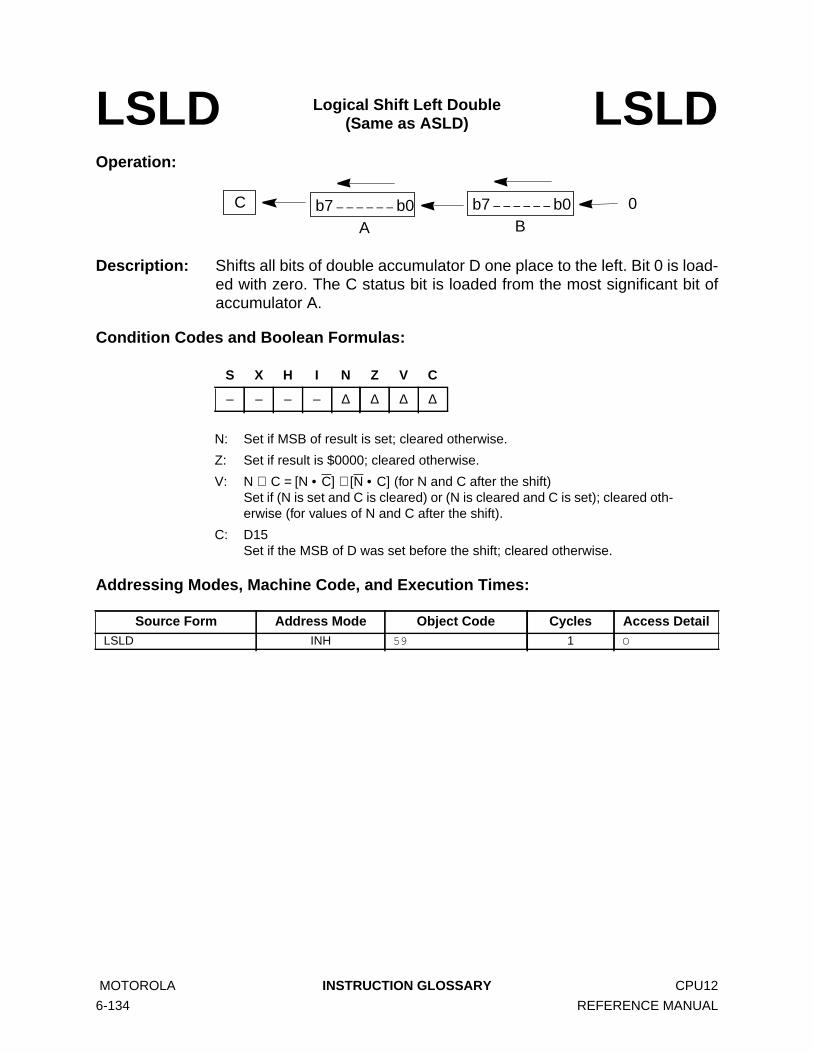
Operation:
Description: Shifts all bits of double accumulator D one place to the left. Bit 0 is load-ed with zero. The C status bit is loaded from the most significant bit ofaccumulator A.
Condition Codes and Boolean Formulas:
Addressing Modes, Machine Code, and Execution Times:
LSLD Logical Shift Left Double(Same as ASLD) LSLD
S X H I N Z V C
– – – – ∆ ∆ ∆ ∆
N: Set if MSB of result is set; cleared otherwise.
Z: Set if result is $0000; cleared otherwise.
V: N ⊕ C = [N • C] + [N • C] (for N and C after the shift)Set if (N is set and C is cleared) or (N is cleared and C is set); cleared oth-erwise (for values of N and C after the shift).
C: D15Set if the MSB of D was set before the shift; cleared otherwise.
Source Form Address Mode Object Code Cycles Access DetailLSLD INH 59 1 O
b7 – – – – – – b0 C 0 b7 – – – – – – b0
A B
MOTOROLA INSTRUCTION GLOSSARY CPU12
6-134 REFERENCE MANUAL

Operation:
Description: Shifts all bits of memory location M one place to the right. Bit 7 is loadedwith zero. The C status bit is loaded from the least significant bit of M.
Condition Codes and Boolean Formulas:
Addressing Modes, Machine Code, and Execution Times:
LSR Logical Shift Right Memory LSR
S X H I N Z V C
– – – – 0 ∆ ∆ ∆
N: 0; Cleared.
Z: Set if result is $00; cleared otherwise.
V: N ⊕ C = [N • C] + [N • C] (for N and C after the shift)Set if (N is set and C is cleared) or (N is cleared and C is set); cleared oth-erwise (for values of N and C after the shift).
C: M0Set if the LSB of M was set before the shift; cleared otherwise.
Source Form Address Mode Object Code Cycles Access DetailLSR opr16aLSR oprx0_xyspLSR oprx9,xyspLSR oprx16,xyspLSR [D,xysp]LSR [oprx16,xysp]
EXTIDXIDX1IDX2
[D,IDX][IDX2]
74 hh ll
64 xb
64 xb ff
64 xb ee ff
64 xb
64 xb ee ff
434566
rOPw
rPw
rPOw
frPPw
fIfrPw
fIPrPw
b7 – – – – – – b0 C0
CPU12 INSTRUCTION GLOSSARY MOTOROLA
REFERENCE MANUAL 6-135

Operation:
Description: Shifts all bits of accumulator A one place to the right. Bit 7 is loaded withzero. The C status bit is loaded from the least significant bit of A.
Condition Codes and Boolean Formulas:
Addressing Modes, Machine Code, and Execution Times:
LSRA Logical Shift Right A LSRA
S X H I N Z V C
– – – – 0 ∆ ∆ ∆
N: 0; Cleared.
Z: Set if result is $00; cleared otherwise.
V: N ⊕ C = [N • C] + [N • C] (for N and C after the shift)Set if (N is set and C is cleared) or (N is cleared and C is set); cleared oth-erwise (for values of N and C after the shift).
C: A0Set if the LSB of A was set before the shift; cleared otherwise.
Source Form Address Mode Object Code Cycles Access DetailLSRA INH 44 1 O
b7 – – – – – – b0 C0
MOTOROLA INSTRUCTION GLOSSARY CPU12
6-136 REFERENCE MANUAL

Operation:
Description: Shifts all bits of accumulator B one place to the right. Bit 7 is loaded withzero. The C status bit is loaded from the least significant bit of B.
Condition Codes and Boolean Formulas:
Addressing Modes, Machine Code, and Execution Times:
LSRB Logical Shift Right B LSRB
S X H I N Z V C
– – – – 0 ∆ ∆ ∆
N: 0; Cleared.
Z: Set if result is $00; cleared otherwise.
V: N ⊕ C = [N • C] + [N • C] (for N and C after the shift)Set if (N is set and C is cleared) or (N is cleared and C is set); cleared oth-erwise (for values of N and C after the shift).
C: B0Set if the LSB of B was set before the shift; cleared otherwise.
Source Form Address Mode Object Code Cycles Access DetailLSRB INH 54 1 O
b7 – – – – – – b0 C0
CPU12 INSTRUCTION GLOSSARY MOTOROLA
REFERENCE MANUAL 6-137
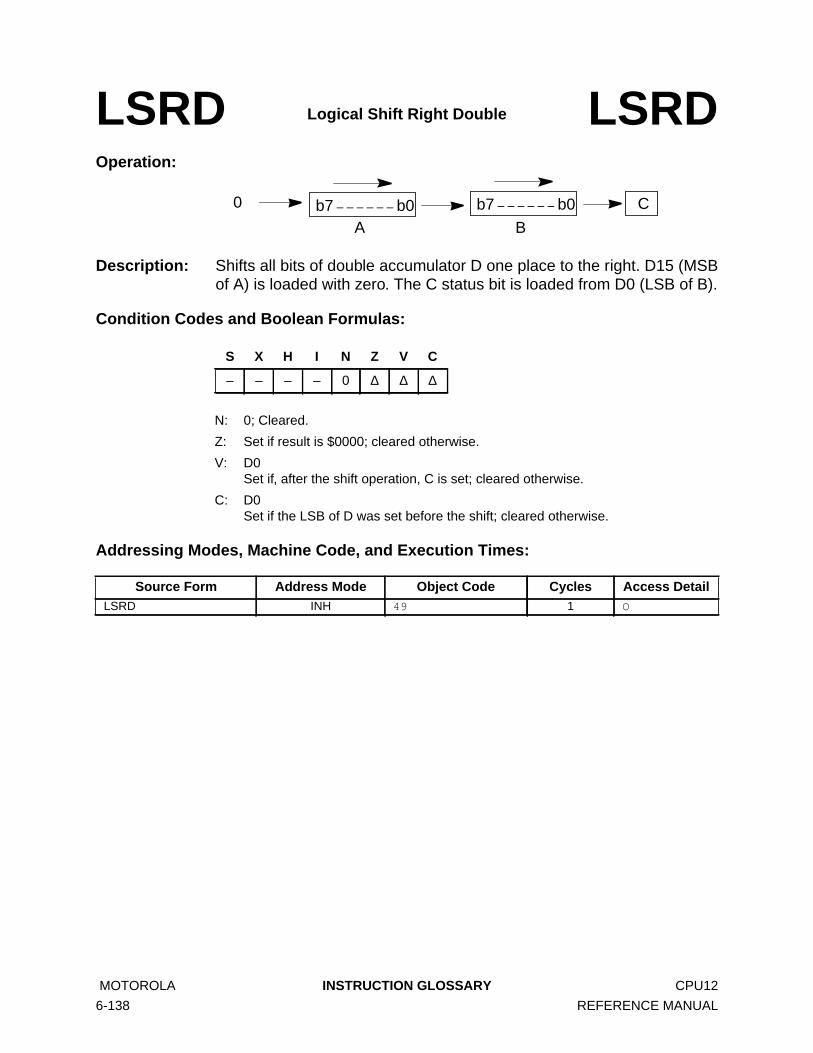
Operation:
Description: Shifts all bits of double accumulator D one place to the right. D15 (MSBof A) is loaded with zero. The C status bit is loaded from D0 (LSB of B).
Condition Codes and Boolean Formulas:
Addressing Modes, Machine Code, and Execution Times:
LSRD Logical Shift Right Double LSRD
S X H I N Z V C
– – – – 0 ∆ ∆ ∆
N: 0; Cleared.
Z: Set if result is $0000; cleared otherwise.
V: D0Set if, after the shift operation, C is set; cleared otherwise.
C: D0Set if the LSB of D was set before the shift; cleared otherwise.
Source Form Address Mode Object Code Cycles Access DetailLSRD INH 49 1 O
b7 – – – – – – b0 0 C b7 – – – – – – b0
A B
MOTOROLA INSTRUCTION GLOSSARY CPU12
6-138 REFERENCE MANUAL

Operation: MAX ((A), (M)) ⇒ A
Description: Subtracts an unsigned 8-bit value in memory from an unsigned 8-bitvalue in accumulator A to determine which is larger, and leaves the larg-er of the two values in A. The Z status bit is set when the result of thesubtraction is zero (the values are equal), and the C status bit is set whenthe subtraction requires a borrow (the value in memory is larger than thevalue in the accumulator). When C = 1, the value in A has been replacedby the value in memory.
The unsigned value in memory is accessed by means of indexed ad-dressing modes, which allow a great deal of flexibility in specifying theaddress of the operand. Auto increment/decrement variations of indexedaddressing facilitate finding the largest value in a list of values.
Condition Codes and Boolean Formulas:
Addressing Modes, Machine Code, and Execution Times:
MAXA Place Larger of TwoUnsigned 8-Bit Values
in Accumulator AMAXA
S X H I N Z V C
– – – – ∆ ∆ ∆ ∆
N: Set if MSB of result is set; cleared otherwise.
Z: Set if result is $00; cleared otherwise.
V: X7 • M7 • R7 + X7 • M7 • R7Set if a two’s complement overflow resulted from the operation;cleared otherwise.
C: X7 • M7 + M7 • R7 + R7 • X7Set if the value of the content of memory is larger than the value ofthe accumulator; cleared otherwise.
Condition codes reflect internal subtraction (R = A – M).
Source Form Address Mode Object Code Cycles Access DetailMAXA oprx0_xyspMAXA oprx9,xyspMAXA oprx16,xyspMAXA [D,xysp]MAXA [oprx16,xysp]
IDXIDX1IDX2
[D,IDX][IDX2]
18 18 xb
18 18 xb ff
18 18 xb ee ff
18 18 xb
18 18 xb ee ff
44577
OrfP
OrPO
OfrPP
OfIfrfP
OfIPrfP
CPU12 INSTRUCTION GLOSSARY MOTOROLA
REFERENCE MANUAL 6-139

Operation: MAX ((A), (M)) ⇒ M
Description: Subtracts an unsigned 8-bit value in memory from an unsigned 8-bitvalue in accumulator A to determine which is larger, and leaves the larg-er of the two values in the memory location. The Z status bit is set whenthe result of the subtraction is zero (the values are equal), and the C sta-tus bit is set when the subtraction requires a borrow (the value in mem-ory is larger than the value in the accumulator). When C = 0, the valuein accumulator A has replaced the value in memory.
The unsigned value in memory is accessed by means of indexed ad-dressing modes, which allow a great deal of flexibility in specifying theaddress of the operand.
Condition Codes and Boolean Formulas:
Addressing Modes, Machine Code, and Execution Times:
MAXM Place Larger of TwoUnsigned 8-Bit Values
in MemoryMAXM
S X H I N Z V C
– – – – ∆ ∆ ∆ ∆
N: Set if MSB of result is set; cleared otherwise.
Z: Set if result is $00; cleared otherwise.
V: X7 • M7 • R7 + X7 • M7 • R7Set if a two’s complement overflow resulted from the operation;cleared otherwise.
C: X7 • M7 + M7 • R7 + R7 • X7Set if the value of the content of memory is larger than the value ofthe accumulator; cleared otherwise.
Condition codes reflect internal subtraction (R = A – M).
Source Form Address Mode Object Code Cycles Access DetailMAXM oprx0_xyspMAXM oprx9,xyspMAXM oprx16,xyspMAXM [D,xysp]MAXM [oprx16,xysp]
IDXIDX1IDX2
[D,IDX][IDX2]
18 1C xb
18 1C xb ff
18 1C xb ee ff
18 1C xb
18 1C xb ee ff
45677
OrPw
OrPwO
OfrPwP
OfIfrPw
OfIPrPw
MOTOROLA INSTRUCTION GLOSSARY CPU12
6-140 REFERENCE MANUAL
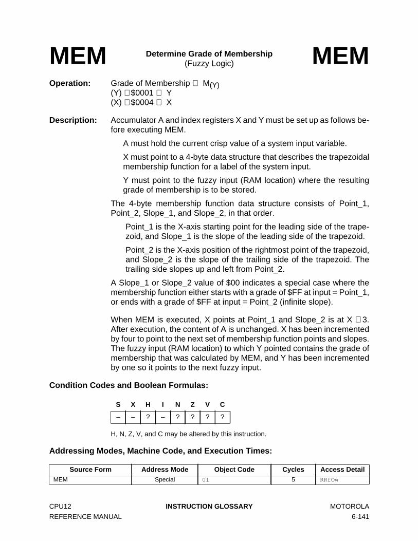
Operation: Grade of Membership ⇒ M(Y)(Y) + $0001 ⇒ Y(X) + $0004 ⇒ X
Description: Accumulator A and index registers X and Y must be set up as follows be-fore executing MEM.
A must hold the current crisp value of a system input variable.
X must point to a 4-byte data structure that describes the trapezoidalmembership function for a label of the system input.
Y must point to the fuzzy input (RAM location) where the resultinggrade of membership is to be stored.
The 4-byte membership function data structure consists of Point_1,Point_2, Slope_1, and Slope_2, in that order.
Point_1 is the X-axis starting point for the leading side of the trape-zoid, and Slope_1 is the slope of the leading side of the trapezoid.
Point_2 is the X-axis position of the rightmost point of the trapezoid,and Slope_2 is the slope of the trailing side of the trapezoid. Thetrailing side slopes up and left from Point_2.
A Slope_1 or Slope_2 value of $00 indicates a special case where themembership function either starts with a grade of $FF at input = Point_1,or ends with a grade of $FF at input = Point_2 (infinite slope).
When MEM is executed, X points at Point_1 and Slope_2 is at X + 3.After execution, the content of A is unchanged. X has been incrementedby four to point to the next set of membership function points and slopes.The fuzzy input (RAM location) to which Y pointed contains the grade ofmembership that was calculated by MEM, and Y has been incrementedby one so it points to the next fuzzy input.
Condition Codes and Boolean Formulas:
H, N, Z, V, and C may be altered by this instruction.
Addressing Modes, Machine Code, and Execution Times:
MEM Determine Grade of Membership(Fuzzy Logic) MEM
S X H I N Z V C
– – ? – ? ? ? ?
Source Form Address Mode Object Code Cycles Access DetailMEM Special 01 5 RRfOw
CPU12 INSTRUCTION GLOSSARY MOTOROLA
REFERENCE MANUAL 6-141

Operation: MIN ((A), (M)) ⇒ A
Description: Subtracts an unsigned 8-bit value in memory from an unsigned 8-bitvalue in accumulator A to determine which is larger, and leaves thesmaller of the two values in accumulator A. The Z status bit is set whenthe result of the subtraction is zero (the values are equal), and the C sta-tus bit is set when the subtraction requires a borrow (the value in mem-ory is larger than the value in the accumulator). When C = 0, the valuein accumulator A has been replaced by the value in memory.
The unsigned value in memory is accessed by means of indexed ad-dressing modes, which allow a great deal of flexibility in specifying theaddress of the operand. Auto increment/decrement variations of indexedaddressing facilitate finding the largest value in a list of values.
Condition Codes and Boolean Formulas:
Addressing Modes, Machine Code, and Execution Times:
MINA Place Smaller of TwoUnsigned 8-Bit Values
in Accumulator AMINA
S X H I N Z V C
– – – – ∆ ∆ ∆ ∆
N: Set if MSB of result is set; cleared otherwise.
Z: Set if result is $00; cleared otherwise.
V: X7 • M7 • R7 + X7 • M7 • R7Set if a two’s complement overflow resulted from the operation;cleared otherwise.
C: X7 • M7 + M7 • R7 + R7 • X7Set if the value of the content of memory is larger than the value ofthe accumulator; cleared otherwise.
Condition codes reflect internal subtraction (R = A – M).
Source Form Address Mode Object Code Cycles Access DetailMINA oprx0_xyspMINA oprx9,xyspMINA oprx16,xyspMINA [D,xysp]MINA [oprx16,xysp]
IDXIDX1IDX2
[D,IDX][IDX2]
18 19 xb
18 19 xb ff
18 19 xb ee ff
18 19 xb
18 19 xb ee ff
44577
OrfP
OrPO
OfrPP
OfIfrfP
OfIPrfP
MOTOROLA INSTRUCTION GLOSSARY CPU12
6-142 REFERENCE MANUAL

Operation: MIN ((A), (M)) ⇒ M
Description: Subtracts an unsigned 8-bit value in memory from an unsigned 8-bitvalue in accumulator A to determine which is larger, and leaves thesmaller of the two values in the memory location. The Z status bit is setwhen the result of the subtraction is zero (the values are equal), and theC status bit is set when the subtraction requires a borrow (the value inmemory is larger than the value in the accumulator). When C = 1, thevalue in accumulator A has replaced the value in memory.
The unsigned value in memory is accessed by means of indexed ad-dressing modes, which allow a great deal of flexibility in specifying theaddress of the operand.
Condition Codes and Boolean Formulas:
Addressing Modes, Machine Code, and Execution Times:
MINM Place Smaller of TwoUnsigned 8-Bit Values
in MemoryMINM
S X H I N Z V C
– – – – ∆ ∆ ∆ ∆
N: Set if MSB of result is set; cleared otherwise.
Z: Set if result is $00; cleared otherwise.
V: X7 • M7 • R7 + X7 • M7 • R7Set if a two’s complement overflow resulted from the operation;cleared otherwise.
C: X7 • M7 + M7 • R7 + R7 • X7Set if the value of the content of memory is larger than the value ofthe accumulator; cleared otherwise.
Condition codes reflect internal subtraction (R = A – M).
Source Form Address Mode Object Code Cycles Access DetailMINM oprx0_xyspMINM oprx9,xyspMINM oprx16,xyspMINM [D,xysp]MINM [oprx16,xysp]
IDXIDX1IDX2
[D,IDX][IDX2]
18 1D xb
18 1D xb ff
18 1D xb ee ff
18 1D xb
18 1D xb ee ff
45677
OrPw
OrPwO
OfrPwP
OfIfrPw
OfIPrPw
CPU12 INSTRUCTION GLOSSARY MOTOROLA
REFERENCE MANUAL 6-143

Operation: (M1) ⇒ M2
Description: Moves the content of one memory location to another memory location.The content of the source memory location is not changed.
Move instructions use separate addressing modes to access the sourceand destination of a move. The following combinations of addressingmodes are supported: IMM–EXT, IMM–IDX, EXT–EXT, EXT–IDX, IDX–EXT, and IDX–IDX. IDX operands allow indexed addressing mode spec-ifications that fit in a single postbyte; including 5-bit constant, accumula-tor offsets, and auto increment/decrement modes. Nine-bit and 16-bitconstant offsets would require additional extension bytes and are not al-lowed. Indexed indirect modes (for example [D,r]) are also not allowed.
There are special considerations when using PC-relative addressingwith move instructions. These are discussed in 3.9 Instructions UsingMultiple Modes .
Condition Codes and Boolean Formulas:
None affected.
Addressing Modes, Machine Code, and Execution Times:
MOVB Move a Byte of Datafrom One Memory Location to Another MOVB
S X H I N Z V C
– – – – – – – –
Source Form 1
Notes:1. The first operand in the source code statement specifies the source for the move.
Address Mode Object Code Cycles Access DetailMOVB #opr8, opr16aMOVB #opr8i, oprx0_xyspMOVB opr16a, opr16aMOVB opr16a, oprx0_xyspMOVB oprx0_xysp, opr16aMOVB oprx0_xysp, oprx0_xysp
IMM–EXTIMM–IDXEXT–EXTEXT–IDXIDX–EXTIDX–IDX
18 0B ii hh ll
18 08 xb ii
18 0C hh ll hh ll
18 09 xb hh ll
18 0D xb hh ll
18 0A xb xb
446555
OPwP
OPwO
OrPwPO
OPrPw
OrPwP
OrPwO
MOTOROLA INSTRUCTION GLOSSARY CPU12
6-144 REFERENCE MANUAL

Operation: (M : M + 11) ⇒ M : M + 12
Description: Moves the content of one location in memory to another location in mem-ory. The content of the source memory location is not changed.
Move instructions use separate addressing modes to access the sourceand destination of a move. The following combinations of addressingmodes are supported: IMM–EXT, IMM–IDX, EXT–EXT, EXT–IDX, IDX–EXT, and IDX–IDX. IDX operands allow indexed addressing mode spec-ifications that fit in a single postbyte; including 5-bit constant, accumula-tor offsets, and auto increment/decrement modes. Nine-bit and 16-bitconstant offsets would require additional extension bytes and are not al-lowed. Indexed indirect modes (for example [D,r]) are also not allowed.
There are special considerations when using PC-relative addressingwith move instructions. These are discussed in 3.9 Instructions UsingMultiple Modes .
Condition Codes and Boolean Formulas:
None affected.
Addressing Modes, Machine Code, and Execution Times:
MOVW Move a Word of Datafrom One Memory Location to Another MOVW
S X H I N Z V C
– – – – – – – –
Source Form 1
Notes:1. The first operand in the source code statement specifies the source for the move.
Address Mode Object Code Cycles Access DetailMOVW #opr16i, opr16aMOVW #opr16i, oprx0_xyspMOVW opr16a, opr16aMOVW opr16a, oprx0_xyspMOVW oprx0_xysp, opr16aMOVW oprx0_xysp, oprx0_xysp
IMM–EXTIMM–IDXEXT–EXTEXT–IDXIDX–EXTIDX–IDX
18 03 jj kk hh ll
18 00 xb jj kk
18 04 hh ll hh ll
18 01 xb hh ll
18 05 xb hh ll
18 02 xb xb
546555
OPWPO
OPPW
ORPWPO
OPRPW
ORPWP
ORPWO
CPU12 INSTRUCTION GLOSSARY MOTOROLA
REFERENCE MANUAL 6-145

Operation: (A) × (B) ⇒ A : B
Description: Multiplies the 8-bit unsigned binary value in accumulator A by the 8-bitunsigned binary value in accumulator B, and places the 16-bit unsignedresult in double accumulator D. The carry flag allows rounding the mostsignificant byte of the result through the sequence: MUL, ADCA #0.
Condition Codes and Boolean Formulas:
Addressing Modes, Machine Code, and Execution Times:
MUL Multiply8-Bit by 8-Bit (Unsigned) MUL
S X H I N Z V C
– – – – – – – ∆
C: R7Set if bit 7 of the result (B bit 7) is set; cleared otherwise.
Source Form Address Mode Object Code Cycles Access DetailMUL INH 12 3 ffO
MOTOROLA INSTRUCTION GLOSSARY CPU12
6-146 REFERENCE MANUAL

Operation: 0 – (M) = (M) + 1 ⇒ M
Description: Replaces the content of memory location M with its two’s complement(the value $80 is left unchanged).
Condition Codes and Boolean Formulas:
Addressing Modes, Machine Code, and Execution Times:
NEG Negate Memory NEG
S X H I N Z V C
– – – – ∆ ∆ ∆ ∆
N: Set if MSB of result is set; cleared otherwise.
Z: Set if result is $00; cleared otherwise.
V: R7 • R6 • R5 • R4 • R3 • R2 • R1 • R0Set if there is a two’s complement overflow from the implied subtractionfrom zero; cleared otherwise. Two’s complement overflow occurs if andonly if (M) = $80
C: R7 + R6 + R5 + R4 + R3 + R2 + R1 + R0Set if there is a borrow in the implied subtraction from zero; cleared oth-erwise. Set in all cases except when (M) = $00.
Source Form Address Mode Object Code Cycles Access DetailNEG opr16aNEG oprx0_xyspNEG oprx9,xyspNEG oprx16,xyspNEG [D,xysp]NEG [oprx16,xysp]
EXTIDXIDX1IDX2
[D,IDX][IDX2]
70 hh ll
60 xb
60 xb ff
60 xb ee ff
60 xb
60 xb ee ff
434566
rOPw
rPw
rPOw
frPPw
fIfrPw
fIPrPw
CPU12 INSTRUCTION GLOSSARY MOTOROLA
REFERENCE MANUAL 6-147

Operation: 0 – (A) = (A) + 1 ⇒ A
Description: Replaces the content of accumulator A with its two’s complement (thevalue $80 is left unchanged).
Condition Codes and Boolean Formulas:
Addressing Modes, Machine Code, and Execution Times:
NEGA Negate A NEGA
S X H I N Z V C
– – – – ∆ ∆ ∆ ∆
N: Set if MSB of result is set; cleared otherwise.
Z: Set if result is $00; cleared otherwise.
V: R7 • R6 • R5 • R4 • R3 • R2 • R1 • R0Set if there is a two’s complement overflow from the implied subtractionfrom zero; cleared otherwise. Two’s complement overflow occurs ifand only if (A) = $80.
C: R7 + R6 + R5 + R4 + R3 + R2 + R1 + R0Set if there is a borrow in the implied subtraction from zero; cleared oth-erwise. Set in all cases except when (A) = $00.
Source Form Address Mode Object Code Cycles Access DetailNEGA INH 40 1 O
MOTOROLA INSTRUCTION GLOSSARY CPU12
6-148 REFERENCE MANUAL

Operation: 0 – (B) = (B) + 1 ⇒ B
Description: Replaces the content of accumulator B with its two’s complement (thevalue $80 is left unchanged).
Condition Codes and Boolean Formulas:
Addressing Modes, Machine Code, and Execution Times:
NEGB Negate B NEGB
S X H I N Z V C
– – – – ∆ ∆ ∆ ∆
N: Set if MSB of result is set; cleared otherwise.
Z: Set if result is $00; cleared otherwise.
V: R7 • R6 • R5 • R4 • R3 • R2 • R1 • R0Set if there is a two’s complement overflow from the implied subtractionfrom zero; cleared otherwise. Two’s complement overflow occurs if andonly if (B) = $80.
C: R7 + R6 + R5 + R4 + R3 + R2 + R1 + R0Set if there is a borrow in the implied subtraction from zero; cleared oth-erwise. Set in all cases except when (B) = $00.
Source Form Address Mode Object Code Cycles Access DetailNEGB INH 50 1 O
CPU12 INSTRUCTION GLOSSARY MOTOROLA
REFERENCE MANUAL 6-149

Operation: No operation
Description: This single-byte instruction increments the PC and does nothing else.No other CPU registers are affected. NOP is typically used to produce atime delay, although some software disciplines discourage CPU fre-quency-based time delays. During debug, NOP instructions are some-times used to temporarily replace other machine code instructions, thusdisabling the replaced instruction(s).
Condition Codes and Boolean Formulas:
None affected.
Addressing Modes, Machine Code, and Execution Times:
NOP Null Operation NOP
S X H I N Z V C
– – – – – – – –
Source Form Address Mode Object Code Cycles Access DetailNOP INH A7 1 O
MOTOROLA INSTRUCTION GLOSSARY CPU12
6-150 REFERENCE MANUAL

Operation: (A) + (M) ⇒ A
Description: Performs bitwise logical inclusive OR between the content of accumula-tor A and the content of memory location M and places the result in A.Each bit of A after the operation is the logical inclusive OR of the corre-sponding bits of M and of A before the operation.
Condition Codes and Boolean Formulas:
Addressing Modes, Machine Code, and Execution Times:
ORAA Inclusive OR A ORAA
S X H I N Z V C
– – – – ∆ ∆ 0 –
N: Set if MSB of result is set; cleared otherwise.
Z: Set if result is $00; cleared otherwise.
V: 0; Cleared.
Source Form Address Mode Object Code Cycles Access DetailORAA #opr8iORAA opr8aORAA opr16aORAA oprx0_xyspORAA oprx9,xyspORAA oprx16,xyspORAA [D,xysp]ORAA [oprx16,xysp]
IMMDIREXTIDXIDX1IDX2
[D,IDX][IDX2]
8A ii
9A dd
BA hh ll
AA xb
AA xb ff
AA xb ee ff
AA xb
AA xb ee ff
13333466
P
rfP
rOP
rfP
rPO
frPP
fIfrfP
fIPrfP
CPU12 INSTRUCTION GLOSSARY MOTOROLA
REFERENCE MANUAL 6-151

Operation: (B) + (M) ⇒ B
Description: Performs bitwise logical inclusive OR between the content of accumula-tor B and the content of memory location M. The result is placed in B.Each bit of B after the operation is the logical inclusive OR of the corre-sponding bits of M and of B before the operation.
Condition Codes and Boolean Formulas:
Addressing Modes, Machine Code, and Execution Times:
ORAB Inclusive OR B ORAB
S X H I N Z V C
– – – – ∆ ∆ 0 –
N: Set if MSB of result is set; cleared otherwise.
Z: Set if result is $00; cleared otherwise.
V: 0; Cleared.
Source Form Address Mode Object Code Cycles Access DetailORAB #opr8iORAB opr8aORAB opr16aORAB oprx0_xyspORAB oprx9,xyspORAB oprx16,xyspORAB [D,xysp]ORAB [oprx16,xysp]
IMMDIREXTIDXIDX1IDX2
[D,IDX][IDX2]
CA ii
DA dd
FA hh ll
EA xb
EA xb ff
EA xb ee ff
EA xb
EA xb ee ff
13333466
P
rfP
rOP
rfP
rPO
frPP
fIfrfP
fIPrfP
MOTOROLA INSTRUCTION GLOSSARY CPU12
6-152 REFERENCE MANUAL

Operation: (CCR) + (M) ⇒ CCR
Description: Performs bitwise logical inclusive OR between the content of memorylocation M and the content of the CCR, and places the result in the CCR.Each bit of the CCR after the operation is the logical OR of the corre-sponding bits of M and of CCR before the operation. To set one or morebits, set the corresponding bit of the mask equal to one. Bits correspond-ing to zeros in the mask are not changed by the ORCC operation.
Condition Codes and Boolean Formulas:
Condition code bits are set if the corresponding bit was one before theoperation or if the corresponding bit in the instruction-provided maskis one. The X interrupt mask cannot be set by any software instruction.
Addressing Modes, Machine Code, and Execution Times:
ORCC Logical OR CCR with Mask ORCC
S X H I N Z V C
⇑ – ⇑ ⇑ ⇑ ⇑ ⇑ ⇑
Source Form Address Mode Object Code Cycles Access DetailORCC #opr8i IMM 14 ii 1 P
CPU12 INSTRUCTION GLOSSARY MOTOROLA
REFERENCE MANUAL 6-153

Operation: (SP) – $0001 ⇒ SP(A) ⇒ M(SP)
Description: Stacks the content of accumulator A. The stack pointer is decrementedby one. The content of A is then stacked at the address the SP points to.
Push instructions are commonly used to save the contents of one ormore CPU registers at the start of a subroutine. Complementary pull in-structions can be used to restore the saved CPU registers just before re-turning from the subroutine.
Condition Codes and Boolean Formulas:
None affected.
Addressing Modes, Machine Code, and Execution Times:
PSHA Push A onto Stack PSHA
S X H I N Z V C
– – – – – – – –
Source Form Address Mode Object Code Cycles Access DetailPSHA INH 36 2 Os
MOTOROLA INSTRUCTION GLOSSARY CPU12
6-154 REFERENCE MANUAL

Operation: (SP) – $0001 ⇒ SP(B) ⇒ M(SP)
Description: Stacks the content of accumulator B. The stack pointer is decrementedby one. The content of B is then stacked at the address the SP points to.
Push instructions are commonly used to save the contents of one ormore CPU registers at the start of a subroutine. Complementary pull in-structions can be used to restore the saved CPU registers just before re-turning from the subroutine.
Condition Codes and Boolean Formulas:
None affected.
Addressing Modes, Machine Code, and Execution Times:
PSHB Push B onto Stack PSHB
S X H I N Z V C
– – – – – – – –
Source Form Address Mode Object Code Cycles Access DetailPSHB INH 37 2 Os
CPU12 INSTRUCTION GLOSSARY MOTOROLA
REFERENCE MANUAL 6-155

Operation: (SP) – $0001 ⇒ SP(CCR) ⇒ M(SP)
Description: Stacks the content of the condition codes register. The stack pointer isdecremented by one. The content of the CCR is then stacked at the ad-dress to which the SP points.
Push instructions are commonly used to save the contents of one ormore CPU registers at the start of a subroutine. Complementary pull in-structions can be used to restore the saved CPU registers just before re-turning from the subroutine.
Condition Codes and Boolean Formulas:
None affected.
Addressing Modes, Machine Code, and Execution Times:
PSHC Push CCR onto Stack PSHC
S X H I N Z V C
– – – – – – – –
Source Form Address Mode Object Code Cycles Access DetailPSHC INH 39 2 Os
MOTOROLA INSTRUCTION GLOSSARY CPU12
6-156 REFERENCE MANUAL

Operation: (SP) – $0002 ⇒ SP(A : B) ⇒ M(SP) : M(SP + 1)
Description: Stacks the content of double accumulator D. The stack pointer is decre-mented by two, then the contents of accumulators A and B are stackedat the location to which the SP points.
After PSHD executes, the SP points to the stacked value of accumulatorA. This stacking order is the opposite of the order in which A and B arestacked when an interrupt is recognized. The interrupt stacking order isbackward-compatible with the M6800, which had no 16-bit accumulator.
Push instructions are commonly used to save the contents of one ormore CPU registers at the start of a subroutine. Complementary pull in-structions can be used to restore the saved CPU registers just before re-turning from the subroutine.
Condition Codes and Boolean Formulas:
None affected.
Addressing Modes, Machine Code, and Execution Times:
PSHD Push Double Accumulator onto Stack PSHD
S X H I N Z V C
– – – – – – – –
Source Form Address Mode Object Code Cycles Access DetailPSHD INH 3B 2 OS
CPU12 INSTRUCTION GLOSSARY MOTOROLA
REFERENCE MANUAL 6-157

Operation: (SP) – $0002 ⇒ SP(XH : XL) ⇒ M(SP) : M(SP + 1)
Description: Stacks the content of index register X. The stack pointer is decrementedby two. The content of X is then stacked at the address to which the SPpoints. After PSHX executes, the SP points to the stacked value of thehigh-order half of X.
Push instructions are commonly used to save the contents of one ormore CPU registers at the start of a subroutine. Complementary pull in-structions can be used to restore the saved CPU registers just before re-turning from the subroutine.
Condition Codes and Boolean Formulas:
None affected.
Addressing Modes, Machine Code, and Execution Times:
PSHX Push Index Register X onto Stack PSHX
S X H I N Z V C
– – – – – – – –
Source Form Address Mode Object Code Cycles Access DetailPSHX INH 34 2 OS
MOTOROLA INSTRUCTION GLOSSARY CPU12
6-158 REFERENCE MANUAL

Operation: (SP) – $0002 ⇒ SP(YH : YL) ⇒ M(SP) : M(SP + 1)
Description: Stacks the content of index register Y. The stack pointer is decrementedby two. The content of Y is then stacked at the address to which the SPpoints. After PSHY executes, the SP points to the stacked value of thehigh-order half of Y.
Push instructions are commonly used to save the contents of one ormore CPU registers at the start of a subroutine. Complementary pull in-structions can be used to restore the saved CPU registers just before re-turning from the subroutine.
Condition Codes and Boolean Formulas:
None affected.
Addressing Modes, Machine Code, and Execution Times:
PSHY Push Index Register Y onto Stack PSHY
S X H I N Z V C
– – – – – – – –
Source Form Address Mode Object Code Cycles Access DetailPSHY INH 35 2 OS
CPU12 INSTRUCTION GLOSSARY MOTOROLA
REFERENCE MANUAL 6-159
Operation: (M(SP)) ⇒ A(SP) + $0001 ⇒ SP
Description: Accumulator A is loaded from the address indicated by the stack pointer.The SP is then incremented by one.
Pull instructions are commonly used at the end of a subroutine, to re-store the contents of CPU registers that were pushed onto the stack be-fore subroutine execution.
Condition Codes and Boolean Formulas:
None affected.
Addressing Modes, Machine Code, and Execution Times:
PULA Pull A from Stack PULA
S X H I N Z V C
– – – – – – – –
Source Form Address Mode Object Code Cycles Access DetailPULA INH 32 3 ufO
MOTOROLA INSTRUCTION GLOSSARY CPU12
6-160 REFERENCE MANUAL

Operation: (M(SP)) ⇒ B(SP) + $0001 ⇒ SP
Description: Accumulator B is loaded from the address indicated by the stack pointer.The SP is then incremented by one.
Pull instructions are commonly used at the end of a subroutine, to re-store the contents of CPU registers that were pushed onto the stack be-fore subroutine execution.
Condition Codes and Boolean Formulas:
None affected.
Addressing Modes, Machine Code, and Execution Times:
PULB Pull B from Stack PULB
S X H I N Z V C
– – – – – – – –
Source Form Address Mode Object Code Cycles Access DetailPULB INH 33 3 ufO
CPU12 INSTRUCTION GLOSSARY MOTOROLA
REFERENCE MANUAL 6-161

Operation: (M(SP)) ⇒ CCR(SP) + $0001 ⇒ SP
Description: The condition code register is loaded from the address indicated by thestack pointer. The SP is then incremented by one.
Pull instructions are commonly used at the end of a subroutine, to re-store the contents of CPU registers that were pushed onto the stack be-fore subroutine execution.
Condition Codes and Boolean Formulas:
Condition codes take on the value pulled from the stack, except thatthe X mask bit cannot change from zero to one. Software can leave theX bit set, leave it cleared, or change it from one to zero, but it can onlybe set by a reset or by recognition of an XIRQ interrupt.
Addressing Modes, Machine Code, and Execution Times:
PULC Pull Condition Code Registerfrom Stack PULC
S X H I N Z V C
∆ ⇓ ∆ ∆ ∆ ∆ ∆ ∆
Source Form Address Mode Object Code Cycles Access DetailPULC INH 38 3 ufO
MOTOROLA INSTRUCTION GLOSSARY CPU12
6-162 REFERENCE MANUAL

Operation: (M(SP) : M(SP + 1)) ⇒ A : B(SP) + $0002 ⇒ SP
Description: Double accumulator D is loaded from the address indicated by the stackpointer. The SP is then incremented by two.
The order in which A and B are pulled from the stack is the opposite ofthe order in which A and B are pulled when an RTI instruction is execut-ed. The interrupt stacking order for A and B is backward-compatible withthe M6800, which had no 16-bit accumulator.
Pull instructions are commonly used at the end of a subroutine, to re-store the contents of CPU registers that were pushed onto the stack be-fore subroutine execution.
Condition Codes and Boolean Formulas:
None affected.
Addressing Modes, Machine Code, and Execution Times:
PULD Pull Double Accumulatorfrom Stack PULD
S X H I N Z V C
– – – – – – – –
Source Form Address Mode Object Code Cycles Access DetailPULD INH 3A 3 UfO
CPU12 INSTRUCTION GLOSSARY MOTOROLA
REFERENCE MANUAL 6-163

Operation: (M(SP) : M(SP + 1)) ⇒ XH : XL(SP) + $0002 ⇒ SP
Description: Index register X is loaded from the address indicated by the stack point-er. The SP is then incremented by two.
Pull instructions are commonly used at the end of a subroutine, to re-store the contents of CPU registers that were pushed onto the stack be-fore subroutine execution.
Condition Codes and Boolean Formulas:
None affected.
Addressing Modes, Machine Code, and Execution Times:
PULX Pull Index Register X from Stack PULX
S X H I N Z V C
– – – – – – – –
Source Form Address Mode Object Code Cycles Access DetailPULX INH 30 3 UfO
MOTOROLA INSTRUCTION GLOSSARY CPU12
6-164 REFERENCE MANUAL

Operation: (M(SP) : M(SP + 1)) ⇒ YH : YL(SP) + $0002 ⇒ SP
Description: Index register Y is loaded from the address indicated by the stack point-er. The SP is then incremented by two.
Pull instructions are commonly used at the end of a subroutine, to re-store the contents of CPU registers that were pushed onto the stack be-fore subroutine execution.
Condition Codes and Boolean Formulas:
None affected.
Addressing Modes, Machine Code, and Execution Times:
PULY Pull Index Register Y from Stack PULY
S X H I N Z V C
– – – – – – – –
Source Form Address Mode Object Code Cycles Access DetailPULY INH 31 3 UfO
CPU12 INSTRUCTION GLOSSARY MOTOROLA
REFERENCE MANUAL 6-165

Operation: MIN – MAX Rule Evaluation
Description: Performs an unweighted evaluation of a list of rules, using fuzzy inputvalues to produce fuzzy outputs. REV can be interrupted, so it does notadversely affect interrupt latency.
The REV instruction uses an 8-bit offset from a base address stored inindex register Y to determine the address of each fuzzy input and fuzzyoutput. For REV to execute correctly, each rule in the knowledge basemust consist of a table of 8-bit antecedent offsets followed by a table of8-bit consequent offsets. The value $FE marks boundaries between an-tecedents and consequents, and between successive rules. The value$FF marks the end of the rule list. REV can evaluate any number of ruleswith any number of inputs and outputs.
Beginning with the address pointed to by the first rule antecedent, REVevaluates each successive fuzzy input value until it encounters an $FEseparator. Operation is similar to that of a MINA instruction. The smallestinput value is the truth value of the rule. Then, beginning with the ad-dress pointed to by the first rule consequent, the truth value is comparedto each successive fuzzy output value until another $FE separator is en-countered; if the truth value is greater than the current output value, it iswritten to the output. Operation is similar to that of a MAXM instruction.Rules are processed until an $FF terminator is encountered.
Before executing REV, perform the following set up operations.
X must point to the first 8-bit element in the rule list.
Y must point to the base address for fuzzy inputs and fuzzy outputs.
A must contain the value $FF, and the CCR V bit must = 0(LDAA #$FF places the correct value in A and clears V).
Clear fuzzy outputs to zeros.
Index register X points to the element in the rule list that is being evalu-ated. X is automatically updated so that execution can resume correctlyif the instruction is interrupted. When execution is complete, X points tothe next address after the $FF separator at the end of the rule list.
Index register Y points to the base address for the fuzzy inputs and fuzzyoutputs. The value in Y does not change during execution.
REV Fuzzy Logic Rule Evaluation REV
MOTOROLA INSTRUCTION GLOSSARY CPU12
6-166 REFERENCE MANUAL

Accumulator A holds intermediate results. During antecedent process-ing, a MIN function compares each fuzzy input to the value stored in A,and writes the smaller of the two to A. When all antecedents have beenevaluated, A contains the smallest input value. This is the truth valueused during consequent processing. Accumulator A must be initializedto $FF for the MIN function to evaluate the inputs of the first rule correct-ly. For subsequent rules, the value $FF is written to A when an $FEmarker is encountered. At the end of execution, accumulator A holds thetruth value for the last rule.
The V status bit signals whether antecedents (0) or consequents (1) arebeing processed. V must be initialized to zero in order for processing tobegin with the antecedents of the first rule. Once execution begins, thevalue of V is automatically changed as $FE separators are encountered.At the end of execution, V should equal one, because the last elementbefore the $FF end marker should be a rule consequent. If V is equal tozero at the end of execution, the rule list is incorrect.
Fuzzy outputs must be cleared to $00 before processing begins in orderfor the MAX algorithm used during consequent processing to work cor-rectly. Residual output values would cause incorrect comparison.
Refer to SECTION 9 FUZZY LOGIC SUPPORT for details.
Condition Codes and Boolean Formulas:
Addressing Modes, Machine Code, and Execution Times:
S X H I N Z V C
– – ? – ? ? ∆ ?
V: 1; Normally set, unless rule structure is erroneous.
H, N, Z and C may be altered by this instruction.
Source Form Address Mode Object Code Cycles Access DetailREV(add if interrupted)
Special 18 3A see note1
Notes:1. The 3-cycle loop in parentheses is executed once for each element in the rule list. When an interrupt occurs,
there is a 2-cycle exit sequence, a 4-cycle re-entry sequence, then execution resumes with a prefetch of the lastantecedent or consequent being processed at the time of the interrupt.
Orf(ttx)Off + Orf
CPU12 INSTRUCTION GLOSSARY MOTOROLA
REFERENCE MANUAL 6-167

Operation: MIN – MAX Rule Evaluation with Optional Rule Weighting
Description: REVW performs either weighted or unweighted evaluation of a list ofrules, using fuzzy inputs to produce fuzzy outputs. REVW can be inter-rupted, so it does not adversely affect interrupt latency.
For REVW to execute correctly, each rule in the knowledge base mustconsist of a table of 16-bit antecedent pointers followed by a table of 16-bit consequent pointers. The value $FFFE marks boundaries betweenantecedents and consequents, and between successive rules. Thevalue $FFFF marks the end of the rule list. REVW can evaluate anynumber of rules with any number of inputs and outputs.
Setting the C status bit enables weighted evaluation. To use weightedevaluation, a table of 8-bit weighting factors, one per rule, must be storedin memory. Index register Y points to the weighting factors.
Beginning with the address pointed to by the first rule antecedent,REVW evaluates each successive fuzzy input value until it encountersan $FFFE separator. Operation is similar to that of a MINA instruction.The smallest input value is the truth value of the rule. Next, if weightedevaluation is enabled, a computation is performed, and the truth value ismodified. Then, beginning with the address pointed to by the first ruleconsequent, the truth value is compared to each successive fuzzy outputvalue until another $FFFE separator is encountered; if the truth value isgreater than the current output value, it is written to the output. Operationis similar to that of a MAXM instruction. Rules are processed until an$FFFF terminator is encountered.
Perform these set up operations before execution.
X must point to the first 16-bit element in the rule list.
A must contain the value $FF, and the CCR V bit must = 0(LDAA #$FF places the correct value in A and clears V).
Clear fuzzy outputs to zeros.
Set or clear the CCR C bit. When weighted evaluation is enabled,Y must point to the first item in a table of 8-bit weighting factors.
Index register X points to the element in the rule list that is being evalu-ated. X is automatically updated so that execution can resume correctlyif the instruction is interrupted. When execution is complete, X points tothe address after the $FFFF separator at the end of the rule list.
Index register Y points to the weighting factor being used. Y is automat-ically updated so that execution can resume correctly if the instruction isinterrupted. When execution is complete, Y points to the last weightingfactor used. When weighting is not used (C = 0), Y is not changed.
REVW Fuzzy Logic Rule Evaluation (Weighted) REVW
MOTOROLA INSTRUCTION GLOSSARY CPU12
6-168 REFERENCE MANUAL

Accumulator A holds intermediate results. During antecedent process-ing, a MIN function compares each fuzzy input to the value stored in A,and writes the smaller of the two to A. When all antecedents have beenevaluated, A contains the smallest input value. For unweighted evalua-tion, this is the truth value used during consequent processing. Forweighted evaluation, the value in A is multiplied by the quantity (RuleWeight + 1) and the upper eight bits of the result replace the content ofA. Accumulator A must be initialized to $FF for the MIN function to eval-uate the inputs of the first rule correctly. For subsequent rules, the value$FF is written to A when an $FFFE marker is encountered. At the end ofexecution, accumulator A holds the truth value for the last rule.
The V status bit signals whether antecedents (0) or consequents (1) arebeing processed. V must be initialized to zero in order for processing tobegin with the antecedents of the first rule. Once execution begins, thevalue of V is automatically changed as $FFFE separators are encoun-tered. At the end of execution, V should equal one, because the last el-ement before the $FF end marker should be a rule consequent. If V isequal to zero at the end of execution, the rule list is incorrect.
Fuzzy outputs must be cleared to $00 before processing begins in orderfor the MAX algorithm used during consequent processing to work cor-rectly. Residual output values would cause incorrect comparison.
Refer to SECTION 9 FUZZY LOGIC SUPPORT for details.
Condition Codes and Boolean Formulas:
Addressing Modes, Machine Code, and Execution Times:
S X H I N Z V C
– – ? – ? ? ∆ !
V: 1; Normally set, unless rule structure is erroneous.
C: Selects weighted (1) or unweighted (0) rule evaluation.
H, N, Z and C may be altered by this instruction.
Source Form Address Mode Object Code Cycles Access DetailREVW(add 2 at end of ins if wts)(add if interrupted)
Special 18 3B See note1
Notes:1. The 3-cycle loop in parentheses expands to five cycles for separators when weighting is enabled. The loop is
executed once for each element in the rule list. When an interrupt occurs, there is a 2-cycle exit sequence, a 4-cycle re-entry sequence, then execution resumes with a prefetch of the last antecedent or consequent being pro-cessed at the time of the interrupt.
ORf(tTx)O(rffRf)fff + ORft
CPU12 INSTRUCTION GLOSSARY MOTOROLA
REFERENCE MANUAL 6-169

Operation:
Description: Shifts all bits of memory location M one place to the left. Bit 0 is loadedfrom the C status bit. The C bit is loaded from the most significant bit ofM. Rotate operations include the carry bit to allow extension of shift androtate operations to multiple bytes. For example, to shift a 24-bit valueone bit to the left, the sequence ASL LOW, ROL MID, ROL HIGH couldbe used where LOW, MID and HIGH refer to the low-order, middle andhigh-order bytes of the 24-bit value, respectively.
Condition Codes and Boolean Formulas:
Addressing Modes, Machine Code, and Execution Times:
ROL Rotate Left Memory ROL
S X H I N Z V C
– – – – ∆ ∆ ∆ ∆
N: Set if MSB of result is set; cleared otherwise.
Z: Set if result is $00; cleared otherwise.
V: N ⊕ C = [N • C] + [N • C] (for N and C after the shift)Set if (N is set and C is cleared) or (N is cleared and C is set); cleared oth-erwise (for values of N and C after the shift).
C: M7Set if the MSB of M was set before the shift; cleared otherwise.
Source Form Address Mode Object Code Cycles Access DetailROL opr16aROL oprx0_xyspROL oprx9,xyspROL oprx16,xyspROL [D,xysp]ROL [oprx16,xysp]
EXTIDXIDX1IDX2
[D,IDX][IDX2]
75 hh ll
65 xb
65 xb ff
65 xb ee ff
65 xb
65 xb ee ff
434566
rOPw
rPw
rPOw
frPPw
fIfrPw
fIPrPw
b7 – – – – – – b0 C
MOTOROLA INSTRUCTION GLOSSARY CPU12
6-170 REFERENCE MANUAL

Operation:
Description: Shifts all bits of accumulator A one place to the left. Bit 0 is loaded fromthe C status bit. The C bit is loaded from the most significant bit of A. Ro-tate operations include the carry bit to allow extension of shift and rotateoperations to multiple bytes. For example, to shift a 24-bit value one bitto the left, the sequence ASL LOW, ROL MID, ROL HIGH could be usedwhere LOW, MID and HIGH refer to the low-order, middle and high-orderbytes of the 24-bit value, respectively.
Condition Codes and Boolean Formulas:
Addressing Modes, Machine Code, and Execution Times:
ROLA Rotate Left A ROLA
S X H I N Z V C
– – – – ∆ ∆ ∆ ∆
N: Set if MSB of result is set; cleared otherwise.
Z: Set if result is $00; cleared otherwise.
V: N ⊕ C = [N • C] + [N • C] (for N and C after the shift)Set if (N is set and C is cleared) or (N is cleared and C is set); cleared oth-erwise (for values of N and C after the shift).
C: A7Set if the MSB of A was set before the shift; cleared otherwise.
Source Form Address Mode Object Code Cycles Access DetailROLA INH 45 1 O
b7 – – – – – – b0 C
CPU12 INSTRUCTION GLOSSARY MOTOROLA
REFERENCE MANUAL 6-171

Operation:
Description: Shifts all bits of accumulator B one place to the left. Bit 0 is loaded fromthe C status bit. The C bit is loaded from the most significant bit of B. Ro-tate operations include the carry bit to allow extension of shift and rotateoperations to multiple bytes. For example, to shift a 24-bit value one bitto the left, the sequence ASL LOW, ROL MID, ROL HIGH could be usedwhere LOW, MID and HIGH refer to the low-order, middle and high-orderbytes of the 24-bit value, respectively.
Condition Codes and Boolean Formulas:
Addressing Modes, Machine Code, and Execution Times:
ROLB Rotate Left B ROLB
S X H I N Z V C
– – – – ∆ ∆ ∆ ∆
N: Set if MSB of result is set; cleared otherwise.
Z: Set if result is $00; cleared otherwise.
V: N ⊕ C = [N • C] + [N • C] (for N and C after the shift)Set if (N is set and C is cleared) or (N is cleared and C is set); cleared oth-erwise (for values of N and C after the shift).
C: B7Set if the MSB of B was set before the shift; cleared otherwise.
Source Form Address Mode Object Code Cycles Access DetailROLB INH 55 1 O
b7 – – – – – – b0 C
MOTOROLA INSTRUCTION GLOSSARY CPU12
6-172 REFERENCE MANUAL

Operation:
Description: Shifts all bits of memory location M one place to the right. Bit 7 is loadedfrom the C status bit. The C bit is loaded from the least significant bit ofM. Rotate operations include the carry bit to allow extension of shift androtate operations to multiple bytes. For example, to shift a 24-bit valueone bit to the right, the sequence LSR HIGH, ROR MID, ROR LOWcould be used where LOW, MID and HIGH refer to the low-order, middle,and high-order bytes of the 24-bit value, respectively.
Condition Codes and Boolean Formulas:
Addressing Modes, Machine Code, and Execution Times:
ROR Rotate Right Memory ROR
S X H I N Z V C
– – – – ∆ ∆ ∆ ∆
N: Set if MSB of result is set; cleared otherwise.
Z: Set if result is $00; cleared otherwise.
V: N ⊕ C = [N • C] + [N • C] (for N and C after the shift)Set if (N is set and C is cleared) or (N is cleared and C is set); cleared oth-erwise (for values of N and C after the shift).
C: M0Set if the LSB of M was set before the shift; cleared otherwise.
Source Form Address Mode Object Code Cycles Access DetailROR opr16aROR oprx0_xyspROR oprx9,xyspROR oprx16,xyspROR [D,xysp]ROR [oprx16,xysp]
EXTIDXIDX1IDX2
[D,IDX][IDX2]
76 hh ll
66 xb
66 xb ff
66 xb ee ff
66 xb
66 xb ee ff
434566
rOPw
rPw
rPOw
frPPw
fIfrPw
fIPrPw
b7 – – – – – – b0 C
CPU12 INSTRUCTION GLOSSARY MOTOROLA
REFERENCE MANUAL 6-173

Operation:
Description: Shifts all bits of accumulator A one place to the right. Bit 7 is loaded fromthe C status bit. The C bit is loaded from the least significant bit of A. Ro-tate operations include the carry bit to allow extension of shift and rotateoperations to multiple bytes. For example, to shift a 24-bit value one bitto the right, the sequence LSR HIGH, ROR MID, ROR LOW could beused where LOW, MID and HIGH refer to the low-order, middle, andhigh-order bytes of the 24-bit value, respectively.
Condition Codes and Boolean Formulas:
Addressing Modes, Machine Code, and Execution Times:
RORA Rotate Right A RORA
S X H I N Z V C
– – – – ∆ ∆ ∆ ∆
N: Set if MSB of result is set; cleared otherwise.
Z: Set if result is $00; cleared otherwise.
V: N ⊕ C = [N • C] + [N • C] (for N and C after the shift)Set if (N is set and C is cleared) or (N is cleared and C is set); cleared oth-erwise (for values of N and C after the shift).
C: A0Set if the LSB of A was set before the shift; cleared otherwise.
Source Form Address Mode Object Code Cycles Access DetailRORA INH 46 1 O
b7 – – – – – – b0 C
MOTOROLA INSTRUCTION GLOSSARY CPU12
6-174 REFERENCE MANUAL

Operation:
Description: Shifts all bits of accumulator B one place to the right. Bit 7 is loaded fromthe C status bit. The C bit is loaded from the least significant bit of B. Ro-tate operations include the carry bit to allow extension of shift and rotateoperations to multiple bytes. For example, to shift a 24-bit value one bitto the right, the sequence LSR HIGH, ROR MID, ROR LOW could beused where LOW, MID and HIGH refer to the low-order, middle andhigh-order bytes of the 24-bit value, respectively.
Condition Codes and Boolean Formulas:
Addressing Modes, Machine Code, and Execution Times:
RORB Rotate Right B RORB
S X H I N Z V C
– – – – ∆ ∆ ∆ ∆
N: Set if MSB of result is set; cleared otherwise.
Z: Set if result is $00; cleared otherwise.
V: N ⊕ C = [N • C] + [N • C] (for N and C after the shift)Set if (N is set and C is cleared) or (N is cleared and C is set); cleared oth-erwise (for values of N and C after the shift).
C: B0Set if the LSB of B was set before the shift; cleared otherwise.
Source Form Address Mode Object Code Cycles Access DetailRORB INH 56 1 O
b7 – – – – – – b0 C
CPU12 INSTRUCTION GLOSSARY MOTOROLA
REFERENCE MANUAL 6-175

Operation: (M(SP)) ⇒ PPAGE(SP) + $0001 ⇒ SP(M(SP) : M(SP + 1)) ⇒ PCH : PCL(SP) + $0002 ⇒ SP
Description: Terminates subroutines in expanded memory invoked by the CALLinstruction. Returns execution flow from the subroutine to the calling pro-gram. The program overlay page (PPAGE) register and the return ad-dress are restored from the stack; program execution continues at therestored address. For code compatibility purposes, CALL and RTC alsoexecute correctly in M68HC12 devices that do not have expanded mem-ory capability.
Condition Codes and Boolean Formulas:
None affected.
Addressing Modes, Machine Code, and Execution Times:
RTC Return from Call RTC
S X H I N Z V C
– – – – – – – –
Source Form Address Mode Object Code Cycles Access DetailRTC INH 0A 6 uUnPPP
MOTOROLA INSTRUCTION GLOSSARY CPU12
6-176 REFERENCE MANUAL

Operation: (M(SP)) ⇒ CCR; (SP) + $0001 ⇒ SP(M(SP) : M(SP + 1)) ⇒ B : A; (SP) + $0002 ⇒ SP(M(SP) : M(SP + 1)) ⇒ XH : XL; (SP) + $0004 ⇒ SP(M(SP) : M(SP + 1)) ⇒ PCH : PCL; (SP) – $0002 ⇒ SP(M(SP) : M(SP + 1)) ⇒ YH : YL; (SP) + $0004 ⇒ SP
Description: Restores system context after interrupt service processing is completed.The condition codes, accumulators B and A, index register X, the PC,and index register Y are restored to a state pulled from the stack. The Xmask bit may be cleared as a result of an RTI instruction, but cannot beset if it was cleared prior to execution of the RTI instruction.
If another interrupt is pending when RTI has finished restoring registersfrom the stack, the SP is adjusted to preserve stack content, and the newvector is fetched. This operation is functionally identical to the same op-eration in the M68HC11, where registers actually are re-stacked, but isfaster.
Condition Codes and Boolean Formulas:
Condition codes take on the value pulled from the stack, except that the X mask bit can-not change from zero to one. Software can leave the X bit set, leave it cleared, orchange it from one to zero, but it can only be set by a reset or by recognition of an XIRQinterrupt.
Addressing Modes, Machine Code, and Execution Times:
RTI Return from Interrupt RTI
S X H I N Z V C
∆ ⇓ ∆ ∆ ∆ ∆ ∆ ∆
Source Form Address Mode Object Code Cycles Access DetailRTI(with interrupt pending)
INH 0B 810
uUUUUPPP
uUUUUVfPPP
CPU12 INSTRUCTION GLOSSARY MOTOROLA
REFERENCE MANUAL 6-177
Operation: (M(SP) : M(SP + 1)) ⇒ PCH : PCL; (SP) + $0002 ⇒ SP
Description: Restores context at the end of a subroutine. Loads the program counterwith a 16-bit value pulled from the stack and increments the stack pointerby two. Program execution continues at the address restored from thestack.
Condition Codes and Boolean Formulas:
None affected.
Addressing Modes, Machine Code, and Execution Times:
RTS Return from Subroutine RTS
S X H I N Z V C
– – – – – – – –
Source Form Address Mode Object Code Cycles Access DetailRTS INH 3D 5 UfPPP
MOTOROLA INSTRUCTION GLOSSARY CPU12
6-178 REFERENCE MANUAL

Operation: (A) – (B) ⇒ A
Description: Subtracts the content of accumulator B from the content of accumulatorA and places the result in A. The content of B is not affected. For sub-traction instructions, the C status bit represents a borrow.
Condition Codes and Boolean Formulas:
Addressing Modes, Machine Code, and Execution Times:
SBA Subtract Accumulators SBA
S X H I N Z V C
– – – – ∆ ∆ ∆ ∆
N: Set if MSB of result is set; cleared otherwise.
Z: Set if result is $00; cleared otherwise.
V: A7 • B7 • R7 + A7 • B7 • R7Set if a two’s complement overflow resulted from the operation;cleared otherwise.
C: A7 • B7 + B7 • R7 + R7 • A7Set if the absolute value of B is larger than the absolute value of A;cleared otherwise.
Source Form Address Mode Object Code Cycles Access DetailSBA INH 18 16 2 OO
CPU12 INSTRUCTION GLOSSARY MOTOROLA
REFERENCE MANUAL 6-179

Operation: (A) – (M) – C ⇒ A
Description: Subtracts the content of memory location M and the value of the C statusbit from the content of accumulator A. The result is placed in A. For sub-traction instructions, the C status bit represents a borrow.
Condition Codes and Boolean Formulas:
Addressing Modes, Machine Code, and Execution Times:
SBCA Subtract with Carry from A SBCA
S X H I N Z V C
– – – – ∆ ∆ ∆ ∆
N: Set if MSB of result is set; cleared otherwise.
Z: Set if result is $00; cleared otherwise.
V: X7 • M7 • R7 + X7 • M7 • R7Set if a two’s complement overflow resulted from the operation;cleared otherwise.
C: X7 • M7 + M7 • R7 + R7 • X7Set if the absolute value of the content of memory plus previouscarry is larger than the absolute value of the accumulator; clearedotherwise.
Source Form Address Mode Object Code Cycles Access DetailSBCA #opr8iSBCA opr8aSBCA opr16aSBCA oprx0_xyspSBCA oprx9,xyspSBCA oprx16,xyspSBCA [D,xysp]SBCA [oprx16,xysp]
IMMDIREXTIDXIDX1IDX2
[D,IDX][IDX2]
82 ii
92 dd
B2 hh ll
A2 xb
A2 xb ff
A2 xb ee ff
A2 xb
A2 xb ee ff
13333466
P
rfP
rOP
rfP
rPO
frPP
fIfrfP
fIPrfP
MOTOROLA INSTRUCTION GLOSSARY CPU12
6-180 REFERENCE MANUAL

Operation: (B) – (M) – C ⇒ B
Description: Subtracts the content of memory location M and the value of the C statusbit from the content of accumulator B. The result is placed in B. For sub-traction instructions, the C status bit represents a borrow.
Condition Codes and Boolean Formulas:
Addressing Modes, Machine Code, and Execution Times:
SBCB Subtract with Carry from B SBCB
S X H I N Z V C
– – – – ∆ ∆ ∆ ∆
N: Set if MSB of result is set; cleared otherwise.
Z: Set if result is $00; cleared otherwise.
V: X7 • M7 • R7 + X7 • M7 • R7Set if a two’s complement overflow resulted from the operation;cleared otherwise.
C: X7 • M7 + M7 • R7 + R7 • X7Set if the absolute value of the content of memory plus previous carryis larger than the absolute value of the accumulator; cleared other-wise.
Source Form Address Mode Object Code Cycles Access DetailSBCB #opr8iSBCB opr8aSBCB opr16aSBCB oprx0_xyspSBCB oprx9,xyspSBCB oprx16,xyspSBCB [D,xysp]SBCB [oprx16,xysp]
IMMDIREXTIDXIDX1IDX2
[D,IDX][IDX2]
C2 ii
D2 dd
F2 hh ll
E2 xb
E2 xb ff
E2 xb ee ff
E2 xb
E2 xb ee ff
13333466
P
rfP
rOP
rfP
rPO
frPP
fIfrfP
fIPrfP
CPU12 INSTRUCTION GLOSSARY MOTOROLA
REFERENCE MANUAL 6-181

Operation: 1 ⇒ C bit
Description: Sets the C status bit. This instruction is assembled as ORCC #$01. TheORCC instruction can be used to set any combination of bits in the CCRin one operation.
SEC can be used to set up the C bit prior to a shift or rotate instructioninvolving the C bit.
Condition Codes and Boolean Formulas:
Addressing Modes, Machine Code, and Execution Times:
SEC Set Carry SEC
S X H I N Z V C
– – – – – – – 1
C: 1; Set.
Source Form Address Mode Object Code Cycles Access DetailSEC translates to...ORCC #$01
IMM 14 01 1 P
MOTOROLA INSTRUCTION GLOSSARY CPU12
6-182 REFERENCE MANUAL

Operation: 1 ⇒ I bit
Description: Sets the I mask bit. This instruction is assembled as ORCC #$10. TheORCC instruction can be used to set any combination of bits in the CCRin one operation. When the I bit is set, all maskable interrupts are inhib-ited, and the CPU will recognize only non-maskable interrupt sources oran SWI.
Condition Codes and Boolean Formulas:
Addressing Modes, Machine Code, and Execution Times:
SEI Set Interrupt Mask SEI
S X H I N Z V C
– – – 1 – – – –
I: 1; Set.
Source Form Address Mode Object Code Cycles Access DetailSEI translates to...ORCC #$10
IMM 14 10 1 P
CPU12 INSTRUCTION GLOSSARY MOTOROLA
REFERENCE MANUAL 6-183
Operation: 1 ⇒ V bit
Description: Sets the V status bit. This instruction is assembled as ORCC #$02. TheORCC instruction can be used to set any combination of bits in the CCRin one operation.
Condition Codes and Boolean Formulas:
Addressing Modes, Machine Code, and Execution Times:
SEV Set Two’s Complement Overflow Bit SEV
S X H I N Z V C
– – – – – – 1 –
V: 1; Set.
Source Form Address Mode Object Code Cycles Access DetailSEV translates to...ORCC #$02
IMM 14 02 1 P
MOTOROLA INSTRUCTION GLOSSARY CPU12
6-184 REFERENCE MANUAL

Operation: If r1 bit 7 = 0, then $00 : (r1) ⇒ r2If r1 bit 7 = 1, then $FF : (r1) ⇒ r2
Description: This instruction is an alternate mnemonic for the TFR r1,r2 instruction,where r1 is an 8-bit register and r2 is a 16-bit register. The result in r2 isthe 16-bit sign extended representation of the original two’s complementnumber in r1. The content of r1 is unchanged in all cases except that ofSEX A,D (D is A : B).
Condition Codes and Boolean Formulas:
None affected.
Addressing Modes, Machine Code, and Execution Times:
SEX Sign Extend into 16-bit Register SEX
S X H I N Z V C
– – – – – – – –
Source Form Address Mode Object Code 1
Notes:1. Legal coding for eb is summarized in the following table. Columns represent the high-order digit, and rows rep-
resent the low-order digit in hexadecimal (MSB is a don’t-care).
Cycles Access DetailSEX abc,dxys INH B7 eb 1 P
0 1 2
3 sex:A ⇒ TMP2 sex:B ⇒ TMP2 sex:CCR ⇒ TMP2
4sex:A ⇒ DSEX A,D
sex:B ⇒ DSEX B,D
sex:CCR ⇒ DSEX CCR,D
5sex:A ⇒ XSEX A,X
sex:B ⇒ XSEX B,X
sex:CCR ⇒ XSEX CCR,X
6sex:A ⇒ YSEX A,Y
sex:B ⇒ YSEX B,Y
sex:CCR ⇒ YSEX CCR,Y
7sex:A ⇒ SPSEX A,SP
sex:B ⇒ SPSEX B,SP
sex:CCR ⇒ SPSEX CCR,SP
CPU12 INSTRUCTION GLOSSARY MOTOROLA
REFERENCE MANUAL 6-185
Operation: (A) ⇒ M
Description: Stores the content of accumulator A in memory location M. The contentof A is unchanged.
Condition Codes and Boolean Formulas:
Addressing Modes, Machine Code, and Execution Times:
STAA Store Accumulator A STAA
S X H I N Z V C
– – – – ∆ ∆ 0 –
N: Set if MSB of result is set; cleared otherwise.
Z: Set if result is $00; cleared otherwise.
V: 0; Cleared.
Source Form Address Mode Object Code Cycles Access DetailSTAA opr8aSTAA opr16aSTAA oprx0_xyspSTAA oprx9,xyspSTAA oprx16,xyspSTAA [D,xysp]STAA [oprx16,xysp]
DIREXTIDXIDX1IDX2
[D,IDX][IDX2]
5A dd
7A hh ll
6A xb
6A xb ff
6A xb ee ff
6A xb
6A xb ee ff
2323355
Pw
wOP
Pw
PwO
PwP
PIfPw
PIPPw
MOTOROLA INSTRUCTION GLOSSARY CPU12
6-186 REFERENCE MANUAL

Operation: (B) ⇒ M
Description: Stores the content of accumulator B in memory location M. The contentof B is unchanged.
Condition Codes and Boolean Formulas:
Addressing Modes, Machine Code, and Execution Times:
STAB Store Accumulator B STAB
S X H I N Z V C
– – – – ∆ ∆ 0 –
N: Set if MSB of result is set; cleared otherwise.
Z: Set if result is $00; cleared otherwise.
V: 0; Cleared.
Source Form Address Mode Object Code Cycles Access DetailSTAB opr8aSTAB opr16aSTAB oprx0_xyspSTAB oprx9,xyspSTAB oprx16,xyspSTAB [D,xysp]STAB [oprx16,xysp]
DIREXTIDXIDX1IDX2
[D,IDX][IDX2]
5B dd
7B hh ll
6B xb
6B xb ff
6B xb ee ff
6B xb
6B xb ee ff
2323355
Pw
wOP
Pw
PwO
PwP
PIfPw
PIPPw
CPU12 INSTRUCTION GLOSSARY MOTOROLA
REFERENCE MANUAL 6-187

Operation: (A : B) ⇒ M : M + 1
Description: Stores the content of double accumulator D in memory location M : M +1. The content of D is unchanged.
Condition Codes and Boolean Formulas:
Addressing Modes, Machine Code, and Execution Times:
STD Store Double Accumulator STD
S X H I N Z V C
– – – – ∆ ∆ 0 –
N: Set if MSB of result is set; cleared otherwise.
Z: Set if result is $0000; cleared otherwise.
V: 0; Cleared.
Source Form Address Mode Object Code Cycles Access DetailSTD opr8aSTD opr16aSTD oprx0_xyspSTD oprx9,xyspSTD oprx16,xyspSTD [D,xysp]STD [oprx16,xysp]
DIREXTIDXIDX1IDX2
[D,IDX][IDX2]
5C dd
7C hh ll
6C xb
6C xb ff
6C xb ee ff
6C xb
6C xb ee ff
2323355
PW
WOP
PW
PWO
PWP
PIfPW
PIPPW
MOTOROLA INSTRUCTION GLOSSARY CPU12
6-188 REFERENCE MANUAL

Operation: (SP) – $0002 ⇒ SP; RTNH : RTNL ⇒ (M(SP) : M(SP + 1))(SP) – $0002 ⇒ SP; YH : YL ⇒ (M(SP) : M(SP + 1))(SP) – $0002 ⇒ SP; XH : XL ⇒ (M(SP) : M(SP + 1))(SP) – $0002 ⇒ SP; B : A⇒ (M(SP) : M(SP + 1))(SP) – $0001 ⇒ SP; CCR ⇒ (M(SP))Stop All Clocks
Description: When the S control bit is set, STOP is disabled and operates like a two-cycle NOP instruction. When the S bit is cleared, STOP stacks CPU con-text, stops all system clocks, and puts the device in standby mode.
Standby operation minimizes system power consumption. The contentsof registers and the states of I/O pins remain unchanged.
Asserting the RESET, XIRQ, or IRQ signals ends standby mode. Stack-ing on entry to STOP allows the CPU to recover quickly when an inter-rupt is used, provided a stable clock is applied to the device. If thesystem uses a clock reference crystal that also stops during low-powermode, crystal start-up delay lengthens recovery time.
If XIRQ is asserted while the X mask bit = 0 (XIRQ interrupts enabled),execution resumes with a vector fetch for the XIRQ interrupt. If the Xmask bit = 1(XIRQ interrupts disabled), a two-cycle recovery sequenceincluding an O cycle is used to adjust the instruction queue, and execu-tion continues with the next instruction after STOP.
Condition Codes and Boolean Formulas:
None affected.
Addressing Modes, Machine Code, and Execution Times:
STOP Stop Processing STOP
S X H I N Z V C
– – – – – – – –
Source Form Address Mode Object Code Cycles Access DetailSTOP (entering STOP) INH 18 3E 9 OOSSSfSsf
(exiting STOP) 5 VfPPP
(continue) 2 fO
(if STOP disabled) 2 OO
CPU12 INSTRUCTION GLOSSARY MOTOROLA
REFERENCE MANUAL 6-189

Operation: (SPH : SPL) ⇒ M : M + 1
Description: Stores the content of the stack pointer in memory. The most significantbyte of the SP is stored at the specified address, and the least significantbyte of the SP is stored at the next higher byte address (the specified ad-dress plus one).
Condition Codes and Boolean Formulas:
Addressing Modes, Machine Code, and Execution Times:
STS Store Stack Pointer STS
S X H I N Z V C
– – – – ∆ ∆ 0 –
N: Set if MSB of result is set; cleared otherwise.
Z: Set if result is $0000; cleared otherwise.
V: 0; Cleared.
Source Form Address Mode Object Code Cycles Access DetailSTS opr8aSTS opr16aSTS oprx0_xyspSTS oprx9,xyspSTS oprx16,xyspSTS [D,xysp]STS [oprx16,xysp]
DIREXTIDXIDX1IDX2
[D,IDX][IDX2]
5F dd
7F hh ll
6F xb
6F xb ff
6F xb ee ff
6F xb
6F xb ee ff
2323355
PW
WOP
PW
PWO
PWP
PIfPW
PIPPW
MOTOROLA INSTRUCTION GLOSSARY CPU12
6-190 REFERENCE MANUAL

Operation: (XH : XL) ⇒ M : M + 1
Description: Stores the content of index register X in memory. The most significantbyte of X is stored at the specified address, and the least significant byteof X is stored at the next higher byte address (the specified address plusone).
Condition Codes and Boolean Formulas:
Addressing Modes, Machine Code, and Execution Times:
STX Store Index Register X STX
S X H I N Z V C
– – – – ∆ ∆ 0 –
N: Set if MSB of result is set; cleared otherwise.
Z: Set if result is $0000; cleared otherwise.
V: 0; Cleared.
Source Form Address Mode Object Code Cycles Access DetailSTX opr8aSTX opr16aSTX oprx0_xyspSTX oprx9,xyspSTX oprx16,xyspSTX [D,xysp]STX [oprx16,xysp]
DIREXTIDXIDX1IDX2
[D,IDX][IDX2]
5E dd
7E hh ll
6E xb
6E xb ff
6E xb ee ff
6E xb
6E xb ee ff
2323355
PW
WOP
PW
PWO
PWP
PIfPW
PIPPW
CPU12 INSTRUCTION GLOSSARY MOTOROLA
REFERENCE MANUAL 6-191

Operation: (YH : YL) ⇒ M : M + 1
Description: Stores the content of index register Y in memory. The most significantbyte of Y is stored at the specified address, and the least significant byteof Y is stored at the next higher byte address (the specified address plusone).
Condition Codes and Boolean Formulas:
Addressing Modes, Machine Code, and Execution Times:
STY Store Index Register Y STY
S X H I N Z V C
– – – – ∆ ∆ 0 –
N: Set if MSB of result is set; cleared otherwise.
Z: Set if result is $0000; cleared otherwise.
V: 0; Cleared.
Source Form Address Mode Object Code Cycles Access DetailSTY opr8aSTY opr16aSTY oprx0_xyspSTY oprx9,xyspSTY oprx16,xyspSTY [D,xysp]STY [oprx16,xysp]
DIREXTIDXIDX1IDX2
[D,IDX][IDX2]
5D dd
7D hh ll
6D xb
6D xb ff
6D xb ee ff
6D xb
6D xb ee ff
2323355
PW
WOP
PW
PWO
PWP
PIfPW
PIPPW
MOTOROLA INSTRUCTION GLOSSARY CPU12
6-192 REFERENCE MANUAL

Operation: (A) – (M) ⇒ A
Description: Subtracts the content of memory location M from the content of accumu-lator A, and places the result in A. For subtraction instructions, the C sta-tus bit represents a borrow.
Condition Codes and Boolean Formulas:
Addressing Modes, Machine Code, and Execution Times:
SUBA Subtract A SUBA
S X H I N Z V C
– – – – ∆ ∆ ∆ ∆
N: Set if MSB of result is set; cleared otherwise.
Z: Set if result is $00; cleared otherwise.
V: X7 • M7 • R7 + X7 • M7 • R7Set if a two’s complement overflow resulted from the operation;cleared otherwise.
C: X7 • M7 + M7 • R7 + R7 • X7Set if the value of the content of memory is larger than the value ofthe accumulator; cleared otherwise.
Source Form Address Mode Object Code Cycles Access DetailSUBA #opr8iSUBA opr8aSUBA opr16aSUBA oprx0_xyspSUBA oprx9,xyspSUBA oprx16,xyspSUBA [D,xysp]SUBA [oprx16,xysp]
IMMDIREXTIDXIDX1IDX2
[D,IDX][IDX2]
80 ii
90 dd
B0 hh ll
A0 xb
A0 xb ff
A0 xb ee ff
A0 xb
A0 xb ee ff
13333466
P
rfP
rOP
rfP
rPO
frPP
fIfrfP
fIPrfP
CPU12 INSTRUCTION GLOSSARY MOTOROLA
REFERENCE MANUAL 6-193

Operation: (B) – (M) ⇒ B
Description: Subtracts the content of memory location M from the content of accumu-lator B and places the result in B. For subtraction instructions, the C sta-tus bit represents a borrow.
Condition Codes and Boolean Formulas:
Addressing Modes, Machine Code, and Execution Times:
SUBB Subtract B SUBB
S X H I N Z V C
– – – – ∆ ∆ ∆ ∆
N: Set if MSB of result is set; cleared otherwise.
Z: Set if result is $00; cleared otherwise.
V: X7 • M7 • R7 + X7 • M7 • R7Set if a two’s complement overflow resulted from the operation;cleared otherwise.
C: X7 • M7 + M7 • R7 + R7 • X7Set if the value of the content of memory is larger than the value ofthe accumulator; cleared otherwise.
Source Form Address Mode Object Code Cycles Access DetailSUBB #opr8iSUBB opr8aSUBB opr16aSUBB oprx0_xyspSUBB oprx9,xyspSUBB oprx16,xyspSUBB [D,xysp]SUBB [oprx16,xysp]
IMMDIREXTIDXIDX1IDX2
[D,IDX][IDX2]
C0 ii
D0 dd
F0 hh ll
E0 xb
E0 xb ff
E0 xb ee ff
E0 xb
E0 xb ee ff
13333466
P
rfP
rOP
rfP
rPO
frPP
fIfrfP
fIPrfP
MOTOROLA INSTRUCTION GLOSSARY CPU12
6-194 REFERENCE MANUAL

Operation: (A : B) – (M : M + 1) ⇒ A : B
Description: Subtracts the content of memory location M : M + 1 from the content ofdouble accumulator D and places the result in D. For subtraction instruc-tions, the C status bit represents a borrow.
Condition Codes and Boolean Formulas:
Addressing Modes, Machine Code, and Execution Times:
SUBD Subtract Double Accumulator SUBD
S X H I N Z V C
– – – – ∆ ∆ ∆ ∆
N: Set if MSB of result is set; cleared otherwise.
Z: Set if result is $0000; cleared otherwise.
V: D15 • M15 • R15 + D15 • M15 • R15Set if a two’s complement overflow resulted from the operation;cleared otherwise.
C: D15 • M15 + M15 • R15 + R15 • D15Set if the value of the content of memory is larger than the value ofthe accumulator; cleared otherwise.
Source Form Address Mode Object Code Cycles Access DetailSUBD #opr16iSUBD opr8aSUBD opr16aSUBD oprx0_xyspSUBD oprx9,xysspSUBD oprx16,xyspSUBD [D,xysp]SUBD [oprx16,xysp]
IMMDIREXTIDXIDX1IDX2
[D,IDX][IDX2]
83 jj kk
93 dd
B3 hh ll
A3 xb
A3 xb ff
A3 xb ee ff
A3 xb
A3 xb ee ff
23333466
OP
RfP
ROP
RfP
RPO
fRPP
fIfRfP
fIPRfP
CPU12 INSTRUCTION GLOSSARY MOTOROLA
REFERENCE MANUAL 6-195

Operation: (SP) – $0002 ⇒ SP; RTNH : RTNL ⇒ (M(SP) : M(SP + 1))(SP) – $0002 ⇒ SP; YH : YL ⇒ (M(SP) : M(SP + 1))(SP) – $0002 ⇒ SP; XH : XL ⇒ (M(SP) : M(SP + 1))(SP) – $0002 ⇒ SP; B : A⇒ (M(SP) : M(SP + 1))(SP) – $0001 ⇒ SP; CCR ⇒ (M(SP))1 ⇒ I(SWI Vector) ⇒ PC
Description: Causes an interrupt without an external interrupt service request. Usesthe address of the next instruction after SWI as a return address. Stacksthe return address, index registers Y and X, accumulators B and A, andthe CCR, decrementing the SP before each item is stacked. The I maskbit is then set, the PC is loaded with the SWI vector, and instruction ex-ecution resumes at that location. SWI is not affected by the I mask bit.Refer to SECTION 7 EXCEPTION PROCESSING for more information.
Condition Codes and Boolean Formulas:
Addressing Modes, Machine Code, and Execution Times:
SWI Software Interrupt SWI
S X H I N Z V C
– – – 1 – – – –
I: 1; Set.
Source Form Address Mode Object Code Cycles Access DetailSWI INH 3F 9 VSPSSPSsP1
Notes:1. The CPU also uses the SWI processing sequence for hardware interrupts and unimplemented opcode traps. A
variation of the sequence (VfPPP) is used for resets.
MOTOROLA INSTRUCTION GLOSSARY CPU12
6-196 REFERENCE MANUAL

Operation: (A) ⇒ B
Description: Moves the content of accumulator A to accumulator B. The former con-tent of B is lost; the content of A is not affected. Unlike the general trans-fer instruction TFR A,B which does not affect condition codes, the TABinstruction affects the N, Z, and V status bits for compatibility withM68HC11.
Condition Codes and Boolean Formulas:
Addressing Modes, Machine Code, and Execution Times:
TAB Transfer from Accumulator Ato Accumulator B TAB
S X H I N Z V C
– – – – ∆ ∆ 0 –
N: Set if MSB of result is set; cleared otherwise.
Z: Set if result is $00; cleared otherwise.
V: 0; Cleared.
Source Form Address Mode Object Code Cycles Access DetailTAB INH 18 0E 2 OO
CPU12 INSTRUCTION GLOSSARY MOTOROLA
REFERENCE MANUAL 6-197

Operation: (A) ⇒ CCR
Description: Transfers the logic states of bits [7:0] of accumulator A to the corre-sponding bit positions of the CCR. The content of A remains unchanged.The X mask bit can be cleared as a result of a TAP, but cannot be set ifit was cleared prior to execution of the TAP. If the I bit is cleared, thereis a one cycle delay before the system allows interrupt requests. Thisprevents interrupts from occurring between instructions in the sequenc-es CLI, WAI and CLI, SEI.
This instruction is accomplished with the TFR A,CCR instruction. Forcompatibility with the M68HC11, the mnemonic TAP is translated by theassembler.
Condition Codes and Boolean Formulas:
Condition codes take on the value of the corresponding bit of accumu-lator A, except that the X mask bit cannot change from zero to one.Software can leave the X bit set, leave it cleared, or change it from oneto zero, but it can only be set by a reset or by recognition of an XIRQinterrupt.
Addressing Modes, Machine Code, and Execution Times:
TAP Transfer from Accumulator Ato Condition Code Register TAP
S X H I N Z V C
∆ ⇓ ∆ ∆ ∆ ∆ ∆ ∆
Source Form Address Mode Object Code Cycles Access DetailTAP translates to...TFR A,CCR
INH B7 02 1 P
MOTOROLA INSTRUCTION GLOSSARY CPU12
6-198 REFERENCE MANUAL

Operation: (B) ⇒ A
Description: Moves the content of accumulator B to accumulator A. The former con-tent of A is lost; the content of B is not affected. Unlike the general trans-fer instruction TFR B,A, which does not affect condition codes, the TBAinstruction affects N, Z, and V for compatibility with M68HC11.
Condition Codes and Boolean Formulas:
Addressing Modes, Machine Code, and Execution Times:
TBA Transfer from Accumulator Bto Accumulator A TBA
S X H I N Z V C
– – – – ∆ ∆ 0 –
N: Set if MSB of result is set; cleared otherwise.
Z: Set if result is $00; cleared otherwise.
V: 0; Cleared.
Source Form Address Mode Object Code Cycles Access DetailTBA INH 18 0F 2 OO
CPU12 INSTRUCTION GLOSSARY MOTOROLA
REFERENCE MANUAL 6-199

Operation: If (Counter) = 0, then (PC) + $0003 + Rel ⇒ PC
Description: Tests the specified counter register A, B, D, X, Y, or SP. If the counterregister is zero, branches to the specified relative destination. TBEQ isencoded into three bytes of machine code including a 9-bit relative offset(–256 to +255 locations from the start of the next instruction).
DBEQ and IBEQ instructions are similar to TBEQ, except that thecounter is decremented or incremented rather than simply being tested.Bits 7 and 6 of the instruction postbyte are used to determine which op-eration is to be performed.
Condition Codes and Boolean Formulas:
None affected.
Addressing Modes, Machine Code, and Execution Times:
TBEQ Test and Branch if Equal to Zero TBEQ
S X H I N Z V C
– – – – – – – –
Source Form Address Mode Object Code 1
Notes:1. Encoding for lb is summarized in the following table. Bit 3 is not used (don’t care), bit 5 selects branch on zero
(TBEQ – 0) or not zero (TBNE – 1) versions, and bit 4 is the sign bit of the 9-bit relative offset. Bits 7 and 6 shouldbe 0:1 for TBEQ.
Cycles Access DetailTBEQ abdxys,rel9 REL 04 lb rr 3/3 PPP
CountRegister
Bits 2:0 Source FormObject Code
(if offset is positive)Object Code
(if offset is negative)
AB
000001
TBEQ A, rel9TBEQ B, rel9
04 40 rr
04 41 rr
04 50 rr
04 51 rr
DXY
SP
100101110111
TBEQ D, rel9TBEQ X, rel9TBEQ Y, rel9TBEQ SP, rel9
04 44 rr
04 45 rr
04 46 rr
04 47 rr
04 54 rr
04 55 rr
04 56 rr
04 57 rr
MOTOROLA INSTRUCTION GLOSSARY CPU12
6-200 REFERENCE MANUAL

Operation: (M) + [(B) × ((M+1) – (M))] ⇒ A
Description: Linearly interpolates one of 256 result values that fall between each pairof data entries in a lookup table stored in memory. Data points in thetable represent the endpoints of equally spaced line segments. Tableentries and the interpolated result are 8-bit values. The result is storedin accumulator A.
Before executing TBL, set up an index register so that it will point to thestarting point (X1) of a line segment when the instruction is executed. X1is the table entry closest to, but less than or equal to, the desired lookupvalue. The next table entry after X1 is X2. XL is the X position of the de-sired lookup point. Load accumulator B with a binary fraction (radix pointto left of MSB), representing the ratio (XL–X1) ÷ (X2–X1).
The 8-bit unrounded result is calculated using the following expression:
A = Y1 + [(B) × (Y2 – Y1)]
Where
(B) = (XL – X1) ÷ (X2 – X1)Y1 = 8-bit data entry pointed to by <effective address>Y2 = 8-bit data entry pointed to by <effective address> + 1
The intermediate value [(B) × (Y2 – Y1)] produces a 16-bit result with theradix point between bits 7 and 8. The result in A is the upper 8-bits (inte-ger part) of this intermediate 16-bit value, plus the 8-bit value Y1.
Any indexed addressing mode referenced to X, Y, SP, or PC, except in-direct modes or 9-bit and 16-bit offset modes, can be used to identify thefirst data point (X1,Y1). The second data point is the next table entry.
Condition Codes and Boolean Formulas:
Addressing Modes, Machine Code, and Execution Times:
TBL Table Lookup and Interpolate TBL
S X H I N Z V C
– – – – ∆ ∆ – ?
N: Set if MSB of result is set; cleared otherwise.
Z: Set if result is $00; cleared otherwise.
C: Undefined.
Source Form Address Mode Object Code Cycles Access DetailTBL oprx0_xysp IDX 18 3D xb 8 OrrffffP
CPU12 INSTRUCTION GLOSSARY MOTOROLA
REFERENCE MANUAL 6-201

Operation: If (Counter) ≠ 0, then (PC) + $0003 + Rel ⇒ PC,
Description: Tests the specified counter register A, B, D, X, Y, or SP. If the counterregister is not zero, branches to the specified relative destination. TBNEis encoded into three bytes of machine code including a 9-bit relative off-set (–256 to +255 locations from the start of the next instruction).
DBNE and IBNE instructions are similar to TBNE, except that thecounter is decremented or incremented rather than simply being tested.Bits 7 and 6 of the instruction postbyte are used to determine which op-eration is to be performed.
Condition Codes and Boolean Formulas:
None affected.
Addressing Modes, Machine Code, and Execution Times:
TBNE Test and Branch if Not Equal to Zero TBNE
S X H I N Z V C
– – – – – – – –
Source Form Address Mode Object Code 1
Notes:1. Encoding for lb is summarized in the following table. Bit 3 is not used (don’t care), bit 5 selects branch on zero
(TBEQ – 0) or not zero (TBNE – 1) versions, and bit 4 is the sign bit of the 9-bit relative offset. Bits 7 and 6 shouldbe 0:1 for TBNE.
Cycles Access DetailTBNE abdxys,rel9 REL 04 lb rr 3/3 PPP
CountRegister
Bits 2:0 Source FormObject Code
(if offset is positive)Object Code
(if offset is negative)
AB
000001
TBNE A, rel9TBNE B, rel9
04 60 rr
04 61 rr
04 70 rr
04 71 rr
DXY
SP
100101110111
TBNE D, rel9TBNE X, rel9TBNE Y, rel9TBNE SP, rel9
04 64 rr
04 65 rr
04 66 rr
04 67 rr
04 74 rr
04 75 rr
04 76 rr
04 77 rr
MOTOROLA INSTRUCTION GLOSSARY CPU12
6-202 REFERENCE MANUAL

Operation: See table.
Description: Transfers the content of a source register to a destination register spec-ified in the instruction. The order in which transfers between 8-bit and 16-bit registers are specified affects the high byte of the 16-bit registers dif-ferently. Cases involving TMP2 and TMP3 are reserved for Motorolause, so some assemblers may not permit their use. It is possible to gen-erate these cases by using DC.B or DC.W assembler directives.
Condition Codes and Boolean Formulas:
None affected, unless the CCR is the destination register. Conditioncodes take on the value of the corresponding source bits, except thatthe X mask bit cannot change from zero to one. Software can leavethe X bit set, leave it cleared, or change it from one to zero, but it canonly be set by a reset or by recognition of an XIRQ interrupt.
Addressing Modes, Machine Code, and Execution Times:
TFR Transfer Register Contentto Another Register TFR
S X H I N Z V C
– – – – – – – –
or
∆ ⇓ ∆ ∆ ∆ ∆ ∆ ∆
Source Form Address Mode Object Code 1
Notes:1. Legal coding for eb is summarized in the following table. Columns represent the high-order digit, and rows rep-
resent the low-order digit in hexadecimal (MSB is a don’t-care).
Cycles Access DetailTFR abcdxys,abcdxys INH B7 eb 1 P
0 1 2 3 4 5 6 7
0 A ⇒ A B ⇒ A CCR ⇒ A TMP3L ⇒ A B ⇒ A XL ⇒ A YL ⇒ A SPL ⇒ A
1 A ⇒ B B ⇒ B CCR ⇒ B TMP3L ⇒ B B ⇒ B XL ⇒ B YL ⇒ B SPL ⇒ B
2 A ⇒ CCR B ⇒ CCR CCR ⇒ CCR TMP3L ⇒ CCR B ⇒ CCR XL ⇒ CCR YL ⇒ CCR SPL ⇒ CCR
3 sex:A ⇒ TMP2 sex:B ⇒ TMP2 sex:CCR ⇒ TMP2 TMP3 ⇒ TMP2 D ⇒ TMP2 X ⇒ TMP2 Y ⇒ TMP2 SP ⇒ TMP2
4sex:A ⇒ DSEX A,D
sex:B ⇒ DSEX B,D
sex:CCR ⇒ DSEX CCR,D
TMP3 ⇒ D D ⇒ D X ⇒ D Y ⇒ D SP ⇒ D
5sex:A ⇒ XSEX A,X
sex:B ⇒ XSEX B,X
sex:CCR ⇒ XSEX CCR,X
TMP3 ⇒ X D ⇒ X X ⇒ X Y ⇒ X SP ⇒ X
6sex:A ⇒ YSEX A,Y
sex:B ⇒ YSEX B,Y
sex:CCR ⇒ YSEX CCR,Y
TMP3 ⇒ Y D ⇒ Y X ⇒ Y Y ⇒ Y SP ⇒ Y
7sex:A ⇒ SPSEX A,SP
sex:B ⇒ SPSEX B,SP
sex:CCR ⇒ SPSEX CCR,SP
TMP3 ⇒ SP D ⇒ SP X ⇒ SP Y ⇒ SP SP ⇒ SP
CPU12 INSTRUCTION GLOSSARY MOTOROLA
REFERENCE MANUAL 6-203

Operation: (CCR) ⇒ A
Description: Transfers the content of the condition code register to corresponding bitpositions of accumulator A. The CCR remains unchanged.
This mnemonic is implemented by the TFR CCR,A instruction. For com-patibility with the M68HC11, the mnemonic TPA is translated into theTFR CCR,A instruction by the assembler.
Condition Codes and Boolean Formulas:
None affected.
Addressing Modes, Machine Code, and Execution Times:
TPA Transfer from Condition CodeRegister to Accumulator A TPA
S X H I N Z V C
– – – – – – – –
Source Form Address Mode Object Code Cycles Access DetailTPA translates to...TFR CCR,A
INH B7 20 1 P
MOTOROLA INSTRUCTION GLOSSARY CPU12
6-204 REFERENCE MANUAL

Operation: (SP) – $0002 ⇒ SP; RTNH : RTNL ⇒ (M(SP) : M(SP + 1))(SP) – $0002 ⇒ SP; YH : YL ⇒ (M(SP) : M(SP + 1))(SP) – $0002 ⇒ SP; XH : XL ⇒ (M(SP) : M(SP + 1))(SP) – $0002 ⇒ SP; B : A⇒ (M(SP) : M(SP + 1))(SP) – $0001 ⇒ SP; CCR ⇒ (M(SP))1 ⇒ I(Trap Vector) ⇒ PC
Description: Traps unimplemented opcodes. There are opcodes in all 256 positionsin the page 1 opcode map, but only 54 of the 256 positions on page 2 ofthe opcode map are used. If the CPU attempts to execute one of the un-implemented opcodes on page 2, an opcode trap interrupt occurs. Un-implemented opcode traps are essentially interrupts that share the$FFF8:$FFF9 interrupt vector.
TRAP uses the next address after the unimplemented opcode as a re-turn address. It stacks the return address, index registers Y and X, ac-cumulators B and A, and the CCR, automatically decrementing the SPbefore each item is stacked. The I mask bit is then set, the PC is loadedwith the trap vector, and instruction execution resumes at that location.This instruction is not maskable by the I bit. Refer to SECTION 7 EX-CEPTION PROCESSING for more information.
Condition Codes and Boolean Formulas:
Addressing Modes, Machine Code, and Execution Times:
TRAP Unimplemented Opcode Trap TRAP
S X H I N Z V C
– – – 1 – – – –
I: 1; Set.
Source Form Address Mode Object Code Cycles Access DetailTRAP trapnum INH $18 tn 1
Notes:1. The value tn represents an unimplemented page 2 opcode in either of the two ranges $30 to $39 or $40 to $FF.
11 OfVSPSSPSsP
CPU12 INSTRUCTION GLOSSARY MOTOROLA
REFERENCE MANUAL 6-205

Operation: (M) – $00
Description: Subtracts $00 from the content of memory location M and sets the con-dition codes accordingly.
The subtraction is accomplished internally without modifying M.
The TST instruction provides limited information when testing unsignedvalues. Since no unsigned value is less than zero, BLO and BLS haveno utility following TST. While BHI can be used after TST, it performs thesame function as BNE, which is preferred. After testing signed values,all signed branches are available.
Condition Codes and Boolean Formulas:
Addressing Modes, Machine Code, and Execution Times:
TST Test Memory TST
S X H I N Z V C
– – – – ∆ ∆ 0 0
N: Set if MSB of result is set; cleared otherwise.
Z: Set if result is $00; cleared otherwise.
V: 0; Cleared.
C: 0; Cleared.
Source Form Address Mode Object Code Cycles Access DetailTST opr16aTST oprx0_xyspTST oprx9,xyspTST oprx16,xyspTST [D,xysp]TST [oprx16,xysp]
EXTIDXIDX1IDX2
[D,IDX][IDX2]
F7 hh ll
E7 xb
E7 xb ff
E7 xb ee ff
E7 xb
E7 xb ee ff
333466
rOP
rfP
rPO
frPP
fIfrfP
fIPrfP
MOTOROLA INSTRUCTION GLOSSARY CPU12
6-206 REFERENCE MANUAL

Operation: (A) – $00
Description: Subtracts $00 from the content of accumulator A and sets the conditioncodes accordingly.
The subtraction is accomplished internally without modifying A.
The TSTA instruction provides limited information when testing un-signed values. Since no unsigned value is less than zero, BLO and BLShave no utility following TSTA. While BHI can be used after TST, it per-forms the same function as BNE, which is preferred. After testing signedvalues, all signed branches are available.
Condition Codes and Boolean Formulas:
Addressing Modes, Machine Code, and Execution Times:
TSTA Test A TSTA
S X H I N Z V C
– – – – ∆ ∆ 0 0
N: Set if MSB of result is set; cleared otherwise.
Z: Set if result is $00; cleared otherwise.
V: 0; Cleared.
C: 0; Cleared.
Source Form Address Mode Object Code Cycles Access DetailTSTA INH 97 1 O
CPU12 INSTRUCTION GLOSSARY MOTOROLA
REFERENCE MANUAL 6-207

Operation: (B) – $00
Description: Subtracts $00 from the content of accumulator B and sets the conditioncodes accordingly.
The subtraction is accomplished internally without modifying B.
The TSTB instruction provides limited information when testing un-signed values. Since no unsigned value is less than zero, BLO and BLShave no utility following TSTB. While BHI can be used after TST, it per-forms the same function as BNE, which is preferred. After testing signedvalues, all signed branches are available.
Condition Codes and Boolean Formulas:
Addressing Modes, Machine Code, and Execution Times:
TSTB Test B TSTB
S X H I N Z V C
– – – – ∆ ∆ 0 0
N: Set if MSB of result is set; cleared otherwise.
Z: Set if result is $00; cleared otherwise.
V: 0; Cleared.
C: 0; Cleared.
Source Form Address Mode Object Code Cycles Access DetailTSTB INH D7 1 O
MOTOROLA INSTRUCTION GLOSSARY CPU12
6-208 REFERENCE MANUAL

Operation: (SP) ⇒ X
Description: This is an alternate mnemonic to transfer the stack pointer value to indexregister X. The content of the SP remains unchanged. After a TSX in-struction, X points at the last value that was stored on the stack.
Condition Codes and Boolean Formulas:
None affected.
Addressing Modes, Machine Code, and Execution Times:
TSX Transfer from Stack Pointerto Index Register X TSX
S X H I N Z V C
– – – – – – – –
Source Form Address Mode Object Code Cycles Access DetailTSX translates to...TFR SP,X
INH B7 75 1 P
CPU12 INSTRUCTION GLOSSARY MOTOROLA
REFERENCE MANUAL 6-209
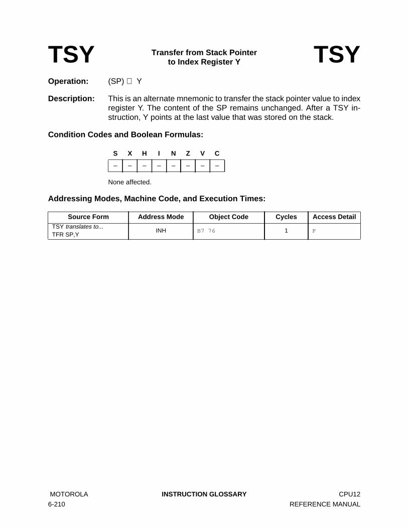
Operation: (SP) ⇒ Y
Description: This is an alternate mnemonic to transfer the stack pointer value to indexregister Y. The content of the SP remains unchanged. After a TSY in-struction, Y points at the last value that was stored on the stack.
Condition Codes and Boolean Formulas:
None affected.
Addressing Modes, Machine Code, and Execution Times:
TSY Transfer from Stack Pointerto Index Register Y TSY
S X H I N Z V C
– – – – – – – –
Source Form Address Mode Object Code Cycles Access DetailTSY translates to...TFR SP,Y
INH B7 76 1 P
MOTOROLA INSTRUCTION GLOSSARY CPU12
6-210 REFERENCE MANUAL

Operation: (X) ⇒ SP
Description: This is an alternate mnemonic to transfer index register X value to thestack pointer. The content of X is unchanged.
Condition Codes and Boolean Formulas:
None affected.
Addressing Modes, Machine Code, and Execution Times:
TXS Transfer from Index Register Xto Stack Pointer TXS
S X H I N Z V C
– – – – – – – –
Source Form Address Mode Object Code Cycles Access DetailTXS translates to...TFR X,SP
INH B7 57 1 P
CPU12 INSTRUCTION GLOSSARY MOTOROLA
REFERENCE MANUAL 6-211

Operation: (Y) ⇒ SP
Description: This is an alternate mnemonic to transfer index register Y value to thestack pointer. The content of Y is unchanged.
Condition Codes and Boolean Formulas:
None affected.
Addressing Modes, Machine Code, and Execution Times:
TYS Transfer from Index Register Yto Stack Pointer TYS
S X H I N Z V C
– – – – – – – –
Source Form Address Mode Object Code Cycles Access DetailTYS translates to...TFR Y,SP
INH B7 67 1 P
MOTOROLA INSTRUCTION GLOSSARY CPU12
6-212 REFERENCE MANUAL

Operation: (SP) – $0002 ⇒ SP; RTNH : RTNL ⇒ (M(SP) : M(SP + 1))(SP) – $0002 ⇒ SP; YH : YL ⇒ (M(SP) : M(SP + 1))(SP) – $0002 ⇒ SP; XH : XL ⇒ (M(SP) : M(SP + 1))(SP) – $0002 ⇒ SP; B : A⇒ (M(SP) : M(SP + 1))(SP) – $0001 ⇒ SP; CCR ⇒ (M(SP))Stop CPU Clocks
Description: Puts the CPU into a wait state. Uses the address of the instruction fol-lowing WAI as a return address. Stacks the return address, index regis-ters Y and X, accumulators B and A, and the CCR, decrementing the SPbefore each item is stacked.
The CPU then enters a wait state for an integer number of bus clock cy-cles. During the wait state, CPU clocks are stopped, but other MCUclocks can continue to run. The CPU leaves the wait state when it sens-es an interrupt that has not been masked.
Upon leaving the wait state, the CPU sets the appropriate interrupt maskbit(s), fetches the vector corresponding to the interrupt sensed, and in-struction execution continues at the location the vector points to.
Condition Codes and Boolean Formulas:
Although the WAI instruction itself does not alter the condition codes,the interrupt that causes the CPU to resume processing also causesthe I mask bit (and the X mask bit, if the interrupt was XIRQ) to be setas the interrupt vector is fetched.
Addressing Modes, Machine Code, and Execution Times:
WAI Wait for Interrupt WAI
S X H I N Z V C
– – – – – – – –
Source Form Address Mode Object Code Cycles Access DetailWAI (before interrupt) INH 3E 8 OSSSfSsf
(when interrupt comes) 5 VfPPP
CPU12 INSTRUCTION GLOSSARY MOTOROLA
REFERENCE MANUAL 6-213

Operation: Do until B = 0, leave SOP in Y : D, SOW in X
Partial Product = (M pointed to by X) × (M pointed to by Y)Sum-of-Products (24-bit SOP) = Previous SOP + Partial ProductSum-of-Weights (16-bit SOW) = Previous SOW + (M pointed to by Y)(X) + $0001 ⇒ X; (Y) + $0001 ⇒ Y(B) – $01 ⇒ B
Description: Performs weighted average calculations on values stored in memory.Uses indexed (X) addressing mode to reference one source operand list,and indexed (Y) addressing mode to reference a second source operandlist. Accumulator B is used as a counter to control the number of ele-ments to be included in the weighted average.
For each pair of data points, a 24-bit sum of products (SOP) and a 16-bit sum of weights (SOW) is accumulated in temporary registers. WhenB reaches zero (no more data pairs), the SOP is placed in Y : D. TheSOW is placed in X. To arrive at the final weighted average, divide thecontent of Y : D by X by executing an EDIV after the WAV.
This instruction can be interrupted. If an interrupt occurs during WAV ex-ecution, the intermediate results (six bytes) are stacked in the orderSOW[15:0], SOP[15:0], $00:SOP[23:16] before the interrupt is processed.The wavr pseudo-instruction is used to resume execution after an inter-rupt. The mechanism is re-entrant. New WAV instructions can be startedand interrupted while a previous WAV instruction is interrupted.
This instruction is often used in fuzzy logic rule evaluation. Refer to SEC-TION 9 FUZZY LOGIC SUPPORT for more information.
Condition Codes and Boolean Formulas:
Addressing Modes, Machine Code, and Execution Times:
WAV Weighted Average WAV
S X H I N Z V C
– – ? – ? 1 ? ?
Z: 1; Set.
H, N, V and C may be altered by this instruction.
Source Form Address Mode Object Code Cycles Access DetailWAV(add if interrupted)
Special 18 3C See note1
Notes:1. The 8-cycle sequence in parentheses represents the loop for one iteration of SOP and SOW accumulation.
Off(frrfffff)O
SSSUUUrr
MOTOROLA INSTRUCTION GLOSSARY CPU12
6-214 REFERENCE MANUAL

Operation: (D) ⇔ (X)
Description: Exchanges the content of double accumulator D and the content of indexregister X. For compatibility with the M68HC11, the XGDX instruction istranslated into an EXG D,X instruction by the assembler.
Condition Codes and Boolean Formulas:
None affected.
Addressing Modes, Machine Code, and Execution Times:
XGDX Exchange Double Accumulatorand Index Register X XGDX
S X H I N Z V C
– – – – – – – –
Source Form Address Mode Object Code Cycles Access DetailXGDX translates to...EXG D,X
INH B7 C5 1 P
CPU12 INSTRUCTION GLOSSARY MOTOROLA
REFERENCE MANUAL 6-215

Operation: (D) ⇔ (Y)
Description: Exchanges the content of double accumulator D and the content of indexregister Y. For compatibility with the M68HC11, the XGDY instruction istranslated into an EXG D,Y instruction by the assembler.
Condition Codes and Boolean Formulas:
None affected.
Addressing Modes, Machine Code, and Execution Times:
XGDY Exchange Double Accumulatorand Index Register Y XGDY
S X H I N Z V C
– – – – – – – –
Source Form Address Mode Object Code Cycles Access DetailXGDY translates to...EXG D,Y
INH B7 C6 1 P
MOTOROLA INSTRUCTION GLOSSARY CPU12
6-216 REFERENCE MANUAL

SECTION 7EXCEPTION PROCESSING
Exceptions are events that require processing outside the normal flow of instructionexecution. This section describes exceptions and the way each is handled.
7.1 Types of Exceptions
CPU12 exceptions include resets, an unimplemented opcode trap, a software interruptinstruction, X-bit interrupts, and I-bit interrupts. Each exception has an associated 16-bit vector, which points to the memory location where the routine that handles the ex-ception is located. As shown in Table 7-1 , vectors are stored in the upper 128 bytesof the standard 64-Kbyte address map.
The six highest vector addresses are used for resets and unmaskable interrupt sourc-es. The remaining vectors are used for maskable interrupts. All vectors must be pro-grammed to point to the address of the appropriate service routine.
The CPU12 can handle up to 64 exception vectors, but the number actually used var-ies from device to device, and some vectors are reserved for Motorola use. Refer todevice documentation for more information.
Exceptions can be classified by the effect of the X and I interrupt mask bits on recog-nition of a pending request.
Resets, the unimplemented opcode trap, and the SWI instruction are not affectedby the X and I mask bits.
Interrupt service requests from the XIRQ pin are inhibited when X = 1, but are notaffected by the I bit.
All other interrupts are inhibited when I = 1.
Table 7-1 CPU12 Exception Vector Map
Vector Address Source
$FFFE–$FFFF System Reset
$FFFC–$FFFD Clock Monitor Reset
$FFFA–$FFFB COP Reset
$FFF8–$FFF9 Unimplemented Opcode Trap
$FFF6–$FFF7 Software Interrupt Instruction (SWI)
$FFF4–$FFF5 XIRQ Signal
$FFF2–$FFF3 IRQ Signal
$FFC0–$FFF1 Device-Specific Interrupt Sources
CPU12 EXCEPTION PROCESSING MOTOROLA
REFERENCE MANUAL 7-1

7.2 Exception Priority
A hardware priority hierarchy determines which reset or interrupt is serviced first whensimultaneous requests are made. Six sources are not maskable. The remaining sourc-es are maskable, and the device integration module typically can change the relativepriorities of maskable interrupts. Refer to 7.4 Interrupts for more detail concerning in-terrupt priority and servicing.
The priorities of the unmaskable sources are:
1. RESET pin2. Clock monitor reset3. COP watchdog reset4. XIRQ signal5. Unimplemented opcode trap6. Software interrupt instruction (SWI)
An external reset has the highest exception-processing priority, followed by clockmonitor reset, and then the on-chip watchdog reset.
The XIRQ interrupt is pseudo-non-maskable. After reset, the X bit in the CCR is set,which inhibits all interrupt service requests from the XIRQ pin until the X bit is cleared.The X bit can be cleared by a program instruction, but program instructions cannot re-set X from zero to one. Once the X bit is cleared, interrupt service requests made viathe XIRQ pin become non-maskable.
The unimplemented page 2 opcode trap (TRAP) and the software interrupt instruction(SWI) are special cases. In one sense, these two exceptions have very low priority,because any enabled interrupt source that is pending prior to the time exception pro-cessing begins will take precedence. However, once the CPU begins processing aTRAP or SWI, neither can be interrupted. Also, since these are mutually exclusive in-structions, they have no relative priority.
All remaining interrupts are subject to masking via the I bit in the CCR. Most M68HC12MCUs have an external IRQ pin, which is assigned the highest I-bit interrupt priority,and an internal periodic real-time interrupt generator, which has the next highest pri-ority. The other maskable sources have default priorities that follow the address orderof the interrupt vectors — the higher the address, the higher the priority of the interrupt.Other maskable interrupts are associated with on-chip peripherals such as timers orserial ports. Typically, logic in the device integration module can give one I-maskedsource priority over other I-masked sources. Refer to the documentation for the spe-cific M68HC12 derivative for more information.
7.3 Resets
M68HC12 devices perform resets with a combination of hardware and software. Inte-gration module circuitry determines the type of reset that has occurred, performs basicsystem configuration, then passes control to the CPU12. The CPU fetches a vectordetermined by the type of reset that has occurred, jumps to the address pointed to bythe vector, and begins to execute code at that address.
MOTOROLA EXCEPTION PROCESSING CPU12
7-2 REFERENCE MANUAL

There are four possible sources of reset. Power-on reset (POR) and external resetshare the same reset vector. The computer operating properly (COP) reset and theclock monitor reset each have a vector.
7.3.1 Power-On Reset
The M68HC12 device integration module incorporates circuitry to detect a positivetransition in the VDD supply and initialize the device during cold starts, generally byasserting the reset signal internally. The signal is typically released after a delay thatallows the device clock generator to stabilize.
7.3.2 External Reset
The MCU distinguishes between internal and external resets by sensing how quicklythe signal on the RESET pin rises to logic level one after it has been asserted. Whenthe MCU senses any of the four reset conditions, internal circuitry drives the RESETsignal low for 16 clock cycles, then releases. Eight clock cycles later, the MCU sam-ples the state of the signal applied to the RESET pin. If the signal is still low, an exter-nal reset has occurred. If the signal is high, reset has been initiated internally by eitherthe COP system or the clock monitor.
7.3.3 COP Reset
The MCU includes a computer operating properly (COP) system to help protectagainst software failures. When the COP is enabled, software must write a particularcode sequence to a specific address in order to keep a watchdog timer from timing out.If software fails to execute the sequence properly, a reset occurs.
7.3.4 Clock Monitor Reset
The clock monitor circuit uses an internal RC circuit to determine whether clock fre-quency is above a predetermined limit. If clock frequency falls below the limit when theclock monitor is enabled, a reset occurs.
7.4 Interrupts
Each M68HC12 device can recognize a number of interrupt sources. Each source hasa vector in the vector table. The XIRQ signal, the unimplemented opcode trap, and theSWI instruction are non-maskable, and have a fixed priority. The remaining interruptsources can be masked by the I bit. In most M68HC12 devices, the external interruptrequest pin is assigned the highest maskable interrupt priority, and the internal period-ic real-time interrupt generator has the next highest priority. Other maskable interruptsare associated with on-chip peripherals such as timers or serial ports. These maskablesources have default priorities that follow the address order of the interrupt vectors.The higher the vector address, the higher the priority of the interrupt. Typically, a de-vice integration module incorporates logic that can give one maskable source priorityover other maskable sources.
CPU12 EXCEPTION PROCESSING MOTOROLA
REFERENCE MANUAL 7-3

7.4.1 Non-Maskable Interrupt Request ( XIRQ)
The XIRQ input is an updated version of the NMI input of earlier MCUs. The XIRQfunction is disabled during system reset and upon entering the interrupt service routinefor an XIRQ interrupt.
During reset, both the I bit and the X bit in the CCR are set. This disables maskableinterrupts and interrupt service requests made by asserting the XIRQ signal. After min-imum system initialization, software can clear the X bit using an instruction such asANDCC #$BF. Software cannot reset the X bit from zero to one once it has beencleared, and interrupt requests made via the XIRQ pin become non-maskable. Whena non-maskable interrupt is recognized, both the X and I bits are set after context issaved. The X bit is not affected by maskable interrupts. Execution of an RTI at the endof the interrupt service routine normally restores the X and I bits to the pre-interruptrequest state.
7.4.2 Maskable Interrupts
Maskable interrupt sources include on-chip peripheral systems and external interruptservice requests. Interrupts from these sources are recognized when the global inter-rupt mask bit (I) in the CCR is cleared. The default state of the I bit out of reset is one,but it can be written at any time.
The integration module manages maskable interrupt priorities. Typically, an on-chipinterrupt source is subject to masking by associated bits in control registers in additionto global masking by the I bit in the CCR. Sources generally must be enabled by writingone or more bits in associated control registers. There may be other interrupt-relatedcontrol bits and flags, and there may be specific register read-write sequences asso-ciated with interrupt service. Refer to individual on-chip peripheral descriptions for de-tails.
7.4.3 Interrupt Recognition
Once enabled, an interrupt request can be recognized at any time after the I mask bitis cleared. When an interrupt service request is recognized, the CPU responds at thecompletion of the instruction being executed. Interrupt latency varies according to thenumber of cycles required to complete the current instruction. Because the REV,REVW and WAV instructions can take many cycles to complete, they are designed sothat they can be interrupted. Instruction execution resumes when interrupt executionis complete. When the CPU begins to service an interrupt, the instruction queue is re-filled, a return address is calculated, and then the return address and the contents ofthe CPU registers are stacked as shown in Table 7-2 .
After the CCR is stacked, the I bit (and the X bit, if an XIRQ interrupt service requestcaused the interrupt) is set to prevent other interrupts from disrupting the interrupt ser-vice routine. Execution continues at the address pointed to by the vector for the high-est-priority interrupt that was pending at the beginning of the interrupt sequence. Atthe end of the interrupt service routine, an RTI instruction restores context from thestacked registers, and normal program execution resumes.
MOTOROLA EXCEPTION PROCESSING CPU12
7-4 REFERENCE MANUAL

7.4.4 External Interrupts
External interrupt service requests are made by asserting an active-low signal con-nected to the IRQ pin. Typically, control bits in the device integration module affecthow the signal is detected and recognized.
The I bit serves as the IRQ interrupt enable flag. When an IRQ interrupt is recognized,the I bit is set to inhibit interrupts during the interrupt service routine. Before othermaskable interrupt requests can be recognized, the I bit must be cleared. This is gen-erally done by an RTI instruction at the end of the service routine.
7.4.5 Return from Interrupt Instruction (RTI)
RTI is used to terminate interrupt service routines. RTI is an 8-cycle instruction whenno other interrupt is pending, and a 10-cycle instruction when another interrupt ispending. In either case, the first five cycles are used to restore (pull) the CCR, B:A, X,Y, and the return address from the stack. If no other interrupt is pending at this point,three program words are fetched to refill the instruction queue from the area of the re-turn address and processing proceeds from there.
If another interrupt is pending after registers are restored, a new vector is fetched, andthe stack pointer is adjusted to point at the CCR value that was just recovered (SP =SP – 9). This makes it appear that the registers have been stacked again. After the SPis adjusted, three program words are fetched to refill the instruction queue, starting atthe address the vector points to. Processing then continues with execution of the in-struction that is now at the head of the queue.
7.5 Unimplemented Opcode Trap
The CPU12 has opcodes in all 256 positions in the page 1 opcode map, but only 54of the 256 positions on page 2 of the opcode map are used. If the CPU attempts toexecute one of the 202 unused opcodes on page 2, an unimplemented opcode trapoccurs. The 202 unimplemented opcodes are essentially interrupts that share a com-mon interrupt vector, $FFF8:$FFF9.
The CPU12 uses the next address after an unimplemented page 2 opcode as a returnaddress. This differs from the M68HC11 illegal opcode interrupt, which uses the ad-dress of an illegal opcode as the return address. In the CPU12, the stacked return ad-dress can be used to calculate the address of the unimplemented opcode for software-controlled traps.
Table 7-2 Stacking Order on Entry to Interrupts
Memory Location CPU Registers
SP RTNH : RTNL
SP +2 YH : YL
SP +4 XH : XL
SP +6 B : A
SP +8 CCR
CPU12 EXCEPTION PROCESSING MOTOROLA
REFERENCE MANUAL 7-5
7.6 Software Interrupt Instruction
Execution of the SWI instruction causes an interrupt without an interrupt service re-quest. SWI is not inhibited by the global mask bits in the CCR, and execution of SWIsets the I mask bit. Once an SWI interrupt begins, maskable interrupts are inhibiteduntil the I bit in the CCR is cleared. This typically occurs when an RTI instruction at theend of the SWI service routine restores context.
7.7 Exception Processing Flow
The first cycle in the exception processing flow for all CPU12 exceptions is the same,regardless of the source of the exception. Between the first and second cycles of ex-ecution, the CPU chooses one of three alternative paths. The first path is for resets,the second path is for pending X or I interrupts, and the third path is used for softwareinterrupts (SWI) and trapping unimplemented opcodes. The last two paths are virtuallyidentical, differing only in the details of calculating the return address. Refer to Figure7-2 for the following discussion.
7.7.1 Vector Fetch
The first cycle of all exception processing, regardless of the cause, is a vector fetch.The vector points to the address where exception processing will continue. Exceptionvectors are stored in a table located at the top of the memory map ($FFC0–$FFFF).The CPU cannot use the fetched vector until the third cycle of the exception process-ing sequence.
During the vector fetch cycle, the CPU issues a signal that tells the integration moduleto drive the vector address of the highest priority, pending exception onto the systemaddress bus (the CPU does not provide this address).
After the vector fetch, the CPU selects one of the three alternate execution paths, de-pending upon the cause of the exception.
7.7.2 Reset Exception Processing
If reset caused the exception, processing continues to cycle 2.0. This cycle sets the Xand I bits in the CCR. The stack pointer is also decremented by two, but this is an ar-tifact of shared code used for interrupt processing; the SP is not intended to have anyspecific value after a reset. Cycles 3.0 through 5.0 are program word fetches that refillthe instruction queue. Fetches start at the address pointed to by the reset vector.When the fetches are completed, exception processing ends, and the CPU starts ex-ecuting the instruction at the head of the instruction queue.
MOTOROLA EXCEPTION PROCESSING CPU12
7-6 REFERENCE MANUAL

Figure 7-2 Exception Processing Flow Diagram
1.0 - V Fetch vector
2.0 - f No bus access
Set X and I; SP–2 ⇒SP
START
END
No
YesReset?
Interrupt?
2.1 - S Push return address
Address of inst that would have
2.2 - S Push return address
Address of inst after SWI orexecuted if no interrupt unimplemented opcode
3.0 - P Fetch program word
Start to fill instruction queue
4.0 - P Fetch program word
Continue to fill instruction queue
5.0 - P Fetch program word
Finish filling instruction queue
3.2 - P Fetch program word
Start to fill instruction queue
4.2 - S Push Y
6.2 - P Fetch program word
Continue to fill instruction queue
9.2 - P Fetch program word
Finish filling instruction queue
5.2 - S Push X
Transfer B:A to 16-bit temp reg
7.2 - S Push B:A
8.2 - s Push CCR (byte)Set I bit
END
3.1 - P Fetch program word
Start to fill instruction queue
4.1 - S Push Y
6.1 - P Fetch program word
Continue to fill instruction queue
9.1 - P Fetch program word
Finish filling instruction queue
5.1 - S Push X
Transfer B:A to 16-bit temp reg
7.1 - S Push B:A
8.1 - s Push CCR (byte)
Set I bitIf XIRQ, set X bit
END
No
Yes
CPU12EXPFLOW
Opcode trap?Yes
T.1 - f Internal calculations
No
CPU12 EXCEPTION PROCESSING MOTOROLA
REFERENCE MANUAL 7-7

7.7.3 Interrupt and Unimplemented Opcode Trap Exception Processing
If an exception was not caused by a reset, a return address is calculated.
Cycles 2.1and 2.2 are both S cycles (a 16-bit word), but the cycles are not identicalbecause the CPU12 performs different return address calculations for each type of ex-ception.
When an X- or I-related interrupt causes the exception, the return address pointsto the next instruction that would have been executed had processing not been in-terrupted.
When an exception is caused by an SWI opcode or by an unimplemented opcode(see 7.5 Unimplemented Opcode Trap ), the return address points to the next ad-dress after the opcode.
Once calculated, the return address is pushed onto the stack.
Cycles 3.1 through 9.1 are identical to cycles 3.2 through 9.2 for the rest of the se-quence, except for X mask bit manipulation performed in cycle 8.1.
Cycle 3.1/3.2 is the first of three program word fetches that refill the instruction queue.
Cycle 4.1/4.2 pushes Y onto the stack.
Cycle 5.1/5.2 pushes X onto the stack.
Cycle 6.1/6.2 is the second of three program word fetches that refill the instructionqueue. During this cycle, the contents of the A and B accumulators are concatenatedinto a 16-bit word in the order B:A. This makes register order in the stack frame thesame as that of the M68HC11, M6801, and the M6800.
Cycle 7.1/7.2 pushes the 16-bit word containing B:A onto the stack.
Cycle 8.1/8.2 pushes the 8-bit CCR onto the stack, then updates the mask bits.
When an XIRQ interrupt causes an exception, both X and I are set, which inhibitsfurther interrupts during exception processing.
When any other interrupt causes an exception, the I bit is set, but the X bit is notchanged.
Cycle 9.1/9.2 is the third of three program word fetches that refill the instruction queue.It is the last cycle of exception processing. After this cycle the CPU starts executingthe first cycle of the instruction at the head of the instruction queue.
MOTOROLA EXCEPTION PROCESSING CPU12
7-8 REFERENCE MANUAL
SECTION 8DEVELOPMENT AND DEBUG SUPPORT
This section is an explanation of CPU-related aspects of the background debuggingsystem. Topics include the instruction queue status signals, instruction tagging, andthe single-wire background debug interface.
8.1 External Reconstruction of the Queue
The CPU12 uses an instruction queue to buffer program information and increase in-struction throughput. The queue consists of two 16-bit stages, plus a 16-bit holdinglatch. Program information is always fetched in aligned 16-bit words. At least threebytes of program information are available to the CPU when instruction execution be-gins. The holding latch is used when a word of program information arrives before thequeue can advance.
Because of the queue, program information is fetched a few cycles before it is usedby the CPU. Internally, the MCU only needs to buffer the fetched data. But, in order tomonitor cycle-by-cycle CPU activity, it is necessary to externally reconstruct what ishappening in the instruction queue.
Two external pins, IPIPE[1:0], provide time-multiplexed information about data move-ment in the queue and instruction execution. To complete the picture for system de-bugging, it is also necessary to include program information and associated addressesin the reconstructed queue.
The instruction queue and cycle-by-cycle activity can be reconstructed in real time orfrom trace history captured by a logic analyzer. However, neither scheme can be usedto stop the CPU12 at a specific instruction. By the time an operation is visible outsidethe MCU, the instruction has already begun execution. A separate instruction taggingmechanism is provided for this purpose. A tag follows the information in the queue asthe queue is advanced. During debugging, the CPU enters active background debugmode when a tagged instruction reaches the head of the queue, rather than executingthe tagged instruction. For more information about tagging, refer to 8.5 InstructionTagging .
8.2 Instruction Queue Status Signals
The IPIPE[1:0] signals carry time-multiplexed information about data movement andinstruction execution during normal CPU operation. The signals are available on twomultifunctional device pins. During reset, the pins are used as mode-select input sig-nals MODA and MODB. After reset, information on the pins does not become valid un-til an instruction reaches queue stage 2.
CPU12 DEVELOPMENT AND DEBUG SUPPORT MOTOROLA
REFERENCE MANUAL 8-1

To reconstruct the queue, the information carried by the status signals must be cap-tured externally. In general, data movement and execution start information are con-sidered to be distinct 2-bit values, with the low-order bit on IPIPE0 and the high-orderbit on IPIPE1. Data movement information is available on rising edges of the E clock;execution start information is available on falling edges of the E clock, as shown in Fig-ure 8-1 . Data movement information refers to data on the bus at the previous fallingedge of E. Execution information refers to the bus cycle from the current falling edgeto the next falling edge of E. Table 8-1 summarizes the information encoded on theIPIPE[1:0] pins.
Figure 8-1 Queue Status Signal Timing
Table 8-1 IPIPE[1:0] Decoding
Data Movement(capture at E rise)
Mnemonic Meaning
0:0 — No movement
0:1 LAT Latch data from bus
1:0 ALD Advance queue and load from bus
1:1 ALL Advance queue and load from latch
Execution Start(capture at E fall)
Mnemonic Meaning
0:0 — No start
0:1 INT Start interrupt sequence
1:0 SEV Start even instruction
1:1 SOD Start odd instruction
QUE STATUS TIM
ECLK
ADDR
DATA
IPIPE[1:0] EX1 DM0 EX2 DM1 EX3
EX1 REFERS TO THIS CYCLE
DM0 REFERS TO DATA CAPTUREDON THIS ECLK TRANSITION
MOTOROLA DEVELOPMENT AND DEBUG SUPPORT CPU12
8-2 REFERENCE MANUAL

8.2.1 Zero Encoding (0:0)
The 0:0 state at the rising edge of E indicates that there was no data movement in theinstruction queue during the previous cycle; the 0:0 state at the falling edge of E indi-cates continuation of an instruction or interrupt sequence.
8.2.2 LAT — Latch Data from Bus Encoding (0:1)
Fetched program information has arrived, but the queue is not ready to advance. Theinformation is latched into the buffer. Later, when the queue does advance, stage 1 isrefilled from the buffer, or from the data bus if the buffer is empty. In some instructionsequences, there can be several latch cycles before the queue advances. In thesecases, the buffer is filled on the first latch event and additional latch requests are ig-nored.
8.2.3 ALD — Advance and Load from Data Bus Encoding (1:0)
The two-stage instruction queue is advanced by one word and stage 1 is refilled witha word of program information from the data bus. The CPU requested the informationtwo bus cycles earlier but, due to access delays, the information was not available untilthe E cycle immediately prior to the ALD.
8.2.4 ALL — Advance and Load from Latch Encoding (1:1)
The two-stage instruction queue is advanced by one word and stage 1 is refilled witha word of program information from the buffer. The information was latched from thedata bus at the falling edge of a previous E cycle because the instruction queue wasnot ready to advance when it arrived.
8.2.5 INT — Interrupt Sequence Encoding (0:1)
The E cycle starting at this E fall is the first cycle of an interrupt sequence. Normallythis cycle is a read of the interrupt vector. However, in systems that have interrupt vec-tors in external memory and an 8-bit data bus, this cycle reads only the upper byte ofthe 16-bit interrupt vector.
8.2.6 SEV — Start Instruction on Even Address Encoding (1:0)
The E cycle starting at this E fall is the first cycle of the instruction in the even (highorder) half of the word at the head of the instruction queue. The queue treats the $18prebyte for instructions on page 2 of the opcode map as a special 1-byte, 1-cycle in-struction, except that interrupts are not recognized at the boundary between the pre-byte and the rest of the instruction.
8.2.7 SOD — Start Instruction on Odd Address Encoding (1:1)
The E cycle starting at this E fall is the first cycle of the instruction in the odd (low order)half of the word at the head of the instruction queue. The queue treats the $18 prebytefor instructions on page 2 of the opcode map as a special 1-byte, 1-cycle instruction,except that interrupts are not recognized at the boundary between the prebyte and therest of the instruction.
CPU12 DEVELOPMENT AND DEBUG SUPPORT MOTOROLA
REFERENCE MANUAL 8-3

8.3 Implementing Queue Reconstruction
The raw signals required for queue reconstruction are the address bus (ADDR), thedata bus (DATA), the read/write strobe (R/W), the system clock (E), and the queue sta-tus signals (IPIPE[1:0]). An E clock cycle begins after an E fall. Addresses, R/W state,and data movement status must be captured at the E rise in the middle of the cycle.Data and execution start status must be captured at the E fall at the end of the cycle.These captures can then be organized into records with one record per E clock cycle.
Implementation details depend upon the type of device and the mode of operation. Forinstance, the data bus can be eight bits or 16 bits wide, and non-multiplexed or multi-plexed. In all cases, the externally reconstructed queue must use 16-bit words. Demul-tiplexing and assembly of 8-bit data into 16-bit words is done before programinformation enters the real queue, so it must also be done for the external reconstruc-tion. An example:
Systems with an 8-bit data bus and a program stored in external memory requiretwo cycles for each program word fetch. MCU bus control logic freezes the CPUclocks long enough to do two 8-bit accesses rather than a single 16-bit access, sothe CPU sees only 16-bit words of program information. To recover the 16-bit pro-gram words externally, latch the data bus state at the falling edge of E whenADDR0 = 0, and gate the outputs of the latch onto DATA[15:8] when a LAT or ALDcycle occurs. Since the 8-bit data bus is connected to DATA[7:0], the 16-bit wordon the data lines corresponds to the ALD or LAT status indication at the E rise afterthe second 8-bit fetch, which is always to an odd address. IPIPE[1:0] status signalsindicate 0:0 at the beginning (E fall) and middle (E rise) of the first 8-bit fetch.
Some M68HC12 devices have address lines to support memory expansion beyondthe standard 64-Kbyte address space. When memory expansion is used, expandedaddresses must also be captured and maintained.
8.3.1 Queue Status Registers
Queue reconstruction requires the following registers, which can be implemented assoftware variables when previously captured trace data is used, or as hardware latch-es in real time.
8.3.1.1 in_add, in_dat Registers
These registers contain the address and data from the previous external bus cycle.Depending upon how records are read and processed from the raw capture informa-tion, it may be possible to simply read this information from the raw capture data filewhen needed.
8.3.1.2 fetch_add, fetch_dat Registers
These registers buffer address and data for information that was fetched before thequeue was ready to advance.
MOTOROLA DEVELOPMENT AND DEBUG SUPPORT CPU12
8-4 REFERENCE MANUAL

8.3.1.3 st1_add, st1_dat Registers
These registers contain address and data for the first stage of the reconstructed in-struction queue.
8.3.1.4 st2_add, st2_dat Registers
These registers contain address and data for the final stage of the reconstructed in-struction queue. When the IPIPE[1:0] signals indicate that an instruction is starting toexecute, the address and opcode can be found in these registers.
8.3.2 Reconstruction Algorithm
This section describes in detail how to use IPIPE[1:0] signals and status storage reg-isters to perform queue reconstruction. An “is_full” flag is used to indicate when thefetch_add and fetch_dat buffer registers contain information. The use of the flag is ex-plained more fully in subsequent paragraphs.
Typically, the first few cycles of raw capture data are not useful because it takes sev-eral cycles before an instruction propagates to the head of the queue. During thesefirst raw cycles, the only meaningful information available are data movement signals.Information on the external address and data buses during this setup time reflects theactions of instructions that were fetched before data collection started.
In the special case of a reset, there is a five cycle sequence (VfPPP) during which thereset vector is fetched and the instruction queue is filled, before execution of the firstinstruction begins. Due to the timing of the switchover of the IPIPE[1:0] pins from theiralternate function as mode select inputs, the status information on these two pins maybe erroneous during the first cycle or two after the release of reset. This is not a prob-lem because the status is correct in time for queue reconstruction logic to correctly rep-licate the queue.
Before starting to reconstruct the queue, clear the is_full flag to indicate that there isno meaningful information in the fetch_add and fetch_dat buffers. Further movementof information in the instruction queue is based on the decoded status on theIPIPE[1:0] signals at the rising edges of E.
8.3.2.1 LAT Decoding
On a latch cycle, check the is_full flag. If and only if is_full = 0, transfer the addressand data from the previous bus cycle (in_add and in_dat) into the fetch_add andfetch_dat registers respectively. Then, set the is_full flag. The usual reason for a latchrequest instead of an advance request is that the previous instruction ended with a sin-gle aligned byte of program information in the last stage of the instruction queue. Sincethe odd half of this word still holds the opcode for the next instruction, the queue can-not advance on this cycle. However, the cycle to fetch the next word of program infor-mation has already started and the data is on its way.
CPU12 DEVELOPMENT AND DEBUG SUPPORT MOTOROLA
REFERENCE MANUAL 8-5

8.3.2.2 ALD Decoding
On an advance-and-load-from-data-bus cycle, the information in the instruction queuemust advance by one stage. Whatever was in stage 2 of the queue is simply thrownaway. The previous contents of stage 1 are moved to stage 2, and the address anddata from the previous cycle (in_add and in_dat) are transferred into stage 1 of the in-struction queue. Finally, clear the is_full flag to indicate the buffer latch is ready for newdata. Usually, there would be no useful information in the fetch buffer when an ALDcycle was encountered, but in the case of a change-of-flow, any data that was thereneeds to be flushed out (by clearing the is_full flag).
8.3.2.3 ALL Decoding
On an advance-and-load-from-latch cycle, the information in the instruction queuemust advance by one stage. Whatever was in stage 2 of the queue is simply thrownaway. The previous contents of stage 1 are moved to stage 2, and the contents of thefetch buffer latch are transferred into stage 1 of the instruction queue. One or more cy-cles preceding the ALL cycle will have been a LAT cycle. After updating the instructionqueue, clear the is_full flag to indicate the fetch buffer is ready for new information.
8.4 Background Debug Mode
M68HC12 MCUs include a resident debugging system. This system is implementedwith on-chip hardware rather than external software, and provides a full set of debug-ging options. The debugging system is less intrusive than systems used on other mi-crocontrollers, because the control logic resides in the on-chip integration module,rather than in the CPU. Some activities, such as reading and writing memory locations,can be performed while the CPU is executing normal code with no effect on real-timesystem activity.
The integration module generally uses CPU dead cycles to execute debugging com-mands while the CPU is operating normally, but can steal cycles from the CPU whennecessary. Other commands are firmware based, and require that the CPU be in ac-tive background debug mode (BDM) for execution. While BDM is active, the CPU ex-ecutes a monitor program located in a small on-chip ROM.
Debugging control logic communicates with external devices serially, via the BKGDpin. This single-wire approach helps to minimize the number of pins needed for devel-opment support.
Background debug does not operate in STOP mode.
8.4.1 Enabling BDM
The debugger must be enabled before it can be activated. Enabling has two phases.First, the BDM ROM must be enabled by writing the ENBDM bit in the BDM status reg-ister, using a debugging command sent via the single wire interface. Once the ROMis enabled, it remains available until the next system reset, or until ENBDM is clearedby another debugging command. Second, BDM must be activated to map the ROMand BDM control registers to addresses $FF00 to $FFFF and put the MCU in back-ground mode.
MOTOROLA DEVELOPMENT AND DEBUG SUPPORT CPU12
8-6 REFERENCE MANUAL

After the firmware is enabled, BDM can be activated by the hardware BACKGROUNDcommand, by breakpoints tagged via the LIM breakpoint logic or the BDM taggingmechanism, and by the BGND instruction. An attempt to activate BDM before firmwarehas been enabled causes the MCU to resume normal instruction execution after abrief delay.
BDM becomes active at the next instruction boundary following execution of the BDMBACKGROUND command. Breakpoints can be configured to activate BDM before atagged instruction is executed.
While BDM is active, BDM control registers are mapped to addresses $FF00 to $FF06.These registers are only accessible through BDM firmware or BDM hardware com-mands. 8.4.4 BDM Registers describes the registers.
Some M68HC12 on-chip peripherals have a BDM control bit, which determines wheth-er the peripheral function is available during BDM. If no bit is shown, the peripheral isactive in BDM.
8.4.2 BDM Serial Interface
The BDM serial interface uses a clocking scheme in which the external host generatesa falling edge on the BKGD pin to indicate the start of each bit time. This falling edgemust be sent for every bit, whether data is transmitted or received.
BKGD is an open drain pin that can be driven either by the MCU or by an external host.Data is transferred MSB first, at 16 E-clock cycles per bit. The interface times out if 512E-clock cycles occur between falling edges from the host. The hardware clears thecommand register when a time-out occurs.
The BKGD pin is used to send and receive data. The following diagrams show timingfor each of these cases. Interface timing is synchronous to MCU clocks, but the exter-nal host is asynchronous to the target MCU. The internal clock signal is shown for ref-erence in counting cycles.
Figure 8-2 shows an external host transmitting a data bit to the BKGD pin of a targetM68HC12 MCU. The host is asynchronous to the target, so there is a 0- to 1-cycle de-lay from the host-generated falling edge to the time when the target perceives the bit.Ten target E-cycles later, the target senses the bit level on the BKGD pin. The hostcan drive high during host-to-target transmission to speed up rising edges, becausethe target does not drive the pin during this time.
CPU12 DEVELOPMENT AND DEBUG SUPPORT MOTOROLA
REFERENCE MANUAL 8-7

Figure 8-2 BDM Host to Target Serial Bit Timing
Figure 8-3 shows an external host receiving a logic one from the target MCU. Sincethe host is asynchronous to the target, there is a 0- or 1-cycle delay from the host-gen-erated falling edge on BKGD until the target perceives the bit. The host holds the sig-nal low long enough for the target to recognize it (a minimum of two target E-clockcycles), but must release the low drive before the target begins to drive the active-highspeed-up pulse seven cycles after the start of the bit time. The host should sample thebit level about ten cycles after the start of bit time.
Figure 8-3 BDM Target to Host Serial Bit Timing (Logic 1)
10 CYCLES
ECLOCK(TARGET
MCU)
HOSTTRANSMIT 1
TARGET SENSES BIT
EARLIESTSTART OFNEXT BIT
SYNCHRONIZATIONUNCERTAINTY
PERCEIVED STARTOF BIT TIME
HOSTTRANSMIT 0
CPU12 BDM HT TIM
10 CYCLES
ECLOCK(TARGET
MCU)
EARLIESTSTART OFNEXT BIT
BKGD PIN
PERCEIVEDSTART OF BIT TIME
10 CYCLES
HOST SAMPLESBKGD PIN
HOSTDRIVE TOBKGD PIN
TARGET MCUSPEEDUP
PULSE
R-C RISE
HIGH-IMPEDANCE
HIGH-IMPEDANCE
HIGH-IMPEDANCE
CPU12 BDM TH TIM 1
MOTOROLA DEVELOPMENT AND DEBUG SUPPORT CPU12
8-8 REFERENCE MANUAL

Figure 8-4 shows the host receiving a logic zero from the target. Since the host isasynchronous to the target, there is a 0- or 1-cycle delay from the host-generated fall-ing edge on BKGD until the target perceives the bit. The host initiates the bit time, butthe target finishes it. To make certain the host receives a logic zero, the target drivesthe BKGD pin low for 13 E-clock cycles, then briefly drives the signal high to speed upthe rising edge. The host samples the bit level about ten cycles after starting the bittime.
Figure 8-4 BDM Target to Host Serial Bit Timing (Logic 0)
8.4.3 BDM Commands
All BDM opcodes are eight bits long, and can be followed by an address or data, asindicated by the instruction.
Commands implemented in BDM control hardware are listed in Table 8-2 . These com-mands, except for BACKGROUND, do not require the CPU to be in BDM mode for ex-ecution. The control logic uses CPU dead cycles to execute these instructions. If adead cycle cannot be found within 128 cycles, the control logic steals cycles from theCPU.
10 CYCLES
ECLOCK(TARGET
MCU)
EARLIESTSTART OFNEXT BIT
BKGD PIN
PERCEIVEDSTART OF BIT TIME
10 CYCLES
HOST SAMPLESBKGD PIN
HOSTDRIVE TOBKGD PIN
TARGET MCUDRIVE AND
SPEEDUP PULSE
HIGH-IMPEDANCE
SPEEDUP PULSE
CPU12 BDM TH0TIM
CPU12 DEVELOPMENT AND DEBUG SUPPORT MOTOROLA
REFERENCE MANUAL 8-9

The CPU must be in background mode to execute commands that are implementedin the BDM ROM. The CPU executes code from the ROM to perform the requestedoperation. These commands are shown in Table 8-3 .
The host controller must wait 150 cycles for a non-intrusive BDM command to executebefore another command can be sent. This delay includes 128 cycles for the maxi-mum delay for a dead cycle.
BDM logic retains control of the internal buses until a read or write is completed. If anoperation can be completed in a single cycle, it does not intrude on normal CPU oper-ation. However, if an operation requires multiple cycles, CPU clocks are frozen untilthe operation is complete.
Table 8-2 BDM Commands Implemented in Hardware
Command Opcode (Hex) Data Description
BACKGROUND 90 None Enter background mode (if firmware enabled).
READ_BD_BYTE E4 16-bit address16-bit data out
Read from memory with BDM in map (may steal cyclesif external access) data for odd address on low byte,data for even address on high byte.
STATUS1
NOTES:1. STATUS command is a specific case of the READ_BD_BYTE command.
E4 FF01, 0000 0000 (out)
READ_BD_BYTE $FF01. Running user code (BGNDinstruction is not allowed).
FF01,1000 0000 (out)
READ_BD_BYTE $FF01. BGND instruction is allowed.
FF01, 1100 0000 (out)
READ_BD_BYTE $FF01. Background mode active(waiting for single wire serial command).
READ_BD_WORD EC 16-bit address 16-bit data out
Read from memory with BDM in map (may steal cyclesif external access) must be aligned access.
READ_BYTE E0 16-bit address16-bit data out
Read from memory with BDM out of map (may steal cy-cles if external access) data for odd address on lowbyte, data for even address on high byte.
READ_WORD E8 16-bit address16-bit data out
Read from memory with BDM out of map (may steal cy-cles if external access) must be aligned access.
WRITE_BD_BYTE C4 16-bit address 16-bit data in
Write to memory with BDM in map (may steal cycles ifexternal access) data for odd address on low byte, datafor even address on high byte.
ENABLE_FIRMWARE2
2. ENABLE_FIRMWARE is a specific case of the WRITE_BD_BYTE command.
C4 FF01,1xxx xxxx(in)
Write byte $FF01, set the ENBDM bit. This allows exe-cution of commands which are implemented in firm-ware. Typically, read STATUS, OR in the MSB, writethe result back to STATUS.
WRITE_BD_WORD CC 16-bit address 16-bit data in
Write to memory with BDM in map (may steal cycles ifexternal access) must be aligned access.
WRITE_BYTE C0 16-bit address 16-bit data in
Write to memory with BDM out of map (may steal cyclesif external access) data for odd address on low byte,data for even address on high byte.
WRITE_WORD C8 16-bit address 16-bit data in
Write to memory with BDM out of map (may steal cyclesif external access) must be aligned access.
MOTOROLA DEVELOPMENT AND DEBUG SUPPORT CPU12
8-10 REFERENCE MANUAL

8.4.4 BDM Registers
Seven BDM registers are mapped into the standard 64-Kbyte address space whenBDM is active. Mapping is shown in Table 8-4 .
The content of the instruction register is determined by the type of background instruc-tion being executed. The status register indicates BDM operating conditions. The shiftregister contains data being received or transmitted via the serial interface. The ad-dress register is temporary storage for BDM commands. The CCR register preservesthe content of the CPU12 CCR while BDM is active.
The only register of interest to users is the status register. The other BDM registers areused only by the BDM firmware to execute commands. The registers can be accessedby means of the hardware READ_BD and WRITE_BD commands, but must not bewritten during BDM operation.
Table 8-3 BDM Firmware Commands
Command Opcode (Hex) Data Description
GO 08 none Resume normal processing
TRACE1 10 none Execute one user instruction then return to BDM
TAGGO 18 none Enable tagging then resume normal processing
WRITE_NEXT 42 16-bit data in X = X + 2; Write next word @ 0,X
WRITE_PC 43 16-bit data in Write program counter
WRITE_D 44 16-bit data in Write D accumulator
WRITE_X 45 16-bit data in Write X index register
WRITE_Y 46 16-bit data in Write Y index register
WRITE_SP 47 16-bit data in Write stack pointer
READ_NEXT 62 16-bit data out X = X + 2; Read next word @ 0,X
READ_PC 63 16-bit data out Read program counter
READ_D 64 16-bit data out Read D accumulator
READ_X 65 16-bit data out Read X index register
READ_Y 66 16-bit data out Read Y index register
READ_SP 67 16-bit data out Read stack pointer
Table 8-4 BDM Register Mapping
Address Register
$FF00 BDM instruction register
$FF01 BDM status register
$FF02–$FF03 BDM shift register
$FF04–$FF05 BDM address register
$FF06 BDM CCR register
CPU12 DEVELOPMENT AND DEBUG SUPPORT MOTOROLA
REFERENCE MANUAL 8-11

8.4.4.1 BDM Status Register
ENBDM — Enable BDM ROMShows whether the BDM ROM is enabled. Cleared by reset.
0 = BDM ROM not enabled1 = BDM ROM enabled, but not in memory map unless BDM is active
BDMACT — BDM Active FlagShows whether the BDM ROM is in the memory map. Cleared by reset.
0 = ROM not in map1 = ROM in map (MCU is in active BDM)
ENTAG — Instruction Tagging EnableShows whether instruction tagging is enabled. Set by the TAGGO instruction andcleared when BDM is entered. Cleared by reset.
NOTE
Execute a TAGGO command to enable instruction tagging. Do notwrite ENTAG directly.
0 = Tagging not enabled, or BDM active1 = Tagging active
SDV — Shifter Data ValidShows that valid data is in the serial interface shift register.
NOTE
SDV is used by firmware-based instructions. Do not attempt to writeSDV directly.
0 = No valid data1 = Valid Data
TRACE — Trace FlagShows when tracing is enabled.
NOTE
Execute a TRACE1 command to enable instruction tagging. Do notattempt to write TRACE directly.
0 = Tracing not enabled1 = Tracing active
STATUS — BDM Status Register $FF01
BIT 7 6 5 4 3 2 1 BIT 0
ENBDM BDMACT ENTAG SDV TRACE 0 0 0
RESET: 0 0 0 0 0 0 0 0
SP.S. CHIP &PERIPH.:
1 0 0 0 0 0 0 0
MOTOROLA DEVELOPMENT AND DEBUG SUPPORT CPU12
8-12 REFERENCE MANUAL

8.5 Instruction Tagging
The instruction queue and cycle-by-cycle CPU activity can be reconstructed in realtime, or from trace history that was captured by a logic analyzer. However, the recon-structed queue cannot be used to stop the CPU at a specific instruction, because ex-ecution has already begun by the time an operation is visible outside the MCU. Aseparate instruction tagging mechanism is provided for this purpose.
Executing the BDM TAGGO command configures two MCU pins for tagging. TheTAGLO signal shares a pin with the LSTRB signal, and the TAGHI signal shares a pinwith the BKGD pin. Tagging information is latched on the falling edge of ECLK, asshown in Figure 8-5 .
Figure 8-5 Tag Input Timing
Table 8-5 shows the functions of the two tagging pins. The pins operate independent-ly; the state of one pin does not affect the function of the other. The presence of logiclevel zero on either pin at the fall of ECLK performs the indicated function. Tagging isallowed in all modes. Tagging is disabled when BDM becomes active.
Table 8-5 Tag Pin Function
TAGHI TAGLO Tag
1 1 No Tag
1 0 Low Byte
0 1 High Byte
0 0 Both Bytes
CPU12 TAG TIM
ECLK
LSTRB/TAGLO
BKGD/TAGHI
TAGS ARE APPLIED TO PROGRAM INFORMATIONCAPTURED ON THIS ECLK TRANSITION
LSTRBVALID
TAGLOVALID
TAGHIVALID
CPU12 DEVELOPMENT AND DEBUG SUPPORT MOTOROLA
REFERENCE MANUAL 8-13

In M68HC12 derivatives that have hardware breakpoint capability, the breakpoint con-trol logic and BDM control logic use the same internal signals for instruction tagging.The CPU12 does not differentiate between the two kinds of tags.
The tag follows program information as it advances through the queue. When a taggedinstruction reaches the head of the queue, the CPU enters active background debugmode rather than executing the instruction.
8.6 Breakpoints
Breakpoints halt instruction execution at particular places in a program. To assuretransparent operation, breakpoint control logic is implemented outside the CPU, andparticular models of MCU can have different breakpoint capabilities. Refer to the ap-propriate device manual for detailed information. Generally, breakpoint logic can beconfigured to halt execution before an instruction executes, or to halt execution on thenext instruction boundary following the breakpoint.
8.6.1 Breakpoint Type
There are three basic types of breakpoints:
1. Address-only breakpoints that cause the CPU to execute an SWI. These break-points can be set only on addresses. When the breakpoint logic encounters thebreakpoint tag, the CPU12 executes an SWI instruction.
2. Address-only breakpoints that cause the MCU to enter BDM. These break-points can be set only on addresses. When the breakpoint logic encounters thebreakpoint tag, BDM is activated.
3. Address/data breakpoints that cause the MCU to enter BDM. These break-points can be set on an address, or on an address and data. When the break-point logic encounters the breakpoint tag, BDM is activated.
8.6.2 Breakpoint Operation
Breakpoints use two mechanisms to halt execution:
1. The tag mechanism marks a particular program fetch with a high (even) or low(odd) byte indicator. The tagged byte moves through the instruction queue untila start cycle occurs, then the breakpoint is taken. Breakpoint logic can be con-figured to force BDM, or to initiate an SWI when the tag is encountered.
2. The force BDM mechanism causes the MCU to enter active BDM at the nextinstruction start cycle.
CPU12 instructions are used to implement both breakpoint mechanisms. When anSWI tag is encountered, the CPU performs the same sequence of operations as for anSWI. When BDM is forced, the CPU executes a BGND instruction. However, becausethese operations are not part of the normal flow of instruction execution, the controlprogram must keep track of the actual breakpoint address.
MOTOROLA DEVELOPMENT AND DEBUG SUPPORT CPU12
8-14 REFERENCE MANUAL

Both SWI and BGND store a return PC value (SWI on the stack and BGND in theCPU12 TMP2 register), but this value is automatically incremented to point to the nextinstruction after SWI or BGND. In order to resume execution where a breakpoint oc-curred, the control program must preserve the breakpoint address rather than use theincremented PC value.
The breakpoint logic generally uses match registers to determine when a break is tak-en. Registers can be used to match the high and low bytes of addresses for single anddual breakpoints, to match data for single breakpoints, or to do both functions. Use ofthe registers is generally determined by control bit settings.
CPU12 DEVELOPMENT AND DEBUG SUPPORT MOTOROLA
REFERENCE MANUAL 8-15

MOTOROLA DEVELOPMENT AND DEBUG SUPPORT CPU12
8-16 REFERENCE MANUAL

SECTION 9FUZZY LOGIC SUPPORT
The CPU12 has the first microcontroller instruction set to specifically address theneeds of fuzzy logic. This section describes the use of fuzzy logic in control systems,discusses the CPU12 fuzzy logic instructions, and provides examples of fuzzy logicprograms.
9.1 Introduction
The CPU12 includes four instructions that perform specific fuzzy logic tasks. In addi-tion, several other instructions are especially useful in fuzzy logic programs. The over-all C-friendliness of the instruction set also aids development of efficient fuzzy logicprograms.
This section explains the basic fuzzy logic algorithm for which the four fuzzy logic in-structions are intended. Each of the fuzzy logic instructions are then explained in de-tail. Finally, other custom fuzzy logic algorithms are discussed, with emphasis on useof other CPU12 instructions.
The four fuzzy logic instructions are MEM, which evaluates trapezoidal membershipfunctions; REV and REVW, which perform unweighted or weighted MIN-MAX ruleevaluation; and WAV, which performs weighted average defuzzification on singletonoutput membership functions.
Other instructions that are useful for custom fuzzy logic programs include MINA,EMIND, MAXM, EMAXM, TBL, ETBL, and EMACS. For higher resolution fuzzy pro-grams, the fast extended precision math instructions in the CPU12 are also beneficial.Flexible indexed addressing modes help simplify access to fuzzy logic data structuresstored as lists or tabular data structures in memory.
The actual logic additions required to implement fuzzy logic support in the CPU12 arequite small, so there is no appreciable increase in cost for the typical user. A fuzzy in-ference kernel for the CPU12 requires one-fifth as much code space, and executesfifteen times faster than a comparable kernel implemented on a typical midrange mi-crocontroller. By incorporating fuzzy logic support into a high-volume, general-pur-pose microcontroller product family, Motorola has made fuzzy logic available for ahuge base of applications.
9.2 Fuzzy Logic Basics
This is an overview of basic fuzzy logic concepts. It can serve as a general introductionto the subject, but that is not the main purpose. There are a number of fuzzy logic pro-gramming strategies. This discussion concentrates on the methods implemented inthe CPU12 fuzzy logic instructions. The primary goal is to provide a background for adetailed explanation of the CPU12 fuzzy logic instructions.
CPU12 FUZZY LOGIC SUPPORT MOTOROLA
REFERENCE MANUAL 9-1

In general, fuzzy logic provides for set definitions that have fuzzy boundaries ratherthan the crisp boundaries of Aristotelian logic. These sets can overlap so that, for aspecific input value, one or more sets associated with linguistic labels may be true toa degree at the same time. As the input varies from the range of one set into the rangeof an adjacent set, the first set becomes progressively less true while the second setbecomes progressively more true.
Fuzzy logic has membership functions which emulate human concepts like “tempera-ture is warm”; that is, conditions are perceived to have gradual boundaries. This con-cept seems to be a key element of the human ability to solve certain types of complexproblems that have eluded traditional control methods.
Fuzzy sets provide a means of using linguistic expressions like “temperature is warm”in rules which can then be evaluated with a high degree of numerical precision andrepeatability. This directly contradicts the common misperception that fuzzy logic pro-duces approximate results — a specific set of input conditions always produces thesame result, just as a conventional control system does.
A microcontroller-based fuzzy logic control system has two parts. The first part is afuzzy inference kernel which is executed periodically to determine system outputsbased on current system inputs. The second part of the system is a knowledge basewhich contains membership functions and rules. Figure 9-1 is a block diagram of thiskind of fuzzy logic system.
The knowledge base can be developed by an application expert without any microcon-troller programming experience. Membership functions are simply expressions of theexpert’s understanding of the linguistic terms that describe the system to be controlled.Rules are ordinary language statements that describe the actions a human expertwould take to solve the application problem.
Rules and membership functions can be reduced to relatively simple data structures(the knowledge base) stored in nonvolatile memory. A fuzzy inference kernel can bewritten by a programmer who does not know how the application system works. Theonly thing the programmer needs to do with knowledge base information is store it inthe memory locations used by the kernel.
One execution pass through the fuzzy inference kernel generates system output sig-nals in response to current input conditions. The kernel is executed as often as neededto maintain control. If the kernel is executed more often than needed, processor band-width and power are wasted; delaying too long between passes can cause the systemto get too far out of control. Choosing a periodic rate for a fuzzy control system is thesame as it would be for a conventional control system.
MOTOROLA FUZZY LOGIC SUPPORT CPU12
9-2 REFERENCE MANUAL

Figure 9-1 Block Diagram of a Fuzzy Logic System
9.2.1 Fuzzification (MEM)
During the fuzzification step, the current system input values are compared againststored input membership functions to determine the degree to which each label ofeach system input is true. This is accomplished by finding the y-value for the currentinput value on a trapezoidal membership function for each label of each system input.The MEM instruction in the CPU12 performs this calculation for one label of one sys-tem input. To perform the complete fuzzification task for a system, several MEM in-structions must be executed, usually in a program loop structure.
Figure 9-2 shows a system of three input membership functions, one for each label ofthe system input. The x-axis of all three membership functions represents the rangeof possible values of the system input. The vertical line through all three membershipfunctions represents a specific system input value. The y-axis represents degree oftruth and varies from completely false ($00 or 0%) to completely true ($FF or 100%).The y-value where the vertical line intersects each of the membership functions, is thedegree to which the current input value matches the associated label for this systeminput. For example, the expression “temperature is warm” is 25% true ($40). The value$40 is stored to a RAM location, and is called a fuzzy input (in this case, the fuzzy inputfor “temperature is warm”). There is a RAM location for each fuzzy input (for each labelof each system input).
INPUTMEMBERSHIPFUNCTIONS
RULE LIST
OUTPUTMEMBERSHIPFUNCTIONS
FUZZIFICATION
RULE EVALUATION
DEFUZZIFICATION
FUZZYINFERENCE
KERNEL
KNOWLEDGEBASE
SYSTEMINPUTS
SYSTEMOUTPUTS
FUZZY INPUTS(IN RAM)
FUZZY OUTPUTS(IN RAM)
…
…
FUZ LOG BD
CPU12 FUZZY LOGIC SUPPORT MOTOROLA
REFERENCE MANUAL 9-3

Figure 9-2 Fuzzification Using Membership Functions
When the fuzzification step begins, the current value of the system input is in an accu-mulator of the CPU12, one index register points to the first membership function defi-nition in the knowledge base, and a second index register points to the first fuzzy inputin RAM. As each fuzzy input is calculated by executing a MEM instruction, the resultis stored to the fuzzy input and both pointers are updated automatically to point to thelocations associated with the next fuzzy input. The MEM instruction takes care of ev-erything except counting the number of labels per system input and loading the currentvalue of any subsequent system inputs.
The end result of the fuzzification step is a table of fuzzy inputs representing currentsystem conditions.
$00
$80
$FF
0˚F 32˚F 64˚F 96˚F 128˚F
$40
$C0HOT
$00
$80
$FF
0˚F 32˚F 64˚F 96˚F 128˚F
$40
$C0WARM
$00
$80
$FF
0˚F 32˚F 64˚F 96˚F 128˚F
$40
$C0COLD
CURRENT
IS 64˚FTEMPERATURE
MEMBERSHIP FUNCTIONSFOR TEMPERATURE FUZZY INPUTS
TEMPERATURE IS HOT
TEMPERATURE IS WARM
TEMPERATURE IS COLD
$00
$40
$C0
FUZ MEM FNCT
MOTOROLA FUZZY LOGIC SUPPORT CPU12
9-4 REFERENCE MANUAL

9.2.2 Rule Evaluation (REV and REVW)
Rule evaluation is the central element of a fuzzy logic inference program. This stepprocesses a list of rules from the knowledge base using current fuzzy input values fromRAM to produce a list of fuzzy outputs in RAM. These fuzzy outputs can be thought ofas raw suggestions for what the system output should be in response to the currentinput conditions. Before the results can be applied, the fuzzy outputs must be furtherprocessed, or defuzzified, to produce a single output value that represents the com-bined effect of all of the fuzzy outputs.
The CPU12 offers two variations of rule evaluation instructions. The REV instructionprovides for unweighted rules (all rules are considered to be equally important). TheREVW instruction is similar but allows each rule to have a separate weighting factorwhich is stored in a separate parallel data structure in the knowledge base. In additionto the weights, the two rule evaluation instructions also differ in the way rules are en-coded into the knowledge base.
An understanding of the structure and syntax of rules is needed to understand how amicrocontroller performs the rule evaluation task. The following is an example of a typ-ical rule.
If temperature is warm and pressure is high then heat is (should be) off.
At first glance, it seems that encoding this rule in a compact form understandable tothe microcontroller would be difficult, but it is actually simple to reduce the rule to asmall list of memory pointers. The left portion of the rule is a statement of input condi-tions and the right portion of the rule is a statement of output actions.
The left portion of a rule is made up of one or more (in this case two) antecedents con-nected by a fuzzy and operator. Each antecedent expression consists of the name ofa system input, followed by is, followed by a label name. The label must be defined bya membership function in the knowledge base. Each antecedent expression corre-sponds to one of the fuzzy inputs in RAM. Since and is the only operator allowed toconnect antecedent expressions, there is no need to include these in the encodedrule. The antecedents can be encoded as a simple list of pointers to (or addresses of)the fuzzy inputs to which they refer.
The right portion of a rule is made up of one or more (in this case one) consequents.Each consequent expression consists of the name of a system output, followed by is,followed by a label name. Each consequent expression corresponds to a specificfuzzy output in RAM. Consequents for a rule can be encoded as a simple list of point-ers to (or addresses of) the fuzzy outputs to which they refer.
The complete rules are stored in the knowledge base as a list of pointers or addressesof fuzzy inputs and fuzzy outputs. In order for the rule evaluation logic to work, theremust be some means of knowing which pointers refer to fuzzy inputs, and which referto fuzzy outputs. There also must be a way to know when the last rule in the systemhas been reached.
CPU12 FUZZY LOGIC SUPPORT MOTOROLA
REFERENCE MANUAL 9-5

One method of organization is to have a fixed number of rules with a specific numberof antecedents and consequents. A second method, employed in Motorola FreewareM68HC11 kernels, is to mark the end of the rule list with a reserved value, and use abit in the pointers to distinguish antecedents from consequents. A third method of or-ganization, used in the CPU12, is to mark the end of the rule list with a reserved value,and separate antecedents and consequents with another reserved value. This permitsany number of rules, and allows each rule to have any number of antecedents andconsequents, subject to the limits imposed by availability of system memory.
Each rule is evaluated sequentially, but the rules as a group are treated as if they wereall evaluated simultaneously. Two mathematical operations take place during ruleevaluation. The fuzzy and operator corresponds to the mathematical minimum opera-tion and the fuzzy or operation corresponds to the mathematical maximum operation.The fuzzy and is used to connect antecedents within a rule. The fuzzy or is impliedbetween successive rules. Before evaluating any rules, all fuzzy outputs are set tozero (meaning not true at all). As each rule is evaluated, the smallest (minimum) an-tecedent is taken to be the overall truth of the rule. This rule truth value is applied toeach consequent of the rule (by storing this value to the corresponding fuzzy output)unless the fuzzy output is already larger (maximum). If two rules affect the same fuzzyoutput, the rule that is most true governs the value in the fuzzy output because therules are connected by an implied fuzzy or.
In the case of rule weighting, the truth value for a rule is determined as usual by findingthe smallest rule antecedent. Before applying this truth value to the consequents forthe rule, the value is multiplied by a fraction from zero (rule disabled) to one (rule fullyenabled). The resulting modified truth value is then applied to the fuzzy outputs.
The end result of the rule evaluation step is a table of suggested or “raw” fuzzy outputsin RAM. These values were obtained by plugging current conditions (fuzzy input val-ues) into the system rules in the knowledge base. The raw results cannot be supplieddirectly to the system outputs because they may be ambiguous. For instance, one rawoutput can indicate that the system output should be medium with a degree of truth of50% while, at the same time, another indicates that the system output should be lowwith a degree of truth of 25%. The defuzzification step resolves these ambiguities.
9.2.3 Defuzzification (WAV)
The final step in the fuzzy logic program combines the raw fuzzy outputs into a com-posite system output. Unlike the trapezoidal shapes used for inputs, the CPU12 typi-cally uses singletons for output membership functions. As with the inputs, the x-axisrepresents the range of possible values for a system output. Singleton membershipfunctions consist of the x-axis position for a label of the system output. Fuzzy outputscorrespond to the y-axis height of the corresponding output membership function.
The WAV instruction calculates the numerator and denominator sums for weighted av-erage of the fuzzy outputs according to the formula:
MOTOROLA FUZZY LOGIC SUPPORT CPU12
9-6 REFERENCE MANUAL

Where n is the number of labels of a system output, Si are the singleton positions fromthe knowledge base, and Fi are fuzzy outputs from RAM. For a common fuzzy logicprogram on the CPU12, n is eight or less (though this instruction can handle any valueto 255) and Si and Fi are 8-bit values. The final divide is performed with a separateEDIV instruction placed immediately after the WAV instruction.
Before executing WAV, an accumulator must be loaded with the number of iterations(n), one index register must be pointed at the list of singleton positions in the knowl-edge base, and a second index register must be pointed at the list of fuzzy outputs inRAM. If the system has more than one system output, the WAV instruction is executedonce for each system output.
9.3 Example Inference Kernel
Figure 9-3 is a complete fuzzy inference kernel written in CPU12 assembly language.Numbers in square brackets are cycle counts. The kernel uses two system inputs withseven labels each and one system output with seven labels. The program assemblesto 57 bytes. It executes in about 54 µs at an 8 MHz bus rate. The basic structure caneasily be extended to a general-purpose system with a larger number of inputs andoutputs.
Lines 1 to 3 set up pointers and load the system input value into the A accumulator.
Line 4 sets the loop count for the loop in lines 5 and 6.
Lines 5 and 6 make up the fuzzification loop for seven labels of one system input. TheMEM instruction finds the y-value on a trapezoidal membership function for the currentinput value, for one label of the current input, and then stores the result to the corre-sponding fuzzy input. Pointers in X and Y are automatically updated by four and oneso they point at the next membership function and fuzzy input respectively.
Line 7 loads the current value of the next system input. Pointers in X and Y alreadypoint to the right places as a result of the automatic update function of the MEM in-struction in line 5.
Line 8 reloads a loop count.
Lines 9 and 10 form a loop to fuzzify the seven labels of the second system input.When the program drops to line 11, the Y index register is pointing at the next locationafter the last fuzzy input, which is the first fuzzy output in this system.
System Output
Si F ii 1=
n
∑
F ii 1=
n
∑----------------------=
CPU12 FUZZY LOGIC SUPPORT MOTOROLA
REFERENCE MANUAL 9-7

Figure 9-3 Fuzzy Inference Engine
Line 11 sets the loop count to clear seven fuzzy outputs.
Lines 12 and 13 form a loop to clear all fuzzy outputs before rule evaluation starts.
Line 14 initializes the X index register to point at the first element in the rule list for theREV instruction.
Line 15 initializes the Y index register to point at the fuzzy inputs and outputs in thesystem. The rule list (for REV) consists of 8-bit offsets from this base address to par-ticular fuzzy inputs or fuzzy outputs. The special value $FE is interpreted by REV as amarker between rule antecedents and consequents.
Line 16 initializes the A accumulator to the highest 8-bit value in preparation for findingthe smallest fuzzy input referenced by a rule antecedent. The LDAA #$FF instructionalso clears the V-bit in the CPU12’s condition code register so the REV instructionknows it is processing antecedents. During rule list processing, the V bit is toggledeach time an $FE is detected in the list. The V bit indicates whether REV is processingantecedents or consequents.
Line 17 is the REV instruction, a self-contained loop to process successive elementsin the rule list until an $FF character is found. For a system of 17 rules with two ante-cedents and one consequent each, the REV instruction takes 259 cycles, but it is in-terruptible so it does not cause a long interrupt latency.
*01 [2] FUZZIFY LDX #INPUT_MFS ;Point at MF definitions02 [2] LDY #FUZ_INS ;Point at fuzzy input table03 [3] LDAA CURRENT_INS ;Get first input value04 [1] LDAB #7 ;7 labels per input05 [5] GRAD_LOOP MEM ;Evaluate one MF06 [3] DBNE B,GRAD_LOOP ;For 7 labels of 1 input07 [3] LDAA CURRENT_INS+1 ;Get second input value08 [1] LDAB #7 ;7 labels per input09 [5] GRAD_LOOP1 MEM ;Evaluate one MF10 [3] DBNE B,GRAD_LOOP1 ;For 7 labels of 1 input
11 [1] LDAB #7 ;Loop count12 [2] RULE_EVAL CLR 1,Y+ ;Clr a fuzzy out & inc ptr13 [3] DBNE b,RULE_EVAL ;Loop to clr all fuzzy outs14 [2] LDX #RULE_START ;Point at first rule element15 [2] LDY #FUZ_INS ;Point at fuzzy ins and outs16 [1] LDAA #$FF ;Init A (and clears V-bit)17 [3n+4] REV ;Process rule list
18 [2] DEFUZ LDY #FUZ_OUT ;Point at fuzzy outputs19 [1] LDX #SGLTN_POS ;Point at singleton positions20 [1] LDAB #7 ;7 fuzzy outs per COG output21 [8b+9] WAV ;Calculate sums for wtd av22 [11] EDIV ;Final divide for wtd av23 [1] TFR Y D ;Move result to A:B24 [3] STAB COG_OUT ;Store system output
****** End
MOTOROLA FUZZY LOGIC SUPPORT CPU12
9-8 REFERENCE MANUAL

Lines 18 through 20 set up pointers and an iteration count for the WAV instruction.
Line 21 is the beginning of defuzzification. The WAV instruction calculates a sum-of-products and a sum-of-weights.
Line 22 completes defuzzification. The EDIV instruction performs a 32-bit by 16-bit di-vide on the intermediate results from WAV to get the weighted average.
Line 23 moves the EDIV result into the double accumulator.
Line 24 stores the low 8-bits of the defuzzification result.
This example inference program shows how easy it is to incorporate fuzzy logic intogeneral applications using the CPU12. Code space and execution time are no longerserious factors in the decision to use fuzzy logic. The next section begins a much moredetailed look at the fuzzy logic instructions of the CPU12.
9.4 MEM Instruction Details
This section provides a more detailed explanation of the membership function evalu-ation instruction (MEM), including details about abnormal special cases for improperlydefined membership functions.
9.4.1 Membership Function Definitions
Figure 9-4 shows how a normal membership function is specified in the CPU12. Typ-ically a software tool is used to input membership functions graphically, and the toolgenerates data structures for the target processor and software kernel. Alternatively,points and slopes for the membership functions can be determined and stored inmemory with define-constant assembler directives.
An internal CPU algorithm calculates the y-value where the current input intersects amembership function. This algorithm assumes the membership function obeys somecommon-sense rules. If the membership function definition is improper, the resultsmay be unusual. 9.4.2 Abnormal Membership Function Definitions discussesthese cases. The following rules apply to normal membership functions.
• $00 ≤ point1 < $FF• $00 < point2 ≤ $FF• point1 < point2• The sloping sides of the trapezoid meet at or above $FF
Each system input such as temperature has several labels such as cold, cool, normal,warm, and hot. Each label of each system input must have a membership function todescribe its meaning in an unambiguous numerical way. Typically, there are three toseven labels per system input, but there is no practical restriction on this number asfar as the fuzzification step is concerned.
CPU12 FUZZY LOGIC SUPPORT MOTOROLA
REFERENCE MANUAL 9-9

Figure 9-4 Defining a Normal Membership Function
9.4.2 Abnormal Membership Function Definitions
In the CPU12, it is possible (and proper) to define “crisp” membership functions. Acrisp membership function has one or both sides vertical (infinite slope). Since theslope value $00 is not used otherwise, it is assigned to mean infinite slope to the MEMinstruction in the CPU12.
Although a good fuzzy development tool will not allow the user to specify an impropermembership function, it is possible to have program errors or memory errors which re-sult in erroneous abnormal membership functions. Although these abnormal shapesdo not correspond to any working systems, understanding how the CPU12 treatsthese cases can be helpful for debugging.
A close examination of the MEM instruction algorithm will show how such membershipfunctions are evaluated. Figure 9-5 is a complete flow diagram for the execution of aMEM instruction. Each rectangular box represents one CPU bus cycle. The number inthe upper left corner corresponds to the cycle number and the letter corresponds tothe cycle type (refer to SECTION 6 INSTRUCTION GLOSSARY for details). The up-per portion of the box includes information about bus activity during this cycle (if any).The lower portion of the box, which is separated by a dashed line, includes informationabout internal CPU processes. It is common for several internal functions to take placeduring a single CPU cycle (for example, in cycle 2, two 8-bit subtractions take placeand a flag is set based on the results).
GRAPHICAL REPRESENTATION
$00 $10 $20 $30 $40 $50 $60 $70 $80 $90 $A0 $B0 $C0 $D0 $E0 $F0 $FF
$00
$20
$40
$60
$80
$A0
$FF
$E0
$C0
MEMORY REPRESENTATION
ADDR
ADDR+1
ADDR+2
ADDR+3
$40
$D0
$08
$04
X-POSITION OF POINT_1
X-POSITION OF POINT_2
SLOPE_1 ($FF/(X-POS OF SATURATION – POINT_1))
SLOPE_2 ($FF/(POINT_2 – X-POS OF SATURATION))
POINT_1POINT_2
SLOPE_1
SLOPE_2
DEGREEOF
TRUTH
INPUT RANGE
NORM MEM FNCTN
MOTOROLA FUZZY LOGIC SUPPORT CPU12
9-10 REFERENCE MANUAL

Figure 9-5 MEM Instruction Flow Diagram
Consider 4a: If (((Slope_2 = 0) or (Grade_2 > $FF)) and (flag_d12n = 0)).
The flag_d12n is zero as long as the input value (in accumulator A) is within the trap-ezoid. Everywhere outside the trapezoid, one or the other delta term will be negative,and the flag will equal one. Slope_2 equals zero indicates the right side of the trape-zoid has infinite slope, so the resulting grade should be $FF everywhere in the trape-zoid, including at point_2, as far as this side is concerned. The term grade_2 greaterthan $FF means the value is far enough into the trapezoid that the right sloping sideof the trapezoid has crossed above the $FF cutoff level and the resulting grade shouldbe $FF as far as the right sloping side is concerned. 4a decides if the value is left ofthe right sloping side (Grade = $FF), or on the sloping portion of the right side of thetrapezoid (Grade = Grade_2). 4b could still override this tentative value in grade.
1 - R Read word @ 0,X — Point_1 and Point_2
2 - R Read word @ –2,X — Slope_1 and Slope_2
2a — Delta_1 = ACCA – Point_12b — Delta_2 = Point_2 – ACCA2c — If (Delta_1 or Delta_2) < 0 then flag_d12n = 1 else flag_d12n = 0
3 - f No bus access
3a — If flag_d12n = 1 then Grade_1 = 0 else Grade_1 = Slope_1 * Delta_13b — If flag_d12n = 1 then Grade_2 = 0 else Grade_2 = Slope_2 * Delta_2
4 - O If misaligned then read program word to fill instruction queue else no bus access
4a — If (((Slope_2 = 0) or (Grade_2 > $FF)) and (flag_d12n = 0)) then Grade = $FF
else Grade = Grade_2
4b — If (((Slope_1 = 0) or (Grade_1 > $FF)) and (flag_d12n = 0)) then Grade = Grade
else Grade = Grade_1
5 - w Write byte @ –1,Y — Fuzzy input result (Grade)
START
END
X = X + 4
Y = Y + 1
MEM FLOW
CPU12 FUZZY LOGIC SUPPORT MOTOROLA
REFERENCE MANUAL 9-11

In 4b, slope_1 is zero if the left side of the trapezoid has infinite slope (vertical). If so,the result (grade) should be $FF at and to the right of point_1 everywhere within thetrapezoid as far as the left side is concerned. The grade_1 greater than $FF term cor-responds to the input being to the right of where the left sloping side passes the $FFcutoff level. If either of these conditions is true, the result (grade) is left at the value itgot from 4a. The “else” condition in 4b corresponds to the input falling on the slopingportion of the left side of the trapezoid (or possibly outside the trapezoid), so the resultis grade equal grade_1. If the input was outside the trapezoid, flag_d12n would be oneand grade_1 and grade_2 would have been forced to $00 in cycle 3. The else condi-tion of 4b would set the result to $00.
The following special cases represent abnormal membership function definitions. Theexplanations describe how the specific algorithm in the CPU12 resolves these unusualcases. The results are not all intuitively obvious, but rather fall out from the specific al-gorithm. Remember, these cases should not occur in a normal system.
9.4.2.1 Abnormal Membership Function Case 1
This membership function is abnormal because the sloping sides cross below the $FFcutoff level. The flag_d12n signal forces the membership function to evaluate to $00everywhere except from point_1 to point_2. Within this interval, the tentative values forgrade_1 and grade_2 calculated in cycle 3 fall on the crossed sloping sides. In step4a, grade gets set to the grade_2 value, but in 4b this is overridden by the grade_1value, which ends up as the result of the MEM instruction. One way to say this is thatthe result follows the left sloping side until the input passes point_2, where the resultgoes to $00.
Figure 9-6 Abnormal Membership Function Case 1
If point_1 was to the right of point_2, flag_d12n would force the result to be $00 for allinput values. In fact, flag_d12n always limits the region of interest to the space greaterthan or equal to point_1 and less than or equal to point_2.
Memory Definition: $60, $80, $04, $04; Point_1, Point_2, Slope_1, Slope_2
Graphical Representation: How Interpreted:
P1 P2 P1 P2ABN MEM 1
MOTOROLA FUZZY LOGIC SUPPORT CPU12
9-12 REFERENCE MANUAL

9.4.2.2 Abnormal Membership Function Case 2
Like the previous example, the membership function in case 2 is abnormal becausethe sloping sides cross below the $FF cutoff level, but the left sloping side reaches the$FF cutoff level before the input gets to point_2. In this case, the result follows the leftsloping side until it reaches the $FF cutoff level. At this point, the (grade_1 > $FF) termof 4b kicks in, making the expression true so grade equals grade (no overwrite). Theresult from here to point_2 becomes controlled by the “else” part of 4a (grade =grade_2), and the result follows the right sloping side.
Figure 9-7 Abnormal Membership Function Case 2
9.4.2.3 Abnormal Membership Function Case 3
The membership function in case 3 is abnormal because the sloping sides cross belowthe $FF cutoff level, and the left sloping side has infinite slope. In this case, 4a is nottrue, so grade equals grade_2. 4b is true because slope_1 is zero, so 4b does notoverwrite grade.
Figure 9-8 Abnormal Membership Function Case 3
9.5 REV, REVW Instruction Details
This section provides a more detailed explanation of the rule evaluation instructions(REV and REVW). The data structures used to specify rules are somewhat differentfor the weighted versus unweighted versions of the instruction. One uses 8-bit offsetsin the encoded rules, while the other uses full 16-bit addresses. This affects the sizeof the rule data structure and execution time.
Memory Definition: $60, $C0, $04, $04; Point_1, Point_2, Slope_1, Slope_2
Graphical Representation How Interpreted
P1 P2 P1 P2Left SideCrosses $FF
ABN MEM 2
Memory Definition: $60, $80, $00, $04; Point_1, Point_2, Slope_1, Slope_2
Graphical Representation How Interpreted
P1 P2 P1 P2ABN MEM 3
CPU12 FUZZY LOGIC SUPPORT MOTOROLA
REFERENCE MANUAL 9-13

9.5.1 Unweighted Rule Evaluation (REV)
This instruction implements basic min-max rule evaluation. CPU registers are used forpointers and intermediate calculation results.
Since the REV instruction is essentially a list-processing instruction, execution time isdependent on the number of elements in the rule list. The REV instruction is interrupt-ible (typically within three bus cycles), so it does not adversely affect worst case inter-rupt latency. Since all intermediate results and instruction status are held in stackedCPU registers, the interrupt service code can even include independent REV andREVW instructions.
9.5.1.1 Set Up Prior to Executing REV
Some CPU registers and memory locations need to be set up prior to executing theREV instruction. X and Y index registers are used as index pointers to the rule list andthe fuzzy inputs and outputs. The A accumulator is used for intermediate calculationresults and needs to be set to $FF initially. The V condition code bit is used as an in-struction status indicator to show whether antecedents or consequents are being pro-cessed. Initially, the V bit is cleared to zero to indicate antecedents are beingprocessed. The fuzzy outputs (working RAM locations) need to be cleared to $00. Ifthese values are not initialized before executing the REV instruction, results will be er-roneous.
The X index register is set to the address of the first element in the rule list (in theknowledge base). The REV instruction automatically updates this pointer so that theinstruction can resume correctly if it is interrupted. After the REV instruction finishes,X will point at the next address past the $FF separator character that marks the endof the rule list.
The Y index register is set to the base address for the fuzzy inputs and outputs (inworking RAM). Each rule antecedent is an unsigned 8-bit offset from this base addressto the referenced fuzzy input. Each rule consequent is an unsigned 8-bit offset fromthis base address to the referenced fuzzy output. The Y index register remains con-stant throughout execution of the REV instruction.
The 8-bit A accumulator is used to hold intermediate calculation results during execu-tion of the REV instruction. During antecedent processing, A starts out at $FF and isreplaced by any smaller fuzzy input that is referenced by a rule antecedent (MIN). Dur-ing consequent processing, A holds the truth value for the rule. This truth value isstored to any fuzzy output that is referenced by a rule consequent, unless that fuzzyoutput is already larger (MAX).
Before starting to execute REV, A must be set to $FF (the largest 8-bit value) becauserule evaluation always starts with processing of the antecedents of the first rule. Forsubsequent rules in the list, A is automatically set to $FF when the instruction detectsthe $FE marker character between the last consequent of the previous rule, and thefirst antecedent of a new rule.
MOTOROLA FUZZY LOGIC SUPPORT CPU12
9-14 REFERENCE MANUAL

The instruction LDAA #$FF clears the V bit at the same time it initializes A to $FF. Thissatisfies the REV setup requirement to clear the V bit as well as the requirement toinitialize A to $FF. Once the REV instruction starts, the value in the V bit is automati-cally maintained as $FE separator characters are detected.
The final requirement to clear all fuzzy outputs to $00 is part of the MAX algorithm.Each time a rule consequent references a fuzzy output, that fuzzy output is comparedto the truth value for the current rule. If the current truth value is larger, it is written overthe previous value in the fuzzy output. After all rules have been evaluated, the fuzzyoutput contains the truth value for the most-true rule that referenced that fuzzy output.
After REV finishes, A will hold the truth value for the last rule in the rule list. The V con-dition code bit should be one because the last element before the $FF end markershould have been a rule consequent. If V is zero after executing REV, it indicates therule list was structured incorrectly.
9.5.1.2 Interrupt Details
The REV instruction includes a three-cycle processing loop for each byte in the rulelist (including antecedents, consequents, and special separator characters). Withinthis loop, a check is performed to see if any qualified interrupt request is pending. If aninterrupt is detected, the current CPU registers are stacked and the interrupt is hon-ored. When the interrupt service routine finishes, an RTI instruction causes the CPUto recover its previous context from the stack, and the REV instruction is resumed asif it had not been interrupted.
The stacked value of the program counter (PC), in case of an interrupted REV instruc-tion, points to the REV instruction rather than the instruction that follows. This causesthe CPU to try to execute a new REV instruction upon return from the interrupt. Sincethe CPU registers (including the V bit in the condition codes register) indicate the cur-rent status of the interrupted REV instruction, this effectively causes the rule evalua-tion operation to resume from where it left off.
9.5.1.3 Cycle-by-Cycle Details for REV
The central element of the REV instruction is a three-cycle loop that is executed oncefor each byte in the rule list. There is a small amount of housekeeping activity to getthis loop started as REV begins, and a small sequence to end the instruction. If an in-terrupt comes, there is a special small sequence to save CPU status on the stack be-fore honoring the requested interrupt.
Figure 9-9 is a REV instruction flow diagram. Each rectangular box represents oneCPU clock cycle. Decision blocks and connecting arrows are considered to take notime at all. The letters in the small rectangles in the upper left corner of each bold boxcorrespond to execution cycle codes (refer to SECTION 6 INSTRUCTION GLOSSA-RY for details). Lower case letters indicate a cycle where 8-bit or no data is transferred.Upper case letters indicate cycles where 16-bit or no data is transferred.
CPU12 FUZZY LOGIC SUPPORT MOTOROLA
REFERENCE MANUAL 9-15

Figure 9-9 REV Instruction Flow Diagram
1.0 - O Read program word if $18 misaligned
2.0 - r Read byte @ 0,X (rule element Rx)
X = X + 1 point at next rule element
START
END
4.0 - t
then Read byte @ Rx,Y (fuzzy in or out Fy)
5.2 - f No bus access
Adjust PC to point at current REV instruction
If Rx ≠ $FE or $FF
No
Yes
5.0 - t
Read byte @ 0,X (rule element Rx)
Rx = $FF, other?$FF
Other
X = X + 1 point at next rule element
6.2 - f No bus access
Adjust X = X – 1
Continue to interrupt stacking
V-bit =?0 (min)
1 (max)
6.0 - x No bus access
If Rx ≠ $FE then A = min(A, Fy)
6.1 - xIf Rx ≠ $FE or $FF, and ACCA > Fythen Write byte @ Rx,Yelse no bus access
Rx = $FF (end of rules)?
Yes
No
7.0 - O Read program word if $3A misaligned
3.0 - f No bus access
If Rx = $FE & V was 1, Reset ACCA to $FFIf Rx = $FE Toggle V-bit
else no bus access
else A = A (no change to A)
Update Rx with value read in cyc 2 or 5
Interrupt pending?
Update Fy with value read in cyc 4.0Update Fy with value read in cyc 4.0
REV INST FLOW
MOTOROLA FUZZY LOGIC SUPPORT CPU12
9-16 REFERENCE MANUAL
When a value is read from memory, it cannot be used by the CPU until the secondcycle after the read takes place. This is due to access and propagation delays.
Since there is more than one flow path through the REV instruction, cycle numbershave a decimal place. This decimal place indicates which of several possible paths isbeing used. The CPU normally moves forward by one digit at a time within the sameflow (flow number is indicated after the decimal point in the cycle number). There aretwo exceptions possible to this orderly sequence through an instruction. The first is abranch back to an earlier cycle number to form a loop as in 6.0 to 4.0. The second typeof sequence change is from one flow to a parallel flow within the same instruction suchas 4.0 to 5.2, which occurs if the REV instruction senses an interrupt. In this secondtype of sequence branch, the whole number advances by one and the flow numberchanges to a new value (the digit after the decimal point).
In cycle 1.0, the CPU12 does an optional program word access to replace the $18 pre-byte of the REV instruction. Notice that cycle 7.0 is also an O type cycle. One or theother of these will be a program word fetch, while the other will be a free cycle wherethe CPU does not access the bus. Although the $18 page prebyte is a required part ofthe REV instruction, it is treated by the CPU12 as a somewhat separate single cycleinstruction.
Rule evaluation begins at cycle 2.0 with a byte read of the first element in the rule list.Usually this would be the first antecedent of the first rule, but the REV instruction canbe interrupted, so this could be a read of any byte in the rule list. The X index registeris incremented so it points to the next element in the rule list. Cycle 3.0 is needed tosatisfy the required delay between a read and when data is valid to the CPU. Someinternal CPU housekeeping activity takes place during this cycle, but there is no busactivity. By cycle 4.0, the rule element that was read in cycle 2.0 is available to theCPU.
Cycle 4.0 is the first cycle of the main three cycle rule evaluation loop. Depending uponwhether rule antecedents or consequents are being processed, the loop will consist ofcycles 4.0, 5.0, 6.0, or the sequence 4.0, 5.0, 6.1. This loop is executed once for everybyte in the rule list, including the $FE separators and the $FF end-of-rules marker.
At each cycle 4.0, a fuzzy input or fuzzy output is read, except during the loop passesassociated with the $FE and $FF marker bytes, where no bus access takes place dur-ing cycle 4.0. The read access uses the Y index register as the base address and thepreviously read rule byte (Rx) as an unsigned offset from Y. The fuzzy input or outputvalue read here will be used during the next cycle 6.0 or 6.1. Besides being used asthe offset from Y for this read, the previously read Rx is checked to see if it is a sepa-rator character ($FE). If Rx was $FE and the V-bit was one, this indicates a switch fromprocessing consequents of one rule to starting to process antecedents of the next rule.At this transition, the A accumulator is initialized to $FF to prepare for the min opera-tion to find the smallest fuzzy input. Also, if Rx is $FE, the V-bit is toggled to indicatethe change from antecedents to consequents, or consequents to antecedents.
During cycle 5.0, a new rule byte is read unless this is the last loop pass, and Rx is$FF (marking the end of the rule list). This new rule byte will not be used until cycle 4.0of the next pass through the loop.
CPU12 FUZZY LOGIC SUPPORT MOTOROLA
REFERENCE MANUAL 9-17

Between cycle 5.0 and 6.x, the V-bit is used to decide which of two paths to take. If Vis zero, antecedents are being processed and the CPU progresses to cycle 6.0. If V isone, consequents are being processed and the CPU goes to cycle 6.1.
During cycle 6.0, the current value in the A accumulator is compared to the fuzzy inputthat was read in the previous cycle 4.0, and the lower value is placed in the A accu-mulator (min operation). If Rx is $FE, this is the transition between rule antecedentsand rule consequents, and this min operation is skipped (although the cycle is stillused). No bus access takes place during cycle 6.0 but cycle 6.x is considered an x typecycle because it could be a byte write (cycle 6.1), or a free cycle (cycle 6.0 or 6.1 withRx = $FE or $FF).
If an interrupt arrives while the REV instruction is executing, REV can break betweencycles 4.0 and 5.0 in an orderly fashion so that the rule evaluation operation can re-sume after the interrupt has been serviced. Cycles 5.2 and 6.2 are needed to adjustthe PC and X index register so the REV operation can recover after the interrupt. PCis adjusted backward in cycle 5.2 so it points to the currently running REV instruction.After the interrupt, rule evaluation will resume, but the values that were stored on thestack for index registers, accumulator A, and CCR will cause the operation to pick upwhere it left off. In cycle 6.2, the X index register is adjusted backward by one becausethe last rule byte needs to be re-fetched when the REV instruction resumes.
After cycle 6.2, the REV instruction is finished, and execution would continue to thenormal interrupt processing flow.
9.5.2 Weighted Rule Evaluation (REVW)
This instruction implements a weighted variation of min-max rule evaluation. Theweighting factors are stored in a table with one 8-bit entry per rule. The weight is usedto multiply the truth value of the rule (minimum of all antecedents) by a value from zeroto one to get the weighted result. This weighted result is then applied to the conse-quents, just as it would be for unweighted rule evaluation.
Since the REVW instruction is essentially a list-processing instruction, execution timeis dependent on the number of rules and the number of elements in the rule list. TheREVW instruction is interruptible (typically within three to five bus cycles), so it doesnot adversely affect worst case interrupt latency. Since all intermediate results and in-struction status are held in stacked CPU registers, the interrupt service code can eveninclude independent REV and REVW instructions.
The rule structure is different for REVW than for REV. For REVW, the rule list is madeup of 16-bit elements rather than 8-bit elements. Each antecedent is represented bythe full 16-bit address of the corresponding fuzzy input. Each rule consequent is rep-resented by the full address of the corresponding fuzzy output.
The markers separating antecedents from consequents are the reserved 16-bit value$FFFE, and the end of the last rule is marked by the reserved 16-bit value $FFFF.Since $FFFE and $FFFF correspond to the addresses of the reset vector, there wouldnever be a fuzzy input or output at either of these locations.
MOTOROLA FUZZY LOGIC SUPPORT CPU12
9-18 REFERENCE MANUAL

9.5.2.1 Set Up Prior to Executing REVW
Some CPU registers and memory locations need to be set up prior to executing theREVW instruction. X and Y index registers are used as index pointers to the rule listand the list of rule weights. The A accumulator is used for intermediate calculation re-sults and needs to be set to $FF initially. The V condition code bit is used as an instruc-tion status indicator that shows whether antecedents or consequents are beingprocessed. Initially the V bit is cleared to zero to indicate antecedents are being pro-cessed. The C condition code bit is used to indicate whether rule weights are to beused (1) or not (0). The fuzzy outputs (working RAM locations) need to be cleared to$00. If these values are not initialized before executing the REVW instruction, resultswill be erroneous.
The X index register is set to the address of the first element in the rule list (in theknowledge base). The REVW instruction automatically updates this pointer so that theinstruction can resume correctly if it is interrupted. After the REVW instruction finishes,X will point at the next address past the $FFFF separator word that marks the end ofthe rule list.
The Y index register is set to the starting address of the list of rule weights. Each ruleweight is an 8-bit value. The weighted result is the truncated upper eight bits of the 16-bit result, which is derived by multiplying the minimum rule antecedent value ($00–$FF) by the weight plus one ($001–$100). This method of weighting rules allows an 8-bit weighting factor to represent a value between zero and one inclusive.
The 8-bit A accumulator is used to hold intermediate calculation results during execu-tion of the REVW instruction. During antecedent processing, A starts out at $FF andis replaced by any smaller fuzzy input that is referenced by a rule antecedent. If ruleweights are enabled by the C condition code bit equal one, the rule truth value is mul-tiplied by the rule weight just before consequent processing starts. During consequentprocessing, A holds the truth value (possibly weighted) for the rule. This truth value isstored to any fuzzy output that is referenced by a rule consequent, unless that fuzzyoutput is already larger (MAX).
Before starting to execute REVW, A must be set to $FF (the largest 8-bit value) be-cause rule evaluation always starts with processing of the antecedents of the first rule.For subsequent rules in the list, A is automatically set to $FF when the instruction de-tects the $FFFE marker word between the last consequent of the previous rule, andthe first antecedent of a new rule.
Both the C and V condition code bits must be set up prior to starting a REVW instruc-tion. Once the REVW instruction starts, the C bit remains constant and the value in theV bit is automatically maintained as $FFFE separator words are detected.
The final requirement to clear all fuzzy outputs to $00 is part of the MAX algorithm.Each time a rule consequent references a fuzzy output, that fuzzy output is comparedto the truth value (weighted) for the current rule. If the current truth value is larger, it iswritten over the previous value in the fuzzy output. After all rules have been evaluated,the fuzzy output contains the truth value for the most-true rule that referenced thatfuzzy output.
CPU12 FUZZY LOGIC SUPPORT MOTOROLA
REFERENCE MANUAL 9-19

After REVW finishes, A will hold the truth value (weighted) for the last rule in the rulelist. The V condition code bit should be one because the last element before the $FFFFend marker should have been a rule consequent. If V is zero after executing REVW,it indicates the rule list was structured incorrectly.
9.5.2.2 Interrupt Details
The REVW instruction includes a three-cycle processing loop for each word in the rulelist (this loop expands to five cycles between antecedents and consequents to allowtime for the multiplication with the rule weight). Within this loop, a check is performedto see if any qualified interrupt request is pending. If an interrupt is detected, the cur-rent CPU registers are stacked and the interrupt is honored. When the interrupt ser-vice routine finishes, an RTI instruction causes the CPU to recover its previous contextfrom the stack, and the REVW instruction is resumed as if it had not been interrupted.
The stacked value of the program counter (PC), in case of an interrupted REVW in-struction, points to the REVW instruction rather than the instruction that follows. Thiscauses the CPU to try to execute a new REVW instruction upon return from the inter-rupt. Since the CPU registers (including the C bit and V bit in the condition codes reg-ister) indicate the current status of the interrupted REVW instruction, this effectivelycauses the rule evaluation operation to resume from where it left off.
9.5.2.3 Cycle-by-Cycle Details for REVW
The central element of the REVW instruction is a three-cycle loop that is executedonce for each word in the rule list. For the special case pass (where the $FFFE sepa-rator word is read between the rule antecedents and the rule consequents, andweights enabled by the C bit equal one), this loop takes five cycles. There is a smallamount of housekeeping activity to get this loop started as REVW begins and a smallsequence to end the instruction. If an interrupt comes, there is a special small se-quence to save CPU status on the stack before the interrupt is serviced.
Figure 9-10 is a detailed flow diagram for the REVW instruction. Each rectangular boxrepresents one CPU clock cycle. Decision blocks and connecting arrows are consid-ered to take no time at all. The letters in the small rectangles in the upper left cornerof each bold box correspond to the execution cycle codes (refer to SECTION 6 IN-STRUCTION GLOSSARY for details). Lower case letters indicate a cycle where 8-bitor no data is transferred. Upper case letters indicate cycles where 16-bit data could betransferred.
MOTOROLA FUZZY LOGIC SUPPORT CPU12
9-20 REFERENCE MANUAL

Figure 9-10 REVW Instruction Flow Diagram
1.0 - O Read program word if $18 misaligned
2.0 - r Read word @ 0,X (rule element Rx)
X = X + 2 point at next rule element
START
END
6.3 - f No bus access
Adjust X = X – 2 pointer to rule list
Interrupt pending?No Yes
5.0 - T
7.3 - f No bus access
If (Rx = $FFFE or $FFFE) and V = 0
Continue to interrupt stacking6.0 - x No bus access
A = min(A, FRx)
Rx = $FFFF (end of rules)?Yes
No
7.0 - O Read program word if $3B misaligned
3.0 - f No bus access
TMP2 = Y – 1 (weight pointer kept in TMP2)
5.3 - f
Adjust PC to point at current REVW instruction
If Rx ≠ $FFFF
X0 = X, X = X0 + 2
Min/max/mul?max
mulmin
V = 1 &
V=C=1 & Rx=$FFFEor default
7.2 - R Read rule word @,X0
Continue multiply
8.2 - f No bus access
Finish multiply
6.2 - f No bus access
Begin multiply of (wt + 1) * A ⇒ A : B
Rx ≠ $FFFE or $FFFF
6.1 - x If A > FRx write A to Rxelse no bus access
Adjust PC to point at next instructionIf C = 1 (weights enabled), Y = TMP2 + 1
then read rule word @,X0
8.3 - f No bus access
Y = TMP2 + 1
No bus access
4.0 - tIf Rx = $FFFE
else no bus access
If Rx = $FFFF If Rx = otherthen read byte @,Rx fuzzy in/out FRxthen no bus accessIf V = 0, then TMP2 = TMP2 + 1
then read rule weight @,TMP2
Toggle V bit; If V now 0, A = $FF
If V = 0 and C = 1,
Update Rx with value read in cyc 2 or 5
then TMP2 = TMP2 – 1
REVW INST FLW
CPU12 FUZZY LOGIC SUPPORT MOTOROLA
REFERENCE MANUAL 9-21

In cycle 2.0, the first element of the rule list (a 16-bit address) is read from memory.Due to propagation delays, this value cannot be used for calculations until two cycleslater (cycle 4.0). The X index register, which is used to access information from therule list, is incremented by two to point at the next element of the rule list.
The operations performed in cycle 4.0 depend on the value of the word read from therule list. $FFFE is a special token that indicates a transition from antecedents to con-sequents, or from consequents to antecedents of a new rule. The V bit can be used todecide which transition is taking place, and V is toggled each time the $FFFE token isdetected. If V was zero, a change from antecedents to consequents is taking place,and it is time to apply weighting (provided it is enabled by the C bit equal one). Theaddress in TMP2 (derived from Y) is used to read the weight byte from memory. In thiscase, there is no bus access in cycle 5.0, but the index into the rule list is updated topoint to the next rule element.
The old value of X (X0) is temporarily held on internal nodes, so it can be used to ac-cess a rule word in cycle 7.2. The read of the rule word is timed to start two cycles be-fore it will be used in cycle 4.0 of the next loop pass. The actual multiply takes placein cycles 6.2 through 8.2. The 8-bit weight from memory is incremented (possibly over-flowing to $100) before the multiply, and the upper eight bits of the 16-bit internal resultis used as the weighted result. By using weight+1, the result can range from 0.0 timesA to 1.0 times A. After 8.2, flow continues to the next loop pass at cycle 4.0.
At cycle 4.0, if Rx is $FFFE and V was one, a change from consequents to anteced-ents of a new rule is taking place, so accumulator A must be reinitialized to $FF. Duringprocessing of rule antecedents, A is updated with the smaller of A, or the current fuzzyinput (cycle 6.0). Cycle 5.0 is usually used to read the next rule word and update thepointer in X. This read is skipped if the current Rx is $FFFF (end of rules mark). If thisis a weight multiply pass, the read is delayed until cycle 7.2. During processing of con-sequents, cycle 6.1 is used to optionally update a fuzzy output if the value in accumu-lator A is larger.
After all rules have been processed, cycle 7.0 is used to update the PC to point at thenext instruction. If weights were enabled, Y is updated to point at the location that im-mediately follows the last rule weight.
9.6 WAV Instruction Details
The WAV instruction performs weighted average calculations used in defuzzification.The pseudo-instruction wavr is used to resume an interrupted weighted average op-eration. WAV calculates the numerator and denominator sums using:
System Output
Si F ii 1=
n
∑
F ii 1=
n
∑----------------------=
MOTOROLA FUZZY LOGIC SUPPORT CPU12
9-22 REFERENCE MANUAL

Where n is the number of labels of a system output, Si are the singleton positions fromthe knowledge base, and Fi are fuzzy outputs from RAM. Si and Fi are 8-bit values.The 8-bit B accumulator holds the iteration count n. Internal temporary registers holdintermediate sums, 24 bits for the numerator and 16 bits for the denominator. Thismakes this instruction suitable for n values up to 255 although eight is a more typicalvalue. The final long division is performed with a separate EDIV instruction immediate-ly after the WAV instruction. The WAV instruction returns the numerator and denomi-nator sums in the correct registers for the EDIV. (EDIV performs the unsigned divisionY = Y : D / X; remainder in D).
Execution time for this instruction depends on the number of iterations (labels for thesystem output). WAV is interruptible so that worst case interrupt latency is not affectedby the execution time for the complete weighted average operation. WAV includes ini-tialization for the 24-bit and 16-bit partial sums so the first entry into WAV looks differ-ent than a resume from interrupt operation. The CPU12 handles this difficulty with apseudo-instruction (wavr), which is specifically intended to resume an interruptedweighted average calculation. Refer to 9.6.3 Cycle-by-Cycle Details for WAV andwavr for more detail.
9.6.1 Setup Prior to Executing WAV
Before executing the WAV instruction, index registers X and Y and accumulator Bmust be set up. Index register X is a pointer to the Si singleton list. X must have theaddress of the first singleton value in the knowledge base. Index register Y is a pointerto the fuzzy outputs Fi. Y must have the address of the first fuzzy output for this systemoutput. B is the iteration count n. The B accumulator must be set to the number of la-bels for this system output.
9.6.2 WAV Interrupt Details
The WAV instruction includes an 8-cycle processing loop for each label of the systemoutput. Within this loop, the CPU checks whether a qualified interrupt request is pend-ing. If an interrupt is detected, the current values of the internal temporary registers forthe 24-bit and 16-bit sums are stacked, the CPU registers are stacked, and the inter-rupt is serviced.
A special processing sequence is executed when an interrupt is detected during aweighted average calculation. This exit sequence adjusts the PC so that it points tothe second byte of the WAV object code ($3C), before the PC is stacked. Upon returnfrom the interrupt, the $3C value is interpreted as a wavr pseudo-instruction. The wavrpseudo-instruction causes the CPU to execute a special WAV resumption sequence.The wavr recovery sequence adjusts the PC so that it looks like it did during executionof the original WAV instruction, then jumps back into the WAV processing loop. If an-other interrupt occurs before the weighted average calculation finishes, the PC is ad-justed again as it was for the first interrupt. WAV can be interrupted any number oftimes, and additional WAV instructions can be executed while a WAV instruction is in-terrupted.
CPU12 FUZZY LOGIC SUPPORT MOTOROLA
REFERENCE MANUAL 9-23

9.6.3 Cycle-by-Cycle Details for WAV and wavr
The WAV instruction is unusual in that the logic flow has two separate entry points.The first entry point is the normal start of a WAV instruction. The second entry point isused to resume the weighted average operation after a WAV instruction has been in-terrupted. This recovery operation is called the wavr pseudo-instruction.
Figure 9-11 is a flow diagram of the WAV instruction including the wavr pseudo-in-struction. Each rectangular box in this figure represents one CPU clock cycle. Decisionblocks and connecting arrows are considered to take no time at all. The letters in thesmall rectangles in the upper left corner of the boxes correspond to execution cyclecodes (refer to SECTION 6 INSTRUCTION GLOSSARY for details). Lower case let-ters indicate a cycle where 8-bit or no data is transferred. Upper case letters indicatecycles where 16-bit data could be transferred.
In terms of cycle-by-cycle bus activity, the $18 page select prebyte is treated as a spe-cial 1-byte instruction. In cycle 1.0 of the WAV instruction, one word of program infor-mation will be fetched into the instruction queue if the $18 is located at an odd address.If the $18 is at an even address, the instruction queue cannot advance so there is nobus access in this cycle.
There is no bus access in cycles 2.0 or 3.0. In cycle 3.0, three internal 16-bit temporaryregisters are cleared in preparation for summation operations. The WAV instructionmaintains a 32-bit sum-of-products in TMP3 : TMP2 and a 16-bit sum-of-weights inTMP1. By keeping these sums inside the CPU, bus accesses are reduced and theWAV operation is optimized for high speed.
Cycles 4.0 through 11.0 form the eight cycle main loop for WAV. The value in the 8-bitB accumulator is used to count the number of loop iterations. B is decremented at thetop of the loop in cycle 4.0, and the test for zero is located at the bottom of the loopafter cycle 11.0. Cycle 5.0 and 6.0 are used to fetch the 8-bit operands for one iterationof the loop. X and Y index registers are used to access these operands. The index reg-isters are incremented as the operands are fetched. Cycle 7.0 is used to accumulatethe current fuzzy output into TMP1. Cycles 8.0 through 10.0 are used to perform theeight by eight multiply of Fi times Si. The multiply result is accumulated into TMP3 :TMP2 during cycles 10.0 and 11.0. Even though the sum-of-products will not exceed24 bits, the sum is maintained in the 32-bit combined TMP3 : TMP2 register becauseit is easier to use existing 16-bit operations than it would be to create a new smalleroperation to handle the high order bits of this sum.
Since the weighted average operation could be quite long, it is made to be interrupt-ible. The usual longest latency path is from very early in cycle 7.0, through cycle 11.0,to the top of the loop to cycle 4.0, through cycle 6.0 to the interrupt check. There is alsoa three cycle (7.1 through 9.1) exit sequence making this latency path a total of 12 cy-cles. There is an even longer path, but it is much less likely to occur. If an interruptcomes near the beginning of cycle 2.1, when a weighted average operation is beingresumed after a previous interrupt, the latency path is 2.1 through 6.1 plus 7.0 through11.0 plus 4.0 through 6.0 plus the exit 7.1 through 9.1. This is a worst-case total of 17cycles.
MOTOROLA FUZZY LOGIC SUPPORT CPU12
9-24 REFERENCE MANUAL

Figure 9-11 WAV and wavr Instruction Flow Diagram
1.0 - O Read program word if $18 misaligned
2.1 - U Read word @ 0,SP (unstack TMP3)
SP = SP + 2
WAV
END
12.0 - O Read program word if $3C misaligned
Adjust PC to point at next instructionY : D = TMP3 : TMP2; X = TMP1
3.1 - U Read word @ 0,SP (unstack TMP2)
SP = SP + 2
4.1 - U Read word @ 0,SP (unstack TMP1)
SP = SP + 2
5.1 - r Read byte @ –1,Y (fuzzy output Fi)
6.1 - r Read byte @ –1,X (singleton Si)
7.1 - S Write word @ –2,SP (stack TMP1)
SP = SP – 2
8.1 - S Write word @ –2,SP (stack TMP2)
SP = SP – 2
9.1 - S Write word @ –2,SP (stack TMP3)
SP = SP – 2
wavr
2.0 - f No bus access
3.0 - f No bus access
TMP1 = TMP2 = TMP3 = $0000
4.0 - f No bus access
B = B – 1 decrement iteration counter
Continue to interrupt stacking
B = 0?No
Yes
5.0 - r Read byte @ 0,Y (fuzzy output Fi)
Y = Y + 1 point at next fuzzy output
6.0 - r Read byte @ 0,X (singleton Si)
X = X + 1 point at next singleton
7.0 - f No bus access
TMP1 = TMP1 + Fi
8.0 - f No bus access
Start multiply PPROD = Si*Fi
9.0 - f No bus access
Continue multiply
10.0 - f No bus access
Finish multiply, TMP2 = TMP2 + PPROD
11.0 - f No bus access
TMP3 = TMP3 + (carry from PPROD add)
Interrupt pending?No
Yes
WAV INST FLOW
Adjust PC to point at $3C wavr pseudo-opcode
CPU12 FUZZY LOGIC SUPPORT MOTOROLA
REFERENCE MANUAL 9-25

If the WAV instruction is interrupted, the internal temporary registers TMP3, TMP2,and TMP1 need to be stored on the stack so the operation can be resumed. Since theWAV instruction included initialization in cycle 2.0, the recovery path after an interruptneeds to be different. The wavr pseudo-instruction has the same opcode as WAV, butit is on the first page of the opcode map so there is no page prebyte ($18) like there isfor WAV. When WAV is interrupted, the PC is adjusted to point at the second byte ofthe WAV object code, so that it will be interpreted as the wavr pseudo-instruction onreturn from the interrupt, rather than the WAV instruction. During the recovery se-quence, the PC is readjusted in case another interrupt comes before the weighted av-erage operation finishes.
The resume sequence includes recovery of the temporary registers from the stack (2.1through 4.1), and reads to get the operands for the current iteration. The normal WAVflow is then rejoined at cycle 7.0.
Upon normal completion of the instruction (cycle 12.0), the PC is adjusted so it pointsto the next instruction. The results are transferred from the TMP registers into CPUregisters in such a way that the EDIV instruction can be used to divide the sum-of-products by the sum-of-weights. TMP3 : TMP2 is transferred into Y : D and TMP1 istransferred into X.
9.7 Custom Fuzzy Logic Programming
The basic fuzzy logic inference techniques described above are suitable for a broadrange of applications, but some systems may require customization. The built-in fuzzyinstructions use 8-bit resolution and some systems may require finer resolution. Therule evaluation instructions only support variations of MIN-MAX rule evaluation andother methods have been discussed in fuzzy logic literature. The weighted average ofsingletons is not the only defuzzification technique. The CPU12 has several instruc-tions and addressing modes that can be helpful when in developing custom fuzzy logicsystems.
9.7.1 Fuzzification Variations
The MEM instruction supports trapezoidal membership functions and several other va-rieties, including membership functions with vertical sides (infinite slope sides). Trian-gular membership functions are a subset of trapezoidal functions. Some practitionersrefer to s-, z-, and π-shaped membership functions. These refer to a trapezoid buttedagainst the right end of the x-axis, a trapezoid butted against the left end of the x-axis,and a trapezoidal membership function that isn’t butted against either end of the x-axis, respectively. Many other membership function shapes are possible, if memoryspace and processing bandwidth are sufficient.
Tabular membership functions offer complete flexibility in shape and very fast evalua-tion time. However, tables take a very large amount of memory space (as many as 256bytes per label of one system input). The excessive size to specify tabular member-ship functions makes them impractical for most microcontroller-based fuzzy systems.The CPU12 instruction set includes two instructions (TBL and ETBL) for lookup andinterpolation of compressed tables.
MOTOROLA FUZZY LOGIC SUPPORT CPU12
9-26 REFERENCE MANUAL

The TBL instruction uses 8-bit table entries (y-values) and returns an 8-bit result. TheETBL instruction uses 16-bit table entries (y-values) and returns a 16-bit result. A flex-ible indexed addressing mode is used to identify the effective address of the data pointat the beginning of the line segment, and the data value for the end point of the linesegment is the next consecutive memory location (byte for TBL and word for ETBL).In both cases, the B accumulator represents the ratio of (the x-distance from the be-ginning of the line segment to the lookup point) to (the x-distance from the beginningof the line segment to the end of the line segment). B is treated as an 8-bit binary frac-tion with radix point left of the MSB, so each line segment can effectively be dividedinto 256 pieces. During execution of the TBL or ETBL instruction, the difference be-tween the end point y-value and the beginning point y-value (a signed byte-TBL orword-ETBL) is multiplied by the B accumulator to get an intermediate delta-y term. Theresult is the y-value of the beginning point, plus this signed intermediate delta-y value.
Because indexed addressing mode is used to identify the starting point of the line seg-ment of interest, there is a great deal of flexibility in constructing tables. A commonmethod is to break the x-axis range into 256 equal width segments and store the y val-ue for each of the resulting 257 endpoints. The 16-bit D accumulator is then used asthe x input to the table. The upper eight bits (A) is used as a coarse lookup to find theline segment of interest, and the lower eight bits (B) is used to interpolate within thisline segment.
In the program sequence…
LDX #TBL_STARTLDD DATA_INTBL A,X
The notation A,X causes the TBL instruction to use the Ath line segment in the table.The low-order half of D (B) is used by TBL to calculate the exact data value from thisline segment. This type of table uses only 257 entries to approximate a table with 16bits of resolution. This type of table has the disadvantage of equal width line segments,which means just as many points are needed to describe a flat portion of the desiredfunction as are needed for the most active portions.
Another type of table stores x:y coordinate pairs for the endpoints of each linear seg-ment. This type of table may reduce the table storage space compared to the previousfixed-width segments because flat areas of the functions can be specified with a singlepair of endpoints. This type of table is a little harder to use with the CPU12 TBL andETBL instructions because the table instructions expect y-values for segment end-points to be in consecutive memory locations.
Consider a table made up of an arbitrary number of x:y coordinate pairs, where all val-ues are eight bits. The table is entered with the x-coordinate of the desired point tolookup in the A accumulator. When the table is exited, the corresponding y-value is inthe A accumulator. Figure 9-12 shows one way to work with this type of table.
CPU12 FUZZY LOGIC SUPPORT MOTOROLA
REFERENCE MANUAL 9-27

Figure 9-12 Endpoint Table Handling
The basic idea is to find the segment of interest, temporarily build a one-segment tableof the correct format on the stack, then use TBL with stack relative indexed addressingto interpolate. The most difficult part of the routine is calculating the proportional dis-tance from the beginning of the segment to the lookup point versus the width of thesegment ((XL–XB)/(XE–XB)). With this type of table, this calculation must be done atrun time. In the previous type of table, this proportional term is an inherent part (thelowest order bits) of the data input to the table.
Some fuzzy theorists have suggested membership functions should be shaped likenormal distribution curves or other mathematical functions. This may be correct, butthe processing requirements to solve for an intercept on such a function would be un-acceptable for most microcontroller-based fuzzy systems. Such a function could beencoded into a table of one of the previously described types.
For many common systems, the thing that is most important about membership func-tion shape is that there is a gradual transition from non-membership to membershipas the system input value approaches the central range of the membership function.Let us examine the human problem of stopping a car at an intersection. We might userules like “If intersection is close and speed is fast, apply brakes.” The meaning (re-flected in membership function shape and position) of the labels “close” and “fast” willbe different for a teenager than they are for a grandmother, but both can accomplishthe goal of stopping. It makes intuitive sense that the exact shape of a membershipfunction is much less important than the fact that it has gradual boundaries.
BEGIN LDY #TABLE_START-2 ;setup initial table pointerFIND_LOOP CMPA 2,+Y ;find first Xn > XL
;(auto pre-inc Y by 2)BLS FIND_LOOP ;loop if XL .le. Xn
* on fall thru, XB@-2,Y YB@-1,Y XE@0,Y and YE@1,YTFR D,X ;save XL in high half of XCLRA ;zero upper half of DLDAB 0,Y ;D = 0:XESUBB -2,Y ;D = 0:(XE-XB)EXG D,X ;X = (XE-XB).. D = XL:junkSUBA -2,Y ;A = (XL-XB)EXG A,D ;D = 0:(XL-XB), uses trick of EXGFDIV ;X reg = (XL-XB)/(XE-XB)EXG D,X ;move fractional result to A:BEXG A,B ;byte swap - need result in BTSTA ;check for roundingBPL NO_ROUNDINCB ;round B up by 1
NO_ROUND LDAA 1,Y ;YEPSHA ;put on stack for TBL laterLDAA -1,Y ;YBPSHA ;now YB@0,SP and YE@1,SPTBL 2,SP+ ;interpolate and deallocate
;stack temps
MOTOROLA FUZZY LOGIC SUPPORT CPU12
9-28 REFERENCE MANUAL

9.7.2 Rule Evaluation Variations
The REV and REVW instructions expect fuzzy input and fuzzy output values to be 8-bit values. In a custom fuzzy inference program, higher resolution may be desirable(although this is not a common requirement). The CPU12 includes variations of mini-mum and maximum operations that work with the fuzzy MIN-MAX inference algorithm.The problem with the fuzzy inference algorithm is that the min and max operationsneed to store their results differently, so the min and max instructions must work dif-ferently or more than one variation of these instructions is needed.
The CPU12 has min and max instructions for 8- or 16-bit operands, where one oper-and is in an accumulator and the other is a referenced memory location. There areseparate variations that replace the accumulator or the memory location with the re-sult. While processing rule antecedents in a fuzzy inference program, a reference val-ue must be compared to each of the referenced fuzzy inputs, and the smallest inputmust end up in an accumulator. The instruction…
EMIND 2,X+ ;process one rule antecedent
automates the central operations needed to process rule antecedents. The E standsfor extended, so this instruction compares 16-bit operands. The D at the end of themnemonic stands for the D accumulator, which is both the first operand for the com-parison and the destination of the result. The 2,X+ is an indexed addressing specifica-tion that says X points to the second operand for the comparison.
When processing rule consequents, the operand in the accumulator must remain con-stant (in case there is more than one consequent in the rule), and the result of the com-parison must replace the referenced fuzzy output in RAM. To do this, use theinstruction…
EMAXM 2,X+ ;process one rule consequent
The M at the end of the mnemonic indicates that the result will replace the referencedmemory operand. Again, indexed addressing is used. These two instructions wouldform the working part of a 16-bit resolution fuzzy inference routine.
There are many other methods of performing inference, but none of these are as wide-ly used as the min-max method. Since the CPU12 is a general-purpose microcontrol-ler, the programmer has complete freedom to program any algorithm desired. Acustom programmed algorithm would typically take more code space and executiontime than a routine that used the built-in REV or REVW instructions.
9.7.3 Defuzzification Variations
There are two main areas where other CPU12 instructions can help with custom de-fuzzification routines. The first case is working with operands that are more than eightbits. The second case involves using an entirely different approach than weighted av-erage of singletons.
CPU12 FUZZY LOGIC SUPPORT MOTOROLA
REFERENCE MANUAL 9-29

The primary part of the WAV instruction is a multiply and accumulate operation to getthe numerator for the weighted average calculation. When working with operands aslarge as 16 bits, the EMACS instruction could at least be used to automate the multiplyand accumulate function. The CPU12 has extended math capabilities, including theEMACS instruction which uses 16-bit input operands and accumulates the sum to a32-bit memory location and 32-bit by 16-bit divide instructions.
One benefit of the WAV instruction is that both a sum of products and a sum of weightsare maintained, while the fuzzy output operand is only accessed from memory once.Since memory access time is such a significant part of execution time, this provides aspeed advantage compared to conventional instructions.
The weighted average of singletons is the most commonly used technique in micro-controllers because it is computationally less difficult than most other methods. Thesimplest method is called max defuzzification, which simply uses the largest fuzzy out-put as the system result. However, this approach does not take into account any otherfuzzy outputs, even when they are almost as true as the chosen max output. Max de-fuzzification is not a good general choice because it only works for a subset of fuzzylogic applications.
The CPU12 is well suited for more computationally challenging algorithms thanweighted average. A 32-bit by 16-bit divide instruction takes eleven or twelve 8-MHzcycles for unsigned or signed variations. A 16-bit by 16-bit multiply with a 32-bit resulttakes only three 8-MHz cycles. The EMACS instruction uses 16-bit operands andaccumulates the result in a 32-bit memory location, taking only twelve 8-MHz cyclesper iteration, including accessing all operands from memory and storing the result tomemory.
MOTOROLA FUZZY LOGIC SUPPORT CPU12
9-30 REFERENCE MANUAL

SECTION 10MEMORY EXPANSION
This section discusses expansion memory principles that apply to the entire M68HC12family. Some family devices do not have memory expansion capabilities, and the sizeof the expanded memory can also vary. Please refer to the documentation for a deriv-ative to determine details of implementation.
10.1 Expansion System Description
Certain members of the M68HC12 family incorporate hardware that supports address-ing a larger memory space than the standard 64 Kbytes. The expanded memory sys-tem uses fast on-chip logic to implement a transparent paged memory or bank-switching scheme.
Increased code efficiency is the greatest advantage of using bank switching instead ofimplementing a large linear address space. In systems with large linear address spac-es, instructions require more bits of information to address a memory location, andCPU overhead is greater. Other advantages of bank switching include the ability tochange the size of system memory, and the ability to use various types of externalmemory.
However, the add-on bank switching schemes used in other microcontrollers haveknown weaknesses. These include the cost of external glue logic, increased program-ming overhead to change banks, and the need to disable interrupts while banks areswitched.
The M68HC12 system requires no external glue logic. Bank switching overhead is re-duced by implementing control logic in the MCU. Interrupts do not need to be disabledduring switching because switching tasks are incorporated in special instructions thatgreatly simplify program access to extended memory. Operation of the bank-switchinglogic is transparent to the CPU.
The CPU12 has a linear 64-Kbyte address space. All MCU system resources, includ-ing control registers for on-chip peripherals and on-chip memory arrays, are mappedinto this space. In a typical M68HC12 derivative, the resources have default addressesout of reset, but can be re-mapped to other addresses by means of control registersin the on-chip integration module.
Memory expansion control logic is outside the CPU. A block of circuitry in the MCUintegration module manages overlays that occupy pre-defined locations in the 64-Kbyte space addressed by the CPU. These overlays can be thought of as windowsthrough which the CPU accesses information in the expanded memory space.
There are three overlay windows. The program window expands program memory,the data window is used for independent data expansion, and the extra window ex-pands access to special types of memory such as EEPROM. The program window al-ways occupies the 16-Kbyte space from $8000 to $BFFF. Data and extra windows canvary in size and location.
CPU12 MEMORY EXPANSION MOTOROLA
REFERENCE MANUAL 10-1

Each window has an associated page select register that selects external memorypages to be accessed via the window. Only one page at a time can occupy a window;the value in the register must be changed to access a different page of memory. With8-bit registers, there can be up to 256 expansion pages per window, each page thesame size as the window.
For data and extra windows, page switching is accomplished by means of normal readand write instructions. This is the traditional method of managing a bank-switchingsystem. The CPU12 CALL and RTC instructions automatically manipulate the pro-gram page select (PPAGE) register for the program window.
In M68HC12 expanded memory systems, control registers, vector spaces, and a por-tion of on-chip memory are located in unpaged portions of the 64-Kbyte addressspace. The stack and I/O addresses should also be placed in unpaged memory tomake them accessible from any overlay page.
The initial portions of exception handlers must be located in unpaged memory be-cause the 16-bit exception vectors cannot point to addresses in paged memory. How-ever, service routines can call other routines in paged memory. The upper 16-Kbyteblock of memory space ($C000–$FFFF) is unpaged. It is recommended that all resetand interrupt vectors point to locations in this area.
Although internal MCU resources, such as control registers and on-chip memory, havedefault addresses out of reset, each can typically be relocated by changing the defaultvalues in control registers. Normally, I/O addresses, control registers, vector spaces,overlay windows, and on-chip memory are not mapped so that their respective ad-dress ranges overlap. However, there is an access priority order that prevents accessconflicts should such overlaps occur. Table 10-1 shows the mapping precedence. Re-sources with higher precedence block access to those with a lower precedence. Thewindows have lowest priority — registers, exception vectors, and on-chip memory arealways visible to a program regardless of the values in the page select registers.
When background debugging is enabled and active, the CPU executes code locatedin a small on-chip ROM mapped to addresses $FF20 to $FFFF, and BDM control reg-isters are accessible at addresses $FF00 to $FF06. The BDM ROM replaces the reg-ular system vectors while BDM is active, but BDM resources are not in the memorymap during normal execution of application programs.
Table 10-1 Mapping Precedence
Precedence Resource
1 Registers
2 Exception Vectors/BDM ROM
3 RAM
4 EEPROM
5 Flash
6 Expansion Windows
MOTOROLA MEMORY EXPANSION CPU12
10-2 REFERENCE MANUAL

10.2 CALL and Return from Call Instructions
The CALL is similar to a JSR instruction, but the subroutine that is called can be locat-ed anywhere in the normal 64-Kbyte address space, or on any page of program ex-pansion memory. When CALL is executed, a return address is calculated, then it andthe current program page register value are stacked, and a new instruction-suppliedvalue is written to PPAGE. The PPAGE value controls which of the 256 possible pagesis visible through the 16-Kbyte window in the 64-Kbyte memory map. Execution con-tinues at the address of the called subroutine.
The actual sequence of operations that occur during execution of CALL is:
• The CPU reads the old PPAGE value into an internal temporary register, andwrites the new instruction-supplied PPAGE value to PPAGE. This switches thedestination page into the program overlay window.
• The CPU calculates the address of the next instruction after the CALL instruc-tion (the return address), and pushes this 16-bit value onto the stack.
• The old 8-bit PPAGE value is pushed onto the stack.• The effective address of the subroutine is calculated, the queue is refilled, and
execution begins at the new address.
This sequence of operations is an uninterruptable CPU instruction. There is no needto inhibit interrupts during CALL execution. In addition, a CALL can be performed fromany address in memory to any other address. This is a big improvement over otherbank-switching schemes, where the page switch operation can only be performed bya program outside the overlay window.
For all practical purposes, the PPAGE value supplied by the instruction can be consid-ered to be part of the effective address. For all addressing mode variations except in-dexed indirect modes, the new page value is provided by an immediate operand in theinstruction. For indexed indirect variations of CALL, a pointer specifies memory loca-tions where the new page value and the address of the called subroutine are stored.Use of indirect addressing for both the new page value and the address within thepage allows use run-time calculated values rather than immediate values that must beknown at the time of assembly.
The RTC instruction is used to terminate subroutines invoked by a CALL instruction.RTC unstacks the PPAGE value and the return address, the queue is refilled, and ex-ecution resumes with the next instruction after the corresponding CALL.
The actual sequence of operations that occur during execution of RTC is:
• The return value of the 8-bit PPAGE register is pulled from the stack.• The 16-bit return address is pulled from the stack and loaded into the PC.• The return PPAGE value is written to the PPAGE register.• The queue is refilled, and execution begins at the new address.
Since the return operation is implemented as a single uninterruptable CPU instruction,the RTC can be executed from anywhere in memory, including from a different pageof extended memory in the overlay window.
CPU12 MEMORY EXPANSION MOTOROLA
REFERENCE MANUAL 10-3
In an MCU where there is no memory expansion, the CALL and RTC instructions stillperform the same sequence of operations, but there is no PPAGE register or addresstranslation logic. The value the CPU reads when the PPAGE register is accessed isindeterminate but doesn’t matter, because the value is not involved in addressingmemory in the unpaged 64-Kbyte memory map. When the CPU writes to the non-ex-istent PPAGE register, nothing happens.
The CALL and RTC instructions behave like JSR and RTS, except they have slightlylonger execution times. Since extra execution cycles are required, routinely substitut-ing CALL/RTC for JSR/RTS is not recommended. JSR and RTS can be used to ac-cess subroutines that are located on the same memory page. However, if a subroutinecan be called from other pages, it must be terminated with an RTC. In this case, sinceRTC unstacks the PPAGE value as well as the return address, all accesses to the sub-routine, even those made from the same page, must use CALL instructions.
10.3 Address Lines for Expansion Memory
All M68HC12 family members have at least 16 address lines, ADDR[15:0]. Deviceswith memory expansion capability can have as many as six additional high-order ex-ternal address lines, ADDR[21:16]. Each of these additional address lines is typicallyassociated with a control bit that allows address expansion to be selectively enabled.When expansion is enabled, internal address translation circuitry multiplexes datafrom the page select registers onto the high order address lines when there is an ac-cess to an address in a corresponding expansion window.
Assume that a device has six expansion address lines and an 8-bit PPAGE register.The lines and the program expansion window have been enabled. The address $9000is within the 16-Kbyte program overlay window. When there is an access to this ad-dress, the value in the PPAGE register is multiplexed onto external address lines AD-DR[21:14]. The 14 low-order address lines select a location within the program overlaypage. Up to 256 16-Kbyte pages (4 Mbytes) of memory can be accessed through thewindow. When there is an access to a location that is not within any enabled overlaywindow, ADDR[21:16] are driven to logic level one.
The address translation logic can produce the same address on the external addresslines for two different internal addresses. For example, the 22-bit address $3FFFFFcould result from an internal access to $FFFF in the 64-Kbyte memory map, or to thelast location ($BFFF) within page 255 (PPAGE = $FF) of the program overlay window.Considering only the 22 external address lines, the last physical page of the programoverlay appears to occupy the same address space as the unpaged 16-Kbyte blockfrom $C000 to $FFFF of the 64-Kbyte memory map. Using MCU chip-select circuits toenable external memory can resolve these ambiguities.
10.4 Overlay Window Controls
There is a page select register associated with each overlay window. PPAGE holdsthe page select for the program overlay, DPAGE holds the page select for the dataoverlay, and EPAGE holds the page select for the extra page. The CPU12 manipu-lates the PPAGE register directly, so it will always be eight bits or less in devices that
MOTOROLA MEMORY EXPANSION CPU12
10-4 REFERENCE MANUAL

support program memory expansion. The DPAGE and EPAGE registers are not con-trolled by dedicated CPU12 instructions. These registers can be larger or smaller thaneight bits in various M68HC12 derivatives.
Typically, each of the overlay windows also has an associated control bit to enablememory expansion through the appropriate window. Memory expansion is generallydisabled out of reset, so control bits must be written to enable the address translationlogic.
10.5 Using Chip-Select Circuits
M68HC12 chip-select circuits can be used to preclude ambiguities in memory-map-ping due to the operation of internal address translation logic. If built-in chip selects arenot used, take care to use only overlay pages which produce unique addresses on theexternal address lines.
M68HC12 derivatives typically have two or more chip-select circuits. Chip-select func-tion is conceptually simple. Whenever an access to a pre-defined range of addressesis made, internal MCU circuitry detects an address match and asserts a control signalthat can be used to enable external devices. Chip-select circuits typically incorporatea number of options that make it possible to use more than one range of addressesfor matches as well as to enable various types and configurations of external devices.
Chip-select circuits used in conjunction with the memory-expansion scheme must beable to match all accesses made to addresses within the appropriate program overlaywindow. In the case of the program expansion window, the range of addresses occu-pies the 16-Kbyte space from $8000 to $BFFF. For data and extra expansion win-dows, the range of addresses varies from device to device. The following paragraphsdiscuss a typical implementation of memory expansion chip-select functions in thesystem integration module. Implementation will vary from device to device within theM68HC12 family. Please refer to the appropriate device manual for details.
10.5.1 Program Memory Expansion Chip-Select Controls
There are two program memory expansion chip-select circuits, CSP0 and CSP1. Theassociated control register contains eight control bits that provide for a number of sys-tem configurations.
10.5.1.1 CSP1E Control Bit
Enables (1) or disables (0) the CSP1 chip select. The default is disabled.
10.5.1.2 CSP0E Control Bit
Enables (1) or disables (0) the CSP0 chip select. The default is enabled. This allowsCSP0 to be used to select an external memory that includes the reset vector and start-up initialization programs.
CPU12 MEMORY EXPANSION MOTOROLA
REFERENCE MANUAL 10-5

10.5.1.3 CSP1FL Control Bit
Configures CSP1 to occupy all of the 64-Kbyte memory map that is not used by a high-er-priority resource. If CSP1FL = 0, CSP1 is mapped to the area from $8000 to $FFFF.CSP1 has the lowest access priority except for external memory space that is not as-sociated with any chip select.
10.5.1.4 CSPA21 Control Bit
Logic one causes CSP0 and CSP1 to be controlled by the ADDR21 signal. CSP1 isactive when ADDR21 = 0, and CSP0 is active when ADDR21 = 1. When CSPA21 isone, the CSP1FL bit is ignored and both CSP0 and CSP1 are active in the region$8000–$FFFF. When CSPA21 is zero, CSP0 and CSP1 operate independently fromthe value of the ADDR21 signal.
10.5.1.5 STRP0A:STRP0B Control Field
These two bits program an extra delay into accesses to the CSP0 area of memory.The choices are 0, 1, 2, or 3 E-cycles in addition to the normal one cycle for un-stretched accesses. This allows use of slow external memory without slowing downthe entire system.
10.5.1.6 STRP1A:STRP1B Control Field
These two bits program an extra delay into accesses to the CSP1 area of memory.The choices are 0, 1, 2, or 3 E-cycles in addition to the normal one cycle for un-stretched accesses. This allows use of slow external memory without slowing downthe entire system.
When enabled, CSP0 is active for the memory space from $8000 through $FFFF. Thisincludes the program overlay space ($8000–$BFFF) and the unpaged 16-Kbyte blockfrom $C000 through $FFFF. This configuration can be used if there is a single programmemory device (up to four Mbytes) in the system.
If CSP1 is also enabled and the CSPA21 bit is set, CSP1 can be used to select thefirst 128 16-Kbyte pages (two Mbytes) in the program overlay expansion memoryspace while CSP0 selects the higher numbered program expansion pages and theunpaged block from $C000 through $FFFF. Recall that the external memory devicecannot distinguish between an access to the $C000 to $FFFF space and an access to$8000–$BFFF in the 255th page (PPAGE = $FF) of the program overlay window.
10.5.2 Data Expansion Chip Select Controls
The data chip select (CSD) has four associated control bits.
10.5.2.1 CSDE Control Bit
Enables (1) or disables (0) the CSD chip select. The default is disabled.
MOTOROLA MEMORY EXPANSION CPU12
10-6 REFERENCE MANUAL

10.5.2.2 CSDHF Control Bit
Configures CSD to occupy the lower half of the 64-Kbyte memory map (for areas thatare not used by a higher priority resource). If CSDHF is zero, CSD occupies the rangeof addresses used by the data expansion window.
10.5.2.3 STRDA:STRDB Control Field
These two bits program an extra delay into accesses to the CSD area of memory. Thechoices are 0, 1, 2, or 3 additional E-cycles in addition to the normal one cycle for un-stretched accesses. This allows use of slow external memory without slowing downthe entire system.
10.5.3 Extra Expansion Chip Select Controls
The extra chip select (CSE) has four associated control bits.
10.5.3.1 CSEE Control Bit
Enables (1) or disables (0) the CSE chip select. The default is disabled.
10.5.3.2 CSEEP Control Bit
Logic one configures CSE to be active for the EPAGE area. A logic zero causes CSEto be active for the CS3 area of the internal register space, which can typically beremapped to any 2-Kbyte boundary.
10.5.3.3 STREA:STREB Control Field
These two bits program an extra delay into accesses to the CSE area of memory. Thechoices are 0, 1, 2, or 3 E-cycles in addition to the normal one cycle for unstretchedaccesses. This allows use of slow external memory without slowing down the entiresystem.
To use CSE with the extra overlay window, it must be enabled (CSEE = 1) and con-figured to follow the extra page (CSEEP = 1).
10.6 System Notes
The expansion overlay windows are specialized for specific application uses, but thereare no restrictions on the use of these memory spaces. Motorola MCUs have a mem-ory-mapped architecture in which all memory resources are treated equally. Althoughit is possible to execute programs in paged external memory in the data and extraoverlay areas, it is less convenient than using the program overlay area.
The CALL and RTC instructions automate the program page switching functions in anuninterruptable instruction. For the data and extra overlay windows, the user must takecare not to let interrupts corrupt the page switching sequence or change the activepage while executing out of another page in the same overlay area.
Internal MCU chip-select circuits have access to all 16 internal CPU address lines andthe overlay window select lines. This allows all 256 expansion pages in an overlay win-dow to be distinguished from unpaged memory locations with 22-bit addresses thatare the same as addresses in overlay pages.
CPU12 MEMORY EXPANSION MOTOROLA
REFERENCE MANUAL 10-7

MOTOROLA MEMORY EXPANSION CPU12
10-8 REFERENCE MANUAL

APPENDIX AINSTRUCTION REFERENCE
A.1 Instruction Set Summary
Table A-1 is a quick reference to the CPU12 instruction set. The table shows sourceform, describes the operation performed, lists the addressing modes used, gives ma-chine encoding in hexadecimal form, and describes the effect of execution on the con-dition code bits.
A.2 Opcode Map
Table A-2 displays the mnemonic, opcode, addressing mode, and cycle count foreach instruction. The first table represents those opcodes with no prebyte. The secondpage of the table represents those opcodes with a prebyte value of $18. Notice the firsthexadecimal digit of the opcode (shown in the upper left corner of each cell) corre-sponds to column location, while the second hexadecimal digit of the opcode corre-sponds to row location.
A.3 Indexed Addressing Postbyte Encoding
Table A-5 shows postbyte encoding for indexed addressing modes. The mnemonicfor the indexed addressing mode postbyte is xb. This is also the notation used in in-struction glossary entries. Table A-3 presents the same information in two-digit hexa-decimal format. The first digit of the postbyte is represented by the value of thecolumns in the table. The second digit of the postbyte is represented by the value ofthe row.
A.4 Transfer and Exchange Postbyte Encoding
Table A-4 shows postbyte encoding for transfer and exchange instructions. The mne-monic for the transfer and exchange postbyte is eb. This is also the notation used ininstruction glossary entries. The first digit of the instruction postbyte is related to thecolumns of the table. The second digit of the postbyte is related to the rows. The bodyof the table shows actions caused by the postbyte.
A.5 Loop Primitive Postbyte Encoding
Table A-6 shows postbyte encoding for loop primitive instructions. The mnemonic forthe loop primitive postbyte is lb. This is also the notation used in instruction glossaryentries. The loop primitive instructions are DBEQ, DBNE, IBEQ, IBNE, TBEQ, andTBNE. The first digit of the instruction postbyte corresponds to the columns of the ta-ble. The second digit of the postbyte corresponds to the rows. The body of the tableshows actions caused by the postbyte.
CPU12 INSTRUCTION REFERENCE MOTOROLA
REFERENCE MANUAL A-1

Table A-1 Instruction Set Summary
SourceForm Operation Addr.
ModeMachine
Coding (hex) ~* S X H I N Z V C
ABA (A) + (B) ⇒ AAdd Accumulators A and B
INH 18 06 2 – – ∆ – ∆ ∆ ∆ ∆
ABX (B) + (X) ⇒ XTranslates to LEAX B,X
IDX 1A E5 2 – – – – – – – –
ABY (B) + (Y) ⇒ YTranslates to LEAY B,Y
IDX 19 ED 2 – – – – – – – –
ADCA opr (A) + (M) + C ⇒ AAdd with Carry to A
IMMDIREXTIDXIDX1IDX2
[D,IDX][IDX2]
89 ii99 ddB9 hh llA9 xbA9 xb ffA9 xb ee ffA9 xbA9 xb ee ff
13333466
– – ∆ – ∆ ∆ ∆ ∆
ADCB opr (B) + (M) + C ⇒ BAdd with Carry to B
IMMDIREXTIDXIDX1IDX2
[D,IDX][IDX2]
C9 iiD9 ddF9 hh llE9 xbE9 xb ffE9 xb ee ffE9 xbE9 xb ee ff
13333466
– – ∆ – ∆ ∆ ∆ ∆
ADDA opr (A) + (M) ⇒ AAdd without Carry to A
IMMDIREXTIDXIDX1IDX2
[D,IDX][IDX2]
8B ii9B ddBB hh llAB xbAB xb ffAB xb ee ffAB xbAB xb ee ff
13333466
– – ∆ – ∆ ∆ ∆ ∆
ADDB opr (B) + (M) ⇒ BAdd without Carry to B
IMMDIREXTIDXIDX1IDX2
[D,IDX][IDX2]
CB iiDB ddFB hh llEB xbEB xb ffEB xb ee ffEB xbEB xb ee ff
13333466
– – ∆ – ∆ ∆ ∆ ∆
ADDD opr (A:B) + (M:M+1) ⇒ A:BAdd 16-Bit to D (A:B)
IMMDIREXTIDXIDX1IDX2
[D,IDX][IDX2]
C3 jj kkD3 ddF3 hh llE3 xbE3 xb ffE3 xb ee ffE3 xbE3 xb ee ff
23333466
– – – – ∆ ∆ ∆ ∆
MOTOROLA INSTRUCTION REFERENCE CPU12
A-2 REFERENCE MANUAL

ANDA opr (A) • (M) ⇒ ALogical And A with Memory
IMMDIREXTIDXIDX1IDX2
[D,IDX][IDX2]
84 ii94 ddB4 hh llA4 xbA4 xb ffA4 xb ee ffA4 xbA4 xb ee ff
13333466
– – – – ∆ ∆ 0 –
ANDB opr (B) • (M) ⇒ BLogical And B with Memory
IMMDIREXTIDXIDX1IDX2
[D,IDX][IDX2]
C4 iiD4 ddF4 hh llE4 xbE4 xb ffE4 xb ee ffE4 xbE4 xb ee ff
13333466
– – – – ∆ ∆ 0 –
ANDCC opr (CCR) • (M) ⇒ CCRLogical And CCR with Memory
IMM 10 ii 1 ⇓ ⇓ ⇓ ⇓ ⇓ ⇓ ⇓ ⇓
ASL opr
ASLAASLB
Arithmetic Shift Left
Arithmetic Shift Left Accumulator AArithmetic Shift Left Accumulator B
EXTIDXIDX1IDX2
[D,IDX][IDX2]INHINH
78 hh ll68 xb68 xb ff68 xb ee ff68 xb68 xb ee ff4858
43456611
– – – – ∆ ∆ ∆ ∆
ASLD
Arithmetic Shift Left Double
INH 59 1 – – – – ∆ ∆ ∆ ∆
ASR opr
ASRAASRB
Arithmetic Shift Right
Arithmetic Shift Right Accumulator AArithmetic Shift Right Accumulator B
EXTIDXIDX1IDX2
[D,IDX][IDX2]INHINH
77 hh ll67 xb67 xb ff67 xb ee ff67 xb67 xb ee ff4757
43456611
– – – – ∆ ∆ ∆ ∆
BCC rel Branch if Carry Clear (if C = 0) REL 24 rr 3/1 – – – – – – – –
BCLR opr, msk (M) • (mm) ⇒ MClear Bit(s) in Memory
DIREXTIDXIDX1IDX2
4D dd mm1D hh ll mm0D xb mm0D xb ff mm0D xb ee ff mm
44446
– – – – ∆ ∆ 0 –
BCS rel Branch if Carry Set (if C = 1) REL 25 rr 3/1 – – – – – – – –
BEQ rel Branch if Equal (if Z = 1) REL 27 rr 3/1 – – – – – – – –
BGE rel Branch if Greater Than or Equal(if N ⊕ V = 0) (signed)
REL 2C rr 3/1 – – – – – – – –
BGND Place CPU in Background Modesee Background Mode section.
INH 00 5 – – – – – – – –
BGT rel Branch if Greater Than(if Z ✛ (N ⊕ V) = 0) (signed)
REL 2E rr 3/1 – – – – – – – –
BHI rel Branch if Higher(if C ✛ Z = 0) (unsigned)
REL 22 rr 3/1 – – – – – – – –
Table A-1 Instruction Set Summary (Continued)
SourceForm Operation Addr.
ModeMachine
Coding (hex) ~* S X H I N Z V C
C0
b7 b0
C0
b7 b0A Bb7b0
Cb7 b0
CPU12 INSTRUCTION REFERENCE MOTOROLA
REFERENCE MANUAL A-3

BHS rel Branch if Higher or Same(if C = 0) (unsigned)same function as BCC
REL 24 rr 3/1 – – – – – – – –
BITA opr (A) • (M)Logical And A with Memory
IMMDIREXTIDXIDX1IDX2
[D,IDX][IDX2]
85 ii95 ddB5 hh llA5 xbA5 xb ffA5 xb ee ffA5 xbA5 xb ee ff
13333466
– – – – ∆ ∆ 0 –
BITB opr (B) • (M)Logical And B with Memory
IMMDIREXTIDXIDX1IDX2
[D,IDX][IDX2]
C5 iiD5 ddF5 hh llE5 xbE5 xb ffE5 xb ee ffE5 xbE5 xb ee ff
13333466
– – – – ∆ ∆ 0 –
BLE rel Branch if Less Than or Equal(if Z ✛ (N ⊕ V) = 1) (signed)
REL 2F rr 3/1 – – – – – – – –
BLO rel Branch if Lower(if C = 1) (unsigned)same function as BCS
REL 25 rr 3/1 – – – – – – – –
BLS rel Branch if Lower or Same(if C ✛ Z = 1) (unsigned)
REL 23 rr 3/1 – – – – – – – –
BLT rel Branch if Less Than(if N ⊕ V = 1) (signed)
REL 2D rr 3/1 – – – – – – – –
BMI rel Branch if Minus (if N = 1) REL 2B rr 3/1 – – – – – – – –
BNE rel Branch if Not Equal (if Z = 0) REL 26 rr 3/1 – – – – – – – –
BPL rel Branch if Plus (if N = 0) REL 2A rr 3/1 – – – – – – – –
BRA rel Branch Always (if 1 = 1) REL 20 rr 3 – – – – – – – –
BRCLRopr, msk, rel
Branch if (M) • (mm) = 0(if All Selected Bit(s) Clear)
DIREXTIDXIDX1IDX2
4F dd mm rr1F hh ll mm rr0F xb mm rr0F xb ff mm rr0F xb ee ff mm rr
45468
– – – – – – – –
BRN rel Branch Never (if 1 = 0) REL 21 rr 1 – – – – – – – –
BRSETopr, msk, rel
Branch if (M) • (mm) = 0(if All Selected Bit(s) Set)
DIREXTIDXIDX1IDX2
4E dd mm rr1E hh ll mm rr0E xb mm rr0E xb ff mm rr0E xb ee ff mm rr
45468
– – – – – – – –
BSET opr, msk (M) ✛ (mm) ⇒ MSet Bit(s) in Memory
DIREXTIDXIDX1IDX2
4C dd mm1C hh ll mm0C xb mm0C xb ff mm0C xb ee ff mm
44446
– – – – ∆ ∆ 0 –
BSR rel (SP) – 2 ⇒ SP;RTNH:RTNL ⇒ M(SP):M(SP+1)Subroutine address ⇒ PC
Branch to Subroutine
REL 07 rr 4 – – – – – – – –
Table A-1 Instruction Set Summary (Continued)
SourceForm Operation Addr.
ModeMachine
Coding (hex) ~* S X H I N Z V C
MOTOROLA INSTRUCTION REFERENCE CPU12
A-4 REFERENCE MANUAL

BVC rel Branch if Overflow Bit Clear (if V = 0) REL 28 rr 3/1 – – – – – – – –
BVS rel Branch if Overflow Bit Set (if V = 1) REL 29 rr 3/1 – – – – – – – –
CALL opr, page (SP) – 2 ⇒ SP;RTNH:RTNL ⇒ M(SP):M(SP+1)(SP) – 1 ⇒ SP;(PPG) ⇒ M(SP);pg ⇒ PPAGE register;Program address ⇒ PC
Call subroutine in extended memory(Program may be located on anotherexpansion memory page.)
EXTIDXIDX1IDX2
4A hh ll pg4B xb pg4B xb ff pg4B xb ee ff pg
8889
– – – – – – – –
CALL [D,r]CALL [opr,r]
Indirect modes get program addressand new pg value based on pointer.
r = X, Y, SP, or PC
[D,IDX][IDX2]
4B xb4B xb ee ff
1010
– – – – – – – –
CBA (A) – (B)Compare 8-Bit Accumulators
INH 18 17 2 – – – – ∆ ∆ ∆ ∆
CLC 0 ⇒ CTranslates to ANDCC #$FE
IMM 10 FE 1 – – – – – – – 0
CLI 0 ⇒ ITranslates to ANDCC #$EF(enables I-bit interrupts)
IMM 10 EF 1 – – – 0 – – – –
CLR opr
CLRACLRB
0 ⇒ M Clear Memory Location
0 ⇒ A Clear Accumulator A0 ⇒ B Clear Accumulator B
EXTIDXIDX1IDX2
[D,IDX][IDX2]INHINH
79 hh ll69 xb69 xb ff69 xb ee ff69 xb69 xb ee ff87C7
32335511
– – – – 0 1 0 0
CLV 0 ⇒ VTranslates to ANDCC #$FD
IMM 10 FD 1 – – – – – – 0 –
CMPA opr (A) – (M)Compare Accumulator A with Memory
IMMDIREXTIDXIDX1IDX2
[D,IDX][IDX2]
81 ii91 ddB1 hh llA1 xbA1 xb ffA1 xb ee ffA1 xbA1 xb ee ff
13333466
– – – – ∆ ∆ ∆ ∆
CMPB opr (B) – (M)Compare Accumulator B with Memory
IMMDIREXTIDXIDX1IDX2
[D,IDX][IDX2]
C1 iiD1 ddF1 hh llE1 xbE1 xb ffE1 xb ee ffE1 xbE1 xb ee ff
13333466
– – – – ∆ ∆ ∆ ∆
Table A-1 Instruction Set Summary (Continued)
SourceForm Operation Addr.
ModeMachine
Coding (hex) ~* S X H I N Z V C
CPU12 INSTRUCTION REFERENCE MOTOROLA
REFERENCE MANUAL A-5
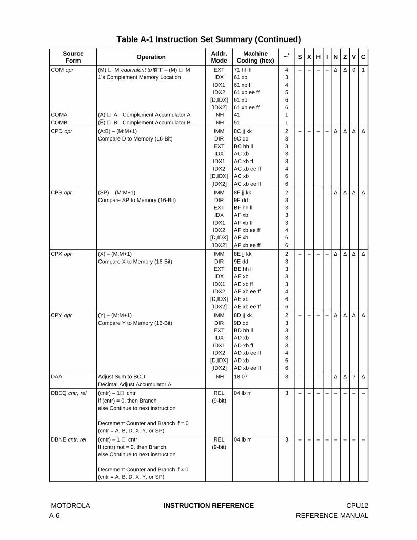
COM opr
COMACOMB
(M) ⇒ M equivalent to $FF – (M) ⇒ M1’s Complement Memory Location
(A) ⇒ A Complement Accumulator A(B) ⇒ B Complement Accumulator B
EXTIDXIDX1IDX2
[D,IDX][IDX2]INHINH
71 hh ll61 xb61 xb ff61 xb ee ff61 xb61 xb ee ff4151
43456611
– – – – ∆ ∆ 0 1
CPD opr (A:B) – (M:M+1)Compare D to Memory (16-Bit)
IMMDIREXTIDXIDX1IDX2
[D,IDX][IDX2]
8C jj kk9C ddBC hh llAC xbAC xb ffAC xb ee ffAC xbAC xb ee ff
23333466
– – – – ∆ ∆ ∆ ∆
CPS opr (SP) – (M:M+1)Compare SP to Memory (16-Bit)
IMMDIREXTIDXIDX1IDX2
[D,IDX][IDX2]
8F jj kk9F ddBF hh llAF xbAF xb ffAF xb ee ffAF xbAF xb ee ff
23333466
– – – – ∆ ∆ ∆ ∆
CPX opr (X) – (M:M+1)Compare X to Memory (16-Bit)
IMMDIREXTIDXIDX1IDX2
[D,IDX][IDX2]
8E jj kk9E ddBE hh llAE xbAE xb ffAE xb ee ffAE xbAE xb ee ff
23333466
– – – – ∆ ∆ ∆ ∆
CPY opr (Y) – (M:M+1)Compare Y to Memory (16-Bit)
IMMDIREXTIDXIDX1IDX2
[D,IDX][IDX2]
8D jj kk9D ddBD hh llAD xbAD xb ffAD xb ee ffAD xbAD xb ee ff
23333466
– – – – ∆ ∆ ∆ ∆
DAA Adjust Sum to BCDDecimal Adjust Accumulator A
INH 18 07 3 – – – – ∆ ∆ ? ∆
DBEQ cntr, rel (cntr) – 1⇒ cntrif (cntr) = 0, then Branchelse Continue to next instruction
Decrement Counter and Branch if = 0(cntr = A, B, D, X, Y, or SP)
REL(9-bit)
04 lb rr 3 – – – – – – – –
DBNE cntr, rel (cntr) – 1 ⇒ cntrIf (cntr) not = 0, then Branch;else Continue to next instruction
Decrement Counter and Branch if ≠ 0(cntr = A, B, D, X, Y, or SP)
REL(9-bit)
04 lb rr 3 – – – – – – – –
Table A-1 Instruction Set Summary (Continued)
SourceForm Operation Addr.
ModeMachine
Coding (hex) ~* S X H I N Z V C
MOTOROLA INSTRUCTION REFERENCE CPU12
A-6 REFERENCE MANUAL

DEC opr
DECADECB
(M) – $01 ⇒ MDecrement Memory Location
(A) – $01 ⇒ A Decrement A(B) – $01 ⇒ B Decrement B
EXTIDXIDX1IDX2
[D,IDX][IDX2]INHINH
73 hh ll63 xb63 xb ff63 xb ee ff63 xb63 xb ee ff4353
43456611
– – – – ∆ ∆ ∆ –
DES (SP) – $0001 ⇒ SPTranslates to LEAS –1,SP
IDX 1B 9F 2 – – – – – – – –
DEX (X) – $0001 ⇒ XDecrement Index Register X
INH 09 1 – – – – – ∆ – –
DEY (Y) – $0001 ⇒ YDecrement Index Register Y
INH 03 1 – – – – – ∆ – –
EDIV (Y:D) ÷ (X) ⇒ Y Remainder ⇒ D32 × 16 Bit ⇒ 16 Bit Divide (unsigned)
INH 11 11 – – – – ∆ ∆ ∆ ∆
EDIVS (Y:D) ÷ (X) ⇒ Y Remainder ⇒ D32 × 16 Bit ⇒ 16 Bit Divide (signed)
INH 18 14 12 – – – – ∆ ∆ ∆ ∆
EMACS sum (M(X):M(X+1)) × (M(Y):M(Y+1)) + (M~M+3) ⇒M~M+3
16 × 16 Bit ⇒ 32 BitMultiply and Accumulate (signed)
Special 18 12 hh ll 13 – – – – ∆ ∆ ∆ ∆
EMAXD opr MAX((D), (M:M+1)) ⇒ DMAX of 2 Unsigned 16-Bit Values
N, Z, V and C status bits reflect result ofinternal compare ((D) – (M:M+1))
IDXIDX1IDX2
[D,IDX][IDX2]
18 1A xb18 1A xb ff18 1A xb ee ff18 1A xb18 1A xb ee ff
44577
– – – – ∆ ∆ ∆ ∆
EMAXM opr MAX((D), (M:M+1)) ⇒ M:M+1MAX of 2 Unsigned 16-Bit Values
N, Z, V and C status bits reflect result ofinternal compare ((D) – (M:M+1))
IDXIDX1IDX2
[D,IDX][IDX2]
18 1E xb18 1E xb ff18 1E xb ee ff18 1E xb18 1E xb ee ff
45677
– – – – ∆ ∆ ∆ ∆
EMIND opr MIN((D), (M:M+1)) ⇒ DMIN of 2 Unsigned 16-Bit Values
N, Z, V and C status bits reflect result ofinternal compare ((D) – (M:M+1))
IDXIDX1IDX2
[D,IDX][IDX2]
18 1B xb18 1B xb ff18 1B xb ee ff18 1B xb18 1B xb ee ff
44577
– – – – ∆ ∆ ∆ ∆
EMINM opr MIN((D), (M:M+1)) ⇒ M:M+1MIN of 2 Unsigned 16-Bit Values
N, Z, V and C status bits reflect result ofinternal compare ((D) – (M:M+1))
IDXIDX1IDX2
[D,IDX][IDX2]
18 1F xb18 1F xb ff18 1F xb ee ff18 1F xb18 1F xb ee ff
45677
– – – – ∆ ∆ ∆ ∆
EMUL (D) × (Y) ⇒ Y:D16 × 16 Bit Multiply (unsigned)
INH 13 3 – – – – ∆ ∆ – ∆
EMULS (D) × (Y) ⇒ Y:D16 × 16 Bit Multiply (signed)
INH 18 13 3 – – – – ∆ ∆ – ∆
Table A-1 Instruction Set Summary (Continued)
SourceForm Operation Addr.
ModeMachine
Coding (hex) ~* S X H I N Z V C
CPU12 INSTRUCTION REFERENCE MOTOROLA
REFERENCE MANUAL A-7

EORA opr (A) ⊕ (M) ⇒ AExclusive-OR A with Memory
IMMDIREXTIDXIDX1IDX2
[D,IDX][IDX2]
88 ii98 ddB8 hh llA8 xbA8 xb ffA8 xb ee ffA8 xbA8 xb ee ff
13333466
– – – – ∆ ∆ 0 –
EORB opr (B) ⊕ (M) ⇒ BExclusive-OR B with Memory
IMMDIREXTIDXIDX1IDX2
[D,IDX][IDX2]
C8 iiD8 ddF8 hh llE8 xbE8 xb ffE8 xb ee ffE8 xbE8 xb ee ff
13333466
– – – – ∆ ∆ 0 –
ETBL opr (M:M+1)+ [(B)×((M+2:M+3) – (M:M+1))] ⇒ D16-Bit Table Lookup and Interpolate
Initialize B, and index before ETBL.<ea> points at first table entry (M:M+1)and B is fractional part of lookup value
(no indirect addr. modes allowed)
IDX 18 3F xb 10 – – – – ∆ ∆ – ?
EXG r1, r2 (r1) ⇔ (r2) (if r1 and r2 same size) or$00:(r1) ⇒ r2 (if r1=8-bit; r2=16-bit) or(r1low) ⇔ (r2) (if r1=16-bit; r2=8-bit)
r1 and r2 may beA, B, CCR, D, X, Y, or SP
INH B7 eb 1 – – – – – – – –
FDIV (D) ÷ (X) ⇒ X; r ⇒ D16 × 16 Bit Fractional Divide
INH 18 11 12 – – – – – ∆ ∆ ∆
IBEQ cntr, rel (cntr) + 1⇒ cntrIf (cntr) = 0, then Branchelse Continue to next instruction
Increment Counter and Branch if = 0(cntr = A, B, D, X, Y, or SP)
REL(9-bit)
04 lb rr 3 – – – – – – – –
IBNE cntr, rel (cntr) + 1⇒ cntrif (cntr) not = 0, then Branch;else Continue to next instruction
Increment Counter and Branch if ≠ 0(cntr = A, B, D, X, Y, or SP)
REL(9-bit)
04 lb rr 3 – – – – – – – –
IDIV (D) ÷ (X) ⇒ X; r ⇒ D16 × 16 Bit Integer Divide (unsigned)
INH 18 10 12 – – – – – ∆ 0 ∆
IDIVS (D) ÷ (X) ⇒ X; r ⇒ D16 × 16 Bit Integer Divide (signed)
INH 18 15 12 – – – – ∆ ∆ ∆ ∆
Table A-1 Instruction Set Summary (Continued)
SourceForm Operation Addr.
ModeMachine
Coding (hex) ~* S X H I N Z V C
MOTOROLA INSTRUCTION REFERENCE CPU12
A-8 REFERENCE MANUAL

INC opr
INCAINCB
(M) + $01 ⇒ MIncrement Memory Byte
(A) + $01 ⇒ A Increment Acc. A(B) + $01 ⇒ B Increment Acc. B
EXTIDXIDX1IDX2
[D,IDX][IDX2]INHINH
72 hh ll62 xb62 xb ff62 xb ee ff62 xb62 xb ee ff4252
43456611
– – – – ∆ ∆ ∆ –
INS (SP) + $0001 ⇒ SPTranslates to LEAS 1,SP
IDX 1B 81 2 – – – – – – – –
INX (X) + $0001 ⇒ XIncrement Index Register X
INH 08 1 – – – – – ∆ – –
INY (Y) + $0001 ⇒ YIncrement Index Register Y
INH 02 1 – – – – – ∆ – –
JMP opr Subroutine address ⇒ PC
Jump
EXTIDXIDX1IDX2
[D,IDX][IDX2]
06 hh ll05 xb05 xb ff05 xb ee ff05 xb05 xb ee ff
333466
– – – – – – – –
JSR opr (SP) – 2 ⇒ SP;RTNH:RTNL ⇒ M(SP):M(SP+1);Subroutine address ⇒ PC
Jump to Subroutine
DIREXTIDXIDX1IDX2
[D,IDX][IDX2]
17 dd16 hh ll15 xb15 xb ff15 xb ee ff15 xb15 xb ee ff
4444577
– – – – – – – –
LBCC rel Long Branch if Carry Clear (if C = 0) REL 18 24 qq rr 4/3 – – – – – – – –
LBCS rel Long Branch if Carry Set (if C = 1) REL 18 25 qq rr 4/3 – – – – – – – –
LBEQ rel Long Branch if Equal (if Z = 1) REL 18 27 qq rr 4/3 – – – – – – – –
LBGE rel Long Branch Greater Than or Equal(if N ⊕ V = 0) (signed)
REL 18 2C qq rr 4/3 – – – – – – – –
LBGT rel Long Branch if Greater Than(if Z ✛ (N ⊕ V) = 0) (signed)
REL 18 2E qq rr 4/3 – – – – – – – –
LBHI rel Long Branch if Higher(if C ✛ Z = 0) (unsigned)
REL 18 22 qq rr 4/3 – – – – – – – –
LBHS rel Long Branch if Higher or Same(if C = 0) (unsigned)same function as LBCC
REL 18 24 qq rr 4/3 – – – – – – – –
LBLE rel Long Branch if Less Than or Equal(if Z ✛ (N ⊕ V) = 1) (signed)
REL 18 2F qq rr 4/3 – – – – – – – –
LBLO rel Long Branch if Lower(if C = 1) (unsigned)same function as LBCS
REL 18 25 qq rr 4/3 – – – – – – – –
LBLS rel Long Branch if Lower or Same(if C ✛ Z = 1) (unsigned)
REL 18 23 qq rr 4/3 – – – – – – – –
LBLT rel Long Branch if Less Than(if N ⊕ V = 1) (signed)
REL 18 2D qq rr 4/3 – – – – – – – –
LBMI rel Long Branch if Minus (if N = 1) REL 18 2B qq rr 4/3 – – – – – – – –
LBNE rel Long Branch if Not Equal (if Z = 0) REL 18 26 qq rr 4/3 – – – – – – – –
LBPL rel Long Branch if Plus (if N = 0) REL 18 2A qq rr 4/3 – – – – – – – –
LBRA rel Long Branch Always (if 1=1) REL 18 20 qq rr 4 – – – – – – – –
Table A-1 Instruction Set Summary (Continued)
SourceForm Operation Addr.
ModeMachine
Coding (hex) ~* S X H I N Z V C
CPU12 INSTRUCTION REFERENCE MOTOROLA
REFERENCE MANUAL A-9

LBRN rel Long Branch Never (if 1 = 0) REL 18 21 qq rr 3 – – – – – – – –
LBVC rel Long Branch if Overflow Bit Clear (if V=0) REL 18 28 qq rr 4/3 – – – – – – – –
LBVS rel Long Branch if Overflow Bit Set (if V = 1) REL 18 29 qq rr 4/3 – – – – – – – –
LDAA opr (M) ⇒ ALoad Accumulator A
IMMDIREXTIDXIDX1IDX2
[D,IDX][IDX2]
86 ii96 ddB6 hh llA6 xbA6 xb ffA6 xb ee ffA6 xbA6 xb ee ff
13333466
– – – – ∆ ∆ 0 –
LDAB opr (M) ⇒ BLoad Accumulator B
IMMDIREXTIDXIDX1IDX2
[D,IDX][IDX2]
C6 iiD6 ddF6 hh llE6 xbE6 xb ffE6 xb ee ffE6 xbE6 xb ee ff
13333466
– – – – ∆ ∆ 0 –
LDD opr (M:M+1) ⇒ A:BLoad Double Accumulator D (A:B)
IMMDIREXTIDXIDX1IDX2
[D,IDX][IDX2]
CC jj kkDC ddFC hh llEC xbEC xb ffEC xb ee ffEC xbEC xb ee ff
23333466
– – – – ∆ ∆ 0 –
LDS opr (M:M+1) ⇒ SPLoad Stack Pointer
IMMDIREXTIDXIDX1IDX2
[D,IDX][IDX2]
CF jj kkDF ddFF hh llEF xbEF xb ffEF xb ee ffEF xbEF xb ee ff
23333466
– – – – ∆ ∆ 0 –
LDX opr (M:M+1) ⇒ XLoad Index Register X
IMMDIREXTIDXIDX1IDX2
[D,IDX][IDX2]
CE jj kkDE ddFE hh llEE xbEE xb ffEE xb ee ffEE xbEE xb ee ff
23333466
– – – – ∆ ∆ 0 –
LDY opr (M:M+1) ⇒ YLoad Index Register Y
IMMDIREXTIDXIDX1IDX2
[D,IDX][IDX2]
CD jj kkDD ddFD hh llED xbED xb ffED xb ee ffED xbED xb ee ff
23333466
– – – – ∆ ∆ 0 –
LEAS opr Effective Address ⇒ SPLoad Effective Address into SP
IDXIDX1IDX2
1B xb1B xb ff1B xb ee ff
222
– – – – – – – –
Table A-1 Instruction Set Summary (Continued)
SourceForm Operation Addr.
ModeMachine
Coding (hex) ~* S X H I N Z V C
MOTOROLA INSTRUCTION REFERENCE CPU12
A-10 REFERENCE MANUAL

LEAX opr Effective Address ⇒ XLoad Effective Address into X
IDXIDX1IDX2
1A xb1A xb ff1A xb ee ff
222
– – – – – – – –
LEAY opr Effective Address ⇒ YLoad Effective Address into Y
IDXIDX1IDX2
19 xb19 xb ff19 xb ee ff
222
– – – – – – – –
LSL opr
LSLALSLB
Logical Shift Leftsame function as ASL
Logical Shift Accumulator A to LeftLogical Shift Accumulator B to Left
EXTIDXIDX1IDX2
[D,IDX][IDX2]INHINH
78 hh ll68 xb68 xb ff68 xb ee ff68 xb68 xb ee ff4858
43456611
– – – – ∆ ∆ ∆ ∆
LSLD
Logical Shift Left D Accumulatorsame function as ASLD
INH 59 1 – – – – ∆ ∆ ∆ ∆
LSR opr
LSRALSRB
Logical Shift Right
Logical Shift Accumulator A to RightLogical Shift Accumulator B to Right
EXTIDXIDX1IDX2
[D,IDX][IDX2]INHINH
74 hh ll64 xb64 xb ff64 xb ee ff64 xb64 xb ee ff4454
43456611
– – – – 0 ∆ ∆ ∆
LSRD
Logical Shift Right D Accumulator
INH 49 1 – – – – 0 ∆ ∆ ∆
MAXA MAX((A), (M)) ⇒ AMAX of 2 Unsigned 8-Bit Values
N, Z, V and C status bits reflect result ofinternal compare ((A) – (M)).
IDXIDX1IDX2
[D,IDX][IDX2]
18 18 xb18 18 xb ff18 18 xb ee ff18 18 xb18 18 xb ee ff
44577
– – – – ∆ ∆ ∆ ∆
MAXM MAX((A), (M)) ⇒ MMAX of 2 Unsigned 8-Bit Values
N, Z, V and C status bits reflect result ofinternal compare ((A) – (M)).
IDXIDX1IDX2
[D,IDX][IDX2]
18 1C xb18 1C xb ff18 1C xb ee ff18 1C xb18 1C xb ee ff
45677
– – – – ∆ ∆ ∆ ∆
MEM µ (grade) ⇒ M(Y);(X) + 4 ⇒ X; (Y) + 1 ⇒ Y; A unchanged
if (A) < P1 or (A) > P2 then µ = 0, elseµ = MIN[((A) – P1)×S1, (P2 – (A))×S2, $FF]where:A = current crisp input value;X points at 4-byte data structure that de-scribes a trapezoidal membership function(P1, P2, S1, S2);Y points at fuzzy input (RAM location).See instruction details for special cases.
Special 01 5 – – ? – ? ? ? ?
Table A-1 Instruction Set Summary (Continued)
SourceForm Operation Addr.
ModeMachine
Coding (hex) ~* S X H I N Z V C
C0
b7 b0
C0
b7 b0A Bb7b0
C0
b7 b0
C0
b7 b0A Bb7b0
CPU12 INSTRUCTION REFERENCE MOTOROLA
REFERENCE MANUAL A-11

MINA MIN((A), (M)) ⇒ AMIN of Two Unsigned 8-Bit Values
N, Z, V and C status bits reflect result ofinternal compare ((A) – (M)).
IDXIDX1IDX2
[D,IDX][IDX2]
18 19 xb18 19 xb ff18 19 xb ee ff18 19 xb18 19 xb ee ff
44577
– – – – ∆ ∆ ∆ ∆
MINM MIN((A), (M)) ⇒ MMIN of Two Unsigned 8-Bit Values
N, Z, V and C status bits reflect result ofinternal compare ((A) – (M)).
IDXIDX1IDX2
[D,IDX][IDX2]
18 1D xb18 1D xb ff18 1D xb ee ff18 1D xb18 1D xb ee ff
45677
– – – – ∆ ∆ ∆ ∆
MOVB opr1, opr2 (M1) ⇒ M2Memory to Memory Byte-Move (8-Bit)
IMM-EXTIMM-IDXEXT-EXTEXT-IDXIDX-EXTIDX-IDX
18 0B ii hh ll18 08 xb ii18 0C hh ll hh ll18 09 xb hh ll18 0D xb hh ll18 0A xb xb
446555
– – – – – – – –
MOVW opr1, opr2 (M:M+11) ⇒ M:M+12Memory to Memory Word-Move (16-Bit)
IMM-EXTIMM-IDXEXT-EXTEXT-IDXIDX-EXTIDX-IDX
18 03 jj kk hh ll18 00 xb jj kk18 04 hh ll hh ll18 01 xb hh ll18 05 xb hh ll18 02 xb xb
546555
– – – – – – – –
MUL (A) × (B) ⇒ A:B
8 × 8 Unsigned Multiply
INH 12 3 – – – – – – – ∆
NEG opr
NEGA
NEGB
0 – (M) ⇒ M or (M) + 1 ⇒ MTwo’s Complement Negate
0 – (A) ⇒ A equivalent to (A) + 1 ⇒ BNegate Accumulator A0 – (B) ⇒ B equivalent to (B) + 1 ⇒ BNegate Accumulator B
EXTIDXIDX1IDX2
[D,IDX][IDX2]INH
INH
70 hh ll60 xb60 xb ff60 xb ee ff60 xb60 xb ee ff40
50
4345661
1
– – – – ∆ ∆ ∆ ∆
NOP No Operation INH A7 1 – – – – – – – –
ORAA opr (A) ✛ (M) ⇒ ALogical OR A with Memory
IMMDIREXTIDXIDX1IDX2
[D,IDX][IDX2]
8A ii9A ddBA hh llAA xbAA xb ffAA xb ee ffAA xbAA xb ee ff
13333466
– – – – ∆ ∆ 0 –
ORAB opr (B) ✛ (M) ⇒ BLogical OR B with Memory
IMMDIREXTIDXIDX1IDX2
[D,IDX][IDX2]
CA iiDA ddFA hh llEA xbEA xb ffEA xb ee ffEA xbEA xb ee ff
13333466
– – – – ∆ ∆ 0 –
ORCC opr (CCR) ✛ M ⇒ CCRLogical OR CCR with Memory
IMM 14 ii 1 ⇑ – ⇑ ⇑ ⇑ ⇑ ⇑ ⇑
Table A-1 Instruction Set Summary (Continued)
SourceForm Operation Addr.
ModeMachine
Coding (hex) ~* S X H I N Z V C
MOTOROLA INSTRUCTION REFERENCE CPU12
A-12 REFERENCE MANUAL

PSHA (SP) – 1 ⇒ SP; (A) ⇒ M(SP)
Push Accumulator A onto Stack
INH 36 2 – – – – – – – –
PSHB (SP) – 1 ⇒ SP; (B) ⇒ M(SP)
Push Accumulator B onto Stack
INH 37 2 – – – – – – – –
PSHC (SP) – 1 ⇒ SP; (CCR) ⇒ M(SP)
Push CCR onto Stack
INH 39 2 – – – – – – – –
PSHD (SP) – 2 ⇒ SP; (A:B) ⇒ M(SP):M(SP+1)
Push D Accumulator onto Stack
INH 3B 2 – – – – – – – –
PSHX (SP) – 2 ⇒ SP; (XH:XL) ⇒ M(SP):M(SP+1)
Push Index Register X onto Stack
INH 34 2 – – – – – – – –
PSHY (SP) – 2 ⇒ SP; (YH:YL) ⇒ M(SP):M(SP+1)
Push Index Register Y onto Stack
INH 35 2 – – – – – – – –
PULA (M(SP)) ⇒ A; (SP) + 1 ⇒ SP
Pull Accumulator A from Stack
INH 32 3 – – – – – – – –
PULB (M(SP)) ⇒ B; (SP) + 1 ⇒ SP
Pull Accumulator B from Stack
INH 33 3 – – – – – – – –
PULC (M(SP)) ⇒ CCR; (SP) + 1 ⇒ SP
Pull CCR from Stack
INH 38 3 ∆ ⇓ ∆ ∆ ∆ ∆ ∆ ∆
PULD (M(SP):M(SP+1)) ⇒ A:B; (SP) + 2 ⇒ SP
Pull D from Stack
INH 3A 3 – – – – – – – –
PULX (M(SP):M(SP+1)) ⇒ XH:XL; (SP) + 2 ⇒ SP
Pull Index Register X from Stack
INH 30 3 – – – – – – – –
PULY (M(SP):M(SP+1)) ⇒ YH:YL; (SP) + 2 ⇒ SP
Pull Index Register Y from Stack
INH 31 3 – – – – – – – –
REV MIN-MAX rule evaluationFind smallest rule input (MIN).Store to rule outputs unless fuzzy output isalready larger (MAX).
For rule weights see REVW.
Each rule input is an 8-bit offset from thebase address in Y. Each rule output is an 8-bit offset from the base address in Y. $FEseparates rule inputs from rule outputs. $FFterminates the rule list.
REV may be interrupted.
Special 18 3A 3**
perrulebyte
– – – – – – ∆ –
Table A-1 Instruction Set Summary (Continued)
SourceForm Operation Addr.
ModeMachine
Coding (hex) ~* S X H I N Z V C
CPU12 INSTRUCTION REFERENCE MOTOROLA
REFERENCE MANUAL A-13

REVW MIN-MAX rule evaluationFind smallest rule input (MIN),Store to rule outputs unless fuzzy output isalready larger (MAX).
Rule weights supported, optional.
Each rule input is the 16-bit address of afuzzy input. Each rule output is the 16-bit ad-dress of a fuzzy output. The value $FFFEseparates rule inputs from rule outputs.$FFFF terminates the rule list.
REVW may be interrupted.
Special 18 3B 3**
perrulebyte;
5perwt.
– – ? – ? ? ∆ !
ROL opr
ROLAROLB
Rotate Memory Left through Carry
Rotate A Left through CarryRotate B Left through Carry
EXTIDXIDX1IDX2
[D,IDX][IDX2]INHINH
75 hh ll65 xb65 xb ff65 xb ee ff65 xb65 xb ee ff4555
43456611
– – – – ∆ ∆ ∆ ∆
ROR opr
RORARORB
Rotate Memory Right through Carry
Rotate A Right through CarryRotate B Right through Carry
EXTIDXIDX1IDX2
[D,IDX][IDX2]INHINH
76 hh ll66 xb66 xb ff66 xb ee ff66 xb66 xb ee ff4656
43456611
– – – – ∆ ∆ ∆ ∆
RTC (M(SP)) ⇒ PPAGE; (SP) + 1 ⇒ SP;(M(SP):M(SP+1)) ⇒ PCH:PCL;(SP) + 2 ⇒ SP
Return from Call
INH 0A 6 – – – – – – – –
RTI (M(SP)) ⇒ CCR; (SP) + 1 ⇒ SP(M(SP):M(SP+1)) ⇒ B:A; (SP) + 2 ⇒ SP(M(SP):M(SP+1)) ⇒ XH:XL; (SP) + 4 ⇒ SP(M(SP):M(SP+1)) ⇒ PCH:PCL; (SP) – 2 ⇒ SP(M(SP):M(SP+1)) ⇒ YH:YL;(SP) + 4 ⇒ SP
Return from Interrupt
INH 0B 8 ∆ ⇓ ∆ ∆ ∆ ∆ ∆ ∆
RTS (M(SP):M(SP+1)) ⇒ PCH:PCL;(SP) + 2 ⇒ SP
Return from Subroutine
INH 3D 5 – – – – – – – –
SBA (A) – (B) ⇒ ASubtract B from A
INH 18 16 2 – – – – ∆ ∆ ∆ ∆
Table A-1 Instruction Set Summary (Continued)
SourceForm Operation Addr.
ModeMachine
Coding (hex) ~* S X H I N Z V C
C b7 b0
Cb7 b0
MOTOROLA INSTRUCTION REFERENCE CPU12
A-14 REFERENCE MANUAL

SBCA opr (A) – (M) – C ⇒ ASubtract with Borrow from A
IMMDIREXTIDXIDX1IDX2
[D,IDX][IDX2]
82 ii92 ddB2 hh llA2 xbA2 xb ffA2 xb ee ffA2 xbA2 xb ee ff
13333466
– – – – ∆ ∆ ∆ ∆
SBCB opr (B) – (M) – C ⇒ BSubtract with Borrow from B
IMMDIREXTIDXIDX1IDX2
[D,IDX][IDX2]
C2 iiD2 ddF2 hh llE2 xbE2 xb ffE2 xb ee ffE2 xbE2 xb ee ff
13333466
– – – – ∆ ∆ ∆ ∆
SEC 1 ⇒ CTranslates to ORCC #$01
IMM 14 01 1 – – – – – – – 1
SEI 1 ⇒ I; (inhibit I interrupts)Translates to ORCC #$10
IMM 14 10 1 – – – 1 – – – –
SEV 1 ⇒ VTranslates to ORCC #$02
IMM 14 02 1 – – – – – – 1 –
SEX r1, r2 $00:(r1) ⇒ r2 if r1, bit 7 is 0 or$FF:(r1) ⇒ r2 if r1, bit 7 is 1
Sign Extend 8-bit r1 to 16-bit r2r1 may be A, B, or CCRr2 may be D, X, Y, or SP
Alternate mnemonic for TFR r1, r2
INH B7 eb 1 – – – – – – – –
STAA opr (A) ⇒ MStore Accumulator A to Memory
DIREXTIDXIDX1IDX2
[D,IDX][IDX2]
5A dd7A hh ll6A xb6A xb ff6A xb ee ff6A xb6A xb ee ff
2323355
– – – – ∆ ∆ 0 –
STAB opr (B) ⇒ MStore Accumulator B to Memory
DIREXTIDXIDX1IDX2
[D,IDX][IDX2]
5B dd7B hh ll6B xb6B xb ff6B xb ee ff6B xb6B xb ee ff
2323355
– – – – ∆ ∆ 0 –
STD opr (A) ⇒ M, (B) ⇒ M+1Store Double Accumulator
DIREXTIDXIDX1IDX2
[D,IDX][IDX2]
5C dd7C hh ll6C xb6C xb ff6C xb ee ff6C xb6C xb ee ff
2323355
– – – – ∆ ∆ 0 –
Table A-1 Instruction Set Summary (Continued)
SourceForm Operation Addr.
ModeMachine
Coding (hex) ~* S X H I N Z V C
CPU12 INSTRUCTION REFERENCE MOTOROLA
REFERENCE MANUAL A-15

STOP (SP) – 2 ⇒ SP;RTNH:RTNL ⇒ M(SP):M(SP+1);(SP) – 2 ⇒ SP; (YH:YL) ⇒ M(SP):M(SP+1);(SP) – 2 ⇒ SP; (XH:XL) ⇒ M(SP):M(SP+1);(SP) – 2 ⇒ SP; (B:A) ⇒ M(SP):M(SP+1);(SP) – 1 ⇒ SP; (CCR) ⇒ M(SP);STOP All Clocks
If S control bit = 1, the STOP instruction isdisabled and acts like a two-cycle NOP.
Registers stacked to allow quicker recoveryby interrupt.
INH 18 3E 9**
+5or
+2**
– – – – – – – –
STS opr (SPH:SPL) ⇒ M:M+1Store Stack Pointer
DIREXTIDXIDX1IDX2
[D,IDX][IDX2]
5F dd7F hh ll6F xb6F xb ff6F xb ee ff6F xb6F xb ee ff
2323355
– – – – ∆ ∆ 0 –
STX opr (XH:XL) ⇒ M:M+1Store Index Register X
DIREXTIDXIDX1IDX2
[D,IDX][IDX2]
5E dd7E hh ll6E xb6E xb ff6E xb ee ff6E xb6E xb ee ff
2323355
– – – – ∆ ∆ 0 –
STY opr (YH:YL) ⇒ M:M+1Store Index Register Y
DIREXTIDXIDX1IDX2
[D,IDX][IDX2]
5D dd7D hh ll6D xb6D xb ff6D xb ee ff6D xb6D xb ee ff
2323355
– – – – ∆ ∆ 0 –
SUBA opr (A) – (M) ⇒ ASubtract Memory from Accumulator A
IMMDIREXTIDXIDX1IDX2
[D,IDX][IDX2]
80 ii90 ddB0 hh llA0 xbA0 xb ffA0 xb ee ffA0 xbA0 xb ee ff
13333466
– – – – ∆ ∆ ∆ ∆
SUBB opr (B) – (M) ⇒ BSubtract Memory from Accumulator B
IMMDIREXTIDXIDX1IDX2
[D,IDX][IDX2]
C0 iiD0 ddF0 hh llE0 xbE0 xb ffE0 xb ee ffE0 xbE0 xb ee ff
13333466
– – – – ∆ ∆ ∆ ∆
Table A-1 Instruction Set Summary (Continued)
SourceForm Operation Addr.
ModeMachine
Coding (hex) ~* S X H I N Z V C
MOTOROLA INSTRUCTION REFERENCE CPU12
A-16 REFERENCE MANUAL
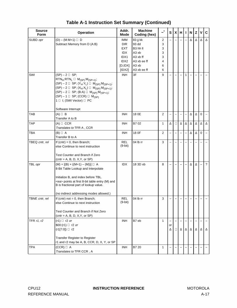
SUBD opr (D) – (M:M+1) ⇒ DSubtract Memory from D (A:B)
IMMDIREXTIDXIDX1IDX2
[D,IDX][IDX2]
83 jj kk93 ddB3 hh llA3 xbA3 xb ffA3 xb ee ffA3 xbA3 xb ee ff
23333466
– – – – ∆ ∆ ∆ ∆
SWI (SP) – 2 ⇒ SP;RTNH:RTNL ⇒ M(SP):M(SP+1);(SP) – 2 ⇒ SP; (YH:YL) ⇒ M(SP):M(SP+1);(SP) – 2 ⇒ SP; (XH:XL) ⇒ M(SP):M(SP+1);(SP) – 2 ⇒ SP; (B:A) ⇒ M(SP):M(SP+1);(SP) – 1 ⇒ SP; (CCR) ⇒ M(SP)1 ⇒ I; (SWI Vector) ⇒ PC
Software Interrupt
INH 3F 9 – – – 1 – – – –
TAB (A) ⇒ BTransfer A to B
INH 18 0E 2 – – – – ∆ ∆ 0 –
TAP (A) ⇒ CCRTranslates to TFR A , CCR
INH B7 02 1 ∆ ⇓ ∆ ∆ ∆ ∆ ∆ ∆
TBA (B) ⇒ ATransfer B to A
INH 18 0F 2 – – – – ∆ ∆ 0 –
TBEQ cntr, rel If (cntr) = 0, then Branch;else Continue to next instruction
Test Counter and Branch if Zero(cntr = A, B, D, X,Y, or SP)
REL(9-bit)
04 lb rr 3 – – – – – – – –
TBL opr (M) + [(B) × ((M+1) – (M))] ⇒ A8-Bit Table Lookup and Interpolate
Initialize B, and index before TBL.<ea> points at first 8-bit table entry (M) andB is fractional part of lookup value.
(no indirect addressing modes allowed.)
IDX 18 3D xb 8 – – – – ∆ ∆ – ?
TBNE cntr, rel If (cntr) not = 0, then Branch;else Continue to next instruction
Test Counter and Branch if Not Zero(cntr = A, B, D, X,Y, or SP)
REL(9-bit)
04 lb rr 3 – – – – – – – –
TFR r1, r2 (r1) ⇒ r2 or$00:(r1) ⇒ r2 or(r1[7:0]) ⇒ r2
Transfer Register to Registerr1 and r2 may be A, B, CCR, D, X, Y, or SP
INH B7 eb 1 –or∆
–
⇓
–
∆
–
∆
–
∆
–
∆
–
∆
–
∆
TPA (CCR) ⇒ ATranslates to TFR CCR , A
INH B7 20 1 – – – – – – – –
Table A-1 Instruction Set Summary (Continued)
SourceForm Operation Addr.
ModeMachine
Coding (hex) ~* S X H I N Z V C
CPU12 INSTRUCTION REFERENCE MOTOROLA
REFERENCE MANUAL A-17

TRAP (SP) – 2 ⇒ SP;RTNH:RTNL ⇒ M(SP):M(SP+1);(SP) – 2 ⇒ SP; (YH:YL) ⇒ M(SP):M(SP+1);(SP) – 2 ⇒ SP; (XH:XL) ⇒ M(SP):M(SP+1);(SP) – 2 ⇒ SP; (B:A) ⇒ M(SP):M(SP+1);(SP) – 1 ⇒ SP; (CCR) ⇒ M(SP)1 ⇒ I; (TRAP Vector) ⇒ PC
Unimplemented opcode trap
INH 18 tntn = $30–$39
or$40–$FF
10 – – – 1 – – – –
TST opr
TSTATSTB
(M) – 0Test Memory for Zero or Minus
(A) – 0 Test A for Zero or Minus(B) – 0 Test B for Zero or Minus
EXTIDXIDX1IDX2
[D,IDX][IDX2]INHINH
F7 hh llE7 xbE7 xb ffE7 xb ee ffE7 xbE7 xb ee ff97D7
33346611
– – – – ∆ ∆ 0 0
TSX (SP) ⇒ XTranslates to TFR SP,X
INH B7 75 1 – – – – – – – –
TSY (SP) ⇒ YTranslates to TFR SP,Y
INH B7 76 1 – – – – – – – –
TXS (X) ⇒ SPTranslates to TFR X,SP
INH B7 57 1 – – – – – – – –
TYS (Y) ⇒ SPTranslates to TFR Y,SP
INH B7 67 1 – – – – – – – –
WAI (SP) – 2 ⇒ SP;RTNH:RTNL ⇒ M(SP):M(SP+1);(SP) – 2 ⇒ SP; (YH:YL) ⇒ M(SP):M(SP+1);(SP) – 2 ⇒ SP; (XH:XL) ⇒ M(SP):M(SP+1);(SP) – 2 ⇒ SP; (B:A) ⇒ M(SP):M(SP+1);(SP) – 1 ⇒ SP; (CCR) ⇒ M(SP);
WAIT for interrupt
INH 3E 8**
(in)+5
(int)
–or–or–
–
–
1
–
–
–
–
1
1
–
–
–
–
–
–
–
–
–
–
–
–
WAV
Calculate Sum of Products and Sum ofWeights for Weighted Average Calculation
Initialize B, X, and Y before WAV. B specifiesnumber of elements. X points at first elementin Si list. Y points at first element in Fi list.
All Si and Fi elements are 8-bits.
If interrupted, six extra bytes of stack usedfor intermediate values
Special 18 3C 8**
perlable
– – ? – ? ∆ ? ?
Table A-1 Instruction Set Summary (Continued)
SourceForm Operation Addr.
ModeMachine
Coding (hex) ~* S X H I N Z V C
F ii 1=
B
∑ X⇒
Si F ii 1=
B
∑ Y:D⇒
MOTOROLA INSTRUCTION REFERENCE CPU12
A-18 REFERENCE MANUAL

Key to Table A-2
Addressing mode abbreviations:
DI — DirectEX — ExtendedID — IndexedIH — InherentIM — ImmediateRL — RelativeSP — Special
Cycle counts are for single-chip mode with 16-bit internal buses. Stack location (internal or external),external bus width, and operand alignment can affect actual execution time.
wavr
pseudo-instruction
see WAV
Resume executing an interrupted WAV in-struction (recover intermediate results fromstack rather than initializing them to zero)
Special 3C ** – – ? – ? ∆ ? ?
XGDX (D) ⇔ (X)Translates to EXG D, X
INH B7 C5 1 – – – – – – – –
XGDY (D) ⇔ (Y)Translates to EXG D, Y
INH B7 C6 1 – – – – – – – –
NOTES:*Each cycle (~) is typically 125 ns for an 8-MHz bus (16-MHz oscillator).**Refer to detailed instruction descriptions for additional information.
Table A-1 Instruction Set Summary (Continued)
SourceForm Operation Addr.
ModeMachine
Coding (hex) ~* S X H I N Z V C
opcode (hex)
addressing mode
mnemonic
cycle count
00 0
0AA
MNE
byte count
CPU12 INSTRUCTION REFERENCE MOTOROLA
REFERENCE MANUAL A-19

MO
TO
RO
LAIN
ST
RU
CT
ION
RE
FE
RE
NC
EC
PU
12
A-20
RE
FE
RE
NC
E M
AN
UA
L
0 1SUBBM 2
D0 3SUBB
DI 2
E0 3-6SUBB
ID 2-4
F0 3SUBB
EX 31 1CMPBM 2
D1 3CMPB
DI 2
E1 3-6CMPB
ID 2-4
F1 3CMPB
EX 32 1SBCBM 2
D2 3SBCB
DI 2
E2 3-6SBCB
ID 2-4
F2 3SBCB
EX 33 2ADDDM 3
D3 3ADDD
DI 2
E3 3-6ADDD
ID 2-4
F3 3ADDD
EX 34 1ANDBM 2
D4 3ANDB
DI 2
E4 3-6ANDB
ID 2-4
F4 3ANDB
EX 35 1BITB
M 2
D5 3BITB
DI 2
E5 3-6BITB
ID 2-4
F5 3BITB
EX 36 1LDAB
M 2
D6 3LDAB
DI 2
E6 3-6LDAB
ID 2-4
F6 3LDAB
EX 37 1CLRBH 1
D7 1TSTB
IH 1
E7 3-6TST
ID 2-4
F7 3TST
EX 38 1EORBM 2
D8 3EORB
DI 2
E8 3-6EORB
ID 2-4
F8 3EORB
EX 39 1ADCBM 2
D9 3ADCB
DI 2
E9 3-6ADCB
ID 2-4
F9 3ADCB
EX 3A 1ORABM 2
DA 3ORAB
DI 2
EA 3-6ORAB
ID 2-4
FA 3ORAB
EX 3B 1ADDBM 2
DB 3ADDB
DI 2
EB 3-6ADDB
ID 2-4
FB 3ADDB
EX 3C 2LDD
M 3
DC 3LDD
DI 2
EC 3-6LDD
ID 2-4
FC 3LDD
EX 3CD 2
LDYIM 3
DD 3LDY
DI 2
ED 3-6LDY
ID 2-4
FD 3LDY
EX 3CE 2
LDXIM 3
DE 3LDX
DI 2
EE 3-6LDX
ID 2-4
FE 3LDX
EX 3CF 2
LDSIM 3
DF 3LDS
DI 2
EF 3-6LDS
ID 2-4
FF 3LDS
EX 3
Table A-2 CPU12 Opcode Map (Sheet 1 of 2)00 *5BGND
IH 1
10 1ANDCCIM 2
20 3BRA
RL 2
30 3PULX
IH 1
40 1NEGA
IH 1
50 1NEGB
IH 1
60 3-6NEG
ID 2-4
70 4NEG
EX 3
80 1SUBA
IM 2
90 3SUBA
DI 2
A0 3-6SUBA
ID 2-4
B0 3SUBA
EX 3
C
I01 5
MEMIH 1
11 11EDIV
IH 1
21 1BRN
RL 2
31 3PULY
IH 1
41 1COMA
IH 1
51 1COMB
IH 1
61 3-6COM
ID 2-4
71 4COM
EX 3
81 1CMPA
IM 2
91 3CMPA
DI 2
A1 3-6CMPA
ID 2-4
B1 3CMPA
EX 3
C
I02 1
INYIH 1
12 3MUL
IH 1
22 3/1BHI
RL 2
32 3PULA
IH 1
42 1INCA
IH 1
52 1INCB
IH 1
62 3-6INC
ID 2-4
72 4INC
EX 3
82 1SBCA
IM 2
92 3SBCA
DI 2
A2 3-6SBCA
ID 2-4
B2 3SBCA
EX 3
C
I03 1
DEYIH 1
13 3EMUL
IH 1
23 3/1BLS
RL 2
33 3PULB
IH 1
43 1DECA
IH 1
53 1DECB
IH 1
63 3-6DEC
ID 2-4
73 4DEC
EX 3
83 2SUBD
IM 3
93 3SUBD
DI 2
A3 3-6SUBD
ID 2-4
B3 3SUBD
EX 3
C
I04 3
loop‡
RL 3
14 1ORCC
IM 2
24 3/1BCC
RL 2
34 2PSHX
IH 1
44 1LSRA
IH 1
54 1LSRB
IH 1
64 3-6LSR
ID 2-4
74 4LSR
EX 3
84 1ANDA
IM 2
94 3ANDA
DI 2
A4 3-6ANDA
ID 2-4
B4 3ANDA
EX 3
C
I05 3-6
JMPID 2-4
15 4-7JSR
ID 2-4
25 3/1BCS
RL 2
35 2PSHY
IH 1
45 1ROLA
IH 1
55 1ROLB
IH 1
65 3-6ROL
ID 2-4
75 4ROL
EX 3
85 1BITA
IM 2
95 3BITA
DI 2
A5 3-6BITA
ID 2-4
B5 3BITA
EX 3
C
I06 3
JMPEX 3
16 4JSR
EX 3
26 3/1BNE
RL 2
36 2PSHA
IH 1
46 1RORA
IH 1
56 1RORB
IH 1
66 3-6ROR
ID 2-4
76 4ROR
EX 3
86 1LDAA
IM 2
96 3LDAA
DI 2
A6 3-6LDAA
ID 2-4
B6 3LDAA
EX 3
C
I07 4
BSRRL 2
17 4JSR
DI 2
27 3/1BEQ
RL 2
37 2PSHB
IH 1
47 1ASRA
IH 1
57 1ASRB
IH 1
67 3-6ASR
ID 2-4
77 4ASR
EX 3
87 1CLRA
IH 1
97 1TSTA
IH 1
A7 1NOP
IH 1
B7 1TFR/EXGIH 2
C
I08 1
INXIH 1
18 -page 2
- -
28 3/1BVC
RL 2
38 3PULC
IH 1
48 1ASLA
IH 1
58 1ASLB
IH 1
68 3-6ASL
ID 2-4
78 4ASL
EX 3
88 1EORA
IM 2
98 3EORA
DI 2
A8 3-6EORA
ID 2-4
B8 3EORA
EX 3
C
I09 1
DEXIH 1
19 2LEAY
ID 2-4
29 3/1BVS
RL 2
39 2PSHC
IH 1
49 1LSRD
IH 1
59 1ASLD
IH 1
69 2-5CLR
ID 2-4
79 3CLR
EX 3
89 1ADCA
IM 2
99 3ADCA
DI 2
A9 3-6ADCA
ID 2-4
B9 3ADCA
EX 3
C
I0A 6
RTCIH 1
1A 2LEAX
ID 2-4
2A 3/1BPL
RL 2
3A 3PULD
IH 1
4A 8CALL
EX 4
5A 2STAA
DI 2
6A 2-5STAA
ID 2-4
7A 3STAA
EX 3
8A 1ORAA
IM 2
9A 3ORAA
DI 2
AA 3-6ORAA
ID 2-4
BA 3ORAA
EX 3
C
I0B 8
RTIIH 1
1B 2LEAS
ID 2-4
2B 3/1BMI
RL 2
3B 2PSHD
IH 1
4B 8-10CALL
ID 2-5
5B 2STAB
DI 2
6B 2-5STAB
ID 2-4
7B 3STAB
EX 3
8B 1ADDA
IM 2
9B 3ADDA
DI 2
AB 3-6ADDA
ID 2-4
BB 3ADDA
EX 3
C
I0C 4-6BSET
ID 3-5
1C 4BSET
EX 4
2C 3/1BGE
RL 2
3C *+9wavr
SP 1
4C 4BSET
DI 3
5C 2STD
DI 2
6C 2-5STD
ID 2-4
7C 3STD
EX 3
8C 2CPD
IM 3
9C 3CPD
DI 2
AC 3-6CPD
ID 2-4
BC 3CPD
EX 3
C
I0D 4-6BCLR
ID 3-5
1D 4BCLR
EX 4
2D 3/1BLT
RL 2
3D 5RTS
IH 1
4D 4BCLR
DI 3
5D 2STY
DI 2
6D 2-5STY
ID 2-4
7D 3STY
EX 3
8D 2CPY
IM 3
9D 3CPY
DI 2
AD 3-6CPY
ID 2-4
BD 3CPY
EX 30E 4-8BRSETID 4-6
1E 5BRSETEX 5
2E 3/1BGT
RL 2
3E *8WAI
IH 1
4E 4BRSETDI 4
5E 2STX
DI 2
6E 2-5STX
ID 2-4
7E 3STX
EX 3
8E 2CPX
IM 3
9E 3CPX
DI 2
AE 3-6CPX
ID 2-4
BE 3CPX
EX 30F 4-8BRCLRID 4-6
1F 5BRCLREX 5
2F 3/1BLE
RL 2
3F 9SWI
IH 1
4F 4BRCLRDI 4
5F 2STS
DI 2
6F 2-5STS
ID 2-4
7F 3STS
EX 3
8F 2CPS
IM 3
9F 3CPS
DI 2
AF 3-6CPS
ID 2-4
BF 3CPS
EX 3

CP
U12
INS
TR
UC
TIO
N R
EF
ER
EN
CE
MO
TO
RO
LA
RE
FE
RE
NC
E M
AN
UA
LA
-21 NE.
10AP
2
D0 10TRAP
IH 2
E0 10TRAP
IH 2
F0 10TRAP
IH 210
AP2
D1 10TRAP
IH 2
E1 10TRAP
IH 2
F1 10TRAP
IH 210
AP2
D2 10TRAP
IH 2
E2 10TRAP
IH 2
F2 10TRAP
IH 210
AP2
D3 10TRAP
IH 2
E3 10TRAP
IH 2
F3 10TRAP
IH 210
AP2
D4 10TRAP
IH 2
E4 10TRAP
IH 2
F4 10TRAP
IH 210
AP2
D5 10TRAP
IH 2
E5 10TRAP
IH 2
F5 10TRAP
IH 210
AP2
D6 10TRAP
IH 2
E6 10TRAP
IH 2
F6 10TRAP
IH 210
AP2
D7 10TRAP
IH 2
E7 10TRAP
IH 2
F7 10TRAP
IH 210
AP2
D8 10TRAP
IH 2
E8 10TRAP
IH 2
F8 10TRAP
IH 210
AP2
D9 10TRAP
IH 2
E9 10TRAP
IH 2
F9 10TRAP
IH 210
AP2
DA 10TRAP
IH 2
EA 10TRAP
IH 2
FA 10TRAP
IH 210
AP2
DB 10TRAP
IH 2
EB 10TRAP
IH 2
FB 10TRAP
IH 210
AP2
DC 10TRAP
IH 2
EC 10TRAP
IH 2
FC 10TRAP
IH 210
AP2
DD 10TRAP
IH 2
ED 10TRAP
IH 2
FD 10TRAP
IH 210
AP2
DE 10TRAP
IH 2
EE 10TRAP
IH 2
FE 10TRAP
IH 210
AP2
DF 10TRAP
IH 2
EF 10TRAP
IH 2
FF 10TRAP
IH 2
* Refer to instruction glossary for more information.‡ The opcode $04 corresponds to one of the loop primitive instructions DBEQ, DBNE, IBEQ, IBNE, TBEQ, or TB
00 4MOVWIM-ID 5
10 12IDIV
IH 2
20 4LBRA
RL 4
30 10TRAP
IH 2
40 10TRAP
IH 2
50 10TRAP
IH 2
60 10TRAP
IH 2
70 10TRAP
IH 2
80 10TRAP
IH 2
90 10TRAP
IH 2
A0 10TRAP
IH 2
B0 10TRAP
IH 2
C0TR
IH01 5MOVWEX-ID 5
11 12FDIV
IH 2
21 3LBRN
RL 4
31 10TRAP
IH 2
41 10TRAP
IH 2
51 10TRAP
IH 2
61 10TRAP
IH 2
71 10TRAP
IH 2
81 10TRAP
IH 2
91 10TRAP
IH 2
A1 10TRAP
IH 2
B1 10TRAP
IH 2
C1TR
IH02 5MOVWID-ID 4
12 13EMACSSP 4
22 4/3LBHI
RL 4
32 10TRAP
IH 2
42 10TRAP
IH 2
52 10TRAP
IH 2
62 10TRAP
IH 2
72 10TRAP
IH 2
82 10TRAP
IH 2
92 10TRAP
IH 2
A2 10TRAP
IH 2
B2 10TRAP
IH 2
C2TR
IH03 5MOVWIM-EX 6
13 3EMULSIH 2
23 4/3LBLS
RL 4
33 10TRAP
IH 2
43 10TRAP
IH 2
53 10TRAP
IH 2
63 10TRAP
IH 2
73 10TRAP
IH 2
83 10TRAP
IH 2
93 10TRAP
IH 2
A3 10TRAP
IH 2
B3 10TRAP
IH 2
C3TR
IH04 6MOVWEX-EX 6
14 12EDIVS
IH 2
24 4/3LBCC
RL 4
34 10TRAP
IH 2
44 10TRAP
IH 2
54 10TRAP
IH 2
64 10TRAP
IH 2
74 10TRAP
IH 2
84 10TRAP
IH 2
94 10TRAP
IH 2
A4 10TRAP
IH 2
B4 10TRAP
IH 2
C4TR
IH05 5MOVWID-EX 5
15 12IDIVS
IH 2
25 4/3LBCS
RL 4
35 10TRAP
IH 2
45 10TRAP
IH 2
55 10TRAP
IH 2
65 10TRAP
IH 2
75 10TRAP
IH 2
85 10TRAP
IH 2
95 10TRAP
IH 2
A5 10TRAP
IH 2
B5 10TRAP
IH 2
C5TR
IH06 2
ABAIH 2
16 2SBA
IH 2
26 4/3LBNE
RL 4
36 10TRAP
IH 2
46 10TRAP
IH 2
56 10TRAP
IH 2
66 10TRAP
IH 2
76 10TRAP
IH 2
86 10TRAP
IH 2
96 10TRAP
IH 2
A6 10TRAP
IH 2
B6 10TRAP
IH 2
C6TR
IH07 3
DAAIH 2
17 2CBA
IH 2
27 4/3LBEQ
RL 4
37 10TRAP
IH 2
47 10TRAP
IH 2
57 10TRAP
IH 2
67 10TRAP
IH 2
77 10TRAP
IH 2
87 10TRAP
IH 2
97 10TRAP
IH 2
A7 10TRAP
IH 2
B7 10TRAP
IH 2
C7TR
IH08 4MOVB
IM-ID 4
18 4-7MAXA
ID 3-5
28 4/3LBVC
RL 4
38 10TRAP
IH 2
48 10TRAP
IH 2
58 10TRAP
IH 2
68 10TRAP
IH 2
78 10TRAP
IH 2
88 10TRAP
IH 2
98 10TRAP
IH 2
A8 10TRAP
IH 2
B8 10TRAP
IH 2
C8TR
IH09 5MOVB
EX-ID 5
19 4-7MINA
ID 3-5
29 4/3LBVS
RL 4
39 10TRAP
IH 2
49 10TRAP
IH 2
59 10TRAP
IH 2
69 10TRAP
IH 2
79 10TRAP
IH 2
89 10TRAP
IH 2
99 10TRAP
IH 2
A9 10TRAP
IH 2
B9 10TRAP
IH 2
C9TR
IH0A 5MOVB
ID-ID 4
1A 4-7EMAXDID 3-5
2A 4/3LBPL
RL 4
3A *3nREV
SP 2
4A 10TRAP
IH 2
5A 10TRAP
IH 2
6A 10TRAP
IH 2
7A 10TRAP
IH 2
8A 10TRAP
IH 2
9A 10TRAP
IH 2
AA 10TRAP
IH 2
BA 10TRAP
IH 2
CATR
IH0B 4MOVB
IM-EX 5
1B 4-7EMINDID 3-5
2B 4/3LBMI
RL 4
3B *3nREVW
SP 2
4B 10TRAP
IH 2
5B 10TRAP
IH 2
6B 10TRAP
IH 2
7B 10TRAP
IH 2
8B 10TRAP
IH 2
9B 10TRAP
IH 2
AB 10TRAP
IH 2
BB 10TRAP
IH 2
CBTR
IH0C 6MOVB
EX-EX 6
1C 4-7MAXM
ID 3-5
2C 4/3LBGE
RL 4
3C *8BWAV
SP 2
4C 10TRAP
IH 2
5C 10TRAP
IH 2
6C 10TRAP
IH 2
7C 10TRAP
IH 2
8C 10TRAP
IH 2
9C 10TRAP
IH 2
AC 10TRAP
IH 2
BC 10TRAP
IH 2
CCTR
IH0D 5MOVB
ID-EX 5
1D 4-7MINM
ID 3-5
2D 4/3LBLT
RL 4
3D 8TBL
ID 3
4D 10TRAP
IH 2
5D 10TRAP
IH 2
6D 10TRAP
IH 2
7D 10TRAP
IH 2
8D 10TRAP
IH 2
9D 10TRAP
IH 2
AD 10TRAP
IH 2
BD 10TRAP
IH 2
CDTR
IH0E 2
TABIH 2
1E 4-7EMAXMID 3-5
2E 4/3LBGT
RL 4
3E *9+5STOP
IH 2
4E 10TRAP
IH 2
5E 10TRAP
IH 2
6E 10TRAP
IH 2
7E 10TRAP
IH 2
8E 10TRAP
IH 2
9E 10TRAP
IH 2
AE 10TRAP
IH 2
BE 10TRAP
IH 2
CETR
IH0F 2
TBAIH 2
1F 4-7EMINMID 3-5
2F 4/3LBLE
RL 4
3F 10ETBL
ID 3
4F 10TRAP
IH 2
5F 10TRAP
IH 2
6F 10TRAP
IH 2
7F 10TRAP
IH 2
8F 10TRAP
IH 2
9F 10TRAP
IH 2
AF 10TRAP
IH 2
BF 10TRAP
IH 2
CFTR
IH
Table A-2 CPU12 Opcode Map (Sheet 2 of 2)

MO
TO
RO
LAIN
ST
RU
CT
ION
RE
FE
RE
NC
EC
PU
12
A-22
RE
FE
RE
NC
E M
AN
UA
L
C00,PC
5b const
D0–16,PC
5b const
E0n,X
9b const
F0n,SP
9b const
C11,PC
5b const
D1–15,PC
5b const
E1–n,X
9b const
F1–n,SP
9b const
C22,PC
5b const
D2–14,PC
5b const
E2n,X
16b const
F2n,SP
16b const
C33,PC
5b const
D3–13,PC
5b const
E3[n,X]
16b indr
F3[n,SP]
16b indr
C44,PC
5b const
D4–12,PC
5b const
E4A,X
A offset
F4A,SP
A offset
C55,PC
5b const
D5–11,PC
5b const
E5B,X
B offset
F5B,SP
B offset
C66,PC
5b const
D6–10,PC
5b const
E6D,X
D offset
F6D,SP
D offset
C77,PC
5b const
D7–9,PC
5b const
E7[D,X]
D indirect
F7[D,SP]
D indirect
C88,PC
5b const
D8–8,PC
5b const
E8n,Y
9b const
F8n,PC
9b const
C99,PC
5b const
D9–7,PC
5b const
E9–n,Y
9b const
F9–n,PC
9b const
CA10,PC
5b const
DA–6,PC
5b const
EAn,Y
16b const
FAn,PC
16b const
c
CB11,PC
5b const
DB–5,PC
5b const
EB[n,Y]
16b indr
FB[n,PC]
16b indr
CC12,PC
5b const
DC–4,PC
5b const
ECA,Y
A offset
FCA,PC
A offset
CD13,PC
5b const
DD–3,PC
5b const
EDB,Y
B offset
FDB,PC
B offset
CE14,PC
5b const
DE–2,PC
5b const
EED,Y
D offset
FED,PC
D offset
CF15,PC
5b const
DF–1,PC
5b const
EF[D,Y]
D indirect
FF[D,PC]
D indirect
Table A-3 Indexed Addressing Mode Postbyte Encoding (xb)
000,X
5b const
10–16,X
5b const
201,+X
pre-inc
301,X+
post-inc
400,Y
5b const
50–16,Y
5b const
601,+Y
pre-inc
701,Y+
post-inc
800,SP
5b const
90–16,SP
5b const
A01,+SP
pre-inc
B01,SP+
post-inc
011,X
5b const
11–15,X
5b const
212,+X
pre-inc
312,X+
post-inc
411,Y
5b const
51–15,Y
5b const
612,+Y
pre-inc
712,Y+
post-inc
811,SP
5b const
91–15,SP
5b const
A12,+SP
pre-inc
B12,SP+
post-inc
022,X
5b const
12–14,X
5b const
223,+X
pre-inc
323,X+
post-inc
422,Y
5b const
52–14,Y
5b const
623,+Y
pre-inc
723,Y+
post-inc
822,SP
5b const
92–14,SP
5b const
A23,+SP
pre-inc
B23,SP+
post-inc
033,X
5b const
13–13,X
5b const
234,+X
pre-inc
334,X+
post-inc
433,Y
5b const
53–13,Y
5b const
634,+Y
pre-inc
734,Y+
post-inc
833,SP
5b const
93–13,SP
5b const
A34,+SP
pre-inc
B34,SP+
post-inc
044,X
5b const
14–12,X
5b const
245,+X
pre-inc
345,X+
post-inc
444,Y
5b const
54–12,Y
5b const
645,+Y
pre-inc
745,Y+
post-inc
844,SP
5b const
94–12,SP
5b const
A45,+SP
pre-inc
B45,SP+
post-inc
055,X
5b const
15–11,X
5b const
256,+X
pre-inc
356,X+
post-inc
455,Y
5b const
55–11,Y
5b const
656,+Y
pre-inc
756,Y+
post-inc
855,SP
5b const
95–11,SP
5b const
A56,+SP
pre-inc
B56,SP+
post-inc
066,X
5b const
16–10,X
5b const
267,+X
pre-inc
367,X+
post-inc
466,Y
5b const
56–10,Y
5b const
667,+Y
pre-inc
767,Y+
post-inc
866,SP
5b const
96–10,SP
5b const
A67,+SP
pre-inc
B67,SP+
post-inc
077,X
5b const
17–9,X
5b const
278,+X
pre-inc
378,X+
post-inc
477,Y
5b const
57–9,Y
5b const
678,+Y
pre-inc
778,Y+
post-inc
877,SP
5b const
97–9,SP
5b const
A78,+SP
pre-inc
B78,SP+
post-inc
088,X
5b const
18–8,X
5b const
288,–X
pre-dec
388,X–
post-dec
488,Y
5b const
58–8,Y
5b const
688,–Y
pre-dec
788,Y–
post-dec
888,SP
5b const
98–8,SP
5b const
A88,–SP
pre-dec
B88,SP–
post-dec
099,X
5b const
19–7,X
5b const
297,–X
pre-dec
397,X–
post-dec
499,Y
5b const
59–7,Y
5b const
697,–Y
pre-dec
797,Y–
post-dec
899,SP
5b const
99–7,SP
5b const
A97,–SP
pre-dec
B97,SP–
post-dec
0A10,X
5b const
1A–6,X
5b const
2A6,–X
pre-dec
3A6,X–
post-dec
4A10,Y
5b const
5A–6,Y
5b const
6A6,–Y
pre-dec
7A6,Y–
post-dec
8A10,SP
5b const
9A–6,SP
5b const
AA6,–SP
pre-dec
BA6,SP–
post-dec
0B11,X
5b const
1B–5,X
5b const
2B5,–X
pre-dec
3B5,X–
post-dec
4B11,Y
5b const
5B–5,Y
5b const
6B5,–Y
pre-dec
7B5,Y–
post-dec
8B11,SP
5b const
9B–5,SP
5b const
AB5,–SP
pre-dec
BB5,SP–
post-de
0C12,X
5b const
1C–4,X
5b const
2C4,–X
pre-dec
3C4,X–
post-dec
4C12,Y
5b const
5C–4,Y
5b const
6C4,–Y
pre-dec
7C4,Y–
post-dec
8C12,SP
5b const
9C–4,SP
5b const
AC4,–SP
pre-dec
BC4,SP–
post-dec
0D13,X
5b const
1D–3,X
5b const
2D3,–X
pre-dec
3D3,X–
post-dec
4D13,Y
5b const
5D–3,Y
5b const
6D3,–Y
pre-dec
7D3,Y–
post-dec
8D13,SP
5b const
9D–3,SP
5b const
AD3,–SP
pre-dec
BD3,SP–
post-dec
0E14,X
5b const
1E–2,X
5b const
2E2,–X
pre-dec
3E2,X–
post-dec
4E14,Y
5b const
5E–2,Y
5b const
6E2,–Y
pre-dec
7E2,Y–
post-dec
8E14,SP
5b const
9E–2,SP
5b const
AE2,–SP
pre-dec
BE2,SP–
post-dec
0F15,X
5b const
1F–1,X
5b const
2F1,–X
pre-dec
3F1,X–
post-dec
4F15,Y
5b const
5F–1,Y
5b const
6F1,–Y
pre-dec
7F1,Y–
post-dec
8F15,SP
5b const
9F–1,SP
5b const
AF1,–SP
pre-dec
BF1,SP–
post-dec
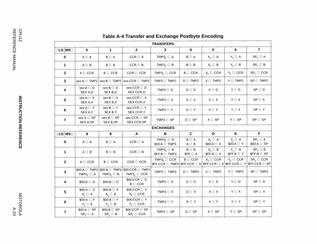
CP
U12
INS
TR
UC
TIO
N R
EF
ER
EN
CE
MO
TO
RO
LA
RE
FE
RE
NC
E M
AN
UA
LA
-23
6 7
YL ⇒ A SPL ⇒ A
YL ⇒ B SPL ⇒ B
YL ⇒ CCR SPL ⇒ CCR
Y ⇒ TMP2 SP ⇒ TMP2
Y ⇒ D SP ⇒ D
Y ⇒ X SP ⇒ X
Y ⇒ Y SP ⇒ Y
Y ⇒ SP SP ⇒ SP
E F
YL ⇒ A$00:A ⇒ Y
SPL ⇒ A$00:A ⇒ SP
YL ⇒ B$FF:B ⇒ Y
SPL ⇒ B$FF:B ⇒ SP
XYL ⇒ CCR
$FF:CCR ⇒ YSPL ⇒ CCR
$FF:CCR ⇒ SP
Y ⇔ TMP2 SP ⇔ TMP2
Y ⇔ D SP ⇔ D
Y ⇔ X SP ⇔ X
Y ⇔ Y SP ⇔ Y
Y ⇔ SP SP ⇔ SP
Table A-4 Transfer and Exchange Postbyte Encoding
TRANSFERS
⇓ LS MS⇒ 0 1 2 3 4 5
0 A ⇒ A B ⇒ A CCR ⇒ A TMP3L ⇒ A B ⇒ A XL ⇒ A
1 A ⇒ B B ⇒ B CCR ⇒ B TMP3L ⇒ B B ⇒ B XL ⇒ B
2 A ⇒ CCR B ⇒ CCR CCR ⇒ CCR TMP3L ⇒ CCR B ⇒ CCR XL ⇒ CCR
3 sex:A ⇒ TMP2 sex:B ⇒ TMP2 sex:CCR ⇒ TMP2 TMP3 ⇒ TMP2 D ⇒ TMP2 X ⇒ TMP2
4sex:A ⇒ DSEX A,D
sex:B ⇒ DSEX B,D
sex:CCR ⇒ DSEX CCR,D
TMP3 ⇒ D D ⇒ D X ⇒ D
5sex:A ⇒ XSEX A,X
sex:B ⇒ XSEX B,X
sex:CCR ⇒ XSEX CCR,X
TMP3 ⇒ X D ⇒ X X ⇒ X
6sex:A ⇒ YSEX A,Y
sex:B ⇒ YSEX B,Y
sex:CCR ⇒ YSEX CCR,Y
TMP3 ⇒ Y D ⇒ Y X ⇒ Y
7sex:A ⇒ SPSEX A,SP
sex:B ⇒ SPSEX B,SP
sex:CCR ⇒ SPSEX CCR,SP
TMP3 ⇒ SP D ⇒ SP X ⇒ SP
EXCHANGES
⇓ LS MS⇒ 8 9 A B C D
0 A ⇔ A B ⇔ A CCR ⇔ ATMP3L ⇒ A
$00:A ⇒ TMP3B ⇒ AA ⇒ B
XL ⇒ A$00:A ⇒ X
1 A ⇔ B B ⇔ B CCR ⇔ BTMP3L ⇒ B
$FF:B ⇒ TMP3B ⇒ B
$FF ⇒ AXL ⇒ B
$FF:B ⇒ X
2 A ⇔ CCR B ⇔ CCR CCR ⇔ CCRTMP3L ⇒ CCR
$FF:CCR ⇒ TMP3B ⇒ CCR
$FF:CCR ⇒ DXL ⇒ CCR
$FF:CCR ⇒
3$00:A ⇒ TMP2
TMP2L ⇒ A$00:B ⇒ TMP2
TMP2L ⇒ B$00:CCR ⇒ TMP2
TMP2L ⇒ CCRTMP3 ⇔ TMP2 D ⇔ TMP2 X ⇔ TMP2
4 $00:A ⇒ D $00:B ⇒ D$00:CCR ⇒ D
B ⇒ CCRTMP3 ⇔ D D ⇔ D X ⇔ D
5$00:A ⇒ X
XL ⇒ A$00:B ⇒ X
XL ⇒ B$00:CCR ⇒ X
XL ⇒ CCRTMP3 ⇔ X D ⇔ X X ⇔ X
6$00:A ⇒ Y
YL ⇒ A$00:B ⇒ Y
YL ⇒ B$00:CCR ⇒ Y
YL ⇒ CCRTMP3 ⇔ Y D ⇔ Y X ⇔ Y
7$00:A ⇒ SP
SPL ⇒ A$00:B ⇒ SP
SPL ⇒ B$00:CCR ⇒ SP
SPL ⇒ CCRTMP3 ⇔ SP D ⇔ SP X ⇔ SP

Key to Table A-3
Table A-5 Indexed Addressing Mode Summary
PostbyteCode (xb)
OperandSyntax Comments
rr0nnnnn ,rn,r–n,r
5-bit constant offsetn = –16 to +15rr can specify X, Y, SP, or PC
111rr0zs n,r–n,r
Constant offset (9- or 16-bit signed)z- 0 = 9-bit with sign in LSB of postbyte (s)
1 = 16-bitif z = s = 1, 16-bit offset indexed-indirect (see below)rr can specify X, Y, SP, or PC
111rr011 [n,r] 16-bit offset indexed-indirectrr can specify X, Y, SP, or PC
rr1pnnnn n,–rn,+rn,r–n,r+
Auto pre-decrement /increment or Auto post-decrement/increment ;p = pre-(0) or post-(1), n = –8 to –1, +1 to +8rr can specify X, Y, or SP (PC not a valid choice)
111rr1aa A,rB,rD,r
Accumulator offset (unsigned 8-bit or 16-bit)aa - 00 = A
01 = B10 = D (16-bit)11 = see accumulator D offset indexed-indirect
rr can specify X, Y, SP, or PC
111rr111 [D,r] Accumulator D offset indexed-indirectrr can specify X, Y, SP, or PC
postbyte (hex)B0#,REG
type
type offset used
source code syntax
MOTOROLA INSTRUCTION REFERENCE CPU12
A-24 REFERENCE MANUAL

Table A-6 Loop Primitive Postbyte Encoding (lb)00 ADBEQ
(+)
10 ADBEQ
(–)
20 ADBNE
(+)
30 ADBNE
(–)
40 ATBEQ
(+)
50 ATBEQ
(–)
60 ATBNE
(+)
70 ATBNE
(–)
80 AIBEQ
(+)
90 AIBEQ
(–)
A0 AIBNE
(+)
B0 AIBNE
(–)01 BDBEQ
(+)
11 BDBEQ
(–)
21 BDBNE
(+)
31 BDBNE
(–)
41 BTBEQ
(+)
51 BTBEQ
(–)
61 BTBNE
(+)
71 BTBNE
(–)
81 BIBEQ
(+)
91 BIBEQ
(–)
A1 BIBNE
(+)
B1 BIBNE
(–)02
—12
—22
—32
—42
—52
—62
—72
—82
—92
—A2
—B2
—
03—
13—
23—
33—
43—
53—
63—
73—
83—
93—
A3—
B3—
04 DDBEQ
(+)
14 DDBEQ
(–)
24 DDBNE
(+)
34 DDBNE
(–)
44 DTBEQ
(+)
54 DTBEQ
(–)
64 DTBNE
(+)
74 DTBNE
(–)
84 DIBEQ
(+)
94 DIBEQ
(–)
A4 DIBNE
(+)
B4 DIBNE
(–)05 XDBEQ
(+)
15 XDBEQ
(–)
25 XDBNE
(+)
35 XDBNE
(–)
45 XTBEQ
(+)
55 XTBEQ
(–)
65 XTBNE
(+)
75 XTBNE
(–)
85 XIBEQ
(+)
95 XIBEQ
(–)
A5 XIBNE
(+)
B5 XIBNE
(–)06 YDBEQ
(+)
16 YDBEQ
(–)
26 YDBNE
(+)
36 YDBNE
(–)
46 YTBEQ
(+)
56 YTBEQ
(–)
66 YTBNE
(+)
76 YTBNE
(–)
86 YIBEQ
(+)
96 YIBEQ
(–)
A6 YIBNE
(+)
B6 YIBNE
(–)07 SPDBEQ
(+)
17 SPDBEQ
(–)
27 SPDBNE
(+)
37 SPDBNE
(–)
47 SPTBEQ
(+)
57 SPTBEQ
(–)
67 SPTBNE
(+)
77 SPTBNE
(–)
87 SPIBEQ
(+)
97 SPIBEQ
(–)
A7 SPIBNE
(+)
B7 SPIBNE
(–)
postbyte (hex)B0 A_BEQ
(–)
counter used
sign of 9-bit relative branch offset(lower eight bits are an extension bytefollowing postbyte)
branch condition
CPU12 INSTRUCTION REFERENCE MOTOROLA
REFERENCE MANUAL A-25

MOTOROLA INSTRUCTION REFERENCE CPU12
A-26 REFERENCE MANUAL

APPENDIX BM68HC11 TO M68HC12 UPGRADE PATH
This appendix discusses similarities and differences between the CPU12 and theM68HC11 CPU. In general, the CPU12 is a proper superset of the M68HC11. Signifi-cant changes have been made to improve the efficiency and capabilities of the CPUwithout giving up compatibility and familiarity for the large community of M68HC11programmers.
B.1 CPU12 Design Goals
The primary goals of the CPU12 design were:
• ABSOLUTE source code compatibility with the M68HC11• Same programming model• Same stacking operations• Upgrade to 16-bit architecture• Eliminate extra byte/extra cycle penalty for using index register Y• Improve performance• Improve compatibility with high level languages
B.2 Source Code Compatibility
Every M68HC11 instruction mnemonic and source code statement can be as-sembled directly with a CPU12 assembler with no modifications.
The CPU12 supports all M68HC11 addressing modes and includes several new vari-ations of indexed addressing mode. CPU12 instructions affect condition code bits inthe same way as M68HC11 instructions.
CPU12 object code is similar to but not identical to M68HC11 object code. Some pri-mary objectives, such as the elimination of the penalty for using Y, could not beachieved without object code differences. While the object code has been changed,the majority of the opcodes are identical to those of the M6800, which was developedmore than 20 years earlier.
The CPU12 assembler automatically translates a few M68HC11 instruction mnemon-ics into functionally equivalent CPU12 instructions. For example, the CPU12 does nothave an increment stack pointer (INS) instruction, so the INS mnemonic is translatedto LEAS 1,S. The CPU12 does provide single-byte DEX, DEY, INX, and INY instruc-tions because the LEAX and LEAY instructions do not affect the condition codes,while the M68HC11 instructions update the Z bit according to the result of the decre-ment or increment.
Table B-1 shows M68HC11 instruction mnemonics that are automatically translatedinto equivalent CPU12 instructions. This translation is performed by the assembler sothere is no need to modify an old M68HC11 program in order to assemble it for theCPU12. In fact, the M68HC11 mnemonics can be used in new CPU12 programs.
CPU12 M68HC11 TO M68HC12 UPGRADE PATH MOTOROLA
REFERENCE MANUAL B-1

All of the translations produce the same amount of or slightly more object code thanthe original M68HC11 instructions. However, there are offsetting savings in other in-structions. Y-indexed instructions in particular assemble into one byte less objectcode than the same M68HC11 instruction.
The CPU12 has a two-page opcode map, rather than the four-page M68HC11 map.This is largely due to redesign of the indexed addressing modes. Most of pages 2, 3,and 4 of the M68HC11 opcode map are required because Y-indexed instructions usedifferent opcodes than X-indexed instructions. Approximately two-thirds of theM68HC11 page 1 opcodes are unchanged in CPU12, and some M68HC11 opcodeshave been moved to page 1 of the CPU12 opcode map. Object code for each of themoved instructions is one byte smaller than object code for the equivalent M68HC11instruction. Table B-2 shows instructions that assemble to one byte less object codeon the CPU12.
Instruction set changes offset each other to a certain extent. Programming style alsoaffects the rate at which instructions appear. As a test, the BUFFALO monitor, an 8-Kbyte M68HC11 assembly code program, was reassembled for the CPU12. The re-sulting object code is six bytes smaller than the M68HC11 code. It is fair to concludethat M68HC11 code can be reassembled with very little change in size.
Table B-1 Translated M68HC11 Mnemonics
M68HC11Mnemonic
EquivalentCPU12 Instruction
Comments
ABXABY
LEAX B,XLEAY B,Y
Since CPU12 has accumulator offset indexing, ABX and ABY arerarely used in new CPU12 programs. ABX was one byte on M68HC11but ABY was two bytes. The LEA substitutes are two bytes.
CLCCLICLVSECSEISEV
ANDCC #$FEANDCC #$EFANDCC #$FDORCC #$01ORCC #$10ORCC #$02
ANDCC and ORCC now allow more control over the CCR, includingthe ability to set or clear multiple bits in a single instruction. Theseinstructions took one byte each on M68HC11 while the ANDCC andORCC equivalents take two bytes each.
DESINS
LEAS –1,SLEAS 1,S
Unlike DEX and INX, DES and INS did not affect CCR bits in theM68HC11, so the LEAS equivalents in CPU12 duplicate the function ofDES and INS. These instructions were one byte on M68HC11 and twobytes on CPU12.
TAPTPATSXTSYTXSTYS
XGDXXGDY
TFR A,CCRTFR CCR,A
TFR S,XTFR S,YTFR X,STFR Y,SEXG D,XEXG D,Y
The M68HC11 had a small collection of specific transfer and exchangeinstructions. CPU12 expanded this to allow transfer or exchangebetween any two CPU registers. For all but TSY and TYS (which taketwo bytes on either CPU), the CPU12 transfer/exchange costs oneextra byte compared to the M68HC11. The substitute instructions exe-cute in one cycle rather than two.
MOTOROLA M68HC11 TO M68HC12 UPGRADE PATH CPU12
B-2 REFERENCE MANUAL

The relative size of code for M68HC11 vs. code for CPU12 has also been tested byrewriting several smaller programs from scratch. In these cases, the CPU12 code istypically about 30% smaller. These savings are mostly due to improved indexed ad-dressing.
It seems useful to mention the results of size comparisons done on C programs. A Cprogram compiled for the CPU12 is about 30% smaller than the same program com-piled for the M68HC11. The savings are largely due to better indexing.
B.3 Programmer’s Model and Stacking
The CPU12 programming model and stacking order are identical to those of theM68HC11.
B.4 True 16-Bit Architecture
The M68HC11 is a direct descendant of the M6800, one of the first microprocessors,which was introduced in 1974. The M6800 was strictly an 8-bit machine, with 8-bitdata buses and 8-bit instructions. As Motorola devices evolved from the M6800 to theM68HC11, a number of 16-bit instructions were added, but the data buses remainedeight bits wide, so these instructions were performed as sequences of 8-bit opera-tions. The CPU12 is a true 16-bit implementation, but it retains the ability to work withthe mostly 8-bit M68HC11 instruction set. The larger ALU of the CPU12 (it can per-form some 20-bit operations) is used to calculate 16-bit pointers and to speed upmath operations.
Table B-2 Instructions with Smaller Object Code
Instruction Comments
DEYINY
Page 2 opcodes in M68HC11 but page 1 in CPU12.
INST n,Y
For values of n less than 16 (the majority of cases). Were on page 2, now are on page 1.Applies to BSET, BCLR, BRSET, BRCLR, NEG, COM, LSR, ROR, ASR, ASL, ROL,DEC, INC, TST, JMP, CLR, SUB, CMP, SBC, SUBD, ADDD, AND, BIT, LDA, STA, EOR,ADC, ORA, ADD, JSR, LDS, and STS. If X is the index reference and the offset is greaterthan 15 (much less frequent than offsets of 0, 1, and 2), the CPU12 instruction assemblesto one byte more of object code than the equivalent M68HC11 instruction.
PSHYPULY
Were on page 2, now are on page 1.
LDYSTYCPY
Were on page 2, now are on page 1.
CPY n,YLDY n,YSTY n,Y
For values of n less than 16 (the majority of cases). Were on page 3, now are on page 1.
CPDWas on page 2, 3, or 4, now on page 1. In the case of indexed with offset greater than 15,CPU12 and M68HC11 object code are the same size.
CPU12 M68HC11 TO M68HC12 UPGRADE PATH MOTOROLA
REFERENCE MANUAL B-3

B.4.1 Bus Structures
The CPU12 is a 16-bit processor with 16-bit data paths. Typical M68HC12 deviceshave internal and external 16-bit data paths, but some derivatives incorporate operat-ing modes that allow for an 8-bit data bus, so that a system can be built with low-cost8-bit program memory. M68HC12 MCUs include an on-chip integration module thatmanages the external bus interface. When the CPU makes a 16-bit access to a re-source that is served by an 8-bit bus, the integration module performs two 8-bit ac-cesses, freezes the CPU clocks for part of the sequence, and assembles the data intoa 16-bit word. As far as the CPU is concerned, there is no difference between this ac-cess and a 16-bit access to an internal resource via the 16-bit data bus. This is simi-lar to the way an M68HC11 can stretch clock cycles to accommodate slowperipherals.
B.4.2 Instruction Queue
The CPU12 has a two-word instruction queue and a 16-bit holding buffer, whichsometimes acts as a third word for queueing program information. All program infor-mation is fetched from memory as aligned 16-bit words, even though there is no re-quirement for instructions to begin or end on even word boundaries. There is nopenalty for misaligned instructions. If a program begins on an odd boundary (if the re-set vector is an odd address), program information is fetched to fill the instructionqueue, beginning with the aligned word at the next address below the misaligned re-set vector. The instruction queue logic starts execution with the opcode in the low or-der half of this word.
The instruction queue causes three bytes of program information (starting with the in-struction opcode) to be directly available to the CPU at the beginning of every instruc-tion. As it executes, each instruction performs enough additional program fetches torefill the space it took up in the queue. Alignment information is maintained by the log-ic in the instruction queue. The CPU provides signals that tell the queue logic when toadvance a word of program information, and when to toggle the alignment status.
The CPU is not aware of instruction alignment. The queue logic includes a multiplexerthat sorts out the information in the queue to present the opcode and the next twobytes of information as CPU inputs. The multiplexer determines whether the opcodeis in the even or odd half of the word at the head of the queue. Alignment status isalso available to the ALU for address calculations. The execution sequence for all in-structions is independent of the alignment of the instruction.
The only situation where alignment can affect the number of cycles an instructiontakes occurs in devices that have a narrow (8-bit) external data bus, and is related tooptional program fetch cycles (O type cycles). O cycles are always performed, butserve different purposes determined by instruction size and alignment.
Each instruction includes one program fetch cycle for every two bytes of object code.Instructions with an odd number of bytes can use an O cycle to fetch an extra word ofobject code. If the queue is aligned at the start of an instruction with an odd bytecount, the last byte of object code shares a queue word with the opcode of the nextinstruction. Since this word holds part of the next instruction, the queue cannot ad-
MOTOROLA M68HC11 TO M68HC12 UPGRADE PATH CPU12
B-4 REFERENCE MANUAL

vance after the odd byte executes, or the first byte of the next instruction would belost. In this case, the O cycle appears as a free cycle since the queue is not ready toaccept the next word of program information. If this same instruction had been mis-aligned, the queue would be ready to advance and the O cycle would be used to per-form a program word fetch.
In a single-chip system or in a system with the program in 16-bit memory, both thefree cycle and the program fetch cycle take one bus cycle. In a system with the pro-gram in an external 8-bit memory, the O cycle takes one bus cycle when it appears asa free cycle, but it takes two bus cycles when used to perform a program fetch. In thiscase, the on-chip integration module freezes the CPU clocks long enough to performthe cycle as two smaller accesses. The CPU handles only 16-bit data, and is notaware that the 16-bit program access is split into two 8-bit accesses.
In order to allow development systems to track events in the CPU12 instructionqueue, two status signals (IPIPE[1:0]) provide information about data movement inthe queue and about the start of instruction execution. A development system canuse this information along with address and data information to externally reconstructthe queue. This representation of the queue can also track both the data and addressbuses.
B.4.3 Stack Function
Both the M68HC11 and the CPU12 stack nine bytes for interrupts. Since this is anodd number of bytes, there is no practical way to assure that the stack will stayaligned. To assure that instructions take a fixed number of cycles regardless of stackalignment, the internal RAM in M68HC12 MCUs is designed to allow single cycle 16-bit accesses to misaligned addresses. As long as the stack is located in this specialRAM, stacking and unstacking operations take the same amount of execution time,regardless of stack alignment. If the stack is located in an external 16-bit RAM, aPSHX instruction can take two or three cycles depending upon the alignment of thestack. This extra access time is transparent to the CPU because the integration mod-ule freezes the CPU clocks while it performs the extra 8-bit bus cycle required for amisaligned stack operation.
The CPU12 has a “last-used” stack rather than a “next-available” stack like theM68HC11 CPU. That is, the stack pointer points to the last 16-bit stack address used,rather than to the address of the next available stack location. This generally has verylittle effect, because it is very unusual to access stacked information using absoluteaddressing. The change allows a 16-bit word of data to be removed from the stackwithout changing the value of the SP twice.
To illustrate, consider the operation of a PULX instruction. With the next-availableM68HC11 stack, if the SP = $01F0 when execution begins, the sequence of opera-tions is: SP = SP + 1; load X from $01F1:01F2; SP = SP + 1; and the SP ends up at$01F2. With the last-used CPU12 stack, if the SP = $01F0 when execution begins,the sequence is: load X from $01F0:01F1; SP = SP + 2; and the SP again ends up at$01F2. The second sequence requires one less stack pointer adjustment.
CPU12 M68HC11 TO M68HC12 UPGRADE PATH MOTOROLA
REFERENCE MANUAL B-5

The stack pointer change also affects operation of the TSX and TXS instructions. Inthe M68HC11, TSX increments the SP by one during the transfer. This adjustmentcauses the X index to point to the last stack location used. The TXS instruction oper-ates similarly, except that it decrements the SP by one during the transfer. CPU12TSX and TXS instructions are ordinary transfers — the CPU12 stack requires no ad-justment.
For ordinary use of the stack, such as pushes, pulls, and even manipulations involv-ing TSX and TXS, there are no differences in the way the M68HC11 and the CPU12stacks look to a programmer. However, the stack change can affect a program algo-rithm in two subtle ways.
The LDS #$xxxx instruction is normally used to initialize the stack pointer at the startof a program. In the M68HC11, the address specified in the LDS instruction is the firststack location used. In the CPU12, however, the first stack location used is one ad-dress lower than the address specified in the LDS instruction. Since the stack buildsdownward, M68HC11 programs reassembled for the CPU12 operate normally, butthe program stack is one physical address lower in memory.
In very uncommon situations, such as test programs used to verify CPU operation, aprogram could initialize the SP, stack data, and then read the stack via an extendedmode read (it is normally improper to read stack data from an absolute extended ad-dress). To make an M68HC11 source program that contains such a sequence workon the CPU12, change either the initial LDS #$xxxx, or the absolute extended ad-dress used to read the stack.
B.5 Improved Indexing
The CPU12 has significantly improved indexed addressing capability, yet retainscompatibility with the M68HC11. The one cycle and one byte cost of doing Y-relatedindexing in the M68HC11 has been eliminated. In addition, high level language re-quirements, including stack relative indexing and the ability to perform pointer arith-metic directly in the index registers, have been accommodated.
The M68HC11 has one variation of indexed addressing that works from X or Y as thereference pointer. For X indexed addressing, an 8-bit unsigned offset in the instruc-tion is added to the index pointer to arrive at the address of the operand for the in-struction. A load accumulator instruction assembles into two bytes of object code, theopcode and a 1-byte offset. Using Y as the reference, the same instruction assem-bles into three bytes (a page prebyte, the opcode, and a one-byte offset.) Analysis ofM68HC11 source code indicates that the offset is most frequently zero and very sel-dom greater than four.
The CPU12 indexed addressing scheme uses a postbyte plus 0, 1, or 2 extensionbytes after the instruction opcode. These bytes specify which index register is used,determine whether an accumulator is used as the offset, implement automatic pre/post increment/decrement of indices, and allow a choice of 5-, 9-, or 16-bit signed off-sets. This approach eliminates the differences between X and Y register use and dra-matically enhances indexed addressing capabilities.
MOTOROLA M68HC11 TO M68HC12 UPGRADE PATH CPU12
B-6 REFERENCE MANUAL

Major improvements that result from this new approach are:
• Stack pointer can be used as an index register in all indexed operations• Program counter can be used as index register in all but auto inc/dec modes• Accumulator offsets allowed using A, B, or D accumulators• Automatic pre- or post-, increment or decrement (by –8 to +8)• 5-bit, 9-bit, or 16-bit signed constant offsets• 16-bit offset indexed-indirect and accumulator D offset indexed-indirect
The change completely eliminates pages three and four of the M68HC11 opcodemap and eliminates almost all instructions from page two of the opcode map. For off-sets of +0 to +15 from the X index register, the object code is the same size as it wasfor the M68HC11. For offsets of +0 to +15 from the Y index register, the object code isone byte smaller than it was for the M68HC11.
Table A-5 summarizes M68HC12 indexed addressing mode capabilities. Table A-3shows how the postbyte is encoded.
B.5.1 Constant Offset Indexing
The CPU12 offers three variations of constant offset indexing in order to optimize theefficiency of object code generation.
The most common constant offset is zero. Offsets of 1, 2,…4 are used fairly often, butwith less frequency than zero.
The 5-bit constant offset variation covers the most frequent indexing requirements byincluding the offset in the postbyte. This reduces a load accumulator indexed instruc-tion to two bytes of object code, and matches the object code size of the smallestM68HC11 indexed instructions, which can only use X as the index register. TheCPU12 can use X, Y, SP, or PC as the index reference with no additional object codesize cost.
The signed 9-bit constant offset indexing mode covers the same positive range as theM68HC11 8-bit unsigned offset. The size was increased to nine bits with the sign bit(ninth bit) included in the postbyte, and the remaining 8-bits of the offset in a singleextension byte.
The 16-bit constant offset indexing mode allows indexed access to the entire normal64-Kbyte address space. Since the address consists of 16 bits, the 16-bit offset canbe regarded as a signed (–32,768 to +32767) or unsigned (0 to 65,535) value. In 16-bit constant offset mode, the offset is supplied in two extension bytes after the opcodeand postbyte.
CPU12 M68HC11 TO M68HC12 UPGRADE PATH MOTOROLA
REFERENCE MANUAL B-7

B.5.2 Auto-Increment Indexing
The CPU12 provides greatly enhanced auto increment and decrement modes of in-dexed addressing. In the CPU12, the index modification may be specified for beforethe index is used (pre-), or after the index is used (post-), and the index can be incre-mented or decremented by any amount from one to eight, independent of the size ofthe operand that was accessed. X, Y, and SP can be used as the index reference, butthis mode does not allow PC to be the index reference (this would interfere with prop-er program execution).
This addressing mode can be used to implement a software stack structure, or to ma-nipulate data structures in lists or tables, rather than manipulating bytes or words ofdata. Anywhere an M68HC11 program has an increment or decrement index registeroperation near an indexed mode instruction, the increment or decrement operationcan be combined with the indexed instruction with no cost in object code size, asshown in the following code comparison.
The M68HC11 object code requires seven bytes, while the CPU12 requires only twobytes to accomplish the same functions. Three bytes of M68HC11 code were due tothe page prebyte for each Y-related instruction ($18). CPU12 post-increment indexingcapability allowed the two INY instructions to be absorbed into the LDAA indexedinstruction. The replacement code is not identical to the original three instruction se-quence because the Z condition code bit is affected by the M68HC11 INY instruc-tions, while the Z bit in the CPU12 would be determined by the value loaded into A.
B.5.3 Accumulator Offset Indexing
This indexed addressing variation allows the programmer to use either an 8-bit accu-mulator (A or B), or the 16-bit D accumulator as the offset for indexed addressing.This allows for a program-generated offset, which is more difficult to achieve in theM68HC11. The following code compares the M68HC11 and CPU12 operations.
The CPU12 object code is only one byte smaller, but the LDX # instruction is outsidethe loop. It is not necessary to reload the base address in the index register on eachpass through the loop because the LDAA B,X instruction does not alter the indexregister. This reduces the loop execution time from 15 cycles to six cycles. This re-duction, combined with the 8-MHz bus speed of the M68HC12 family, can have signif-icant effects.
18 A6 0018 0818 08
LDAA 0,YINYINY
A6 71 LDAA 2,Y+
C6 05CE 10 003AA6 00
5A26 F7
LDAB #$5 [2]LOOP LDX #$1000 [3]
ABX [3]LDAA 0,X [4]|DECB [2]BNE LOOP [3]
C6 05CE 10 00A6 E5
04 31 FB
LDAB #$5 [1]LDX #$1000 [2]
LOOP LDAA B,X [3]|DBNE B,LOOP [3]
MOTOROLA M68HC11 TO M68HC12 UPGRADE PATH CPU12
B-8 REFERENCE MANUAL

B.5.4 Indirect Indexing
The CPU12 allows some forms of indexed indirect addressing where the instructionpoints to a location in memory where the address of the operand is stored. This is anextra level of indirection compared to ordinary indexed addressing. The two forms ofindexed indirect addressing are 16-bit constant offset indexed indirect and D accumu-lator indexed indirect. The reference index register can be X, Y, SP, or PC as in otherCPU12 indexed addressing modes. PC-relative indirect addressing is one of the morecommon uses of indexed indirect addressing. The indirect variations of indexed ad-dressing help in the implementation of pointers. D accumulator indexed indirect ad-dressing can be used to implement a runtime computed GOTO function. Indirectaddressing is also useful in high level language compilers. For instance, PC-relativeindirect indexing can be used to efficiently implement some C case statements.
B.6 Improved Performance
The CPU12 improves on M68HC11 performance in several ways. M68HC12 devicesare designed using sub-micron design rules, and fabricated using advanced semi-conductor processing, the same methods used to manufacture the M68HC16 andM68300 families of modular microcontrollers. M68HC12 devices have a base busspeed of eight MHz, and are designed to operate over a wide range of supply voltag-es. The 16-bit wide architecture also increases performance. Beyond these obviousimprovements, the CPU12 uses a reduced number of cycles for many of its instruc-tions, and a 20-bit ALU makes certain CPU12 math operations much faster.
B.6.1 Reduced Cycle Counts
No M68HC11 instruction takes less than two cycles, but the CPU12 has more than 50opcodes that take only one cycle. Some of the reduction comes from the instructionqueue, which assures that several program bytes are available at the start of each in-struction. Other cycle reductions occur because the CPU12 can fetch 16 bits of infor-mation at a time, rather than eight bits at a time.
B.6.2 Fast Math
The CPU12 has some of the fastest math ever designed into a Motorola general-pur-pose MCU. Much of the speed is due to a 20-bit ALU that can perform two smaller op-erations simultaneously. The ALU can also perform two operations in a single buscycle in certain cases. Table B-3 compares the speed of CPU12 and M68HC11 mathinstructions. The CPU12 requires fewer cycles to perform an operation, and the cycletime is half that of the M68HC11.
CPU12 M68HC11 TO M68HC12 UPGRADE PATH MOTOROLA
REFERENCE MANUAL B-9

The IDIVS instruction is included specifically for C compilers, where word-sized oper-ands are divided to produce a word-sized result (unlike the 32 ÷ 16 = 16 EDIV). TheEMUL and EMULS instructions place the result in registers so a C compiler canchoose to use only 16 bits of the 32-bit result.
B.6.3 Code Size Reduction
CPU12 assembly language programs written from scratch tend to be 30% smallerthan equivalent programs written for the M68HC11. This figure has been indepen-dently qualified by Motorola programmers and an independent C compiler vendor.The major contributors to the reduction appear to be improved indexed addressingand the universal transfer/exchange instruction.
In some specialized areas, the reduction is much greater. A fuzzy logic inference ker-nel requires about 250 bytes in the M68HC11, and the same program for the CPU12requires about 50 bytes. The CPU12 fuzzy logic instructions replace whole subrou-tines in the M68HC11 version. Table lookup instructions also greatly reduce codespace.
Other CPU12 code space reductions are more subtle. Memory to memory moves areone example. The CPU12 move instruction requires almost as many bytes as anequivalent sequence of M68HC11 instructions, but the move operations themselvesdo not require the use of an accumulator. This means that the accumulator oftenneed not be saved and restored, which saves instructions.
Table B-3 Comparison of Math Instruction Speeds
InstructionMnemonic
MathOperation
M68HC111 Cycle = 250
ns
M68HC11w/Coprocessor1 Cycle = 250 ns
CPU121 Cycle = 125 ns
MUL8 × 8 = 16(signed)
10 cycles — 3 cycles
EMUL16 × 16 = 32(unsigned)
— 20 cycles 3 cycles
EMULS16 × 16 = 32
(signed)— 20 cycles 3 cycles
IDIV16 ÷ 16 = 16(unsigned)
41 cycles — 12 cycles
FDIV16 ÷ 16 = 16(fractional)
41 cycles — 12 cycles
EDIV32 ÷ 16 = 16(unsigned)
— 33 cycles 11 cycles
EDIVS32 ÷ 16 = 16
(signed)— 37 cycles 12 cycles
IDIVS16 ÷ 16 = 16
(signed)— — 12 cycles
EMACS32 × (16 × 16) ⇒ 32
(signed MAC)— 20 cycles 12 cycles
MOTOROLA M68HC11 TO M68HC12 UPGRADE PATH CPU12
B-10 REFERENCE MANUAL

Arithmetic on index pointers is another example. The M68HC11 usually requires thatthe content of the index register be moved into accumulator D, where calculations areperformed, then back to the index register before indexing can take place. In theCPU12, the LEAS, LEAX, and LEAY instructions perform arithmetic operations direct-ly on the index pointers. The pre-/post-increment/decrement variations of indexed ad-dressing also allow index modification to be incorporated into an existing indexedinstruction rather than performing the index modification as a separate operation.
Transfer and exchange operations often allow register contents to be temporarilysaved in another register rather than having to save the contents in memory. SomeCPU12 instructions such as MIN and MAX combine the actions of several M68HC11instructions into a single operation.
B.7 Additional Functions
The CPU12 incorporates a number of new instructions that provide added functional-ity and code efficiency. Among other capabilities, these new instructions allow effi-cient processing for fuzzy logic applications and support subroutine processing inextended memory beyond the standard 64-Kbyte address map for M68HC12 devicesincorporating this feature. Table B-4 is a summary of these new instructions. Subse-quent paragraphs discuss significant enhancements.
Table B-4 New M68HC12 Instructions
Mnemonic Addressing Modes Brief Functional DescriptionANDCC Immediate AND CCR with Mask (replaces CLC, CLI, and CLV)BCLR Extended Bit(s) Clear (added extended mode)BGND Inherent Enter Background Debug Mode, if enabledBRCLR Extended Branch if Bit(s) Clear (added extended mode)BRSET Extended Branch if Bit(s) Set (added extended mode)BSET Extended Bit(s) Set (added extended mode)
CALL Extended, IndexedSimilar to JSR Except also Stacks PPAGE ValueWith RTC instruction, allows easy access to >64-Kbyte space
CPS Immediate, Direct,Extended, and Indexed Compare Stack Pointer
DBNE Relative Decrement and Branch if Equal to Zero (Looping Primitive)DBEQ Relative Decrement and Branch if Not Equal to Zero (Looping Primitive)EDIV Inherent Extended Divide Y:D/X = Y(Q) and D(R) (Unsigned)
EDIVS Inherent Extended Divide Y:D/X = Y(Q) and D(R) (Signed)EMACS Special Multiply and Accumulate 16 × 16 ⇒ 32 (Signed)EMAXD Indexed Maximum of Two Unsigned 16-Bit ValuesEMAXM Indexed Maximum of Two Unsigned 16-Bit ValuesEMIND Indexed Minimum of Two Unsigned 16-Bit ValuesEMINM Indexed Minimum of Two Unsigned 16-Bit ValuesEMUL Special Extended Multiply 16 × 16 ⇒ 32; M(idx) ∗ D ⇒ Y:D
EMULS Special Extended Multiply 16 × 16 ⇒ 32 (signed); M(idx) ∗ D ⇒ Y:DETBL Special Table Lookup and Interpolate (16-bit entries)EXG Inherent Exchange Register ContentsIBEQ Relative Increment and Branch if Equal to Zero (Looping Primitive)IBNE Relative Increment and Branch if Not Equal to Zero (Looping Primitive)IDIVS Inherent Signed Integer Divide D/X ⇒ X(Q) and D(R) (Signed)
CPU12 M68HC11 TO M68HC12 UPGRADE PATH MOTOROLA
REFERENCE MANUAL B-11

LBCC Relative Long Branch if Carry Clear (Same as LBHS)LBCS Relative Long Branch if Carry Set (Same as LBLO)LBEQ Relative Long Branch if Equal (Z=1)LBGE Relative Long Branch if Greater than or Equal to ZeroLBGT Relative Long Branch if Greater than ZeroLBHI Relative Long Branch if HigherLBHS Relative Long Branch if Higher or Same (Same as LBCC)LBLE Relative Long Branch if Less than or Equal to ZeroLBLO Relative Long Branch if Lower (Same as LBCS)LBLS Relative Long Branch if Lower or SameLBLT Relative Long Branch if Less than ZeroLBMI Relative Long Branch if MinusLBNE Relative Long Branch if Not Equal to ZeroLBPL Relative Long Branch if PlusLBRA Relative Long Branch AlwaysLBRN Relative Long Branch NeverLBVC Relative Long Branch if Overflow ClearLBVS Relative Long Branch if Overflow SetLEAS Indexed Load Stack Pointer with Effective AddressLEAX Indexed Load X Index Register with Effective AddressLEAY Indexed Load Y Index Register with Effective AddressMAXA Indexed Maximum of Two Unsigned 8-Bit ValuesMAXM Indexed Maximum of Two Unsigned 8-Bit ValuesMEM Special Determine Grade of Fuzzy MembershipMINA Indexed Minimum of Two Unsigned 8-Bit ValuesMINM Indexed Minimum of Two Unsigned 8-Bit Values
MOVB(W)Combinations of
Immediate, Extended,and Indexed
Move Data from One Memory Location to Another
ORCC Immediate OR CCR with Mask (replaces SEC, SEI, and SEV)PSHC Inherent Push CCR onto StackPSHD Inherent Push Double Accumulator onto StackPULC Inherent Pull CCR Contents from StackPULD Inherent Pull Double Accumulator from StackREV Special Fuzzy Logic Rule Evaluation
REVW Special Fuzzy Logic Rule Evaluation with Weights
RTC InherentRestore Program Page and Return Address from StackUsed with CALL Instruction, Allows Easy Access to >64-Kbyte Space
SEX Inherent Sign Extend 8-bit Register into 16-bit RegisterTBEQ Relative Test and Branch if Equal to Zero (Looping Primitive)TBL Inherent Table Lookup and Interpolate (8-bit Entries)
TBNE Relative Test Register and Branch if Not Equal to Zero (Looping Primitive)TFR Inherent Transfer Register Contents to Another RegisterWAV Special Weighted Average (Fuzzy Logic Support)
Table B-4 New M68HC12 Instructions (Continued)
Mnemonic Addressing Modes Brief Functional Description
MOTOROLA M68HC11 TO M68HC12 UPGRADE PATH CPU12
B-12 REFERENCE MANUAL

B.7.1 Memory-to-Memory Moves
The CPU12 has both 8- and 16-bit variations of memory-to-memory move instruc-tions. The source address can be specified with immediate, extended, or indexed ad-dressing modes. The destination address can be specified by extended or indexedaddressing mode. The indexed addressing mode for move instructions is limited tomodes that require no extension bytes (9- and 16-bit constant offsets are not al-lowed), and indirect indexing is not allowed for moves. This leaves a 5-bit signed con-stant offset, accumulator offsets, and the automatic increment/decrement modes.The following simple loop is a block move routine capable of moving up to 256 wordsof information from one memory area to another.
LOOP MOVW 2,X+ , 2,Y+ ;move a word and update pointersDBNE B,LOOP ;repeat B times
The move immediate to extended is a convenient way to initialize a register withoutusing an accumulator or affecting condition codes.
B.7.2 Universal Transfer and Exchange
The M68HC11 has only eight transfer instructions and two exchange instructions.The CPU12 has a universal transfer/exchange instruction that can be used to transferor exchange data between any two CPU registers. The operation is obvious when thetwo registers are the same size, but some of the other combinations provide veryuseful results. For example when an 8-bit register is transferred to a 16-bit register, asign-extend operation is performed. Other combinations can be used to perform azero-extend operation.
These instructions are used often in CPU12 assembly language programs. Transferscan be used to make extra copies of data in another register, and exchanges can beused to temporarily save data during a call to a routine that expects data in a specificregister. This is sometimes faster and produces more compact object code than sav-ing data to memory with pushes or stores.
B.7.3 Loop Construct
The CPU12 instruction set includes a new family of six loop primitive instructions.These instructions decrement, increment, or test a loop count in a CPU register andthen branch based on a zero or non-zero test result. The CPU registers that can beused for the loop count are A, B, D, X, Y, or SP. The branch range is a 9-bit signed val-ue (–512 to +511) which gives these instructions twice the range of a short branch in-struction.
B.7.4 Long Branches
All of the branch instructions from the M68HC11 are also available with 16-bit offsetswhich allows them to reach any location in the 64-Kbyte address space.
CPU12 M68HC11 TO M68HC12 UPGRADE PATH MOTOROLA
REFERENCE MANUAL B-13

B.7.5 Minimum and Maximum Instructions
Control programs often need to restrict data values within upper and lower limits. TheCPU12 facilitates this function with 8- and 16-bit versions of MIN and MAX instruc-tions. Each of these instructions has a version that stores the result in either the accu-mulator or in memory.
For example, in a fuzzy logic inference program, rule evaluation consists of a series ofMIN and MAX operations. The min operation is used to determine the smallest ruleinput (the running result is held in an accumulator), and the max operation is used tostore the largest rule truth value (in an accumulator) or the previous fuzzy output val-ue (in a RAM location), to the fuzzy output in RAM. The following code demonstrateshow MIN and MAX instructions can be used to evaluate a rule with four inputs andtwo outputs.
LDY #OUT1 ;Point at first outputLDX #IN1 ;Point at first input valueLDAA #$FF ;start with largest 8-bit number in AMINA 1,X+ ;A=MIN(A,IN1)MINA 1,X+ ;A=MIN(A,IN2)MINA 1,X+ ;A=MIN(A,IN3)MINA 1,X+ ;A=MIN(A,IN4) so A holds smallest inputMAXM 1,Y+ ;OUT1=MAX(A,OUT1) and A is unchangedMAXM 1,Y+ ;OUT1=MAX(A,OUT2) A still has min input
Before this sequence is executed, the fuzzy outputs must be cleared to zeros (notshown). M68HC11 MIN or MAX operations are performed by executing a comparefollowed by a conditional branch around a load or store operation.
These instructions can also be used to limit a data value prior to using it as an input toa table lookup or other routine. Suppose a table is valid for input values between $20and $7F. An arbitrary input value can be tested against these limits and be replacedby the largest legal value if it is too big, or the smallest legal value if too small usingthe following two CPU12 instructions.
HILIMIT FCB $7F ;comparison value needs to be in memLOWLIMIT FCB $20 ;so it can be referenced via indexed
MINA HILIMIT,PCR ;A=MIN(A,$7F)MAXA LOWLIMIT,PCR;A=MAX(A,$20)
;A now within the legal range $20 to $7F
The “,PCR” notation is also new for the CPU12. This notation indicates the program-mer wants an appropriate offset from the PC reference to the memory location(HILIMIT or LOWLIMIT in this example), and then to assemble this instruction into aPC-relative indexed MIN or MAX instruction.
B.7.6 Fuzzy Logic Support
The CPU12 includes four instructions (MEM, REV, REVW, and WAV) specifically de-signed to support fuzzy logic programs. These instructions have a very small impacton the size of the CPU, and even less impact on the cost of a complete MCU. At thesame time these instructions dramatically reduce the object code size and executiontime for a fuzzy logic inference program. A kernel written for the M68HC11 requiredabout 250 bytes and executed in about 750 milliseconds. The CPU12 kernel usesabout 50 bytes and executes in about 50 microseconds.
MOTOROLA M68HC11 TO M68HC12 UPGRADE PATH CPU12
B-14 REFERENCE MANUAL

B.7.7 Table Lookup and Interpolation
The CPU12 instruction set includes two instructions (TBL and ETBL) for lookup andinterpolation of compressed tables. Consecutive table values are assumed to be the xcoordinates of the endpoints of a line segment. The TBL instruction uses 8-bit tableentries (y-values) and returns an 8-bit result. The ETBL instruction uses 16-bit tableentries (y-values) and returns a 16-bit result.
An indexed addressing mode is used to identify the effective address of the data pointat the beginning of the line segment, and the data value for the end point of the linesegment is the next consecutive memory location (byte for TBL and word for ETBL).In both cases, the B accumulator represents the ratio of (the x-distance from the be-ginning of the line segment to the lookup point) to (the x-distance from the beginningof the line segment to the end of the line segment). B is treated as an 8-bit binaryfraction with radix point left of the MSB, so each line segment is effectively dividedinto 256 pieces. During execution of the TBL or ETBL instruction, the difference be-tween the end point y-value and the beginning point y-value (a signed byte for TBL ora signed word for ETBL) is multiplied by the B accumulator to get an intermediatedelta-y term. The result is the y-value of the beginning point, plus this signed interme-diate delta-y value.
B.7.8 Extended Bit Manipulation
The M68HC11 CPU only allows direct or indexed addressing. This typically causesthe programmer to dedicate an index register to point at some memory area such asthe on-chip registers. The CPU12 allows all bit manipulation instructions to work withdirect, extended or indexed addressing modes.
B.7.9 Push and Pull D and CCR
The CPU12 includes instructions to push and pull the D accumulator and the CCR. Itis interesting to note that the order in which 8-bit accumulators A and B are stackedfor interrupts is the opposite of what would be expected for the upper and lower bytesof the 16-bit D accumulator. The order used originated in the M6800, an 8-bit micro-processor developed long before anyone thought 16-bit single-chip devices would bemade. The interrupt stacking order for accumulators A and B is retained for codecompatibility.
B.7.10 Compare SP
This instruction was added to the CPU12 instruction set to improve orthogonality andhigh-level language support. One of the most important requirements for C high-levellanguage support is the ability to do arithmetic on the stack pointer for such things asallocating local variable space on the stack. The LEAS –5,SP instruction is an exam-ple of how the compiler could easily allocate five bytes on the stack for local variables.LDX 5,SP+ loads X with the value on the bottom of the stack and deallocates fivebytes from the stack in a single operation that takes only two bytes of object code.
CPU12 M68HC11 TO M68HC12 UPGRADE PATH MOTOROLA
REFERENCE MANUAL B-15

B.7.11 Support for Memory Expansion
Bank switching is a common method of expanding memory beyond the 64-Kbyte limitof a CPU with a 64-Kbyte address space, but there are some known difficulties asso-ciated with bank switching. One problem is that interrupts cannot take place duringthe bank switching operation. This increases worst case interrupt latency and re-quires extra programming space and execution time.
Some M68HC12 variants include a built-in bank switching scheme that eliminatesmany of the problems associated with external switching logic. The CPU12 includesCALL and return from call (RTC) instructions that manage the interface to the bank-switching system. These instructions are analogous to the JSR and RTS instructions,except that the bank page number is saved and restored automatically during execu-tion. Since the page change operation is part of an uninterruptable instruction, manyof the difficulties associated with bank switching are eliminated. On M68HC12 deriva-tives with expanded memory capability, bank numbers are specified by on-chip con-trol registers. Since the addresses of these control registers may not be the same inall M68HC12 derivatives, the CPU12 has a dedicated control line to the on-chip inte-gration module that indicates when a memory-expansion register is being read orwritten. This allows the CPU to access the PPAGE register without knowing the regis-ter address.
The indexed indirect versions of the CALL instruction access the address of thecalled routine and the destination page value indirectly. For other addressing modevariations of the CALL instruction, the destination page value is provided as immedi-ate data in the instruction object code. CALL and RTC execute correctly in the normal64-Kbyte address space, thus providing for portable code.
MOTOROLA M68HC11 TO M68HC12 UPGRADE PATH CPU12
B-16 REFERENCE MANUAL

APPENDIX CHIGH-LEVEL LANGUAGE SUPPORT
Many programmers are turning to high-level languages such as C as an alternative tocoding in native assembly languages. High-level language (HLL) programming canimprove productivity and produce code that is more easily maintained than assemblylanguage programs. The most serious drawback to the use of HLL in MCUs has beenthe relatively large size of programs written in HLL. Larger program ROM size require-ments translate into increased system costs.
Motorola solicited the cooperation of third-party software developers to assure that theCPU12 instruction set would meet the needs of a more efficient generation of compil-ers. Several features of the CPU12 were specifically designed to improve the efficien-cy of compiled HLL, and thus minimize cost.
This appendix identifies CPU12 instructions and addressing modes that provide im-proved support for high-level language. C language examples are provided to demon-strate how these features support efficient HLL structures and concepts. Since theCPU12 instruction set is a superset of the M68HC11 instruction set, some of the dis-cussions use the M68HC11 as a basis for comparison.
C.1 Data Types
The CPU12 supports the bit-sized data type with bit manipulation instructions whichare available in extended, direct, and indexed variations. The char data type is a sim-ple 8-bit value that is commonly used to specify variables in a small microcontrollersystem because it requires less memory space than a 16-bit integer (provided the vari-able has a range small enough to fit into eight bits). The 16-bit CPU12 can easily han-dle 16-bit integer types and the available set of conditional branches (including longbranches) allow branching based on signed or unsigned arithmetic results. Some ofthe higher math functions allow for division and multiplication involving 32-bit values,although it is somewhat less common to use such long values in a microcontroller sys-tem.
The CPU12 has special sign extension instructions to allow easy type-casting fromsmaller data types to larger ones, such as from char to integer. This sign extension isautomatically performed when an 8-bit value is transferred to a 16-bit register.
C.2 Parameters and Variables
High-level languages make extensive use of the stack, both to pass variables and fortemporary and local storage. It follows that there should be easy ways to push and pullall CPU registers, stack pointer based indexing should be allowed, and that directarithmetic manipulation of the stack pointer value should be allowed. The CPU12 in-struction set provided for all of these needs with improved indexed addressing, the ad-dition of an LEAS instruction, and the addition of push and pull instructions for the Daccumulator and the CCR.
CPU12 HIGH-LEVEL LANGUAGE SUPPORT MOTOROLA
REFERENCE MANUAL C-1

C.2.1 Register Pushes and Pulls
The M68HC11 has push and pull instructions for A, B, X, and Y, but requires separate8-bit pushes and pulls of accumulators A and B to stack or unstack the 16-bit D accu-mulator (the concatenated combination of A:B). The PSHD and PULD instructions al-low directly stacking the D accumulator in the expected 16-bit order.
Adding PSHC and PULC improved orthogonality by completing the set of stacking in-structions so that any of the CPU registers can be pushed or pulled. These instructionsare also useful for preserving the CCR value during a function call subroutine.
C.2.2 Allocating and Deallocating Stack Space
The LEAS instruction can be used to allocate or deallocate space on the stack for tem-porary variables:
LEAS –10,S ;Allocate space for 5 16-bit integers
LEAS 10,S ;Deallocate space for 5 16-bit ints
The (de)allocation can even be combined with a register push or pull as in the followingexample:
LDX 8,S+ ;Load return value and deallocate
X is loaded with the 16-bit integer value at the top of the stack, and the stack pointeris adjusted up by eight to deallocate space for eight bytes worth of temporary storage.Post-increment indexed addressing is used in this example, but all four combinationsof pre/post increment/decrement are available (offsets from –8 to +8 inclusive, from X,Y, or SP). This form of indexing can often be used to get an index (or stack pointer)adjustment for free during an indexed operation (the instruction requires no more codespace or cycles than a zero-offset indexed instruction).
C.2.3 Frame Pointer
In the C language, it is common to have a frame pointer in addition to the CPU stackpointer. The frame is an area of memory within the system stack which is used for pa-rameters and local storage of variables used within a function subroutine. The follow-ing is a description of how a frame pointer can be set up and used.
First, parameters (typically values in CPU registers) are pushed onto the system stackprior to using a JSR or CALL to get to the function subroutine. At the beginning of thecalled subroutine, the frame pointer of the calling program is pushed onto the stack.Typically, an index register, such as X, is used as the frame pointer, so a PSHX in-struction would save the frame pointer from the calling program.
Next, the called subroutine establishes a new frame pointer by executing a TFR S,X.Space is allocated for local variables by executing an LEAS –n,S, where n is the num-ber of bytes needed for local variables.
MOTOROLA HIGH-LEVEL LANGUAGE SUPPORT CPU12
C-2 REFERENCE MANUAL

Notice that parameters are at positive offsets from the frame pointer while locals areat negative offsets. In the M68HC11, the indexed addressing mode uses only positiveoffsets, so the frame pointer always points to the lowest address of any parameter orlocal. After the function subroutine finishes, calculations are required to restore thestack pointer to the mid-frame position between the locals and the parameters beforereturning to the calling program. The CPU12 only requires execution of TFR X,S todeallocate the local storage and return.
The concept of a frame pointer is supported in the CPU12 through a combination ofimproved indexed addressing, universal transfer/exchange, and the LEA instruction.These instructions work together to achieve more efficient handling of frame pointers.It is important to consider the complete instruction set as a complex system with subtleinterrelationships rather than simply examining individual instructions when trying toimprove an instruction set. Adding or removing a single instruction can have unexpect-ed consequences.
C.3 Increment and Decrement Operators
In C, the notation + + i or i – – is often used to form loop counters. Within limited con-straints, the CPU12 loop primitives can be used to speed up the loop count and branchfunction.
The CPU12 includes a set of six basic loop control instructions which decrement, in-crement, or test a loop count register, and then branch if it is either equal to zero or notequal to zero. The loop count register can be A, B, D, X, Y, or SP. A or B could be usedif the loop count fits in an 8-bit char variable; the other choices are all 16-bit registers.The relative offset for the loop branch is a 9-bit signed value, so these instructions canbe used with loops as long as 256 bytes.
In some cases, the pre- or post-increment operation can be combined with an indexedinstruction to eliminate the cost of the increment operation. This is typically done bypost-compile optimization because the indexed instruction that could absorb the incre-ment/decrement operation may not be apparent at compile time.
C.4 Higher Math Functions
In the CPU12, subtle characteristics of higher math operations such as IDIVS andEMUL are arranged so a compiler can handle inputs and outputs more efficiently.
The most apparent case is the IDIVS instruction, which divides two 16-bit signed num-bers to produce a 16-bit result. While the same function can be accomplished with theEDIVS instruction (a 32 by 16 divide), doing so is much less efficient because extrasteps are required to prepare inputs to the EDIVS, and because EDIVS uses the Y in-dex register. EDIVS uses a 32-bit signed numerator and the C compiler would typicallywant to use a 16-bit value (the size of an integer data type). The 16-bit C value wouldneed to be sign-extended into the upper 16-bits of the 32-bit EDIVS numerator beforethe divide operation.
CPU12 HIGH-LEVEL LANGUAGE SUPPORT MOTOROLA
REFERENCE MANUAL C-3

Operand size is also a potential problem in the extended multiply operations but thedifficulty can be minimized by putting the results in CPU registers. Having higher pre-cision math instructions is not necessarily a requirement for supporting high-level lan-guage because these functions can be performed as library functions. However, if anapplication requires these functions, the code is much more efficient if the MCU canuse native instructions instead of relatively large, slow routines.
C.5 Conditional If Constructs
In the CPU12 instruction set, most arithmetic and data manipulation instructions auto-matically update the condition code register, unlike other architectures that onlychange condition codes during a few specific compare instructions. The CPU12 in-cludes branch instructions that perform conditional branching based on the state of theindicators in the condition codes register. Short branches use a single byte relative off-set that allows branching to a destination within about ±128 locations from the branch.Long branches use a 16-bit relative offset that allows conditional branching to any lo-cation in the 64-Kbyte map.
C.6 Case and Switch Statements
Case and switch statements (and computed GOTOs) can use PC-relative indirect ad-dressing to determine which path to take. Depending upon the situation, cases canuse either the constant offset variation or the accumulator D offset variation of indirectindexed addressing.
C.7 Pointers
The CPU12 supports pointers by allowing direct arithmetic operations on the 16-bit in-dex registers (LEAS, LEAX, and LEAY instructions) and by allowing indexed indirectaddressing modes.
C.8 Function Calls
Bank switching is a fairly common way of adapting a CPU with a 16-bit address bus toaccommodate more than 64-Kbytes of program memory space. One of the most sig-nificant drawbacks of this technique has been the requirement to mask (disable) inter-rupts while the bank page value was being changed. Another problem is that thephysical location of the bank page register can change from one MCU derivative to an-other (or even due to a change to mapping controls by a user program). In these situ-ations, an operating system program has to keep track of the physical location of thepage register. The CPU12 addresses both of these problems with the uninterruptibleCALL and return from call (RTC) instructions.
The CALL instruction is similar to a JSR instruction, except that the programmer sup-plies a destination page value as part of the instruction. When CALL executes, the oldpage value is saved on the stack and the new page value is written to the bank pageregister. Since the CALL instruction is uninterruptible, this eliminates the need to sep-arately mask off interrupts during the context switch.
MOTOROLA HIGH-LEVEL LANGUAGE SUPPORT CPU12
C-4 REFERENCE MANUAL

The CPU12 has dedicated signal lines that allow the CPU to access the bank pageregister without having to use an address in the normal 64-Kbyte address space. Thiseliminates the need for the program to know where the page register is physically lo-cated.
The RTC instruction is similar to the RTS instruction, except that RTC uses the byteof information that was saved on the stack by the corresponding CALL instruction torestore the bank page register to its old value. Although a CALL/RTC pair can be usedto access any function subroutine regardless of the location of the called routine (onthe current bank page or a different page), it is most efficient to access some subrou-tines with JSR/RTS instructions when the called subroutine is on the current page orin an area of memory that is always visible in the 64-Kbyte map regardless of the bankpage selection.
Push and pull instructions can be used to stack some or all the CPU registers duringa function call. The CPU12 can push and pull any of the CPU registers A, B, CCR, D,X, Y, or SP.
C.9 Instruction Set Orthogonality
One very helpful aspect of the CPU12 instruction set, orthogonality, is difficult to quan-tify in terms of direct benefit to an HLL compiler. Orthogonality refers to the regularityof the instruction set. A completely orthogonal instruction set would allow any instruc-tion to operate in any addressing mode, would have identical code sizes and executiontimes for similar operations on different registers, and would include both signed andunsigned versions of all mathematical instructions. Greater regularity of the instructionmakes it possible to implement compilers more efficiently, because operation is moreconsistent, and fewer special cases must be handled.
CPU12 HIGH-LEVEL LANGUAGE SUPPORT MOTOROLA
REFERENCE MANUAL C-5

MOTOROLA HIGH-LEVEL LANGUAGE SUPPORT CPU12
C-6 REFERENCE MANUAL

APPENDIX DASSEMBLY LISTING
D.1 Assembler Test File
The following assembler test file illustrates all possible variations of the M68HC12 in-struction set and can be used as a quick reference for instruction syntax. Instructionsare in alphabetical order and include redundancy.
* 68HC12 assembly listing*
0072 immed equ $720055 dir equ $551234 ext equ $12340037 ind equ $37000e small equ $e00cc mask equ %11001100
**
d000 ORG $D000
d000 00 02 dw 2d002 02 db 2d003 00 02 dc.w 2d005 02 dc.b 2d006 02 fcb 2d007 08 ae fdb 2222d009 ds 34d02b ds.b 34d04d ds.w 34d091 rmb 34d0b3 rmw 34
d0f7 18 06 abad0f9 1a e5 abxd0fb 19 ed abyd0fd 89 72 adca #immedd0ff 89 72 adca #immedd101 89 72 adca #immedd103 89 72 adca #immedd105 89 72 adca #immedd107 a9 a0 adca 1,+spd109 a9 20 adca 1,+xd10b a9 60 adca 1,+yd10d a9 a7 adca 8,+spd10f a9 67 adca 8,+yd111 a9 c0 adca ,pcd113 a9 80 adca ,spd115 a9 00 adca ,xd117 a9 40 adca ,yd119 a9 af adca 1,-sp
CPU12 ASSEMBLY
REFERENCE MANUAL
d11b a9 2f adca 1,-xd11d a9 6f adca 1,-yd11f a9 a8 adca 8,-spd121 a9 28 adca 8,-xd123 a9 68 adca 8,-yd125 a9 9f adca -1,spd127 a9 1f adca -1,xd129 a9 5f adca -1,yd12b a9 90 adca -16,spd12d a9 10 adca -16,xd12f a9 50 adca -16,yd131 a9 f1 ef adca -17,spd134 a9 e1 ef adca -17,xd137 a9 e9 ef adca -17,yd13a a9 d2 adca -small,pcd13c a9 92 adca -small,spd13e a9 12 adca -small,xd140 a9 52 adca -small,yd142 a9 c0 adca 0,pcd144 a9 80 adca 0,spd146 a9 00 adca 0,xd148 a9 40 adca 0,yd14a a9 b0 adca 1,sp+d14c a9 30 adca 1,x+d14e a9 e2 01 88 adca ext,xd152 a9 e2 89 44 adca ext,xd156 a9 e2 33 33 adca ext,xd15a a9 e2 44 44 adca ext,xd15e a9 e2 01 88 adca ext,xd162 a9 70 adca 1,y+d164 a9 81 adca 1,spd166 a9 01 adca 1,xd168 a9 41 adca 1,yd16a a9 bf adca 1,sp-d16c a9 3f adca 1,x-d16e a9 7f adca 1,y-d170 a9 f8 7d adca 125,pcd173 a9 f0 7d adca 125,spd176 a9 e0 7d adca 125,xd179 a9 e8 7d adca 125,yd17c a9 8f adca 15,spd17e a9 0f adca 15,xd180 a9 4f adca 15,yd182 a9 f0 10 adca 16,spd185 a9 e0 10 adca 16,xd188 a9 e8 10 adca 16,yd18b a9 b7 adca 8,sp+d18d a9 37 adca 8,x+d18f a9 77 adca 8,y+
LISTING MOTOROLA
D-1

d191 a9 b8 adca 8,sp-d193 a9 38 adca 8,x-d195 a9 78 adca 8,y-d197 a9 f4 adca a,spd199 a9 e4 adca a,xd19b a9 ec adca a,yd19d a9 f5 adca b,spd19f a9 e5 adca b,xd1a1 a9 ed adca b,yd1a3 a9 f6 adca d,spd1a5 a9 e6 adca d,xd1a7 a9 ee adca d,yd1a9 99 55 adca dird1ab 99 55 adca dird1ad b9 01 88 adca extd1b0 b9 01 88 adca extd1b3 a9 f2 01 88 adca ext,spd1b7 a9 e2 01 88 adca ext,xd1bb a9 ea 01 88 adca ext,yd1bf a9 f8 37 adca ind,pcd1c2 a9 f0 37 adca ind,spd1c5 a9 e0 37 adca ind,xd1c8 a9 e8 37 adca ind,yd1cb a9 ce adca small,pcd1cd a9 8e adca small,spd1cf a9 0e adca small,xd1d1 a9 4e adca small,yd1d3 c9 72 adcb #immedd1d5 e9 a0 adcb 1,+spd1d7 e9 d2 adcb -small,pcd1d9 e9 f8 7d adcb 125,pcd1dc d9 55 adcb dird1de f9 01 88 adcb extd1e1 e9 f2 01 88 adcb ext,spd1e5 8b 72 adda #immedd1e7 ab a0 adda 1,+spd1e9 9b 55 adda dird1eb bb 01 88 adda extd1ee bb 01 88 adda extd1f1 cb 72 addb #immedd1f3 eb a0 addb 1,+spd1f5 db 55 addb dird1f7 fb 01 88 addb extd1fa c3 00 72 addd #immedd1fd e3 a0 addd 1,+spd1ff d3 55 addd dird201 f3 01 88 addd extd204 84 72 anda #immedd206 a4 a0 anda 1,+spd208 94 55 anda dird20a b4 01 88 anda extd20d c4 72 andb #immedd20f e4 a0 andb 1,+spd211 d4 55 andb dird213 f4 01 88 andb extd216 10 72 andcc #immedd218 68 a0 asl 1,+spd21a 78 00 55 asl dird21d 78 01 88 asl extd220 48 aslad221 58 aslbd222 59 asldd223 67 a0 asr 1,+spd225 77 00 55 asr dird228 77 01 88 asr extd22b 47 asra
MOTOROLA ASSEMB
D-2
d22c 57 asrbd22d 24 fe bcc *d22f 25 fe bcs *d231 27 fe beq *d233 2c fe bge *d235 2e fe bgt *d237 22 fe bhi *d239 85 72 bita #immedd23b a5 a0 bita 1,+spd23d 95 55 bita dird23f b5 01 88 bita extd242 c5 72 bitb #immedd244 e5 a0 bitb 1,+spd246 d5 55 bitb dird248 f5 01 88 bitb extd24b 2f fe ble *d24d 23 fe bls *d24f 2d fe blt *d251 2b fe bmi *d253 26 fe bne *d255 2a fe bpl *d257 20 fe bra *d259 21 fe brn *d25b 07 fe bsr *d25d 28 fe bvc *d25f 29 fe bvs *d261 0d a0 55 bclr 1,+sp $55d264 0d a0 55 bclr 1,+sp #$55d267 0d a0 55 bclr 1,+sp,#$55d26a 0d bf 55 bclr 1,sp-,#$55d26d 0d bf 55 bclr 1,sp- #$55
d270 0d 20 55 bclr 1,+x $55d273 0d 20 55 bclr 1,+x #$55d276 0d 20 55 bclr 1,+x,$55d279 0d 20 55 bclr 1,+x,#$55
d27c 4d 55 55 bclr dir $55d27f 4d 55 55 bclr dir #$55d282 4d 55 55 bclr dir,$55d285 4d 55 55 bclr dir,#$55
d288 1d 01 88 55 bclr ext $55d28c 1d 01 88 55 bclr ext #$55d290 1d 01 88 55 bclr ext,$55d294 1d 01 88 55 bclr ext,#$55
d298 0f a0 55 fc brclr 1,+sp $55 *d29c 0f a0 55 fc brclr 1,+sp #$55 *d2a0 0f a0 55 fc brclr 1,+sp,$55 *d2a4 0f a0 55 fc brclr 1,+sp,#$55 *
d2a8 4f 55 55 fc brclr dir $55 *d2ac 4f 55 55 fc brclr dir #$55 *d2b0 4f 55 55 fc brclr dir,$55 *d2b4 4f 55 55 fc brclr dir,#$55 *
d2b8 1f 01 88 55 fb brclr ext $55 *d2bd 1f 01 88 55 fb brclr ext #$55 *d2c2 1f 01 88 55 fb brclr ext,$55,*d2c7 1f 01 88 55 fb brclr ext,#$55,*
d2cc 0e a0 55 fc brset 1,+sp $55 *d2d0 0e a0 55 fc brset 1,+sp #$55 *d2d4 0e a0 55 fc brset 1,+sp,$55,*d2d8 0e a0 55 fc brset 1,+sp,#$55,*
LY LISTING CPU12
REFERENCE MANUAL

d2dc 4e 55 55 fc brset dir $55 *d2e0 4e 55 55 fc brset dir #$55 *d2e4 4e 55 55 fc brset dir,$55,*d2e8 4e 55 55 fc brset dir,#$55,*
d2ec 1e 01 88 55 fb brset ext $55 *d2f1 1e 01 88 55 fb brset ext #$55 *d2f6 1e 01 88 55 fb brset ext,$55,*d2fb 1e 01 88 55 fb brset ext,#$55,*
d300 0c a0 55 bset 1,+sp $55d303 0c a0 55 bset 1,+sp #$55d306 0c a0 55 bset 1,+sp,$55d309 0c a0 55 bset 1,+sp,#$55
d30c 4c 55 55 bset dir $55d30f 4c 55 55 bset dir #$55d312 4c 55 55 bset dir,$55d315 4c 55 55 bset dir,#$55
d318 1c 01 88 55 bset ext $55d31c 1c 01 88 55 bset ext #$55d320 1c 01 88 55 bset ext,$55d324 1c 01 88 55 bset ext,#$55
d328 4b a0 55 call 1,+sp $55d32b 4b 20 55 call 1,+x $55d32e 4b 60 55 call 1,+y $55d331 4b a7 55 call 8,+sp $55d334 4b 27 55 call 8,+x $55d337 4b 67 55 call 8,+y $55d33a 4b c0 55 call ,pc $55d33d 4b 80 55 call ,sp $55d340 4b 00 55 call ,x $55d343 4b 40 55 call ,y $55d346 4b af 55 call 1,-sp $55d349 4b 2f 55 call 1,-x $55d34c 4b 6f 55 call 1,-y $55d34f 4b a8 55 call 8,-sp $55d352 4b 28 55 call 8,-x $55d355 4b 68 55 call 8,-y $55d358 4b 9f 55 call -1,sp $55d35b 4b 1f 55 call -1,x $55d35e 4b 5f 55 call -1,y $55d361 4b 90 55 call -16,sp $55d364 4b 10 55 call -16,x $55d367 4b 50 55 call -16,y $55d36a 4b f1 ef 55 call -17,sp $55d36e 4b e1 ef 55 call -17,x $55d372 4b e9 ef 55 call -17,y $55d376 4b d2 55 call -small,pc $55d379 4b 92 55 call -small,sp $55d37c 4b 12 55 call -small,x $55d37f 4b 52 55 call -small,y $55d382 4b c0 55 call 0,pc $55d385 4b 80 55 call 0,sp $55d388 4b 00 55 call 0,x $55d38b 4b 40 55 call 0,y $55d38e 4b b0 55 call 1,sp+ $55d391 4b 30 55 call 1,x+ $55d394 4b 70 55 call 1,y+ $55d397 4b 81 55 call 1,sp $55d39a 4b 01 55 call 1,x $55d39d 4b 41 55 call 1,y $55d3a0 4b bf 55 call 1,sp- $55
CPU12 ASSEMBL
REFERENCE MANUAL
d3a3 4b 3f 55 call 1,x- $55d3a6 4b 7f 55 call 1,y- $55d3a9 4b f8 7d 55 call 125,pc $55d3ad 4b f0 7d 55 call 125,sp $55d3b1 4b e0 7d 55 call 125,x $55d3b5 4b e8 7d 55 call 125,y $55d3b9 4b 8f 55 call 15,sp $55d3bc 4b 0f 55 call 15,x $55d3bf 4b 4f 55 call 15,y $55d3c2 4b f0 10 55 call 16,sp $55d3c6 4b e0 10 55 call 16,x $55d3ca 4b e8 10 55 call 16,y $55d3ce 4b b7 55 call 8,sp+ $55d3d1 4b 37 55 call 8,x+ $55d3d4 4b 77 55 call 8,y+ $55d3d7 4b b8 55 call 8,sp- $55d3da 4b 38 55 call 8,x- $55d3dd 4b 78 55 call 8,y- $55d3e0 4b f4 55 call a,sp $55d3e3 4b e4 55 call a,x $55d3e6 4b ec 55 call a,y $55d3e9 4b f5 55 call b,sp $55d3ec 4b e5 55 call b,x $55d3ef 4b ed 55 call b,y $55d3f2 4b f6 55 call d,sp $55d3f5 4b e6 55 call d,x $55d3f8 4b ee 55 call d,y $55d3fb 4a 00 55 55 call dir $55d3ff 4a 01 88 55 call ext $55d403 4b f2 01 88 55 call ext,sp $55d408 4b e2 01 88 55 call ext,x $55d40d 4b ea 01 88 55 call ext,y $55d412 4b f8 37 55 call ind,pc $55d416 4b f0 37 55 call ind,sp $55d41a 4b e0 37 55 call ind,x $55d41e 4b e8 37 55 call ind,y $55d422 4b ce 55 call small,pc $55d425 4b 8e 55 call small,sp $55d428 4b 0e 55 call small,x $55d42b 4b 4e 55 call small,y $55
d42e 18 17 cbad430 10 fe clcd432 10 ef clid434 69 a0 clr 1,+spd436 79 00 55 clr dird439 79 01 88 clr extd43c 87 clrad43d c7 clrbd43e 10 fd clvd440 81 72 cmpa #immedd442 a1 a0 cmpa 1,+spd444 91 55 cmpa dird446 b1 01 88 cmpa ext
d449 c1 72 cmpb #immedd44b c1 72 cmpb #immedd44d e1 a0 cmpb 1,+spd44f e1 20 cmpb 1,+xd451 e1 60 cmpb 1,+yd453 e1 a7 cmpb 8,+spd455 e1 27 cmpb 8,+xd457 e1 67 cmpb 8,+yd459 e1 c0 cmpb ,pcd45b e1 80 cmpb ,spd45d e1 00 cmpb ,x
Y LISTING MOTOROLA
D-3

d45f e1 40 cmpb ,yd461 e1 af cmpb 1,-spd463 e1 2f cmpb 1,-xd465 e1 6f cmpb 1,-yd467 e1 a8 cmpb 8,-spd469 e1 28 cmpb 8,-xd46b e1 68 cmpb 8,-yd46d e1 9f cmpb -1,spd46f e1 1f cmpb -1,xd471 e1 5f cmpb -1,yd473 e1 90 cmpb -16,spd475 e1 10 cmpb -16,xd477 e1 50 cmpb -16,yd479 e1 f1 ef cmpb -17,spd47c e1 e1 ef cmpb -17,xd47f e1 e9 ef cmpb -17,yd482 e1 d2 cmpb -small,pcd484 e1 92 cmpb -small,spd486 e1 12 cmpb -small,xd488 e1 52 cmpb -small,yd48a e1 c0 cmpb 0,pcd48c e1 80 cmpb 0,spd48e e1 00 cmpb 0,xd490 e1 40 cmpb 0,yd492 e1 b0 cmpb 1,sp+d494 e1 30 cmpb 1,x+d496 e1 70 cmpb 1,y+d498 e1 81 cmpb 1,spd49a e1 01 cmpb 1,xd49c e1 41 cmpb 1,yd49e e1 bf cmpb 1,sp-d4a0 e1 3f cmpb 1,x-d4a2 e1 7f cmpb 1,y-d4a4 e1 f8 7d cmpb 125,pcd4a7 e1 f0 7d cmpb 125,spd4aa e1 e0 7d cmpb 125,xd4ad e1 e8 7d cmpb 125,yd4b0 e1 8f cmpb 15,spd4b2 e1 0f cmpb 15,xd4b4 e1 4f cmpb 15,yd4b6 e1 f0 10 cmpb 16,spd4b9 e1 e0 10 cmpb 16,xd4bc e1 e8 10 cmpb 16,yd4bf e1 b7 cmpb 8,sp+d4c1 e1 37 cmpb 8,x+d4c3 e1 77 cmpb 8,y+d4c5 e1 b8 cmpb 8,sp-d4c7 e1 38 cmpb 8,x-d4c9 e1 78 cmpb 8,y-d4cb e1 f4 cmpb a,spd4cd e1 e4 cmpb a,xd4cf e1 ec cmpb a,yd4d1 e1 f5 cmpb b,spd4d3 e1 e5 cmpb b,xd4d5 e1 ed cmpb b,yd4d7 e1 f6 cmpb d,spd4d9 e1 e6 cmpb d,xd4db e1 ee cmpb d,yd4dd d1 55 cmpb dird4df d1 55 cmpb dird4e1 f1 01 88 cmpb extd4e4 f1 01 88 cmpb extd4e7 e1 f2 01 88 cmpb ext,spd4eb e1 e2 01 88 cmpb ext,xd4ef e1 ea 01 88 cmpb ext,yd4f3 e1 f8 37 cmpb ind,pc
MOTOROLA ASSEMB
D-4
d4f6 e1 f0 37 cmpb ind,spd4f9 e1 e0 37 cmpb ind,xd4fc e1 e8 37 cmpb ind,yd4ff e1 ce cmpb small,pcd501 e1 8e cmpb small,spd503 e1 0e cmpb small,xd505 e1 4e cmpb small,yd507 61 a0 com 1,+spd509 61 20 com 1,+xd50b 61 60 com 1,+yd50d 61 a7 com 8,+spd50f 61 27 com 8,+xd511 61 67 com 8,+yd513 61 c0 com ,pcd515 61 80 com ,spd517 61 00 com ,xd519 61 40 com ,yd51b 61 af com 1,-spd51d 61 2f com 1,-xd51f 61 6f com 1,-yd521 61 a8 com 8,-spd523 61 28 com 8,-xd525 61 68 com 8,-yd527 61 9f com -1,spd529 61 1f com -1,xd52b 61 5f com -1,yd52d 61 90 com -16,spd52f 61 10 com -16,xd531 61 50 com -16,yd533 61 f1 ef com -17,spd536 61 e1 ef com -17,xd539 61 e9 ef com -17,yd53c 61 d2 com -small,pcd53e 61 92 com -small,spd540 61 12 com -small,xd542 61 52 com -small,yd544 61 c0 com 0,pcd546 61 80 com 0,spd548 61 00 com 0,xd54a 61 40 com 0,yd54c 61 b0 com 1,sp+d54e 61 30 com 1,x+d550 61 70 com 1,y+d552 61 81 com 1,spd554 61 01 com 1,xd556 61 41 com 1,yd558 61 bf com 1,sp-d55a 61 3f com 1,x-d55c 61 7f com 1,y-d55e 61 f8 7d com 125,pcd561 61 f0 7d com 125,spd564 61 e0 7d com 125,xd567 61 e8 7d com 125,yd56a 61 8f com 15,spd56c 61 0f com 15,xd56e 61 4f com 15,yd570 61 f0 10 com 16,spd573 61 e0 10 com 16,xd576 61 e8 10 com 16,yd579 61 b7 com 8,sp+d57b 61 37 com 8,x+d57d 61 77 com 8,y+d57f 61 b8 com 8,sp-d581 61 38 com 8,x-d583 61 78 com 8,y-d585 61 f4 com a,sp
LY LISTING CPU12
REFERENCE MANUAL

d587 61 e4 com a,xd589 61 ec com a,yd58b 61 f5 com b,spd58d 61 e5 com b,xd58f 61 ed com b,yd591 61 f6 com d,spd593 61 e6 com d,xd595 61 ee com d,yd597 71 00 55 com dird59a 71 01 88 com extd59d 71 01 88 com extd5a0 61 f2 01 88 com ext,spd5a4 61 e2 01 88 com ext,xd5a8 61 ea 01 88 com ext,yd5ac 61 f8 37 com ind,pcd5af 61 f0 37 com ind,spd5b2 61 e0 37 com ind,xd5b5 61 e8 37 com ind,yd5b8 61 ce com small,pcd5ba 61 8e com small,spd5bc 61 0e com small,xd5be 61 4e com small,yd5c0 41 comad5c1 51 combd5c2 8c 00 72 cpd #immedd5c5 8c 00 72 cpd #immedd5c8 ac a0 cpd 1,+spd5ca ac 20 cpd 1,+xd5cc ac 60 cpd 1,+yd5ce ac a7 cpd 8,+spd5d0 ac 27 cpd 8,+xd5d2 ac 67 cpd 8,+yd5d4 ac c0 cpd ,pcd5d6 ac 80 cpd ,spd5d8 ac 00 cpd ,xd5da ac 40 cpd ,yd5dc ac af cpd 1,-spd5de ac 2f cpd 1,-xd5e0 ac 6f cpd 1,-yd5e2 ac a8 cpd 8,-spd5e4 ac 28 cpd 8,-xd5e6 ac 68 cpd 8,-yd5e8 ac 9f cpd -1,spd5ea ac 1f cpd -1,xd5ec ac 5f cpd -1,yd5ee ac 90 cpd -16,spd5f0 ac 10 cpd -16,xd5f2 ac 50 cpd -16,yd5f4 ac f1 ef cpd -17,spd5f7 ac e1 ef cpd -17,xd5fa ac e9 ef cpd -17,yd5fd ac d2 cpd -small,pcd5ff ac 92 cpd -small,spd601 ac 12 cpd -small,xd603 ac 52 cpd -small,yd605 ac c0 cpd 0,pcd607 ac 80 cpd 0,spd609 ac 00 cpd 0,xd60b ac 40 cpd 0,yd60d ac b0 cpd 1,sp+d60f ac 30 cpd 1,x+d611 ac 70 cpd 1,y+d613 ac 81 cpd 1,spd615 ac 01 cpd 1,xd617 ac 41 cpd 1,yd619 ac bf cpd 1,sp-
CPU12 ASSEMBL
REFERENCE MANUAL
d61b ac 3f cpd 1,x-d61d ac 7f cpd 1,y-d61f ac f8 7d cpd 125,pcd622 ac f0 7d cpd 125,spd625 ac e0 7d cpd 125,xd628 ac e8 7d cpd 125,yd62b ac 8f cpd 15,spd62d ac 0f cpd 15,xd62f ac 4f cpd 15,yd631 ac f0 10 cpd 16,spd634 ac e0 10 cpd 16,xd637 ac e8 10 cpd 16,yd63a ac b7 cpd 8,sp+d63c ac 37 cpd 8,x+d63e ac 77 cpd 8,y+d640 ac b8 cpd 8,sp-d642 ac 38 cpd 8,x-d644 ac 78 cpd 8,y-d646 ac f4 cpd a,spd648 ac e4 cpd a,xd64a ac ec cpd a,yd64c ac f5 cpd b,spd64e ac e5 cpd b,xd650 ac ed cpd b,yd652 ac f6 cpd d,spd654 ac e6 cpd d,xd656 ac ee cpd d,yd658 9c 55 cpd dird65a 9c 55 cpd dird65c bc 01 88 cpd extd65f bc 01 88 cpd extd662 ac f2 01 88 cpd ext,spd666 ac e2 01 88 cpd ext,xd66a ac ea 01 88 cpd ext,yd66e ac f8 37 cpd ind,pcd671 ac f0 37 cpd ind,spd674 ac e0 37 cpd ind,xd677 ac e8 37 cpd ind,yd67a ac ce cpd small,pcd67c ac 8e cpd small,spd67e ac 0e cpd small,xd680 ac 4e cpd small,yd682 8f 00 72 cps #immedd685 af a0 cps 1,+spd687 af 20 cps 1,+xd689 af 60 cps 1,+yd68b af a7 cps 8,+spd68d af 27 cps 8,+xd68f af 67 cps 8,+yd691 af c0 cps ,pcd693 af 80 cps ,spd695 af 00 cps ,xd697 af 40 cps ,yd699 af af cps 1,-spd69b af 2f cps 1,-xd69d af 6f cps 1,-yd69f af a8 cps 8,-spd6a1 af 28 cps 8,-xd6a3 af 68 cps 8,-yd6a5 af 9f cps -1,spd6a7 af 1f cps -1,xd6a9 af 5f cps -1,yd6ab af 90 cps -16,spd6ad af 10 cps -16,xd6af af 50 cps -16,yd6b1 af f1 ef cps -17,sp
Y LISTING MOTOROLA
D-5

d6b4 af e1 ef cps -17,xd6b7 af e9 ef cps -17,yd6ba af d2 cps -small,pcd6bc af 92 cps -small,spd6be af 12 cps -small,xd6c0 af 52 cps -small,yd6c2 af c0 cps 0,pcd6c4 af 80 cps 0,spd6c6 af 00 cps 0,xd6c8 af 40 cps 0,yd6ca af b0 cps 1,sp+d6cc af 30 cps 1,x+d6ce af 70 cps 1,y+d6d0 af 81 cps 1,spd6d2 af 01 cps 1,xd6d4 af 41 cps 1,yd6d6 af bf cps 1,sp-d6d8 af 3f cps 1,x-d6da af 7f cps 1,y-d6dc af f8 7d cps 125,pcd6df af f0 7d cps 125,spd6e2 af e0 7d cps 125,xd6e5 af e8 7d cps 125,yd6e8 af 8f cps 15,spd6ea af 0f cps 15,xd6ec af 4f cps 15,yd6ee af f0 10 cps 16,spd6f1 af e0 10 cps 16,xd6f4 af e8 10 cps 16,yd6f7 af b7 cps 8,sp+d6f9 af 37 cps 8,x+d6fb af 77 cps 8,y+d6fd af b8 cps 8,sp-d6ff af 38 cps 8,x-d701 af 78 cps 8,y-d703 af f4 cps a,spd705 af e4 cps a,xd707 af ec cps a,yd709 af f5 cps b,spd70b af e5 cps b,xd70d af ed cps b,yd70f af f6 cps d,spd711 af e6 cps d,xd713 af ee cps d,yd715 9f 55 cps dird717 9f 55 cps dird719 bf 01 88 cps extd71c bf 01 88 cps extd71f af f2 01 88 cps ext,spd723 af e2 01 88 cps ext,xd727 af ea 01 88 cps ext,yd72b af f8 37 cps ind,pcd72e af f0 37 cps ind,spd731 af e0 37 cps ind,xd734 af e8 37 cps ind,yd737 af ce cps small,pcd739 af 8e cps small,spd73b af 0e cps small,xd73d af 4e cps small,yd73f 8e 00 72 cpx #immedd742 8e 00 72 cpx #immedd745 ae a0 cpx 1,+spd747 ae 20 cpx 1,+xd749 ae 60 cpx 1,+yd74b ae a7 cpx 8,+spd74d ae 27 cpx 8,+x
MOTOROLA ASSEMB
D-6
d74f ae 67 cpx 8,+yd751 ae c0 cpx ,pcd753 ae 80 cpx ,spd755 ae 00 cpx ,xd757 ae 40 cpx ,yd759 ae af cpx 1,-spd75b ae 2f cpx 1,-xd75d ae 6f cpx 1,-yd75f ae a8 cpx 8,-spd761 ae 28 cpx 8,-xd763 ae 68 cpx 8,-yd765 ae 9f cpx -1,spd767 ae 1f cpx -1,xd769 ae 5f cpx -1,yd76b ae 90 cpx -16,spd76d ae 10 cpx -16,xd76f ae 50 cpx -16,yd771 ae f1 ef cpx -17,spd774 ae e1 ef cpx -17,xd777 ae e9 ef cpx -17,yd77a ae d2 cpx -small,pcd77c ae 92 cpx -small,spd77e ae 12 cpx -small,xd780 ae 52 cpx -small,yd782 ae c0 cpx 0,pcd784 ae 80 cpx 0,spd786 ae 00 cpx 0,xd788 ae 40 cpx 0,yd78a ae b0 cpx 1,sp+d78c ae 30 cpx 1,x+d78e ae 70 cpx 1,y+d790 ae 81 cpx 1,spd792 ae 01 cpx 1,xd794 ae 41 cpx 1,yd796 ae bf cpx 1,sp-d798 ae 3f cpx 1,x-d79a ae 7f cpx 1,y-d79c ae f8 7d cpx 125,pcd79f ae f0 7d cpx 125,spd7a2 ae e0 7d cpx 125,xd7a5 ae e8 7d cpx 125,yd7a8 ae 8f cpx 15,spd7aa ae 0f cpx 15,xd7ac ae 4f cpx 15,yd7ae ae f0 10 cpx 16,spd7b1 ae e0 10 cpx 16,xd7b4 ae e8 10 cpx 16,yd7b7 ae b7 cpx 8,sp+d7b9 ae 37 cpx 8,x+d7bb ae 77 cpx 8,y+d7bd ae b8 cpx 8,sp-d7bf ae 38 cpx 8,x-d7c1 ae 78 cpx 8,y-d7c3 ae f4 cpx a,spd7c5 ae e4 cpx a,xd7c7 ae ec cpx a,yd7c9 ae f5 cpx b,spd7cb ae e5 cpx b,xd7cd ae ed cpx b,yd7cf ae f6 cpx d,spd7d1 ae e6 cpx d,xd7d3 ae ee cpx d,yd7d5 9e 55 cpx dird7d7 9e 55 cpx dird7d9 be 01 88 cpx extd7dc be 01 88 cpx ext
LY LISTING CPU12
REFERENCE MANUAL

d7df ae f2 01 88 cpx ext,spd7e3 ae e2 01 88 cpx ext,xd7e7 ae ea 01 88 cpx ext,yd7eb ae f8 37 cpx ind,pcd7ee ae f0 37 cpx ind,spd7f1 ae e0 37 cpx ind,xd7f4 ae e8 37 cpx ind,yd7f7 ae ce cpx small,pcd7f9 ae 8e cpx small,spd7fb ae 0e cpx small,xd7fd ae 4e cpx small,yd7ff 8d 00 72 cpy #immedd802 8d 00 72 cpy #immedd805 ad a0 cpy 1,+spd807 ad 20 cpy 1,+xd809 ad 60 cpy 1,+yd80b ad a7 cpy 8,+spd80d ad 27 cpy 8,+xd80f ad 67 cpy 8,+yd811 ad c0 cpy ,pcd813 ad 80 cpy ,spd815 ad 00 cpy ,xd817 ad 40 cpy ,yd819 ad af cpy 1,-spd81b ad 2f cpy 1,-xd81d ad 6f cpy 1,-yd81f ad a8 cpy 8,-spd821 ad 28 cpy 8,-xd823 ad 68 cpy 8,-yd825 ad 9f cpy -1,spd827 ad 1f cpy -1,xd829 ad 5f cpy -1,yd82b ad 90 cpy -16,spd82d ad 10 cpy -16,xd82f ad 50 cpy -16,yd831 ad f1 ef cpy -17,spd834 ad e1 ef cpy -17,xd837 ad e9 ef cpy -17,yd83a ad d2 cpy -small,pcd83c ad 92 cpy -small,spd83e ad 12 cpy -small,xd840 ad 52 cpy -small,yd842 ad c0 cpy 0,pcd844 ad 80 cpy 0,spd846 ad 00 cpy 0,xd848 ad 40 cpy 0,yd84a ad b0 cpy 1,sp+d84c ad 30 cpy 1,x+d84e ad 70 cpy 1,y+d850 ad 81 cpy 1,spd852 ad 01 cpy 1,xd854 ad 41 cpy 1,yd856 ad bf cpy 1,sp-d858 ad 3f cpy 1,x-d85a ad 7f cpy 1,y-d85c ad f8 7d cpy 125,pcd85f ad f0 7d cpy 125,spd862 ad e0 7d cpy 125,xd865 ad e8 7d cpy 125,yd868 ad 8f cpy 15,spd86a ad 0f cpy 15,xd86c ad 4f cpy 15,yd86e ad f0 10 cpy 16,spd871 ad e0 10 cpy 16,xd874 ad e8 10 cpy 16,yd877 ad b7 cpy 8,sp+
CPU12 ASSEMBL
REFERENCE MANUAL
d879 ad 37 cpy 8,x+d87b ad 77 cpy 8,y+d87d ad b8 cpy 8,sp-d87f ad 38 cpy 8,x-d881 ad 78 cpy 8,y-d883 ad f4 cpy a,spd885 ad e4 cpy a,xd887 ad ec cpy a,yd889 ad f5 cpy b,spd88b ad e5 cpy b,xd88d ad ed cpy b,yd88f ad f6 cpy d,spd891 ad e6 cpy d,xd893 ad ee cpy d,yd895 9d 55 cpy dird897 9d 55 cpy dird899 bd 01 88 cpy extd89c bd 01 88 cpy extd89f ad f2 01 88 cpy ext,spd8a3 ad e2 01 88 cpy ext,xd8a7 ad ea 01 88 cpy ext,yd8ab ad f8 37 cpy ind,pcd8ae ad f0 37 cpy ind,spd8b1 ad e0 37 cpy ind,xd8b4 ad e8 37 cpy ind,yd8b7 ad ce cpy small,pcd8b9 ad 8e cpy small,spd8bb ad 0e cpy small,xd8bd ad 4e cpy small,yd8bf 18 07 daad8c1 04 30 fd dbne a *d8c4 04 31 fd dbne b *d8c7 04 35 fd dbne x *d8ca 04 36 fd dbne y *d8cd 63 a0 dec 1,+spd8cf 63 20 dec 1,+xd8d1 63 60 dec 1,+yd8d3 63 a7 dec 8,+spd8d5 63 27 dec 8,+xd8d7 63 67 dec 8,+yd8d9 63 c0 dec ,pcd8db 63 80 dec ,spd8dd 63 00 dec ,xd8df 63 40 dec ,yd8e1 63 af dec 1,-spd8e3 63 2f dec 1,-xd8e5 63 6f dec 1,-yd8e7 63 a8 dec 8,-spd8e9 63 28 dec 8,-xd8eb 63 68 dec 8,-yd8ed 63 9f dec -1,spd8ef 63 1f dec -1,xd8f1 63 5f dec -1,yd8f3 63 90 dec -16,spd8f5 63 10 dec -16,xd8f7 63 50 dec -16,yd8f9 63 f1 ef dec -17,spd8fc 63 e1 ef dec -17,xd8ff 63 e9 ef dec -17,yd902 63 d2 dec -small,pcd904 63 92 dec -small,spd906 63 12 dec -small,xd908 63 52 dec -small,yd90a 63 c0 dec 0,pcd90c 63 80 dec 0,spd90e 63 00 dec 0,x
Y LISTING MOTOROLA
D-7

d910 63 40 dec 0,yd912 63 b0 dec 1,sp+d914 63 30 dec 1,x+d916 63 70 dec 1,y+d918 63 81 dec 1,spd91a 63 01 dec 1,xd91c 63 41 dec 1,yd91e 63 bf dec 1,sp-d920 63 3f dec 1,x-d922 63 7f dec 1,y-d924 63 f8 7d dec 125,pcd927 63 f0 7d dec 125,spd92a 63 e0 7d dec 125,xd92d 63 e8 7d dec 125,yd930 63 8f dec 15,spd932 63 0f dec 15,xd934 63 4f dec 15,yd936 63 f0 10 dec 16,spd939 63 e0 10 dec 16,xd93c 63 e8 10 dec 16,yd93f 63 b7 dec 8,sp+d941 63 37 dec 8,x+d943 63 77 dec 8,y+d945 63 b8 dec 8,sp-d947 63 38 dec 8,x-d949 63 78 dec 8,y-d94b 63 f4 dec a,spd94d 63 e4 dec a,xd94f 63 ec dec a,yd951 63 f5 dec b,spd953 63 e5 dec b,xd955 63 ed dec b,yd957 63 f6 dec d,spd959 63 e6 dec d,xd95b 63 ee dec d,yd95d 73 00 55 dec dird960 73 01 88 dec extd963 73 01 88 dec extd966 63 f2 01 88 dec ext,spd96a 63 e2 01 88 dec ext,xd96e 63 ea 01 88 dec ext,yd972 63 f8 37 dec ind,pcd975 63 f0 37 dec ind,spd978 63 e0 37 dec ind,xd97b 63 e8 37 dec ind,yd97e 63 ce dec small,pcd980 63 8e dec small,spd982 63 0e dec small,xd984 63 4e dec small,yd986 43 decad987 53 decbd988 1b 9f desd98a 09 dexd98b 03 deyd98c 11 edivd98d 18 14 edivsd98f 18 12 00 55 emacs dird993 18 12 01 88 emacs extd997 18 12 00 0e emacs smalld99b 18 1a a0 emaxd 1,+spd99e 18 1a 20 emaxd 1,+xd9a1 18 1a 60 emaxd 1,+yd9a4 18 1a a7 emaxd 8,+spd9a7 18 1a 27 emaxd 8,+xd9aa 18 1a 67 emaxd 8,+yd9ad 18 1a c0 emaxd ,pc
MOTOROLA ASSEMB
D-8
d9b0 18 1a 80 emaxd ,spd9b3 18 1a 00 emaxd ,xd9b6 18 1a 40 emaxd ,yd9b9 18 1a af emaxd 1,-spd9bc 18 1a 2f emaxd 1,-xd9bf 18 1a 6f emaxd 1,-yd9c2 18 1a a8 emaxd 8,-spd9c5 18 1a 28 emaxd 8,-xd9c8 18 1a 68 emaxd 8,-yd9cb 18 1a 9f emaxd -1,spd9ce 18 1a 1f emaxd -1,xd9d1 18 1a 5f emaxd -1,yd9d4 18 1a 90 emaxd -16,spd9d7 18 1a 10 emaxd -16,xd9da 18 1a 50 emaxd -16,yd9dd 18 1a f1 ef emaxd -17,spd9e1 18 1a e1 ef emaxd -17,xd9e5 18 1a e9 ef emaxd -17,yd9e9 18 1a d2 emaxd -small,pcd9ec 18 1a 92 emaxd -small,spd9ef 18 1a 12 emaxd -small,xd9f2 18 1a 52 emaxd -small,yd9f5 18 1a c0 emaxd 0,pcd9f8 18 1a 80 emaxd 0,spd9fb 18 1a 00 emaxd 0,xd9fe 18 1a 40 emaxd 0,yda01 18 1a b0 emaxd 1,sp+da04 18 1a 30 emaxd 1,x+da07 18 1a 70 emaxd 1,y+da0a 18 1a 81 emaxd 1,spda0d 18 1a 01 emaxd 1,xda10 18 1a 41 emaxd 1,yda13 18 1a bf emaxd 1,sp-da16 18 1a 3f emaxd 1,x-da19 18 1a 7f emaxd 1,y-da1c 18 1a f8 7d emaxd 125,pcda20 18 1a f0 7d emaxd 125,spda24 18 1a e0 7d emaxd 125,xda28 18 1a e8 7d emaxd 125,yda2c 18 1a 8f emaxd 15,spda2f 18 1a 0f emaxd 15,xda32 18 1a 4f emaxd 15,yda35 18 1a f0 10 emaxd 16,spda39 18 1a e0 10 emaxd 16,xda3d 18 1a e8 10 emaxd 16,yda41 18 1a b7 emaxd 8,sp+da44 18 1a 37 emaxd 8,x+da47 18 1a 77 emaxd 8,y+da4a 18 1a b8 emaxd 8,sp-da4d 18 1a 38 emaxd 8,x-da50 18 1a 78 emaxd 8,y-da53 18 1a f4 emaxd a,spda56 18 1a e4 emaxd a,xda59 18 1a ec emaxd a,yda5c 18 1a f5 emaxd b,spda5f 18 1a e5 emaxd b,xda62 18 1a ed emaxd b,yda65 18 1a f6 emaxd d,spda68 18 1a e6 emaxd d,xda6b 18 1a ee emaxd d,yda6e 18 1a f2 01 88 emaxd ext,spda73 18 1a e2 01 88 emaxd ext,xda78 18 1a ea 01 88 emaxd ext,yda7d 18 1a f8 37 emaxd ind,pcda81 18 1a f0 37 emaxd ind,spda85 18 1a e0 37 emaxd ind,x
LY LISTING CPU12
REFERENCE MANUAL

da89 18 1a e8 37 emaxd ind,yda8d 18 1a ce emaxd small,pcda90 18 1a 8e emaxd small,spda93 18 1a 0e emaxd small,xda96 18 1a 4e emaxd small,yda99 18 1e a0 emaxm 1,+spda9c 18 1e 20 emaxm 1,+xda9f 18 1e 60 emaxm 1,+ydaa2 18 1e a7 emaxm 8,+spdaa5 18 1e 27 emaxm 8,+xdaa8 18 1e 67 emaxm 8,+ydaab 18 1e c0 emaxm ,pcdaae 18 1e 80 emaxm ,spdab1 18 1e 00 emaxm ,xdab4 18 1e 40 emaxm ,ydab7 18 1e af emaxm 1,-spdaba 18 1e 2f emaxm 1,-xdabd 18 1e 6f emaxm 1,-ydac0 18 1e a8 emaxm 8,-spdac3 18 1e 28 emaxm 8,-xdac6 18 1e 68 emaxm 8,-ydac9 18 1e 9f emaxm -1,spdacc 18 1e 1f emaxm -1,xdacf 18 1e 5f emaxm -1,ydad2 18 1e 90 emaxm -16,spdad5 18 1e 10 emaxm -16,xdad8 18 1e 50 emaxm -16,ydadb 18 1e f1 ef emaxm -17,spdadf 18 1e e1 ef emaxm -17,xdae3 18 1e e9 ef emaxm -17,ydae7 18 1e d2 emaxm -small,pcdaea 18 1e 92 emaxm -small,spdaed 18 1e 12 emaxm -small,xdaf0 18 1e 52 emaxm -small,ydaf3 18 1e c0 emaxm 0,pcdaf6 18 1e 80 emaxm 0,spdaf9 18 1e 00 emaxm 0,xdafc 18 1e 40 emaxm 0,ydaff 18 1e b0 emaxm 1,sp+db02 18 1e 30 emaxm 1,x+db05 18 1e 70 emaxm 1,y+db08 18 1e 81 emaxm 1,spdb0b 18 1e 01 emaxm 1,xdb0e 18 1e 41 emaxm 1,ydb11 18 1e bf emaxm 1,sp-db14 18 1e 3f emaxm 1,x-db17 18 1e 7f emaxm 1,y-db1a 18 1e f8 7d emaxm 125,pcdb1e 18 1e f0 7d emaxm 125,spdb22 18 1e e0 7d emaxm 125,xdb26 18 1e e8 7d emaxm 125,ydb2a 18 1e 8f emaxm 15,spdb2d 18 1e 0f emaxm 15,xdb30 18 1e 4f emaxm 15,ydb33 18 1e f0 10 emaxm 16,spdb37 18 1e e0 10 emaxm 16,xdb3b 18 1e e8 10 emaxm 16,ydb3f 18 1e b7 emaxm 8,sp+db42 18 1e 37 emaxm 8,x+db45 18 1e 77 emaxm 8,y+db48 18 1e b8 emaxm 8,sp-db4b 18 1e 38 emaxm 8,x-db4e 18 1e 78 emaxm 8,y-db51 18 1e f4 emaxm a,spdb54 18 1e e4 emaxm a,xdb57 18 1e ec emaxm a,y
CPU12 ASSEMBL
REFERENCE MANUAL
db5a 18 1e f5 emaxm b,spdb5d 18 1e e5 emaxm b,xdb60 18 1e ed emaxm b,ydb63 18 1e f6 emaxm d,spdb66 18 1e e6 emaxm d,xdb69 18 1e ee emaxm d,ydb6c 18 1e f2 01 88 emaxm ext,spdb71 18 1e e2 01 88 emaxm ext,xdb76 18 1e ea 01 88 emaxm ext,ydb7b 18 1e f8 37 emaxm ind,pcdb7f 18 1e f0 37 emaxm ind,spdb83 18 1e e0 37 emaxm ind,xdb87 18 1e e8 37 emaxm ind,ydb8b 18 1e ce emaxm small,pcdb8e 18 1e 8e emaxm small,spdb91 18 1e 0e emaxm small,xdb94 18 1e 4e emaxm small,ydb97 18 1b a0 emind 1,+spdb9a 18 1b 20 emind 1,+xdb9d 18 1b 60 emind 1,+ydba0 18 1b a7 emind 8,+spdba3 18 1b 27 emind 8,+xdba6 18 1b 67 emind 8,+ydba9 18 1b c0 emind ,pcdbac 18 1b 80 emind ,spdbaf 18 1b 00 emind ,xdbb2 18 1b 40 emind ,ydbb5 18 1b af emind 1,-spdbb8 18 1b 2f emind 1,-xdbbb 18 1b 6f emind 1,-ydbbe 18 1b a8 emind 8,-spdbc1 18 1b 28 emind 8,-xdbc4 18 1b 68 emind 8,-ydbc7 18 1b 9f emind -1,spdbca 18 1b 1f emind -1,xdbcd 18 1b 5f emind -1,ydbd0 18 1b 90 emind -16,spdbd3 18 1b 10 emind -16,xdbd6 18 1b 50 emind -16,ydbd9 18 1b f1 ef emind -17,spdbdd 18 1b e1 ef emind -17,xdbe1 18 1b e9 ef emind -17,ydbe5 18 1b d2 emind -small,pcdbe8 18 1b 92 emind -small,spdbeb 18 1b 12 emind -small,xdbee 18 1b 52 emind -small,ydbf1 18 1b c0 emind 0,pcdbf4 18 1b 80 emind 0,spdbf7 18 1b 00 emind 0,xdbfa 18 1b 40 emind 0,ydbfd 18 1b b0 emind 1,sp+dc00 18 1b 30 emind 1,x+dc03 18 1b 70 emind 1,y+dc06 18 1b 81 emind 1,spdc09 18 1b 01 emind 1,xdc0c 18 1b 41 emind 1,ydc0f 18 1b bf emind 1,sp-dc12 18 1b 3f emind 1,x-dc15 18 1b 7f emind 1,y-dc18 18 1b f8 7d emind 125,pcdc1c 18 1b f0 7d emind 125,spdc20 18 1b e0 7d emind 125,xdc24 18 1b e8 7d emind 125,ydc28 18 1b 8f emind 15,spdc2b 18 1b 0f emind 15,xdc2e 18 1b 4f emind 15,y
Y LISTING MOTOROLA
D-9
dc31 18 1b f0 10 emind 16,spdc35 18 1b e0 10 emind 16,xdc39 18 1b e8 10 emind 16,ydc3d 18 1b b7 emind 8,sp+dc40 18 1b 37 emind 8,x+dc43 18 1b 77 emind 8,y+dc46 18 1b b8 emind 8,sp-dc49 18 1b 38 emind 8,x-dc4c 18 1b 78 emind 8,y-dc4f 18 1b f4 emind a,spdc52 18 1b e4 emind a,xdc55 18 1b ec emind a,ydc58 18 1b f5 emind b,spdc5b 18 1b e5 emind b,xdc5e 18 1b ed emind b,ydc61 18 1b f6 emind d,spdc64 18 1b e6 emind d,xdc67 18 1b ee emind d,ydc6a 18 1b f2 01 88 emind ext,spdc6f 18 1b e2 01 88 emind ext,xdc74 18 1b ea 01 88 emind ext,ydc79 18 1b f8 37 emind ind,pcdc7d 18 1b f0 37 emind ind,spdc81 18 1b e0 37 emind ind,xdc85 18 1b e8 37 emind ind,ydc89 18 1b ce emind small,pcdc8c 18 1b 8e emind small,spdc8f 18 1b 0e emind small,xdc92 18 1b 4e emind small,ydc95 18 1f a0 eminm 1,+spdc98 18 1f 20 eminm 1,+xdc9b 18 1f 60 eminm 1,+ydc9e 18 1f a7 eminm 8,+spdca1 18 1f 27 eminm 8,+xdca4 18 1f 67 eminm 8,+ydca7 18 1f c0 eminm ,pcdcaa 18 1f 80 eminm ,spdcad 18 1f 00 eminm ,xdcb0 18 1f 40 eminm ,ydcb3 18 1f af eminm 1,-spdcb6 18 1f 2f eminm 1,-xdcb9 18 1f 6f eminm 1,-ydcbc 18 1f a8 eminm 8,-spdcbf 18 1f 28 eminm 8,-xdcc2 18 1f 68 eminm 8,-ydcc5 18 1f 9f eminm -1,spdcc8 18 1f 1f eminm -1,xdccb 18 1f 5f eminm -1,ydcce 18 1f 90 eminm -16,spdcd1 18 1f 10 eminm -16,xdcd4 18 1f 50 eminm -16,ydcd7 18 1f f1 ef eminm -17,spdcdb 18 1f e1 ef eminm -17,xdcdf 18 1f e9 ef eminm -17,ydce3 18 1f d2 eminm -small,pcdce6 18 1f 92 eminm -small,spdce9 18 1f 12 eminm -small,xdcec 18 1f 52 eminm -small,ydcef 18 1f c0 eminm 0,pcdcf2 18 1f 80 eminm 0,spdcf5 18 1f 00 eminm 0,xdcf8 18 1f 40 eminm 0,ydcfb 18 1f b0 eminm 1,sp+dcfe 18 1f 30 eminm 1,x+dd01 18 1f 70 eminm 1,y+dd04 18 1f 81 eminm 1,sp
MOTOROLA ASSEMB
D-10
dd07 18 1f 01 eminm 1,xdd0a 18 1f 41 eminm 1,ydd0d 18 1f bf eminm 1,sp-dd10 18 1f 3f eminm 1,x-dd13 18 1f 7f eminm 1,y-dd16 18 1f f8 7d eminm 125,pcdd1a 18 1f f0 7d eminm 125,spdd1e 18 1f e0 7d eminm 125,xdd22 18 1f e8 7d eminm 125,ydd26 18 1f 8f eminm 15,spdd29 18 1f 0f eminm 15,xdd2c 18 1f 4f eminm 15,ydd2f 18 1f f0 10 eminm 16,spdd33 18 1f e0 10 eminm 16,xdd37 18 1f e8 10 eminm 16,ydd3b 18 1f b7 eminm 8,sp+dd3e 18 1f 37 eminm 8,x+dd41 18 1f 77 eminm 8,y+dd44 18 1f b8 eminm 8,sp-dd47 18 1f 38 eminm 8,x-dd4a 18 1f 78 eminm 8,y-dd4d 18 1f f4 eminm a,spdd50 18 1f e4 eminm a,xdd53 18 1f ec eminm a,ydd56 18 1f f5 eminm b,spdd59 18 1f e5 eminm b,xdd5c 18 1f ed eminm b,ydd5f 18 1f f6 eminm d,spdd62 18 1f e6 eminm d,xdd65 18 1f ee eminm d,ydd68 18 1f f2 01 88 eminm ext,spdd6d 18 1f e2 01 88 eminm ext,xdd72 18 1f ea 01 88 eminm ext,ydd77 18 1f f8 37 eminm ind,pcdd7b 18 1f f0 37 eminm ind,spdd7f 18 1f e0 37 eminm ind,xdd83 18 1f e8 37 eminm ind,ydd87 18 1f ce eminm small,pcdd8a 18 1f 8e eminm small,spdd8d 18 1f 0e eminm small,xdd90 18 1f 4e eminm small,ydd93 88 72 eora #immeddd95 88 72 eora #immeddd97 a8 a0 eora 1,+spdd99 a8 20 eora 1,+xdd9b a8 60 eora 1,+ydd9d a8 a7 eora 8,+spdd9f a8 27 eora 8,+xdda1 a8 67 eora 8,+ydda3 a8 c0 eora ,pcdda5 a8 80 eora ,spdda7 a8 00 eora ,xdda9 a8 40 eora ,yddab a8 af eora 1,-spddad a8 2f eora 1,-xddaf a8 6f eora 1,-yddb1 a8 a8 eora 8,-spddb3 a8 28 eora 8,-xddb5 a8 68 eora 8,-yddb7 a8 9f eora -1,spddb9 a8 1f eora -1,xddbb a8 5f eora -1,yddbd a8 90 eora -16,spddbf a8 10 eora -16,xddc1 a8 50 eora -16,yddc3 a8 f1 ef eora -17,sp
LY LISTING CPU12
REFERENCE MANUAL

ddc6 a8 e1 ef eora -17,xddc9 a8 e9 ef eora -17,yddcc a8 d2 eora -small,pcddce a8 92 eora -small,spddd0 a8 12 eora -small,xddd2 a8 52 eora -small,yddd4 a8 c0 eora 0,pcddd6 a8 80 eora 0,spddd8 a8 00 eora 0,xddda a8 40 eora 0,ydddc a8 b0 eora 1,sp+ddde a8 30 eora 1,x+dde0 a8 70 eora 1,y+dde2 a8 81 eora 1,spdde4 a8 01 eora 1,xdde6 a8 41 eora 1,ydde8 a8 bf eora 1,sp-ddea a8 3f eora 1,x-ddec a8 7f eora 1,y-ddee a8 f8 7d eora 125,pcddf1 a8 f0 7d eora 125,spddf4 a8 e0 7d eora 125,xddf7 a8 e8 7d eora 125,yddfa a8 8f eora 15,spddfc a8 0f eora 15,xddfe a8 4f eora 15,yde00 a8 f0 10 eora 16,spde03 a8 e0 10 eora 16,xde06 a8 e8 10 eora 16,yde09 a8 b7 eora 8,sp+de0b a8 37 eora 8,x+de0d a8 77 eora 8,y+de0f a8 b8 eora 8,sp-de11 a8 38 eora 8,x-de13 a8 78 eora 8,y-de15 a8 f4 eora a,spde17 a8 e4 eora a,xde19 a8 ec eora a,yde1b a8 f5 eora b,spde1d a8 e5 eora b,xde1f a8 ed eora b,yde21 a8 f6 eora d,spde23 a8 e6 eora d,xde25 a8 ee eora d,yde27 98 55 eora dirde29 98 55 eora dirde2b b8 01 88 eora extde2e b8 01 88 eora extde31 a8 f2 01 88 eora ext,spde35 a8 e2 01 88 eora ext,xde39 a8 ea 01 88 eora ext,yde3d a8 f8 37 eora ind,pcde40 a8 f0 37 eora ind,spde43 a8 e0 37 eora ind,xde46 a8 e8 37 eora ind,yde49 a8 ce eora small,pcde4b a8 8e eora small,spde4d a8 0e eora small,xde4f a8 4e eora small,yde51 c8 72 eorb #immedde53 c8 72 eorb #immedde55 e8 a0 eorb 1,+spde57 e8 20 eorb 1,+xde59 e8 60 eorb 1,+yde5b e8 a7 eorb 8,+spde5d e8 27 eorb 8,+x
CPU12 ASSEMBL
REFERENCE MANUAL
de5f e8 67 eorb 8,+yde61 e8 c0 eorb ,pcde63 e8 80 eorb ,spde65 e8 00 eorb ,xde67 e8 40 eorb ,yde69 e8 af eorb 1,-spde6b e8 2f eorb 1,-xde6d e8 6f eorb 1,-yde6f e8 a8 eorb 8,-spde71 e8 28 eorb 8,-xde73 e8 68 eorb 8,-yde75 e8 9f eorb -1,spde77 e8 1f eorb -1,xde79 e8 5f eorb -1,yde7b e8 90 eorb -16,spde7d e8 10 eorb -16,xde7f e8 50 eorb -16,yde81 e8 f1 ef eorb -17,spde84 e8 e1 ef eorb -17,xde87 e8 e9 ef eorb -17,yde8a e8 d2 eorb -small,pcde8c e8 92 eorb -small,spde8e e8 12 eorb -small,xde90 e8 52 eorb -small,yde92 e8 c0 eorb 0,pcde94 e8 80 eorb 0,spde96 e8 00 eorb 0,xde98 e8 40 eorb 0,yde9a e8 b0 eorb 1,sp+de9c e8 30 eorb 1,x+de9e e8 70 eorb 1,y+dea0 e8 81 eorb 1,spdea2 e8 01 eorb 1,xdea4 e8 41 eorb 1,ydea6 e8 bf eorb 1,sp-dea8 e8 3f eorb 1,x-deaa e8 7f eorb 1,y-deac e8 f8 7d eorb 125,pcdeaf e8 f0 7d eorb 125,spdeb2 e8 e0 7d eorb 125,xdeb5 e8 e8 7d eorb 125,ydeb8 e8 8f eorb 15,spdeba e8 0f eorb 15,xdebc e8 4f eorb 15,ydebe e8 f0 10 eorb 16,spdec1 e8 e0 10 eorb 16,xdec4 e8 e8 10 eorb 16,ydec7 e8 b7 eorb 8,sp+dec9 e8 37 eorb 8,x+decb e8 77 eorb 8,y+decd e8 b8 eorb 8,sp-decf e8 38 eorb 8,x-ded1 e8 78 eorb 8,y-ded3 e8 f4 eorb a,spded5 e8 e4 eorb a,xded7 e8 ec eorb a,yded9 e8 f5 eorb b,spdedb e8 e5 eorb b,xdedd e8 ed eorb b,ydedf e8 f6 eorb d,spdee1 e8 e6 eorb d,xdee3 e8 ee eorb d,ydee5 d8 55 eorb dirdee7 d8 55 eorb dirdee9 f8 01 88 eorb extdeec f8 01 88 eorb ext
Y LISTING MOTOROLA
D-11

deef e8 f2 01 88 eorb ext,spdef3 e8 e2 01 88 eorb ext,xdef7 e8 ea 01 88 eorb ext,ydefb e8 f8 37 eorb ind,pcdefe e8 f0 37 eorb ind,spdf01 e8 e0 37 eorb ind,xdf04 e8 e8 37 eorb ind,ydf07 e8 ce eorb small,pcdf09 e8 8e eorb small,spdf0b e8 0e eorb small,xdf0d e8 4e eorb small,ydf0f 18 3f 05 etbl 5++,xdf12 b7 80 exg a adf14 b7 81 exg a bdf16 b7 81 exg a,bdf18 b7 82 exg a ccrdf1a b7 84 exg a ddf1c b7 87 exg a spdf1e b7 85 exg a xdf20 b7 85 exg a,xdf22 b7 86 exg a ydf24 b7 85 exg a,xdf26 b7 90 exg b adf28 b7 91 exg b bdf2a b7 92 exg b ccrdf2c b7 94 exg b ddf2e b7 97 exg b spdf30 b7 95 exg b xdf32 b7 96 exg b ydf34 b7 a0 exg ccr adf36 b7 a1 exg ccr bdf38 b7 a2 exg ccr ccrdf3a b7 a4 exg ccr ddf3c b7 a7 exg ccr spdf3e b7 a5 exg ccr xdf40 b7 a6 exg ccr ydf42 b7 c0 exg d adf44 b7 c1 exg d bdf46 b7 c2 exg d ccrdf48 b7 c4 exg d ddf4a b7 c7 exg d spdf4c b7 c5 exg d xdf4e b7 c6 exg d ydf50 b7 f0 exg sp adf52 b7 f1 exg sp bdf54 b7 f2 exg sp ccrdf56 b7 f4 exg sp ddf58 b7 f7 exg sp spdf5a b7 f5 exg sp xdf5c b7 f6 exg sp ydf5e b7 d0 exg x adf60 b7 d1 exg x bdf62 b7 d2 exg x ccrdf64 b7 d4 exg x ddf66 b7 d7 exg x spdf68 b7 d5 exg x xdf6a b7 d6 exg x ydf6c b7 d6 exg x,ydf6e b7 e0 exg y adf70 b7 e1 exg y bdf72 b7 e2 exg y ccrdf74 b7 e4 exg y ddf76 b7 e7 exg y spdf78 b7 e5 exg y xdf7a b7 e6 exg y ydf7c 18 11 fdiv
MOTOROLA ASSEMB
D-12
df7e 18 10 idivdf80 62 a0 inc 1,+spdf82 62 20 inc 1,+xdf84 62 60 inc 1,+ydf86 62 a7 inc 8,+spdf88 62 27 inc 8,+xdf8a 62 67 inc 8,+ydf8c 62 c0 inc ,pcdf8e 62 80 inc ,spdf90 62 00 inc ,xdf92 62 40 inc ,ydf94 62 af inc 1,-spdf96 62 2f inc 1,-xdf98 62 6f inc 1,-ydf9a 62 a8 inc 8,-spdf9c 62 28 inc 8,-xdf9e 62 68 inc 8,-ydfa0 62 9f inc -1,spdfa2 62 1f inc -1,xdfa4 62 5f inc -1,ydfa6 62 90 inc -16,spdfa8 62 10 inc -16,xdfaa 62 50 inc -16,ydfac 62 f1 ef inc -17,spdfaf 62 e1 ef inc -17,xdfb2 62 e9 ef inc -17,ydfb5 62 d2 inc -small,pcdfb7 62 92 inc -small,spdfb9 62 12 inc -small,xdfbb 62 52 inc -small,ydfbd 62 c0 inc 0,pcdfbf 62 80 inc 0,spdfc1 62 00 inc 0,xdfc3 62 40 inc 0,ydfc5 62 b0 inc 1,sp+dfc7 62 30 inc 1,x+dfc9 62 70 inc 1,y+dfcb 62 81 inc 1,spdfcd 62 01 inc 1,xdfcf 62 41 inc 1,ydfd1 62 bf inc 1,sp-dfd3 62 3f inc 1,x-dfd5 62 7f inc 1,y-dfd7 62 f8 7d inc 125,pcdfda 62 f0 7d inc 125,spdfdd 62 e0 7d inc 125,xdfe0 62 e8 7d inc 125,ydfe3 62 8f inc 15,spdfe5 62 0f inc 15,xdfe7 62 4f inc 15,ydfe9 62 f0 10 inc 16,spdfec 62 e0 10 inc 16,xdfef 62 e8 10 inc 16,ydff2 62 b7 inc 8,sp+dff4 62 37 inc 8,x+dff6 62 77 inc 8,y+dff8 62 b8 inc 8,sp-dffa 62 38 inc 8,x-dffc 62 78 inc 8,y-dffe 62 f4 inc a,spe000 62 e4 inc a,xe002 62 ec inc a,ye004 62 f5 inc b,spe006 62 e5 inc b,xe008 62 ed inc b,ye00a 62 f6 inc d,sp
LY LISTING CPU12
REFERENCE MANUAL

e00c 62 e6 inc d,xe00e 62 ee inc d,ye010 72 00 55 inc dire013 72 01 88 inc exte016 72 01 88 inc exte019 62 f2 01 88 inc ext,spe01d 62 e2 01 88 inc ext,xe021 62 ea 01 88 inc ext,ye025 62 f8 37 inc ind,pce028 62 f0 37 inc ind,spe02b 62 e0 37 inc ind,xe02e 62 e8 37 inc ind,ye031 62 ce inc small,pce033 62 8e inc small,spe035 62 0e inc small,xe037 62 4e inc small,ye039 42 incae03a 52 incbe03b 1b 81 inse03d 08 inxe03e 02 inye03f 05 a0 jmp 1,+spe041 05 20 jmp 1,+xe043 05 60 jmp 1,+ye045 05 a7 jmp 8,+spe047 05 27 jmp 8,+xe049 05 67 jmp 8,+ye04b 05 c0 jmp ,pce04d 05 80 jmp ,spe04f 05 00 jmp ,xe051 05 40 jmp ,ye053 05 af jmp 1,-spe055 05 2f jmp 1,-xe057 05 6f jmp 1,-ye059 05 a8 jmp 8,-spe05b 05 28 jmp 8,-xe05d 05 68 jmp 8,-ye05f 05 9f jmp -1,spe061 05 1f jmp -1,xe063 05 5f jmp -1,ye065 05 90 jmp -16,spe067 05 10 jmp -16,xe069 05 50 jmp -16,ye06b 05 f1 ef jmp -17,spe06e 05 e1 ef jmp -17,xe071 05 e9 ef jmp -17,ye074 05 d2 jmp -small,pce076 05 92 jmp -small,spe078 05 12 jmp -small,xe07a 05 52 jmp -small,ye07c 05 c0 jmp 0,pce07e 05 80 jmp 0,spe080 05 00 jmp 0,xe082 05 40 jmp 0,ye084 05 b0 jmp 1,sp+e086 05 30 jmp 1,x+e088 05 70 jmp 1,y+e08a 05 81 jmp 1,spe08c 05 01 jmp 1,xe08e 05 41 jmp 1,ye090 05 bf jmp 1,sp-e092 05 3f jmp 1,x-e094 05 7f jmp 1,y-e096 05 f8 7d jmp 125,pce099 05 f0 7d jmp 125,spe09c 05 e0 7d jmp 125,x
CPU12 ASSEMBL
REFERENCE MANUAL
e09f 05 e8 7d jmp 125,ye0a2 05 8f jmp 15,spe0a4 05 0f jmp 15,xe0a6 05 4f jmp 15,ye0a8 05 f0 10 jmp 16,spe0ab 05 e0 10 jmp 16,xe0ae 05 e8 10 jmp 16,ye0b1 05 b7 jmp 8,sp+e0b3 05 37 jmp 8,x+e0b5 05 77 jmp 8,y+e0b7 05 b8 jmp 8,sp-e0b9 05 38 jmp 8,x-e0bb 05 78 jmp 8,y-e0bd 05 f4 jmp a,spe0bf 05 e4 jmp a,xe0c1 05 ec jmp a,ye0c3 05 f5 jmp b,spe0c5 05 e5 jmp b,xe0c7 05 ed jmp b,ye0c9 05 f6 jmp d,spe0cb 05 e6 jmp d,xe0cd 05 ee jmp d,ye0cf 06 00 55 jmp dire0d2 06 01 88 jmp exte0d5 06 01 88 jmp exte0d8 05 f2 01 88 jmp ext,spe0dc 05 e2 01 88 jmp ext,xe0e0 05 ea 01 88 jmp ext,ye0e4 05 f8 37 jmp ind,pce0e7 05 f0 37 jmp ind,spe0ea 05 e0 37 jmp ind,xe0ed 05 e8 37 jmp ind,ye0f0 05 ce jmp small,pce0f2 05 8e jmp small,spe0f4 05 0e jmp small,xe0f6 05 4e jmp small,ye0f8 15 a0 jsr 1,+spe0fa 15 20 jsr 1,+xe0fc 15 60 jsr 1,+ye0fe 15 a7 jsr 8,+spe100 15 27 jsr 8,+xe102 15 67 jsr 8,+ye104 15 c0 jsr ,pce106 15 80 jsr ,spe108 15 00 jsr ,xe10a 15 40 jsr ,ye10c 15 af jsr 1,-spe10e 15 2f jsr 1,-xe110 15 6f jsr 1,-ye112 15 a8 jsr 8,-spe114 15 28 jsr 8,-xe116 15 68 jsr 8,-ye118 15 9f jsr -1,spe11a 15 1f jsr -1,xe11c 15 5f jsr -1,ye11e 15 90 jsr -16,spe120 15 10 jsr -16,xe122 15 50 jsr -16,ye124 15 f1 ef jsr -17,spe127 15 e1 ef jsr -17,xe12a 15 e9 ef jsr -17,ye12d 15 d2 jsr -small,pce12f 15 92 jsr -small,spe131 15 12 jsr -small,xe133 15 52 jsr -small,ye135 15 c0 jsr 0,pc
Y LISTING MOTOROLA
D-13

e137 15 80 jsr 0,spe139 15 00 jsr 0,xe13b 15 40 jsr 0,ye13d 15 b0 jsr 1,sp+e13f 15 30 jsr 1,x+e141 15 70 jsr 1,y+e143 15 81 jsr 1,spe145 15 01 jsr 1,xe147 15 41 jsr 1,ye149 15 bf jsr 1,sp-e14b 15 3f jsr 1,x-e14d 15 7f jsr 1,y-e14f 15 f8 7d jsr 125,pce152 15 f0 7d jsr 125,spe155 15 e0 7d jsr 125,xe158 15 e8 7d jsr 125,ye15b 15 8f jsr 15,spe15d 15 0f jsr 15,xe15f 15 4f jsr 15,ye161 15 f0 10 jsr 16,spe164 15 e0 10 jsr 16,xe167 15 e8 10 jsr 16,ye16a 15 b7 jsr 8,sp+e16c 15 37 jsr 8,x+e16e 15 77 jsr 8,y+e170 15 b8 jsr 8,sp-e172 15 38 jsr 8,x-e174 15 78 jsr 8,y-e176 15 f4 jsr a,spe178 15 e4 jsr a,xe17a 15 ec jsr a,ye17c 15 f5 jsr b,spe17e 15 e5 jsr b,xe180 15 ed jsr b,ye182 15 f6 jsr d,spe184 15 e6 jsr d,xe186 15 ee jsr d,ye188 17 55 jsr dire18a 17 55 jsr dire18c 16 01 88 jsr exte18f 16 01 88 jsr exte192 16 01 88 jsr exte195 15 f2 01 88 jsr ext,spe199 15 e2 01 88 jsr ext,xe19d 15 ea 01 88 jsr ext,ye1a1 15 f8 37 jsr ind,pce1a4 15 f0 37 jsr ind,spe1a7 15 e0 37 jsr ind,xe1aa 15 e8 37 jsr ind,ye1ad 15 ce jsr small,pce1af 15 8e jsr small,spe1b1 15 0e jsr small,xe1b3 15 4e jsr small,ye1b5 18 24 ff fc lbcc *e1b9 18 24 ff fc lbcc *e1bd 18 25 ff fc lbcs *e1c1 18 27 ff fc lbeq *e1c5 18 2c ff fc lbge *e1c9 18 2e ff fc lbgt *e1cd 18 22 ff fc lbhi *e1d1 18 2f ff fc lble *e1d5 18 23 ff fc lbls *e1d9 18 2d ff fc lblt *e1dd 18 2b ff fc lbmi *e1e1 18 26 ff fc lbne *e1e5 18 2a ff fc lbpl *
MOTOROLA ASSEMB
D-14
e1e9 18 20 ff fc lbra *e1ed 18 21 ff fc lbrn *e1f1 15 fa ff fc lbsr *e1f5 18 28 ff fc lbvc *e1f9 18 29 ff fc lbvs *e1fd 86 72 ldaa #immede1ff 86 72 ldaa #immede201 a6 a0 ldaa 1,+spe203 a6 20 ldaa 1,+xe205 a6 60 ldaa 1,+ye207 a6 a7 ldaa 8,+spe209 a6 27 ldaa 8,+xe20b a6 67 ldaa 8,+ye20d a6 c0 ldaa ,pce20f a6 80 ldaa ,spe211 a6 00 ldaa ,xe213 a6 40 ldaa ,ye215 a6 af ldaa 1,-spe217 a6 2f ldaa 1,-xe219 a6 6f ldaa 1,-ye21b a6 a8 ldaa 8,-spe21d a6 28 ldaa 8,-xe21f a6 68 ldaa 8,-ye221 a6 9f ldaa -1,spe223 a6 1f ldaa -1,xe225 a6 5f ldaa -1,ye227 a6 90 ldaa -16,spe229 a6 10 ldaa -16,xe22b a6 50 ldaa -16,ye22d a6 f1 ef ldaa -17,spe230 a6 e1 ef ldaa -17,xe233 a6 e9 ef ldaa -17,ye236 a6 d2 ldaa -small,pce238 a6 92 ldaa -small,spe23a a6 12 ldaa -small,xe23c a6 52 ldaa -small,ye23e a6 c0 ldaa 0,pce240 a6 80 ldaa 0,spe242 a6 00 ldaa 0,xe244 a6 40 ldaa 0,ye246 a6 b0 ldaa 1,sp+e248 a6 30 ldaa 1,x+e24a a6 70 ldaa 1,y+e24c a6 81 ldaa 1,spe24e a6 01 ldaa 1,xe250 a6 41 ldaa 1,ye252 a6 bf ldaa 1,sp-e254 a6 3f ldaa 1,x-e256 a6 7f ldaa 1,y-e258 a6 f8 7d ldaa 125,pce25b a6 f0 7d ldaa 125,spe25e a6 e0 7d ldaa 125,xe261 a6 e8 7d ldaa 125,ye264 a6 8f ldaa 15,spe266 a6 0f ldaa 15,xe268 a6 4f ldaa 15,ye26a a6 f0 10 ldaa 16,spe26d a6 e0 10 ldaa 16,xe270 a6 e8 10 ldaa 16,ye273 a6 b7 ldaa 8,sp+e275 a6 37 ldaa 8,x+e277 a6 77 ldaa 8,y+e279 a6 b8 ldaa 8,sp-e27b a6 38 ldaa 8,x-e27d a6 78 ldaa 8,y-e27f a6 f4 ldaa a,sp
LY LISTING CPU12
REFERENCE MANUAL

e281 a6 e4 ldaa a,xe283 a6 ec ldaa a,ye285 a6 f5 ldaa b,spe287 a6 e5 ldaa b,xe289 a6 ed ldaa b,ye28b a6 f6 ldaa d,spe28d a6 e6 ldaa d,xe28f a6 ee ldaa d,ye291 96 55 ldaa dire293 96 55 ldaa dire295 b6 01 88 ldaa exte298 b6 01 88 ldaa exte29b a6 f2 01 88 ldaa ext,spe29f a6 e2 01 88 ldaa ext,xe2a3 a6 ea 01 88 ldaa ext,ye2a7 a6 f8 37 ldaa ind,pce2aa a6 f0 37 ldaa ind,spe2ad a6 e0 37 ldaa ind,xe2b0 a6 e8 37 ldaa ind,ye2b3 a6 ce ldaa small,pce2b5 a6 8e ldaa small,spe2b7 a6 0e ldaa small,xe2b9 a6 4e ldaa small,ye2bb c6 72 ldab #immede2bd c6 72 ldab #immede2bf e6 a0 ldab 1,+spe2c1 e6 20 ldab 1,+xe2c3 e6 60 ldab 1,+ye2c5 e6 a7 ldab 8,+spe2c7 e6 27 ldab 8,+xe2c9 e6 67 ldab 8,+ye2cb e6 c0 ldab ,pce2cd e6 80 ldab ,spe2cf e6 00 ldab ,xe2d1 e6 40 ldab ,ye2d3 e6 af ldab 1,-spe2d5 e6 2f ldab 1,-xe2d7 e6 6f ldab 1,-ye2d9 e6 a8 ldab 8,-spe2db e6 28 ldab 8,-xe2dd e6 68 ldab 8,-ye2df e6 9f ldab -1,spe2e1 e6 1f ldab -1,xe2e3 e6 5f ldab -1,ye2e5 e6 90 ldab -16,spe2e7 e6 10 ldab -16,xe2e9 e6 50 ldab -16,ye2eb e6 f1 ef ldab -17,spe2ee e6 e1 ef ldab -17,xe2f1 e6 e9 ef ldab -17,ye2f4 e6 d2 ldab -small,pce2f6 e6 92 ldab -small,spe2f8 e6 12 ldab -small,xe2fa e6 52 ldab -small,ye2fc e6 c0 ldab 0,pce2fe e6 80 ldab 0,spe300 e6 00 ldab 0,xe302 e6 40 ldab 0,ye304 e6 b0 ldab 1,sp+e306 e6 30 ldab 1,x+e308 e6 70 ldab 1,y+e30a e6 81 ldab 1,spe30c e6 01 ldab 1,xe30e e6 41 ldab 1,ye310 e6 bf ldab 1,sp-e312 e6 3f ldab 1,x-
CPU12 ASSEMBL
REFERENCE MANUAL
e314 e6 7f ldab 1,y-e316 e6 f8 7d ldab 125,pce319 e6 f0 7d ldab 125,spe31c e6 e0 7d ldab 125,xe31f e6 e8 7d ldab 125,ye322 e6 8f ldab 15,spe324 e6 0f ldab 15,xe326 e6 4f ldab 15,ye328 e6 f0 10 ldab 16,spe32b e6 e0 10 ldab 16,xe32e e6 e8 10 ldab 16,ye331 e6 b7 ldab 8,sp+e333 e6 37 ldab 8,x+e335 e6 77 ldab 8,y+e337 e6 b8 ldab 8,sp-e339 e6 38 ldab 8,x-e33b e6 78 ldab 8,y-e33d e6 f4 ldab a,spe33f e6 e4 ldab a,xe341 e6 ec ldab a,ye343 e6 f5 ldab b,spe345 e6 e5 ldab b,xe347 e6 ed ldab b,ye349 e6 f6 ldab d,spe34b e6 e6 ldab d,xe34d e6 ee ldab d,ye34f d6 55 ldab dire351 d6 55 ldab dire353 f6 01 88 ldab exte356 f6 01 88 ldab exte359 e6 f2 01 88 ldab ext,spe35d e6 e2 01 88 ldab ext,xe361 e6 ea 01 88 ldab ext,ye365 e6 f8 37 ldab ind,pce368 e6 f0 37 ldab ind,spe36b e6 e0 37 ldab ind,xe36e e6 e8 37 ldab ind,ye371 e6 ce ldab small,pce373 e6 8e ldab small,spe375 e6 0e ldab small,xe377 e6 4e ldab small,ye379 cc 00 72 ldd #immede37c cc 00 72 ldd #immede37f ec a0 ldd 1,+spe381 ec 20 ldd 1,+xe383 ec 60 ldd 1,+ye385 ec a7 ldd 8,+spe387 ec 27 ldd 8,+xe389 ec 67 ldd 8,+ye38b ec c0 ldd ,pce38d ec 80 ldd ,spe38f ec 00 ldd ,xe391 ec 40 ldd ,ye393 ec af ldd 1,-spe395 ec 2f ldd 1,-xe397 ec 6f ldd 1,-ye399 ec a8 ldd 8,-spe39b ec 28 ldd 8,-xe39d ec 68 ldd 8,-ye39f ec 9f ldd -1,spe3a1 ec 1f ldd -1,xe3a3 ec 5f ldd -1,ye3a5 ec 90 ldd -16,spe3a7 ec 10 ldd -16,xe3a9 ec 50 ldd -16,ye3ab ec f1 ef ldd -17,sp
Y LISTING MOTOROLA
D-15

e3ae ec e1 ef ldd -17,xe3b1 ec e9 ef ldd -17,ye3b4 ec d2 ldd -small,pce3b6 ec 92 ldd -small,spe3b8 ec 12 ldd -small,xe3ba ec 52 ldd -small,ye3bc ec c0 ldd 0,pce3be ec 80 ldd 0,spe3c0 ec 00 ldd 0,xe3c2 ec 40 ldd 0,ye3c4 ec b0 ldd 1,sp+e3c6 ec 30 ldd 1,x+e3c8 ec 70 ldd 1,y+e3ca ec 81 ldd 1,spe3cc ec 01 ldd 1,xe3ce ec 41 ldd 1,ye3d0 ec bf ldd 1,sp-e3d2 ec 3f ldd 1,x-e3d4 ec 7f ldd 1,y-e3d6 ec f8 7d ldd 125,pce3d9 ec f0 7d ldd 125,spe3dc ec e0 7d ldd 125,xe3df ec e8 7d ldd 125,ye3e2 ec 8f ldd 15,spe3e4 ec 0f ldd 15,xe3e6 ec 4f ldd 15,ye3e8 ec f0 10 ldd 16,spe3eb ec e0 10 ldd 16,xe3ee ec e8 10 ldd 16,ye3f1 ec b7 ldd 8,sp+e3f3 ec 37 ldd 8,x+e3f5 ec 77 ldd 8,y+e3f7 ec b8 ldd 8,sp-e3f9 ec 38 ldd 8,x-e3fb ec 78 ldd 8,y-e3fd ec f4 ldd a,spe3ff ec e4 ldd a,xe401 ec ec ldd a,ye403 ec f5 ldd b,spe405 ec e5 ldd b,xe407 ec ed ldd b,ye409 ec f6 ldd d,spe40b ec e6 ldd d,xe40d ec ee ldd d,ye40f dc 55 ldd dire411 dc 55 ldd dire413 fc 01 88 ldd exte416 fc 01 88 ldd exte419 ec f2 01 88 ldd ext,spe41d ec e2 01 88 ldd ext,xe421 ec ea 01 88 ldd ext,ye425 ec f8 37 ldd ind,pce428 ec f0 37 ldd ind,spe42b ec e0 37 ldd ind,xe42e ec e8 37 ldd ind,ye431 ec ce ldd small,pce433 ec 8e ldd small,spe435 ec 0e ldd small,xe437 ec 4e ldd small,ye439 cf 00 72 lds #immede43c cf 00 72 lds #immede43f ef a0 lds 1,+spe441 ef 20 lds 1,+xe443 ef 60 lds 1,+ye445 ef a7 lds 8,+spe447 ef 27 lds 8,+x
MOTOROLA ASSEMB
D-16
e449 ef 67 lds 8,+ye44b ef c0 lds ,pce44d ef 80 lds ,spe44f ef 00 lds ,xe451 ef 40 lds ,ye453 ef af lds 1,-spe455 ef 2f lds 1,-xe457 ef 6f lds 1,-ye459 ef a8 lds 8,-spe45b ef 28 lds 8,-xe45d ef 68 lds 8,-ye45f ef 9f lds -1,spe461 ef 1f lds -1,xe463 ef 5f lds -1,ye465 ef 90 lds -16,spe467 ef 10 lds -16,xe469 ef 50 lds -16,ye46b ef f1 ef lds -17,spe46e ef e1 ef lds -17,xe471 ef e9 ef lds -17,ye474 ef d2 lds -small,pce476 ef 92 lds -small,spe478 ef 12 lds -small,xe47a ef 52 lds -small,ye47c ef c0 lds 0,pce47e ef 80 lds 0,spe480 ef 00 lds 0,xe482 ef 40 lds 0,ye484 ef b0 lds 1,sp+e486 ef 30 lds 1,x+e488 ef 70 lds 1,y+e48a ef 81 lds 1,spe48c ef 01 lds 1,xe48e ef 41 lds 1,ye490 ef bf lds 1,sp-e492 ef 3f lds 1,x-e494 ef 7f lds 1,y-e496 ef f8 7d lds 125,pce499 ef f0 7d lds 125,spe49c ef e0 7d lds 125,xe49f ef e8 7d lds 125,ye4a2 ef 8f lds 15,spe4a4 ef 0f lds 15,xe4a6 ef 4f lds 15,ye4a8 ef f0 10 lds 16,spe4ab ef e0 10 lds 16,xe4ae ef e8 10 lds 16,ye4b1 ef b7 lds 8,sp+e4b3 ef 37 lds 8,x+e4b5 ef 77 lds 8,y+e4b7 ef b8 lds 8,sp-e4b9 ef 38 lds 8,x-e4bb ef 78 lds 8,y-e4bd ef f4 lds a,spe4bf ef e4 lds a,xe4c1 ef ec lds a,ye4c3 ef f5 lds b,spe4c5 ef e5 lds b,xe4c7 ef ed lds b,ye4c9 ef f6 lds d,spe4cb ef e6 lds d,xe4cd ef ee lds d,ye4cf df 55 lds dire4d1 ff 01 88 lds exte4d4 ef f2 01 88 lds ext,spe4d8 ef e2 01 88 lds ext,x
LY LISTING CPU12
REFERENCE MANUAL

e4dc ef ea 01 88 lds ext,ye4e0 ef f8 37 lds ind,pce4e3 ef f0 37 lds ind,spe4e6 ef e0 37 lds ind,xe4e9 ef e8 37 lds ind,ye4ec ef ce lds small,pce4ee ef 8e lds small,spe4f0 ef 0e lds small,xe4f2 ef 4e lds small,ye4f4 ce 00 72 ldx #immede4f7 ce 00 72 ldx #immede4fa ee a0 ldx 1,+spe4fc ee 20 ldx 1,+xe4fe ee 60 ldx 1,+ye500 ee a7 ldx 8,+spe502 ee 27 ldx 8,+xe504 ee 67 ldx 8,+ye506 ee c0 ldx ,pce508 ee 80 ldx ,spe50a ee 00 ldx ,xe50c ee 40 ldx ,ye50e ee af ldx 1,-spe510 ee 2f ldx 1,-xe512 ee 6f ldx 1,-ye514 ee a8 ldx 8,-spe516 ee 28 ldx 8,-xe518 ee 68 ldx 8,-ye51a ee 9f ldx -1,spe51c ee 1f ldx -1,xe51e ee 5f ldx -1,ye520 ee 90 ldx -16,spe522 ee 10 ldx -16,xe524 ee 50 ldx -16,ye526 ee f1 ef ldx -17,spe529 ee e1 ef ldx -17,xe52c ee e9 ef ldx -17,ye52f ee d2 ldx -small,pce531 ee 92 ldx -small,spe533 ee 12 ldx -small,xe535 ee 52 ldx -small,ye537 ee c0 ldx 0,pce539 ee 80 ldx 0,spe53b ee 00 ldx 0,xe53d ee 40 ldx 0,ye53f ee b0 ldx 1,sp+e541 ee 30 ldx 1,x+e543 ee 70 ldx 1,y+e545 ee 81 ldx 1,spe547 ee 01 ldx 1,xe549 ee 41 ldx 1,ye54b ee bf ldx 1,sp-e54d ee 3f ldx 1,x-e54f ee 7f ldx 1,y-e551 ee f8 7d ldx 125,pce554 ee f0 7d ldx 125,spe557 ee e0 7d ldx 125,xe55a ee e8 7d ldx 125,ye55d ee 8f ldx 15,spe55f ee 0f ldx 15,xe561 ee 4f ldx 15,ye563 ee f0 10 ldx 16,spe566 ee e0 10 ldx 16,xe569 ee e8 10 ldx 16,ye56c ee b7 ldx 8,sp+e56e ee 37 ldx 8,x+e570 ee 77 ldx 8,y+
CPU12 ASSEMBL
REFERENCE MANUAL
e572 ee b8 ldx 8,sp-e574 ee 38 ldx 8,x-e576 ee 78 ldx 8,y-e578 ee f4 ldx a,spe57a ee e4 ldx a,xe57c ee ec ldx a,ye57e ee f5 ldx b,spe580 ee e5 ldx b,xe582 ee ed ldx b,ye584 ee f6 ldx d,spe586 ee e6 ldx d,xe588 ee ee ldx d,ye58a de 55 ldx dire58c de 55 ldx dire58e fe 01 88 ldx exte591 fe 01 88 ldx exte594 ee f2 01 88 ldx ext,spe598 ee e2 01 88 ldx ext,xe59c ee ea 01 88 ldx ext,ye5a0 ee f8 37 ldx ind,pce5a3 ee f0 37 ldx ind,spe5a6 ee e0 37 ldx ind,xe5a9 ee e8 37 ldx ind,ye5ac ee ce ldx small,pce5ae ee 8e ldx small,spe5b0 ee 0e ldx small,xe5b2 ee 4e ldx small,ye5b4 cd 00 72 ldy #immede5b7 cd 00 72 ldy #immede5ba ed a0 ldy 1,+spe5bc ed 20 ldy 1,+xe5be ed 60 ldy 1,+ye5c0 ed a7 ldy 8,+spe5c2 ed 27 ldy 8,+xe5c4 ed 67 ldy 8,+ye5c6 ed c0 ldy ,pce5c8 ed 80 ldy ,spe5ca ed 00 ldy ,xe5cc ed 40 ldy ,ye5ce ed af ldy 1,-spe5d0 ed 2f ldy 1,-xe5d2 ed 6f ldy 1,-ye5d4 ed a8 ldy 8,-spe5d6 ed 28 ldy 8,-xe5d8 ed 68 ldy 8,-ye5da ed 9f ldy -1,spe5dc ed 1f ldy -1,xe5de ed 5f ldy -1,ye5e0 ed 90 ldy -16,spe5e2 ed 10 ldy -16,xe5e4 ed 50 ldy -16,ye5e6 ed f1 ef ldy -17,spe5e9 ed e1 ef ldy -17,xe5ec ed e9 ef ldy -17,ye5ef ed d2 ldy -small,pce5f1 ed 92 ldy -small,spe5f3 ed 12 ldy -small,xe5f5 ed 52 ldy -small,ye5f7 ed c0 ldy 0,pce5f9 ed 80 ldy 0,spe5fb ed 00 ldy 0,xe5fd ed 40 ldy 0,ye5ff ed b0 ldy 1,sp+e601 ed 30 ldy 1,x+e603 ed 70 ldy 1,y+e605 ed 81 ldy 1,sp
Y LISTING MOTOROLA
D-17

e607 ed 01 ldy 1,xe609 ed 41 ldy 1,ye60b ed bf ldy 1,sp-e60d ed 3f ldy 1,x-e60f ed 7f ldy 1,y-e611 ed f8 7d ldy 125,pce614 ed f0 7d ldy 125,spe617 ed e0 7d ldy 125,xe61a ed e8 7d ldy 125,ye61d ed 8f ldy 15,spe61f ed 0f ldy 15,xe621 ed 4f ldy 15,ye623 ed f0 10 ldy 16,spe626 ed e0 10 ldy 16,xe629 ed e8 10 ldy 16,ye62c ed b7 ldy 8,sp+e62e ed 37 ldy 8,x+e630 ed 77 ldy 8,y+e632 ed b8 ldy 8,sp-e634 ed 38 ldy 8,x-e636 ed 78 ldy 8,y-e638 ed f4 ldy a,spe63a ed e4 ldy a,xe63c ed ec ldy a,ye63e ed f5 ldy b,spe640 ed e5 ldy b,xe642 ed ed ldy b,ye644 ed f6 ldy d,spe646 ed e6 ldy d,xe648 ed ee ldy d,ye64a dd 55 ldy dire64c dd 55 ldy dire64e fd 01 88 ldy exte651 fd 01 88 ldy exte654 ed f2 01 88 ldy ext,spe658 ed e2 01 88 ldy ext,xe65c ed ea 01 88 ldy ext,ye660 ed f8 37 ldy ind,pce663 ed f0 37 ldy ind,spe666 ed e0 37 ldy ind,xe669 ed e8 37 ldy ind,ye66c ed ce ldy small,pce66e ed 8e ldy small,spe670 ed 0e ldy small,xe672 ed 4e ldy small,ye674 1b a0 leas 1,+spe676 1b 20 leas 1,+xe678 1b 60 leas 1,+ye67a 1b a7 leas 8,+spe67c 1b 27 leas 8,+xe67e 1b 67 leas 8,+ye680 1b c0 leas ,pce682 1b 80 leas ,spe684 1b 00 leas ,xe686 1b 40 leas ,ye688 1b af leas 1,-spe68a 1b 2f leas 1,-xe68c 1b 6f leas 1,-ye68e 1b a8 leas 8,-spe690 1b 28 leas 8,-xe692 1b 68 leas 8,-ye694 1b 9f leas -1,spe696 1b 1f leas -1,xe698 1b 5f leas -1,ye69a 1b 90 leas -16,spe69c 1b 10 leas -16,x
MOTOROLA ASSEMB
D-18
e69e 1b 50 leas -16,ye6a0 1b f1 ef leas -17,spe6a3 1b e1 ef leas -17,xe6a6 1b e9 ef leas -17,ye6a9 1b d2 leas -small,pce6ab 1b 92 leas -small,spe6ad 1b 12 leas -small,xe6af 1b 52 leas -small,ye6b1 1b c0 leas 0,pce6b3 1b 80 leas 0,spe6b5 1b 00 leas 0,xe6b7 1b 40 leas 0,ye6b9 1b b0 leas 1,sp+e6bb 1b 30 leas 1,x+e6bd 1b 70 leas 1,y+e6bf 1b 81 leas 1,spe6c1 1b 01 leas 1,xe6c3 1b 41 leas 1,ye6c5 1b bf leas 1,sp-e6c7 1b 3f leas 1,x-e6c9 1b 7f leas 1,y-e6cb 1b f8 7d leas 125,pce6ce 1b f0 7d leas 125,spe6d1 1b e0 7d leas 125,xe6d4 1b e8 7d leas 125,ye6d7 1b 8f leas 15,spe6d9 1b 0f leas 15,xe6db 1b 4f leas 15,ye6dd 1b f0 10 leas 16,spe6e0 1b e0 10 leas 16,xe6e3 1b e8 10 leas 16,ye6e6 1b b7 leas 8,sp+e6e8 1b 37 leas 8,x+e6ea 1b 77 leas 8,y+e6ec 1b b8 leas 8,sp-e6ee 1b 38 leas 8,x-e6f0 1b 78 leas 8,y-e6f2 1b f4 leas a,spe6f4 1b e4 leas a,xe6f6 1b ec leas a,ye6f8 1b f5 leas b,spe6fa 1b e5 leas b,xe6fc 1b ed leas b,ye6fe 1b f6 leas d,spe700 1b e6 leas d,xe702 1b ee leas d,ye704 1b f2 01 88 leas ext,spe708 1b e2 01 88 leas ext,xe70c 1b ea 01 88 leas ext,ye710 1b f8 37 leas ind,pce713 1b f0 37 leas ind,spe716 1b e0 37 leas ind,xe719 1b e8 37 leas ind,ye71c 1b ce leas small,pce71e 1b 8e leas small,spe720 1b 0e leas small,xe722 1b 4e leas small,ye724 1a a0 leax 1,+spe726 1a 20 leax 1,+xe728 1a 60 leax 1,+ye72a 1a a7 leax 8,+spe72c 1a 27 leax 8,+xe72e 1a 67 leax 8,+ye730 1a c0 leax ,pce732 1a 80 leax ,spe734 1a 00 leax ,x
LY LISTING CPU12
REFERENCE MANUAL

e736 1a 40 leax ,ye738 1a af leax 1,-spe73a 1a 2f leax 1,-xe73c 1a 6f leax 1,-ye73e 1a a8 leax 8,-spe740 1a 28 leax 8,-xe742 1a 68 leax 8,-ye744 1a 9f leax -1,spe746 1a 1f leax -1,xe748 1a 5f leax -1,ye74a 1a 90 leax -16,spe74c 1a 10 leax -16,xe74e 1a 50 leax -16,ye750 1a f1 ef leax -17,spe753 1a e1 ef leax -17,xe756 1a e9 ef leax -17,ye759 1a d2 leax -small,pce75b 1a 92 leax -small,spe75d 1a 12 leax -small,xe75f 1a 52 leax -small,ye761 1a c0 leax 0,pce763 1a 80 leax 0,spe765 1a 00 leax 0,xe767 1a 40 leax 0,ye769 1a b0 leax 1,sp+e76b 1a 30 leax 1,x+e76d 1a 70 leax 1,y+e76f 1a 81 leax 1,spe771 1a 01 leax 1,xe773 1a 41 leax 1,ye775 1a bf leax 1,sp-e777 1a 3f leax 1,x-e779 1a 7f leax 1,y-e77b 1a f8 7d leax 125,pce77e 1a f0 7d leax 125,spe781 1a e0 7d leax 125,xe784 1a e8 7d leax 125,ye787 1a 8f leax 15,spe789 1a 0f leax 15,xe78b 1a 4f leax 15,ye78d 1a f0 10 leax 16,spe790 1a e0 10 leax 16,xe793 1a e8 10 leax 16,ye796 1a b7 leax 8,sp+e798 1a 37 leax 8,x+e79a 1a 77 leax 8,y+e79c 1a b8 leax 8,sp-e79e 1a 38 leax 8,x-e7a0 1a 78 leax 8,y-e7a2 1a f4 leax a,spe7a4 1a e4 leax a,xe7a6 1a ec leax a,ye7a8 1a f5 leax b,spe7aa 1a e5 leax b,xe7ac 1a ed leax b,ye7ae 1a f6 leax d,spe7b0 1a e6 leax d,xe7b2 1a ee leax d,ye7b4 1a f2 01 88 leax ext,spe7b8 1a e2 01 88 leax ext,xe7bc 1a ea 01 88 leax ext,ye7c0 1a f8 37 leax ind,pce7c3 1a f0 37 leax ind,spe7c6 1a e0 37 leax ind,xe7c9 1a e8 37 leax ind,ye7cc 1a ce leax small,pc
CPU12 ASSEMBL
REFERENCE MANUAL
e7ce 1a 8e leax small,spe7d0 1a 0e leax small,xe7d2 1a 4e leax small,ye7d4 19 a0 leay 1,+spe7d6 19 20 leay 1,+xe7d8 19 60 leay 1,+ye7da 19 a7 leay 8,+spe7dc 19 27 leay 8,+xe7de 19 67 leay 8,+ye7e0 19 c0 leay ,pce7e2 19 80 leay ,spe7e4 19 00 leay ,xe7e6 19 40 leay ,ye7e8 19 af leay 1,-spe7ea 19 2f leay 1,-xe7ec 19 6f leay 1,-ye7ee 19 a8 leay 8,-spe7f0 19 28 leay 8,-xe7f2 19 68 leay 8,-ye7f4 19 9f leay -1,spe7f6 19 1f leay -1,xe7f8 19 5f leay -1,ye7fa 19 90 leay -16,spe7fc 19 10 leay -16,xe7fe 19 50 leay -16,ye800 19 f1 ef leay -17,spe803 19 e1 ef leay -17,xe806 19 e9 ef leay -17,ye809 19 d2 leay -small,pce80b 19 92 leay -small,spe80d 19 12 leay -small,xe80f 19 52 leay -small,ye811 19 c0 leay 0,pce813 19 80 leay 0,spe815 19 00 leay 0,xe817 19 40 leay 0,ye819 19 b0 leay 1,sp+e81b 19 30 leay 1,x+e81d 19 70 leay 1,y+e81f 19 81 leay 1,spe821 19 01 leay 1,xe823 19 41 leay 1,ye825 19 bf leay 1,sp-e827 19 3f leay 1,x-e829 19 7f leay 1,y-e82b 19 f8 7d leay 125,pce82e 19 f0 7d leay 125,spe831 19 e0 7d leay 125,xe834 19 e8 7d leay 125,ye837 19 8f leay 15,spe839 19 0f leay 15,xe83b 19 4f leay 15,ye83d 19 f0 10 leay 16,spe840 19 e0 10 leay 16,xe843 19 e8 10 leay 16,ye846 19 b7 leay 8,sp+e848 19 37 leay 8,x+e84a 19 77 leay 8,y+e84c 19 b8 leay 8,sp-e84e 19 38 leay 8,x-e850 19 78 leay 8,y-e852 19 f4 leay a,spe854 19 e4 leay a,xe856 19 ec leay a,ye858 19 f5 leay b,spe85a 19 e5 leay b,x
Y LISTING MOTOROLA
D-19

e85c 19 ed leay b,ye85e 19 f6 leay d,spe860 19 e6 leay d,xe862 19 ee leay d,ye864 19 f2 01 88 leay ext,spe868 19 e2 01 88 leay ext,xe86c 19 ea 01 88 leay ext,ye870 19 f8 37 leay ind,pce873 19 f0 37 leay ind,spe876 19 e0 37 leay ind,xe879 19 e8 37 leay ind,ye87c 19 ce leay small,pce87e 19 8e leay small,spe880 19 0e leay small,xe882 19 4e leay small,ye884 68 a0 lsl 1,+spe886 68 20 lsl 1,+xe888 68 60 lsl 1,+ye88a 68 a7 lsl 8,+spe88c 68 27 lsl 8,+xe88e 68 67 lsl 8,+ye890 68 c0 lsl ,pce892 68 80 lsl ,spe894 68 00 lsl ,xe896 68 40 lsl ,ye898 68 af lsl 1,-spe89a 68 2f lsl 1,-xe89c 68 6f lsl 1,-ye89e 68 a8 lsl 8,-spe8a0 68 28 lsl 8,-xe8a2 68 68 lsl 8,-ye8a4 68 9f lsl -1,spe8a6 68 1f lsl -1,xe8a8 68 5f lsl -1,ye8aa 68 90 lsl -16,spe8ac 68 10 lsl -16,xe8ae 68 50 lsl -16,ye8b0 68 f1 ef lsl -17,spe8b3 68 e1 ef lsl -17,xe8b6 68 e9 ef lsl -17,ye8b9 68 d2 lsl -small,pce8bb 68 92 lsl -small,spe8bd 68 12 lsl -small,xe8bf 68 52 lsl -small,ye8c1 68 c0 lsl 0,pce8c3 68 80 lsl 0,spe8c5 68 00 lsl 0,xe8c7 68 40 lsl 0,ye8c9 68 b0 lsl 1,sp+e8cb 68 30 lsl 1,x+e8cd 68 70 lsl 1,y+e8cf 68 81 lsl 1,spe8d1 68 01 lsl 1,xe8d3 68 41 lsl 1,ye8d5 68 bf lsl 1,sp-e8d7 68 3f lsl 1,x-e8d9 68 7f lsl 1,y-e8db 68 f8 7d lsl 125,pce8de 68 f0 7d lsl 125,spe8e1 68 e0 7d lsl 125,xe8e4 68 e8 7d lsl 125,ye8e7 68 8f lsl 15,spe8e9 68 0f lsl 15,xe8eb 68 4f lsl 15,ye8ed 68 f0 10 lsl 16,spe8f0 68 e0 10 lsl 16,x
MOTOROLA ASSEMB
D-20
e8f3 68 e8 10 lsl 16,ye8f6 68 b7 lsl 8,sp+e8f8 68 37 lsl 8,x+e8fa 68 77 lsl 8,y+e8fc 68 b8 lsl 8,sp-e8fe 68 38 lsl 8,x-e900 68 78 lsl 8,y-e902 68 f4 lsl a,spe904 68 e4 lsl a,xe906 68 ec lsl a,ye908 68 f5 lsl b,spe90a 68 e5 lsl b,xe90c 68 ed lsl b,ye90e 68 f6 lsl d,spe910 68 e6 lsl d,xe912 68 ee lsl d,ye914 78 00 55 lsl dire917 78 01 88 lsl exte91a 78 01 88 lsl exte91d 68 f2 01 88 lsl ext,spe921 68 e2 01 88 lsl ext,xe925 68 ea 01 88 lsl ext,ye929 68 f8 37 lsl ind,pce92c 68 f0 37 lsl ind,spe92f 68 e0 37 lsl ind,xe932 68 e8 37 lsl ind,ye935 68 ce lsl small,pce937 68 8e lsl small,spe939 68 0e lsl small,xe93b 68 4e lsl small,ye93d 48 lslae93e 58 lslbe93f 59 lslde940 64 a0 lsr 1,+spe942 64 20 lsr 1,+xe944 64 60 lsr 1,+ye946 64 a7 lsr 8,+spe948 64 27 lsr 8,+xe94a 64 67 lsr 8,+ye94c 64 c0 lsr ,pce94e 64 80 lsr ,spe950 64 00 lsr ,xe952 64 40 lsr ,ye954 64 af lsr 1,-spe956 64 2f lsr 1,-xe958 64 6f lsr 1,-ye95a 64 a8 lsr 8,-spe95c 64 28 lsr 8,-xe95e 64 68 lsr 8,-ye960 64 9f lsr -1,spe962 64 1f lsr -1,xe964 64 5f lsr -1,ye966 64 90 lsr -16,spe968 64 10 lsr -16,xe96a 64 50 lsr -16,ye96c 64 f1 ef lsr -17,spe96f 64 e1 ef lsr -17,xe972 64 e9 ef lsr -17,ye975 64 d2 lsr -small,pce977 64 92 lsr -small,spe979 64 12 lsr -small,xe97b 64 52 lsr -small,ye97d 64 c0 lsr 0,pce97f 64 80 lsr 0,spe981 64 00 lsr 0,xe983 64 40 lsr 0,y
LY LISTING CPU12
REFERENCE MANUAL

e985 64 b0 lsr 1,sp+e987 64 30 lsr 1,x+e989 64 70 lsr 1,y+e98b 64 81 lsr 1,spe98d 64 01 lsr 1,xe98f 64 41 lsr 1,ye991 64 bf lsr 1,sp-e993 64 3f lsr 1,x-e995 64 7f lsr 1,y-e997 64 f8 7d lsr 125,pce99a 64 f0 7d lsr 125,spe99d 64 e0 7d lsr 125,xe9a0 64 e8 7d lsr 125,ye9a3 64 8f lsr 15,spe9a5 64 0f lsr 15,xe9a7 64 4f lsr 15,ye9a9 64 f0 10 lsr 16,spe9ac 64 e0 10 lsr 16,xe9af 64 e8 10 lsr 16,ye9b2 64 b7 lsr 8,sp+e9b4 64 37 lsr 8,x+e9b6 64 77 lsr 8,y+e9b8 64 b8 lsr 8,sp-e9ba 64 38 lsr 8,x-e9bc 64 78 lsr 8,y-e9be 64 f4 lsr a,spe9c0 64 e4 lsr a,xe9c2 64 ec lsr a,ye9c4 64 f5 lsr b,spe9c6 64 e5 lsr b,xe9c8 64 ed lsr b,ye9ca 64 f6 lsr d,spe9cc 64 e6 lsr d,xe9ce 64 ee lsr d,ye9d0 74 00 55 lsr dire9d3 74 01 88 lsr exte9d6 74 01 88 lsr exte9d9 64 f2 01 88 lsr ext,spe9dd 64 e2 01 88 lsr ext,xe9e1 64 ea 01 88 lsr ext,ye9e5 64 f8 37 lsr ind,pce9e8 64 f0 37 lsr ind,spe9eb 64 e0 37 lsr ind,xe9ee 64 e8 37 lsr ind,ye9f1 64 ce lsr small,pce9f3 64 8e lsr small,spe9f5 64 0e lsr small,xe9f7 64 4e lsr small,ye9f9 44 lsrae9fa 54 lsrbe9fb 49 lsrde9fc 49 lsrde9fd 18 18 a0 maxa 1,+spea00 18 18 20 maxa 1,+xea03 18 18 60 maxa 1,+yea06 18 18 a7 maxa 8,+spea09 18 18 27 maxa 8,+xea0c 18 18 67 maxa 8,+yea0f 18 18 c0 maxa ,pcea12 18 18 80 maxa ,spea15 18 18 00 maxa ,xea18 18 18 40 maxa ,yea1b 18 18 af maxa 1,-spea1e 18 18 2f maxa 1,-xea21 18 18 6f maxa 1,-yea24 18 18 a8 maxa 8,-sp
CPU12 ASSEMBL
REFERENCE MANUAL
ea27 18 18 28 maxa 8,-xea2a 18 18 68 maxa 8,-yea2d 18 18 9f maxa -1,spea30 18 18 1f maxa -1,xea33 18 18 5f maxa -1,yea36 18 18 90 maxa -16,spea39 18 18 10 maxa -16,xea3c 18 18 50 maxa -16,yea3f 18 18 f1 ef maxa -17,spea43 18 18 e1 ef maxa -17,xea47 18 18 e9 ef maxa -17,yea4b 18 18 d2 maxa -small,pcea4e 18 18 92 maxa -small,spea51 18 18 12 maxa -small,xea54 18 18 52 maxa -small,yea57 18 18 c0 maxa 0,pcea5a 18 18 80 maxa 0,spea5d 18 18 00 maxa 0,xea60 18 18 40 maxa 0,yea63 18 18 b0 maxa 1,sp+ea66 18 18 30 maxa 1,x+ea69 18 18 70 maxa 1,y+ea6c 18 18 81 maxa 1,spea6f 18 18 01 maxa 1,xea72 18 18 41 maxa 1,yea75 18 18 bf maxa 1,sp-ea78 18 18 3f maxa 1,x-ea7b 18 18 7f maxa 1,y-ea7e 18 18 f8 7d maxa 125,pcea82 18 18 f0 7d maxa 125,spea86 18 18 e0 7d maxa 125,xea8a 18 18 e8 7d maxa 125,yea8e 18 18 8f maxa 15,spea91 18 18 0f maxa 15,xea94 18 18 4f maxa 15,yea97 18 18 f0 10 maxa 16,spea9b 18 18 e0 10 maxa 16,xea9f 18 18 e8 10 maxa 16,yeaa3 18 18 b7 maxa 8,sp+eaa6 18 18 37 maxa 8,x+eaa9 18 18 77 maxa 8,y+eaac 18 18 b8 maxa 8,sp-eaaf 18 18 38 maxa 8,x-eab2 18 18 78 maxa 8,y-eab5 18 18 f4 maxa a,speab8 18 18 e4 maxa a,xeabb 18 18 ec maxa a,yeabe 18 18 f5 maxa b,speac1 18 18 e5 maxa b,xeac4 18 18 ed maxa b,yeac7 18 18 f6 maxa d,speaca 18 18 e6 maxa d,xeacd 18 18 ee maxa d,yead0 18 18 f2 01 88 maxa ext,spead5 18 18 e2 01 88 maxa ext,xeada 18 18 ea 01 88 maxa ext,yeadf 18 18 f8 37 maxa ind,pceae3 18 18 f0 37 maxa ind,speae7 18 18 e0 37 maxa ind,xeaeb 18 18 e8 37 maxa ind,yeaef 18 18 ce maxa small,pceaf2 18 18 8e maxa small,speaf5 18 18 0e maxa small,xeaf8 18 18 4e maxa small,yeafb 18 1c a0 maxm 1,+speafe 18 1c 20 maxm 1,+x
Y LISTING MOTOROLA
D-21

eb01 18 1c 60 maxm 1,+yeb04 18 1c a7 maxm 8,+speb07 18 1c 27 maxm 8,+xeb0a 18 1c 67 maxm 8,+yeb0d 18 1c c0 maxm ,pceb10 18 1c 80 maxm ,speb13 18 1c 00 maxm ,xeb16 18 1c 40 maxm ,yeb19 18 1c af maxm 1,-speb1c 18 1c 2f maxm 1,-xeb1f 18 1c 6f maxm 1,-yeb22 18 1c a8 maxm 8,-speb25 18 1c 28 maxm 8,-xeb28 18 1c 68 maxm 8,-yeb2b 18 1c 9f maxm -1,speb2e 18 1c 1f maxm -1,xeb31 18 1c 5f maxm -1,yeb34 18 1c 90 maxm -16,speb37 18 1c 10 maxm -16,xeb3a 18 1c 50 maxm -16,yeb3d 18 1c f1 ef maxm -17,speb41 18 1c e1 ef maxm -17,xeb45 18 1c e9 ef maxm -17,yeb49 18 1c d2 maxm -small,pceb4c 18 1c 92 maxm -small,speb4f 18 1c 12 maxm -small,xeb52 18 1c 52 maxm -small,yeb55 18 1c c0 maxm 0,pceb58 18 1c 80 maxm 0,speb5b 18 1c 00 maxm 0,xeb5e 18 1c 40 maxm 0,yeb61 18 1c b0 maxm 1,sp+eb64 18 1c 30 maxm 1,x+eb67 18 1c 70 maxm 1,y+eb6a 18 1c 81 maxm 1,speb6d 18 1c 01 maxm 1,xeb70 18 1c 41 maxm 1,yeb73 18 1c bf maxm 1,sp-eb76 18 1c 3f maxm 1,x-eb79 18 1c 7f maxm 1,y-eb7c 18 1c f8 7d maxm 125,pceb80 18 1c f0 7d maxm 125,speb84 18 1c e0 7d maxm 125,xeb88 18 1c e8 7d maxm 125,yeb8c 18 1c 8f maxm 15,speb8f 18 1c 0f maxm 15,xeb92 18 1c 4f maxm 15,yeb95 18 1c f0 10 maxm 16,speb99 18 1c e0 10 maxm 16,xeb9d 18 1c e8 10 maxm 16,yeba1 18 1c b7 maxm 8,sp+eba4 18 1c 37 maxm 8,x+eba7 18 1c 77 maxm 8,y+ebaa 18 1c b8 maxm 8,sp-ebad 18 1c 38 maxm 8,x-ebb0 18 1c 78 maxm 8,y-ebb3 18 1c f4 maxm a,spebb6 18 1c e4 maxm a,xebb9 18 1c ec maxm a,yebbc 18 1c f5 maxm b,spebbf 18 1c e5 maxm b,xebc2 18 1c ed maxm b,yebc5 18 1c f6 maxm d,spebc8 18 1c e6 maxm d,xebcb 18 1c ee maxm d,yebce 18 1c f2 01 88 maxm ext,sp
MOTOROLA ASSEMB
D-22
ebd3 18 1c e2 01 88 maxm ext,xebd8 18 1c ea 01 88 maxm ext,yebdd 18 1c f8 37 maxm ind,pcebe1 18 1c f0 37 maxm ind,spebe5 18 1c e0 37 maxm ind,xebe9 18 1c e8 37 maxm ind,yebed 18 1c ce maxm small,pcebf0 18 1c 8e maxm small,spebf3 18 1c 0e maxm small,xebf6 18 1c 4e maxm small,yebf9 01 memebfa 18 19 a0 mina 1,+spebfd 18 19 20 mina 1,+xec00 18 19 60 mina 1,+yec03 18 19 a7 mina 8,+spec06 18 19 27 mina 8,+xec09 18 19 67 mina 8,+yec0c 18 19 c0 mina ,pcec0f 18 19 80 mina ,spec12 18 19 00 mina ,xec15 18 19 40 mina ,yec18 18 19 af mina 1,-spec1b 18 19 2f mina 1,-xec1e 18 19 6f mina 1,-yec21 18 19 a8 mina 8,-spec24 18 19 28 mina 8,-xec27 18 19 68 mina 8,-yec2a 18 19 9f mina -1,spec2d 18 19 1f mina -1,xec30 18 19 5f mina -1,yec33 18 19 90 mina -16,spec36 18 19 10 mina -16,xec39 18 19 50 mina -16,yec3c 18 19 f1 ef mina -17,spec40 18 19 e1 ef mina -17,xec44 18 19 e9 ef mina -17,yec48 18 19 d2 mina -small,pcec4b 18 19 92 mina -small,spec4e 18 19 12 mina -small,xec51 18 19 52 mina -small,yec54 18 19 c0 mina 0,pcec57 18 19 80 mina 0,spec5a 18 19 00 mina 0,xec5d 18 19 40 mina 0,yec60 18 19 b0 mina 1,sp+ec63 18 19 30 mina 1,x+ec66 18 19 70 mina 1,y+ec69 18 19 81 mina 1,spec6c 18 19 01 mina 1,xec6f 18 19 41 mina 1,yec72 18 19 bf mina 1,sp-ec75 18 19 3f mina 1,x-ec78 18 19 7f mina 1,y-ec7b 18 19 f8 7d mina 125,pcec7f 18 19 f0 7d mina 125,spec83 18 19 e0 7d mina 125,xec87 18 19 e8 7d mina 125,yec8b 18 19 8f mina 15,spec8e 18 19 0f mina 15,xec91 18 19 4f mina 15,yec94 18 19 f0 10 mina 16,spec98 18 19 e0 10 mina 16,xec9c 18 19 e8 10 mina 16,yeca0 18 19 b7 mina 8,sp+eca3 18 19 37 mina 8,x+eca6 18 19 77 mina 8,y+
LY LISTING CPU12
REFERENCE MANUAL

eca9 18 19 b8 mina 8,sp-ecac 18 19 38 mina 8,x-ecaf 18 19 78 mina 8,y-ecb2 18 19 f4 mina a,specb5 18 19 e4 mina a,xecb8 18 19 ec mina a,yecbb 18 19 f5 mina b,specbe 18 19 e5 mina b,xecc1 18 19 ed mina b,yecc4 18 19 f6 mina d,specc7 18 19 e6 mina d,xecca 18 19 ee mina d,yeccd 18 19 f2 01 88 mina ext,specd2 18 19 e2 01 88 mina ext,xecd7 18 19 ea 01 88 mina ext,yecdc 18 19 f8 37 mina ind,pcece0 18 19 f0 37 mina ind,spece4 18 19 e0 37 mina ind,xece8 18 19 e8 37 mina ind,yecec 18 19 ce mina small,pcecef 18 19 8e mina small,specf2 18 19 0e mina small,xecf5 18 19 4e mina small,yecf8 18 1d a0 minm 1,+specfb 18 1d 20 minm 1,+xecfe 18 1d 60 minm 1,+yed01 18 1d a7 minm 8,+sped04 18 1d 27 minm 8,+xed07 18 1d 67 minm 8,+yed0a 18 1d c0 minm ,pced0d 18 1d 80 minm ,sped10 18 1d 00 minm ,xed13 18 1d 40 minm ,yed16 18 1d af minm 1,-sped19 18 1d 2f minm 1,-xed1c 18 1d 6f minm 1,-yed1f 18 1d a8 minm 8,-sped22 18 1d 28 minm 8,-xed25 18 1d 68 minm 8,-yed28 18 1d 9f minm -1,sped2b 18 1d 1f minm -1,xed2e 18 1d 5f minm -1,yed31 18 1d 90 minm -16,sped34 18 1d 10 minm -16,xed37 18 1d 50 minm -16,yed3a 18 1d f1 ef minm -17,sped3e 18 1d e1 ef minm -17,xed42 18 1d e9 ef minm -17,yed46 18 1d d2 minm -small,pced49 18 1d 92 minm -small,sped4c 18 1d 12 minm -small,xed4f 18 1d 52 minm -small,yed52 18 1d c0 minm 0,pced55 18 1d 80 minm 0,sped58 18 1d 00 minm 0,xed5b 18 1d 40 minm 0,yed5e 18 1d b0 minm 1,sp+ed61 18 1d 30 minm 1,x+ed64 18 1d 70 minm 1,y+ed67 18 1d 81 minm 1,sped6a 18 1d 01 minm 1,xed6d 18 1d 41 minm 1,yed70 18 1d bf minm 1,sp-ed73 18 1d 3f minm 1,x-ed76 18 1d 7f minm 1,y-ed79 18 1d f8 7d minm 125,pc
CPU12 ASSEMBL
REFERENCE MANUAL
ed7d 18 1d f0 7d minm 125,sped81 18 1d e0 7d minm 125,xed85 18 1d e8 7d minm 125,yed89 18 1d 8f minm 15,sped8c 18 1d 0f minm 15,xed8f 18 1d 4f minm 15,yed92 18 1d f0 10 minm 16,sped96 18 1d e0 10 minm 16,xed9a 18 1d e8 10 minm 16,yed9e 18 1d b7 minm 8,sp+eda1 18 1d 37 minm 8,x+eda4 18 1d 77 minm 8,y+eda7 18 1d b8 minm 8,sp-edaa 18 1d 38 minm 8,x-edad 18 1d 78 minm 8,y-edb0 18 1d f4 minm a,spedb3 18 1d e4 minm a,xedb6 18 1d ec minm a,yedb9 18 1d f5 minm b,spedbc 18 1d e5 minm b,xedbf 18 1d ed minm b,yedc2 18 1d f6 minm d,spedc5 18 1d e6 minm d,xedc8 18 1d ee minm d,yedcb 18 1d f2 01 88 minm ext,spedd0 18 1d e2 01 88 minm ext,xedd5 18 1d ea 01 88 minm ext,yedda 18 1d f8 37 minm ind,pcedde 18 1d f0 37 minm ind,spede2 18 1d e0 37 minm ind,xede6 18 1d e8 37 minm ind,yedea 18 1d ce minm small,pceded 18 1d 8e minm small,spedf0 18 1d 0e minm small,xedf3 18 1d 4e minm small,yedf6 18 0a 6b 90 movb 5,-y -16,spedfa 18 0a 6b 90 movb 5,-y,-16,sp
; funny ` test; stinky `000 test
;
edfe 18 0a 6b d2 movb 5,-y -small,pcee02 18 0a 6b d2 movb 5,-y,-small,pc
happy`ee06 18 0d 81 01 88 movb 1,sp extee0b 18 0a 81 0c movb 1,sp 12,x
ee0f 18 08 af 72 movb #immed 1,-sp
ee13 18 09 af 01 88 movb ext 1,-spee18 18 0a 6b 92 movb 5,-y -small,spee1c 18 0a 6b 92 movb 5,-y,-small,spee20 18 0a 7b 92 movb 5,y- -small,spee24 18 0a 7b 92 movb 5,y-,-small,spee28 18 0a 30 7f movb 1,x+ 1,y-ee2c 18 0d 00 00 00 movb 0,xee31 18 0a 6b 12 movb 5,-y -small,xee35 18 0a 6b 12 movb 5,-y,-small,xee39 18 0a 6b 52 movb 5,-y -small,yee3d 18 0a 6b 52 movb 5,-y,-small,yee41 18 0a 6b c0 movb 5,-y 0,pcee45 18 0a 6b c0 movb 5,-y,0,pcee49 18 0a 6b 80 movb 5,-y 0,spee4d 18 0a 6b 80 movb 5,-y,0,spee51 18 08 22 72 movb #immed 3,+x
Y LISTING MOTOROLA
D-23
ee55 18 08 6b 72 movb #immed 5,-yee59 18 08 85 72 movb #immed 5,spee5d 18 0b 72 01 88 movb #immed extee62 18 0a a0 22 movb 1,+sp 3,+xee66 18 0a a0 6b movb 1,+sp 5,-yee6a 18 0a a0 85 movb 1,+sp 5,spee6e 18 0d a0 01 88 movb 1,+sp extee73 18 0a 20 22 movb 1,+x 3,+xee77 18 0a 20 6b movb 1,+x 5,-yee7b 18 0a 20 85 movb 1,+x 5,spee7f 18 0d 20 01 88 movb 1,+x extee84 18 0a 60 22 movb 1,+y 3,+xee88 18 0a 60 6b movb 1,+y 5,-yee8c 18 0a 60 85 movb 1,+y 5,spee90 18 0d 60 01 88 movb 1,+y extee95 18 0a 22 a0 movb 3,+x 1,+spee99 18 0a 22 20 movb 3,+x 1,+xee9d 18 0a 22 60 movb 3,+x 1,+yeea1 18 0a 22 a7 movb 3,+x 8,+speea5 18 0a 22 27 movb 3,+x 8,+xeea9 18 0a 22 67 movb 3,+x 8,+yeead 18 0a 22 c0 movb 3,+x ,pceeb1 18 0a 22 80 movb 3,+x ,speeb5 18 0a 22 00 movb 3,+x ,xeeb9 18 0a 22 40 movb 3,+x ,yeebd 18 0a 22 af movb 3,+x 1,-speec1 18 0a 22 2f movb 3,+x 1,-xeec5 18 0a 22 6f movb 3,+x 1,-yeec9 18 0a 22 a8 movb 3,+x 8,-speecd 18 0a 22 28 movb 3,+x 8,-xeed1 18 0a 22 68 movb 3,+x 8,-yeed5 18 0a 22 9f movb 3,+x -1,speed9 18 0a 22 1f movb 3,+x -1,xeedd 18 0a 22 5f movb 3,+x -1,yeee1 18 0a 22 90 movb 3,+x -16,speee5 18 0a 22 10 movb 3,+x -16,xeee9 18 0a 22 50 movb 3,+x -16,yeeed 18 0a 22 d2 movb 3,+x -small,pceef1 18 0a 22 92 movb 3,+x -small,speef5 18 0a 22 12 movb 3,+x -small,xeef9 18 0a 22 52 movb 3,+x -small,yeefd 18 0a 22 c0 movb 3,+x 0,pcef01 18 0a 22 80 movb 3,+x 0,spef05 18 0a 22 00 movb 3,+x 0,xef09 18 0a 22 40 movb 3,+x 0,yef0d 18 0a 22 b0 movb 3,+x 1,sp+ef11 18 0a 22 30 movb 3,+x 1,x+ef15 18 0a 22 70 movb 3,+x 1,y+ef19 18 0a 22 81 movb 3,+x 1,spef1d 18 0a 22 01 movb 3,+x 1,xef21 18 0a 22 41 movb 3,+x 1,yef25 18 0a 22 bf movb 3,+x 1,sp-ef29 18 0a 22 3f movb 3,+x 1,x-ef2d 18 0a 22 7f movb 3,+x 1,y-ef31 18 0a 22 8f movb 3,+x 15,spef35 18 0a 22 0f movb 3,+x 15,xef39 18 0a 22 4f movb 3,+x 15,yef3d 18 0a 22 b7 movb 3,+x 8,sp+ef41 18 0a 22 37 movb 3,+x 8,x+ef45 18 0a 22 77 movb 3,+x 8,y+ef49 18 0a 22 b8 movb 3,+x 8,sp-ef4d 18 0a 22 38 movb 3,+x 8,x-ef51 18 0a 22 78 movb 3,+x 8,y-ef55 18 0a 22 f4 movb 3,+x a,spef59 18 0a 22 e4 movb 3,+x a,xef5d 18 0a 22 ec movb 3,+x a,y
MOTOROLA ASSEMB
D-24
ef61 18 0a 22 f5 movb 3,+x b,spef65 18 0a 22 e5 movb 3,+x b,xef69 18 0a 22 ed movb 3,+x b,yef6d 18 0a 22 f6 movb 3,+x d,spef71 18 0a 22 e6 movb 3,+x d,xef75 18 0a 22 ee movb 3,+x d,yef79 18 0d 22 01 88 movb 3,+x extef7e 18 0a 22 ce movb 3,+x small,pcef82 18 0a 22 8e movb 3,+x small,spef86 18 0a 22 0e movb 3,+x small,xef8a 18 0a 22 4e movb 3,+x small,yef8e 18 0a a7 22 movb 8,+sp 3,+xef92 18 0a a7 6b movb 8,+sp 5,-yef96 18 0a a7 85 movb 8,+sp 5,spef9a 18 0d a7 01 88 movb 8,+sp extef9f 18 0a 27 22 movb 8,+x 3,+xefa3 18 0a 27 6b movb 8,+x 5,-yefa7 18 0a 27 85 movb 8,+x 5,spefab 18 0d 27 01 88 movb 8,+x extefb0 18 0a 67 22 movb 8,+y 3,+xefb4 18 0a 67 6b movb 8,+y 5,-yefb8 18 0a 67 85 movb 8,+y 5,spefbc 18 0d 67 01 88 movb 8,+y extefc1 18 0a c0 22 movb ,pc 3,+xefc5 18 0a c0 6b movb ,pc 5,-yefc9 18 0a c0 85 movb ,pc 5,spefcd 18 09 c0 00 00 movb ,pc extefd2 18 0a 80 22 movb ,sp 3,+xefd6 18 0a 80 6b movb ,sp 5,-yefda 18 0a 80 85 movb ,sp 5,spefde 18 09 80 00 00 movb ,sp extefe3 18 0a 00 22 movb ,x 3,+xefe7 18 0a 00 6b movb ,x 5,-yefeb 18 0a 00 85 movb ,x 5,spefef 18 09 00 00 00 movb ,x exteff4 18 0a 40 22 movb ,y 3,+xeff8 18 0a 40 6b movb ,y 5,-yeffc 18 0a 40 85 movb ,y 5,spf000 18 09 40 00 00 movb ,y extf005 18 0a af 22 movb 1,-sp 3,+xf009 18 0a af 6b movb 1,-sp 5,-yf00d 18 0a af 85 movb 1,-sp 5,spf011 18 0d af 01 88 movb 1,-sp extf016 18 0a 2f 22 movb 1,-x 3,+xf01a 18 0a 2f 6b movb 1,-x 5,-yf01e 18 0a 2f 85 movb 1,-x 5,spf022 18 0d 2f 01 88 movb 1,-x extf027 18 0a 6f 22 movb 1,-y 3,+xf02b 18 0a 6f 6b movb 1,-y 5,-yf02f 18 0a 6f 85 movb 1,-y 5,spf033 18 0d 6f 01 88 movb 1,-y extf038 18 0a a8 22 movb 8,-sp 3,+xf03c 18 0a a8 6b movb 8,-sp 5,-yf040 18 0a a8 85 movb 8,-sp 5,spf044 18 0d a8 01 88 movb 8,-sp extf049 18 0a 28 22 movb 8,-x 3,+xf04d 18 0a 28 6b movb 8,-x 5,-yf051 18 0a 28 85 movb 8,-x 5,spf055 18 0d 28 01 88 movb 8,-x extf05a 18 0a 68 22 movb 8,-y 3,+xf05e 18 0a 68 6b movb 8,-y 5,-yf062 18 0a 68 85 movb 8,-y 5,spf066 18 0d 68 01 88 movb 8,-y extf06b 18 0a 9f 22 movb -1,sp 3,+xf06f 18 0a 9f 6b movb -1,sp 5,-yf073 18 0a 9f 85 movb -1,sp 5,sp
LY LISTING CPU12
REFERENCE MANUAL

f077 18 0d 9f 01 88 movb -1,sp extf07c 18 0a 1f 22 movb -1,x 3,+xf080 18 0a 1f 6b movb -1,x 5,-yf084 18 0a 1f 85 movb -1,x 5,spf088 18 0d 1f 01 88 movb -1,x extf08d 18 0a 5f 22 movb -1,y 3,+xf091 18 0a 5f 6b movb -1,y 5,-yf095 18 0a 5f 85 movb -1,y 5,spf099 18 0d 5f 01 88 movb -1,y extf09e 18 0a 90 22 movb -16,sp 3,+xf0a2 18 0a 90 6b movb -16,sp 5,-yf0a6 18 0a 90 85 movb -16,sp 5,spf0aa 18 0d 90 01 88 movb -16,sp extf0af 18 0a 10 22 movb -16,x 3,+xf0b3 18 0a 10 6b movb -16,x 5,-yf0b7 18 0a 10 85 movb -16,x 5,spf0bb 18 0d 10 01 88 movb -16,x extf0c0 18 0a 50 22 movb -16,y 3,+xf0c4 18 0a 50 6b movb -16,y 5,-yf0c8 18 0a 50 85 movb -16,y 5,spf0cc 18 0d 50 01 88 movb -16,y extf0d1 18 0a d2 22 movb -small,pc 3,+xf0d5 18 0a d2 6b movb -small,pc 5,-yf0d9 18 0a d2 85 movb -small,pc 5,spf0dd 18 0d d2 01 88 movb -small,pc extf0e2 18 0a 92 22 movb -small,sp 3,+xf0e6 18 0a 92 6b movb -small,sp 5,-yf0ea 18 0a 92 85 movb -small,sp 5,spf0ee 18 0d 92 01 88 movb -small,sp extf0f3 18 0a 12 22 movb -small,x 3,+xf0f7 18 0a 12 6b movb -small,x 5,-yf0fb 18 0a 12 85 movb -small,x 5,spf0ff 18 0d 12 01 88 movb -small,x extf104 18 0a 52 22 movb -small,y 3,+xf108 18 0a 52 6b movb -small,y 5,-yf10c 18 0a 52 85 movb -small,y 5,spf110 18 0d 52 01 88 movb -small,y extf115 18 0a c0 22 movb 0,pc 3,+xf119 18 0a c0 6b movb 0,pc 5,-yf11d 18 0a c0 85 movb 0,pc 5,spf121 18 0d c0 01 88 movb 0,pc extf126 18 0a 80 22 movb 0,sp 3,+xf12a 18 0a 80 6b movb 0,sp 5,-yf12e 18 0a 80 85 movb 0,sp 5,spf132 18 0d 80 01 88 movb 0,sp extf137 18 0a 00 22 movb 0,x 3,+xf13b 18 0a 00 6b movb 0,x 5,-yf13f 18 0a 00 85 movb 0,x 5,spf143 18 0d 00 01 88 movb 0,x extf148 18 0a 40 22 movb 0,y 3,+xf14c 18 0a 40 6b movb 0,y 5,-yf150 18 0a 40 85 movb 0,y 5,spf154 18 0d 40 01 88 movb 0,y extf159 18 0a b0 22 movb 1,sp+ 3,+xf15d 18 0a b0 6b movb 1,sp+ 5,-yf161 18 0a b0 85 movb 1,sp+ 5,spf165 18 0d b0 01 88 movb 1,sp+ extf16a 18 0a 30 22 movb 1,x+ 3,+xf16e 18 0a 30 6b movb 1,x+ 5,-yf172 18 0a 30 85 movb 1,x+ 5,spf176 18 0d 30 01 88 movb 1,x+ extf17b 18 0a 70 22 movb 1,y+ 3,+xf17f 18 0a 70 6b movb 1,y+ 5,-yf183 18 0a 70 85 movb 1,y+ 5,spf187 18 0d 70 01 88 movb 1,y+ extf18c 18 0a 81 22 movb 1,sp 3,+x
CPU12 ASSEMBL
REFERENCE MANUAL
f190 18 0a 81 6b movb 1,sp 5,-yf194 18 0a 81 85 movb 1,sp 5,spf198 18 0d 81 01 88 movb 1,sp extf19d 18 0a 01 22 movb 1,x 3,+xf1a1 18 0a 01 6b movb 1,x 5,-yf1a5 18 0a 01 85 movb 1,x 5,spf1a9 18 0d 01 01 88 movb 1,x extf1ae 18 0a 41 22 movb 1,y 3,+xf1b2 18 0a 41 6b movb 1,y 5,-yf1b6 18 0a 41 85 movb 1,y 5,spf1ba 18 0d 41 01 88 movb 1,y extf1bf 18 0a bf 22 movb 1,sp- 3,+xf1c3 18 0a bf 6b movb 1,sp- 5,-yf1c7 18 0a bf 85 movb 1,sp- 5,spf1cb 18 0d bf 01 88 movb 1,sp- extf1d0 18 0a 3f 22 movb 1,x- 3,+xf1d4 18 0a 3f 6b movb 1,x- 5,-yf1d8 18 0a 3f 85 movb 1,x- 5,spf1dc 18 0d 3f 01 88 movb 1,x- extf1e1 18 0a 7f 22 movb 1,y- 3,+xf1e5 18 0a 7f 6b movb 1,y- 5,-yf1e9 18 0a 7f 85 movb 1,y- 5,spf1ed 18 0d 7f 01 88 movb 1,y- extf1f2 18 0a 6b a0 movb 5,-y 1,+spf1f6 18 0a 6b 20 movb 5,-y 1,+xf1fa 18 0a 6b 60 movb 5,-y 1,+yf1fe 18 0a 6b a7 movb 5,-y 8,+spf202 18 0a 6b 27 movb 5,-y 8,+xf206 18 0a 6b 67 movb 5,-y 8,+yf20a 18 0a 6b c0 movb 5,-y ,pcf20e 18 0a 6b 80 movb 5,-y ,spf212 18 0a 6b 00 movb 5,-y ,xf216 18 0a 6b 40 movb 5,-y ,yf21a 18 0a 6b af movb 5,-y 1,-spf21e 18 0a 6b 2f movb 5,-y 1,-xf222 18 0a 6b 6f movb 5,-y 1,-yf226 18 0a 6b a8 movb 5,-y 8,-spf22a 18 0a 6b 28 movb 5,-y 8,-xf22e 18 0a 6b 68 movb 5,-y 8,-yf232 18 0a 6b 9f movb 5,-y -1,spf236 18 0a 6b 1f movb 5,-y -1,xf23a 18 0a 6b 5f movb 5,-y -1,yf23e 18 0a 6b 90 movb 5,-y -16,spf242 18 0a 6b 10 movb 5,-y -16,xf246 18 0a 6b 50 movb 5,-y -16,yf24a 18 0a 6b d2 movb 5,-y -small,pcf24e 18 0a 6b 92 movb 5,-y -small,spf252 18 0a 6b 12 movb 5,-y -small,xf256 18 0a 6b 52 movb 5,-y -small,yf25a 18 0a 6b c0 movb 5,-y 0,pcf25e 18 0a 6b 80 movb 5,-y 0,spf262 18 0a 6b 00 movb 5,-y 0,xf266 18 0a 6b 40 movb 5,-y 0,yf26a 18 0a 6b b0 movb 5,-y 1,sp+f26e 18 0a 6b 30 movb 5,-y 1,x+f272 18 0a 6b 70 movb 5,-y 1,y+f276 18 0a 6b 81 movb 5,-y 1,spf27a 18 0a 6b 01 movb 5,-y 1,xf27e 18 0a 6b 41 movb 5,-y 1,yf282 18 0a 6b bf movb 5,-y 1,sp-f286 18 0a 6b 3f movb 5,-y 1,x-f28a 18 0a 6b 7f movb 5,-y 1,y-f28e 18 0a 6b 8f movb 5,-y 15,spf292 18 0a 6b 0f movb 5,-y 15,xf296 18 0a 6b 4f movb 5,-y 15,yf29a 18 0a 6b b7 movb 5,-y 8,sp+
Y LISTING MOTOROLA
D-25

f29e 18 0a 6b 37 movb 5,-y 8,x+f2a2 18 0a 6b 77 movb 5,-y 8,y+f2a6 18 0a 6b b8 movb 5,-y 8,sp-f2aa 18 0a 6b 38 movb 5,-y 8,x-f2ae 18 0a 6b 78 movb 5,-y 8,y-f2b2 18 0a 6b f4 movb 5,-y a,spf2b6 18 0a 6b e4 movb 5,-y a,xf2ba 18 0a 6b ec movb 5,-y a,yf2be 18 0a 6b f5 movb 5,-y b,spf2c2 18 0a 6b e5 movb 5,-y b,xf2c6 18 0a 6b ed movb 5,-y b,yf2ca 18 0a 6b f6 movb 5,-y d,spf2ce 18 0a 6b e6 movb 5,-y d,xf2d2 18 0a 6b ee movb 5,-y d,yf2d6 18 0d 6b 01 88 movb 5,-y extf2db 18 0a 6b ce movb 5,-y small,pcf2df 18 0a 6b 8e movb 5,-y small,spf2e3 18 0a 6b 0e movb 5,-y small,xf2e7 18 0a 6b 4e movb 5,-y small,yf2eb 18 0a 8f 22 movb 15,sp 3,+xf2ef 18 0a 8f 6b movb 15,sp 5,-yf2f3 18 0a 8f 85 movb 15,sp 5,spf2f7 18 0d 8f 01 88 movb 15,sp extf2fc 18 0a 0f 22 movb 15,x 3,+xf300 18 0a 0f 6b movb 15,x 5,-yf304 18 0a 0f 85 movb 15,x 5,spf308 18 0d 0f 01 88 movb 15,x extf30d 18 0a 4f 22 movb 15,y 3,+xf311 18 0a 4f 6b movb 15,y 5,-yf315 18 0a 4f 85 movb 15,y 5,spf319 18 0d 4f 01 88 movb 15,y extf31e 18 0a 85 a0 movb 5,sp 1,+spf322 18 0a 85 20 movb 5,sp 1,+xf326 18 0a 85 60 movb 5,sp 1,+yf32a 18 0a 85 a7 movb 5,sp 8,+spf32e 18 0a 85 27 movb 5,sp 8,+xf332 18 0a 85 67 movb 5,sp 8,+yf336 18 0a 85 c0 movb 5,sp ,pcf33a 18 0a 85 80 movb 5,sp ,spf33e 18 0a 85 00 movb 5,sp ,xf342 18 0a 85 40 movb 5,sp ,yf346 18 0a 85 af movb 5,sp 1,-spf34a 18 0a 85 2f movb 5,sp 1,-xf34e 18 0a 85 6f movb 5,sp 1,-yf352 18 0a 85 a8 movb 5,sp 8,-spf356 18 0a 85 28 movb 5,sp 8,-xf35a 18 0a 85 68 movb 5,sp 8,-yf35e 18 0a 85 9f movb 5,sp -1,spf362 18 0a 85 1f movb 5,sp -1,xf366 18 0a 85 5f movb 5,sp -1,yf36a 18 0a 85 90 movb 5,sp -16,spf36e 18 0a 85 10 movb 5,sp -16,xf372 18 0a 85 50 movb 5,sp -16,yf376 18 0a 85 d2 movb 5,sp -small,pcf37a 18 0a 85 92 movb 5,sp -small,spf37e 18 0a 85 12 movb 5,sp -small,xf382 18 0a 85 52 movb 5,sp -small,yf386 18 0a 85 c0 movb 5,sp 0,pcf38a 18 0a 85 80 movb 5,sp 0,spf38e 18 0a 85 00 movb 5,sp 0,xf392 18 0a 85 40 movb 5,sp 0,yf396 18 0a 85 b0 movb 5,sp 1,sp+f39a 18 0a 85 30 movb 5,sp 1,x+f39e 18 0a 85 70 movb 5,sp 1,y+f3a2 18 0a 85 81 movb 5,sp 1,spf3a6 18 0a 85 01 movb 5,sp 1,x
MOTOROLA ASSEMB
D-26
f3aa 18 0a 85 41 movb 5,sp 1,yf3ae 18 0a 85 bf movb 5,sp 1,sp-f3b2 18 0a 85 3f movb 5,sp 1,x-f3b6 18 0a 85 7f movb 5,sp 1,y-f3ba 18 0a 85 b7 movb 5,sp 8,sp+f3be 18 0a 85 37 movb 5,sp 8,x+f3c2 18 0a 85 77 movb 5,sp 8,y+f3c6 18 0a 85 b8 movb 5,sp 8,sp-f3ca 18 0a 85 38 movb 5,sp 8,x-f3ce 18 0a 85 78 movb 5,sp 8,y-f3d2 18 0a 85 f4 movb 5,sp a,spf3d6 18 0a 85 e4 movb 5,sp a,xf3da 18 0a 85 ec movb 5,sp a,yf3de 18 0a 85 f5 movb 5,sp b,spf3e2 18 0a 85 e5 movb 5,sp b,xf3e6 18 0a 85 ed movb 5,sp b,yf3ea 18 0a 85 f6 movb 5,sp d,spf3ee 18 0a 85 e6 movb 5,sp d,xf3f2 18 0a 85 ee movb 5,sp d,yf3f6 18 0d 85 01 88 movb 5,sp extf3fb 18 0a 85 ce movb 5,sp small,pcf3ff 18 0a 85 8e movb 5,sp small,spf403 18 0a 85 0e movb 5,sp small,xf407 18 0a 85 4e movb 5,sp small,yf40b 18 0a b7 22 movb 8,sp+ 3,+xf40f 18 0a b7 6b movb 8,sp+ 5,-yf413 18 0a b7 85 movb 8,sp+ 5,spf417 18 0d b7 01 88 movb 8,sp+ extf41c 18 0a 37 22 movb 8,x+ 3,+xf420 18 0a 37 6b movb 8,x+ 5,-yf424 18 0a 37 85 movb 8,x+ 5,spf428 18 0d 37 01 88 movb 8,x+ extf42d 18 0a 77 22 movb 8,y+ 3,+xf431 18 0a 77 6b movb 8,y+ 5,-yf435 18 0a 77 85 movb 8,y+ 5,spf439 18 0d 77 01 88 movb 8,y+ extf43e 18 0a b8 22 movb 8,sp- 3,+xf442 18 0a b8 6b movb 8,sp- 5,-yf446 18 0a b8 85 movb 8,sp- 5,spf44a 18 0d b8 01 88 movb 8,sp- extf44f 18 0a 38 22 movb 8,x- 3,+xf453 18 0a 38 6b movb 8,x- 5,-yf457 18 0a 38 85 movb 8,x- 5,spf45b 18 0d 38 01 88 movb 8,x- extf460 18 0a 78 22 movb 8,y- 3,+xf464 18 0a 78 6b movb 8,y- 5,-yf468 18 0a 78 85 movb 8,y- 5,spf46c 18 0d 78 01 88 movb 8,y- extf471 18 0a f4 22 movb a,sp 3,+xf475 18 0a f4 6b movb a,sp 5,-yf479 18 0a f4 85 movb a,sp 5,spf47d 18 0d f4 01 88 movb a,sp extf482 18 0a e4 22 movb a,x 3,+xf486 18 0a e4 6b movb a,x 5,-yf48a 18 0a e4 85 movb a,x 5,spf48e 18 0d e4 01 88 movb a,x extf493 18 0a ec 22 movb a,y 3,+xf497 18 0a ec 6b movb a,y 5,-yf49b 18 0a ec 85 movb a,y 5,spf49f 18 0d ec 01 88 movb a,y extf4a4 18 0a f5 22 movb b,sp 3,+xf4a8 18 0a f5 6b movb b,sp 5,-yf4ac 18 0a f5 85 movb b,sp 5,spf4b0 18 0d f5 01 88 movb b,sp extf4b5 18 0a e5 22 movb b,x 3,+xf4b9 18 0a e5 6b movb b,x 5,-y
LY LISTING CPU12
REFERENCE MANUAL

f4bd 18 0a e5 85 movb b,x 5,spf4c1 18 0d e5 01 88 movb b,x extf4c6 18 0a ed 22 movb b,y 3,+xf4ca 18 0a ed 6b movb b,y 5,-yf4ce 18 0a ed 85 movb b,y 5,spf4d2 18 0d ed 01 88 movb b,y extf4d7 18 0a f6 22 movb d,sp 3,+xf4db 18 0a f6 6b movb d,sp 5,-yf4df 18 0a f6 85 movb d,sp 5,spf4e3 18 0d f6 01 88 movb d,sp extf4e8 18 0a e6 22 movb d,x 3,+xf4ec 18 0a e6 6b movb d,x 5,-yf4f0 18 0a e6 85 movb d,x 5,spf4f4 18 0d e6 01 88 movb d,x extf4f9 18 0a ee 22 movb d,y 3,+xf4fd 18 0a ee 6b movb d,y 5,-yf501 18 0a ee 85 movb d,y 5,spf505 18 0d ee 01 88 movb d,y extf50a 18 09 a0 01 88 movb ext 1,+spf50f 18 09 20 01 88 movb ext 1,+xf514 18 09 60 01 88 movb ext 1,+yf519 18 09 a7 01 88 movb ext 8,+spf51e 18 09 27 01 88 movb ext 8,+xf523 18 09 67 01 88 movb ext 8,+yf528 18 09 c0 01 88 movb ext ,pcf52d 18 09 80 01 88 movb ext ,spf532 18 09 00 01 88 movb ext ,xf537 18 09 40 01 88 movb ext ,yf53c 18 09 af 01 88 movb ext 1,-spf541 18 09 2f 01 88 movb ext 1,-xf546 18 09 6f 01 88 movb ext 1,-yf54b 18 09 a8 01 88 movb ext 8,-spf550 18 09 28 01 88 movb ext 8,-xf555 18 09 68 01 88 movb ext 8,-yf55a 18 09 9f 01 88 movb ext -1,spf55f 18 09 1f 01 88 movb ext -1,xf564 18 09 5f 01 88 movb ext -1,yf569 18 09 90 01 88 movb ext -16,spf56e 18 09 10 01 88 movb ext -16,xf573 18 09 50 01 88 movb ext -16,yf578 18 09 d2 01 88 movb ext -small,pcf57d 18 09 92 01 88 movb ext -small,spf582 18 09 12 01 88 movb ext -small,xf587 18 09 52 01 88 movb ext -small,yf58c 18 09 c0 01 88 movb ext 0,pcf591 18 09 80 01 88 movb ext 0,spf596 18 09 00 01 88 movb ext 0,xf59b 18 09 40 01 88 movb ext 0,yf5a0 18 09 b0 01 88 movb ext 1,sp+f5a5 18 09 30 01 88 movb ext 1,x+f5aa 18 09 70 01 88 movb ext 1,y+f5af 18 09 81 01 88 movb ext 1,spf5b4 18 09 01 01 88 movb ext 1,xf5b9 18 09 41 01 88 movb ext 1,yf5be 18 09 bf 01 88 movb ext 1,sp-f5c3 18 09 3f 01 88 movb ext 1,x-f5c8 18 09 7f 01 88 movb ext 1,y-f5cd 18 09 b7 01 88 movb ext 8,sp+f5d2 18 09 37 01 88 movb ext 8,x+f5d7 18 09 77 01 88 movb ext 8,y+f5dc 18 09 b8 01 88 movb ext 8,sp-f5e1 18 09 38 01 88 movb ext 8,x-f5e6 18 09 78 01 88 movb ext 8,y-f5eb 18 09 f4 01 88 movb ext a,spf5f0 18 09 e4 01 88 movb ext a,xf5f5 18 09 ec 01 88 movb ext a,y
CPU12 ASSEMBL
REFERENCE MANUAL
f5fa 18 09 f5 01 88 movb ext b,spf5ff 18 09 e5 01 88 movb ext b,xf604 18 09 ed 01 88 movb ext b,yf609 18 09 f6 01 88 movb ext d,spf60e 18 09 e6 01 88 movb ext d,xf613 18 09 ee 01 88 movb ext d,yf618 18 0c 01 88 01 88 movb ext extf61e 18 09 ce 01 88 movb ext small,pcf623 18 09 8e 01 88 movb ext small,spf628 18 09 0e 01 88 movb ext small,xf62d 18 09 4e 01 88 movb ext small,yf632 18 0a ce 22 movb small,pc 3,+xf636 18 0a ce 6b movb small,pc 5,-yf63a 18 0a ce 85 movb small,pc 5,spf63e 18 0d ce 01 88 movb small,pc extf643 18 0a 8e 22 movb small,sp 3,+xf647 18 0a 8e 6b movb small,sp 5,-yf64b 18 0a 8e 85 movb small,sp 5,spf64f 18 0d 8e 01 88 movb small,sp extf654 18 0a 0e 22 movb small,x 3,+xf658 18 0a 0e 6b movb small,x 5,-yf65c 18 0a 0e 85 movb small,x 5,spf660 18 0d 0e 01 88 movb small,x extf665 18 0a 4e 22 movb small,y 3,+xf669 18 0a 4e 6b movb small,y 5,-yf66d 18 0a 4e 85 movb small,y 5,spf671 18 0d 4e 01 88 movb small,y extf676 18 05 82 01 88 movw 2,sp extf67b 18 02 82 0c movw 2,sp 12,xf67f 18 01 02 01 88 movw ext 2,xf684 18 02 02 00 movw 2,x 0,xf688 18 01 ae 01 88 movw ext 2,-spf68d 18 00 ae 00 72 movw #immed 2,-spf692 18 00 ae 00 72 movw #immed 2,-spf697 18 00 22 00 72 movw #immed 3,+xf69c 18 00 6b 00 72 movw #immed 5,-yf6a1 18 00 85 00 72 movw #immed 5,spf6a6 18 03 00 72 01 88 movw #immed extf6ac 18 02 a0 22 movw 1,+sp 3,+xf6b0 18 02 a0 6b movw 1,+sp 5,-yf6b4 18 02 a0 85 movw 1,+sp 5,spf6b8 18 05 a0 01 88 movw 1,+sp extf6bd 18 02 20 22 movw 1,+x 3,+xf6c1 18 02 20 6b movw 1,+x 5,-yf6c5 18 02 20 85 movw 1,+x 5,spf6c9 18 05 20 01 88 movw 1,+x extf6ce 18 02 60 22 movw 1,+y 3,+xf6d2 18 02 60 6b movw 1,+y 5,-yf6d6 18 02 60 85 movw 1,+y 5,spf6da 18 05 60 01 88 movw 1,+y extf6df 18 02 22 a0 movw 3,+x 1,+spf6e3 18 02 22 20 movw 3,+x 1,+xf6e7 18 02 22 60 movw 3,+x 1,+yf6eb 18 02 22 a7 movw 3,+x 8,+spf6ef 18 02 22 27 movw 3,+x 8,+xf6f3 18 02 22 67 movw 3,+x 8,+yf6f7 18 02 22 c0 movw 3,+x ,pcf6fb 18 02 22 80 movw 3,+x ,spf6ff 18 02 22 00 movw 3,+x ,xf703 18 02 22 40 movw 3,+x ,yf707 18 02 22 af movw 3,+x 1,-spf70b 18 02 22 2f movw 3,+x 1,-xf70f 18 02 22 6f movw 3,+x 1,-yf713 18 02 22 a8 movw 3,+x 8,-spf717 18 02 22 28 movw 3,+x 8,-xf71b 18 02 22 68 movw 3,+x 8,-y
Y LISTING MOTOROLA
D-27

f71f 18 02 22 9f movw 3,+x -1,spf723 18 02 22 1f movw 3,+x -1,xf727 18 02 22 5f movw 3,+x -1,yf72b 18 02 22 90 movw 3,+x -16,spf72f 18 02 22 10 movw 3,+x -16,xf733 18 02 22 50 movw 3,+x -16,yf737 18 02 22 d2 movw 3,+x -small,pcf73b 18 02 22 92 movw 3,+x -small,spf73f 18 02 22 12 movw 3,+x -small,xf743 18 02 22 52 movw 3,+x -small,yf747 18 02 22 c0 movw 3,+x 0,pcf74b 18 02 22 80 movw 3,+x 0,spf74f 18 02 22 00 movw 3,+x 0,xf753 18 02 22 40 movw 3,+x 0,yf757 18 02 22 b0 movw 3,+x 1,sp+f75b 18 02 22 30 movw 3,+x 1,x+f75f 18 02 22 70 movw 3,+x 1,y+f763 18 02 22 81 movw 3,+x 1,spf767 18 02 22 01 movw 3,+x 1,xf76b 18 02 22 41 movw 3,+x 1,yf76f 18 02 22 bf movw 3,+x 1,sp-f773 18 02 22 3f movw 3,+x 1,x-f777 18 02 22 7f movw 3,+x 1,y-f77b 18 02 22 b7 movw 3,+x 8,sp+f77f 18 02 22 37 movw 3,+x 8,x+f783 18 02 22 77 movw 3,+x 8,y+f787 18 02 22 b8 movw 3,+x 8,sp-f78b 18 02 22 38 movw 3,+x 8,x-f78f 18 02 22 78 movw 3,+x 8,y-f793 18 02 22 f4 movw 3,+x a,spf797 18 02 22 e4 movw 3,+x a,xf79b 18 02 22 ec movw 3,+x a,yf79f 18 02 22 f5 movw 3,+x b,spf7a3 18 02 22 e5 movw 3,+x b,xf7a7 18 02 22 ed movw 3,+x b,yf7ab 18 02 22 f6 movw 3,+x d,spf7af 18 02 22 e6 movw 3,+x d,xf7b3 18 02 22 ee movw 3,+x d,yf7b7 18 05 22 01 88 movw 3,+x extf7bc 18 02 22 ce movw 3,+x small,pcf7c0 18 02 22 8e movw 3,+x small,spf7c4 18 02 22 0e movw 3,+x small,xf7c8 18 02 22 4e movw 3,+x small,yf7cc 18 02 a7 22 movw 8,+sp 3,+xf7d0 18 02 a7 6b movw 8,+sp 5,-yf7d4 18 02 a7 85 movw 8,+sp 5,spf7d8 18 05 a7 01 88 movw 8,+sp extf7dd 18 02 27 22 movw 8,+x 3,+xf7e1 18 02 27 6b movw 8,+x 5,-yf7e5 18 02 27 85 movw 8,+x 5,spf7e9 18 05 27 01 88 movw 8,+x extf7ee 18 02 67 22 movw 8,+y 3,+xf7f2 18 02 67 6b movw 8,+y 5,-yf7f6 18 02 67 85 movw 8,+y 5,spf7fa 18 05 67 01 88 movw 8,+y extf7ff 18 02 c0 22 movw ,pc 3,+xf803 18 02 c0 6b movw ,pc 5,-yf807 18 02 c0 85 movw ,pc 5,spf80b 18 01 c0 00 00 movw ,pc extf810 18 02 80 22 movw ,sp 3,+xf814 18 02 80 6b movw ,sp 5,-yf818 18 02 80 85 movw ,sp 5,spf81c 18 01 80 00 00 movw ,sp extf821 18 02 00 22 movw ,x 3,+xf825 18 02 00 6b movw ,x 5,-yf829 18 02 00 85 movw ,x 5,sp
MOTOROLA ASSEMB
D-28
f82d 18 01 00 00 00 movw ,x extf832 18 02 40 22 movw ,y 3,+xf836 18 02 40 6b movw ,y 5,-yf83a 18 02 40 85 movw ,y 5,spf83e 18 01 40 00 00 movw ,y extf843 18 02 af 22 movw 1,-sp 3,+xf847 18 02 af 6b movw 1,-sp 5,-yf84b 18 02 af 85 movw 1,-sp 5,spf84f 18 05 af 01 88 movw 1,-sp extf854 18 02 2f 22 movw 1,-x 3,+xf858 18 02 2f 6b movw 1,-x 5,-yf85c 18 02 2f 85 movw 1,-x 5,spf860 18 05 2f 01 88 movw 1,-x extf865 18 02 6f 22 movw 1,-y 3,+xf869 18 02 6f 6b movw 1,-y 5,-yf86d 18 02 6f 85 movw 1,-y 5,spf871 18 05 6f 01 88 movw 1,-y extf876 18 02 a8 22 movw 8,-sp 3,+xf87a 18 02 a8 6b movw 8,-sp 5,-yf87e 18 02 a8 85 movw 8,-sp 5,spf882 18 05 a8 01 88 movw 8,-sp extf887 18 02 28 22 movw 8,-x 3,+xf88b 18 02 28 6b movw 8,-x 5,-yf88f 18 02 28 85 movw 8,-x 5,spf893 18 05 28 01 88 movw 8,-x extf898 18 02 68 22 movw 8,-y 3,+xf89c 18 02 68 6b movw 8,-y 5,-yf8a0 18 02 68 85 movw 8,-y 5,spf8a4 18 05 68 01 88 movw 8,-y extf8a9 18 02 9f 22 movw -1,sp 3,+xf8ad 18 02 9f 6b movw -1,sp 5,-yf8b1 18 02 9f 85 movw -1,sp 5,spf8b5 18 05 9f 01 88 movw -1,sp extf8ba 18 02 1f 22 movw -1,x 3,+xf8be 18 02 1f 6b movw -1,x 5,-yf8c2 18 02 1f 85 movw -1,x 5,spf8c6 18 05 1f 01 88 movw -1,x extf8cb 18 02 5f 22 movw -1,y 3,+xf8cf 18 02 5f 6b movw -1,y 5,-yf8d3 18 02 5f 85 movw -1,y 5,spf8d7 18 05 5f 01 88 movw -1,y extf8dc 18 02 90 22 movw -16,sp 3,+xf8e0 18 02 90 6b movw -16,sp 5,-yf8e4 18 02 90 85 movw -16,sp 5,spf8e8 18 05 90 01 88 movw -16,sp extf8ed 18 02 10 22 movw -16,x 3,+xf8f1 18 02 10 6b movw -16,x 5,-yf8f5 18 02 10 85 movw -16,x 5,spf8f9 18 05 10 01 88 movw -16,x extf8fe 18 02 50 22 movw -16,y 3,+xf902 18 02 50 6b movw -16,y 5,-yf906 18 02 50 85 movw -16,y 5,spf90a 18 05 50 01 88 movw -16,y extf90f 18 02 d2 22 movw -small,pc 3,+xf913 18 02 d2 6b movw -small,pc 5,-yf917 18 02 d2 85 movw -small,pc 5,spf91b 18 05 d2 01 88 movw -small,pc extf920 18 02 92 22 movw -small,sp 3,+xf924 18 02 92 6b movw -small,sp 5,-yf928 18 02 92 85 movw -small,sp 5,spf92c 18 05 92 01 88 movw -small,sp extf931 18 02 12 22 movw -small,x 3,+xf935 18 02 12 6b movw -small,x 5,-yf939 18 02 12 85 movw -small,x 5,spf93d 18 05 12 01 88 movw -small,x extf942 18 02 52 22 movw -small,y 3,+x
LY LISTING CPU12
REFERENCE MANUAL

f946 18 02 52 6b movw -small,y 5,-yf94a 18 02 52 85 movw -small,y 5,spf94e 18 05 52 01 88 movw -small,y extf953 18 02 c0 22 movw 0,pc 3,+xf957 18 02 c0 6b movw 0,pc 5,-yf95b 18 02 c0 85 movw 0,pc 5,spf95f 18 05 c0 01 88 movw 0,pc extf964 18 02 80 22 movw 0,sp 3,+xf968 18 02 80 6b movw 0,sp 5,-yf96c 18 02 80 85 movw 0,sp 5,spf970 18 05 80 01 88 movw 0,sp extf975 18 02 00 22 movw 0,x 3,+xf979 18 02 00 6b movw 0,x 5,-yf97d 18 02 00 85 movw 0,x 5,spf981 18 05 00 01 88 movw 0,x extf986 18 02 40 22 movw 0,y 3,+xf98a 18 02 40 6b movw 0,y 5,-yf98e 18 02 40 85 movw 0,y 5,spf992 18 05 40 01 88 movw 0,y extf997 18 02 b0 22 movw 1,sp+ 3,+xf99b 18 02 b0 6b movw 1,sp+ 5,-yf99f 18 02 b0 85 movw 1,sp+ 5,spf9a3 18 05 b0 01 88 movw 1,sp+ extf9a8 18 02 30 22 movw 1,x+ 3,+xf9ac 18 02 30 6b movw 1,x+ 5,-yf9b0 18 02 30 85 movw 1,x+ 5,spf9b4 18 05 30 01 88 movw 1,x+ extf9b9 18 02 70 22 movw 1,y+ 3,+xf9bd 18 02 70 6b movw 1,y+ 5,-yf9c1 18 02 70 85 movw 1,y+ 5,spf9c5 18 05 70 01 88 movw 1,y+ extf9ca 18 02 81 22 movw 1,sp 3,+xf9ce 18 02 81 6b movw 1,sp 5,-yf9d2 18 02 81 85 movw 1,sp 5,spf9d6 18 05 81 01 88 movw 1,sp extf9db 18 02 01 22 movw 1,x 3,+xf9df 18 02 01 6b movw 1,x 5,-yf9e3 18 02 01 85 movw 1,x 5,spf9e7 18 05 01 01 88 movw 1,x extf9ec 18 02 41 22 movw 1,y 3,+xf9f0 18 02 41 6b movw 1,y 5,-yf9f4 18 02 41 85 movw 1,y 5,spf9f8 18 05 41 01 88 movw 1,y extf9fd 18 02 bf 22 movw 1,sp- 3,+xfa01 18 02 bf 6b movw 1,sp- 5,-yfa05 18 02 bf 85 movw 1,sp- 5,spfa09 18 05 bf 01 88 movw 1,sp- extfa0e 18 02 3f 22 movw 1,x- 3,+xfa12 18 02 3f 6b movw 1,x- 5,-yfa16 18 02 3f 85 movw 1,x- 5,spfa1a 18 05 3f 01 88 movw 1,x- extfa1f 18 02 7f 22 movw 1,y- 3,+xfa23 18 02 7f 6b movw 1,y- 5,-yfa27 18 02 7f 85 movw 1,y- 5,spfa2b 18 05 7f 01 88 movw 1,y- extfa30 18 02 6b a0 movw 5,-y 1,+spfa34 18 02 6b 20 movw 5,-y 1,+xfa38 18 02 6b 60 movw 5,-y 1,+yfa3c 18 02 6b a7 movw 5,-y 8,+spfa40 18 02 6b 27 movw 5,-y 8,+xfa44 18 02 6b 67 movw 5,-y 8,+yfa48 18 02 6b c0 movw 5,-y ,pcfa4c 18 02 6b 80 movw 5,-y ,spfa50 18 02 6b 00 movw 5,-y ,xfa54 18 02 6b 40 movw 5,-y ,yfa58 18 02 6b af movw 5,-y 1,-sp
CPU12 ASSEMBL
REFERENCE MANUAL
fa5c 18 02 6b 2f movw 5,-y 1,-xfa60 18 02 6b 6f movw 5,-y 1,-yfa64 18 02 6b a8 movw 5,-y 8,-spfa68 18 02 6b 28 movw 5,-y 8,-xfa6c 18 02 6b 68 movw 5,-y 8,-yfa70 18 02 6b 9f movw 5,-y -1,spfa74 18 02 6b 1f movw 5,-y -1,xfa78 18 02 6b 5f movw 5,-y -1,yfa7c 18 02 6b 90 movw 5,-y -16,spfa80 18 02 6b 10 movw 5,-y -16,xfa84 18 02 6b 50 movw 5,-y -16,yfa88 18 02 6b d2 movw 5,-y -small,pcfa8c 18 02 6b 92 movw 5,-y -small,spfa90 18 02 6b 12 movw 5,-y -small,xfa94 18 02 6b 52 movw 5,-y -small,yfa98 18 02 6b c0 movw 5,-y 0,pcfa9c 18 02 6b 80 movw 5,-y 0,spfaa0 18 02 6b 00 movw 5,-y 0,xfaa4 18 02 6b 40 movw 5,-y 0,yfaa8 18 02 6b b0 movw 5,-y 1,sp+faac 18 02 6b 30 movw 5,-y 1,x+fab0 18 02 6b 70 movw 5,-y 1,y+fab4 18 02 6b 81 movw 5,-y 1,spfab8 18 02 6b 01 movw 5,-y 1,xfabc 18 02 6b 41 movw 5,-y 1,yfac0 18 02 6b bf movw 5,-y 1,sp-fac4 18 02 6b 3f movw 5,-y 1,x-fac8 18 02 6b 7f movw 5,-y 1,y-facc 18 02 6b 8f movw 5,-y 15,spfad0 18 02 6b 0f movw 5,-y 15,xfad4 18 02 6b 4f movw 5,-y 15,yfad8 18 02 6b b7 movw 5,-y 8,sp+fadc 18 02 6b 37 movw 5,-y 8,x+fae0 18 02 6b 77 movw 5,-y 8,y+fae4 18 02 6b b8 movw 5,-y 8,sp-fae8 18 02 6b 38 movw 5,-y 8,x-faec 18 02 6b 78 movw 5,-y 8,y-faf0 18 02 6b f4 movw 5,-y a,spfaf4 18 02 6b e4 movw 5,-y a,xfaf8 18 02 6b ec movw 5,-y a,yfafc 18 02 6b f5 movw 5,-y b,spfb00 18 02 6b e5 movw 5,-y b,xfb04 18 02 6b ed movw 5,-y b,yfb08 18 02 6b f6 movw 5,-y d,spfb0c 18 02 6b e6 movw 5,-y d,xfb10 18 02 6b ee movw 5,-y d,yfb14 18 05 6b 01 88 movw 5,-y extfb19 18 02 6b ce movw 5,-y small,pcfb1d 18 02 6b 8e movw 5,-y small,spfb21 18 02 6b 0e movw 5,-y small,xfb25 18 02 6b 4e movw 5,-y small,yfb29 18 02 8f 22 movw 15,sp 3,+xfb2d 18 02 8f 6b movw 15,sp 5,-yfb31 18 02 8f 85 movw 15,sp 5,spfb35 18 05 8f 01 88 movw 15,sp extfb3a 18 02 0f 22 movw 15,x 3,+xfb3e 18 02 0f 6b movw 15,x 5,-yfb42 18 02 0f 85 movw 15,x 5,spfb46 18 05 0f 01 88 movw 15,x extfb4b 18 02 4f 22 movw 15,y 3,+xfb4f 18 02 4f 6b movw 15,y 5,-yfb53 18 02 4f 85 movw 15,y 5,spfb57 18 05 4f 01 88 movw 15,y extfb5c 18 02 85 a0 movw 5,sp 1,+spfb60 18 02 85 20 movw 5,sp 1,+xfb64 18 02 85 60 movw 5,sp 1,+y
Y LISTING MOTOROLA
D-29

fb68 18 02 85 a7 movw 5,sp 8,+spfb6c 18 02 85 27 movw 5,sp 8,+xfb70 18 02 85 67 movw 5,sp 8,+yfb74 18 02 85 c0 movw 5,sp ,pcfb78 18 02 85 80 movw 5,sp ,spfb7c 18 02 85 00 movw 5,sp ,xfb80 18 02 85 40 movw 5,sp ,yfb84 18 02 85 af movw 5,sp 1,-spfb88 18 02 85 2f movw 5,sp 1,-xfb8c 18 02 85 6f movw 5,sp 1,-yfb90 18 02 85 a8 movw 5,sp 8,-spfb94 18 02 85 28 movw 5,sp 8,-xfb98 18 02 85 68 movw 5,sp 8,-yfb9c 18 02 85 9f movw 5,sp -1,spfba0 18 02 85 1f movw 5,sp -1,xfba4 18 02 85 5f movw 5,sp -1,yfba8 18 02 85 90 movw 5,sp -16,spfbac 18 02 85 10 movw 5,sp -16,xfbb0 18 02 85 50 movw 5,sp -16,yfbb4 18 02 85 d2 movw 5,sp -small,pcfbb8 18 02 85 92 movw 5,sp -small,spfbbc 18 02 85 12 movw 5,sp -small,xfbc0 18 02 85 52 movw 5,sp -small,yfbc4 18 02 85 c0 movw 5,sp 0,pcfbc8 18 02 85 80 movw 5,sp 0,spfbcc 18 02 85 00 movw 5,sp 0,xfbd0 18 02 85 40 movw 5,sp 0,yfbd4 18 02 85 b0 movw 5,sp 1,sp+fbd8 18 02 85 30 movw 5,sp 1,x+fbdc 18 02 85 70 movw 5,sp 1,y+fbe0 18 02 85 81 movw 5,sp 1,spfbe4 18 02 85 01 movw 5,sp 1,xfbe8 18 02 85 41 movw 5,sp 1,yfbec 18 02 85 bf movw 5,sp 1,sp-fbf0 18 02 85 3f movw 5,sp 1,x-fbf4 18 02 85 7f movw 5,sp 1,y-fbf8 18 02 85 b7 movw 5,sp 8,sp+fbfc 18 02 85 37 movw 5,sp 8,x+fc00 18 02 85 77 movw 5,sp 8,y+fc04 18 02 85 b8 movw 5,sp 8,sp-fc08 18 02 85 38 movw 5,sp 8,x-fc0c 18 02 85 78 movw 5,sp 8,y-fc10 18 02 85 f4 movw 5,sp a,spfc14 18 02 85 e4 movw 5,sp a,xfc18 18 02 85 ec movw 5,sp a,yfc1c 18 02 85 f5 movw 5,sp b,spfc20 18 02 85 e5 movw 5,sp b,xfc24 18 02 85 ed movw 5,sp b,yfc28 18 02 85 f6 movw 5,sp d,spfc2c 18 02 85 e6 movw 5,sp d,xfc30 18 02 85 ee movw 5,sp d,yfc34 18 05 85 01 88 movw 5,sp extfc39 18 02 85 ce movw 5,sp small,pcfc3d 18 02 85 8e movw 5,sp small,spfc41 18 02 85 0e movw 5,sp small,xfc45 18 02 85 4e movw 5,sp small,yfc49 18 02 b7 22 movw 8,sp+ 3,+xfc4d 18 02 b7 6b movw 8,sp+ 5,-yfc51 18 02 b7 85 movw 8,sp+ 5,spfc55 18 05 b7 01 88 movw 8,sp+ extfc5a 18 02 37 22 movw 8,x+ 3,+xfc5e 18 02 37 6b movw 8,x+ 5,-yfc62 18 02 37 85 movw 8,x+ 5,spfc66 18 05 37 01 88 movw 8,x+ extfc6b 18 02 77 22 movw 8,y+ 3,+xfc6f 18 02 77 6b movw 8,y+ 5,-y
MOTOROLA ASSEMB
D-30
fc73 18 02 77 85 movw 8,y+ 5,spfc77 18 05 77 01 88 movw 8,y+ extfc7c 18 02 b8 22 movw 8,sp- 3,+xfc80 18 02 b8 6b movw 8,sp- 5,-yfc84 18 02 b8 85 movw 8,sp- 5,spfc88 18 05 b8 01 88 movw 8,sp- extfc8d 18 02 38 22 movw 8,x- 3,+xfc91 18 02 38 6b movw 8,x- 5,-yfc95 18 02 38 85 movw 8,x- 5,spfc99 18 05 38 01 88 movw 8,x- extfc9e 18 02 78 22 movw 8,y- 3,+xfca2 18 02 78 6b movw 8,y- 5,-yfca6 18 02 78 85 movw 8,y- 5,spfcaa 18 05 78 01 88 movw 8,y- extfcaf 18 02 f4 22 movw a,sp 3,+xfcb3 18 02 f4 6b movw a,sp 5,-yfcb7 18 02 f4 85 movw a,sp 5,spfcbb 18 05 f4 01 88 movw a,sp extfcc0 18 02 e4 22 movw a,x 3,+xfcc4 18 02 e4 6b movw a,x 5,-yfcc8 18 02 e4 85 movw a,x 5,spfccc 18 05 e4 01 88 movw a,x extfcd1 18 02 ec 22 movw a,y 3,+xfcd5 18 02 ec 6b movw a,y 5,-yfcd9 18 02 ec 85 movw a,y 5,spfcdd 18 05 ec 01 88 movw a,y extfce2 18 02 f5 22 movw b,sp 3,+xfce6 18 02 f5 6b movw b,sp 5,-yfcea 18 02 f5 85 movw b,sp 5,spfcee 18 05 f5 01 88 movw b,sp extfcf3 18 02 e5 22 movw b,x 3,+xfcf7 18 02 e5 6b movw b,x 5,-yfcfb 18 02 e5 85 movw b,x 5,spfcff 18 05 e5 01 88 movw b,x extfd04 18 02 ed 22 movw b,y 3,+xfd08 18 02 ed 6b movw b,y 5,-yfd0c 18 02 ed 85 movw b,y 5,spfd10 18 05 ed 01 88 movw b,y extfd15 18 02 f6 22 movw d,sp 3,+xfd19 18 02 f6 6b movw d,sp 5,-yfd1d 18 02 f6 85 movw d,sp 5,spfd21 18 05 f6 01 88 movw d,sp extfd26 18 02 e6 22 movw d,x 3,+xfd2a 18 02 e6 6b movw d,x 5,-yfd2e 18 02 e6 85 movw d,x 5,spfd32 18 05 e6 01 88 movw d,x extfd37 18 02 ee 22 movw d,y 3,+xfd3b 18 02 ee 6b movw d,y 5,-yfd3f 18 02 ee 85 movw d,y 5,spfd43 18 05 ee 01 88 movw d,y extfd48 18 01 a0 01 88 movw ext 1,+spfd4d 18 01 20 01 88 movw ext 1,+xfd52 18 01 60 01 88 movw ext 1,+yfd57 18 01 a7 01 88 movw ext 8,+spfd5c 18 01 27 01 88 movw ext 8,+xfd61 18 01 67 01 88 movw ext 8,+yfd66 18 01 c0 01 88 movw ext ,pcfd6b 18 01 80 01 88 movw ext ,spfd70 18 01 00 01 88 movw ext ,xfd75 18 01 40 01 88 movw ext ,yfd7a 18 01 af 01 88 movw ext 1,-spfd7f 18 01 2f 01 88 movw ext 1,-xfd84 18 01 6f 01 88 movw ext 1,-yfd89 18 01 a8 01 88 movw ext 8,-spfd8e 18 01 28 01 88 movw ext 8,-xfd93 18 01 68 01 88 movw ext 8,-y
LY LISTING CPU12
REFERENCE MANUAL

fd98 18 01 9f 01 88 movw ext -1,spfd9d 18 01 1f 01 88 movw ext -1,xfda2 18 01 5f 01 88 movw ext -1,yfda7 18 01 90 01 88 movw ext -16,spfdac 18 01 10 01 88 movw ext -16,xfdb1 18 01 50 01 88 movw ext -16,yfdb6 18 01 d2 01 88 movw ext -small,pcfdbb 18 01 92 01 88 movw ext -small,spfdc0 18 01 12 01 88 movw ext -small,xfdc5 18 01 52 01 88 movw ext -small,yfdca 18 01 c0 01 88 movw ext 0,pcfdcf 18 01 80 01 88 movw ext 0,spfdd4 18 01 00 01 88 movw ext 0,xfdd9 18 01 40 01 88 movw ext 0,yfdde 18 01 b0 01 88 movw ext 1,sp+fde3 18 01 30 01 88 movw ext 1,x+fde8 18 01 70 01 88 movw ext 1,y+fded 18 01 81 01 88 movw ext 1,spfdf2 18 01 01 01 88 movw ext 1,xfdf7 18 01 41 01 88 movw ext 1,yfdfc 18 01 bf 01 88 movw ext 1,sp-fe01 18 01 3f 01 88 movw ext 1,x-fe06 18 01 7f 01 88 movw ext 1,y-fe0b 18 01 b7 01 88 movw ext 8,sp+fe10 18 01 37 01 88 movw ext 8,x+fe15 18 01 77 01 88 movw ext 8,y+fe1a 18 01 b8 01 88 movw ext 8,sp-fe1f 18 01 38 01 88 movw ext 8,x-fe24 18 01 78 01 88 movw ext 8,y-fe29 18 01 f4 01 88 movw ext a,spfe2e 18 01 e4 01 88 movw ext a,xfe33 18 01 ec 01 88 movw ext a,yfe38 18 01 f5 01 88 movw ext b,spfe3d 18 01 e5 01 88 movw ext b,xfe42 18 01 ed 01 88 movw ext b,yfe47 18 01 f6 01 88 movw ext d,spfe4c 18 01 e6 01 88 movw ext d,xfe51 18 01 ee 01 88 movw ext d,yfe56 18 04 01 88 01 88 movw ext extfe5c 18 01 ce 01 88 movw ext small,pcfe61 18 01 8e 01 88 movw ext small,spfe66 18 01 0e 01 88 movw ext small,xfe6b 18 01 4e 01 88 movw ext small,yfe70 18 02 ce 22 movw small,pc 3,+xfe74 18 02 ce 6b movw small,pc 5,-yfe78 18 02 ce 85 movw small,pc 5,spfe7c 18 05 ce 01 88 movw small,pc extfe81 18 02 8e 22 movw small,sp 3,+xfe85 18 02 8e 6b movw small,sp 5,-yfe89 18 02 8e 85 movw small,sp 5,spfe8d 18 05 8e 01 88 movw small,sp extfe92 18 02 0e 22 movw small,x 3,+xfe96 18 02 0e 6b movw small,x 5,-yfe9a 18 02 0e 85 movw small,x 5,spfe9e 18 05 0e 01 88 movw small,x extfea3 18 02 4e 22 movw small,y 3,+xfea7 18 02 4e 6b movw small,y 5,-yfeab 18 02 4e 85 movw small,y 5,spfeaf 18 05 4e 01 88 movw small,y extfeb4 12 mulfeb5 60 a0 neg 1,+spfeb7 60 20 neg 1,+xfeb9 60 60 neg 1,+yfebb 60 a7 neg 8,+spfebd 60 27 neg 8,+xfebf 60 67 neg 8,+y
CPU12 ASSEMBL
REFERENCE MANUAL
fec1 60 c0 neg ,pcfec3 60 80 neg ,spfec5 60 00 neg ,xfec7 60 40 neg ,yfec9 60 af neg 1,-spfecb 60 2f neg 1,-xfecd 60 6f neg 1,-yfecf 60 a8 neg 8,-spfed1 60 28 neg 8,-xfed3 60 68 neg 8,-yfed5 60 9f neg -1,spfed7 60 1f neg -1,xfed9 60 5f neg -1,yfedb 60 90 neg -16,spfedd 60 10 neg -16,xfedf 60 50 neg -16,yfee1 60 f1 ef neg -17,spfee4 60 e1 ef neg -17,xfee7 60 e9 ef neg -17,yfeea 60 d2 neg -small,pcfeec 60 92 neg -small,spfeee 60 12 neg -small,xfef0 60 52 neg -small,yfef2 60 c0 neg 0,pcfef4 60 80 neg 0,spfef6 60 00 neg 0,xfef8 60 40 neg 0,yfefa 60 b0 neg 1,sp+fefc 60 30 neg 1,x+fefe 60 70 neg 1,y+ff00 60 81 neg 1,spff02 60 01 neg 1,xff04 60 41 neg 1,yff06 60 bf neg 1,sp-ff08 60 3f neg 1,x-ff0a 60 7f neg 1,y-ff0c 60 f8 7d neg 125,pcff0f 60 f0 7d neg 125,spff12 60 e0 7d neg 125,xff15 60 e8 7d neg 125,yff18 60 8f neg 15,spff1a 60 0f neg 15,xff1c 60 4f neg 15,yff1e 60 f0 10 neg 16,spff21 60 e0 10 neg 16,xff24 60 e8 10 neg 16,yff27 60 b7 neg 8,sp+ff29 60 37 neg 8,x+ff2b 60 77 neg 8,y+ff2d 60 b8 neg 8,sp-ff2f 60 38 neg 8,x-ff31 60 78 neg 8,y-ff33 60 f4 neg a,spff35 60 e4 neg a,xff37 60 ec neg a,yff39 60 f5 neg b,spff3b 60 e5 neg b,xff3d 60 ed neg b,yff3f 60 f6 neg d,spff41 60 e6 neg d,xff43 60 ee neg d,yff45 70 00 55 neg dirff48 70 01 88 neg extff4b 70 01 88 neg extff4e 60 f2 01 88 neg ext,spff52 60 e2 01 88 neg ext,x
Y LISTING MOTOROLA
D-31

ff56 60 ea 01 88 neg ext,yff5a 60 f8 37 neg ind,pcff5d 60 f0 37 neg ind,spff60 60 e0 37 neg ind,xff63 60 e8 37 neg ind,yff66 60 ce neg small,pcff68 60 8e neg small,spff6a 60 0e neg small,xff6c 60 4e neg small,yff6e 40 negaff6f 50 negbff70 a7 nopff71 8a 72 oraa #immedff73 8a 72 oraa #immedff75 aa a0 oraa 1,+spff77 aa 20 oraa 1,+xff79 aa 60 oraa 1,+yff7b aa a7 oraa 8,+spff7d aa 27 oraa 8,+xff7f aa 67 oraa 8,+yff81 aa c0 oraa ,pcff83 aa 80 oraa ,spff85 aa 00 oraa ,xff87 aa 40 oraa ,yff89 aa af oraa 1,-spff8b aa 2f oraa 1,-xff8d aa 6f oraa 1,-yff8f aa a8 oraa 8,-spff91 aa 28 oraa 8,-xff93 aa 68 oraa 8,-yff95 aa 9f oraa -1,spff97 aa 1f oraa -1,xff99 aa 5f oraa -1,yff9b aa 90 oraa -16,spff9d aa 10 oraa -16,xff9f aa 50 oraa -16,yffa1 aa f1 ef oraa -17,spffa4 aa e1 ef oraa -17,xffa7 aa e9 ef oraa -17,yffaa aa d2 oraa -small,pcffac aa 92 oraa -small,spffae aa 12 oraa -small,xffb0 aa 52 oraa -small,yffb2 aa c0 oraa 0,pcffb4 aa 80 oraa 0,spffb6 aa 00 oraa 0,xffb8 aa 40 oraa 0,yffba aa b0 oraa 1,sp+ffbc aa 30 oraa 1,x+ffbe aa 70 oraa 1,y+ffc0 aa 81 oraa 1,spffc2 aa 01 oraa 1,xffc4 aa 41 oraa 1,yffc6 aa bf oraa 1,sp-ffc8 aa 3f oraa 1,x-ffca aa 7f oraa 1,y-ffcc aa f8 7d oraa 125,pcffcf aa f0 7d oraa 125,spffd2 aa e0 7d oraa 125,xffd5 aa e8 7d oraa 125,yffd8 aa 8f oraa 15,spffda aa 0f oraa 15,xffdc aa 4f oraa 15,yffde aa f0 10 oraa 16,spffe1 aa e0 10 oraa 16,xffe4 aa e8 10 oraa 16,y
MOTOROLA ASSEMB
D-32
ffe7 aa b7 oraa 8,sp+ffe9 aa 37 oraa 8,x+ffeb aa 77 oraa 8,y+ffed aa b8 oraa 8,sp-ffef aa 38 oraa 8,x-fff1 aa 78 oraa 8,y-fff3 aa f4 oraa a,spfff5 aa e4 oraa a,xfff7 aa ec oraa a,yfff9 aa f5 oraa b,spfffb aa e5 oraa b,xfffd aa ed oraa b,yffff aa f6 oraa d,sp0001 aa e6 oraa d,x0003 aa ee oraa d,y0005 9a 55 oraa dir0007 9a 55 oraa dir0009 ba 01 88 oraa ext000c ba 01 88 oraa ext000f aa f2 01 88 oraa ext,sp0013 aa e2 01 88 oraa ext,x0017 aa ea 01 88 oraa ext,y001b aa f8 37 oraa ind,pc001e aa f0 37 oraa ind,sp0021 aa e0 37 oraa ind,x0024 aa e8 37 oraa ind,y0027 aa ce oraa small,pc0029 aa 8e oraa small,sp002b aa 0e oraa small,x002d aa 4e oraa small,y002f ca 72 orab #immed0031 ca 72 orab #immed0033 ea a0 orab 1,+sp0035 ea 20 orab 1,+x0037 ea 60 orab 1,+y0039 ea a7 orab 8,+sp003b ea 27 orab 8,+x003d ea 67 orab 8,+y003f ea c0 orab ,pc0041 ea 80 orab ,sp0043 ea 00 orab ,x0045 ea 40 orab ,y0047 ea af orab 1,-sp0049 ea 2f orab 1,-x004b ea 6f orab 1,-y004d ea a8 orab 8,-sp004f ea 28 orab 8,-x0051 ea 68 orab 8,-y0053 ea 9f orab -1,sp0055 ea 1f orab -1,x0057 ea 5f orab -1,y0059 ea 90 orab -16,sp005b ea 10 orab -16,x005d ea 50 orab -16,y005f ea f1 ef orab -17,sp0062 ea e1 ef orab -17,x0065 ea e9 ef orab -17,y0068 ea d2 orab -small,pc006a ea 92 orab -small,sp006c ea 12 orab -small,x006e ea 52 orab -small,y0070 ea c0 orab 0,pc0072 ea 80 orab 0,sp0074 ea 00 orab 0,x0076 ea 40 orab 0,y0078 ea b0 orab 1,sp+
LY LISTING CPU12
REFERENCE MANUAL

007a ea 30 orab 1,x+007c ea 70 orab 1,y+007e ea 81 orab 1,sp0080 ea 01 orab 1,x0082 ea 41 orab 1,y0084 ea bf orab 1,sp-0086 ea 3f orab 1,x-0088 ea 7f orab 1,y-008a ea f8 7d orab 125,pc008d ea f0 7d orab 125,sp0090 ea e0 7d orab 125,x0093 ea e8 7d orab 125,y0096 ea 8f orab 15,sp0098 ea 0f orab 15,x009a ea 4f orab 15,y009c ea f0 10 orab 16,sp009f ea e0 10 orab 16,x00a2 ea e8 10 orab 16,y00a5 ea b7 orab 8,sp+00a7 ea 37 orab 8,x+00a9 ea 77 orab 8,y+00ab ea b8 orab 8,sp-00ad ea 38 orab 8,x-00af ea 78 orab 8,y-00b1 ea f4 orab a,sp00b3 ea e4 orab a,x00b5 ea ec orab a,y00b7 ea f5 orab b,sp00b9 ea e5 orab b,x00bb ea ed orab b,y00bd ea f6 orab d,sp00bf ea e6 orab d,x00c1 ea ee orab d,y00c3 da 55 orab dir00c5 da 55 orab dir00c7 fa 01 88 orab ext00ca fa 01 88 orab ext00cd ea f2 01 88 orab ext,sp00d1 ea e2 01 88 orab ext,x00d5 ea ea 01 88 orab ext,y00d9 ea f8 37 orab ind,pc00dc ea f0 37 orab ind,sp00df ea e0 37 orab ind,x00e2 ea e8 37 orab ind,y00e5 ea ce orab small,pc00e7 ea 8e orab small,sp00e9 ea 0e orab small,x00eb ea 4e orab small,y00ed 14 72 orcc #immed00ef 36 psha00f0 37 pshb00f1 3b pshd00f2 34 pshx00f3 35 pshy00f4 32 pula00f5 33 pulb00f6 38 pulc00f7 3a puld00f8 30 pulx00f9 31 puly00fa 18 3a rev00fc 65 a0 rol 1,+sp00fe 65 20 rol 1,+x0100 65 60 rol 1,+y0102 65 a7 rol 8,+sp0104 65 27 rol 8,+x
CPU12 ASSEMBL
REFERENCE MANUAL
0106 65 67 rol 8,+y0108 65 c0 rol ,pc010a 65 80 rol ,sp010c 65 00 rol ,x010e 65 40 rol ,y0110 65 af rol 1,-sp0112 65 2f rol 1,-x0114 65 6f rol 1,-y0116 65 a8 rol 8,-sp0118 65 28 rol 8,-x011a 65 68 rol 8,-y011c 65 9f rol -1,sp011e 65 1f rol -1,x0120 65 5f rol -1,y0122 65 90 rol -16,sp0124 65 10 rol -16,x0126 65 50 rol -16,y0128 65 f1 ef rol -17,sp012b 65 e1 ef rol -17,x012e 65 e9 ef rol -17,y0131 65 d2 rol -small,pc0133 65 92 rol -small,sp0135 65 12 rol -small,x0137 65 52 rol -small,y0139 65 c0 rol 0,pc013b 65 80 rol 0,sp013d 65 00 rol 0,x013f 65 40 rol 0,y0141 65 b0 rol 1,sp+0143 65 30 rol 1,x+0145 65 70 rol 1,y+0147 65 81 rol 1,sp0149 65 01 rol 1,x014b 65 41 rol 1,y014d 65 bf rol 1,sp-014f 65 3f rol 1,x-0151 65 7f rol 1,y-0153 65 f8 7d rol 125,pc0156 65 f0 7d rol 125,sp0159 65 e0 7d rol 125,x015c 65 e8 7d rol 125,y015f 65 8f rol 15,sp0161 65 0f rol 15,x0163 65 4f rol 15,y0165 65 f0 10 rol 16,sp0168 65 e0 10 rol 16,x016b 65 e8 10 rol 16,y016e 65 b7 rol 8,sp+0170 65 37 rol 8,x+0172 65 77 rol 8,y+0174 65 b8 rol 8,sp-0176 65 38 rol 8,x-0178 65 78 rol 8,y-017a 65 f4 rol a,sp017c 65 e4 rol a,x017e 65 ec rol a,y0180 65 f5 rol b,sp0182 65 e5 rol b,x0184 65 ed rol b,y0186 65 f6 rol d,sp0188 65 e6 rol d,x018a 65 ee rol d,y018c 75 00 55 rol dir018f 75 01 88 rol ext0192 75 01 88 rol ext0195 65 f2 01 88 rol ext,sp
Y LISTING MOTOROLA
D-33

0199 65 e2 01 88 rol ext,x019d 65 ea 01 88 rol ext,y01a1 65 f8 37 rol ind,pc01a4 65 f0 37 rol ind,sp01a7 65 e0 37 rol ind,x01aa 65 e8 37 rol ind,y01ad 65 ce rol small,pc01af 65 8e rol small,sp01b1 65 0e rol small,x01b3 65 4e rol small,y01b5 45 rola01b6 55 rolb01b7 66 a0 ror 1,+sp01b9 66 20 ror 1,+x01bb 66 60 ror 1,+y01bd 66 a7 ror 8,+sp01bf 66 27 ror 8,+x01c1 66 67 ror 8,+y01c3 66 c0 ror ,pc01c5 66 80 ror ,sp01c7 66 00 ror ,x01c9 66 40 ror ,y01cb 66 af ror 1,-sp01cd 66 2f ror 1,-x01cf 66 6f ror 1,-y01d1 66 a8 ror 8,-sp01d3 66 28 ror 8,-x01d5 66 68 ror 8,-y01d7 66 9f ror -1,sp01d9 66 1f ror -1,x01db 66 5f ror -1,y01dd 66 90 ror -16,sp01df 66 10 ror -16,x01e1 66 50 ror -16,y01e3 66 f1 ef ror -17,sp01e6 66 e1 ef ror -17,x01e9 66 e9 ef ror -17,y01ec 66 d2 ror -small,pc01ee 66 92 ror -small,sp01f0 66 12 ror -small,x01f2 66 52 ror -small,y01f4 66 c0 ror 0,pc01f6 66 80 ror 0,sp01f8 66 00 ror 0,x01fa 66 40 ror 0,y01fc 66 b0 ror 1,sp+01fe 66 30 ror 1,x+0200 66 70 ror 1,y+0202 66 81 ror 1,sp0204 66 01 ror 1,x0206 66 41 ror 1,y0208 66 bf ror 1,sp-020a 66 3f ror 1,x-020c 66 7f ror 1,y-020e 66 f8 7d ror 125,pc0211 66 f0 7d ror 125,sp0214 66 e0 7d ror 125,x0217 66 e8 7d ror 125,y021a 66 8f ror 15,sp021c 66 0f ror 15,x021e 66 4f ror 15,y0220 66 f0 10 ror 16,sp0223 66 e0 10 ror 16,x0226 66 e8 10 ror 16,y0229 66 b7 ror 8,sp+022b 66 37 ror 8,x+
MOTOROLA ASSEMB
D-34
022d 66 77 ror 8,y+022f 66 b8 ror 8,sp-0231 66 38 ror 8,x-0233 66 78 ror 8,y-0235 66 f4 ror a,sp0237 66 e4 ror a,x0239 66 ec ror a,y023b 66 f5 ror b,sp023d 66 e5 ror b,x023f 66 ed ror b,y0241 66 f6 ror d,sp0243 66 e6 ror d,x0245 66 ee ror d,y0247 76 00 55 ror dir024a 76 01 88 ror ext024d 76 01 88 ror ext0250 66 f2 01 88 ror ext,sp0254 66 e2 01 88 ror ext,x0258 66 ea 01 88 ror ext,y025c 66 f8 37 ror ind,pc025f 66 f0 37 ror ind,sp0262 66 e0 37 ror ind,x0265 66 e8 37 ror ind,y0268 66 ce ror small,pc026a 66 8e ror small,sp026c 66 0e ror small,x026e 66 4e ror small,y0270 46 rora0271 56 rorb0272 0b rti0273 3d rts0274 18 16 sba0276 82 72 sbca #immed0278 82 72 sbca #immed027a a2 a0 sbca 1,+sp027c a2 20 sbca 1,+x027e a2 60 sbca 1,+y0280 a2 a7 sbca 8,+sp0282 a2 27 sbca 8,+x0284 a2 67 sbca 8,+y0286 a2 c0 sbca ,pc0288 a2 80 sbca ,sp028a a2 00 sbca ,x028c a2 40 sbca ,y028e a2 af sbca 1,-sp0290 a2 2f sbca 1,-x0292 a2 6f sbca 1,-y0294 a2 a8 sbca 8,-sp0296 a2 28 sbca 8,-x0298 a2 68 sbca 8,-y029a a2 9f sbca -1,sp029c a2 1f sbca -1,x029e a2 5f sbca -1,y02a0 a2 90 sbca -16,sp02a2 a2 10 sbca -16,x02a4 a2 50 sbca -16,y02a6 a2 f1 ef sbca -17,sp02a9 a2 e1 ef sbca -17,x02ac a2 e9 ef sbca -17,y02af a2 d2 sbca -small,pc02b1 a2 92 sbca -small,sp02b3 a2 12 sbca -small,x02b5 a2 52 sbca -small,y02b7 a2 c0 sbca 0,pc02b9 a2 80 sbca 0,sp02bb a2 00 sbca 0,x
LY LISTING CPU12
REFERENCE MANUAL
02bd a2 40 sbca 0,y02bf a2 b0 sbca 1,sp+02c1 a2 30 sbca 1,x+02c3 a2 70 sbca 1,y+02c5 a2 81 sbca 1,sp02c7 a2 01 sbca 1,x02c9 a2 41 sbca 1,y02cb a2 bf sbca 1,sp-02cd a2 3f sbca 1,x-02cf a2 7f sbca 1,y-02d1 a2 f8 7d sbca 125,pc02d4 a2 f0 7d sbca 125,sp02d7 a2 e0 7d sbca 125,x02da a2 e8 7d sbca 125,y02dd a2 8f sbca 15,sp02df a2 0f sbca 15,x02e1 a2 4f sbca 15,y02e3 a2 f0 10 sbca 16,sp02e6 a2 e0 10 sbca 16,x02e9 a2 e8 10 sbca 16,y02ec a2 b7 sbca 8,sp+02ee a2 37 sbca 8,x+02f0 a2 77 sbca 8,y+02f2 a2 b8 sbca 8,sp-02f4 a2 38 sbca 8,x-02f6 a2 78 sbca 8,y-02f8 a2 f4 sbca a,sp02fa a2 e4 sbca a,x02fc a2 ec sbca a,y02fe a2 f5 sbca b,sp0300 a2 e5 sbca b,x0302 a2 ed sbca b,y0304 a2 f6 sbca d,sp0306 a2 e6 sbca d,x0308 a2 ee sbca d,y030a 92 55 sbca dir030c 92 55 sbca dir030e b2 01 88 sbca ext0311 b2 01 88 sbca ext0314 a2 f2 01 88 sbca ext,sp0318 a2 e2 01 88 sbca ext,x031c a2 ea 01 88 sbca ext,y0320 a2 f8 37 sbca ind,pc0323 a2 f0 37 sbca ind,sp0326 a2 e0 37 sbca ind,x0329 a2 e8 37 sbca ind,y032c a2 ce sbca small,pc032e a2 8e sbca small,sp0330 a2 0e sbca small,x0332 a2 4e sbca small,y0334 c2 72 sbcb #immed0336 c2 72 sbcb #immed0338 e2 a0 sbcb 1,+sp033a e2 20 sbcb 1,+x033c e2 60 sbcb 1,+y033e e2 a7 sbcb 8,+sp0340 e2 27 sbcb 8,+x0342 e2 67 sbcb 8,+y0344 e2 c0 sbcb ,pc0346 e2 80 sbcb ,sp0348 e2 00 sbcb ,x034a e2 40 sbcb ,y034c e2 af sbcb 1,-sp034e e2 2f sbcb 1,-x0350 e2 6f sbcb 1,-y0352 e2 a8 sbcb 8,-sp
CPU12 ASSEMBL
REFERENCE MANUAL
0354 e2 28 sbcb 8,-x0356 e2 68 sbcb 8,-y0358 e2 9f sbcb -1,sp035a e2 1f sbcb -1,x035c e2 5f sbcb -1,y035e e2 90 sbcb -16,sp0360 e2 10 sbcb -16,x0362 e2 50 sbcb -16,y0364 e2 f1 ef sbcb -17,sp0367 e2 e1 ef sbcb -17,x036a e2 e9 ef sbcb -17,y036d e2 d2 sbcb -small,pc036f e2 92 sbcb -small,sp0371 e2 12 sbcb -small,x0373 e2 52 sbcb -small,y0375 e2 c0 sbcb 0,pc0377 e2 80 sbcb 0,sp0379 e2 00 sbcb 0,x037b e2 40 sbcb 0,y037d e2 b0 sbcb 1,sp+037f e2 30 sbcb 1,x+0381 e2 70 sbcb 1,y+0383 e2 81 sbcb 1,sp0385 e2 01 sbcb 1,x0387 e2 41 sbcb 1,y0389 e2 bf sbcb 1,sp-038b e2 3f sbcb 1,x-038d e2 7f sbcb 1,y-038f e2 f8 7d sbcb 125,pc0392 e2 f0 7d sbcb 125,sp0395 e2 e0 7d sbcb 125,x0398 e2 e8 7d sbcb 125,y039b e2 8f sbcb 15,sp039d e2 0f sbcb 15,x039f e2 4f sbcb 15,y03a1 e2 f0 10 sbcb 16,sp03a4 e2 e0 10 sbcb 16,x03a7 e2 e8 10 sbcb 16,y03aa e2 b7 sbcb 8,sp+03ac e2 37 sbcb 8,x+03ae e2 77 sbcb 8,y+03b0 e2 b8 sbcb 8,sp-03b2 e2 38 sbcb 8,x-03b4 e2 78 sbcb 8,y-03b6 e2 f4 sbcb a,sp03b8 e2 e4 sbcb a,x03ba e2 ec sbcb a,y03bc e2 f5 sbcb b,sp03be e2 e5 sbcb b,x03c0 e2 ed sbcb b,y03c2 e2 f6 sbcb d,sp03c4 e2 e6 sbcb d,x03c6 e2 ee sbcb d,y03c8 d2 55 sbcb dir03ca d2 55 sbcb dir03cc f2 01 88 sbcb ext03cf f2 01 88 sbcb ext03d2 e2 f2 01 88 sbcb ext,sp03d6 e2 e2 01 88 sbcb ext,x03da e2 ea 01 88 sbcb ext,y03de e2 f8 37 sbcb ind,pc03e1 e2 f0 37 sbcb ind,sp03e4 e2 e0 37 sbcb ind,x03e7 e2 e8 37 sbcb ind,y03ea e2 ce sbcb small,pc03ec e2 8e sbcb small,sp
Y LISTING MOTOROLA
D-35

03ee e2 0e sbcb small,x03f0 e2 4e sbcb small,y03f2 14 01 sec03f4 14 10 sei03f6 14 02 sev03f8 b7 04 sex a d03fa b7 07 sex a sp03fc b7 07 sex a,sp03fe b7 05 sex a x0400 b7 05 sex a,x0402 b7 06 sex a y0404 b7 06 sex a,y0406 b7 14 sex b d0408 b7 17 sex b sp040a b7 17 sex b,sp040c b7 15 sex b x040e b7 15 sex b,x0410 b7 16 sex b y0412 b7 16 sex b,y0414 b7 24 sex ccr d0416 b7 27 sex ccr sp0418 b7 25 sex ccr x041a b7 26 sex ccr y041c 6a a0 staa 1,+sp041e 6a 20 staa 1,+x0420 6a 60 staa 1,+y0422 6a a7 staa 8,+sp0424 6a 27 staa 8,+x0426 6a 67 staa 8,+y0428 6a c0 staa ,pc042a 6a 80 staa ,sp042c 6a 00 staa ,x042e 6a 40 staa ,y0430 6a af staa 1,-sp0432 6a 2f staa 1,-x0434 6a 6f staa 1,-y0436 6a a8 staa 8,-sp0438 6a 28 staa 8,-x043a 6a 68 staa 8,-y043c 6a 9f staa -1,sp043e 6a 1f staa -1,x0440 6a 5f staa -1,y0442 6a 90 staa -16,sp0444 6a 10 staa -16,x0446 6a 50 staa -16,y0448 6a f1 ef staa -17,sp044b 6a e1 ef staa -17,x044e 6a e9 ef staa -17,y0451 6a d2 staa -small,pc0453 6a 92 staa -small,sp0455 6a 12 staa -small,x0457 6a 52 staa -small,y0459 6a c0 staa 0,pc045b 6a 80 staa 0,sp045d 6a 00 staa 0,x045f 6a 40 staa 0,y0461 6a b0 staa 1,sp+0463 6a 30 staa 1,x+0465 6a 70 staa 1,y+0467 6a 81 staa 1,sp0469 6a 01 staa 1,x046b 6a 41 staa 1,y046d 6a bf staa 1,sp-046f 6a 3f staa 1,x-0471 6a 7f staa 1,y-0473 6a f8 7d staa 125,pc
MOTOROLA ASSEMB
D-36
0476 6a f0 7d staa 125,sp0479 6a e0 7d staa 125,x047c 6a e8 7d staa 125,y047f 6a 8f staa 15,sp0481 6a 0f staa 15,x0483 6a 4f staa 15,y0485 6a f0 10 staa 16,sp0488 6a e0 10 staa 16,x048b 6a e8 10 staa 16,y048e 6a b7 staa 8,sp+0490 6a 37 staa 8,x+0492 6a 77 staa 8,y+0494 6a b8 staa 8,sp-0496 6a 38 staa 8,x-0498 6a 78 staa 8,y-049a 6a f4 staa a,sp049c 6a e4 staa a,x049e 6a ec staa a,y04a0 6a f5 staa b,sp04a2 6a e5 staa b,x04a4 6a ed staa b,y04a6 6a f6 staa d,sp04a8 6a e6 staa d,x04aa 6a ee staa d,y04ac 5a 55 staa dir04ae 5a 55 staa dir04b0 7a 01 88 staa ext04b3 7a 01 88 staa ext04b6 6a f2 01 88 staa ext,sp04ba 6a e2 01 88 staa ext,x04be 6a ea 01 88 staa ext,y04c2 6a f8 37 staa ind,pc04c5 6a f0 37 staa ind,sp04c8 6a e0 37 staa ind,x04cb 6a e8 37 staa ind,y04ce 6a ce staa small,pc04d0 6a 8e staa small,sp04d2 6a 0e staa small,x04d4 6a 4e staa small,y04d6 6b a0 stab 1,+sp04d8 6b 20 stab 1,+x04da 6b 60 stab 1,+y04dc 6b a7 stab 8,+sp04de 6b 27 stab 8,+x04e0 6b 67 stab 8,+y04e2 6b c0 stab ,pc04e4 6b 80 stab ,sp04e6 6b 00 stab ,x04e8 6b 40 stab ,y04ea 6b af stab 1,-sp04ec 6b 2f stab 1,-x04ee 6b 6f stab 1,-y04f0 6b a8 stab 8,-sp04f2 6b 28 stab 8,-x04f4 6b 68 stab 8,-y04f6 6b 9f stab -1,sp04f8 6b 1f stab -1,x04fa 6b 5f stab -1,y04fc 6b 90 stab -16,sp04fe 6b 10 stab -16,x0500 6b 50 stab -16,y0502 6b f1 ef stab -17,sp0505 6b e1 ef stab -17,x0508 6b e9 ef stab -17,y050b 6b d2 stab -small,pc050d 6b 92 stab -small,sp
LY LISTING CPU12
REFERENCE MANUAL

050f 6b 12 stab -small,x0511 6b 52 stab -small,y0513 6b c0 stab 0,pc0515 6b 80 stab 0,sp0517 6b 00 stab 0,x0519 6b 40 stab 0,y051b 6b b0 stab 1,sp+051d 6b 30 stab 1,x+051f 6b 70 stab 1,y+0521 6b 81 stab 1,sp0523 6b 01 stab 1,x0525 6b 41 stab 1,y0527 6b bf stab 1,sp-0529 6b 3f stab 1,x-052b 6b 7f stab 1,y-052d 6b f8 7d stab 125,pc0530 6b f0 7d stab 125,sp0533 6b e0 7d stab 125,x0536 6b e8 7d stab 125,y0539 6b 8f stab 15,sp053b 6b 0f stab 15,x053d 6b 4f stab 15,y053f 6b f0 10 stab 16,sp0542 6b e0 10 stab 16,x0545 6b e8 10 stab 16,y0548 6b b7 stab 8,sp+054a 6b 37 stab 8,x+054c 6b 77 stab 8,y+054e 6b b8 stab 8,sp-0550 6b 38 stab 8,x-0552 6b 78 stab 8,y-0554 6b f4 stab a,sp0556 6b e4 stab a,x0558 6b ec stab a,y055a 6b f5 stab b,sp055c 6b e5 stab b,x055e 6b ed stab b,y0560 6b f6 stab d,sp0562 6b e6 stab d,x0564 6b ee stab d,y0566 5b 55 stab dir0568 5b 55 stab dir056a 7b 01 88 stab ext056d 7b 01 88 stab ext0570 6b f2 01 88 stab ext,sp0574 6b e2 01 88 stab ext,x0578 6b ea 01 88 stab ext,y057c 6b f8 37 stab ind,pc057f 6b f0 37 stab ind,sp0582 6b e0 37 stab ind,x0585 6b e8 37 stab ind,y0588 6b ce stab small,pc058a 6b 8e stab small,sp058c 6b 0e stab small,x058e 6b 4e stab small,y0590 6c a0 std 1,+sp0592 6c 20 std 1,+x0594 6c 60 std 1,+y0596 6c a7 std 8,+sp0598 6c 27 std 8,+x059a 6c 67 std 8,+y059c 6c c0 std ,pc059e 6c 80 std ,sp05a0 6c 00 std ,x05a2 6c 40 std ,y05a4 6c af std 1,-sp
CPU12 ASSEMBL
REFERENCE MANUAL
05a6 6c 2f std 1,-x05a8 6c 6f std 1,-y05aa 6c a8 std 8,-sp05ac 6c 28 std 8,-x05ae 6c 68 std 8,-y05b0 6c 9f std -1,sp05b2 6c 1f std -1,x05b4 6c 5f std -1,y05b6 6c 90 std -16,sp05b8 6c 10 std -16,x05ba 6c 50 std -16,y05bc 6c f1 ef std -17,sp05bf 6c e1 ef std -17,x05c2 6c e9 ef std -17,y05c5 6c d2 std -small,pc05c7 6c 92 std -small,sp05c9 6c 12 std -small,x05cb 6c 52 std -small,y05cd 6c c0 std 0,pc05cf 6c 80 std 0,sp05d1 6c 00 std 0,x05d3 6c 40 std 0,y05d5 6c b0 std 1,sp+05d7 6c 30 std 1,x+05d9 6c 70 std 1,y+05db 6c 81 std 1,sp05dd 6c 01 std 1,x05df 6c 41 std 1,y05e1 6c bf std 1,sp-05e3 6c 3f std 1,x-05e5 6c 7f std 1,y-05e7 6c f8 7d std 125,pc05ea 6c f0 7d std 125,sp05ed 6c e0 7d std 125,x05f0 6c e8 7d std 125,y05f3 6c 8f std 15,sp05f5 6c 0f std 15,x05f7 6c 4f std 15,y05f9 6c f0 10 std 16,sp05fc 6c e0 10 std 16,x05ff 6c e8 10 std 16,y0602 6c b7 std 8,sp+0604 6c 37 std 8,x+0606 6c 77 std 8,y+0608 6c b8 std 8,sp-060a 6c 38 std 8,x-060c 6c 78 std 8,y-060e 6c f4 std a,sp0610 6c e4 std a,x0612 6c ec std a,y0614 6c f5 std b,sp0616 6c e5 std b,x0618 6c ed std b,y061a 6c f6 std d,sp061c 6c e6 std d,x061e 6c ee std d,y0620 5c 55 std dir0622 5c 55 std dir0624 7c 01 88 std ext0627 7c 01 88 std ext062a 6c f2 01 88 std ext,sp062e 6c e2 01 88 std ext,x0632 6c ea 01 88 std ext,y0636 6c f8 37 std ind,pc0639 6c f0 37 std ind,sp063c 6c e0 37 std ind,x
Y LISTING MOTOROLA
D-37

063f 6c e8 37 std ind,y0642 6c ce std small,pc0644 6c 8e std small,sp0646 6c 0e std small,x0648 6c 4e std small,y064a 18 3e stop064c 6f a0 sts 1,+sp064e 6f 20 sts 1,+x0650 6f 60 sts 1,+y0652 6f a7 sts 8,+sp0654 6f 27 sts 8,+x0656 6f 67 sts 8,+y0658 6f c0 sts ,pc065a 6f 80 sts ,sp065c 6f 00 sts ,x065e 6f 40 sts ,y0660 6f af sts 1,-sp0662 6f 2f sts 1,-x0664 6f 6f sts 1,-y0666 6f a8 sts 8,-sp0668 6f 28 sts 8,-x066a 6f 68 sts 8,-y066c 6f 9f sts -1,sp066e 6f 1f sts -1,x0670 6f 5f sts -1,y0672 6f 90 sts -16,sp0674 6f 10 sts -16,x0676 6f 50 sts -16,y0678 6f f1 ef sts -17,sp067b 6f e1 ef sts -17,x067e 6f e9 ef sts -17,y0681 6f d2 sts -small,pc0683 6f 92 sts -small,sp0685 6f 12 sts -small,x0687 6f 52 sts -small,y0689 6f c0 sts 0,pc068b 6f 80 sts 0,sp068d 6f 00 sts 0,x068f 6f 40 sts 0,y0691 6f b0 sts 1,sp+0693 6f 30 sts 1,x+0695 6f 70 sts 1,y+0697 6f 81 sts 1,sp0699 6f 01 sts 1,x069b 6f 41 sts 1,y069d 6f bf sts 1,sp-069f 6f 3f sts 1,x-06a1 6f 7f sts 1,y-06a3 6f f8 7d sts 125,pc06a6 6f f0 7d sts 125,sp06a9 6f e0 7d sts 125,x06ac 6f e8 7d sts 125,y06af 6f 8f sts 15,sp06b1 6f 0f sts 15,x06b3 6f 4f sts 15,y06b5 6f f0 10 sts 16,sp06b8 6f e0 10 sts 16,x06bb 6f e8 10 sts 16,y06be 6f b7 sts 8,sp+06c0 6f 37 sts 8,x+06c2 6f 77 sts 8,y+06c4 6f b8 sts 8,sp-06c6 6f 38 sts 8,x-06c8 6f 78 sts 8,y-06ca 6f f4 sts a,sp06cc 6f e4 sts a,x
MOTOROLA ASSEMB
D-38
06ce 6f ec sts a,y06d0 6f f5 sts b,sp06d2 6f e5 sts b,x06d4 6f ed sts b,y06d6 6f f6 sts d,sp06d8 6f e6 sts d,x06da 6f ee sts d,y06dc 5f 55 sts dir06de 7f 01 88 sts ext06e1 6f f2 01 88 sts ext,sp06e5 6f e2 01 88 sts ext,x06e9 6f ea 01 88 sts ext,y06ed 6f f8 37 sts ind,pc06f0 6f f0 37 sts ind,sp06f3 6f e0 37 sts ind,x06f6 6f e8 37 sts ind,y06f9 6f ce sts small,pc06fb 6f 8e sts small,sp06fd 6f 0e sts small,x06ff 6f 4e sts small,y0701 6e a0 stx 1,+sp0703 6e 20 stx 1,+x0705 6e 60 stx 1,+y0707 6e a7 stx 8,+sp0709 6e 27 stx 8,+x070b 6e 67 stx 8,+y070d 6e c0 stx ,pc070f 6e 80 stx ,sp0711 6e 00 stx ,x0713 6e 40 stx ,y0715 6e af stx 1,-sp0717 6e 2f stx 1,-x0719 6e 6f stx 1,-y071b 6e a8 stx 8,-sp071d 6e 28 stx 8,-x071f 6e 68 stx 8,-y0721 6e 9f stx -1,sp0723 6e 1f stx -1,x0725 6e 5f stx -1,y0727 6e 90 stx -16,sp0729 6e 10 stx -16,x072b 6e 50 stx -16,y072d 6e f1 ef stx -17,sp0730 6e e1 ef stx -17,x0733 6e e9 ef stx -17,y0736 6e d2 stx -small,pc0738 6e 92 stx -small,sp073a 6e 12 stx -small,x073c 6e 52 stx -small,y073e 6e c0 stx 0,pc0740 6e 80 stx 0,sp0742 6e 00 stx 0,x0744 6e 40 stx 0,y0746 6e b0 stx 1,sp+0748 6e 30 stx 1,x+074a 6e 70 stx 1,y+074c 6e 81 stx 1,sp074e 6e 01 stx 1,x0750 6e 41 stx 1,y0752 6e bf stx 1,sp-0754 6e 3f stx 1,x-0756 6e 7f stx 1,y-0758 6e f8 7d stx 125,pc075b 6e f0 7d stx 125,sp075e 6e e0 7d stx 125,x0761 6e e8 7d stx 125,y
LY LISTING CPU12
REFERENCE MANUAL

0764 6e 8f stx 15,sp0766 6e 0f stx 15,x0768 6e 4f stx 15,y076a 6e f0 10 stx 16,sp076d 6e e0 10 stx 16,x0770 6e e8 10 stx 16,y0773 6e b7 stx 8,sp+0775 6e 37 stx 8,x+0777 6e 77 stx 8,y+0779 6e b8 stx 8,sp-077b 6e 38 stx 8,x-077d 6e 78 stx 8,y-077f 6e f4 stx a,sp0781 6e e4 stx a,x0783 6e ec stx a,y0785 6e f5 stx b,sp0787 6e e5 stx b,x0789 6e ed stx b,y078b 6e f6 stx d,sp078d 6e e6 stx d,x078f 6e ee stx d,y0791 5e 55 stx dir0793 5e 55 stx dir0795 7e 01 88 stx ext0798 7e 01 88 stx ext079b 6e f2 01 88 stx ext,sp079f 6e e2 01 88 stx ext,x07a3 6e ea 01 88 stx ext,y07a7 6e f8 37 stx ind,pc07aa 6e f0 37 stx ind,sp07ad 6e e0 37 stx ind,x07b0 6e e8 37 stx ind,y07b3 6e ce stx small,pc07b5 6e 8e stx small,sp07b7 6e 0e stx small,x07b9 6e 4e stx small,y07bb 6d a0 sty 1,+sp07bd 6d 20 sty 1,+x07bf 6d 60 sty 1,+y07c1 6d a7 sty 8,+sp07c3 6d 27 sty 8,+x07c5 6d 67 sty 8,+y07c7 6d c0 sty ,pc07c9 6d 80 sty ,sp07cb 6d 00 sty ,x07cd 6d 40 sty ,y07cf 6d af sty 1,-sp07d1 6d 2f sty 1,-x07d3 6d 6f sty 1,-y07d5 6d a8 sty 8,-sp07d7 6d 28 sty 8,-x07d9 6d 68 sty 8,-y07db 6d 9f sty -1,sp07dd 6d 1f sty -1,x07df 6d 5f sty -1,y07e1 6d 90 sty -16,sp07e3 6d 10 sty -16,x07e5 6d 50 sty -16,y07e7 6d f1 ef sty -17,sp07ea 6d e1 ef sty -17,x07ed 6d e9 ef sty -17,y07f0 6d d2 sty -small,pc07f2 6d 92 sty -small,sp07f4 6d 12 sty -small,x07f6 6d 52 sty -small,y07f8 6d c0 sty 0,pc
CPU12 ASSEMBL
REFERENCE MANUAL
07fa 6d 80 sty 0,sp07fc 6d 00 sty 0,x07fe 6d 40 sty 0,y0800 6d b0 sty 1,sp+0802 6d 30 sty 1,x+0804 6d 70 sty 1,y+0806 6d 81 sty 1,sp0808 6d 01 sty 1,x080a 6d 41 sty 1,y080c 6d bf sty 1,sp-080e 6d 3f sty 1,x-0810 6d 7f sty 1,y-0812 6d f8 7d sty 125,pc0815 6d f0 7d sty 125,sp0818 6d e0 7d sty 125,x081b 6d e8 7d sty 125,y081e 6d 8f sty 15,sp0820 6d 0f sty 15,x0822 6d 4f sty 15,y0824 6d f0 10 sty 16,sp0827 6d e0 10 sty 16,x082a 6d e8 10 sty 16,y082d 6d b7 sty 8,sp+082f 6d 37 sty 8,x+0831 6d 77 sty 8,y+0833 6d b8 sty 8,sp-0835 6d 38 sty 8,x-0837 6d 78 sty 8,y-0839 6d f4 sty a,sp083b 6d e4 sty a,x083d 6d ec sty a,y083f 6d f5 sty b,sp0841 6d e5 sty b,x0843 6d ed sty b,y0845 6d f6 sty d,sp0847 6d e6 sty d,x0849 6d ee sty d,y084b 5d 55 sty dir084d 5d 55 sty dir084f 7d 01 88 sty ext0852 7d 01 88 sty ext0855 6d f2 01 88 sty ext,sp0859 6d e2 01 88 sty ext,x085d 6d ea 01 88 sty ext,y0861 6d f8 37 sty ind,pc0864 6d f0 37 sty ind,sp0867 6d e0 37 sty ind,x086a 6d e8 37 sty ind,y086d 6d ce sty small,pc086f 6d 8e sty small,sp0871 6d 0e sty small,x0873 6d 4e sty small,y0875 80 72 suba #immed0877 a0 a0 suba 1,+sp0879 a0 20 suba 1,+x087b a0 60 suba 1,+y087d a0 a7 suba 8,+sp087f a0 27 suba 8,+x0881 a0 67 suba 8,+y0883 a0 c0 suba ,pc0885 a0 80 suba ,sp0887 a0 00 suba ,x0889 a0 40 suba ,y088b a0 af suba 1,-sp088d a0 2f suba 1,-x088f a0 6f suba 1,-y
Y LISTING MOTOROLA
D-39

0891 a0 a8 suba 8,-sp0893 a0 28 suba 8,-x0895 a0 68 suba 8,-y0897 a0 9f suba -1,sp0899 a0 1f suba -1,x089b a0 5f suba -1,y089d a0 90 suba -16,sp089f a0 10 suba -16,x08a1 a0 50 suba -16,y08a3 a0 f1 ef suba -17,sp08a6 a0 e1 ef suba -17,x08a9 a0 e9 ef suba -17,y08ac a0 d2 suba -small,pc08ae a0 92 suba -small,sp08b0 a0 12 suba -small,x08b2 a0 52 suba -small,y08b4 a0 c0 suba 0,pc08b6 a0 80 suba 0,sp08b8 a0 00 suba 0,x08ba a0 40 suba 0,y08bc a0 b0 suba 1,sp+08be a0 30 suba 1,x+08c0 a0 70 suba 1,y+08c2 a0 81 suba 1,sp08c4 a0 01 suba 1,x08c6 a0 41 suba 1,y08c8 a0 bf suba 1,sp-08ca a0 3f suba 1,x-08cc a0 7f suba 1,y-08ce a0 f8 7d suba 125,pc08d1 a0 f0 7d suba 125,sp08d4 a0 e0 7d suba 125,x08d7 a0 e8 7d suba 125,y08da a0 8f suba 15,sp08dc a0 0f suba 15,x08de a0 4f suba 15,y08e0 a0 f0 10 suba 16,sp08e3 a0 e0 10 suba 16,x08e6 a0 e8 10 suba 16,y08e9 a0 b7 suba 8,sp+08eb a0 37 suba 8,x+08ed a0 77 suba 8,y+08ef a0 b8 suba 8,sp-08f1 a0 38 suba 8,x-08f3 a0 78 suba 8,y-08f5 a0 f4 suba a,sp08f7 a0 e4 suba a,x08f9 a0 ec suba a,y08fb a0 f5 suba b,sp08fd a0 e5 suba b,x08ff a0 ed suba b,y0901 a0 f6 suba d,sp0903 a0 e6 suba d,x0905 a0 ee suba d,y0907 90 55 suba dir0909 b0 01 88 suba ext090c a0 f2 01 88 suba ext,sp0910 a0 e2 01 88 suba ext,x0914 a0 ea 01 88 suba ext,y0918 a0 f8 37 suba ind,pc091b a0 f0 37 suba ind,sp091e a0 e0 37 suba ind,x0921 a0 e8 37 suba ind,y0924 a0 ce suba small,pc0926 a0 8e suba small,sp0928 a0 0e suba small,x
MOTOROLA ASSEMB
D-40
092a a0 4e suba small,y092c c0 72 subb #immed092e c0 72 subb #immed0930 e0 a0 subb 1,+sp0932 e0 20 subb 1,+x0934 e0 60 subb 1,+y0936 e0 a7 subb 8,+sp0938 e0 27 subb 8,+x093a e0 67 subb 8,+y093c e0 c0 subb ,pc093e e0 80 subb ,sp0940 e0 00 subb ,x0942 e0 40 subb ,y0944 e0 af subb 1,-sp0946 e0 2f subb 1,-x0948 e0 6f subb 1,-y094a e0 a8 subb 8,-sp094c e0 28 subb 8,-x094e e0 68 subb 8,-y0950 e0 9f subb -1,sp0952 e0 1f subb -1,x0954 e0 5f subb -1,y0956 e0 90 subb -16,sp0958 e0 10 subb -16,x095a e0 50 subb -16,y095c e0 f1 ef subb -17,sp095f e0 e1 ef subb -17,x0962 e0 e9 ef subb -17,y0965 e0 d2 subb -small,pc0967 e0 92 subb -small,sp0969 e0 12 subb -small,x096b e0 52 subb -small,y096d e0 c0 subb 0,pc096f e0 80 subb 0,sp0971 e0 00 subb 0,x0973 e0 40 subb 0,y0975 e0 b0 subb 1,sp+0977 e0 30 subb 1,x+0979 e0 70 subb 1,y+097b e0 81 subb 1,sp097d e0 01 subb 1,x097f e0 41 subb 1,y0981 e0 bf subb 1,sp-0983 e0 3f subb 1,x-0985 e0 7f subb 1,y-0987 e0 f8 7d subb 125,pc098a e0 f0 7d subb 125,sp098d e0 e0 7d subb 125,x0990 e0 e8 7d subb 125,y0993 e0 8f subb 15,sp0995 e0 0f subb 15,x0997 e0 4f subb 15,y0999 e0 f0 10 subb 16,sp099c e0 e0 10 subb 16,x099f e0 e8 10 subb 16,y09a2 e0 b7 subb 8,sp+09a4 e0 37 subb 8,x+09a6 e0 77 subb 8,y+09a8 e0 b8 subb 8,sp-09aa e0 38 subb 8,x-09ac e0 78 subb 8,y-09ae e0 f4 subb a,sp09b0 e0 e4 subb a,x09b2 e0 ec subb a,y09b4 e0 f5 subb b,sp09b6 e0 e5 subb b,x
LY LISTING CPU12
REFERENCE MANUAL

09b8 e0 ed subb b,y09ba e0 f6 subb d,sp09bc e0 e6 subb d,x09be e0 ee subb d,y09c0 d0 55 subb dir09c2 d0 55 subb dir09c4 f0 01 88 subb ext09c7 f0 01 88 subb ext09ca e0 f2 01 88 subb ext,sp09ce e0 e2 01 88 subb ext,x09d2 e0 ea 01 88 subb ext,y09d6 e0 f8 37 subb ind,pc09d9 e0 f0 37 subb ind,sp09dc e0 e0 37 subb ind,x09df e0 e8 37 subb ind,y09e2 e0 ce subb small,pc09e4 e0 8e subb small,sp09e6 e0 0e subb small,x09e8 e0 4e subb small,y09ea 83 00 72 subd #immed09ed 83 00 72 subd #immed09f0 a3 a0 subd 1,+sp09f2 a3 20 subd 1,+x09f4 a3 60 subd 1,+y09f6 a3 a7 subd 8,+sp09f8 a3 27 subd 8,+x09fa a3 67 subd 8,+y09fc a3 c0 subd ,pc09fe a3 80 subd ,sp0a00 a3 00 subd ,x0a02 a3 40 subd ,y0a04 a3 af subd 1,-sp0a06 a3 2f subd 1,-x0a08 a3 6f subd 1,-y0a0a a3 a8 subd 8,-sp0a0c a3 28 subd 8,-x0a0e a3 68 subd 8,-y0a10 a3 9f subd -1,sp0a12 a3 1f subd -1,x0a14 a3 5f subd -1,y0a16 a3 90 subd -16,sp0a18 a3 10 subd -16,x0a1a a3 50 subd -16,y0a1c a3 f1 ef subd -17,sp0a1f a3 e1 ef subd -17,x0a22 a3 e9 ef subd -17,y0a25 a3 d2 subd -small,pc0a27 a3 92 subd -small,sp0a29 a3 12 subd -small,x0a2b a3 52 subd -small,y0a2d a3 c0 subd 0,pc0a2f a3 80 subd 0,sp0a31 a3 00 subd 0,x0a33 a3 40 subd 0,y0a35 a3 b0 subd 1,sp+0a37 a3 30 subd 1,x+0a39 a3 70 subd 1,y+0a3b a3 81 subd 1,sp0a3d a3 01 subd 1,x0a3f a3 41 subd 1,y0a41 a3 bf subd 1,sp-0a43 a3 3f subd 1,x-0a45 a3 7f subd 1,y-0a47 a3 f8 7d subd 125,pc0a4a a3 f0 7d subd 125,sp0a4d a3 e0 7d subd 125,x
CPU12 ASSEMBL
REFERENCE MANUAL
0a50 a3 e8 7d subd 125,y0a53 a3 8f subd 15,sp0a55 a3 0f subd 15,x0a57 a3 4f subd 15,y0a59 a3 f0 10 subd 16,sp0a5c a3 e0 10 subd 16,x0a5f a3 e8 10 subd 16,y0a62 a3 b7 subd 8,sp+0a64 a3 37 subd 8,x+0a66 a3 77 subd 8,y+0a68 a3 b8 subd 8,sp-0a6a a3 38 subd 8,x-0a6c a3 78 subd 8,y-0a6e a3 f4 subd a,sp0a70 a3 e4 subd a,x0a72 a3 ec subd a,y0a74 a3 f5 subd b,sp0a76 a3 e5 subd b,x0a78 a3 ed subd b,y0a7a a3 f6 subd d,sp0a7c a3 e6 subd d,x0a7e a3 ee subd d,y0a80 93 55 subd dir0a82 93 55 subd dir0a84 b3 01 88 subd ext0a87 b3 01 88 subd ext0a8a a3 f2 01 88 subd ext,sp0a8e a3 e2 01 88 subd ext,x0a92 a3 ea 01 88 subd ext,y0a96 a3 f8 37 subd ind,pc0a99 a3 f0 37 subd ind,sp0a9c a3 e0 37 subd ind,x0a9f a3 e8 37 subd ind,y0aa2 a3 ce subd small,pc0aa4 a3 8e subd small,sp0aa6 a3 0e subd small,x0aa8 a3 4e subd small,y0aaa 3f swi0aab b7 c4 swpb d0aad 18 0e tab0aaf b7 02 tap0ab1 18 0f tba0ab3 18 3d e5 tbl b,x0ab6 b7 00 tfr a a0ab8 b7 00 tfr a,a0aba b7 01 tfr a b0abc b7 01 tfr a,b0abe b7 02 tfr a ccr0ac0 b7 04 tfr a d0ac2 b7 07 tfr a sp0ac4 b7 05 tfr a x0ac6 b7 05 tfr a,x0ac8 b7 06 tfr a y0aca b7 06 tfr a,y0acc b7 10 tfr b a0ace b7 11 tfr b b0ad0 b7 12 tfr b ccr0ad2 b7 14 tfr b d0ad4 b7 17 tfr b sp0ad6 b7 15 tfr b x0ad8 b7 16 tfr b y0ada b7 20 tfr ccr a0adc b7 21 tfr ccr b0ade b7 22 tfr ccr ccr0ae0 b7 24 tfr ccr d0ae2 b7 27 tfr ccr sp
Y LISTING MOTOROLA
D-41

0ae4 b7 25 tfr ccr x0ae6 b7 26 tfr ccr y0ae8 b7 40 tfr d a0aea b7 41 tfr d b0aec b7 42 tfr d ccr0aee b7 44 tfr d d0af0 b7 47 tfr d sp0af2 b7 45 tfr d x0af4 b7 46 tfr d y0af6 b7 70 tfr sp a0af8 b7 71 tfr sp b0afa b7 72 tfr sp ccr0afc b7 74 tfr sp d0afe b7 77 tfr sp sp0b00 b7 75 tfr sp x0b02 b7 76 tfr sp y0b04 b7 50 tfr x a0b06 b7 51 tfr x b0b08 b7 52 tfr x ccr0b0a b7 54 tfr x d0b0c b7 57 tfr x sp0b0e b7 55 tfr x x0b10 b7 56 tfr x y0b12 b7 60 tfr y a0b14 b7 61 tfr y b0b16 b7 62 tfr y ccr0b18 b7 64 tfr y d0b1a b7 67 tfr y sp0b1c b7 65 tfr y x0b1e b7 66 tfr y y0b20 b7 20 tpa0b22 e7 a0 tst 1,+sp0b24 e7 20 tst 1,+x0b26 e7 60 tst 1,+y0b28 e7 a7 tst 8,+sp0b2a e7 27 tst 8,+x0b2c e7 67 tst 8,+y0b2e e7 c0 tst ,pc0b30 e7 80 tst ,sp0b32 e7 00 tst ,x0b34 e7 40 tst ,y0b36 e7 af tst 1,-sp0b38 e7 2f tst 1,-x0b3a e7 6f tst 1,-y0b3c e7 a8 tst 8,-sp0b3e e7 28 tst 8,-x0b40 e7 68 tst 8,-y0b42 e7 9f tst -1,sp0b44 e7 1f tst -1,x0b46 e7 5f tst -1,y0b48 e7 90 tst -16,sp0b4a e7 10 tst -16,x0b4c e7 50 tst -16,y0b4e e7 f1 ef tst -17,sp0b51 e7 e1 ef tst -17,x0b54 e7 e9 ef tst -17,y0b57 e7 d2 tst -small,pc0b59 e7 92 tst -small,sp0b5b e7 12 tst -small,x0b5d e7 52 tst -small,y0b5f e7 c0 tst 0,pc0b61 e7 80 tst 0,sp0b63 e7 00 tst 0,x0b65 e7 40 tst 0,y0b67 e7 b0 tst 1,sp+0b69 e7 30 tst 1,x+
MOTOROLA ASSEMB
D-42
0b6b e7 70 tst 1,y+0b6d e7 81 tst 1,sp0b6f e7 01 tst 1,x0b71 e7 41 tst 1,y0b73 e7 bf tst 1,sp-0b75 e7 3f tst 1,x-0b77 e7 7f tst 1,y-0b79 e7 f8 7d tst 125,pc0b7c e7 f0 7d tst 125,sp0b7f e7 e0 7d tst 125,x0b82 e7 e8 7d tst 125,y0b85 e7 8f tst 15,sp0b87 e7 0f tst 15,x0b89 e7 4f tst 15,y0b8b e7 f0 10 tst 16,sp0b8e e7 e0 10 tst 16,x0b91 e7 e8 10 tst 16,y0b94 e7 b7 tst 8,sp+0b96 e7 37 tst 8,x+0b98 e7 77 tst 8,y+0b9a e7 b8 tst 8,sp-0b9c e7 38 tst 8,x-0b9e e7 78 tst 8,y-0ba0 e7 f4 tst a,sp0ba2 e7 e4 tst a,x0ba4 e7 ec tst a,y0ba6 e7 f5 tst b,sp0ba8 e7 e5 tst b,x0baa e7 ed tst b,y0bac e7 f6 tst d,sp0bae e7 e6 tst d,x0bb0 e7 ee tst d,y0bb2 f7 00 55 tst dir0bb5 f7 01 88 tst ext0bb8 f7 01 88 tst ext0bbb e7 f2 01 88 tst ext,sp0bbf e7 e2 01 88 tst ext,x0bc3 e7 ea 01 88 tst ext,y0bc7 e7 f8 37 tst ind,pc0bca e7 f0 37 tst ind,sp0bcd e7 e0 37 tst ind,x0bd0 e7 e8 37 tst ind,y0bd3 e7 ce tst small,pc0bd5 e7 8e tst small,sp0bd7 e7 0e tst small,x0bd9 e7 4e tst small,y0bdb 97 tsta0bdc d7 tstb0bdd b7 75 tsx0bdf b7 76 tsy0be1 b7 57 txs0be3 b7 67 tys0be5 18 39 trap $390be7 3e wai0be8 18 3c wav0bea b7 c5 xgdx0bec b7 c6 xgdy0bee 39 pshc0bef 0a rtc
LY LISTING CPU12
REFERENCE MANUAL

INDEXINDEX
AABA instruction 6-8Abbreviations for system resources 1-2ABX instruction 6-9ABY instruction 6-10Accumulator direct indexed addressing mode 3-9Accumulator offset indexed addressing mode 3-9Accumulators 2-1, 5-8, 5-19
A 2-1, 3-5, 5-8, 6-8, 6-11, 6-13, 6-15 to 6-16,6-20, 6-24, 6-35, 6-53, 6-57, 6-60, 6-63,6-69 to 6-71, 6-73, 6-87, 6-90, 6-92 to 6-93,6-97, 6-122, 6-124, 6-132, 6-134, 6-136,6-139 to 6-140, 6-142 to 6-143, 6-146,6-148, 6-151, 6-154, 6-157, 6-160, 6-167,6-169, 6-171, 6-174, 6-177, 6-179 to 6-180,6-185 to 6-186, 6-193, 6-196 to 6-204, 6-207
B 2-1, 3-5, 5-8, 6-8 to 6-10, 6-12, 6-14 to 6-15,6-17, 6-21, 6-25, 6-36, 6-53, 6-58, 6-61, 6-64,6-70 to 6-71, 6-74, 6-88 to 6-90,6-92 to 6-93, 6-98, 6-123 to 6-124, 6-133,6-137, 6-146, 6-149, 6-152, 6-155, 6-161,6-172, 6-175, 6-177, 6-179, 6-181, 6-185,6-187, 6-194, 6-196 to 6-197,6-199 to 6-203, 6-208
D 2-1, 3-5, 5-8, 6-15, 6-22, 6-65, 6-70 to 6-71,6-78 to 6-79, 6-81 to 6-86, 6-89 to 6-95,6-124, 6-134, 6-138, 6-146, 6-157, 6-163,6-185, 6-188, 6-195 to 6-196, 6-200,6-202 to 6-203, 6-215 to 6-216
Indexed addressing 3-9ADCA instruction 6-11ADCB instruction 6-12ADDA instruction 6-13ADDB instruction 6-14ADDD instruction 6-15Addition instructions 5-3, 6-8 to 6-15ADDR mnemonic 1-3Addressing modes 3-1
Direct 3-3Extended 3-3Immediate 3-2Indexed 2-2, 3-5Inherent 3-2Memory expansion 10-7Relative 3-4
ANDA instruction 6-16ANDB instruction 6-17ANDCC instruction 6-18ASL instruction 6-19ASLA instruction 6-20ASLB instruction 6-21ASLD instruction 6-22ASR instruction 6-23
ASRA instruction 6-24ASRB instruction 6-25Asserted 1-3Automatic indexing 3-8Automatic program stack 2-2
BBackground debugging mode 5-22, 8-6
BKGD pin 8-7 to 8-9Commands 8-9 to 8-10Enabling and disabling 8-6Instruction 5-22, 6-31, 8-6Registers 8-11ROM 8-6Serial interface 8-7 to 8-9
Base index register 3-6, 3-10BCC instruction 6-26BCLR instruction 6-27BCS instruction 6-28BEQ instruction 6-29BGE instruction 6-30BGND instruction 5-22, 6-31, 8-6BGT instruction 6-32BHI instruction 6-33BHS instruction 6-34Binary-coded decimal instructions 5-4, 6-8,
6-11 to 6-14, 6-69Bit manipulation instructions 5-7, 6-27, 6-48, B-15,
C-1Mask operand 3-11, 6-27, 6-48Multiple addressing modes 3-11, 6-27, 6-48
Bit test instructions 5-7, 6-35 to 6-36, C-1BITA instruction 6-35BITB instruction 6-36Bit-condition branches 5-16, 6-45, 6-47BKGD pin 8-7 to 8-9BLE instruction 6-37BLO instruction 6-38BLS instruction 6-39BLT instruction 6-40BMI instruction 6-41BNE instruction 6-42Boolean logic instructions 5-6
AND 6-16 to 6-18Complement 6-62 to 6-64Exclusive OR 6-87 to 6-88Inclusive OR 6-151 to 6-153Negate 6-147 to 6-149
BPL instruction 6-43BRA instruction 6-44Branch instructions 3-4, 4-4 to 4-5, 5-13, C-4
Bit-condition 4-4 to 4-5, 5-16, 6-45, 6-47Long 4-4 to 4-5, 5-13, 6-104 to 6-121, B-13
CPU12 MOTOROLA
REFERENCE MANUAL I-1

Loop primitive 4-5, 5-16, 6-70 to 6-71,6-92 to 6-93, 6-200, 6-202
Offset values 5-13, 5-16Offsets 3-4Short 4-4 to 4-5, 5-13, 6-26, 6-28 to 6-30,
6-32 to 6-34, 6-37 to 6-44, 6-46, 6-50 to 6-51Signed 5-13, 6-30, 6-32, 6-37, 6-40,
6-107 to 6-108, 6-111, 6-114Simple 5-13, 6-26, 6-28 to 6-29, 6-41 to 6-43,
6-50 to 6-51, 6-104 to 6-106, 6-115 to 6-117,6-120 to 6-121
Subroutine 5-17, 6-49Taken/not-taken cases 4-4, 6-7Unary 5-13, 6-44, 6-46, 6-118 to 6-119Unsigned 5-13, 6-33 to 6-34, 6-38 to 6-39,
6-109 to 6-110, 6-112 to 6-113BRCLR instruction 6-45BRN instruction 6-46BRSET instruction 6-47BSET instruction 6-48BSR instruction 4-3, 6-49Bus cycles 6-5Bus structure B-4BVC instruction 6-50BVS instruction 6-51Byte moves 6-144Byte order in memory 2-5Byte-sized instructions 4-4 to 4-5
CC status bit 2-5, 6-19 to 6-26, 6-28, 6-33 to 6-34,
6-38 to 6-39, 6-54, 6-69, 6-72 to 6-74,6-78 to 6-79, 6-81 to 6-86, 6-95 to 6-98,6-104 to 6-105, 6-109 to 6-110,6-112 to 6-113, 6-131 to 6-140,6-142 to 6-143, 6-168, 6-170 to 6-175,6-179 to 6-182, 6-193 to 6-195
CALL instruction 3-12, 4-3, 5-17, 6-52,10-2 to 10-3, B-16, C-4 to C-5
Case statements C-4CBA instruction 6-53Changes in execution flow 4-2 to 4-5,
6-102 to 6-103, 6-176 to 6-178, 6-196,7-1 to 7-6
CLC instruction 6-54Clear instructions 5-6, 6-56 to 6-58Cleared 1-3CLI instruction 6-55Clock monitor reset 7-3CLR instruction 6-56CLRA instruction 6-57CLRB instruction 6-58CLV instruction 6-59CMPA instruction 6-60
CMPB instruction 6-61Code size B-10COM instruction 6-62COMA instruction 6-63COMB instruction 6-64Compare instructions 5-5, 6-53, 6-60 to 6-61,
6-65 to 6-68Complement instructions 5-6, 6-62 to 6-64Computer operating properly monitor 7-3Condition codes instructions 5-21, 6-18,
6-54 to 6-55, 6-59, 6-153, 6-156, 6-162,6-182 to 6-184, 6-198, 6-203 to 6-204, B-15
Condition codes register 2-1, 2-3, 6-18,6-54 to 6-55, 6-59, 6-90, 6-128, 6-153, 6-156,6-162, 6-177, 6-183 to 6-185, 6-198,6-203 to 6-204, 6-206 to 6-208, C-4
C status bit 2-5, 6-19 to 6-26, 6-28, 6-33 to 6-34,6-38 to 6-39, 6-54, 6-69, 6-72 to 6-74,6-78 to 6-79, 6-81 to 6-86, 6-95 to 6-98,6-104 to 6-105, 6-109 to 6-110,6-112 to 6-113, 6-131 to 6-140,6-142 to 6-143, 6-168, 6-170 to 6-175,6-179 to 6-182, 6-193 to 6-195
H status bit 2-4, 6-8, 6-11 to 6-14, 6-69I mask bit 2-4, 6-18, 6-55, 6-183, 6-196, 6-205,
6-213, 7-2, 7-4Manipulation 5-21, 6-18, 6-54 to 6-55, 6-59,
6-153, 6-182 to 6-184, 6-198, 6-204N status bit 2-4, 6-41, 6-43, 6-115, 6-117S control bit 2-3, 6-189Stacking 6-156, 6-162V status bit 2-4, 6-50 to 6-51, 6-59,
6-120 to 6-121, 6-166 to 6-169, 6-184X mask bit 2-3, 6-90, 6-162, 6-177, 6-189, 6-198,
6-203, 6-213, 7-2, 7-4Z status bit 2-4, 6-29, 6-42, 6-81 to 6-84,
6-100 to 6-101, 6-106, 6-116,6-139 to 6-140, 6-142 to 6-143
Conditional 16-bit read cycle 6-7Conditional 8-bit read cycle 6-7Conditional 8-bit write cycle 6-7Conserving power 5-21, 6-189Constant indirect indexed addressing mode 3-7Constant offset indexed addressing mode
3-6 to 3-7Conventions 1-3COP reset 7-3CPD instruction 6-65CPS instruction 6-66CPU wait 6-213CPX instruction 6-67CPY instruction 6-68Cycle code letters 6-5Cycle counts B-9
MOTOROLA CPU12
I-2 REFERENCE MANUAL

Cycle-by-cycle operation 6-5
DDAA instruction 6-69DATA mnemonic 1-3Data types 2-5DBEQ instruction 6-70, A-25DBNE instruction 6-71, A-25DEC instruction 6-72DECA instruction 6-73DECB instruction 6-74Decrement instructions 5-4, 6-72 to 6-77Defuzzification 9-6, 9-22 to 9-24, 9-26, 9-29DES instruction 6-75DEX instruction 6-76DEY instruction 6-77Direct addressing mode 3-3Division instructions 5-7
16-bit fractional 6-9116-bit integer 6-94 to 6-9532-bit extended 6-78 to 6-79
Divsion instructions C-3
EEDIV instruction 6-78EDIVS instruction 6-79Effective address 3-2, 3-5, 6-128 to 6-130EMACS instruction 5-11, 6-80, 9-1, 9-29EMAXD 6-81EMAXD instruction 6-81EMAXM instruction 6-82, 9-1EMIND instruction 6-83, 9-1EMINM instruction 6-84EMUL instruction 6-85EMULS instruction 6-86Enabling maskable interrupts 2-4EORA instruction 6-87EORB instruction 6-88ETBL instruction 5-12, 6-89, 9-1Even bytes 2-5Exceptions 4-3, 7-1
Interrupts 7-3Maskable interrupts 7-1, 7-4 to 7-5Non-maskable interrupts 7-1, 7-4Priority 7-2Processing flow 7-6Resets 7-1 to 7-3Software interrupts 5-18, 6-196, 7-1, 7-6Unimplemented opcode trap 7-1 to 7-2, 7-5Vectors 7-1, 7-6
Exchange instructions 5-2, 6-90, 6-215 to 6-216,B-11, B-13
Postbyte encoding A-24
Execution cycles 6-5Conditional 16-bit read 6-7Conditional 8-bit read 6-7Conditional 8-bit write 6-7Free 6-5Optional 4-4 to 4-5, 6-6Program word access 6-6Read indirect pointer 6-5Read indirect PPAGE value 6-5Read PPAGE 6-5Read 16-bit data 6-6Read 8-bit data 6-6Stack 16-bit data 6-6Stack 8-bit data 6-6Unstack 16-bit data 6-7Unstack 8-bit data 6-6Vector fetch 6-7Write PPAGE 6-5Write 16-bit data 6-6Write 8-bit data 6-6
Execution time 6-5EXG instruction 6-90Expanded memory 3-12, 4-3, 10-1, B-16,
C-4 to C-5Addressing modes 3-12, 10-4 to 10-6Bank switching 3-12, 10-1, 10-3 to 10-6Chip-select circuits 10-4Instructions 3-12, 5-17, 6-52, 6-176, 10-2 to 10-3Overlay windows 10-1, 10-3 to 10-6Page registers 3-12, 10-1, 10-4 to 10-6Registers 10-5 to 10-6Subroutines 5-17, 10-2, C-4 to C-5
Extended addressing mode 3-3Extended division 5-7Extension byte 3-5External interrupts 7-5External queue reconstruction 8-1External reset 7-3
FFast math B-9FDIV instruction 6-91Fractional division 5-7Frame pointer C-2 to C-3Free cycle 6-5Fuzzy logic 9-1
Antecedants 9-5Consequents 9-5Custom programming 9-26Defuzzification 5-9, 9-6, 9-22 to 9-24, 9-26, 9-29Fuzzification 5-9, 9-3, 9-26Inference kernel 5-9, 9-2, 9-7Inputs 5-9, 9-30
CPU12 MOTOROLA
REFERENCE MANUAL I-3

Instructions 5-9, 6-141, 6-166, 6-168, 6-214, 9-1,9-9, 9-13 to 9-14, 9-17 to 9-19, 9-22, B-14
Interrupts 9-20, 9-23 to 9-24, 9-26Knowledge base 9-2, 9-5Membership functions 5-9, 6-141, 9-1 to 9-3,
9-9 to 9-13, 9-26 to 9-27Outputs 5-9, 9-30Rule evaluation 5-9, 6-166, 6-168, 9-1, 9-5,
9-13 to 9-15, 9-17 to 9-20, 9-22, 9-29Rules 9-2, 9-5Sets 9-2Tabular membership functions 5-12, 9-26Weighted average 5-9, 6-214, 9-1, 9-6,
9-22 to 9-24, 9-26
GGeneral purpose accumulators 2-1
HH status bit 2-4, 6-8, 6-11 to 6-14, 6-69High-level language C-1, C-3
Addressing modes C-1, C-3 to C-4Condition codes register C-4Expanded memory C-4 to C-5Instructions C-1Loop primitives C-3Stack C-1 to C-2
II mask bit 2-4, 6-18, 6-55, 6-183, 6-196, 6-205,
6-213, 7-2IBEQ instruction 6-92, A-25IBNE A-25IBNE instruction 6-93IDIV instruction 6-94IDIVS instruction 6-95, C-3Immediate addressing mode 3-2INC instruction 6-96INCA instruction 6-97INCB instruction 6-98Increment instructions 5-4, 6-96 to 6-101Index calculation instructions 5-20, 6-9 to 6-10,
6-76 to 6-77, 6-100 to 6-101, 6-129 to 6-130,B-11
Index manipulation instructions 5-19, 6-67 to 6-68,6-90, 6-126 to 6-127, 6-158 to 6-159,6-164 to 6-165, 6-191 to 6-192, 6-203,6-209 to 6-212, 6-215 to 6-216
Index registers 2-1 to 2-2, 5-19, C-2X 3-5, 6-9, 6-67, 6-70 to 6-71, 6-76, 6-90 to 6-95,
6-100, 6-126, 6-128 to 6-130, 6-158, 6-164,6-166, 6-168, 6-177, 6-185, 6-191, 6-196,6-200 to 6-203, 6-209, 6-211, 6-215
Y 3-5, 6-10, 6-68, 6-70 to 6-71, 6-77 to 6-80,
6-85 to 6-86, 6-90, 6-92 to 6-93, 6-101,6-127 to 6-130, 6-159, 6-165 to 6-166,6-168, 6-177, 6-185, 6-192, 6-196,6-200 to 6-203, 6-210, 6-212, 6-216
Indexed addressing modes 2-2, 3-5, A-22,B-6 to B-9
Accumulator direct 3-9Accumulator offset 3-9Automatic indexing 3-8Base index register 3-6, 3-10Extension byte 3-5Postbyte 3-5Postbyte encoding 3-5, A-2216-bit constant indirect 3-716-bit constant offset 3-75-bit constant offset 3-69-bit constant offset 3-7
Inference kernel, fuzzy logic 9-7Inherent addressing mode 3-2INS instruction 6-99Instruction queue 1-1, 2-5, 4-1, 8-1, B-4
Alignment 4-1Buffer 4-1Debugging 8-1Movement cycles 4-2Reconstruction 8-1, 8-3, 8-5Stages 4-1, 8-1Status registers 8-4 to 8-5Status signals 4-1, 8-1 to 8-3, 8-5 to 8-6
Instruction set A-2Integer division 5-7Interrupt instructions 5-18Interrupts 7-3
Enabling and disabling 2-3 to 2-4, 6-55, 6-183,7-2
External 7-5I mask bit 2-4, 6-55, 6-183, 6-196, 6-213, 7-4Instructions 5-18, 6-55, 6-177, 6-183, 6-196,
6-205Low-power stop 5-21, 6-189Maskable 2-4, 7-4Non-maskable 2-3, 7-2, 7-4Recognition 7-4Return 2-4, 5-18, 6-177, 7-5Service routines 7-4Software 5-18, 6-196, 7-1, 7-6Stacking 7-4Vectors 7-3Wait instruction 5-21, 6-213X mask bit 2-3, 6-189, 6-213, 7-4
INX instruction 6-100INY instruction 6-101
MOTOROLA CPU12
I-4 REFERENCE MANUAL

JJMP instruction 4-5, 6-102JSR instruction 4-3, 6-103Jump instructions 5-17Jumps 4-5
KKnowledge base 9-2
LLBCC instruction 6-104LBCS instruction 6-105LBEQ instruction 6-106LBGE instruction 6-107LBGT instruction 6-108LBHI instruction 6-109LBHS instruction 6-110LBLE instruction 6-111LBLO instruction 6-112LBLS instruction 6-113LBLT instruction 6-114LBMI instruction 6-115LBNE instruction 6-116LBPL instruction 6-117LBRA instruction 6-118LBRN instruction 6-119LBVC instruction 6-120LBVS instruction 6-121LDAA instruction 6-122LDAB instruction 6-123LDD instruction 6-124LDS instruction 6-125LDX instruction 6-126LDY instruction 6-127LEAS instruction 6-128, C-2, C-4Least signficant byte 1-3Least significant word 1-3LEAX instruction 6-129, C-4LEAY instruction 6-130, C-4Legal label 6-3Literal expression 6-3Load instructions 5-1, 6-122 to 6-130Logic level one 1-3Logic level zero 1-3Loop primitive instructions 4-5, 6-70 to 6-71,
6-92 to 6-93, 6-200, 6-202, A-25, B-13, C-3Offset values 5-16Postbyte encoding A-25
Low-power stop 5-21, 6-189LSL instruction 6-131LSL mnemonics 5-8LSLA instruction 6-132LSLB instruction 6-133
LSLD instruction 6-134LSR instruction 6-135LSRA instruction 6-136LSRB instruction 6-137LSRD instruction 6-138
MMaskable interrupts 7-1, 7-4MAXA instruction 6-139Maximum instructions 5-11, B-14
16-bit 6-81 to 6-828-bit 6-139 to 6-140
MAXM instruction 6-140, 9-1MEM instruction 5-9, 6-141, 9-1, 9-9 to 9-13Membership functions 9-2Memory and addressing symbols 1-2Memory expansion
Addressing 10-7Bank switching 10-7Overlay windows 10-7Page registers 10-3, 10-7
MINA instruction 6-142, 9-1Minimum instructions 5-11, B-14
16-bit 6-83 to 6-848-bit 6-142 to 6-143
MINM instruction 6-143Misaligned instructions 4-4 to 4-5Mnemonic 1-3Mnemonic ranges 1-3Most significant byte 1-3Most significant word 1-3MOVB instruction 6-144Move instructions 5-3, 6-144 to 6-145, B-10, B-13
Destination 3-10Multiple addressing modes 3-10PC relative addressing 3-10Reference index register 3-10Source 3-10
MOVW instruction 6-145MUL instruction 6-146Multiple addressing modes
Bit manipulation instructions 3-11, 6-27, 6-48Move instructions 3-10, 6-144 to 6-145
Multiplication instructions 5-716-bit 6-85 to 6-868-bit 6-146
Multiply and accumulate instructions 5-11, 6-80,6-214
M68HC11 compatibility 3-2, B-1M68HC11 instruction mnemonics B-1
NN status bit 2-4, 6-41, 6-43, 6-115, 6-117
CPU12 MOTOROLA
REFERENCE MANUAL I-5

NEG instruction 6-147NEGA instruction 6-148Negate instructions 5-6, 6-147 to 6-149Negated 1-3Negative integers 2-5NEGB instruction 6-149Non-maskable interrupts 7-1 to 7-2, 7-4NOP instruction 5-22, 6-150Notation
Branch taken/not taken 6-7Changes in CCR bits 6-2Cycle-by-cycle operation 6-5Memory and addressing 1-2Object code 6-2Operators 1-3Source forms 6-3System resources 1-2
Null operation instruction 5-22, 6-150Numeric range of branch offsets 3-4
OObject code notation 6-2Odd bytes 2-5Opcodes B-2, B-9
Map A-20Operators 1-3Optional cycles 4-4 to 4-5, 6-6ORAA instruction 6-151ORAB instruction 6-152ORCC instruction 6-153Orthogonality C-5
PPointer calculation instructions 5-20,
6-128 to 6-130Pointers C-4Postbyte 3-5, 6-90, 6-185, 6-203Postbyte encoding
Exchange instructions A-24Indexed addressing modes A-22Loop primitive instruction A-25Transfer instructions A-24
Post-decrement indexed addressing mode 3-8Post-increment indexed addressing mode 3-8Power conservation 5-21, 6-189, 6-213Power-on reset 7-3Pre-decrement indexed addressing mode 3-8Pre-increment indexed addressing mode 3-8Priority, exception 7-2Program counter 2-1 to 2-2, 3-5, 6-31, 6-49, 6-52,
6-103, 6-128 to 6-130, 6-144 to 6-145, 6-150,6-177 to 6-178, 6-196, 6-201, 6-205
Program word access cycle 6-6Programming model 1-1, 2-1, B-3
Pseudo-non-maskable interrupt 7-2PSHA instruction 6-154PSHB instruction 6-155PSHC instruction 6-156PSHD instruction 6-157PSHX instruction 6-158PSHY instruction 6-159PULA instruction 6-160PULB instruction 6-161PULC instruction 6-162PULD instruction 6-163, C-2Pull instructions C-5PULX instruction 6-164PULY instruction 6-165Push instructions C-5PUSHD instruction C-2
RRange of mnemonics 1-3Read indirect PPAGE cycle 6-5Read PPAGE cycle 6-5Read 8-bit data cycle 6-6Read16-bit data cycle 6-6Register designators 6-3Relative addressing mode 3-4Relative offset 3-4Resets 7-1 to 7-2
Clock monitor 7-3COP 7-3External 7-3Power-on 7-3
REV instruction 5-9, 6-166, 9-1, 9-5, 9-13 to 9-15,9-17 to 9-20, 9-22, 9-29
REVW instruction 5-9, 6-168, 9-1, 9-5,9-13 to 9-15, 9-17 to 9-20, 9-22, 9-29
ROL instruction 6-170ROLA instruction 6-171ROLB instruction 6-172ROM, BDM 8-6ROR instruction 6-173RORA instruction 6-174RORB instruction 6-175Rotate instructions 5-8, 6-170 to 6-175RTC instruction 3-12, 4-3, 5-17, 6-176,
10-2 to 10-3, B-16, C-4 to C-5RTI instruction 2-4, 5-18, 6-177, 7-5RTS instruction 4-3, 6-178
SS control bit 2-3, 6-189SBA instruction 6-179SBCA instruction 6-180SBCB instruction 6-181SEC instruction 6-182
MOTOROLA CPU12
I-6 REFERENCE MANUAL

SEI instruction 6-183Set 1-3Setting memory bits 6-48SEV instruction 6-184SEX instruction 5-2, 6-185Shift instructions 5-8
Arithmetic 6-19 to 6-25Logical 6-131 to 6-138
Sign extension instruction 6-185Signed branches 5-13Signed integers 2-5Signed multiplication 5-7Sign-extension instruction 5-2, C-1Simple branches 5-13Software interrupts 6-196, 7-1Source code compatibility 1-1, B-1Source form notation 6-3Specific mnemonic 1-3STAA instruction 6-186STAB instruction 6-187Stack 2-2, B-5 to B-6
Interrupts 6-177, 6-196Stop and wait 6-189, 6-213Subroutines 6-49, 6-52, 6-103, 6-176, 6-178Traps 6-205
Stack operation instructions 5-20, 6-154 to 6-165Stack pointer 2-1 to 2-2, 3-5, 6-49, 6-52, 6-66,
6-70 to 6-71, 6-75, 6-90, 6-92 to 6-93, 6-99,6-103, 6-125, 6-128 to 6-130, 6-155 to 6-165,6-178, 6-185, 6-190, 6-200 to 6-203,6-209 to 6-212, C-1
Initialization 2-2Manipulation 5-20, 6-66, 6-75, 6-99, 6-125,
6-128, 6-154 to 6-155, 6-190, 6-209 to 6-212Stacking order 2-2, B-5
Stack pointer instructions 5-20, 6-66, 6-75, 6-99,6-125, 6-128, 6-190, 6-203, 6-209 to 6-212,B-15, C-1
Stack 16-bit data cycle 6-6Stack 8-bit data cycle 6-6Stacking instructions 6-154 to 6-155Standard CPU12 address space 2-5STD instruction 6-188STOP instruction 2-3, 5-21, 6-189Store instructions 5-1, 6-186 to 6-188,
6-190 to 6-192STS instruction 6-190STX instruction 6-191STY instruction 6-192SUBA instruction 6-193SUBB instruction 6-194SUBD instruction 6-195Subroutine instructions 5-17
Subroutines 4-3, 6-103, C-4 to C-5Expanded memory 4-3, 5-17, 6-52, 6-176Instructions 5-17, 6-49, 6-103, C-4 to C-5Return 6-176, 6-178
Subtraction instructions 5-3, 6-179 to 6-181,6-193 to 6-195
SWI instruction 5-18, 6-196, 7-6Switch statements C-4Symbols and notation 1-2
TTAB instruction 6-197Table interpolation instructions 5-12, 6-89, 6-201,
B-15Tabular membership functions 9-26 to 9-27TAP instruction 6-198TBA instruction 6-199TBEQ instruction 6-200, A-25TBL instruction 5-12, 6-201, 9-1, 9-26 to 9-27TBNE instruction 6-202, A-25Termination of interrupt service routines 5-18,
6-177, 7-5Termination of subroutines 6-176, 6-178Test instructions 5-5, 6-35 to 6-36, 6-200, 6-202,
6-206 to 6-208TFR instruction 6-185, 6-198, 6-203 to 6-204,
6-209 to 6-212TPA instruction 6-204Transfer and exchange instructions C-1Transfer instructions 5-2, 6-197 to 6-199,
6-203 to 6-204, 6-209 to 6-212, B-11, B-13Postbyte encoding A-24
TRAP instruction 5-18, 6-205, 7-5TST 6-206TST instruction 6-206TSTA instruction 6-207TSTB instruction 6-208TSX instruction 6-209TSY instruction 6-210Twos-complement form 2-5TXS instruction 6-211Types of instructions
Addition and Subtraction 5-3Background and null 5-22Binary-coded decimal 5-4Bit test and manipulation 5-7Boolean logic 5-6Branch 5-13Clear, complement, and negate 5-6Compare and test 5-5Condition code 5-21Decrement and increment 5-4Fuzzy logic 5-9
CPU12 MOTOROLA
REFERENCE MANUAL I-7

Index manipulation 5-19Interrupt 5-18Jump and subroutine 5-17Load and store 5-1Loop primitives 5-16Maximum and minimum 5-11Move 5-3Multiplication and division 5-7Multiply and accumulate 5-11Pointer and index calculation 5-20Shift and rotate 5-8Sign extension 5-2Stacking 5-20Stop and wait 5-21Table interpolation 5-12Transfer and exchange 5-2
TYS instruction 6-212
UUnary branches 5-13Unimplemented opcode trap 5-18, 6-205,
7-1 to 7-2Unsigned branches 5-13Unsigned multiplication 5-7Unstack 16-bit data cycle 6-7Unstack 8-bit data cycle 6-6Unweighted rule evaluation 6-166, 9-5,
9-13 to 9-15, 9-17 to 9-20, 9-22, 9-29
VV status bit 2-4, 6-50 to 6-51, 6-59, 6-120 to 6-121,
6-166 to 6-169, 6-184Vector fetch cycle 6-7Vectors, exception 7-1, 7-6
WWAI instruction 5-21, 6-213WAV instruction 5-9, 5-11, 6-214, 9-1, 9-6,
9-22 to 9-24, 9-26, 9-29Wavr pseudoinstruction 9-23 to 9-24, 9-26Weighted average 6-214Weighted rule evaluation 6-168, 9-5, 9-13 to 9-15,
9-17 to 9-20, 9-22, 9-29Word moves 6-145Write PPAGE cycle 6-5Write 16-bit data cycle 6-6Write 8-bit data cycle 6-6
XX mask bit 2-3, 6-90, 6-162, 6-177, 6-189, 6-198,
6-203, 6-213XGDX instruction 6-215XGDY instruction 6-216
ZZ status bit 2-4, 6-29, 6-42, 6-81 to 6-84,
6-100 to 6-101, 6-106, 6-116, 6-139 to 6-140,6-142 to 6-143
Zero-page addressing 3-3
MOTOROLA CPU12
I-8 REFERENCE MANUAL
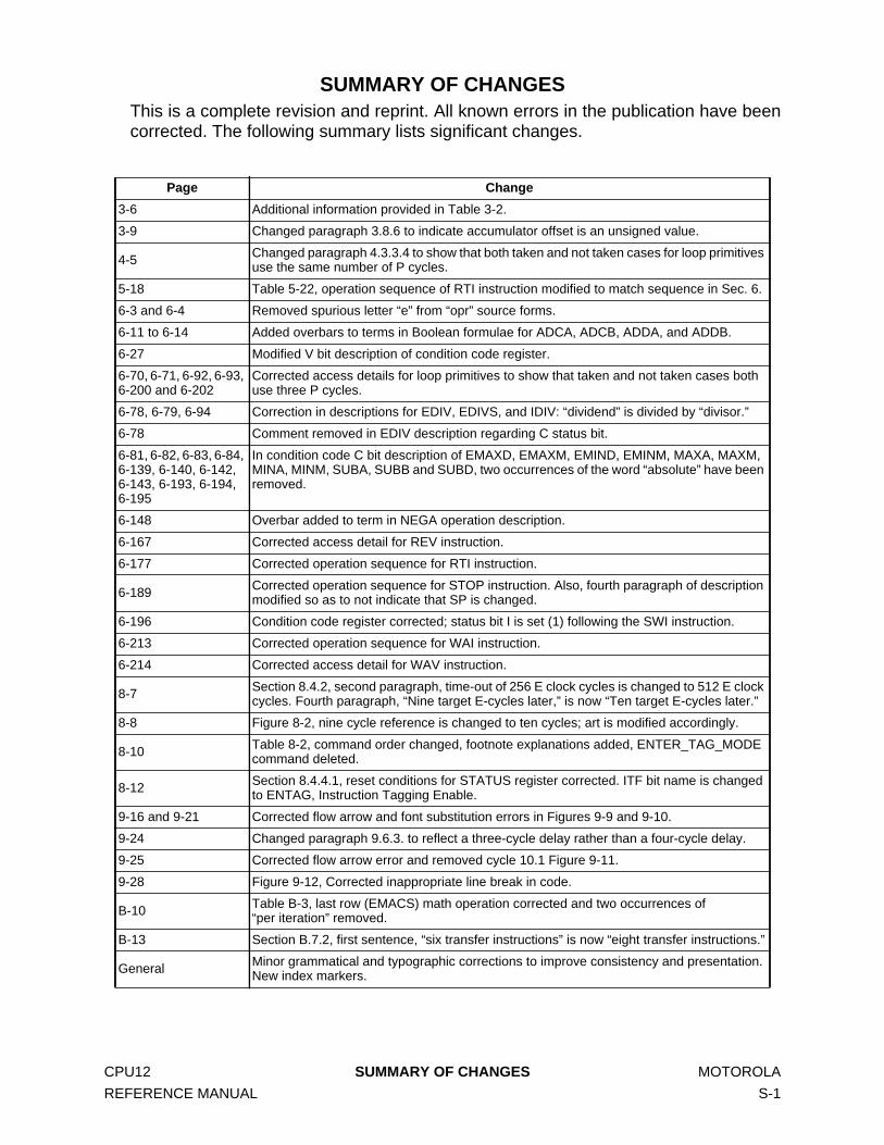
SUMMARY OF CHANGESThis is a complete revision and reprint. All known errors in the publication have beencorrected. The following summary lists significant changes.
Page Change
3-6 Additional information provided in Table 3-2.
3-9 Changed paragraph 3.8.6 to indicate accumulator offset is an unsigned value.
4-5 Changed paragraph 4.3.3.4 to show that both taken and not taken cases for loop primitivesuse the same number of P cycles.
5-18 Table 5-22, operation sequence of RTI instruction modified to match sequence in Sec. 6.
6-3 and 6-4 Removed spurious letter “e” from “opr” source forms.
6-11 to 6-14 Added overbars to terms in Boolean formulae for ADCA, ADCB, ADDA, and ADDB.
6-27 Modified V bit description of condition code register.
6-70, 6-71, 6-92, 6-93,6-200 and 6-202
Corrected access details for loop primitives to show that taken and not taken cases bothuse three P cycles.
6-78, 6-79, 6-94 Correction in descriptions for EDIV, EDIVS, and IDIV: “dividend” is divided by “divisor.”
6-78 Comment removed in EDIV description regarding C status bit.
6-81, 6-82, 6-83, 6-84,6-139, 6-140, 6-142,6-143, 6-193, 6-194,6-195
In condition code C bit description of EMAXD, EMAXM, EMIND, EMINM, MAXA, MAXM,MINA, MINM, SUBA, SUBB and SUBD, two occurrences of the word “absolute” have beenremoved.
6-148 Overbar added to term in NEGA operation description.
6-167 Corrected access detail for REV instruction.
6-177 Corrected operation sequence for RTI instruction.
6-189 Corrected operation sequence for STOP instruction. Also, fourth paragraph of descriptionmodified so as to not indicate that SP is changed.
6-196 Condition code register corrected; status bit I is set (1) following the SWI instruction.
6-213 Corrected operation sequence for WAI instruction.
6-214 Corrected access detail for WAV instruction.
8-7 Section 8.4.2, second paragraph, time-out of 256 E clock cycles is changed to 512 E clockcycles. Fourth paragraph, “Nine target E-cycles later,” is now “Ten target E-cycles later.”
8-8 Figure 8-2, nine cycle reference is changed to ten cycles; art is modified accordingly.
8-10 Table 8-2, command order changed, footnote explanations added, ENTER_TAG_MODEcommand deleted.
8-12 Section 8.4.4.1, reset conditions for STATUS register corrected. ITF bit name is changedto ENTAG, Instruction Tagging Enable.
9-16 and 9-21 Corrected flow arrow and font substitution errors in Figures 9-9 and 9-10.
9-24 Changed paragraph 9.6.3. to reflect a three-cycle delay rather than a four-cycle delay.
9-25 Corrected flow arrow error and removed cycle 10.1 Figure 9-11.
9-28 Figure 9-12, Corrected inappropriate line break in code.
B-10 Table B-3, last row (EMACS) math operation corrected and two occurrences of“per iteration” removed.
B-13 Section B.7.2, first sentence, “six transfer instructions” is now “eight transfer instructions.”
General Minor grammatical and typographic corrections to improve consistency and presentation.New index markers.
CPU12 SUMMARY OF CHANGES MOTOROLA
REFERENCE MANUAL S-1

MOTOROLA SUMMARY OF CHANGES CPU12
S-2 REFERENCE MANUAL


CPU12RM/AD
Motorola reserves the right to make changes without further notice to any products herein. Motorola makes no warranty, representation or guarantee regarding the suitability of itsproducts for any particular purpose, nor does Motorola assume any liability arising out of the application or use of any product or circuit, and specifically disclaims any and all liability,including without limitation consequential or incidental damages. "Typical" parameters which may be provided in Motorola data sheets and/or specifications can and do vary in differentapplications and actual performance may vary over time. All operating parameters, including "Typicals" must be validated for each customer application by customer's technical experts.Motorola does not convey any license under its patent rights nor the rights of others. Motorola products are not designed, intended, or authorized for use as components in systemsintended for surgical implant into the body, or other applications intended to support or sustain life, or for any other application in which the failure of the Motorola product could create asituation where personal injury or death may occur. Should Buyer purchase or use Motorola products for any such unintended or unauthorized application, Buyer shall indemnify and holdMotorola and its officers, employees, subsidiaries, affiliates, and distributors harmless against all claims, costs, damages, and expenses, and reasonable attorney fees arising out of,directly or indirectly, any claim of personal injury or death associated with such unintended or unauthorized use, even if such claim alleges that Motorola was negligent regarding thedesign or manufacture of the part. Motorola and are registered trademarks of Motorola, Inc. Motorola, Inc. is an Equal Opportunity/Affirmative Action Employer.
How to reach us:USA/EUROPE/Locations Not Listed: Motorola Literature Distribution, P.O. Box 5405, Denver, Colorado 80217, 1-800-441-2447 or
1-303-675-2140. Customer Focus Center, 1-800-521-6274JAPAN: Nippon Motorola Ltd.: SPD, Strategic Planning Office, 141, 4-32-1 Nishi-Gotanda, Shinagawa-ku, Tokyo, Japan. 03-5487-8488ASIA/PACIFIC: Motorola Semiconductors H.K. Ltd., 8B Tai Ping Industrial Park, 51 Ting Kok Road, Tai Po, N.T., Hong Kong. 852-26629298Mfax™, Motorola Fax Back System: [email protected]; http://sps.motorola.com/mfax/;
TOUCHTONE, 1-602-244-6609; US and Canada ONLY, 1-800-774-1848HOME PAGE: http://motorola.com/sps/
Mfax is a trademark of Motorola, Inc.
© Motorola, Inc., 1998