cs/ee 3700: fundamentals of digital system design chris j. myers spring 2000 - 2001
TRANSCRIPT

CS/EE 3700: Fundamentals of Digital System Design
Chris J. Myers
Spring 2000 - 2001

Course Information
• Class webpage:– www.async.elen.utah.edu/~myers/ee3700
• Get handout #1 for class and contact info.
• Class webboard – see the webpage

TAs and Grader
• Teaching assistants:– David Sanderson– Jian Zhou– James Bergstrom
• Grader– Dong-Hoon Yoo
• Lots of office hours, see handout #1.

Discussion Sections
• You must signup for and attend one discussion section.
• Supplemental material given here to help with homework and labs.
• Written assignments will be returned in your discussion section.
• Sections start Wednesday.
Course Description
• Boolean algebra – theory for digital design.
• Overview of implementation technology.
• Combinational logic design.
• Number representations and arithmetic.
• Sequential logic design – sync and async.
• VHDL and CAD tools utilized throughout.
Prerequisites
• Computer programming (CS 2010)
• PHYCS 2220
Textbook
• Fundamental of Digital Logic with VHDL Design – by Brown and Vranesic, 2000.
Homework/Labs/Projects
• Homework/lab/project writeups should be turned in to appropriate EE locker.
• Put discussion section number and TA on all assignments.
• Hardware labs checked in discussion section/office hours.
• Homework returned in your discussion section.• All grading disputes must be made within one
week of receiving the grade.

Late Homework/Cheating
• No late homework/labs/projects will be accepted.
• Cheating will be not be tolerated and it will be strongly dealt with. This includes:– Passing off someone else’s hardware as yours.
– Copying someone else’s VHDL code.
– Copying someone’s homework/exam answers.
– etc.
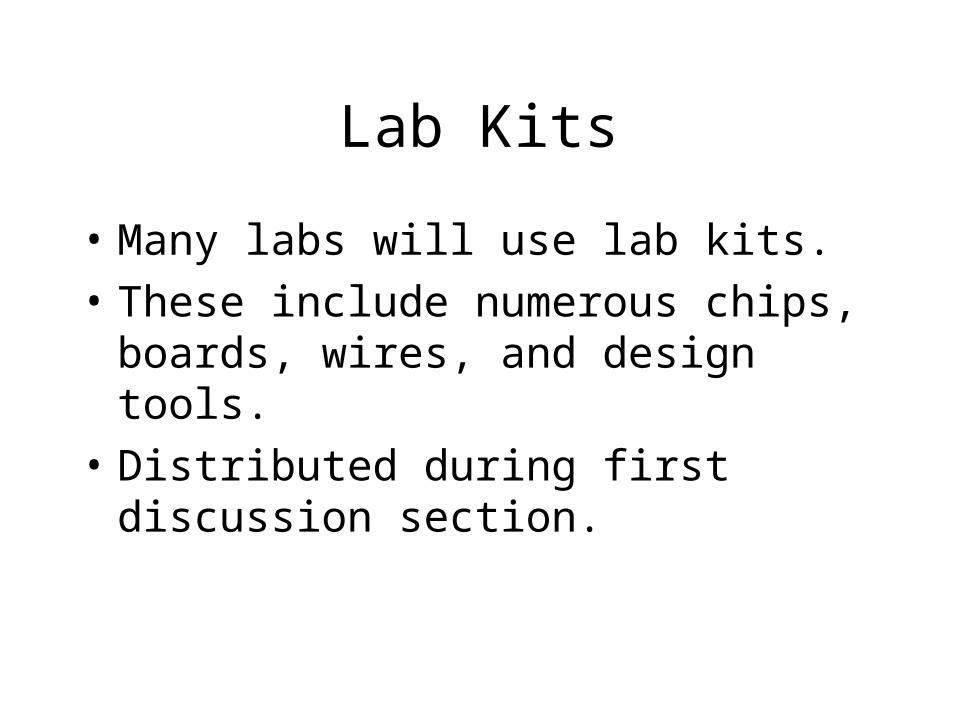
Lab Kits
• Many labs will use lab kits.
• These include numerous chips, boards, wires, and design tools.
• Distributed during first discussion section.
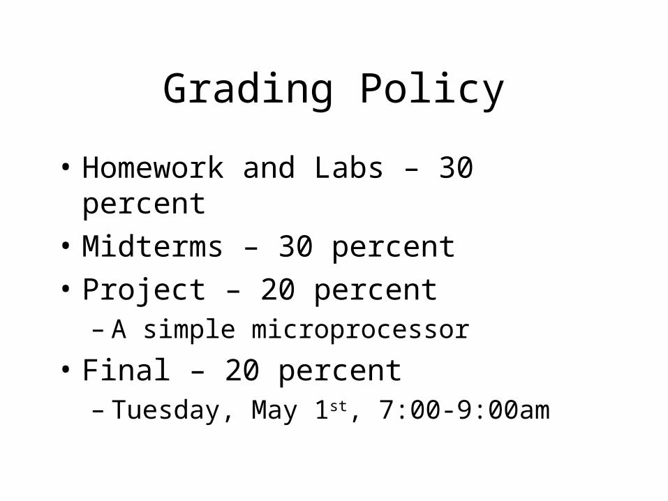
Grading Policy
• Homework and Labs – 30 percent
• Midterms – 30 percent
• Project – 20 percent– A simple microprocessor
• Final – 20 percent– Tuesday, May 1st, 7:00-9:00am
CS/EE 3700 : Fundamentals of Digital System Design
Chris J. Myers
Lecture 1: Design Concepts
Chapter 1
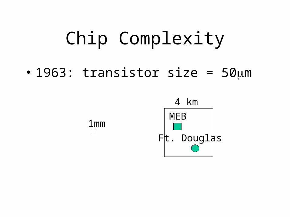
Chip Complexity
• 1963: transistor size = 50m
1mm
4 km
MEB
Ft. Douglas
Chip Complexity
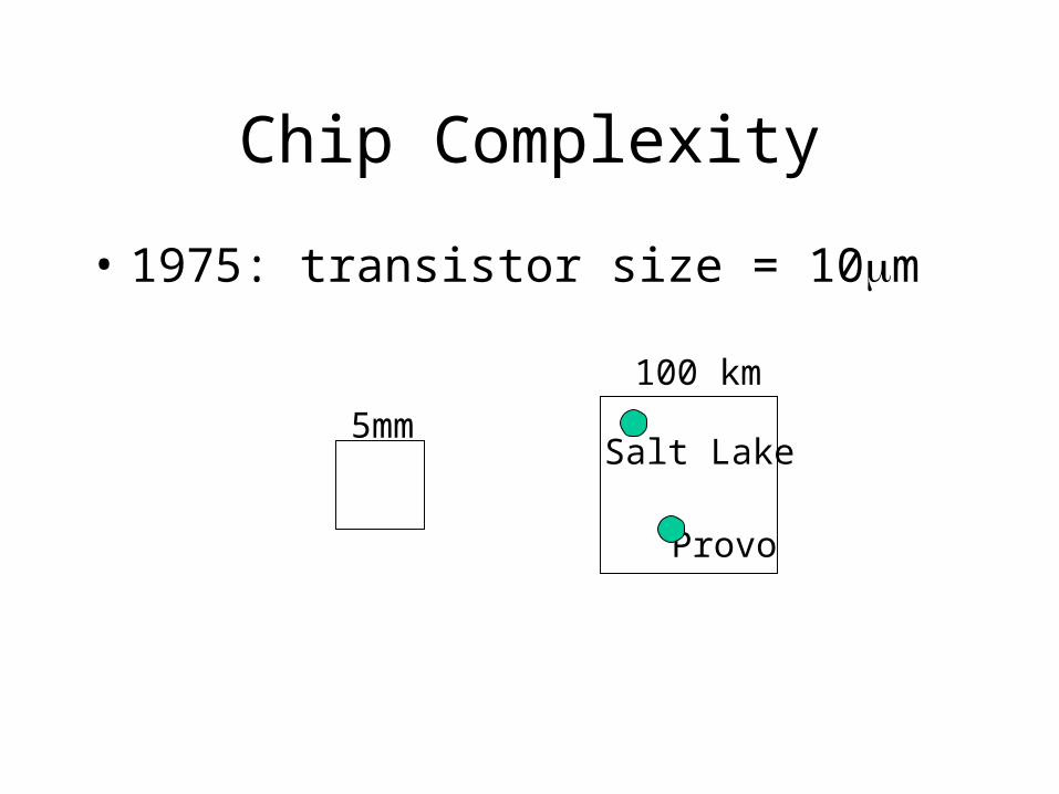
• 1975: transistor size = 10m
5mm
100 km
Salt Lake
Provo
Chip Complexity
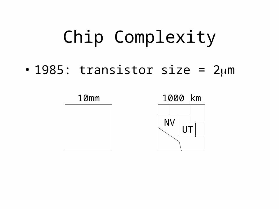
• 1985: transistor size = 2m
10mm 1000 km
NVUT

Chip Complexity
• 1995: transistor size = 0.4m
15mm 7500 km
NorthAmerica

SIA Roadmap
YEAR
1999 2001 2003 2006 2009 2012
xtor size
(m)
0.14 0.12 0.10 0.07 0.05 0.035
xtor/cm2
(million)
14 16 24 40 64 100
Chip size
(mm2)
800 850 900 1000 1100 1300

Figure 1.1 A silicon wafer

Standard Chips
• Realize common logic functions.
• Usually less than 100 transistors.
• Many common ones found in your lab kits.
• You will use them in a couple of labs.
• Not used much today as they occupy too much space on printed circuit boards (PCB).
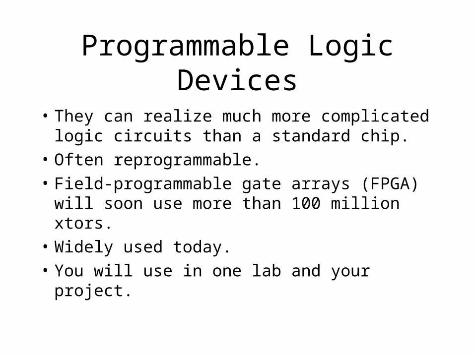
Programmable Logic Devices
• They can realize much more complicated logic circuits than a standard chip.
• Often reprogrammable.
• Field-programmable gate arrays (FPGA) will soon use more than 100 million xtors.
• Widely used today.
• You will use in one lab and your project.

Figure 1.2 A field-programmable gate array chip
Memory blockGroup of 8 logic cells
Interconnectionwires
Custom-designed Chips
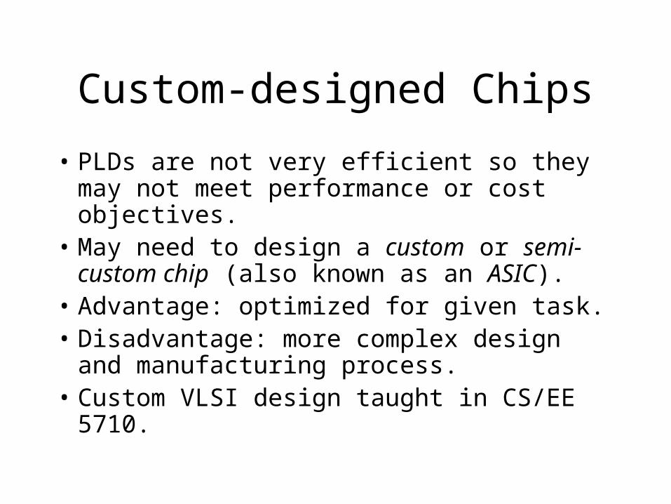
• PLDs are not very efficient so they may not meet performance or cost objectives.
• May need to design a custom or semi-custom chip (also known as an ASIC).
• Advantage: optimized for given task.• Disadvantage: more complex design and
manufacturing process.• Custom VLSI design taught in CS/EE 5710.
Title:(comtest1.ps)Creator:(ImageMagick)Preview:This EPS picture was not savedwith a preview included in it.Comment:This EPS picture will print to aPostScript printer, but not toother types of printers.

Figure 1.3 The development process
Required product
Design specifications
Initial design
Simulation
Design correct?
Redesign
Prototype implementation
Testing
Meets specifications?
Finished product
Minor errors?
Make corrections
No
Yes
No
Yes
Yes
No
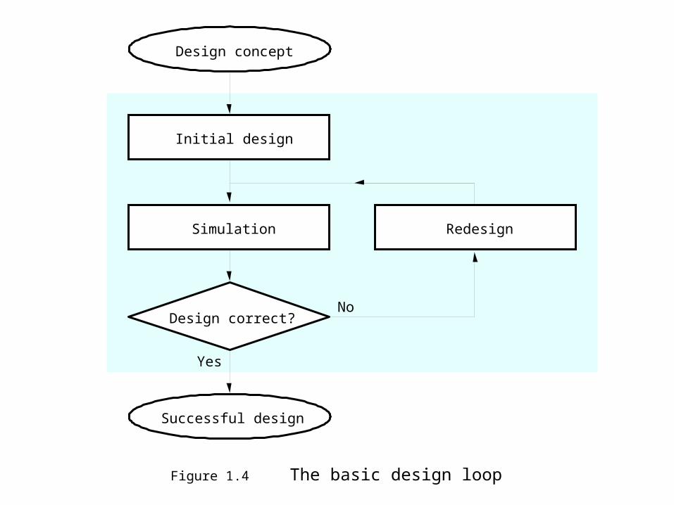
Design concept
Successful design
Initial design
Simulation
Design correct?
Redesign
No
Yes
Figure 1.4 The basic design loop
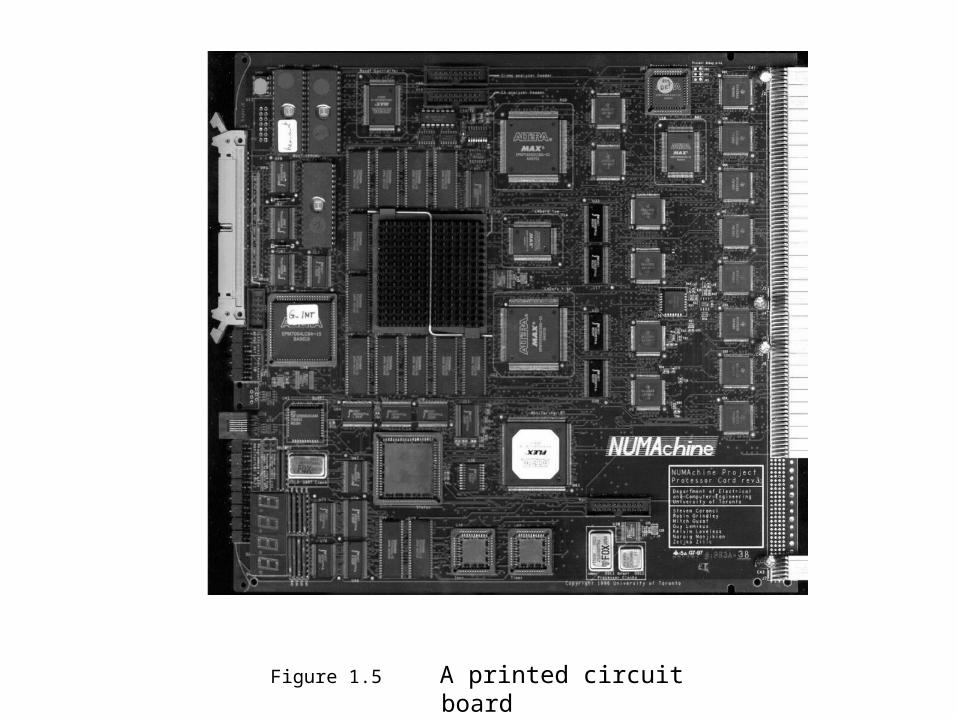
Figure 1.5 A printed circuit board
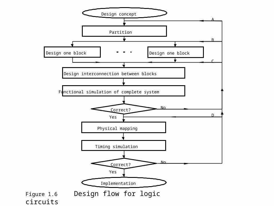
Figure 1.6 Design flow for logic circuits
Design interconnection between blocks
Functional simulation of complete system
Correct?
Physical mapping
Timing simulation
Correct?
Implementation
No
Yes
No
Yes
Design one block Design one block
Partition
Design conceptA
B
C
D
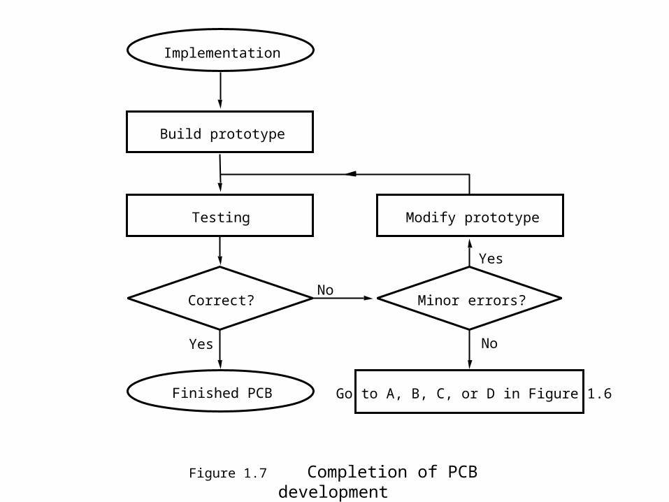
Figure 1.7 Completion of PCB development
Implementation
Finished PCB
Build prototype
Testing
Correct?
Modify prototype
No
Yes
Minor errors?
Yes
Go to A, B, C, or D in Figure 1.6
No

Theory and Practice
• Numerous CAD tools available for design.
• Why study the theory and not just the tools?– Designer must provide good specification.– This theory is utilized in these tools, and it
helps you understand what the tools do.– Designer must understand the effects of
optional processing steps.– It is intellectually challenging.