ct - scientific journal facta universitatis …facta.junis.ni.ac.rs/eae/fu2k13/fu01.pdf · f a ct a...
TRANSCRIPT
FACTA UNIVERSITATIS (NI�S)Series: Electronics and Energetics vol. 14, No. 3, December 2001, 295-327
FIR NOTCH FILTER DESIGN { A REVIEW
Suhash Chandra Dutta Roy, Balbir Kumarand Shail Bala Jain
(Invited Paper)
Abstract: Notch �lters are invariably used in communication, control, in-strumentation, and bio-medical engineering, besides a host of other �elds,to eliminate noise and power line interferences. Digital notch �lters can bedesigned as in�nite impulse response (IIR) as well as �nite impulse response(FIR) structures. As compared to the latter, IIR �lters have the advantagethat they require lower orders for eÆcient approximation of a given set ofspeci�cations. However, IIR �lters are potentially unstable and do not pro-vide linear phase characteristics, in general. FIR �lters, on the other hand,are unconditionally stable and can be designed to give exact linear phasecharacteristics. We, in this review paper, focus our attention to the recentdesign techniques proposed by us for FIR notch �lters.
Standard FIR �lter design methods, such as windowing, frequency samplingand computer-aided/optimization may be used for designing FIR notch �lters.However, most of these methods result in ripples in the passbands. In manysituations, maximally at (MF) �lters are preferred since they have maximumattenuation in the stopband and hence can yield the best signal-to-noise ratio.A number of methods are available in the literature for designing MF digital�lters. We, in this paper, review the design techniques for computing theweights of MF FIR notch �lters. A number of design methodologies havebeen highlighted that lead to either recursive or explicit formulas for thecomputation of weights of FIR notch �lters.
Procedures for the design of FIR notch �lters with maximal atness of theamplitude response (in the Butterworth sense) at ! = 0 and ! = � have
Manuscript received May 12, 2001.S. C. Dutta Roy is with Department of Electrical Engineering, Indian Institute of
Technology (I.I.T. Delhi) Hauz Khas, New Delhi-110016 (e-mail: [email protected]
net.in). B. Kumar is with Department of Electronics and Communication Engineering,Netaji Subhas Institute of Technology (NSIT), Sector-3, Dwarka, New Delhi-110045. S.B.Jain is with Department of Electronics and Communication Engineering, Delhi College ofEngineering (DCE), Bawana Road, New Delhi-110042 (e-mail: [email protected]).
295
296 Facta Universitatis ser.: Elec. and Energ. vol. 14, No. 3, Dec. 2001
been given. Empirical formulas for �nding the �lter length N have also beenproposed. By relaxing the linear phase property, it is possible to reduce the�lter order required for a given magnitude response speci�cations. An FIR�lter (with non-linear phase) can be derived from a second order IIR notch�lter prototype. Explicit mathematical formulas for computing the weightsfor such FIR notch �lters have been given. Design approaches based on theuse of (i) Bernstein polynomials, and (ii) lowpass �lter design have also beenexploited to obtain maximally at FIR notch �lters.
Key words: Digital �lters, FIR �lters, notch �lters.
1. Introduction
1.1 Notch �lters
Digital signal processing (DSP) techniques have rapidly developed inthe recent years due to advances in digital computer technology and inte-grated circuit fabrication [3], [26], [27]. The use of digital circuits yields highspeed as well as high reliability, and also permits us to have programmableoperations. DSP techniques �nd applications in a variety of areas such asspeech processing, data transmission on telephone channels, image process-ing, instrumentation, bio-medical engineering, seismology, oil exploration,detection of nuclear explosion, and in the processing of signals received fromthe outer space, besides others. Various types of digital �lters, such as Low-pass (LP), High-pass (HP), Band-pass (BP), Band-stop (BS), and Notch�lters (NF), and various types of digital operations such as Di�erentiation,Integration and Hilbert transformation, to mention a few, are invariably usedin many of the applications just mentioned. In this review paper, we focusour attention on the design and performance analysis of notch �lters.
1.1.1 Notch �lter characteristics
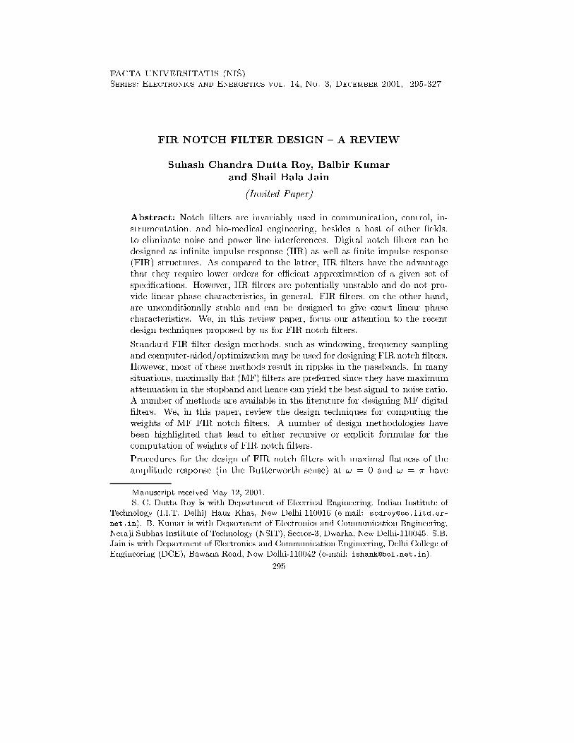
A notch �lter highly attenuates/ eliminates a particular frequency com-ponent from the input signal spectrum while leaving the amplitude of theother frequencies relatively unchanged. A notch �lter is, thus, essentially abandstop �lter with a very narrow stopband and two passbands. The ampli-tude response, H1(!), of a typical notch �lter (designated as NF1) is shownin Fig. 1 and is characterized by the notch frequency, !d (in radians) and 3-dB rejection bandwidth, BW . For an ideal notch �lter, BW should be zero,the passband magnitude should be unity (zero dB) and the attenuation atthe notch frequency should be in�nite.
S.C. Dutta Roy, B. Kumar, S.B. Jain: FIR notch �lter design ... 297
Fig. 1. The amplitude response H1(!) of notch �lter: NF1.
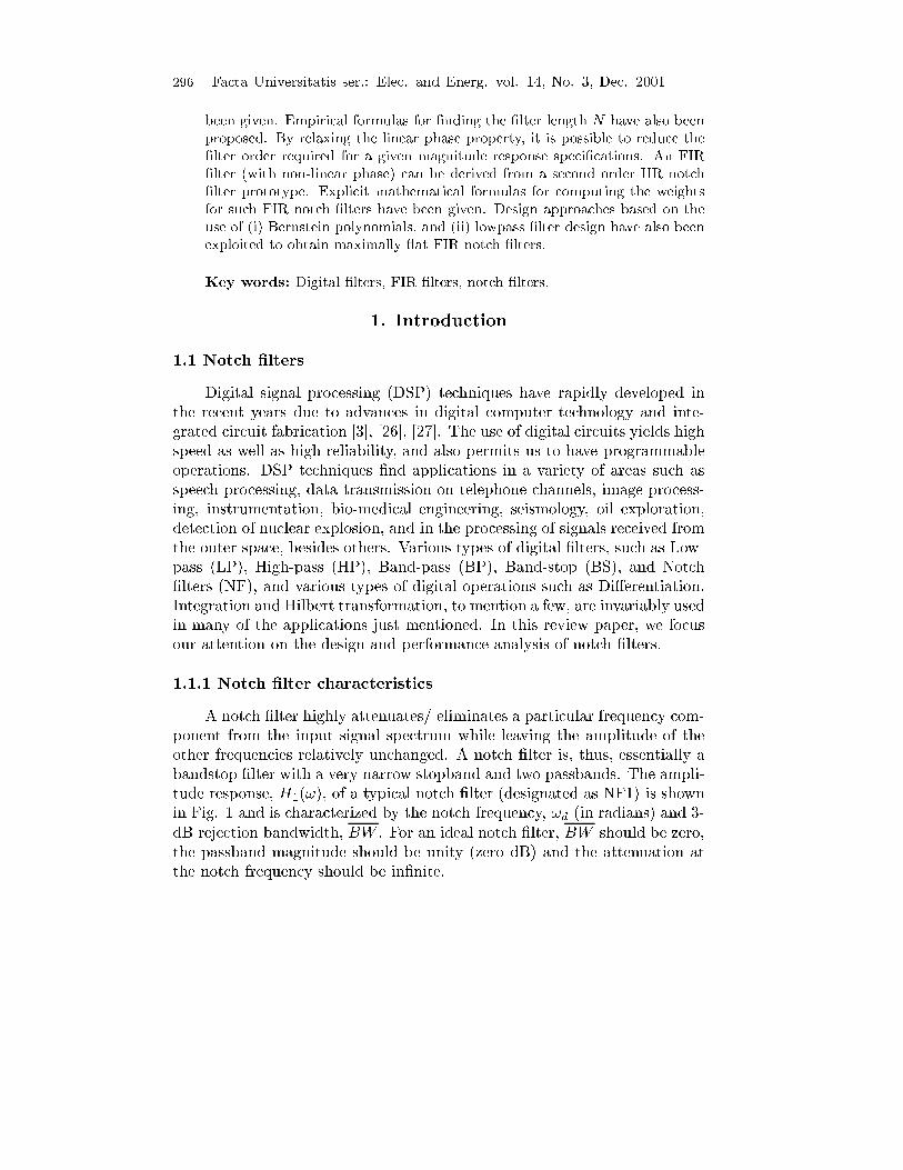
We may, alternatively, have the amplitude response, H2(!), of a notch�lter (designated as NF2) as shown in Fig. 2. H2(!) has 180 degrees phaseshift beyond the notch frequency !d. However, the magnitude responsejH2(!)j is of the same type as that shown in Fig. 1. We review methodologiesfor approximating notch �lters of both the types.
Fig. 2. The response H2(!) and jH2(!)j of notch �lter: NF2.
1.2 Digital notch �lter design techniques
Digital Notch �lters may be designed as in�nite impulse response or�nite impulse response structures by using standard design techniques. Thesalient features of these techniques with speci�c reference to notch �lters willbe brie y discussed.
298 Facta Universitatis ser.: Elec. and Energ. vol. 14, No. 3, Dec. 2001
1.2.1 IIR designs
In situations where linearity of phase is not important, IIR �lters arepreferred since these require much lower order than the FIR ones for thesame set of magnitude response speci�cations. The commonly used IIR �lterdesign methods require transforming the given speci�cations to an equivalentanalog �lter (by using bilinear transformation, for example). We then designthe analog notch �lter and �nally convert it back to the digital domainthrough inverse transformation. This approach has the advantage that thestandard results of analog �lter design can be conveniently used. Based uponthis approach, one may design Butterworth, Chebyshev, or elliptic �lters[24], [26]. Besides these, IIR notch �lters may also be designed by usingPad�e approximation, least-squares approach or �lter parameter optimizationtechniques.
Some modi�ed designs, speci�cally for IIR notch �lters, are also avail-able. Hirano et al. [12] have realized IIR notch �lter function by applyingbilinear transformation on second order analog transfer function. The de-sign requires only two multipliers and o�ers independent variation of notchfrequency (!d) and the 3-dB rejection bandwidth (BW ). Laakso et al. [19]have proposed �rst and second order IIR notch �lters with zeros strictly onthe unit circle and poles close to the zeros to ensure a narrow notch width.The second order notch �lter given by
H(z) = K1� 2 cos!0z
�1 + z�2
1� 2r cos!0z�1 + r2z�2; (1)
can be designed for an arbitrary notch frequency !0. In (1), r is the radiusof the complex conjugate pole pair located at the frequency !0 and K isa scaling factor. In this design, BW can be controlled through r, beingnarrower as r goes closer to the unit circle [19]. However, the quantizationerror increases when � = 1 � jrj is made small (since the variance of thequantization error is proportional to 1=�2 [26]).
In certain applications of signal processing, where it is desired to elim-inate unknown or time-varying narrow-band or sine-wave components fromthe observed time series, we prefer an adaptive notch �lter (ANF). Adaptivenotch �lter designs have been proposed by Thompson [34], Rao and Kung[29], Friedlander and Smith [8], and Nehorai [21], amongst others. Thecomputational eÆciency, stability, convergence and numerical robustness ofthese methods depend upon the algorithm used for adaptation.
One of the major problems in IIR �lters is that these designs have non-linear phase response and, therefore, introduce phase distortion in general.
S.C. Dutta Roy, B. Kumar, S.B. Jain: FIR notch �lter design ... 299
However, it is possible to reduce phase distortion by cascading an all-passphase equalizer.
We now examine some of the design techniques used for FIR notch�lters.
1.2.2 FIR designs
There are essentially three well known classes of design techniques forlinear phase FIR �lters, namely: frequency sampling, windowing, and op-timal (in the Chebyshev sense) design. Frequency sampling method is of-ten not used for notch �lter design because the desired frequency responsechanges radically across the notch point leading to large interpolation error.
The window method is easy to use and closed form expressions are avail-able for the window coeÆcients. Several windows have been reported in theliterature, such as Hamming, Hann, Blackman, Bartlett, Papoulis, Lanczos,Tukey, Kaiser, Dolph-Chebyshev [26] and Prolate Spheroidal wave sequence[32]. These windows o�er various trade-o�s between the 3-dB transitionbandwidth and stopband attenuation. However, \FIR �lters based on thewindow approach do not yield designs which are optimal in any sense, evenif the window is optimal in some sense" [36, p-53].
Vaidyanathan and Nguyen [35] introduced FIR eigen�lters which areoptimal in the least squares sense. Here, the objective function is de�ned onlyas a sum of the passband and stopband errors; the error of approximation inthe transition band is not included. One of the advantages of eigen �lters overother FIR �lters is that they can be designed to incorporate a wide variety oftime domain constraints such as the step response and Nyquist constraint1
in addition to the usual frequency domain characteristics. This method hasalso been extended to include atness constraints in the passband.
Out of all the FIR designs, Parks-McClellan iterative design [25] yieldsthe best results, although, it too has some inherent limitations. Equirippledesigns only consider the speci�ed passbands and stopbands but the transi-tion bands are not considered in the numerical solution. In fact, transitionregions are considered as 'don't care' regions in the design procedure.
As a result, the numerical solution may fail, especially in the transitionregion and for notch �lters in particular. For the optimum design, the �lter
1A Nyquist �lter must satisfy the condition: !p + !s = 2�=k, where !p and !s are,respectively, the passband and stopband edge frequencies and k is the intersymbol timeduration. Such �lters are extensively used in digital modem systems and also in multiratesignal processing [35].
300 Facta Universitatis ser.: Elec. and Energ. vol. 14, No. 3, Dec. 2001
length is determined by the narrower transition band. If the transition bandis wide, the algorithm may fail in the transition region resulting in overshootof the frequency response [6].
Tian-Hu Yu et al. [37] have proposed two methods for designing thenotch �lters by exploiting the aforementioned design techniques. In one ofthe methods, a notch �lter (H(!)) is derived from a lowpass �lter (HLP (!))by using the relation
H(!) = 2HLP (!)� 1: (2)
This transformation provides a change of phase by 180 degrees at thenotch frequency !d i.e. the designed �lter response is of the type NF2 (seeFig. 2). The frequency response H(!) may further be sharpened by usingthe amplitude change function (ACF) [16]. An alternative method in [37]is based on complementing a narrow passband (tone) �lter, B(!), to obtainthe desired notch �lter by using
H(!) = 1�B(!): (3)
Obviously, a narrow-band �lter B(!) will have a large �lter order. Anumber of techniques are, however, available in [1], [4] and [22] for reducingthe number of multiplications.
Another method for designing an FIR notch �lter was proposed byEr [7] where the symmetry constraint for the coeÆcients was relaxed and,therefore, the design yields non-linear phase FIR �lters. Two procedureshave been proposed in [7] for varying the null width. In the �rst approach,the mean squared error between the desired unity response and the responseof the �lter over the frequency band of interest is minimized subject to anull constraint and its zero derivative constraint at the frequency of interest.The null width can be increased in discrete steps by setting more derivativesto zero at the notch frequency.
In the second approach, a null power constraint over a frequency band ofinterest is introduced. This approach is found to be more e�ective in control-ling the null width as compared to the derivative constraint methodology.Both of these approaches adopt optimization techniques which have beeneÆciently solved in [7]. The limitation of such a design, however, is thatit yields non-linear phase and does not provide closed form mathematicalformula for computation of design weights.
FIR �lters �nd extensive use where frequency dispersion due to non-linear phase is undesirable, such as in speech processing, digital communica-tion, image processing, etc.. This is the precise reason that a large number
S.C. Dutta Roy, B. Kumar, S.B. Jain: FIR notch �lter design ... 301
of commercial chips carry out signal processing with FIR �lters. We, in thispaper, discuss some recent design techniques proposed by us, highlightinganalytic designs with recursive as well as explicit mathematical formulasfor computation of the weights required in the design of FIR notch �lters.Also, we have considered notch �lters having maximal atness in the twopassbands, i.e. at ! = 0 as well as at ! = � (in the Butterworth sense).We focus our attention on the design of digital notch �lters of type NF1as well as NF2. Linear phase and also nonlinear phase designs have beeninvestigated.
The transfer function H(z) of a causal FIR �lter of length N in termsof its unit sample response h(i) is given by
H(z) =
N�1Xi=0
h(i)z�i: (4)
For the linear phase requirement, h(i) must satisfy the constraint:
h(i) = �h(N � 1� i); i = 0; 1; 2; : : : ; N � 1 (5)
The �lter length N can be odd or an even integer. However, we chooseN to be an odd integer only so as to avoid problems due to fractional delays.By using (4) and (5), the transfer function of a symmetric linear phase FIR�lter can be written as [24]
H(z) = z�nnXi=0
dizi + z�i
2; n =
N � 1
2(6)
The weights di are related to the unit sample response h(i) by [24]
di =
�h(n); i = 0
2h(n� i); i = 1; 2; : : : ; n(7)
The frequency response H(exp(j!)) of the causal �lter may be writtenas
H(z)���z=ej!
= e�j!nH0(!); (8)
where H0(!) is the amplitude function2 given by
H0(!) =
nXi=0
di cos(i!): (9)
2In the literature amplitude function H0(!) is also referred to as the \pseudo mag-nitude function" or \zero phase amplitude response".

302 Facta Universitatis ser.: Elec. and Energ. vol. 14, No. 3, Dec. 2001
For the design of NF2 type �lters, we impose the following optimalitycriteria:
H0(!)��!=0
= 1; (10a)
H0(!)��!=�
= �1; (10b)
...
duH0(!)
d!u��!=�
= 0; u = 1; 2; : : : ; 2m� 1 (10c)
d�H0(!)
d!���!=0
= 0; � = 1; 2; : : : ; 2(n�m) + 1 (10d)
Here, m is an integer specifying the degree of atness at ! = �, which canhave values within the range 1 � m � n. Equations (10) give us (n+1) non-trivial equations which can be solved to compute the weights (di's). Filtersthus designed are speci�cally useful in applications where linearity of phaseis not an essential requirement. One typical application for such �lters is inone-dimensional QMF banks [36].
Linear phase maximally at notch �lter designs of the type NF1 havealso been accomplished by using Bernstein polynomials as well as by usingnotch �lter to lowpass �lter transformation. These approaches lead to ex-plicit formulas for computation of design weights, as will be shown in thenext section.
2 Designs
2.1 Design of linear phase notch �lter:Analytical approach [30]
In the methods presented in [7], [37], the weights required for the �lterstructure are found by using computer-aided optimization techniques. How-ever, by an analytical formulation of this problem, it is possible to �nd theexact mathematical formula for the weights. We choose the optimality crite-ria of maximal atness of the amplitude response (in the Butterworth sense)at ! = 0 and ! = � as given by (10). Such a choice leads us to exact mathe-matical formulas for computing the design weights. It has been shown in [30]that through this methodology, it is possible to realize, exactly, the desirednotch frequency, !d, besides meeting the speci�ed rejection bandwidth BW .
S.C. Dutta Roy, B. Kumar, S.B. Jain: FIR notch �lter design ... 303
2.1.1 Design
Let the frequency response, Hd(!), of the desired FIR digital notch�lter be given by
Hd(!) =
N�1Xi=0
h(i)ej!i; (11)
where h(i) is the impulse response and N is the �lter length, the �lter orderbeing N � 1. Imposing symmetry condition, we have [24]
h(i) = �h(N � 1� i): (12)
The design requirement is to have non-zero Hd(!) both at ! = 0 and! = �. Hence, we take the positive sign in (12) so as to obtain a cosineseries. Imposing (12) on (11) and keeping N odd, we obtain
hd(!) = e�j!(N�1)
2
N�12X
i=0
Di cos(i!); (13a)
where
D0 =h(N � 1
2); (13b)
Di =2h(N � 1
2� i); i = 1; 2; : : : ;
N � 1
2(13c)
We derive the desired Hd(!) through the use of two maximally atnotch �lters belonging to the class Hm(!), each of order N � 1, such that:
(i) Hm(!) has m degrees of atness at ! = � where m can assume(N � 1)=2 di�erent integer values;
(ii) the notch frequency of Hm(!) is !m i.e. Hm(!m) = 0; and
(iii) Hm(!) is positive for 0 � ! < !m and negative for !m < ! � �.
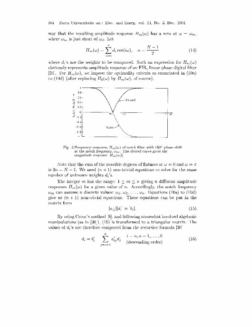
A typical amplitude response of the notch �lter Hm(!) satisfying theabove constraints is shown in Fig. 3 and has 180Æ phase shift at the notchfrequency, !m. The reason for taking such a response is to evade disconti-nuities of Hm(!) at ! = !m; also it yields exact formulas for computationof the weights required for Hm(!). As is clear from Fig. 3, the magnituderesponse jHm(!)j is that of a typical notch �lter. We choose m in such a
304 Facta Universitatis ser.: Elec. and Energ. vol. 14, No. 3, Dec. 2001
way that the resulting amplitude response Hm(!) has a zero at ! = !m,where !m is just short of !d. Let
Hm(!) =nXi=0
di cos(i!); n =N � 1
2(14)
where di's are the weights to be computed. Such an expression for Hm(!)obviously represents amplitude response of an FIR, linear phase digital �lter[24]. For Hm(!), we impose the optimality criteria as enunciated in (10a)to (10d) (after replacing H0(!) by Hm(!), of course).
Fig. 3.Frequency response, Hm(!) of notch �lter with 180Æ phase shiftat the notch frequency, !m. The dotted curve gives themagnitude response jHm(!)j.
Note that the sum of the possible degrees of atness at ! = 0 and ! = �is 2n = N � 1. We need (n+ 1) non-trivial equations to solve for the samenumber of unknown weights di's.
The integer m has the range: 1 � m � n giving n di�erent amplituderesponses Hm(!) for a given value of n. Accordingly, the notch frequency!m can assume n discrete values: !1, !2, : : : , !n. Equations (10a) to (10d)give us (n + 1) non-trivial equations. These equations can be put in thematrix form
[aij ][di] = [bi]: (15)
By using Crout's method [9], and following somewhat involved algebraicmanipulations (as in [30]), (15) is transformed to a triangular matrix. Thevalues of di's are therefore computed from the recursive formula [30]
di = b0i �nX
j=i+1
a0ijdji = n; n� 1; : : : ; 0
(descending order)(16)
S.C. Dutta Roy, B. Kumar, S.B. Jain: FIR notch �lter design ... 305
where the values of b0i and a0ij are given by exact mathematical formulas [30].
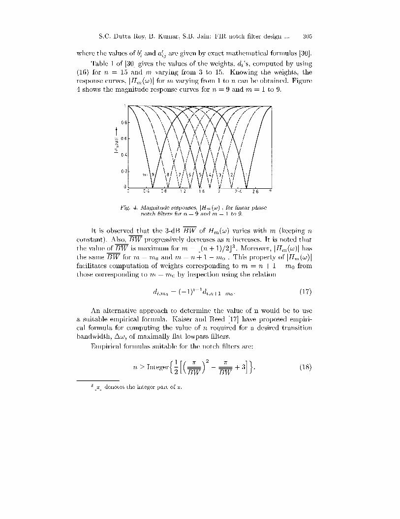
Table 1 of [30] gives the values of the weights, di's, computed by using(16) for n = 15 and m varying from 3 to 15. Knowing the weights, theresponse curves, jHm(!)j for m varying from 1 to n can be obtained. Figure4 shows the magnitude response curves for n = 9 and m = 1 to 9.
Fig. 4. Magnitude responses, jHm(!)j, for linear phasenotch �lters for n = 9 and m = 1 to 9.
It is observed that the 3-dB BW of Hm(!) varies with m (keeping nconstant). Also, BW progressively decreases as n increases. It is noted thatthe value of BW is maximum for m = b(n+1)=2c3. Moreover, jHm(!)j hasthe same BW for m = m0 and m = n+ 1�m0 . This property of jHm(!)jfacilitates computation of weights corresponding to m = n + 1 � m0 fromthose corresponding to m = m0 by inspection using the relation
di;m0= (�1)i+1di;n+1�m0
: (17)
An alternative approach to determine the value of n would be to usea suitable empirical formula. Kaiser and Reed [17] have proposed empiri-cal formula for computing the value of n required for a desired transitionbandwidth, �!, of maximally at lowpass �lters.
Empirical formulas suitable for the notch �lters are:
n � Integern12
h� �
BW
�2�
�
BW+ 3
io; (18)
3bxc denotes the integer part of x.
306 Facta Universitatis ser.: Elec. and Energ. vol. 14, No. 3, Dec. 2001
and
m1 = Integer part offn(0:55 + 0:5 cos!d)g: (19)
Formula (19) has been arrived at after modifying an existing formula,due to Herrmann [11], for maximally at lowpass �lters of order n and 3-dBcuto� frequency, !c, viz.
m = Integer � n1 + cos!c
2: (20)
The formulas given by (18) and (19) hold good for �lter lengths up to79.
We design Hm1(!) and Hm2
(!), where m2 = m1 � 1, and obviously!m1
< !d < !m2. To obtain desired notch �lter Hd(!) with notch at
! = !d, we use linear mixing of Hm1(!) and Hm2
(!), i.e.
Hd(!) = �Hm1(!) + �Hm2
(!); (21a)
where
� =!m2
� !d!m2
� !m1
; (21b)
and
� =!d � !m1
!m2� !m1
: (21c)
The weights of the desired notch �lters are given by
Di = �d(m1)i + �d
(m2)i : (22)
Note that � and � satisfy the condition: � + � = 1; also to ensure thatHd(0) = �Hd(�) = 1, we should have
�
�=���Hm2
(!d)
Hm1(!d)
���: (23)
The aforementioned procedure indeed yields the notch frequency ofHd(!), that is very close to the desired one (!d). The design also retains themaximal atness of the passbands and achieves an exact null at the notchfrequency. The mathematical formulas for computing the weights neededconstitute an attractive feature of this design.
S.C. Dutta Roy, B. Kumar, S.B. Jain: FIR notch �lter design ... 307
The rejection bandwidth BW can be made small if suÆciently highvalue of n is chosen. For a given n, this �lter provides a �xed range of notchfrequencies, varying from !djm=n to !djm=1.
In this procedure, we need a linear combination of Hm1(!) and Hm2
(!),in order to arrive at the desired response Hd(!). The value of Hd(!d) is notexactly zero; hence �ne tuning is essential to obtain the �nal response Hd(!)[30]. In the next design, we suggest a semi-analytic method of notch �lterdesign which eliminates the necessity of linear mixing as well as that of the�ne tuning.
2.2 A semi-analytic approach for designingFIR notch �lter [14]
In this approach, the desired notch �lter can be designed directly, with-out the need for combination of two �lters or the requirement of �ne tuning.The design requires less number of weights as compared to the analytic ap-proach, given in subsection 2.1.
Let the amplitude response, Hd(!), of a typical linear phase FIR digitalnotch �lter be given by [24]
Hd(!) =
L�12X
i=0
Di cos(i!); (24)
where Di's are the weights4 to be computed, and L is the length of the �lter
(assumed to be odd ). We let Hd(!) satisfy the criteria (10a) to (10d) andalso the additional constraint:
Hd(!d) = 0: (25)
The constraint (25) is taken care of by increasing the �lter length toN = L + 2. It may be noted that, to retain linear phase property of thenotch �lter, we have increased the length by 2 to obtain one additional non-trivial equation. By using (25) in (24) and taking n = (N � 1)=2, we have
nXi=0
Di cos(i!d) = 0; (26)
4Note that the weights Di's used here are not the same as those found in the de-sign given in subsection 2.1 by linear mixing. The notation (Di) has been retained forconvenience.

308 Facta Universitatis ser.: Elec. and Energ. vol. 14, No. 3, Dec. 2001
ornXi=0
CiDi = 0; (27)
where
Ci4=cos(i!d); i = 0; 1; 2; : : : ; n (28)
Imposing the optimality criteria (10a to 10d) on Hd(!) and by using(27), we obtain a set of (n + 1) non-trivial equations. These equationsare again solved by using Crout's method. Here, the recursive mathematicalformulas are obtained after somewhat involved manipulation [14]. The valueof n is again found preferably by using the empirical formula (18) and m isfound from
m =
�bn(0:55 + 0:5 cos!d)c; 1 � n � 20
bn(0:55 + 0:5 cos!d)� 1c; n > 20(29)
where bxc denotes the integer part of x. The values of n and m found byabove empirical formulas hold good up to N = 65. A design example maybe referred to in [14].
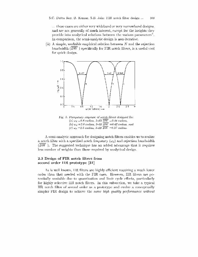
The magnitude responses of a few other notch �lters designed by usingthe proposed algorithm are shown in Fig. 5. The speci�ed and the realizedvalues of various parameters for these designs are given in [14]. It is seenthat in all these designs, we are able to realize the exact notch frequency(!d). Also, the realized BW is lower than the speci�ed value. This con�rmsthe eÆcacy of the suggested methodology.
The proposed design method has been found to give the desired fre-quency response for �lter length N upto 65. Beyond this value of N , it hasbeen observed that a small content of ripple appears in the response. Wenote that the FIR notch �lters can also be designed by McClellan and Parksalgorithm to obtain equiripple (i.e. minimax) frequency response. We des-ignate such a design by HEQ(!). If we compare the performance of notch�lters Hd(!) with that of �lters HEQ(!), we �nd that the 3-dB bandwidth
(BW ) is certainly lower in the case of minimax design, as expected. Wealso note that:
(i) Equiripple/Minimax design using Remez algorithm (i.e. McClellanand Parks approach) is basically iterative in nature and is non-analytic. As pointed out by Rabiner et al., in [28], \An analyticalsolution to the optimal �lter design problem exists for the case ofextra-ripple design with either one passband or one stopband ripple.
S.C. Dutta Roy, B. Kumar, S.B. Jain: FIR notch �lter design ... 309
... these cases are either very wideband or very narrowband designs,and are not generally of much interest, except for the insights theyprovide into analytical relations between the various parameters".In comparison, the semi-analytic design is non-iterative.
(ii) A simple, workable empirical relation between N and the rejectionbandwidth (BW ) speci�cally for FIR notch �lters, is a useful toolfor quick design.
Fig. 5. Ferequency response of notch �lters designed for:(a) !d =0.8 radian, 3-dB BW =0.44 radian,
(b) !d =2.0 radian, 3-dB BW =0.42 radian, and
(c) !d =2.5 radian, 3-dB BW =0.37 radian.
A semi-analytic approach for designing notch �lters enables us to realizea notch �lter with a speci�ed notch frequency (!d) and rejection bandwidth(BW ). The suggested technique has an added advantage that it requiresless number of weights than those required by analytical design.
2.3 Design of FIR notch �lters fromsecond order IIR prototype [31]
As is well known, IIR �lters are highly eÆcient requiring a much lowerorder than that needed with the FIR ones. However, IIR �lters are po-tentially unstable due to quantization and limit cycle e�ects, particularlyfor highly selective IIR notch �lters. In this subsection, we take a typicalIIR notch �lter of second order as a prototype and evolve a conceptuallysimpler FIR design to achieve the same high quality performance without
310 Facta Universitatis ser.: Elec. and Energ. vol. 14, No. 3, Dec. 2001
any instability problem. As will be seen, the frequency response of the de-rived FIR notch �lter is indeed very close to that of the prototype IIR notch�lter. Mathematical formulas for computing the design weights have alsobeen suggested. These formulas take less time for computing the weights ascompared to the designs discussed in subsections 2.1 and 2.2.
2.3.1 The prototype IIR notch �lter
IIR digital notch �lters can be designed by using classical analog �lterapproximation methods. However, one is likely to face two types of problems[24] in such designs. The design program requires passband and stopbandedge frequencies and ripples as input parameters, and choice of improperspeci�cations can lead to high orders of the �lters. Also, for the design ofdigital narrow-band notch �lters, the z-domain poles tend to be very closeto the unit circle. This results in a highly non-linear phase response, highround-o� noise and potential instability/limit cycles in �nite wordlengthimplementations.
A simpler design strategy proposed by Laakso et al. [19] is to design�rst and second order IIR prototype notch �lters with zeros strictly on theunit circle and poles close to the zeros.
A second order IIR notch �lter is, however, more versatile since it canbe designed for an arbitrary notch frequency, !0. A typical such �lter hasthe transfer function [19]:
F2(z) = K1� 2 cos!0z
�1 + z�2
1� 2r cos!0z�1 + r2z�2: (30)
K and r are the parameters as stated earlier. The notch e�ect in (30) isobtained by placing a pair of complex conjugate zeros at exp(�j!0) whilethe frequency response in the passband is made close to unity by placing apair of conjugate poles at r exp(�j!0), where r is less than unity but veryclose to it. Figure 6 shows the magnitude response of second order IIR notch�lter for r varying from 0.9 to 0.99. The 3-dB rejection bandwidth (BW) of these �lters is a function of r and can be reduced by increasing thepole radius r. However, if r is chosen too close to unity, the round-o� noise,which is proportional to 1=�2 (� = 1 � r) [5], becomes very large. For�nite wordlengths, these �lters also introduce limit cycle problems. This isthe precise reason that in many practical applications, we use FIR �lters inpreference to IIR ones. We, in this design, present two design alternativesfor evolving FIR notch �lters from the second order IIR prototype given by(30).

S.C. Dutta Roy, B. Kumar, S.B. Jain: FIR notch �lter design ... 311
Fig. 6. Magnitude response of second order IIR notch �lter [19]having !0 = 1:2 rads for r = 0:90 (curve a), 0.95 (curve b)and 0.99 (curve c).
2.3.2 FIR design: Approach - I
We rewrite (30) as
F2(z) = KA(z)B(z); (31a)
where
A(z) =1� 2 cos!0z�1 + z�2; (31b)
B(z) =1
1� az�1 + bz�2; (31c)
witha = 2r cos!0 and b = r2: (31d)
Clearly,A(ej!) =1� 2 cos!0e
�j! + e�j2!
=e�j2!(ej! � ej!0)(ej! � e�j!0):(32)
Dividing 1 by (1�az�1+bz�2), B(z) given in (31c) may be expressed asa series with increasing powers of z�1. After simple algebraic manipulations,we get the following elegant form for B(z)
B(z) =
1Xi=0
diz�i; (33)
312 Facta Universitatis ser.: Elec. and Energ. vol. 14, No. 3, Dec. 2001
where
di =
b i2 cXm=0
(�1)m�i�m
m
�ai�2mbm; i = 0; 1; 2; : : : ; (34)
In order to arrive at an FIR structure, we truncate the series for B(z),given in (33), at the i =M term, say, i.e. we approximate B(z) by
BM (z) =
MXi=0
diz�i; (35)
where the coeÆcients (di's) are functions of r and !0 only and are indepen-dent of M . This property of di's enables us to control BW for a given !0and M only by varying r. The resulting FIR �lter has the transfer functionH(z) = KA(z)BM (z). Clearly, H(z) is of order N =M + 2. The frequencyresponse H(exp(j!)) can be readily put in the form
H(ej!) = 2K(cos! � cos!0)e�j!
MXi=0
die�j!i; (36)
which is obviously constrained to have a zero (notch) at ! = !0. We mayalso write
H(z) = KNXi=0
Diz�i; (37)
whereDi = di � 2di�1 cos!0 + di�2; (38)
with dk = 0 for k < 0 and k > M . The design weight, Di's, for the proposedFIR notch �lter can thus be computed exactly from (34) and (38). We shallinvestigate the performance of this design after subsection 2.3.3.
2.3.3 FIR design: Approach - II
In the aforementioned treatment, we have truncated the series for B(z)only (keeping A(z) unaltered). Such an approach, obviously, gives an exactzero for H(exp(j!)) at ! = !0. Alternatively, we �rst express F2(z) as aseries of in�nite number of terms, and then truncate this series. Clearly,this will not make H(exp(j!0)) exactly equal to zero, but this approach hasother advantages over the previous one.
S.C. Dutta Roy, B. Kumar, S.B. Jain: FIR notch �lter design ... 313
Writing (31a) in the form
F2(z) =K(1� 2 cos!0z�1 + z�2)
1Xi=0
diz�i
=K
1Xi=0
�Diz�i;
(39)
where�Di = di � 2di�1 cos!0 + di�2; i = 0:1; 2; : : : ; (40)
and dk = 0 for k < 0. By using (34) and (40), we arrive at the followingexplicit formula for �Di : [31]
�Di =
b i2�1cXi=0
Q(i;m) + C(i); i = 0; 1; 2; : : : ; (41a)
where
Q(i;m) =(�1)m(2r cos!0)i�2mr2m
"�i�m
m
�
+ (2r cos!0)�2
�i� 2�m
m
�� r�1
�i� 1�m
m
�#;
(41b)
and
C(i) =
8><>:
0; i = 0; 1
(�1)i2 ri; i = 2; 4; 6; : : : ;
(�1)i�12 [(i+ 1)r � 2]ri�1 cos!0; i = 3; 5; 7; : : : ;
(41c)
An N -th order notch �lter, �H(z), is obtained by truncating the seriesgiven by (39) at i = N term, that is
�H(z) = K
NXi=0
�Diz�i: (42)
The performance of this FIR notch �lter [ �H(z)] is given in the next Sec-tion, and compared with that of the �ltersH(z) derived through Approach-I.

314 Facta Universitatis ser.: Elec. and Energ. vol. 14, No. 3, Dec. 2001
2.3.4 Performance of design: - Approaches I & II
The performance of the notch �lters designed by using the aforemen-tioned designs ( Approaches I and II) has been investigated in respect of
(i) magnitude response,
(ii) relative deviation, and
(iii) group delay
(A) Magnitude response:
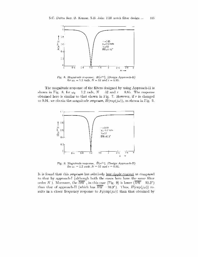
The magnitude response jH(exp(j!)j with M = 50 (i.e. �lter orderN = 52), r = 0:85 and !0 = 1:2 rads obtained through (37) (i.e. ApproachI) is shown in Fig. 7. For comparison, the magnitude response jF2(exp(j!))jof the IIR �lter designed by using (30) (i.e. the prototype �lter) for the samevalues of r and !0 is also shown on the same �gure. It is seen that the twomagnitude responses viz. jH(exp(j!))j and jF2(exp(j!))j are indistinguish-ably close to each other over the entire frequency range 0 � ! � �. Thisindicates that the truncation of the system response B(z) at M = 50 hasnot a�ected the magnitude response jF2(exp(j!))j signi�cantly. The 3-dBrejection bandwidth (BW ) in this case (for N = 52, r = 0:85, !0 = 1:2rads, for example) is found to be 0.3089 rad (= 17:7Æ). In order to obtainstill lower values of BW , we may increase the value of r. For r = 0:91,N = 52, and the same notch frequency (i.e. !0 = 1:2 rads, for example), thevalue of BW is found to be 0.19 rad (= 10:9Æ ).
Fig. 7. Magnitude response, jH(ej!j, (Design Approach-I)for !0 = 1:2 rads, N = 52 and r = 0:85.The magnitude response jF2(ej!)j overlaps jH(ej!)jindistinguishably.
S.C. Dutta Roy, B. Kumar, S.B. Jain: FIR notch �lter design ... 315
Fig. 8. Magnitude response, j �H(ej!j, (Design Approach-II)for !0 = 1:2 rads, N = 52 and r = 0:85.
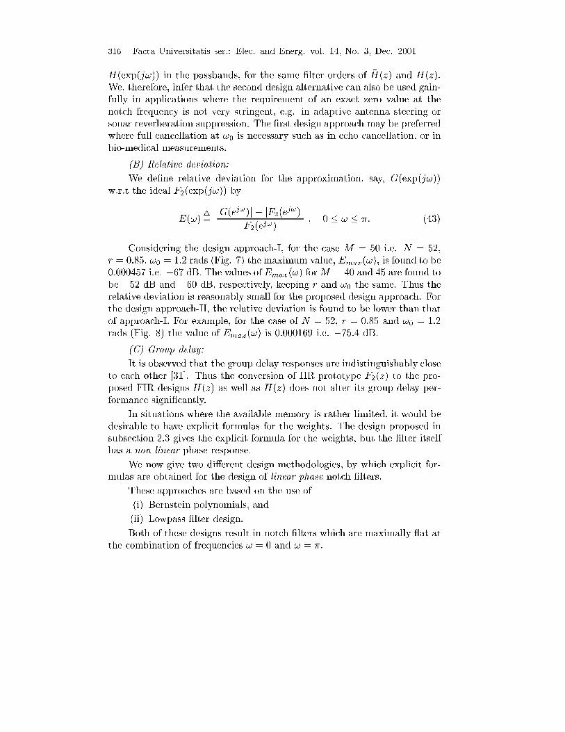
The magnitude response of the �lters designed by using Approach-II isshown in Fig. 8, for !0 = 1:2 rads, N = 52 and r = 0:85. The responseobtained here is similar to that shown in Fig. 7. However, if r is changedto 0.91, we obtain the magnitude response, �H(exp(j!)), as shown in Fig. 9.
Fig. 9. Magnitude response, j �H(ej!j, (Design Approach-II)for !0 = 1:2 rads, N = 52 and r = 0:91.
It is found that this response has relatively less ripple content as comparedto that by approach-I (although both the cases here have the same �lterorder N ). Moreover, the BW , in this case (Fig. 9) is lower (BW =10:3Æ)than that of approach-II (which has BW =10:9Æ). Thus, �H(exp(j!)) re-sults in a closer frequency response to F2(exp(j!)) than that obtained by
316 Facta Universitatis ser.: Elec. and Energ. vol. 14, No. 3, Dec. 2001
H(exp(j!)) in the passbands, for the same �lter orders of �H(z) and H(z).We, therefore, infer that the second design alternative can also be used gain-fully in applications where the requirement of an exact zero value at thenotch frequency is not very stringent, e.g. in adaptive antenna steering orsonar reverberation suppression. The �rst design approach may be preferredwhere full cancellation at !0 is necessary such as in echo cancellation, or inbio-medical measurements.
(B) Relative deviation:
We de�ne relative deviation for the approximation, say, G(exp(j!))w.r.t the ideal F2(exp(j!)) by
E(!)4=
����� jG(ej!)j � jF2(e
j!)j
F2(ej!)
�����; 0 � ! � �: (43)
Considering the design approach-I, for the case M = 50 i.e. N = 52,r = 0:85, !0 = 1:2 rads (Fig. 7) the maximum value, Emax(!), is found to be0.000457 i.e. �67 dB. The values of Emax(!) forM = 40 and 45 are found tobe �52 dB and �60 dB, respectively, keeping r and !0 the same. Thus therelative deviation is reasonably small for the proposed design approach. Forthe design approach-II, the relative deviation is found to be lower than thatof approach-I. For example, for the case of N = 52, r = 0:85 and !0 = 1:2rads (Fig. 8) the value of Emax(!) is 0.000169 i.e. �75:4 dB.
(C) Group delay:
It is observed that the group delay responses are indistinguishably closeto each other [31]. Thus the conversion of IIR prototype F2(z) to the pro-posed FIR designs H(z) as well as �H(z) does not alter its group delay per-formance signi�cantly.
In situations where the available memory is rather limited, it would bedesirable to have explicit formulas for the weights. The design proposed insubsection 2.3 gives the explicit formula for the weights, but the �lter itselfhas a non-linear phase response.
We now give two di�erent design methodologies, by which explicit for-mulas are obtained for the design of linear phase notch �lters.
These approaches are based on the use of
(i) Bernstein polynomials, and
(ii) Lowpass �lter design.
Both of these designs result in notch �lters which are maximally at atthe combination of frequencies ! = 0 and ! = �.

S.C. Dutta Roy, B. Kumar, S.B. Jain: FIR notch �lter design ... 317
2.4 Design of FIR notch �lters by usingBernstein polynomials [15]
Here, we use Bernstein polynomials to derive an explicit formula forthe weights. This has been possible by expressing the transfer function ofthe �lter as a polynomial in cos!. Transfer functions expressed in thisform are particularly convenient for implementing variable cuto� �lters [23].We have used Bernstein polynomials because they \mimic the behavior ofthe function to a remarkable degree" [5, p.116]. Bernstein polynomials arealso well known to yield smooth approximations, in contrast to Chebyshevapproximations (which is characterized by ripple behaviour). Hence, thesepolynomials provide an easy method for approximating a function in themaximally at manner (in the Butterworth sense).
2.4.1 Design
We aim to approximate an ideal notch �lter, Hd(!) given by
Hd(!)4=
�+1; j!j < !d
�1; !d < j!j < �(44)
by using Bernstein polynomials. Consider a function f(x) de�ned in theinterval [0, 1], as shown in Fig. 10, with functional values given by
f(k
n)4=
�+1; 0 � k � L
�1; L+ 1 � k � n(45)
where L+1 and n�L give the number of successive discrete points at whichthe function f(k=n) is +1 and �1, respectively. The n-th order (n � 1)Bernstein polynomial for the function f(x) is given by [5]
Bn(x) =
nXk=0
f(k
n)
�n
k
�xk(1� x)n�k: (46)
An alternate expression for (46) is
Bn(x) =
nXk=0
�kf(0)
�n
k
�xk; (47)
where �kf(0) is the k-th forward di�erence of f(k=n) at k = 0, and isdetermined from its functional values at k = 0; 1; 2; : : : ; n. From (46), we
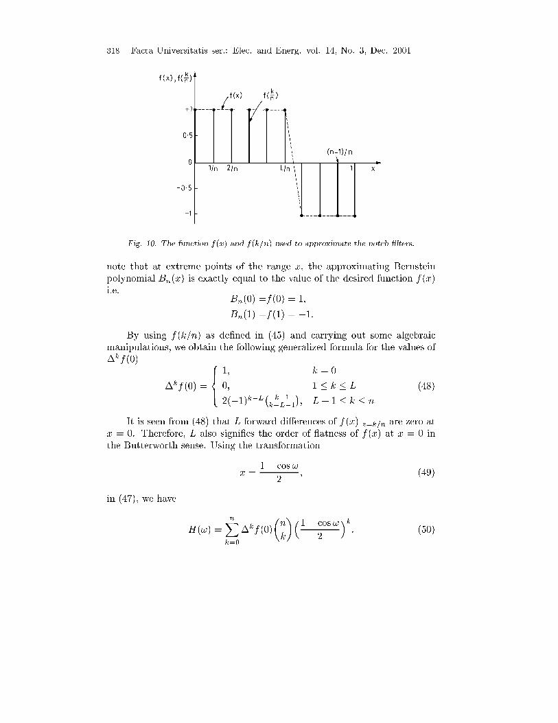
318 Facta Universitatis ser.: Elec. and Energ. vol. 14, No. 3, Dec. 2001
Fig. 10. The function f(x) and f(k=n) used to approximate the notch �lters.
note that at extreme points of the range x, the approximating Bernsteinpolynomial Bn(x) is exactly equal to the value of the desired function f(x)i.e.
Bn(0) =f(0) = 1;
Bn(1) =f(1) = �1:
By using f(k=n) as de�ned in (45) and carrying out some algebraicmanipulations, we obtain the following generalized formula for the values of�kf(0)
�kf(0) =
8><>:
1; k = 0
0; 1 � k � L
2(�1)k�L�
k�1k�L�1
�; L+ 1 � k � n
(48)
It is seen from (48) that L forward di�erences of f(x)jx=k=n are zero atx = 0. Therefore, L also signi�es the order of atness of f(x) at x = 0 inthe Butterworth sense. Using the transformation
x =1� cos!
2; (49)
in (47), we have
H(!) =
nXk=0
�kf(0)
�n
k
��1� cos!
2
�k: (50)
S.C. Dutta Roy, B. Kumar, S.B. Jain: FIR notch �lter design ... 319
By using (48), (50) may be written as (�kf(0) is zero for 1 � k � L) [15]
H(!) = 1 +
nXk=L+1
2(�1)k�L�n
k
��k � 1
k � L� 1
� nXi=0
2�k(�1)i�k
i
�cosi !:
(51)
As L can assume values from 0 to n � 1, this implies that we canhave n di�erent notch �lters depending upon the value of L. By simplemanipulations, (51) can be reduced to the form
H(!) =nXi=0
ai cosi !; (52a)
where
ai = 2�n
"2n�0
i
�+
nXk=L+1
(�1)k+i�L 2n+1�k�n
k
��k � 1
L
��k
i
�#;
i = 0; 1; 2; : : : ; n
(52b)
In design 2.1, we suggested a methodology for obtaining the desirednotch frequency (!d) by linear combination of two (out of n) adjacent notch�lters mentioned above. In the present context, the procedure gets slightlymodi�ed, as given here.
2.4.2 Design procedure and performance
Problem: Given a speci�ed notch frequency !d and 3-dB rejection band-width (BW ), we are required to design a maximally at FIRnotch �lter by using Bernstein polynomial approach.
Step 1: Obtain the required value of n by using the formula
n � Integern12
h� �
BW
�2�
�
BW+ 3
io: (53)
This empirical formula is the same as given in (18).
Step 2: Obtain L = L1 which results in a notch frequency !L1closest to
but less than !d. The value of L1 is found by using
L1 = (n+ 1)� Integer part offn(0:55 + 0:5 cos!d)g: (54)
320 Facta Universitatis ser.: Elec. and Energ. vol. 14, No. 3, Dec. 2001
This formula has been obtained by modifying the one given by
(19). For L2�=L1+1, the corresponding notch frequency, !L2
, willobviously be closest to but greater than !d.
Step 3: The weights of the desired notch �lter are obtained by linear mixing
of the coeÆcients a(L1)i and a
(L2)i i.e.
ai = �a(L1)i + (1� �)a
(L2)i ; (55a)
where
� =!L2
� !d!L2
� !L1
: (55b)
A number of notch �lters were designed by using the formulas (52b),(53), (54) and (55). Fig. 11, for example, shows the frequency response ofa notch �lter designed for the speci�c values: !d = 1:2 radians and BW�0.38 radian. The computed values of n, L1, L2, !L1
, !L2and � are 31,
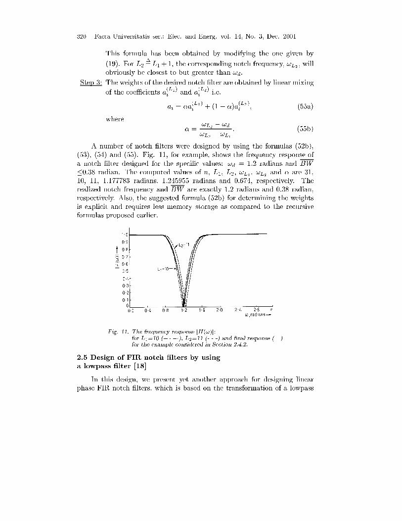
10, 11, 1.177783 radians, 1.245955 radians and 0.674, respectively. Therealized notch frequency and BW are exactly 1.2 radians and 0.38 radian,respectively. Also, the suggested formula (52b) for determining the weightsis explicit and requires less memory storage as compared to the recursiveformulas proposed earlier.
Fig. 11. The frequency response jH(!)j:for L1=10 (� � ��), L2=11 (- - -) and �nal response (|)for the example considered in Section 2.4.2.
2.5 Design of FIR notch �lters by usinga lowpass �lter [18]
In this design, we present yet another approach for designing linearphase FIR notch �lters, which is based on the transformation of a lowpass
S.C. Dutta Roy, B. Kumar, S.B. Jain: FIR notch �lter design ... 321
�lter. This method allows realization of the speci�ed notch frequency (!d)exactly besides resulting in 3-dB rejection bandwidth (BW ) better than thespeci�ed one. The notch �lter may be designed with a maximally at (MF)or equiripple characteristics. We give here the MF design in detail, and thenbrie y mention the equiripple case.
2.5.1 Design
Let HLP (!) be the frequency response of a zero-phase lowpass FIR �ltersuch that
HLP (0) =1;
HLP (!d) =1
2; and
HLP (�) =0:
(56)
We can obtain a notch �lter by using the transformation [37]
H(!) = 2HLP (!)� 1: (57)
Using (56) in (57) results in the notch �lter with
H(0) = 1;
H(�) = �1; and
H(!d) = 0:
(58)
If HLP (!) is maximally at with atness distributed between ! = 0and ! = �, then so is H(!). The design problem of a notch �lter is thusreduced to that of designing a maximally at lowpass �lter HLP (!) suchthat HLP (!) = 1=2 at ! = !d.
A maximally at lowpass �lter HLP (!) can be obtained from Tha-jchayapong et al. [33] which is a modi�cation of Miller's design [20]. Millerhas suggested transforming the zero phase polynomial
H0(z) =nXi=0
Ci(zi + z�i); (59)
into a rational function H(q) (q = � + j) through the bilinear transfor-mation z�1 = (1 � q)=(1 + q). Then by imposing the condition of maximal
atness of H(q), for q = j with m-th degree of atness at = 1 (i.e.

322 Facta Universitatis ser.: Elec. and Energ. vol. 14, No. 3, Dec. 2001
! = �, because = tan(!=2)), the resulting analog �lter has the transferfunction ([33], eqn.2)
H(j) =1
(1 + 2)n
(n�mXk=0
�n
k
�2k
): (60)
Clearly, for a given n, (60) yields n di�erent lowpass �lters as m varies from1 to n. Thajchayapong et al. [33] have suggested a method of obtainingtransitional �lters between two adjacent values of m, say, m1 and m2 =m1 � 1, by modifying (60) as follows
H1(j) =1
(1 + 2)n
(n�m1Xk=0
�n
k
�2k + Cn�m2
2(n�m2)
): (61)
The value of constant Cn�m2in (61) is found by forcing H1(j)j=d =
1=2, where d = tan(!d=2). This gives
Cn�m2=
1
2(n�m2)d
"(1 + 2
d)n
2�
n�m1Xk=0
�n
k
�2kd
#: (62)
Equation (61) is now transformed back to the z-plane by using thetransformation j = (1� z�1)=(1 + z�1), and we �nally obtain [18]
�H1(z) =2�2nzn
(n�m1Xk=0
�n
k
�(�1)k(1� z�1)2k(1 + z�1)2(n�k)
+ Cn�m2(�1)n�m2(1� z�1)2(n�m2)(1 + z�1)2m2
):
(63)
By using the Binomial expansion for (1 + z�1)p, taking causal LPF,H2(z) = z�n �H1(z) and after some manipulations, we �nally get [18]
�H2(z) =2nXi=0
h(i)z�i; n =N � 1
2(64a)
where
h(i) =2�2n
"n�m1Xk=0
2kXq=0
(�1)k+q�n
k
��2k
q
��2n� 2k
i� q
�
+ Cn�m2(�1)n�m2
2m2Xq=0
(�1)i�q�2m2
q
��2n� 2m2
i� q
�# (64b)
S.C. Dutta Roy, B. Kumar, S.B. Jain: FIR notch �lter design ... 323
We may also express h(n� i) given by (64) as
h(n� i) = fA(i) + Cn�m2B(i)g; (65a)
where
A(i) =2�2nn�m1Xk=0
2kXq=0
(�1)k+q�n
k
��2k
q
��2n� 2k
n� i� q
�; (65b)
B(i) =2�2n2m2Xq=0
(�1)q+m2+i
�2m2
q
��2n� 2m2
n� i� q
�: (65c)
ai =
�h(n); i = 0
2h(n� i); i = 1; 2; : : : ; n: (66)
Thus zero phase notch �lter is given by
H(!) =
nXi=0
di cos(i!); (67a)
where
di =
�2a0 � 1; i = 0
2ai; i = 1; 2; : : : ; n
=
�2h(n)� 1; i = 0
4h(n� i); i = 1; 2; : : : ; n:
(67b)
Hence, the coeÆcients di of the desired notch �lter (having notch at! = !d) can be computed from (67) and (65).
The values of n and m, required to compute h(n� i) are obtained fromthe empirical formulas (18) and (19). Readers may refer to a design example,given in [18] ,
Equiripple Design:
The aforementioned design procedure can also be adapted for an equirip-ple notch �lter, ~H(!), by using an equiripple LPF ~HLP (!) in (57). If we
constrain ~HLP (!) as
~HLP (!) =
8>>>>><>>>>>:
2� Æ12
; 0 < j!j < B1
1� Æ22
; j!j = !d
�Æ12; B2 < j!j < �
; (68)
324 Facta Universitatis ser.: Elec. and Energ. vol. 14, No. 3, Dec. 2001
where B2�B1 =BW , and Æ1 and Æ2 are, respectively, the maximum ripplesin the passband and the stopband of the LPF, then the resulting notch �lterwill have
~H(!) =
8><>:
1� Æ1; 0 < j!j < B1
�Æ2; j!j = !d
�1� Æ1; B2 < j!j < �
: (69)
The equiripple linear phase LPF ~HLP (!) may be obtained by any of theconventional methods such as the McClellan and Parks algorithm [27].
Structure:
Equation (57) suggests that an FIR �lter structure meant for lowpassoperation can also be used to perform as a notch �lter without any additionalmultiplication (multiplication by 2 amounts to left shift operation). Thisimplies that if we realize an optimal lowpass �lter by a linear phase FIRstructure, the same can be gainfully exploited as a notch �lter without anyadditional multiplication. The performance of such a notch �lter is alsooptimal.
3. Conclusions
We have given an overview for di�erent design approaches of NotchFilters. In preference to IIR designs, FIR designs are more popular. Severalmethodologies for designing FIR notch �lters have been presented.
We have �rst proposed, in subsection 2.1, an analytic approach for de-signing maximally at, linear phase, notch �lters of the type NF2 ( i.e. with180 degrees of phase shift beyond !d; Fig.2). Recursive formulas have beenderived for computing the coeÆcients of notch �lters in this case. The de-sired notch �lter is obtained by linear combination of two notch �lters withnotch frequency just below and above the speci�ed notch frequency (!d).A `�ne tuning' is necessary to realize the exact notch frequency. Empiricalformulas have been given for �nding the values of N (�lter length), and m(degree of atness of amplitude response at ! = �) to obtain the desiredBW and !d.
As an improvement over the aforementioned approach, a semi-analyticdesign has been proposed in subsection 2.2, which does not require linearcombination of two �lters or even the `�ne tuning'. The computationalrequirement for obtaining the design weights has been simpli�ed in this ap-proach as compared to that in the analytic approach.
S.C. Dutta Roy, B. Kumar, S.B. Jain: FIR notch �lter design ... 325
Another straightforward method for designing the notch �lters has beenproposed in subsection 2.3. Explicit formulas have been derived to deter-mine the weights of maximally at FIR notch �lters by using a second or-der IIR prototype notch �lter. The performance of such a design matchesfavourably with that of the IIR prototype. However, the �lters so designedhave non-linear phase response. These designs may be used in some typicalapplications where linear phase response is not an important consideration.
In yet another approach, in subsection 2.4 , Bernstein Polynomials havebeen used to obtain an explicit formula for designing linear phase maximally at FIR notch �lters. This design methodology leads to much simpler for-mulas for computing the weights as compared to the approaches proposed insubsection 2.1 to subsection 2.3. Another design technique has been evolvedin subsection 2.5 by transforming the given speci�cations (of the notch �l-ter) to an equivalent lowpass �lter. By exploiting the results proposed in [33]and [37], new explicit formula for the design of linear phase maximally atnotch �lters, with exact null at !d, have been obtained. Explicit formulas asderived in these approaches have an edge over the recursive formulas fromthe point of view of computational complexity.
REFERENCES
1. J.W. Adams and A.N. Willson, Jr.: A new approach to FIR digital �lters withfewer multipliers and reduced sensitivity. IEEE Trans. Circuits Sys., Vol. CAS-30,pp. 277-283, May 1983.
2. A. Antoniou: Digital Filters: Analysis and Design. 2nd edn., McGraw-Hill, NewYork, 1986.
3. N.K. Bose: Digital Filters: Theory and Applications. Elsevier Science PublishingCo., Inc., 1985.
4. G.F. Boudreaux and T.W. Parks: Thinning digital �lters: A piecewise exponen-tial approximation approach. IEEE Trans. Acoust. Speech, Signal Process., Vol.ASSP-31, pp. 105-113, February 1983.
5. P.J. Davis: Interpolation and Approximation. Dover, New York, 1975.
6. D.J. DeFatta, J.G. Lucas, W.S. Hodgkiss: Digital Signal Processing: A SystemDesign Approach. John Wiley & Sons Pvt. Ltd., Singapore, 1995.
7. M.H. Er: 3Designing notch �lter with controlled null width. Signal Process., Vol.24, pp. 319-329, September 1991.
8. B. Friedlander and J.O. Smith: Analysis and performance evaluation of anadaptive notch �lter. IEEE Trans. Inform. Theory, Vol. IT-30, pp. 283-295, March1984.
9. C. Fr�oberg: Introduction to Numerical Analysis. Addison-Wesley, Reading, Mas-sachusetts, 1969.
10. R.W. Hamming: Digital Filters. Prentice Hall, Englewood Cli�s, New Jersey, 1977.
11. O. Herrmann: On the approximation problem in nonrecursive digital �lter design.IEEE Trans. Circuit Theory, Vol. CT-18, pp. 411-413, May 1971.
12. K. Hirano, S. Nishimura, and S.K. Mitra: Design of digital notch �lters. IEEETrans. Circuits Sys., Vol. CAS-21, pp. 540-546, July 1974.
326 Facta Universitatis ser.: Elec. and Energ. vol. 14, No. 3, Dec. 2001
13. L.B. Jackson: Digital Filters and Signal Processing. Kluwer Academic Publishers,Hingham, MA, USA, 1989.
14. Shail B. Jain, Balbir Kumar, and S.C. Dutta Roy: Semi-analytic method forthe design of digital FIR �lters with speci�ed notch frequency. Signal Processing,Vol. 59, No.2, pp. 235-241, 1997.
15. Shail B. Jain, Balbir Kumar, and S.C. Dutta Roy: Design of FIR notch�lters by using Bernstein polynomials. International Journal of Circuit Theory andApplications, Vol. 25, No.2, pp. 135-139, March-April, 1997.
16. J.F. Kaiser, and R.W. Hamming: Sharpening the response of a symmetric non-recursive �lter by multiple use of the same �lter. IEEE Trans. Acoust. Speech,Signal Process., ASSP-25, pp. 415-422, October 1977.
17. J.F. Kaiser, and W.A. Reed: Data smoothing using low pass digital �lters. Rev.Sci. Instrum., Vol. 48, pp. 1447-1457, November 1977.
18. B. Kumar, S.B. Jain, and S.C. Dutta Roy: On the design of FIR notch �lters.IETE Journal of Research, Vol. 43, No. 1, pp. 65-68, Jan-Feb 1997.
19. T.I. Laakso, J. Ranta, and S.J. Ovaska: Design and implementation of eÆcientIIR notch �lters with quantization error feedback. IEEE Trans. Instrum. Meas.,Vol. 43, pp. 449-456, June 1994.
20. J.A. Miller: Maximally at nonrecursive digital �lters. Electron. Lett., Vol. 8,pp. 157-158, March 1972.
21. A. Nehorai: A minimal parameter adaptive notch �lter with constrained poles andzeros. IEEE Trans. Acoust. Speech, Signal Process., Vol. ASSP-33, pp. 983-996,August 1985.
22. Y. Neuvo, C.Y. Dong, and S.K. Mitra: Interpolated �nite impulse response�lters. IEEE Trans. Acoust. Speech, Signal Process, Vol. ASSP-32, pp. 563-570,June 1984.
23. A.V. Oppenheim, W.F.G. Mecklenbrauker and R.M. Mersereau: Variablecuto� linear phase digital �lters. IEEE Trans. Circuits Sys., Vol. CAS-23, pp.199-203, April 1976.
24. A.V. Oppenheim and R.W. Schafer: Discrete-Time Signal Processing. PrenticeHall, Englewood Cli�s, New Jersey, 1989.
25. T.W Parks and J.H. McClellan: A program for the design of linear phase �niteimpulse response digital �lters. IEEE Trans. Audio Electroacoust., Vol. AU-20, pp.195-199, August 1972.
26. J.G. Proakis and D.G. Manolakis: Digital Signal Processing Principles, Algo-rithms, and Applications. 3rd Ed., Prentice Hall, Englewood Cli�s, New Jersey,1996.
27. L.R. Rabiner and B. Gold: Theory and Application of Digital Signal Processing.Prentice Hall, Englewood Cli�s, New Jersey, 1975.
28. L.R. Rabiner, J.H. McClellan, and T.W. Parks: FIR digital �lter designtechniques using weighted Chebyshev approximation. Proc. IEEE, Vol. 63, pp.595-610, April 1975.
29. D.V. Bhasker Rao and S.Y. Kung: Adaptive notch �ltering for the retrieval ofsinusoids in noise. IEEE Trans. Acoust., Speech, Signal Process., Vol. ASSP-32,pp. 791-802, August 1984.
30. S.C. Dutta Roy, Shail B. Jain, and B. Kumar: Design of digital FIR notch�lters. IEE Proc.-Vis. Image Signal Process., Vol. 141, No.5, pp. 334-338, October1994.
31. S.C. Dutta Roy, Shail B. Jain, and B. Kumar: Design of digital FIR notch�lters from second order IIR prototype. IETE Journal of Research, Vol. 43, No.4,pp. 275-279, July-Aug 1997.
S.C. Dutta Roy, B. Kumar, S.B. Jain: FIR notch �lter design ... 327
32. D. Slepian: Prolate spheroidal wave functions, Fourier analysis, and uncertainty-V: the discrete case. Bell Systems Tech. J., Vol. 57, pp. 1371-1430, May-June1978.
33. P. Thajchayapong, M. Puangpool, and S. Banjongjit: Maximally at FIR�lter with prescribed cuto� frequency. Electron. Lett., Vol. 16, pp. 514-515, June1980.
34. P.A. Thompson: A constrained recursive adaptive �lter for enhancement of narrow-band signals in white noise. Proc. 12th Asilomar Conf. Circuits, Syst. Comput.,Paci�c Grove, CA, pp. 214-218, November 1978.
35. P.P. Vaidyanathan, and T.Q. Nguyen: Eigen�lters: a new approach to leastsquares FIR �lter design & applications including Nyquist �lters. IEEE Trans.Circuits Sys., Vol. CAS-34, pp. 11-23, January 1987.
36. P.P. Vaidyanathan: Multirate Systems and Filter Banks. Prentice Hall, Engle-wood Cli�s, New Jersey, 1993.
37. T.H. YU, S.K. Mitra, and H. Babic: Design of linear phase notch �lters.S�adh�ana, Vol. 15, pp. 133-155, November 1990.